JP3756364B2 - Game machine - Google Patents
Game machine Download PDFInfo
- Publication number
- JP3756364B2 JP3756364B2 JP33515399A JP33515399A JP3756364B2 JP 3756364 B2 JP3756364 B2 JP 3756364B2 JP 33515399 A JP33515399 A JP 33515399A JP 33515399 A JP33515399 A JP 33515399A JP 3756364 B2 JP3756364 B2 JP 3756364B2
- Authority
- JP
- Japan
- Prior art keywords
- power supply
- ball
- prize ball
- game
- voltage
- Prior art date
- Legal status (The legal status is an assumption and is not a legal conclusion. Google has not performed a legal analysis and makes no representation as to the accuracy of the status listed.)
- Expired - Fee Related
Links
Images


Description
【0001】
【発明の属する技術分野】
本発明は、遊技者の操作に応じて遊技が行われるパチンコ遊技機、コイン遊技機、スロット機等の遊技機に関し、特に、遊技盤における遊技領域において遊技者の操作に応じて遊技が行われる遊技機に関する。
【0002】
【従来の技術】
遊技機として、遊技球などの遊技媒体を発射装置によって遊技領域に発射し、遊技領域に設けられている入賞口などの入賞領域に遊技媒体が入賞すると、所定個の賞球が遊技者に払い出されるものがある。遊技媒体の払い出しは払出機構によって行われる。
【0003】
払出機構は、一般に、賞球制御基板に搭載された賞球制御手段によって制御される。遊技の進行は主基板に搭載された遊技制御手段によって制御されるので、入賞にもとづく賞球個数は、遊技制御手段によって決定され、賞球制御基板に送信される。
【0004】
また、遊技者は、遊技媒体を借り出し、借り出した遊技媒体および入賞に応じて払い出された遊技媒体を用いて遊技を行う。その際、遊技者からの遊技媒体貸し要求はカードユニット等の貸出要求処理装置で一旦受け付けられ、遊技機の貸出制御手段は貸出要求処理装置と通信することによって遊技者からの貸出要求を受け付ける。遊技機は、遊技者からの貸出要求に応じて遊技媒体を貸し出すのであるが、賞球払出を行う払出機構によって玉貸しもなされるように構成されている遊技機も多い。よって、賞球制御手段と貸出制御手段とは一体化された払出制御手段(以下、単に賞球制御手段という。)で構成されていることが多い。また、一般に、賞球制御手段は払出制御マイクロコンピュータを含む構成とされている。
【0005】
【発明が解決しようとする課題】
遊技機に停電等による電源断状態が発生すると、停電等からの復旧時には、最初の状態(例えば、遊技店においてその日最初に遊技機に電源投入されたときの状態)に戻さざるを得ないので、遊技者に不利益がもたらされる可能性がある。例えば、賞球制御手段が貸出要求処理装置を介した貸出要求に対応する全ての遊技媒体の貸出処理を完了していないうちに、停電等による電源断状態が発生すると、電源が復旧したときに、遊技機の状態が初期状態に戻ると貸出遊技媒体の未払出が生じ、遊技者に不利益がもたらされる。
【0006】
そこで、本発明は、遊技機に停電等による電源断状態が発生しても、遊技媒体に貸出に関して遊技者に不利益を与えることのない遊技機を提供することを目的とする。
【0007】
【課題を解決するための手段】
本発明による遊技機は、遊技者が所定の遊技を行うことが可能な遊技機であって、遊技に用いられる遊技媒体を貸し出すことが可能な払出装置と、遊技媒体貸出要求に応じて払出装置から遊技媒体を払い出す遊技媒体貸出制御を行う払出制御マイクロコンピュータと、遊技機に設けられ払出装置から払い出された遊技媒体を検出する貸し遊技媒体検出手段と、貸し遊技媒体検出手段に供給される電圧よりも高い直流電圧の電源の状態を監視して、該電源の電圧が貸し遊技媒体検出手段に供給される電圧よりも高い電圧である所定電圧に低下したときに所定の検出信号を出力する電源監視手段と、電源監視手段が監視する直流電圧と同一の直流電圧を監視し、該直流電圧が、電源監視手段が所定の検出信号を出力するときの所定電圧よりも低く設定された検出電圧になったときに払出制御マイクロコンピュータの動作を禁止させるためのリセット信号を出力するリセット信号出力手段と、遊技媒体貸出要求にもとづいた遊技媒体の払出数のうち払い出しが完了していない未払出数を特定可能な情報を、遊技機への電力供給が停止されたときであっても少なくとも所定期間において保持可能な記憶手段とを備え、払出制御マイクロコンピュータは、貸し遊技媒体検出手段から検出出力が出力されたときに未払出数を減算する処理を実行する減算手段と、電源監視手段からの所定の検出信号に応じて、払出装置の動作を停止させるとともに、電力供給が停止したことを示す電力供給停止情報を記憶手段に格納する電力供給停止時処理を実行する電力供給停止時処理実行手段と、電力供給が開始されたときに、記憶手段に電力供給停止情報が保存されていたことを条件に、記憶手段に記憶されている未払出数を特定可能な情報にもとづいて遊技媒体の払出制御を再開させる復旧手段とを含み、リセット信号出力手段は、電源監視手段が所定の検出信号を出力するときから少なくとも電力供給停止時処理完了後に成立するように設定された検出条件が成立したときにリセット信号を出力し、払出制御マイクロコンピュータは、リセット信号出力手段からのリセット信号の入力に応じて動作禁止状態とされることを特徴とする。
【0010】
電力供給停止時処理実行手段は、電力供給停止時処理で、記憶手段へのアクセスを防止する処理を行うように構成されていてもよい。
【0011】
電力供給停止時処理実行手段は、電力供給停止時処理で、記憶手段の記憶内容に関連した演算の結果得られるチェックデータを記憶手段に保存する処理を行うように構成されていてもよい。
また、払出制御マイクロコンピュータは、電力供給開始時にチェックデータにもとづくチェックを行い、チェック結果が正常でなければ記憶手段に保存されている遊技媒体の未払出数に関する情報を無効化するように構成されていてもよい。
【0012】
電源監視手段からの検出信号は払出制御マイクロコンピュータの割込端子に入力され、払出制御マイクロコンピュータは、割込端子への入力にもとづいて電力供給停止時処理を実行するように構成されていてもよい。
【0013】
未払出数を特定可能な情報を少なくとも所定期間において保持可能な記憶手段は、払出制御マイクロコンピュータに内蔵される構成であってもよい。すなわち、記憶手段は、例えば、マイクロコンピュータに内蔵されているメモリ(RAM)であってもよい。
【0017】
【発明の実施の形態】
以下、本発明の一実施形態を図面を参照して説明する。
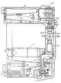
まず、遊技機の一例であるパチンコ遊技機の全体の構成について説明する。図1はパチンコ遊技機1を正面からみた正面図、図2はパチンコ遊技機1の内部構造を示す全体背面図、図3はパチンコ遊技機1の遊技盤を背面からみた背面図である。なお、ここでは、遊技機の一例としてパチンコ遊技機を示すが、本発明はパチンコ遊技機に限られず、例えばコイン遊技機等であってもよい。また、画像式の遊技機やスロット機に適用することもできる。
【0018】
図1に示すように、パチンコ遊技機1は、額縁状に形成されたガラス扉枠2を有する。ガラス扉枠2の下部表面には打球供給皿3がある。打球供給皿3の下部には、打球供給皿3からあふれた景品玉を貯留する余剰玉受皿4と打球を発射する打球操作ハンドル(操作ノブ)5が設けられている。ガラス扉枠2の後方には、遊技盤6が着脱可能に取り付けられている。また、遊技盤6の前面には遊技領域7が設けられている。
【0019】
遊技領域7の中央付近には、複数種類の図柄を可変表示するための可変表示部9と7セグメントLEDによる可変表示器10とを含む可変表示装置8が設けられている。この実施の形態では、可変表示部9には、「左」、「中」、「右」の3つの図柄表示エリアがある。可変表示装置8の側部には、打球を導く通過ゲート11が設けられている。通過ゲート11を通過した打球は、玉出口13を経て始動入賞口14の方に導かれる。通過ゲート11と玉出口13との間の通路には、通過ゲート11を通過した打球を検出するゲートスイッチ12がある。また、始動入賞口14に入った入賞球は、遊技盤6の背面に導かれ、始動口スイッチ17によって検出される。また、始動入賞口14の下部には開閉動作を行う可変入賞球装置15が設けられている。可変入賞球装置15は、ソレノイド16によって開状態とされる。
【0020】
可変入賞球装置15の下部には、特定遊技状態(大当り状態)においてソレノイド21によって開状態とされる開閉板20が設けられている。この実施の形態では、開閉板20が大入賞口を開閉する手段となる。開閉板20から遊技盤6の背面に導かれた入賞球のうち一方(Vゾーン)に入った入賞球はVカウントスイッチ22で検出される。また、開閉板20からの入賞球はカウントスイッチ23で検出される。可変表示装置8の下部には、始動入賞口14に入った入賞球数を表示する4個の表示部を有する始動入賞記憶表示器18が設けられている。この例では、4個を上限として、始動入賞がある毎に、始動入賞記憶表示器18は点灯している表示部を1つずつ増やす。そして、可変表示部9の可変表示が開始される毎に、点灯している表示部を1つ減らす。
【0021】
遊技盤6には、複数の入賞口19,24が設けられ、遊技球の入賞口19,24への入賞は入賞口スイッチ19a,24aによって検出される。遊技領域7の左右周辺には、遊技中に点滅表示される装飾ランプ25が設けられ、下部には、入賞しなかった打球を吸収するアウト口26がある。また、遊技領域7の外側の左右上部には、効果音を発する2つのスピーカ27が設けられている。遊技領域7の外周には、遊技効果LED28aおよび遊技効果ランプ28b,28cが設けられている。
【0022】
そして、この例では、一方のスピーカ27の近傍に、景品玉払出時に点灯する賞球ランプ51が設けられ、他方のスピーカ27の近傍に、補給玉が切れたときに点灯する球切れランプ52が設けられている。さらに、図1には、パチンコ遊技台1に隣接して設置され、プリペイドカードが挿入されることによって玉貸しを可能にするカードユニット50も示されている。
【0023】
カードユニット50には、使用可能状態であるか否かを示す使用可表示ランプ151、カード内に記録された残額情報に端数(100円未満の数)が存在する場合にその端数を打球供給皿3の近傍に設けられる度数表示LEDに表示させるための端数表示スイッチ152、カードユニット50がいずれの側のパチンコ遊技機1に対応しているのかを示す連結台方向表示器153、カードユニット50内にカードが投入されていることを示すカード投入表示ランプ154、記録媒体としてのカードが挿入されるカード挿入口155、およびカード挿入口155の裏面に設けられているカードリーダライタの機構を点検する場合にカードユニット50を解放するためのカードユニット錠156が設けられている。
【0024】
打球発射装置から発射された打球は、打球レールを通って遊技領域7に入り、その後、遊技領域7を下りてくる。打球が通過ゲート11を通ってゲートスイッチ12で検出されると、可変表示器10の表示数字が連続的に変化する状態になる。また、打球が始動入賞口14に入り始動口スイッチ17で検出されると、図柄の変動を開始できる状態であれば、可変表示部9内の図柄が回転を始める。図柄の変動を開始できる状態でなければ、始動入賞記憶を1増やす。
【0025】
可変表示部9内の画像の回転は、一定時間が経過したときに停止する。停止時の画像の組み合わせが大当り図柄の組み合わせであると、大当り遊技状態に移行する。すなわち、開閉板20が、一定時間経過するまで、または、所定個数(例えば10個)の打球が入賞するまで開放する。そして、開閉板20の開放中に打球が特定入賞領域に入賞しVカウントスイッチ22で検出されると、継続権が発生し開閉板20の開放が再度行われる。継続権の発生は、所定回数(例えば15ラウンド)許容される。
【0026】
停止時の可変表示部9内の画像の組み合わせが確率変動を伴う大当り図柄の組み合わせである場合には、次に大当りとなる確率が高くなる。すなわち、高確率状態という遊技者にとってさらに有利な状態となる。また、可変表示器10における停止図柄が所定の図柄(当り図柄)である場合に、可変入賞球装置15が所定時間だけ開状態になる。さらに、高確率状態では、可変表示器10における停止図柄が当り図柄になる確率が高められるとともに、可変入賞球装置15の開放時間と開放回数が高められる。
【0027】
次に、パチンコ遊技機1の裏面の構造について図2を参照して説明する。
可変表示装置8の背面では、図2に示すように、機構板36の上部に景品玉タンク38が設けられ、パチンコ遊技機1が遊技機設置島に設置された状態でその上方から景品玉が景品玉タンク38に供給される。景品玉タンク38内の景品玉は、誘導樋39を通って玉払出装置に至る。
【0028】
機構板36には、中継基板30を介して可変表示部9を制御する可変表示制御ユニット29、基板ケース32に覆われ遊技制御用マイクロコンピュータ等が搭載された遊技制御基板(主基板)31、可変表示制御ユニット29と遊技制御基板31との間の信号を中継するための中継基板33、および景品玉の払出制御を行う賞球制御用マイクロコンピュータ等が搭載された賞球制御基板(払出制御基板)37が設置されている。さらに、機構板36の下部には、モータの回転力を利用して打球を遊技領域7に発射する打球発射装置34と、遊技効果ランプ・LED28a,28b,28c、賞球ランプ51および球切れランプ52に信号を送るためのランプ制御基板35が設置されている。
【0029】
また、図3はパチンコ遊技機1の遊技盤を背面からみた背面図である。誘導樋39を通った玉は、図3に示されるように、球切れ検出器187a,187bを通過して玉供給樋186a,186bを経て玉払出装置97に至る。玉払出装置97から払い出された景品玉は、連絡口45を通ってパチンコ遊技機1の前面に設けられている打球供給皿3に供給される。連絡口45の側方には、パチンコ遊技機1の前面に設けられている余剰玉受皿4に連通する余剰玉通路46が形成されている。入賞にもとづく景品玉が多数払い出されて打球供給皿3が満杯になり、ついには景品玉が連絡口45に到達した後さらに景品玉が払い出されると景品玉は、余剰玉通路46を経て余剰玉受皿4に導かれる。さらに景品玉が払い出されると、感知レバー47が満タンスイッチ48を押圧して満タンスイッチ48がオンする。その状態では、玉払出装置97内のステッピングモータの回転が停止して玉払出装置97の動作が停止するとともに、必要に応じて打球発射装置34の駆動も停止する。
【0030】
賞球払出制御を行うために、入賞口スイッチ(図示せず)、始動口スイッチ17およびVカウントスイッチ22からの信号が、主基板31に送られる。主基板31のCPU56は、始動口スイッチ17がオンすると6個の賞球払出に対応した入賞が発生したことを知る。また、カウントスイッチ23がオンすると15個の賞球払出に対応した入賞が発生したことを知る。そして、入賞口スイッチがオンすると10個の賞球払出に対応した入賞が発生したことを知る。なお、この実施の形態では、例えば、入賞口24に入賞した遊技球は、入賞口24からの入賞球流路に設けられている入賞口スイッチ24aで検出され、入賞口19に入賞した遊技球は、入賞口19からの入賞球流路に設けられている入賞口スイッチ19aで検出される。
【0031】
次に、機構板36に設置されている中間ベースユニットの構成について説明する。中間ベースユニットには、玉供給樋186a,186bや玉払出装置97が設置される。図4に示すように、中間ベースユニットの上下には連結凹突部182が形成されている。連結凹突部182は、中間ベースユニットと機構板36の上部ベースユニットおよび下部ベースユニットを連結固定するものである。
【0032】
中間ベースユニットの上部には通路体184が固定されている。そして、通路体184の下部に玉払出装置97が固定されている。通路体184は、カーブ樋174(図3参照)によって流下方向を左右方向に変換された2列の景品玉を流下させる景品玉通路186a,186bを有する。景品玉通路186a,186bの上流側には、球切れスイッチ187a,187bが設置されている。球切れスイッチ187a,187bは、景品玉通路186a,186b内の景品玉の有無を検出するものであって、球切れスイッチ187a,187bが景品玉を検出しなくなると玉払出装置97における払出モータ(図4において図示せず)の回転を停止して球払出が不動化される。
【0033】
なお、球切れスイッチ187a,187bは、景品玉通路186a,186bに27〜28個の景品玉が存在することを検出できるような位置に係止片188によって係止されている。
【0034】
通路体184の中央部は、内部を流下する景品玉の玉圧を弱めるように、左右に湾曲する形状に形成されている。そして、景品玉通路186a,186bの間に止め穴189が形成されている。止め穴189の裏面は中間ベースユニットに設けられている取付ボスがはめ込まれる。その状態で止めねじがねじ止めされて、通路体184は中間ベースユニットに固定される。なお、ねじ止めされる前に、中間ベースユニットに設けられている係止突片185によって通路体184の位置合わせを行えるようになっている。
【0035】
通路体184の下方には、玉払出装置97に景品玉を供給するとともに故障時等には玉払出装置97への景品玉の供給を停止する玉止め装置190が設けられている。玉止め装置190の下方に設置される玉払出装置97は、直方体状のケース198の内部に収納されている。ケース198の左右4箇所には突部が設けられている。各突部が中間ベースユニットに設けられている位置決め突片に係った状態で、中間ベースユニットの下部に設けられている弾性係合片にケース198の下端がはめ込まれる。
【0036】
図5は玉払出装置97の分解斜視図である。玉払出装置97の構成および作用を図5を参照して説明する。この実施形態における玉払出装置97は、ステッピングモータ(払出モータ)289がスクリュー288を回転させることによりパチンコ玉を1個ずつ払い出す。なお、玉払出装置97は、入賞にもとづく景品玉だけでなく、貸し出すべき遊技玉も払い出す。
【0037】
図5に示すように、玉払出装置97は、2つのケース198a,198bを有する。それぞれのケース198a,198bの左右2箇所に、玉払出装置97の設置位置上部に設けられた位置決め突片に当接される係合突部280が設けられている。また、それぞれのケース198a,198bには、玉供給路281a,281bが形成されている。玉供給路281a,281bは湾曲面282a,282bを有し、湾曲面282a,282bの終端の下方には、玉送り水平路284a,284bが形成されている。さらに、玉送り水平路284a,284bの終端に玉排出路283a,283bが形成されている。
【0038】
玉供給路281a,281b、玉送り水平路284a,284b、玉排出路283a,283bは、ケース198a,198bをそれぞれ前後に区画する区画壁295a,295bの前方に形成されている。また、区画壁295a,295bの前方において、玉圧緩衝部材285がケース198a,198b間に挟み込まれる。玉圧緩衝部材285は、玉払出装置97に供給される玉を左右側方に振り分けて玉供給路281a,281bに誘導する。
【0039】
また、玉圧緩衝部材285の下部には、発光素子(LED)286と受光素子(図示せず)とによる払出モータ位置センサが設けられている。発光素子286と受光素子とは、所定の間隔をあけて設けられている。そして、この間隔内に、スクリュー288の先端が挿入されるようになっている。なお、玉圧緩衝部材285は、ケース198a,198bが張り合わされたときに、完全にその内部に収納固定される。
【0040】
玉送り水平路284a,284bには、払出モータ289によって回転させられるスクリュー288が配置されている。払出モータ289はモータ固定板290に固定され、モータ固定板290は、区画壁295a,295bの後方に形成される固定溝291a,291bにはめ込まれる。その状態で払出モータ289のモータ軸が区画壁295a,295bの前方に突出するので、その突出の前方にスクリュー288が固定される。スクリュー288の外周には、払出モータ289の回転によって玉送り水平路284a,284bに載置された玉を前方に移動させるための螺旋突起288aが設けられている。
【0041】
そして、スクリュー288の先端には、発光素子286を収納するように凹部が形成され、その凹部の外周には、2つの切欠部292が互いに180度離れて形成されている。従って、スクリュー288が1回転する間に、発光素子286からの光は、切欠部292を介して受光素子で2回検出される。
【0042】
つまり、発光素子286と受光素子とによる払出モータ位置センサは、スクリュー288を定位置で停止するためのものであり、かつ、払出動作が行われた旨を検出するものである。なお、発光素子286、受光素子および払出モータ289からの配線は、まとめられてケース198a,198bの後部下方に形成された引出穴から外部に引き出されコネクタに結線される。
【0043】
玉が玉送り水平路284a,284bに載置された状態において、払出モータ289が回転すると、スクリュー288の螺旋突起288aによって、玉は、玉送り水平路284a,284b上を前方に向かって移動する。そして、遂には、玉送り水平路284a,284bの終端から玉排出路283a,283bに落下する。このとき、左右の玉送り水平路284a,284bからの落下は交互に行われる。すなわち、スクリュー288が半回転する毎に一方から1個の玉が落下する。従って、1個の玉が落下する毎に、発光素子286からの光が受光素子によって検出される。
【0044】
図4に示すように、玉払出装置97の下方には、球振分部材311が設けられている。球振分部材311は、振分用ソレノイド310によって駆動される。例えば、ソレノイド310のオン時には、球振分部材311は右側に倒れ、オフ時には左側に倒れる。振分用ソレノイド310の下方には、近接スイッチによる賞球カウントスイッチ301Aおよび玉貸しカウントスイッチ301Bが設けられている。入賞にもとづく賞球時には、球振分部材311は右側に倒れ、玉排出路283a,283bからの玉はともに賞球カウントスイッチ301Aを通過する。また、玉貸し時には、球振分部材311は左側に倒れ、玉排出路283a,283bからの玉はともに玉貸しカウントスイッチ301Bを通過する。
【0045】
このように、球振分部材311を設けることによって、2条の玉流路を落下してきた玉は、賞球カウントスイッチ301Aと玉貸しカウントスイッチ301Bとのうちのいずれか一方しか通過しない。従って、賞球であるのか玉貸しであるのかの判断をすることなく、賞球カウントスイッチ301Aと玉貸しカウントスイッチ301Bの検出出力から、直ちに賞球数または玉貸し数を把握することができる。
【0046】
図6は、主基板31における回路構成の一例を示すブロック図である。なお、図6には、賞球制御基板37、ランプ制御基板35、音制御基板70、発射制御基板91および表示制御基板80も示されている。主基板31には、プログラムに従ってパチンコ遊技機1を制御する基本回路53と、ゲートスイッチ12、始動口スイッチ17、Vカウントスイッチ22、カウントスイッチ23および入賞口スイッチ19a,24aからの信号を基本回路53に与えるスイッチ回路58と、可変入賞球装置15を開閉するソレノイド16および開閉板20を開閉するソレノイド21を基本回路53からの指令に従って駆動するソレノイド回路59と、始動記憶表示器18の点灯および滅灯を行うとともに7セグメントLEDによる可変表示器10と装飾ランプ25とを駆動するランプ・LED回路60とが搭載されている。
【0047】
また、基本回路53から与えられるデータに従って、大当りの発生を示す大当り情報、可変表示部9の画像表示開始に利用された始動入賞球の個数を示す有効始動情報、確率変動が生じたことを示す確変情報等をホール管理コンピュータ等のホストコンピュータに対して出力する情報出力回路64を含む。
【0048】
基本回路53は、ゲーム制御用のプログラム等を記憶するROM54、ワークメモリとして使用される記憶手段の一例であるRAM55、制御用のプログラムに従って制御動作を行うCPU56およびI/Oポート部57を含む。この実施の形態では、ROM54,RAM55はCPU56に内蔵されている。すなわち、CPU56は、1チップマイクロコンピュータである。なお、1チップマイクロコンピュータは、少なくともRAM55が内蔵されていればよく、ROM54およびI/Oポート部57は外付けであっても内蔵されていてもよい。また、I/Oポート部57は、マイクロコンピュータにおける情報入出力可能な端子である。
【0049】
さらに、主基板31には、電源投入時に基本回路53をリセットするための初期リセット回路65と、基本回路53から与えられるアドレス信号をデコードしてI/Oポート部57のうちのいずれかのI/Oポートを選択するための信号を出力するアドレスデコード回路67とが設けられている。
なお、玉払出装置97から主基板31に入力されるスイッチ情報もあるが、図6ではそれらは省略されている。
【0050】
遊技球を打撃して発射する打球発射装置は発射制御基板91上の回路によって制御される駆動モータ94で駆動される。そして、駆動モータ94の駆動力は、操作ノブ5の操作量に従って調整される。すなわち、発射制御基板91上の回路によって、操作ノブ5の操作量に応じた速度で打球が発射されるように制御される。
【0051】
図7は、電源監視および電源バックアップのためのCPU56周りの一構成例を示すブロック図である。図7に示すように、電源基板に搭載されている第1の電源監視回路(第1の電源監視手段)からの電圧低下信号が、CPU56のマスク不能割込端子(NMI端子)に接続されている。第1の電源監視回路は、遊技機が使用する各種直流電源のうちのいずれかの電源の電圧を監視して電源電圧低下を検出する回路である。従って、CPU56は、割込処理によって電源断の発生を確認することができる。
【0052】
主基板31において、第1の電源監視手段からの電圧低下信号は、入力バッファ回路900を介してCPU56側に入力されている。ここでは、入力バッファ回路900として74HC244を例示するが、入力バッファ機能を有する回路であるならばどのような回路を用いてもよい。また、入力バッファ回路900は、電源基板側から主基板31の内部側への方向にのみ信号を通過させる不可逆性素子である。
【0053】
主基板31には、第2の電源監視回路903が搭載されている。この例では、第2の電源監視回路903において、電源監視用IC904が、第1の電源監視回路が監視する電源電圧と等しい電源電圧である+30V電源電圧を監視して電圧値が所定値以下になるとローレベルの電圧低下信号を発生する。そして、例えば、電源基板に搭載される第1の電源監視回路の検出電圧(電圧低下信号を出力することになる電圧)を+21Vとし、第2の電源監視回路903の検出電圧を+9Vとする。
【0054】
よって、この例では、第1の電源監視手段が検出信号を出力することになる第1検出条件は+30V電源電圧が+21Vにまで低下したことであり、第2の電源監視手段が検出信号を出力することになる第2検出条件は+30V電源電圧が+9Vにまで低下したことになる。ただし、ここで用いられている電圧値は一例であって、他の値を用いてもよい。
【0055】
そのように構成した場合には、同一の電圧を監視するので、第1の電圧監視回路が電圧低下信号を出力するタイミングと第2の電圧監視回路が電圧低下信号を出力するタイミングの差を所望の所定期間に確実に設定することができる。所望の所定期間とは、第1の電源監視回路からの電圧低下信号に応じて電力供給停止時処理を開始してから電力供給停止時処理が確実に完了するまでの期間である。
【0056】
第2の電源監視回路903からの電圧低下信号は、初期リセット回路65からの初期リセット信号と論理和をとられた後に、CPU56のリセット端子に入力される。従って、CPU56は、初期リセット回路65からの初期リセット信号がローレベルを呈しているとき、または、第2の電源監視回路903からの電圧低下信号がローレベルを呈しているときに、リセット状態(非動作状態)になる。
【0057】
なお、初期リセット回路65のリセットIC651は、遊技機に電源が投入され+5V電源の電圧が上昇していくときに、+5V電源電圧が所定値以上になると、出力信号をハイレベルにする。すなわち、初期リセット信号をオフ状態にする。
【0058】
CPU56等の駆動電源である+5V電源から電力が供給されていない間、RAMの少なくとも一部は、電源基板から供給されるバックアップ電源によってバックアップされ、遊技機に対する電源が断しても内容は保存される。そして、+5V電源が復旧すると、初期リセット回路65からリセット信号が発せられるので、CPU56は、通常の動作状態に復帰する。そのとき、必要なデータがバックアップされているので、停電等からの復旧時には停電発生時の遊技状態に復帰することができる。
【0059】
図8は、遊技機の電源基板910の一構成例を示すブロック図である。電源基板910は、主基板31、表示制御基板80、音制御基板70、ランプ制御基板35および賞球制御基板37等の電気部品制御基板と独立して設置され、遊技機内の各電気部品制御基板および機構部品が使用する電圧を生成する。この例では、AC24V、DC+30V、DC+21V、DC+12VおよびDC+5Vを生成する。また、バックアップ電源となるコンデンサ916は、DC+5Vすなわち各基板上のIC等を駆動する電源のラインから充電される。
【0060】
トランス911は、交流電源からの交流電圧を24Vに変換する。AC24V電圧は、コネクタ915に出力される。また、整流回路912は、AC24Vから+30Vの直流電圧を生成し、DC−DCコンバータ913およびコネクタ915に出力する。DC−DCコンバータ913は、+21V、+12Vおよび+5Vを生成してコネクタ915に出力する。コネクタ915は例えば中継基板に接続され、中継基板から各電気部品制御基板および機構部品に必要な電圧の電力が供給される。なお、トランス911の入力側には、遊技機に対する電源供給を停止したり開始させたりするための電源スイッチ918が設置されている。
【0061】
DC−DCコンバータ913からの+5Vラインは分岐してバックアップ+5Vラインを形成する。バックアップ+5Vラインとグラウンドレベルとの間には大容量のコンデンサ916が接続されている。コンデンサ916は、遊技機に対する電力供給が遮断されたときの電気部品制御基板のバックアップRAM(電源バックアップされているRAMすなわち記憶内容保持状態となりうる記憶手段)に対して記憶状態を保持できるように電力を供給するバックアップ電源となる。また、+5Vラインとバックアップ+5Vラインとの間に、逆流防止用のダイオード917が挿入される。
【0062】
なお、バックアップ電源として、+5V電源から充電可能な電池を用いてもよい。電池を用いる場合には、+5V電源から電力供給されない状態が所定時間継続すると容量がなくなるような充電池が用いられる。
【0063】
また、電源基板910には、上述した第1の電源回路を構成する電源監視用IC902が搭載されている。電源監視用IC902は、+30V電源電圧を導入し、+30V電源電圧を監視することによって電源断の発生を検出する。具体的には、+30V電源電圧が所定値(この例では+21V)以下になったら、電源断が生ずるとして電圧低下信号を出力する。なお、監視対象の電源電圧は、各電気部品制御基板に搭載されている回路素子の電源電圧(この例では+5V)よりも高い電圧であることが好ましい。この例では、交流から直流に変換された直後の電圧である+30Vが用いられている。電源監視用IC902からの電圧低下信号は、主基板31や賞球制御基板37等に供給される。
【0064】
電源監視用IC902が電源断を検知するための所定値は、通常時の電圧より低いが、各電気部品制御基板上のCPUが暫くの間動作しうる程度の電圧である。また、電源監視用IC902が、CPU等の回路素子を駆動するための電圧(この例では+5V)よりも高く、また、交流から直流に変換された直後の電圧を監視するように構成されているので、CPUが必要とする電圧に対して監視範囲を広げることができる。従って、より精密な監視を行うことができる。さらに、監視電圧として+30Vを用いる場合には、遊技機の各種スイッチに供給される電圧が+12Vであることから、電源瞬断時のスイッチオン誤検出の防止も期待できる。すなわち、+30V電源の電圧を監視すると、+30V作成の以降に作られる+12Vが落ち始める以前の段階でそれの低下を検出できる。よって、+12V電源の電圧が低下するとスイッチ出力がオン状態を呈するようになるが、+12Vより早く低下する+30V電源電圧を監視して電源断を認識すれば、スイッチ出力がオン状態を呈する前に電源復旧待ちの状態に入ってスイッチ出力を検出しない状態となることができる。
【0065】
また、電源監視用IC902は、電気部品制御基板とは別個の電源基板910に搭載されているので、第1の電源監視回路から複数の電気部品制御基板に電圧低下信号を供給することができる。電圧低下信号を必要とする電気部品制御基板が幾つあっても第1の電源監視手段は1つ設けられていればよいので、各電気部品制御基板における各電気部品制御手段が後述する電源復帰制御を行っても、遊技機のコストはさほど上昇しない。
【0066】
なお、図8に示された構成では、電源監視用IC902の検出出力(電圧低下信号)は、バッファ回路918,919を介してそれぞれの電気部品制御基板(この例では、主基板31と賞球制御基板37)に伝達されるが、例えば、1つの検出出力を中継基板に伝達し、中継基板から各電気部品制御基板に同じ信号を分配する構成でもよい。
【0067】
次に遊技機の動作について説明する。
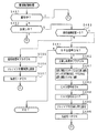
図9は、主基板31におけるCPU56が実行するメイン処理を示すフローチャートである。遊技機に対する電源が投入されると、メイン処理において、CPU56は、まず、停電からの復旧時であったか否か確認する(ステップS1)。停電からの復旧時であったか否かは、例えば、電源断時にバックアップRAM領域に設定される電源断フラグによって確認される。
【0068】
停電からの復旧時であった場合には、バックアップRAM領域のデータチェック(この例ではパリティチェック)を行う(ステップS3)。不測の電源断が生じた後に復旧した場合には、バックアップRAM領域のデータは保存されていたはずであるから、チェック結果は正常になる。チェック結果が正常でない場合には、内部状態を電源断時の状態に戻すことができないので、停電復旧時でない電源投入時に実行される初期化処理を実行する(ステップS4,S2)。
【0069】
チェック結果が正常であれば、CPU56は、内部状態を電源断時の状態に戻すための遊技状態復旧処理を行うとともに(ステップS5)、電源断フラグをクリアする(ステップS6)。
【0070】
停電からの復旧時でない場合には、CPU56は、通常の初期化処理を実行する(ステップS1,S2)。その後、メイン処理では、タイマ割込フラグの監視(ステップS6)の確認が行われるループ処理に移行する。なお、ループ内では、表示用乱数更新処理(ステップS7)も実行される。
【0071】
なお、ここでは、ステップS1で停電からの復旧か否かを確認し、停電からの復旧時であればパリティチェックを行ったが、最初に、パリティチェックを実行し、チェック結果が正常でなければ停電からの復旧ではないと判断してステップS2の初期化処理を実行し、チェック結果が正常であれば遊技状態復帰処理を行ってもよい。すなわち、パリティチェックの結果をもって停電からの復旧であるか否かを判断してもよい。
【0072】
また、停電復旧処理を実行するか否か判断する場合に、すなわち、遊技状態を復旧するか否か判断する際に、保存されていたRAMデータにおける特別プロセスフラグ等や始動入賞記憶数データによって、遊技機が遊技待機状態(特別図柄変動中でなく、大当り遊技中でなく、確変中でなく、また、始動入賞記憶がない状態)であることが確認されたら、遊技状態復旧処理を行わずに初期化処理を実行するようにしてもよい。
【0073】
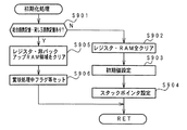
通常の初期化処理では、図10に示すように、レジスタおよびRAMのクリア処理(ステップS2a)と、必要な初期値設定処理(ステップS2b)が行われた後に、2ms毎に定期的にタイマ割込がかかるようにCPU56に設けられているタイマレジスタの初期設定(タイムアウトが2msであることと繰り返しタイマが動作する設定)が行われる(ステップS2c)。すなわち、ステップS2cで、タイマ割込を能動化する処理と、タイマ割込インタバルを設定する処理とが実行される。
【0074】
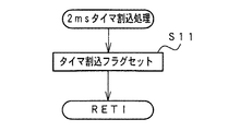
従って、この実施の形態では、CPU56の内部タイマが繰り返しタイマ割込を発生するように設定される。この実施の形態では、繰り返し周期は2msに設定される。そして、図11に示すように、タイマ割込が発生すると、CPU56は、タイマ割込フラグをセットする(ステップS11)。
【0075】
CPU56は、ステップS8において、タイマ割込フラグがセットされたことを検出すると、タイマ割込フラグをリセットするとともに(ステップS9)、遊技制御処理を実行する(ステップS10)。以上の制御によって、この実施の形態では、遊技制御処理は2ms毎に起動されることになる。なお、この実施の形態では、タイマ割込処理ではフラグセットのみがなされ、遊技制御処理はメイン処理において実行されるが、タイマ割込処理で遊技制御処理を実行してもよい。
【0076】
図12は、ステップS10の遊技制御処理を示すフローチャートである。遊技制御処理において、CPU56は、まず、表示制御基板80に送出される表示制御コマンドをRAM55の所定の領域に設定する処理を行った後に(表示制御データ設定処理:ステップS21)、表示制御コマンドを出力する処理を行う(表示制御データ出力処理:ステップS22)。
【0077】
次いで、各種出力データの格納領域の内容を各出力ポートに出力する処理を行う(データ出力処理:ステップS23)。また、ホール管理用コンピュータに出力される大当り情報、始動情報、確率変動情報などの出力データを格納領域に設定する出力データ設定処理を行う(ステップS24)。さらに、パチンコ遊技機1の内部に備えられている自己診断機能によって種々の異常診断処理が行われ、その結果に応じて必要ならば警報が発せられる(エラー処理:ステップS25)。
【0078】
次に、遊技制御に用いられる大当り判定用の乱数等の各判定用乱数を示す各カウンタを更新する処理を行う(ステップS26)。
【0079】
さらに、CPU56は、特別図柄プロセス処理を行う(ステップS27)。特別図柄プロセス制御では、遊技状態に応じてパチンコ遊技機1を所定の順序で制御するための特別図柄プロセスフラグに従って該当する処理が選び出されて実行される。そして、特別図柄プロセスフラグの値は、遊技状態に応じて各処理中に更新される。また、普通図柄プロセス処理を行う(ステップS28)。普通図柄プロセス処理では、7セグメントLEDによる可変表示器10を所定の順序で制御するための普通図柄プロセスフラグに従って該当する処理が選び出されて実行される。そして、普通図柄プロセスフラグの値は、遊技状態に応じて各処理中に更新される。
【0080】
さらに、CPU56は、スイッチ回路58を介して、ゲートセンサ12、始動口センサ17、カウントセンサ23および入賞口スイッチ19a,24aの状態を入力し、各入賞口や入賞装置に対する入賞があったか否か判定する(スイッチ処理:ステップS29)。CPU56は、さらに、停止図柄の種類を決定する乱数等の表示用乱数を更新する処理を行う(ステップS30)。
【0081】
また、CPU56は、賞球制御基板37との間の信号処理を行う(ステップS31)。すなわち、所定の条件が成立すると賞球制御基板37に賞球制御コマンドを出力する。賞球制御基板37に搭載されている賞球制御用CPUは、賞球制御コマンドに応じて玉払出装置97を駆動する。
【0082】
以上のように、メイン処理には遊技制御処理に移行すべきか否かを判定する処理が含まれ、CPU56の内部タイマが定期的に発生するタイマ割込にもとづくタイマ割込処理で遊技制御処理に移行すべきか否かを判定するためのフラグがセットされるので、遊技制御処理の全てが確実に実行される。つまり、遊技制御処理の全てが実行されるまでは、次回の遊技制御処理に移行すべきか否かの判定が行われないので、遊技制御処理中の全ての各処理が実行完了することは保証されている。
【0083】
従来の一般的な遊技制御処理は、定期的に発生する外部割込によって、強制的に最初の状態に戻されていた。図12に示された例に則して説明すると、例えば、ステップS31の処理中であっても、強制的にステップS21の処理に戻されていた。つまり、遊技制御処理中の全ての各処理が実行完了する前に、次回の遊技制御処理が開始されてしまう可能性があった。
【0084】
なお、ここでは、主基板31のCPU56が実行する遊技制御処理は、CPU56の内部タイマが定期的に発生するタイマ割込にもとづくタイマ割込処理でセットされるフラグに応じて実行されたが、定期的に(例えば2ms毎)信号を発生するハードウェア回路を設け、その回路からの信号をCPU56の外部割込端子に導入し、割込信号によって遊技制御処理に移行すべきか否かを判定するためのフラグをセットするようにしてもよい。そのように構成した場合にも、遊技制御処理の全てが実行されるまでは、フラグの判定が行われないので、遊技制御処理中の全ての各処理が実行完了することが保証される。
【0085】
図13は、電源基板910の第1の電源監視回路からの電圧低下信号にもとづくNMIに応じて実行される停電発生NMI処理の一例を示すフローチャートである。停電発生NMI処理において、CPU56は、まず、割込禁止に設定する(ステップS41)。停電発生NMI処理ではRAM内容の保存を確実にするためにチェックサムの生成処理を行う。その処理中に他の割込処理が行われたのではチェックサムの生成処理が完了しないうちにCPUが動作し得ない電圧にまで低下してしまうことがことも考えられるので、まず、他の割込が生じないような設定がなされる。
【0086】
なお、割込処理中では他の割込がかからないような仕様のCPUを用いている場合には、ステップS41の処理は不要である。
【0087】
次いで、CPU56は、電源断フラグが既にセットされているか否か確認する(ステップS42)。電源断フラグが既にセットされていれば、以後の処理を行わない。電源断フラグがセットされていなければ、以下の電力供給停止時処理を実行する。すなわち、ステップS43からステップS49の処理を実行する。
【0088】
まず、全ての出力ポートをオフ状態にする(ステップS43)。そして、必要ならば各レジスタの内容をバックアップRAM領域に格納する(ステップS44)。さらに、バックアップRAM領域のバックアップチェックデータ領域に適当な初期値を設定し(ステップS45)、初期値およびバックアップRAM領域のデータについて順次排他的論理和をとって(ステップS46)、最終的な演算値をバックアップパリティデータ領域に設定する(ステップS47)。その後、電源断フラグをセットする(ステップS48)。また、RAMアクセス禁止状態にする(ステップS49)。電源電圧が低下していくときには、各種信号線のレベルが不安定になってRAM内容が化ける可能性があるが、このようにRAMアクセス禁止状態にしておけば、バックアップRAM内のデータが化けることはない。
【0089】
次いで、CPU56は、ループ処理にはいる。すなわち、何らの処理もしない状態になる。従って、図7に示された電源監視用IC904からのリセット信号によって外部から動作禁止状態にされる前に、内部的に動作停止状態になる。よって、電源断時に確実にCPU56は動作停止する。その結果、上述したRAMアクセス禁止の制御および動作停止制御によって、電源電圧が低下していくことに伴って生ずる可能性がある異常動作に起因するRAMの内容破壊等を確実に防止することができる。
【0090】
なお、この実施の形態では、停電発生NMI処理では最終部でプログラムをループ状態にしたが、ホールト(HALT)命令を発行するように構成してもよい。
【0091】
また、RAMアクセス禁止にする前にセットされる電源断フラグは、上述したように、電源投入時において停電からの復旧か否かを判断する際に使用される。また、ステップS41からS49の処理は、第2の電源監視手段が電圧低下信号を発生する前に完了する。換言すれば、第2の電源監視手段が電圧低下信号を発生する前に完了するように、第1の電圧監視手段および第2の電圧監視手段の検出電圧の設定が行われている。
【0092】
この実施の形態では、電力供給停止時処理開始時に、電源断フラグの確認が行われる。そして、電源断フラグが既にセットされている場合には電力供給停止時処理を実行しない。上述したように、電源断フラグは、電力供給停止時処理が完了したことを示すフラグである。従って、例えば、リセット待ちのループ状態で何らかの原因で再度NMIが発生したとしても、電力供給停止時処理が重複して実行されてしまうようなことはない。
【0093】
ただし、割込処理中では他の割込がかからないような仕様のCPUを用いている場合には、ステップS42の判断は不要である。
【0094】
図14は、バックアップパリティデータ作成方法を説明するための説明図である。ただし、図14に示す例では、簡単のために、バックアップデータRAM領域のデータのサイズを3バイトとする。電源電圧低下にもとづく停電発生処理において、図14(A)に示すように、バックアップチェックデータ領域に、初期データ(この例では00H)が設定される。次に、「00H」と「F0H」の排他的論理和がとられ、その結果と「16H」の排他的論理和がとられる。さらに、その結果と「DFH」の排他的論理和がとられる。そして、その結果(この例では「39H」)がバックアップパリティデータ領域に設定される。
【0095】
電源が再投入されたときには、停電復旧処理においてパリティ診断が行われるが、図14(B)はパリティ診断の例を示す説明図である。バックアップ領域の全データがそのまま保存されていれば、電源再投入時に、図14(A)に示すようなデータがバックアップ領域に設定されている。
【0096】
ステップS51の処理において、CPU56は、バックアップRAM領域のバックアップパリティデータ領域に設定されていたデータ(この例では「39H」)を初期データとして、バックアップデータ領域の各データについて順次排他的論理和をとる処理を行う。バックアップ領域の全データがそのまま保存されていれば、最終的な演算結果は、「00H」、すなわちバックアップチェックデータ領域に設定されているデータと一致する。バックアップRAM領域内のデータにビット誤りが生じていた場合には、最終的な演算結果は「00H」にならない。
【0097】
よって、CPU56は、最終的な演算結果とバックアップチェックデータ領域に設定されているデータとを比較して、一致すればパリティ診断正常とする。一致しなければ、パリティ診断異常とする。
【0098】
以上のように、この実施の形態では、遊技制御手段には、遊技機の電源が断しても、所定期間電源バックアップされる記憶手段(この例ではバックアップRAM)が設けられ、電源投入時に、CPU56(具体的にはCPU56が実行するプログラム)は、記憶手段がバックアップ状態にあればバックアップデータにもとづいて遊技状態を回復させる遊技状態復旧処理(ステップS5)を行うように構成される。
【0099】
この実施の形態では、図8に示されたように電源基板910に第1の電源監視手段が搭載され、図7に示されたように主基板31に第2の電源監視手段が搭載されている。そして、電源電圧が低下していくときに、第2の電源監視手段(この例では電源監視用IC904)が電圧低下信号を発生する時期は、第1の電源監視手段(この例では電源監視用IC902)が電圧低下信号を発生する時期よりも遅くなるように設定されている。さらに、第2の電源監視手段からの電圧低下信号は、CPU56のリセット端子に入力されている。
【0100】
すると、CPU56は、第1の電源監視手段(電源監視用IC902)からの電圧低下信号にもとづいて停電発生処理(電力供給停止時処理)を実行した後にループ状態に入るのであるが、ループ状態において、リセット状態に入ることになる。すなわち、CPU56の動作が完全に停止する。ループ状態においては+5V電源電圧値が徐々に低下するので入出力状態が不定になるが、CPU56はリセット状態になるので、不定データにもとづいて異常動作してしまうことは防止される。
【0101】
このように、この実施の形態では、CPU56が、第1の電源監視手段からの検出出力の入力に応じてループ状態に入るとともに、第2の電源監視手段からの検出出力の入力に応じてシステムリセットされるように構成したので、電源断時に確実なデータ保存を行うことができ、遊技者に不利益がもたらされることを防止することができる。
【0102】
なお、この実施の形態では、電源監視用IC902,904は、同一の電源電圧を監視しているが、異なる電源電圧を監視してもよい。例えば、電源基板910の第1の電源監視回路が+30V電源電圧を監視し、主基板31の第2の電源監視回路が+5V電源電圧を監視してもよい。そして、第2の電源監視回路がローレベルの電圧低下信号を発生するタイミングは第1の電源監視回路が電圧低下信号を発生するタイミングに対して遅くなるように、主基板31の電源監視用IC904のしきい値レベル(電圧低下信号を発生する電圧レベル)が設定される。例えば、しきい値は4.25Vである。4.25Vは、通常時の電圧より低いが、CPU56が暫くの間動作しうる程度の電圧である。
【0103】
また、第1の電源監視手段は、電源基板910ではなく主基板31に搭載されていてもよく、他の電気部品制御基板に搭載されていてもよい。
【0104】
また、上記の実施の形態では、CPU56は、マスク不能割込端子(NMI端子)を介して電源基板からの第1の電圧低下信号(第1の電源監視手段からの電圧低下信号)を検知したが、第1の電圧低下信号をマスク可能割込割込端子(IRQ端子)に導入してもよい。その場合には、割込処理(IRQ処理)で電力供給停止時処理が実行される。また、入力ポートを介して電源基板からの第1の電圧低下信号を検知してもよい。その場合には、メイン処理において入力ポートの監視が行われる。
【0105】
また、IRQ端子を介して電源基板からの第1の電圧低下信号を検知する場合に、メイン処理のステップS10の遊技制御処理の開始時にIRQ割込マスクをセットし、遊技制御処理の終了時にIRQ割込マスクを解除するようにしてもよい。そのようにすれば、遊技制御処理の開始前および終了後に割込がかかることになって、遊技制御処理が中途で中断されることはない。従って、賞球制御コマンドを賞球制御基板37に送出しているときなどにコマンド送出が中断されてしまうようなことはない。よって、停電が発生するようなときでも、賞球制御コマンド等は確実に送出完了する。
【0106】
図15は、賞球制御基板37および玉払出装置97の構成要素などの遊技球払出に関連する構成要素を示すブロック図である。図15に示すように、満タンスイッチ48からの検出出力は、中継基板71を介して主基板31のI/Oポート57に入力される。満タンスイッチ48は、余剰玉受皿4の満タンを検出するスイッチである。
【0107】
球切れスイッチ187(187a,187b)からの検出信号は、中継基板72および中継基板71を介して主基板31のI/Oポート57に入力される。球切れ検出スイッチ167は景品玉タンク38内の補給玉の不足を検出するスイッチであるが、球切れスイッチ187は、景品玉通路内の景品玉の有無を検出するスイッチである。
【0108】
主基板31のCPU56は、球切れスイッチ187からの検出信号が球切れ状態を示していると、賞球制御基板37に対して遊技玉貸し出し処理を禁止することを示す賞球制御コマンドを送出する。また、賞球開始に関する賞球制御コマンドを送出しない状態になる。さらに、満タンスイッチ48からの検出信号が満タン状態を示していると、主基板31のCPU56は、打球の発射停止指令を指示する賞球制御コマンドを賞球制御基板37に出力する。賞球制御基板37の賞球制御用マイクロコンピュータは、その賞球制御コマンドに応じて発射制御基板91に発射停止指令を出力する。
【0109】
つまり、この実施の形態では、発射停止指令は、主基板31からは賞球制御コマンドに含められて出力される。よって、主基板31から発射制御基板91に至る配線が不要になる。その結果、遊技機内における配線引き回しを簡略化することができ、製造コストの削減を図ることができる。また、主基板31からの配線を少なくすることによって、不正行為を受けにくくする点でも有利である。
【0110】
さらに、賞球カウントスイッチ301Aからの検出信号も、中継基板72および中継基板71を介して主基板31のI/Oポート57に入力される。なお、賞球カウントスイッチ301Aは、玉払出装置97に設けられ、実際に払い出された賞球を検出する。
【0111】
入賞があると、賞球制御基板37には、主基板31の出力ポート(ポートG,H)577,578から賞球開始を示す賞球制御コマンドが入力される。出力ポート577は8ビットのデータを出力し、出力ポート578は1ビットのストローブ信号(賞球制御INT信号)を出力する。賞球開始等を示す賞球制御コマンドは、入力バッファ回路373を介してI/Oポート372aに入力される。入力バッファ回路373における各バッファは、主基板31から賞球制御基板37へ向かう方向にのみ信号を通過させることができる。従って、賞球制御基板37側から主基板31側に信号が伝わる余地はない。賞球制御基板37内の回路に不正改造が加えられても、不正改造によって出力される信号が主基板31側に伝わることはない。なお、入力バッファ回路373の入力側にノイズフィルタを設けてもよい。
【0112】
さらに、主基板31において、賞球制御コマンドを出力する出力ポート577,578の外側にバッファ回路68が設けられている。このような構成によれば、外部から主基板31の内部に入力される信号が阻止されるので、賞球制御基板37から主基板31に信号が与えらる可能性がある信号ラインをより確実になくすことができる。
【0113】
また、賞球制御用CPU371は、出力ポート372gを介して、貸し玉数を示す玉貸し個数信号をターミナル基板160に出力し、ブザー駆動信号をブザー基板75に出力する。ブザー基板75にはブザーが搭載されている。さらに、出力ポート372eを介して、エラー表示用LED374にエラー信号を出力する。
【0114】
さらに、賞球制御基板37の入力ポート372bには、中継基板72を介して、賞球カウントスイッチ301Aの検出信号および玉貸しカウントスイッチ301Bの検出信号が入力される。玉貸しカウントスイッチ301Bは、実際に貸し出された遊技球を検出する。賞球制御基板37からの払出モータ289への駆動信号は、出力ポート372cおよび中継基板72を介して玉払出装置97の賞球機構部分における払出モータ289に伝えられる。また、振分用ソレノイド310を駆動するための信号が、出力ポート372dおよび中継基板72を介して振分用ソレノイド310に伝えられる。
【0115】
遊技機の外部機器(貸出要求処理装置)としてのカードユニット50には、カードユニット制御用マイクロコンピュータが搭載されている。また、カードユニット50には、端数表示スイッチ152、連結台方向表示器153、カード投入表示ランプ154およびカード挿入口155が設けられている(図1参照)。残高表示基板74には、打球供給皿3の近傍に設けられている度数表示LED、玉貸しスイッチおよび返却スイッチが接続される。
【0116】
残高表示基板74からカードユニット50には、遊技者の操作に応じて、玉貸しスイッチ信号および返却スイッチ信号が賞球制御基板37を介して与えられる。また、カードユニット50から残高表示基板74には、プリペイドカードの残高を示すカード残高表示信号および玉貸し可表示信号が賞球制御基板37を介して与えられる。カードユニット50と賞球制御基板37の間では、ユニット操作信号(BRDY信号)、玉貸し要求信号(BRQ信号)、玉貸し完了信号(EXS信号)およびパチンコ機動作信号(PRDY信号)がI/Oポート372fを介してやりとりされる。
【0117】
パチンコ遊技機1の電源が投入されると、賞球制御基板37の賞球制御用CPU371は、カードユニット50にPRDY信号を出力する。カードユニット50においてカードが受け付けられ、玉貸しスイッチが操作され玉貸しスイッチ信号が入力されると、カードユニット制御用マイクロコンピュータは、賞球制御基板37にBRDY信号を出力する。この時点から所定の遅延時間が経過すると、カードユニット制御用マイクロコンピュータは、賞球制御基板37にBRQ信号を出力する。そして、賞球制御基板37の賞球制御用CPU371は、払出モータ289を駆動し、所定個の貸し玉を遊技者に払い出す。このとき、振分用ソレノイド310の駆動を停止している。すなわち、球振分部材311を玉貸し側に向ける。そして、払出が完了したら、賞球制御用CPU371は、カードユニット50に対するEXS信号をオフ状態する。
【0118】
なお、EXS信号をオン状態になり、その後オフ状態になったらカードユニット50は、次の回の玉貸し要求を示すBRQ信号をオンにすることができる。
【0119】
以上のように、カードユニット50からの信号は全て賞球制御基板37に入力される構成になっている。従って、玉貸し制御に関して、カードユニット50から主基板31に信号が入力されることはなく、主基板31の基本回路53にカードユニット50の側から不正に信号が入力される余地はない。なお、主基板31および賞球制御基板37には、ソレノイドおよびモータやランプを駆動するためのドライバ回路が搭載されているが、図15では、それらの回路は省略されている。
【0120】
なお、この実施の形態では外部機器(貸出要求処理装置)としてプリペイドカードにより玉貸しを行わせるカードユニット50が設けられている場合を例にするが、コイン投入に応じてその金額に応じた遊技球を貸し出す場合にも本発明を適用できる。
【0121】
図16は、電源監視および電源バックアップのための賞球制御用CPU371周りの一構成例を示すブロック図である。図16に示すように、電源基板910に搭載されている第1の電源監視回路(第1の電源監視手段)からの電圧低下信号が、賞球制御用CPU371のマスク不能割込端子(NMI端子)に入力されている。従って、賞球制御用CPU371は、NMI処理によって電源断の発生を確認することができる。
【0122】
賞球制御用CPU371等の駆動電源である+5V電源から電力が供給されていない間、賞球制御用CPU371の内蔵RAMの少なくとも一部は、電源基板910から供給されるバックアップ電源がバックアップ端子に接続されることによってバックアップされ、遊技機に対する電源が断しても内容は保存される。そして、+5V電源が復旧すると、初期リセット回路935からリセット信号が発せられるので、賞球制御用CPU371は、通常の動作状態に復帰する。そのとき、必要なデータがバックアップされているので、停電等からの復旧時には停電発生時の遊技状態に復帰することができる。
【0123】
賞球制御基板37において、第1の電源監視手段からの電圧低下信号は、入力バッファ回路930を介して賞球制御CPU371側に入力されている。ここでは、入力バッファ回路930として74HC244を例示するが、入力バッファ機能を有する回路であるならばどのような回路を用いてもよい。また、入力バッファ回路930は、電源基板側から賞球制御基板37の内部側への方向にのみ信号を通過させる不可逆性素子である。
【0124】
図16に示す構成では、賞球制御基板37には、第2の電源監視回路933が搭載されている。この例では、第2の電源監視回路933において、電源監視用IC934が、電源基板910の第1の電源監視回路が監視する電源電圧と等しい電圧である+30V電源電圧を監視して電圧値が所定値以下になるとローレベルの電圧低下信号を発生する。第2の電源監視回路933が設けられている場合には、第2の電源監視回路933の検出電圧(電圧低下信号を出力することになる電圧)を、電源基板910に搭載されている第1の電源監視回路の検出電圧よりも低くする。
【0125】
この例では、第1の電源監視手段が検出信号を出力することになる第1検出条件は+30V電源電圧が+21Vにまで低下したことであり、第2の電源監視手段が検出信号を出力することになる第2検出条件は例えば+30V電源電圧が+9Vにまで低下したことである。ただし、ここで用いられている電圧値は一例であって、他の値を用いてもよい。
【0126】
第2の電源監視回路933からの電圧低下信号は、初期リセット回路935からの初期リセット信号と論理和をとられた後に、賞球制御用CPU371のリセット端子に入力される。従って、賞球制御用CPU371は、初期リセット回路935からの初期リセット信号がローレベルを呈しているとき、または、第2の電源監視回路933からの電圧低下信号がローレベルを呈しているときに、リセット状態(非動作状態)になる。
【0127】
図17は、主基板31から賞球制御基板37に送信される賞球制御コマンドのビット構成の一例を示す説明図である。図17に示すように、1バイト中の上位4ビットが制御指定部として使用され、下位4ビットが賞球数を示す領域として用いられる。
【0128】
図18に示すように、制御指定部において、ビット7,6,5,4が「0,1,0,0」であれば払出個数指定コマンドであることを示し、「0,1,0,1」であれば払出指定コマンドであることを示す。払出個数指定コマンドは、主基板31のCPU56が入賞を検出すると直ちに賞球制御基板37に送出される。
【0129】
ビット7,6,5,4が「1,0,0,0」である球切れ指定コマンドは、補給玉がなくなったことが検出されたときに主基板31から送信される。また、ビット7,6,5,4が「1,0,0,1」である発射停止指定コマンドは、余剰玉受皿4が満タンになって満タンスイッチ48がオンしたとき(満タン状態フラグがオンしたとき)に主基板31から送信される。
【0130】
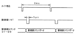
賞球制御コマンドは、主基板31から賞球制御基板37に、1バイト(8ビット:賞球制御コマンドD7〜D0)のデータとして出力される。賞球制御コマンドD7〜D0は正論理で出力される。また、賞球制御コマンドD7〜D0が出力されたときには、負論理の賞球制御INT信号が出力される。
【0131】
この実施の形態では、図19に示すように、主基板31から賞球制御コマンドD7〜D0が出力されるときに、賞球制御INT信号が5μs以上ローレベルになる。賞球制御INT信号は、賞球制御基板37において、賞球制御用CPU371の割込端子に接続されている。よって、賞球制御用CPU371は、割り込みがあると、賞球制御コマンドD7〜D0が主基板31から送出されたことを認識でき、割込処理において賞球制御コマンド受信処理を行う。
【0132】
なお、図17に示されたコマンド構成は一例であって、他の構成にしてもよい。例えば、1バイト中の上位下位を、図17に示された構成とは逆にしてもよい。また、コマンド構成は1バイト構成でなく複数バイト構成であってもよい。
【0133】
図20は、賞球制御用CPU371のメイン処理を示すフローチャートである。メイン処理では、賞球制御用CPU371は、まず、RAM領域をクリアする等の初期値設定処理を行う(ステップS701)。なお、内蔵RAMの電源バックアップされたRAM領域(バックアップRAM領域)にデータが設定されている場合には、それらの領域のクリア処理はなされない。その後、この実施の形態では、賞球制御用CPU371は、タイマ割込フラグの監視(ステップS702)の確認を行うループ処理に移行する。
【0134】
ステップS701の初期化処理では、後述する総合個数記憶および貸し玉個数記憶の値が0でない場合には、非バックアップRAM領域をクリアする。そして、賞球再開のための設定を行う。例えば、賞球中処理中フラグのセット等を行う。なお、バックアップRAM領域であっても、賞球個数に関わらない領域であるならば、それらのアドレスを指定してクリアするようにしてもよい。さらに、それら処理の他に、2ms毎に定期的にタイマ割込がかかるように賞球制御用CPU371に設けられているタイマレジスタの初期設定(タイムアウトが2msであることと繰り返しタイマが動作する設定)が行われる。すなわち、タイマ割込を能動化する処理と、タイマ割込インタバルを設定する処理とが実行される。
【0135】
従って、この実施の形態では、賞球制御用CPU371の内部タイマが繰り返しタイマ割込を発生するように設定される。この実施の形態では、繰り返し周期は2msに設定される。そして、図21に示すように、タイマ割込が発生すると、賞球制御用CPU371は、タイマ割込フラグをセットする(ステップS711)。
【0136】
賞球制御用CPU371は、ステップS702において、タイマ割込フラグがセットされたことを検出すると、タイマ割込フラグをリセットするとともに(ステップS703)、賞球制御処理を実行する(ステップS705)。以上の制御によって、この実施の形態では、賞球制御処理は2ms毎に起動されることになる。なお、この実施の形態では、タイマ割込処理ではフラグセットのみがなされ、賞球制御処理はメイン処理において実行されるが、タイマ割込処理で賞球制御処理を実行してもよい。
【0137】
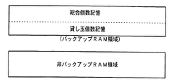
図22は、賞球制御用CPU371が内蔵するRAMの使用例を示す説明図である。この例では、バックアップRAM領域に総合個数記憶(例えば2バイト)および貸し玉個数記憶が形成されている。総合個数記憶は、主基板31の側から指示された払出個数の総数を記憶するものである。貸し玉個数記憶は、未払出の玉貸し個数を記憶するものである。なお、バックアップRAM領域には、各種フラグ類を設定するための領域もある。また、図22では、非バックアップ領域も示されているが、賞球制御用CPU371が内蔵するRAMは全て電源バックアップされていてもよい。
【0138】
図23は、割込処理による賞球制御コマンド受信処理を示すフローチャートである。主基板31からの賞球制御INT信号は賞球制御用CPU371の割込端子に入力されている。よって、主基板31からの賞球制御INT信号がオン状態になると、賞球制御用CPU371に割込がかかり、図23に示す賞球制御コマンドの受信処理が開始される。
【0139】
賞球制御コマンドの受信処理において、賞球制御用CPU371は、まず、賞球制御コマンドデータの入力に割り当てられている入力ポートから1バイトのデータを読み込む(ステップS852)。読み込んだデータが払出個数指示コマンドであれば(ステップS853)、払出個数指示コマンドで指示された個数を総合個数記憶に加算する(ステップS855)。そうでなければ、通信終了フラグをセットする(ステップS854)。なお、通信終了フラグは、この例では、払出個数指示コマンド以外のコマンドを受信したことを示すフラグである。
【0140】
以上のように、賞球制御基板37に搭載された賞球制御用CPU371は、主基板31のCPU56から送られた払出個数指示コマンドに含まれる賞球数をバックアップRAM領域(総合個数記憶)に記憶する。
【0141】
なお、賞球制御コマンドには払出個数指示コマンド以外のコマンドもあるが、図23では、それらのコマンドの受信処理は省略されている。
【0142】
図24〜図26は、賞球制御用CPU371が実行する賞球制御処理を示すフローチャートである。賞球制御処理において、賞球制御用CPU371は、現在賞球中であるか否か確認する(ステップS481)。賞球中であれば、ステップS513の賞球払出中の処理に移行する。賞球中でない場合には、玉貸し処理中であるか否か確認する(ステップS482)。玉貸し中であれば、図26に示す玉貸し中の処理に移行する。
【0143】
玉貸し中でもなければ、総合個数記憶が0であるか否か確認する(ステップS483)。総合個数記憶が0であれば、すなわち、賞球払出を開始する必要がない場合には、遊技機の外部機器としてのカードユニット50からの玉貸し要求信号であるBRQ信号がオンになっているかどうか確認する(ステップS491)。
【0144】
BRQ信号がオンになっていれば、玉貸し処理中フラグをオンし(ステップS492)、玉貸し個数カウンタに単位数を設定して(ステップS493)、EXS信号をオンする(ステップS494)。単位数は、例えば所定単位である100円で貸し出される遊技球の数(例えば25個)である。そして。玉払出装置97の下方の球振分部材311を玉貸し側に設定するために振分用ソレノイド310を駆動する(ステップS495)。また、払出モータ289をオンして(ステップS496)、図26に示す玉貸し中の処理に移行する。なお、玉貸し個数カウンタはバックアップRAM領域の貸し玉個数記憶に形成されている。また、玉貸し処理中フラグもバックアップRAM領域に設定される。
【0145】
ステップS483において、総合個数記憶が0でなければ、賞球払出を開始する処理を行う。すなわち、賞球処理中フラグをオンし(ステップS505)、玉払出装置97の下方の球振分部材311を賞球側に設定し(ステップS506)、払出モータ289をオンする(ステップS507)。そして、賞球払出中処理に移行する。なお、賞球処理中フラグは、バックアップRAM領域に設定される。
【0146】
ステップS513以降の処理は賞球払出中の処理である。賞球払出中の処理において、賞球制御用CPU371は、賞球カウントスイッチ301Aの検出出力によって遊技球の払出がなされたか否かの確認を行う。そして、1個の払出が行われたことを確認したら(ステップS513)、総合個数記憶の値を−1する(ステップS514)。また、総合個数記憶の値が0になったら(ステップS515)、払出モータ289をオフするとともに(ステップS516)、賞球処理中フラグをオフする(ステップS517)。
【0147】
総合個数記憶の内容は、遊技機の電源が断しても、所定期間電源基板910のバックアップ電源によって保存される。従って、所定期間中に電源が回復すると、賞球制御用CPU371は、総合個数記憶の内容にもとづいて賞球払出処理を継続することができる。
【0148】
賞球制御用CPU371は、電源投入時に、バックアップRAM領域のデータを確認するだけで、通常の初期設定処理を行うのか賞球中の状態を復元するのか決定できる。すなわち、簡単な判断によって、未払出賞球について賞球処理再開を行うことができる。
【0149】
なお、賞球制御用CPU371は、主基板31から指示された賞球個数を総合個数記憶で総数として管理したが、賞球数毎(例えば15個、10個、6個)に管理してもよい。例えば、賞球数毎に対応した個数カウンタを設け、払出個数指定コマンドを受信すると、そのコマンドで指定された個数に対応する個数カウンタを+1する。そして、賞球数毎の賞球払出が終了すると、対応する個数カウンタを−1する。その場合にも、各個数カウンタはバックアップRAM領域に形成される。よって、遊技機の電源が断しても、所定期間中に電源が回復すれば、賞球制御用CPU371は、各個数カウンタの内容にもとづいて賞球払出処理を継続することができる。
【0150】
図26は、賞球制御用CPU371による賞球制御処理における玉貸し中の処理を示すフローチャートである。玉貸し処理において、賞球制御用CPU371は、玉貸しカウントスイッチ301Bの検出出力によって遊技球の払出がなされたか否かの確認を行う。そして、1個の払出が行われたことを確認したら(ステップS532)、玉貸し個数カウンタの値を−1する(ステップS533)。また、玉貸し個数カウンタの値が0になったら(ステップS534)、カードユニット50に対して、玉貸し要求の受付を示すEXS信号をオフにする(ステップS535)。また、払出モータ289をオフするとともに(ステップS535)、玉貸し処理中フラグをオフする(ステップS537)。
【0151】
なお、玉貸し要求の受付を示すEXS信号をオフにした後、所定期間内に再び玉貸し要求信号であるBRQ信号がオンしたら、払出モータをオフせずに玉貸し処理を続行するようにしてもよい。すなわち、所定単位(この例では100円単位)の玉貸し処理を連続して実行するように構成することもできる。
【0152】
貸し玉個数記憶の内容は、遊技機の電源が断しても、所定期間電源基板910のバックアップ電源によって保存される。従って、所定期間中に電源が回復すると、賞球制御用CPU371は、貸し玉個数記憶の内容にもとづいて玉貸し処理を継続することができる。
【0153】
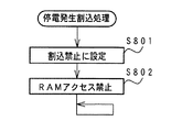
図27は、賞球制御用CPU371が第1の電源監視手段からの割込に応じて実行される停電発生割込処理を示すフローチャートである。電源基板910の電源監視用IC902が電源電圧の低下を検出すると電圧低下信号が電圧低下を示す状態となり、停電発生割込処理が開始される。停電発生割込処理において、賞球制御用CPU371は、割込禁止に設定し(ステップS801)、RAMアクセス禁止状態に設定して(ステップS802)、ループ処理に入る。すなわち、何らの処理もしない状態になる。
【0154】
従って、図16に示された電源監視用IC934からのリセット信号によって外部から動作禁止状態(システムリセット)にされる前に、内部的に動作停止状態になる。よって、電源断時に確実に賞球制御用CPU371は動作停止する。その結果、電源電圧が低下していくことに伴って生ずる可能性がある異常動作に起因するRAMの内容破壊等を確実に防止することができる。
【0155】
なお、この実施の形態では、停電発生割込処理では最終部でプログラムをループ状態にしたが、ホールト(HALT)命令を発行するように構成してもよい。また、割込処理中には他の割込がかからないような仕様のCPUを用いた場合にはステップS801の処理は不要である。
【0156】
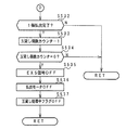
図28は、賞球制御用CPU371が電源投入時に実行する初期化処理(ステップS701)の一部を示すフローチャートである。電源が投入され、または、電源が復旧したときには、賞球制御用CPU371は、まず、バックアップRAM領域に形成されている総合個数記憶または貸し玉個数記憶の値が0でないかどうか確認する(ステップS901)。0である場合には、前回の電源オフ時に未払出賞球はなかったことになるので、通常の初期設定処理を行う。すなわち、レジスタおよび全RAM領域をクリアして(ステップS903)、スタックポインタの初期設定を行う(ステップS904)。
【0157】
総合個数記憶または貸し玉個数記憶の値が0でない場合には、アドレスを指定してレジスタと非バックアップRAM領域をクリアする(ステップS905)。そして、賞球または玉貸し再開のための設定を行う。例えば、玉貸し処理中フラグのセット等を行う(ステップS906)。なお、バックアップRAM領域であっても、賞球個数に関わらない領域であるならば、それらのアドレスを指定してクリアするようにしてもよい。
【0158】
このように、賞球制御用CPU371は、電源投入時に、バックアップRAM領域のデータを確認するだけで、通常の初期設定処理を行うのか賞球払出中または玉貸し中の状態を復元するのか決定できる。つまり、未払出の遊技球数および賞球処理中フラグと玉貸し処理中フラグとはバックアップRAMに保存されているので、賞球制御用CPU371は、賞球処理中フラグまたは玉貸し処理中フラグがセットされていれば、総合個数記憶または貸し玉個数記憶の内容に応じた処理を続行することができる。すなわち、簡単な判断によって、未払出賞球または未払出貸し玉について処理再開を行うことができる。
【0159】
上記の実施の形態では、バックアップRAM領域の貸し玉個数記憶に記憶されている玉貸しに関する情報は、玉貸し個数カウンタの値である。すなわち、1回の所定単位(この例では100円に対応する単位数:25個)における未払出遊技球数である。しかし、複数回の所定単位の全てについての未払出貸し玉数を貸し玉個数記憶に記憶してもよい。その場合、例えば、500円分の玉貸しの要求、すなわち、所定単位の5回分の玉貸し要求を、賞球制御用CPU371は、あらかじめ全て受け付け、所定単位5回分の玉貸しを行うべき旨の情報をバックアップRAM領域の貸し玉個数記憶に記憶する。
【0160】
図29は、そのような制御を実現するために、賞球制御用CPU371が実行する賞球制御処理を示すフローチャートである。この場合には、カードユニット50からのBRQ信号がオンすると(ステップS491)、玉貸し個数カウンタの値が0ならば玉貸し個数カウンタに単位数(この例では25)を設定し、玉貸し個数カウンタの値が0でなければ玉貸し回数カウンタを+1する(ステップS497)。この実施の形態では、玉貸し回数カウンタは玉貸し回数(所定単位の何回分かを示す)を計数するものであり、玉貸し個数カウンタは、各回の払出数を計数するものとして用いられる。
【0161】
さらに、賞球制御用CPU371は、EXS信号をオン状態にしてカードユニット50に要求受付を通知すると、次の回のBRQ信号のオンを許可するために直ちにEXS信号をオフにする(ステップS498)。なお、カードユニット50がEXS信号のオンオフを確実に認識できるように、ステップS498の実行前にディレイ時間をおいてもよい。
【0162】
そして、図30に示す玉貸し中の処理において、1個の払出が終了していない間、カードユニット50からの玉貸し要求信号であるBRQ信号がオンになっているかどうか確認する(ステップS545)。BRQ信号がオンになっていれば、玉貸し回数カウンタを+1して(ステップS546)、玉貸し要求の受付を示すEXS信号をオン状態にした後に(ステップS547)、EXS信号をオフにする(ステップS548)。
【0163】
また、賞球制御用CPU371は、玉貸し個数カウンタの値が0になったときには、玉貸し回数カウンタの値が0であるか否か確認し(ステップS541)、0でなければ玉貸し個数カウンタにあらためて単位数を設定するとともに(ステップS542)、玉貸し回数カウンタの値を1減らす(ステップS543)。玉貸し回数カウンタの値が0であれば、所定単位の複数分の玉貸しが全て完了したことになるので、払出モータをオフするとともに(ステップS536)、玉貸し処理中フラグをオフする(ステップS537)。
【0164】
以上のような制御によって、カードユニット50から所定回連続して玉貸し要求が出力される場合に、全ての要求が順次受け付けられる。そして、受け付けたが、その受付に対してまだ払い出しが開始されていないものについては玉貸し回数カウンタの値に保存される。
【0165】
玉貸し回数カウンタおよび玉貸し個数カウンタの値はバックアップRAM領域における貸し玉個数記憶に記憶されるので、遊技機に対する電源が断しても所定期間は保存される。そして、その所定期間内に電源が回復すれば、賞球制御用CPU371は、保存されている玉貸し回数カウンタおよび玉貸し個数カウンタの値にもとづいて玉貸し処理を続行することができる。すなわち、払出制御手段が、複数回の玉貸し要求を全て受け付けて、その後に順次玉貸し処理を実行するように構成されている場合でも、遊技者に対して玉貸しに関する不利益を与えることのない制御が実現される。
【0166】
なお、この実施の形態では、複数回の玉貸し要求の受付が開始されると同時に実際の玉貸し処理も開始されるように構成されているが、事前に複数回の玉貸し要求を全て受け付け、受付完了後に実際の玉貸し処理を開始するように構成してもよい。
【0167】
上記の実施の形態では、停電等の電源断が生じたときの電力供給停止時処理として単にRAMアクセス禁止を行っただけであるが、RAM内のデータを対象としてパリティデータを作成し、作成したパリティデータも保存するようにしてもよい。そして、電源投入時の処理において、パリティデータにもとづく確認を行い、RAM内のデータが正しく保存されていたことを確認したら、保存されているデータにもとづく賞球払出処理または玉貸し処理を続行するようにしてもよい。
【0168】
図31は、そのような電力供給停止時処理を示すフローチャートである。賞球制御用CPU371は、まず、割込禁止に設定する(ステップS801)。なお、割込処理中では他の割込がかからないような仕様のCPUを用いている場合には、ステップS801の処理は不要である。
【0169】
次いで、CPU56は、電源断フラグが既にセットされているか否か確認する(ステップS803)。電源断フラグが既にセットされていれば、以後の処理を行わない。電源断フラグがセットされていなければ、以下の電力供給停止時処理を実行する。すなわち、ステップS804からステップS810の処理を実行する。
【0170】
まず、全ての出力ポートをオフ状態にする(ステップS804)。そして、必要ならば各レジスタの内容をバックアップRAM領域に格納する(ステップS805。さらに、バックアップRAM領域のバックアップチェックデータ領域に適当な初期値を設定し(ステップS806)、初期値およびバックアップRAM領域のデータについて順次排他的論理和をとって(ステップS807)、最終的な演算値(チェックサム)をバックアップパリティデータ領域に設定する(ステップS808)。その後、電源断フラグをセットする(ステップS809)。また、RAMアクセス禁止状態にする(ステップS810)。
【0171】
次いで、賞球制御用CPU371は、ループ処理にはいる。すなわち、何らの処理もしない状態になる。最終部でプログラムをループ状態にする代わりに、ホールト(HALT)命令を発行するように構成してもよい。
【0172】
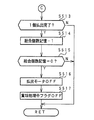
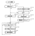
図32は、図31に示す電力供給停止時処理を行う賞球制御用CPU371が実行するメイン処理を示すフローチャートである。遊技機に対する電源が投入されると、メイン処理において、賞球制御用CPU371は、まず、停電からの復旧時であったか否か確認する(ステップS721)。停電からの復旧時であったか否かは、例えば、電源断時にバックアップRAM領域に設定される電源断フラグによって確認される。
【0173】
停電からの復旧時であった場合には、バックアップRAM領域のデータチェック(この例ではパリティチェック)を行う(ステップS723)。不測の電源断が生じた後に復旧した場合には、バックアップRAM領域のデータは保存されていたはずであるから、チェック結果は正常になる。チェック結果が正常でない場合には、内部状態を電源断時の状態に戻すことができないので、停電復旧時でない電源投入時に実行される初期化処理を実行する(ステップS724,S722)。よって、バックアップRAM領域のデータは無効化される。
【0174】
チェック結果が正常であれば、賞球制御用CPU371は、内部状態を電源断時の状態に戻すための状態復旧処理を行うとともに(ステップS725)、電源断フラグをクリアする(ステップS726)。ここでの状態復旧処理とは、例えば、バックアップRAM領域に退避されていたレジスタ値をレジスタに書き戻す処理である。
【0175】
その後、賞球制御用CPU371は、ステップS702において、タイマ割込フラグがセットされたことを検出すると、タイマ割込フラグをリセットするとともに(ステップS703)、賞球制御処理を実行する(ステップS705)。
【0176】
この実施の形態では、電力供給停止時処理において、チェックサムもバックアップRAM領域に格納され、電源投入時にチェックサムにもとづいて、保存データにもとづく賞球払出処理または玉貸し処理を行うか否か決定するので、電源復旧時の保存データにもとづく処理がさらに確実に行われる。
【0177】
以上のように、上記の各実施の形態では、賞球制御手段が、遊技機の電源時に、電源断中でも記憶内容を保持可能なバックアップRAMに玉払出装置97から貸し出されるべき遊技球の残数を特定可能に保存するための電力供給停止時処理を行うとともに、電源復旧時に、バックアップRAMに遊技球の残数を特定可能な情報が保存されている場合にはその情報にもとづいて貸出制御を続行するように構成されているので、不測の停電等の電源断が生じても、遊技者に対して払い出されない貸し玉が生ずる等の不都合が解消される。
【0178】
なお、上記の各実施の形態では、電源断時に、賞球制御手段が、遊技機の電源時に、所定の電力供給停止時処理を行ったが、そのような処理を行わなくても、未払出の遊技球数を特定可能な情報がバックアップRAMに保存されていれば、電源復帰時に、保存されている情報にもとづいて遊技球払出制御を再開することはできる。
【0179】
また、賞球制御手段が、遊技球の残数として所定単位(この例では100円)の遊技球貸出に関する残り数を保存する場合には、所定単位毎の残数が未貸出である場合に、電源復旧時に未貸出遊技球を確実に払い出すことができる。なお、所定単位の遊技球貸出に関する残り数を保存する構成は、賞球制御手段が、カードユニット50との通信に応じて所定単位の遊技球貸出処理を複数回連続して行うことが可能である場合のみならず、所定単位の払い出しが完了する毎に貸出処理を一旦停止し、その後に次の貸出要求を受け付けることが可能である場合にも適用できる。
【0180】
さらに、賞球制御手段が、カードユニット50との通信に応じて所定単位の遊技球貸出処理を複数回連続して行うことが可能であって、カードユニット50からの複数回の遊技球貸出要求の全てについて事前に(過去の受付に対する払い出しが開始されない、または開始されても完了していないときに)受付可能であり、賞球制御手段が、複数回の遊技球貸出処理にわたる全てについての未貸出の遊技球数を保存するように構成されている場合には、複数回の遊技球貸出要求の全てを事前に受け付けたとしても、受付がなされているものについては電源復旧時に未貸出遊技球を確実に払い出すことができる。
【0181】
なお、上記の各実施の形態では、記憶手段としてRAMを用いた場合を示したが、記憶手段として、電気的に書き換えが可能な記憶手段であればRAM以外のものを用いてもよい。また、上記の各実施の形態では、払出装置として、遊技球の景品払い出しと貸し出しとをともに行う玉払出装置97を用いたが、景品遊技球を払い出す払出装置と所定の遊技球を貸し出す払出装置とに分かれているものを用いてもよい。その場合、それらは同一筐体(ケース)内に設けられていてもよいし、別筐体として設置されていてもよい。
【0182】
【発明の効果】
以上のように、本発明によれば、遊技機を、遊技媒体払出要求にもとづいた遊技媒体の払出数のうち払い出しが完了していない未払出数を特定可能な情報を、電力停止中であっても少なくとも所定期間において保持可能な記憶手段を備え、払出制御マイクロコンピュータが、電力供給開始時に、記憶手段に記憶されている未払出数を特定可能な情報にもとづいて遊技媒体の払出制御を再開させることが可能であるように構成したので、遊技機に停電等による電源断状態が発生しても、遊技媒体の貸出に関して遊技者に不利益を与えることがないという効果がある。
また、貸し遊技媒体検出手段に供給される電圧よりも高い直流電圧の電源の状態を監視して、該電源の電圧が貸し遊技媒体検出手段に供給される電圧よりも高い電圧である所定電圧に低下したときに所定の検出信号を出力する電源監視手段を備え、払出制御マイクロコンピュータが、電源監視手段からの検出信号に応じて所定の電力供給停止時処理を行うように構成されている場合には、払出制御マイクロコンピュータは、電力供給停止時処理を開始すべきタイミングを容易に認識することができる。
また、電源監視手段が所定の検出信号を出力するときから少なくとも電力供給停止時処理完了後に成立するように設定された検出条件が成立したときにリセット信号を出力するリセット信号出力手段が設けられ、払出制御マイクロコンピュータは、リセット信号出力手段からのリセット信号の入力に応じて動作禁止状態とされることから、払出制御マイクロコンピュータの動作が外部からも停止されるので、電源断時により確実なデータ保存を行うことができる。
【0185】
電力供給停止時処理実行手段は、電力供給停止時処理で、記憶手段へのアクセスを防止する処理を行うように構成されている場合には、電源断時に記憶手段内のデータが破壊されることをより確実に防止できる。
【0186】
電力供給停止時処理実行手段は、電力供給停止時処理で、記憶手段の記憶内容に関連した演算の結果得られるチェックデータを記憶手段に保存する処理を行うように構成されている場合には、電力供給開始時にチェックデータにもとづいてデータが破壊されていないかどうかチェックするように構成することが可能になり、保存されるデータの信頼性を向上させることができる。
また、払出制御マイクロコンピュータは、電力供給開始時にチェックデータにもとづくチェックを行い、チェック結果が正常でなければ記憶手段に保存されている遊技媒体の未払出数に関する情報を無効化するように構成されている場合には、異常なデータにもとづいて遊技媒体貸出状態が復旧されてしまうことが防止される。
【0187】
電源監視手段からの検出信号は払出制御マイクロコンピュータの割込端子に入力され、払出制御マイクロコンピュータが、割込端子への入力にもとづいて電力供給停止時処理を実行するように構成されている場合には、ソフトウェアの負担を増大させることなく所定の電力供給停止時処理を開始することができる。
【0188】
未払出数に関する情報を保持することが可能な記憶手段が払出制御マイクロコンピュータに内蔵される場合には、記憶手段が払出制御マイクロコンピュータと一体化されることによって、コストを低減することができる。
【図面の簡単な説明】
【図1】 パチンコ遊技機を正面からみた正面図である。
【図2】 パチンコ遊技機の遊技盤を正面からみた正面図である。
【図3】 パチンコ遊技機を背面からみた背面図である。
【図4】 機構板に設置されている中間ベースユニット周りの構成を示す正面図である。
【図5】 玉払出装置を示す分解斜視図である。
【図6】 遊技制御基板(主基板)の回路構成を示すブロック図である。
【図7】 電源監視および電源バックアップのためのCPU周りの一構成例を示すブロック図である。
【図8】 電源基板の一構成例を示すブロック図である。
【図9】 主基板におけるCPUが実行するメイン処理を示すフローチャートである。
【図10】 初期化処理を示すフローチャートである。
【図11】 2msタイマ割込処理を示すフローチャートである。
【図12】 遊技制御処理を示すフローチャートである。
【図13】 停電発生NMI処理を示すフローチャートである。
【図14】 バックアップパリティデータ作成方法を説明するための説明図である。
【図15】 賞球制御基板および玉払出装置の構成要素などの賞球に関連する構成要素を示すブロック図である。
【図16】 電源監視および電源バックアップのための賞球制御用CPU周りの一構成例を示すブロック図である。
【図17】 賞球制御コマンドの構成例を示す説明図である。
【図18】 賞球制御コマンドのビット構成を示す説明図である。
【図19】 賞球制御コマンドデータの出力の様子を示すタイミング図である。
【図20】 賞球制御用CPUが実行するメイン処理を示すフローチャートである。
【図21】 賞球制御用CPUのタイマ割込処理を示すフローチャートである。
【図22】 賞球制御手段におけるRAMの一構成例を示す説明図である。
【図23】 賞球制御用CPUのコマンド受信処理を示すフローチャートである。
【図24】 賞球制御処理を示すフローチャートである。
【図25】 賞球制御処理を示すフローチャートである。
【図26】 賞球制御処理を示すフローチャートである。
【図27】 賞球制御用CPUが実行する停電発生割込処理を示すフローチャートである。
【図28】 賞球制御用CPUの初期化処理の一例を示すフローチャートである。
【図29】 賞球制御処理の他の例を示すフローチャートである。
【図30】 賞球制御処理の他の例を示すフローチャートである。
【図31】 賞球制御用CPUが実行する停電発生割込処理の他の例を示すフローチャートである。
【図32】 賞球制御用CPUが実行するメイン処理の他の例を示すフローチャートである。
【符号の説明】
1 パチンコ遊技機
31 主基板
37 賞球制御基板
50 カードユニット
56 CPU
97 玉払出装置
289 払出モータ
301A 賞球カウントスイッチ
301B 玉貸しカウントスイッチ
310 振分用ソレノイド
311 球振分部材
371 賞球制御用CPU
902,904,932,934 電源監視用IC[0001]
BACKGROUND OF THE INVENTION
The present invention relates to a gaming machine such as a pachinko gaming machine, a coin gaming machine, or a slot machine in which a game is performed according to a player's operation, and particularly, a game is performed according to a player's operation in a gaming area on a gaming board. It relates to gaming machines.
[0002]
[Prior art]
As a gaming machine, a game medium such as a game ball is launched into a game area by a launching device, and when a game medium wins a prize area such as a prize opening provided in the game area, a predetermined number of prize balls are paid out to the player. There is something to be done. The game medium is paid out by a payout mechanism.
[0003]
The payout mechanism is generally controlled by prize ball control means mounted on the prize ball control board. Since the progress of the game is controlled by game control means mounted on the main board, the number of winning balls based on winning is determined by the game control means and transmitted to the winning ball control board.
[0004]
Further, the player borrows game media and plays a game using the borrowed game media and the game media paid out in accordance with the winning. At that time, the game medium lending request from the player is received once by a lending request processing device such as a card unit, and the lending control means of the gaming machine receives the lending request from the player by communicating with the lending request processing device. A gaming machine lends a game medium in response to a lending request from a player, but there are many gaming machines that are also configured to lend balls by a payout mechanism that pays out a prize ball. Therefore, the prize ball control means and the lending control means are often constituted by an integrated payout control means (hereinafter simply referred to as prize ball control means). In general, the prize ball control means includes a payout control microcomputer.
[0005]
[Problems to be solved by the invention]
When a power failure occurs due to a power failure, etc., the game machine must be restored to its initial state (for example, the state when the game machine was first turned on that day at the amusement store). , There may be a penalty for the player. For example, when the power-off state occurs when the power-off state occurs due to a power failure or the like, while the prize ball control means has not completed the lending processing of all game media corresponding to the lending request via the lending request processing device. When the state of the gaming machine returns to the initial state, unpaid gaming media occurs, resulting in a disadvantage to the player.
[0006]
In view of the above, an object of the present invention is to provide a gaming machine that does not give a disadvantage to a player regarding lending to a gaming medium even if the gaming machine is turned off due to a power failure or the like.
[0007]
[Means for Solving the Problems]
The gaming machine according to the present invention allows a player toPredeterminedA game machine capable of playing a game, wherein a payout device capable of renting game media used in the game, and game medium lending control for paying out game media from the payout device in response to a game media loan request The payout control microcomputer, the rental game medium detection means for detecting the game medium provided in the gaming machine and paid out from the payout device, and the state of the power source of DC voltage higher than the voltage supplied to the rental game medium detection means Power supply monitoring means for monitoring and outputting a predetermined detection signal when the voltage of the power supply drops to a predetermined voltage that is higher than the voltage supplied to the rental game medium detection means;When the same DC voltage as the DC voltage monitored by the power supply monitoring means is monitored and the DC voltage becomes a detection voltage set lower than a predetermined voltage when the power supply monitoring means outputs a predetermined detection signal. Reset signal output means for outputting a reset signal for prohibiting the operation of the payout control microcomputer;Retains information that can identify the number of unpaid games that have not been paid out of the number of paid-out game media based on a game media lending request, at least for a specified period even when power supply to the gaming machine is stopped The payout control microcomputer includes a subtracting means for executing a process of subtracting the number of unpaid when the detection output is output from the rental game medium detecting means, and a predetermined detection from the power supply monitoring means. In response to the signal, the operation of the dispensing device is stopped, and the power supply stop time processing execution means for executing the power supply stop time processing for storing the power supply stop information indicating that the power supply is stopped in the storage means, and the power On the condition that the power supply stop information is stored in the storage means when the supply is started, based on information that can specify the number of unpaid items stored in the storage means. Including a recovery means for resuming the payout control of game media TeThe reset signal output means outputs a reset signal when the detection condition set so as to be satisfied at least after completion of the power supply stop process from when the power monitoring means outputs a predetermined detection signal, and pays out. The control microcomputer is in an operation-prohibited state in response to the input of the reset signal from the reset signal output means.It is characterized by that.
[0010]
The processing execution means at the time of power supply stop isProcessing when power supply is stoppedso,Processing to prevent access to storage meansI doIt may be configured as follows.
[0011]
The processing execution means at the time of power supply stop isProcessing when power supply is stoppedsoProcessing for storing check data obtained as a result of calculation related to the storage contents of the storage means in the storage meansI doIt may be configured as follows.
Further, the payout control microcomputer is configured to perform a check based on the check data at the start of power supply, and to invalidate the information regarding the number of unpaid game media stored in the storage means if the check result is not normal. It may be.
[0012]
ElectricThe detection signal from the source monitoring means is input to the interrupt terminal of the payout control microcomputer, and the payout control microcomputer may be configured to execute the power supply stop process based on the input to the interrupt terminal. Good.
[0013]
The storage means that can hold information that can specify the number of unpaid out for at least a predetermined period is payout control.MicrocomputerInBuilt-inIt may be a configuration. That is, the storage unit may be, for example, a memory (RAM) built in the microcomputer.
[0017]
DETAILED DESCRIPTION OF THE INVENTION
Hereinafter, an embodiment of the present invention will be described with reference to the drawings.
First, the overall configuration of a pachinko gaming machine that is an example of a gaming machine will be described. 1 is a front view of the
[0018]
As shown in FIG. 1, the
[0019]
Near the center of the
[0020]
An open / close plate 20 that is opened by a
[0021]
The
[0022]
In this example, a
[0023]
The
[0024]
The hit ball fired from the hit ball launching device enters the
[0025]
The rotation of the image in the
[0026]
When the combination of images in the
[0027]
Next, the structure of the back surface of the
On the back surface of the
[0028]
The
[0029]
FIG. 3 is a rear view of the game board of the
[0030]
In order to perform prize ball payout control, signals from a winning opening switch (not shown), the
[0031]
Next, the configuration of the intermediate base unit installed on the
[0032]
A
[0033]
The ball break switches 187a and 187b are locked by a locking piece 188 at a position where it can be detected that 27 to 28 premium balls are present in the
[0034]
The central portion of the
[0035]
Below the
[0036]
FIG. 5 is an exploded perspective view of the
[0037]
As shown in FIG. 5, the
[0038]
The
[0039]
In addition, below the ball
[0040]
[0041]
A recess is formed at the tip of the
[0042]
In other words, the payout motor position sensor including the
[0043]
When the dispensing
[0044]
As shown in FIG. 4, a
[0045]
As described above, by providing the
[0046]
FIG. 6 is a block diagram illustrating an example of a circuit configuration in the
[0047]
Further, according to the data given from the basic circuit 53, the jackpot information indicating the occurrence of the jackpot, the effective starting information indicating the number of starting winning balls used for starting the image display of the
[0048]
The basic circuit 53 includes a
[0049]
Further, the
In addition, although there is switch information input to the
[0050]
A ball hitting device for hitting and launching a game ball is driven by a
[0051]
FIG. 7 is a block diagram showing a configuration example around the CPU 56 for power supply monitoring and power supply backup. As shown in FIG. 7, the voltage drop signal from the first power supply monitoring circuit (first power supply monitoring means) mounted on the power supply board is connected to the non-maskable interrupt terminal (NMI terminal) of the CPU 56. Yes. The first power supply monitoring circuit is a circuit that monitors the voltage of any one of the various DC power supplies used by the gaming machine and detects a power supply voltage drop. Therefore, the CPU 56 can confirm the occurrence of power interruption by the interrupt process.
[0052]
In the
[0053]
A second power
[0054]
Therefore, in this example, the first detection condition that the first power supply monitoring means outputs the detection signal is that the + 30V power supply voltage has dropped to + 21V, and the second power supply monitoring means outputs the detection signal. The second detection condition to be performed is that the + 30V power supply voltage is lowered to + 9V. However, the voltage value used here is an example, and other values may be used.
[0055]
In such a configuration, since the same voltage is monitored, the difference between the timing at which the first voltage monitoring circuit outputs the voltage drop signal and the timing at which the second voltage monitoring circuit outputs the voltage drop signal is desired. Can be reliably set in a predetermined period. The desired predetermined period is a period from when the power supply stop process is started in response to the voltage drop signal from the first power supply monitoring circuit until the power supply stop process is reliably completed.
[0056]
The voltage drop signal from the second power
[0057]
Note that the reset IC 651 of the initial reset circuit 65 sets the output signal to a high level when the + 5V power supply voltage becomes a predetermined value or more when the gaming machine is turned on and the voltage of the + 5V power supply rises. That is, the initial reset signal is turned off.
[0058]
While power is not supplied from the + 5V power source that is the driving power source of the CPU 56 or the like, at least a part of the RAM is backed up by the backup power source supplied from the power supply board, and the contents are preserved even if the power to the gaming machine is cut off. The When the + 5V power supply is restored, a reset signal is issued from the initial reset circuit 65, so that the CPU 56 returns to a normal operation state. At that time, since necessary data is backed up, it is possible to return to the gaming state at the time of the power failure when recovering from the power failure.
[0059]
FIG. 8 is a block diagram illustrating a configuration example of the
[0060]
The transformer 911 converts AC voltage from the AC power source into 24V. The AC 24V voltage is output to the connector 915. The rectifier circuit 912 also generates a DC voltage of +30 V from AC 24 V and outputs it to the DC-DC converter 913 and the connector 915. The DC-DC converter 913 generates + 21V, + 12V, and + 5V and outputs them to the connector 915. The connector 915 is connected to, for example, a relay board, and power of a voltage necessary for each electric component control board and the mechanism component is supplied from the relay board. Note that a
[0061]
The + 5V line from the DC-DC converter 913 branches to form a backup + 5V line. A large-capacitance capacitor 916 is connected between the backup + 5V line and the ground level. Capacitor 916 has power so that the storage state can be maintained with respect to the backup RAM of the electrical component control board when the power supply to the gaming machine is cut off (RAM that is backed up by power, that is, storage means that can be in the storage content storage state). Backup power supply. Further, a
[0062]
A battery that can be charged from a + 5V power supply may be used as the backup power supply. In the case of using a battery, a rechargeable battery is used in which the capacity disappears when a state in which no power is supplied from the +5 V power source continues for a predetermined time.
[0063]
The
[0064]
The predetermined value for the
[0065]
Further, since the
[0066]
In the configuration shown in FIG. 8, the detection output (voltage drop signal) of the
[0067]
Next, the operation of the gaming machine will be described.
FIG. 9 is a flowchart showing main processing executed by the CPU 56 on the
[0068]
If it is time to recover from a power failure, a data check (parity check in this example) of the backup RAM area is performed (step S3). In the case of recovery after an unexpected power failure, the data in the backup RAM area should have been saved, so the check result is normal. If the check result is not normal, the internal state cannot be returned to the state when the power is cut off, and therefore an initialization process that is executed when the power is turned on not when the power failure is restored is executed (steps S4 and S2).
[0069]
If the check result is normal, the CPU 56 performs a game state recovery process for returning the internal state to the state at the time of power-off (step S5) and clears the power-off flag (step S6).
[0070]
If it is not time to recover from a power failure, the CPU 56 executes normal initialization processing (steps S1 and S2). Thereafter, in the main process, the process proceeds to a loop process in which the monitoring of the timer interrupt flag (step S6) is confirmed. In the loop, display random number update processing (step S7) is also executed.
[0071]
Here, it is confirmed in step S1 whether or not the recovery from the power failure, and if the recovery from the power failure, the parity check is performed. First, the parity check is performed and the check result is not normal. If it is determined that the power is not recovered from the power failure, the initialization process of step S2 is executed. If the check result is normal, the game state return process may be performed. That is, it may be determined whether or not recovery from a power failure is made based on the result of the parity check.
[0072]
Further, when determining whether or not to execute the power failure recovery processing, that is, when determining whether or not to restore the gaming state, according to the special process flag or the like in the stored RAM data or the start winning memory number data, If it is confirmed that the gaming machine is in a game standby state (no special symbol change, no big hit game, no probable change, and no start winning memory), the game state restoration process is not performed. An initialization process may be executed.
[0073]
In the normal initialization process, as shown in FIG. 10, after the register and RAM clear process (step S2a) and the necessary initial value setting process (step S2b) are performed, a timer allocation is periodically performed every 2 ms. Initial setting of the timer register provided in the CPU 56 (setting that the time-out is 2 ms and the timer repeatedly operates) is performed so as to cause a delay (step S2c). That is, in step S2c, processing for activating a timer interrupt and processing for setting a timer interrupt interval are executed.
[0074]
Therefore, in this embodiment, the internal timer of the CPU 56 is set to repeatedly generate a timer interrupt. In this embodiment, the repetition period is set to 2 ms. Then, as shown in FIG. 11, when a timer interrupt occurs, the CPU 56 sets a timer interrupt flag (step S11).
[0075]
When detecting that the timer interrupt flag is set in step S8, the CPU 56 resets the timer interrupt flag (step S9) and executes a game control process (step S10). With the above control, in this embodiment, the game control process is started every 2 ms. In this embodiment, only the flag is set in the timer interrupt process, and the game control process is executed in the main process, but the game control process may be executed in the timer interrupt process.
[0076]
FIG. 12 is a flowchart showing the game control process of step S10. In the game control process, the CPU 56 first performs a process of setting a display control command sent to the display control board 80 in a predetermined area of the RAM 55 (display control data setting process: step S21), and then displays the display control command. An output process is performed (display control data output process: step S22).
[0077]
Next, a process of outputting the contents of the storage area for various output data to each output port is performed (data output process: step S23). Also, output data setting processing is performed for setting output data such as jackpot information, start information, probability variation information, etc., output to the hall management computer in the storage area (step S24). Further, various abnormality diagnosis processes are performed by the self-diagnosis function provided in the
[0078]
Next, a process of updating each counter indicating each determination random number such as a big hit determination random number used for game control is performed (step S26).
[0079]
Further, the CPU 56 performs special symbol process processing (step S27). In the special symbol process control, corresponding processing is selected and executed according to a special symbol process flag for controlling the
[0080]
Further, the CPU 56 inputs the states of the
[0081]
Further, the CPU 56 performs signal processing with the prize ball control board 37 (step S31). That is, when a predetermined condition is satisfied, a prize ball control command is output to the prize
[0082]
As described above, the main process includes a process for determining whether or not to shift to the game control process, and the timer control process based on the timer interrupt periodically generated by the internal timer of the CPU 56 is used for the game control process. Since a flag for determining whether or not to shift is set, all the game control processes are executed reliably. In other words, until all the game control processes are executed, it is not determined whether or not to shift to the next game control process, so it is guaranteed that all the processes in the game control process are completed. ing.
[0083]
Conventional general game control processing is forcibly returned to the initial state by an external interrupt that occurs periodically. If it demonstrates in accordance with the example shown by FIG. 12, for example, even if it was during the process of step S31, it was forcibly returned to the process of step S21. In other words, there is a possibility that the next game control process will be started before all the processes in the game control process are completed.
[0084]
Here, the game control process executed by the CPU 56 of the
[0085]
FIG. 13 is a flowchart showing an example of a power failure occurrence NMI process executed in response to the NMI based on the voltage drop signal from the first power supply monitoring circuit of the
[0086]
Note that the processing in step S41 is not necessary when a CPU having a specification that does not cause other interrupts during the interrupt processing is used.
[0087]
Next, the CPU 56 checks whether or not the power-off flag has already been set (step S42). If the power-off flag is already set, the subsequent processing is not performed. If the power-off flag is not set, the following power supply stop process is executed. That is, the processing from step S43 to step S49 is executed.
[0088]
First, all output ports are turned off (step S43). If necessary, the contents of each register are stored in the backup RAM area (step S44). Further, an appropriate initial value is set in the backup check data area of the backup RAM area (step S45), the exclusive value is sequentially obtained for the initial value and the data in the backup RAM area (step S46), and the final calculation value is obtained. Is set in the backup parity data area (step S47). Thereafter, the power-off flag is set (step S48). Further, the RAM access is prohibited (step S49). When the power supply voltage is lowered, the level of various signal lines may become unstable and the contents of the RAM may be altered, but if the RAM access is prohibited in this manner, the data in the backup RAM will be altered. There is no.
[0089]
Next, the CPU 56 enters a loop process. That is, no processing is performed. Therefore, the operation is internally stopped before the operation is prohibited from the outside by the reset signal from the
[0090]
In this embodiment, in the power failure occurrence NMI processing, the program is looped at the final part, but a halt (HALT) instruction may be issued.
[0091]
Further, as described above, the power-off flag that is set before the RAM access is prohibited is used when determining whether or not to recover from a power failure when the power is turned on. Further, the processing of steps S41 to S49 is completed before the second power supply monitoring unit generates the voltage drop signal. In other words, the detection voltages of the first voltage monitoring means and the second voltage monitoring means are set so that the second power supply monitoring means is completed before generating the voltage drop signal.
[0092]
In this embodiment, the power-off flag is confirmed at the start of the power supply stop process. When the power-off flag is already set, the power supply stop process is not executed. As described above, the power-off flag is a flag indicating that the power supply stop process has been completed. Therefore, for example, even if NMI occurs again for some reason in a loop waiting for reset, the power supply stop process is not repeatedly executed.
[0093]
However, if a CPU with specifications that do not cause other interrupts during interrupt processing is used, the determination in step S42 is not necessary.
[0094]
FIG. 14 is an explanatory diagram for explaining a backup parity data creation method. However, in the example shown in FIG. 14, the size of the data in the backup data RAM area is 3 bytes for simplicity. In the power failure generation process based on the power supply voltage drop, as shown in FIG. 14A, initial data (00H in this example) is set in the backup check data area. Next, an exclusive logical sum of “00H” and “F0H” is taken, and an exclusive logical sum of “16H” is obtained. Further, an exclusive OR of the result and “DFH” is taken. Then, the result (“39H” in this example) is set in the backup parity data area.
[0095]
When the power is turned on again, parity diagnosis is performed in the power failure recovery process. FIG. 14B is an explanatory diagram showing an example of parity diagnosis. If all the data in the backup area is stored as it is, data as shown in FIG. 14A is set in the backup area when the power is turned on again.
[0096]
In the processing of step S51, the CPU 56 sequentially performs exclusive OR for each data in the backup data area using the data (in this example, “39H”) set in the backup parity data area in the backup RAM area as initial data. Process. If all the data in the backup area is stored as it is, the final calculation result matches “00H”, that is, the data set in the backup check data area. If a bit error has occurred in the data in the backup RAM area, the final calculation result is not “00H”.
[0097]
Therefore, the CPU 56 compares the final calculation result with the data set in the backup check data area, and if they match, the parity diagnosis is normal. If they do not match, the parity diagnosis is abnormal.
[0098]
As described above, in this embodiment, the game control means is provided with a storage means (a backup RAM in this example) that is backed up for a predetermined period even when the power of the gaming machine is cut off. The CPU 56 (specifically, a program executed by the CPU 56) is configured to perform a game state recovery process (step S5) for recovering the game state based on the backup data if the storage means is in the backup state.
[0099]
In this embodiment, the first power supply monitoring means is mounted on the
[0100]
Then, the CPU 56 enters the loop state after executing the power failure generation processing (processing when the power supply is stopped) based on the voltage drop signal from the first power monitoring means (power monitoring IC 902). Will enter the reset state. That is, the operation of the CPU 56 is completely stopped. In the loop state, the + 5V power supply voltage value gradually decreases and the input / output state becomes indefinite. However, since the CPU 56 is in the reset state, the abnormal operation based on the indefinite data is prevented.
[0101]
Thus, in this embodiment, the CPU 56 enters the loop state in response to the detection output input from the first power supply monitoring means, and the system in response to the detection output input from the second power supply monitoring means. Since it is configured to be reset, it is possible to reliably store data when the power is turned off, and to prevent a disadvantage from being brought to the player.
[0102]
In this embodiment, the power
[0103]
Further, the first power supply monitoring means may be mounted on the
[0104]
In the above embodiment, the CPU 56 detects the first voltage drop signal from the power supply board (voltage drop signal from the first power supply monitoring means) via the non-maskable interrupt terminal (NMI terminal). However, the first voltage drop signal may be introduced to the maskable interrupt terminal (IRQ terminal). In that case, a power supply stop process is executed in the interrupt process (IRQ process). Further, the first voltage drop signal from the power supply board may be detected via the input port. In that case, the input port is monitored in the main process.
[0105]
Further, when detecting the first voltage drop signal from the power supply board via the IRQ terminal, the IRQ interrupt mask is set at the start of the game control process of step S10 of the main process, and the IRQ is set at the end of the game control process. The interrupt mask may be canceled. By doing so, an interruption is applied before and after the start of the game control process, and the game control process is not interrupted. Therefore, the command transmission is not interrupted when the prize ball control command is sent to the prize
[0106]
FIG. 15 is a block diagram showing components related to game ball payout, such as components of the prize
[0107]
A detection signal from the ball break switch 187 (187a, 187b) is input to the I / O port 57 of the
[0108]
The CPU 56 of the
[0109]
That is, in this embodiment, the firing stop command is included in the prize ball control command and output from the
[0110]
Further, a detection signal from the prize ball count switch 301 </ b> A is also input to the I / O port 57 of the
[0111]
When there is a prize, a prize ball control command indicating the prize ball start is input to the prize
[0112]
Furthermore, a
[0113]
The prize
[0114]
Further, the detection signal of the prize
[0115]
A card unit control microcomputer is mounted on the
[0116]
A ball lending switch signal and a return switch signal are given from the
[0117]
When the power of the
[0118]
If the EXS signal is turned on and then turned off, the
[0119]
As described above, all signals from the
[0120]
In this embodiment, a case where a
[0121]
FIG. 16 is a block diagram showing a configuration example around the prize
[0122]
While power is not supplied from the + 5V power source that is the driving power source of the prize
[0123]
In the prize
[0124]
In the configuration shown in FIG. 16, a second power supply monitoring circuit 933 is mounted on the winning
[0125]
In this example, the first detection condition for the first power supply monitoring means to output the detection signal is that the + 30V power supply voltage has dropped to + 21V, and the second power supply monitoring means outputs the detection signal. For example, the second detection condition is that the + 30V power supply voltage is reduced to + 9V. However, the voltage value used here is an example, and other values may be used.
[0126]
The voltage drop signal from the second power supply monitoring circuit 933 is logically summed with the initial reset signal from the initial reset circuit 935 and then input to the reset terminal of the winning
[0127]
FIG. 17 is an explanatory diagram illustrating an example of a bit configuration of a prize ball control command transmitted from the
[0128]
As shown in FIG. 18, if
[0129]
The ball break designation command whose
[0130]
The prize ball control command is output as data of 1 byte (8 bits: prize ball control commands D7 to D0) from the
[0131]
In this embodiment, as shown in FIG. 19, when a prize ball control command D7 to D0 is output from the
[0132]
Note that the command configuration shown in FIG. 17 is an example, and other configurations may be used. For example, the upper and lower order in one byte may be reversed from the configuration shown in FIG. Further, the command configuration may be a multi-byte configuration instead of a 1-byte configuration.
[0133]
FIG. 20 is a flowchart showing main processing of the prize
[0134]
In the initialization process in step S701, the non-backup RAM area is cleared if the values of the total number storage and the lending ball number storage described later are not 0. Then, settings for restarting the prize ball are made. For example, an in-price ball processing flag is set. Even if it is a backup RAM area, if it is an area not related to the number of winning balls, it may be cleared by designating those addresses. In addition to these processes, the timer register provided in the prize
[0135]
Therefore, in this embodiment, the internal timer of the winning
[0136]
When detecting that the timer interrupt flag has been set in step S702, the prize
[0137]
FIG. 22 is an explanatory diagram showing an example of use of the RAM built in the prize
[0138]
FIG. 23 is a flowchart showing a prize ball control command reception process by an interrupt process. The prize ball control INT signal from the
[0139]
In the prize ball control command reception process, the prize
[0140]
As described above, the prize
[0141]
The prize ball control command includes commands other than the payout number instruction command, but in FIG. 23, reception processing of these commands is omitted.
[0142]
24 to 26 are flowcharts showing a prize ball control process executed by the prize
[0143]
If the ball is not being loaned, it is checked whether the total number storage is 0 (step S483). If the total number storage is 0, that is, if it is not necessary to start paying out a prize ball, is the BRQ signal that is a ball lending request signal from the
[0144]
If the BRQ signal is on, the ball lending process flag is turned on (step S492), the unit number is set in the ball lending number counter (step S493), and the EXS signal is turned on (step S494). The number of units is, for example, the number (for example, 25) of game balls lent out at a predetermined unit of 100 yen. And then. In order to set the
[0145]
In step S483, if the total number storage is not 0, a process of starting a prize ball payout is performed. That is, the prize ball processing flag is turned on (step S505), the
[0146]
The process after step S513 is a process during payout of a prize ball. In the process of paying out a prize ball, the prize
[0147]
The contents of the total number storage are saved by the backup power source of the
[0148]
When the power is turned on, the prize
[0149]
The prize
[0150]
FIG. 26 is a flowchart showing a ball lending process in the prize ball control process by the prize
[0151]
After turning off the EXS signal indicating acceptance of a ball lending request, if the BRQ signal, which is a ball lending request signal, is turned on again within a predetermined period, the ball lending process is continued without turning off the payout motor. Also good. In other words, the ball lending process of a predetermined unit (100 yen unit in this example) can be continuously executed.
[0152]
The contents of the rental ball number storage are saved by the backup power source of the
[0153]
FIG. 27 is a flowchart showing a power failure occurrence interrupt process executed by the prize
[0154]
Therefore, before the operation is prohibited (system reset) from the outside by the reset signal from the power monitoring IC 934 shown in FIG. Therefore, the winning
[0155]
In this embodiment, in the power failure occurrence interrupt process, the program is looped at the final part, but a halt (HALT) instruction may be issued. Further, when a CPU having a specification that does not cause other interrupts during the interrupt process is used, the process of step S801 is not necessary.
[0156]
FIG. 28 is a flowchart showing a part of the initialization process (step S701) executed by the prize
[0157]
If the value of the total number storage or the lending ball number storage is not 0, an address is designated and the register and the non-backup RAM area are cleared (step S905). Then, a setting for resuming the lending of the prize balls or balls is performed. For example, a ball lending process flag is set (step S906). Even if it is a backup RAM area, if it is an area not related to the number of winning balls, it may be cleared by designating those addresses.
[0158]
In this way, the prize
[0159]
In the above embodiment, the information related to the ball lending stored in the lending ball number storage in the backup RAM area is the value of the ball lending number counter. That is, the number of unpaid game balls in one predetermined unit (in this example, the number of units corresponding to 100 yen: 25). However, the number of unpaid lending balls for all of the predetermined units may be stored in the lending ball number storage. In that case, for example, the prize
[0160]
FIG. 29 is a flowchart showing a prize ball control process executed by the prize
[0161]
Further, when the prize
[0162]
Then, in the ball lending process shown in FIG. 30, while one payout is not completed, it is confirmed whether or not the BRQ signal, which is a ball lending request signal from the
[0163]
In addition, when the value of the ball lending number counter becomes 0, the prize
[0164]
By the control as described above, when the ball lending request is continuously output from the card unit 50 a predetermined number of times, all the requests are sequentially accepted. Then, those that have been accepted but have not yet started to be paid out are saved in the value of the ball lending counter.
[0165]
Since the value of the ball lending number counter and the ball lending number counter is stored in the lending ball number storage in the backup RAM area, it is stored for a predetermined period even when the power to the gaming machine is cut off. If the power is restored within the predetermined period, the winning
[0166]
In this embodiment, the configuration is such that the actual ball lending process is started at the same time as the acceptance of a plurality of ball lending requests is started, but all the ball lending requests are accepted in advance. The actual ball lending process may be started after completion of the reception.
[0167]
In the above embodiment, the RAM access is simply prohibited as the power supply stop process when a power interruption such as a power failure occurs, but the parity data is created and created for the data in the RAM. Parity data may also be stored. Then, at the time of power-on processing, confirmation based on the parity data is performed, and if it is confirmed that the data in the RAM is correctly stored, the winning ball payout processing or ball lending processing based on the stored data is continued. You may do it.
[0168]
FIG. 31 is a flowchart showing such a power supply stop process. First, the winning
[0169]
Next, the CPU 56 checks whether or not the power-off flag has already been set (step S803). If the power-off flag is already set, the subsequent processing is not performed. If the power-off flag is not set, the following power supply stop process is executed. That is, the processing from step S804 to step S810 is executed.
[0170]
First, all output ports are turned off (step S804). If necessary, the contents of each register are stored in the backup RAM area (step S805. Further, an appropriate initial value is set in the backup check data area of the backup RAM area (step S806), and the initial value and the backup RAM area are stored. The data is sequentially exclusive-ORed (step S807), and the final operation value (checksum) is set in the backup parity data area (step S808), and then the power-off flag is set (step S809). Further, the RAM access is prohibited (step S810).
[0171]
Next, the prize
[0172]
FIG. 32 is a flowchart showing a main process executed by the winning
[0173]
If it is at the time of recovery from a power failure, data check of the backup RAM area (parity check in this example) is performed (step S723). In the case of recovery after an unexpected power failure, the data in the backup RAM area should have been saved, so the check result is normal. If the check result is not normal, the internal state cannot be returned to the state at the time of power-off, and therefore initialization processing that is executed at the time of power-on that is not at the time of power failure recovery is executed (steps S724 and S722). Therefore, the data in the backup RAM area is invalidated.
[0174]
If the check result is normal, the winning
[0175]
Thereafter, when it is detected in step S702 that the timer interrupt flag has been set, the prize
[0176]
In this embodiment, in the power supply stop process, the checksum is also stored in the backup RAM area, and it is determined whether or not to perform a prize ball payout process or a ball lending process based on the stored data based on the checksum when the power is turned on. Therefore, the processing based on the stored data when the power is restored is further reliably performed.
[0177]
As described above, in each of the above embodiments, when the gaming machine is powered on, the remaining number of game balls to be lent from the
[0178]
In each of the above embodiments, when the power is cut off, the prize ball control means performs a predetermined power supply stop process when the gaming machine is powered. If the information that can specify the number of game balls is stored in the backup RAM, the game ball payout control can be resumed based on the stored information when the power is restored.
[0179]
Further, when the prize ball control means stores the remaining number relating to the gaming ball lending of a predetermined unit (100 yen in this example) as the remaining number of gaming balls, the remaining number per predetermined unit is not lent out. , It is possible to reliably pay out unrented game balls when power is restored. Note that the configuration in which the remaining number related to a predetermined unit of game ball lending is stored allows the prize ball control means to continuously perform the predetermined unit of game ball lending processing a plurality of times in response to communication with the
[0180]
Further, the prize ball control means can continuously perform a predetermined unit of game ball lending processing a plurality of times in response to communication with the
[0181]
In each of the above embodiments, the case where the RAM is used as the storage means has been described. However, as the storage means, any storage means other than the RAM may be used as long as it is an electrically rewritable storage means. In each of the above embodiments, the
[0182]
【The invention's effect】
As described above, according to the present invention, information indicating the number of game media payouts that have not been paid out of the number of game media payouts based on the game media payout request can be identified by the gaming machine during power outage. However, it is provided with storage means that can be held for at least a predetermined period, and the payout control microcomputer restarts payout control of the game medium based on information that can specify the number of unpaid numbers stored in the storage means at the start of power supply. Therefore, even if a power-off state due to a power failure or the like occurs in the gaming machine, there is an effect that the player is not disadvantaged regarding the rental of the game medium.
Further, the state of the power source having a DC voltage higher than the voltage supplied to the rental game medium detecting means is monitored, and the voltage of the power source is set to a predetermined voltage that is higher than the voltage supplied to the rental game medium detecting means. Power supply monitoring means for outputting a predetermined detection signal when the voltage drops, and the payout control microcomputer is configured to perform predetermined power supply stop processing in response to the detection signal from the power supply monitoring means The payout control microcomputer can easily recognize the timing at which the power supply stop process should be started.
Further, there is provided a reset signal output means for outputting a reset signal when a detection condition set to be satisfied at least after completion of the power supply stop process from when the power monitoring means outputs a predetermined detection signal, Since the payout control microcomputer is disabled in response to the input of the reset signal from the reset signal output means, the operation of the payout control microcomputer is also stopped from the outside. Can be saved.
[0185]
The processing execution means at the time of power supply stop isProcessing when power supply is stoppedso,Processing to prevent access to storage meansI doIn such a configuration, it is possible to more reliably prevent the data in the storage unit from being destroyed when the power is turned off.
[0186]
The processing execution means at the time of power supply stop isProcessing when power supply is stoppedsoProcessing for storing check data obtained as a result of calculation related to the storage contents of the storage means in the storage meansI doIf configured toPower supply startedIt can be configured to check whether the data has been destroyed based on the check data from time to time, and the reliability of the stored data can be improved.
Further, the payout control microcomputer is configured to perform a check based on the check data at the start of power supply, and to invalidate the information regarding the number of unpaid game media stored in the storage means if the check result is not normal. In such a case, it is possible to prevent the gaming medium lending state from being restored based on abnormal data.
[0187]
ElectricWhen the detection signal from the source monitoring means is input to the interrupt terminal of the payout control microcomputer, and the payout control microcomputer is configured to execute the power supply stop process based on the input to the interrupt terminal The predetermined power supply stop process can be started without increasing the software load.
[0188]
A storage means that can hold information on the number of unpaid items is payout controlMicrocomputerInBuilt-inIf the storage meansMicrocomputerBy being integrated withCoStrikes can be reduced.
[Brief description of the drawings]
FIG. 1 is a front view of a pachinko gaming machine as viewed from the front.
FIG. 2 is a front view of a game board of a pachinko gaming machine as viewed from the front.
FIG. 3 is a rear view of the pachinko gaming machine as viewed from the back.
FIG. 4 is a front view showing a configuration around an intermediate base unit installed on a mechanism plate.
FIG. 5 is an exploded perspective view showing a ball dispensing device.
FIG. 6 is a block diagram showing a circuit configuration of a game control board (main board).
FIG. 7 is a block diagram showing an example of a configuration around a CPU for power monitoring and power backup.
FIG. 8 is a block diagram illustrating a configuration example of a power supply board.
FIG. 9 is a flowchart showing main processing executed by a CPU on the main board.
FIG. 10 is a flowchart showing initialization processing.
FIG. 11 is a flowchart showing a 2 ms timer interrupt process.
FIG. 12 is a flowchart showing a game control process.
FIG. 13 is a flowchart showing a power failure occurrence NMI process.
FIG. 14 is an explanatory diagram for explaining a backup parity data creation method;
FIG. 15 is a block diagram showing components related to a prize ball, such as components of a prize ball control board and a ball payout device.
FIG. 16 is a block diagram showing an example of the configuration around a prize ball control CPU for power supply monitoring and power supply backup.
FIG. 17 is an explanatory diagram showing a configuration example of a prize ball control command.
FIG. 18 is an explanatory diagram showing a bit configuration of a prize ball control command.
FIG. 19 is a timing chart showing a state of outputting prize ball control command data.
FIG. 20 is a flowchart showing main processing executed by a prize ball control CPU.
FIG. 21 is a flowchart showing a timer interrupt process of a prize ball control CPU.
FIG. 22 is an explanatory diagram showing a configuration example of a RAM in the winning ball control means.
FIG. 23 is a flowchart showing command reception processing of a prize ball control CPU;
FIG. 24 is a flowchart showing a prize ball control process.
FIG. 25 is a flowchart showing a prize ball control process.
FIG. 26 is a flowchart showing a prize ball control process.
FIG. 27 is a flowchart showing a power failure occurrence interrupt process executed by the winning ball control CPU.
FIG. 28 is a flowchart illustrating an example of initialization processing of a prize ball control CPU.
FIG. 29 is a flowchart showing another example of the winning ball control process.
FIG. 30 is a flowchart showing another example of the winning ball control process.
FIG. 31 is a flowchart showing another example of a power failure occurrence interrupt process executed by the winning ball control CPU.
FIG. 32 is a flowchart showing another example of the main process executed by the winning ball control CPU.
[Explanation of symbols]
1 Pachinko machine
31 Main board
37 prize ball control board
50 card units
56 CPU
97 Ball dispenser
289 Dispensing motor
301A Prize ball count switch
301B Ball lending count switch
310 Solving solenoid
311 Ball sorting member
371 CPU for prize ball control
902,904,932,934 IC for power supply monitoring
Claims (8)
遊技に用いられる遊技媒体を貸し出すことが可能な払出装置と、
遊技媒体貸出要求に応じて前記払出装置から遊技媒体を払い出す遊技媒体貸出制御を行う払出制御マイクロコンピュータと、
遊技機に設けられ前記払出装置から払い出された遊技媒体を検出する貸し遊技媒体検出手段と、
前記貸し遊技媒体検出手段に供給される電圧よりも高い直流電圧の電源の状態を監視して、該電源の電圧が前記貸し遊技媒体検出手段に供給される電圧よりも高い電圧である所定電圧に低下したときに所定の検出信号を出力する電源監視手段と、
前記電源監視手段が監視する直流電圧と同一の直流電圧を監視し、該直流電圧が、前記電源監視手段が所定の検出信号を出力するときの所定電圧よりも低く設定された検出電圧になったときに前記払出制御マイクロコンピュータの動作を禁止させるためのリセット信号を出力するリセット信号出力手段と、
遊技媒体貸出要求にもとづいた遊技媒体の払出数のうち払い出しが完了していない未払出数を特定可能な情報を、遊技機への電力供給が停止されたときであっても少なくとも所定期間において保持可能な記憶手段とを備え、
前記払出制御マイクロコンピュータは、
前記貸し遊技媒体検出手段から検出出力が出力されたときに前記未払出数を減算する処理を実行する減算手段と、
前記電源監視手段からの所定の検出信号に応じて、前記払出装置の動作を停止させるとともに、電力供給が停止したことを示す電力供給停止情報を前記記憶手段に格納する電力供給停止時処理を実行する電力供給停止時処理実行手段と、
電力供給が開始されたときに、前記記憶手段に前記電力供給停止情報が保存されていたことを条件に、前記記憶手段に記憶されている未払出数を特定可能な情報にもとづいて遊技媒体の払出制御を再開させる復旧手段とを含み、
前記リセット信号出力手段は、前記電源監視手段が前記所定の検出信号を出力するときから少なくとも前記電力供給停止時処理完了後に成立するように設定された検出条件が成立したときに前記リセット信号を出力し、
前記払出制御マイクロコンピュータは、前記リセット信号出力手段からの前記リセット信号の入力に応じて動作禁止状態とされる
ことを特徴とする遊技機。A gaming machine in which a player can play a predetermined game,
A payout device capable of renting game media used in the game;
A payout control microcomputer for performing game medium lending control for paying out game media from the payout device in response to a game medium lending request;
Lending game medium detection means for detecting a game medium provided in the gaming machine and paid out from the payout device;
The state of the power source of a DC voltage higher than the voltage supplied to the rented game medium detecting means is monitored, and the voltage of the power source is set to a predetermined voltage that is higher than the voltage supplied to the rented game medium detecting means. Power monitoring means for outputting a predetermined detection signal when the voltage drops,
The same DC voltage as the DC voltage monitored by the power supply monitoring means is monitored, and the DC voltage becomes a detection voltage set lower than a predetermined voltage when the power supply monitoring means outputs a predetermined detection signal. Reset signal output means for outputting a reset signal for prohibiting the operation of the payout control microcomputer sometimes,
Holds information that can identify the number of unpaid games that have not been paid out of the number of game media paid out based on the game media lending request, at least for a predetermined period even when power supply to the gaming machine is stopped With possible storage means,
The payout control microcomputer includes:
Subtracting means for executing a process of subtracting the unpaid number when a detection output is output from the rental game medium detecting means;
In response to a predetermined detection signal from the power supply monitoring means, the operation of the dispensing device is stopped, and power supply stop processing is performed for storing power supply stop information indicating that power supply has been stopped in the storage means. Power supply stop processing execution means to perform,
On the condition that when the power supply is started, the power supply stop information is stored in the storage unit, the game medium is stored on the basis of the information that can specify the number of unpaid items stored in the storage unit. and recovery means to resume the payout control only including,
The reset signal output means outputs the reset signal when a detection condition set to be satisfied at least after completion of the power supply stop process from when the power supply monitoring means outputs the predetermined detection signal. And
The gaming machine according to claim 1, wherein the payout control microcomputer is in an operation prohibited state in response to the input of the reset signal from the reset signal output means .
請求項1記載の遊技機。The power supply stop process execution means performs a process for preventing access to the storage means in the power supply stop process.
The gaming machine according to claim 1 .
請求項1または請求項2記載の遊技機。 3. The game according to claim 1 , wherein the power supply stop process execution means performs a process of storing check data obtained as a result of an operation related to the storage contents of the storage means in the storage means in the power supply stop process. Machine.
請求項3記載の遊技機。The payout control microcomputer performs a check based on the check data at the start of power supply, and if the check result is not normal, invalidates information on the number of game media that have not been paid out stored in the storage means.
The gaming machine according to claim 3 .
前記払出制御マイクロコンピュータは、割込端子への入力にもとづいて電力供給停止時処理を実行する
請求項1から請求項4のうちのいずれかに記載の遊技機。The detection signal from the power monitoring means is input to the interruption terminal of the payout control microcomputer,
The gaming machine according to any one of claims 1 to 4 , wherein the payout control microcomputer executes a power supply stop process based on an input to an interrupt terminal.
請求項1から請求項5のうちのいずれかに記載の遊技機。The gaming machine according to any one of claims 1 to 5 , wherein a storage unit capable of holding information capable of specifying an unpaid number for at least a predetermined period is built in a payout control microcomputer.
前記電源基板は、未払出数を特定可能な情報を少なくとも所定期間において保持可能な記憶手段の電源バックアップを行うためのバックアップ電源を備えた
請求項1から請求項6のうちのいずれかに記載の遊技機。A power supply board that generates each voltage used in a plurality of electrical component control boards provided in the gaming machine is provided separately from the plurality of electrical component control boards,
The power supply substrate, according to claims 1 having a backup power source for performing power backup holding a storage means at least a predetermined period information for specifying the non-payout in any one of claims 6 Gaming machine.
電源監視手段は、前記電源基板に搭載されている
請求項1から請求項7のうちのいずれかに記載の遊技機。A power supply board that generates each voltage used in a plurality of electrical component control boards provided in the gaming machine is provided separately from the plurality of electrical component control boards,
The gaming machine according to claim 1, wherein the power supply monitoring unit is mounted on the power supply board.
Priority Applications (1)
| Application Number | Priority Date | Filing Date | Title |
|---|---|---|---|
| JP33515399A JP3756364B2 (en) | 1999-11-25 | 1999-11-25 | Game machine |
Applications Claiming Priority (1)
| Application Number | Priority Date | Filing Date | Title |
|---|---|---|---|
| JP33515399A JP3756364B2 (en) | 1999-11-25 | 1999-11-25 | Game machine |
Publications (3)
| Publication Number | Publication Date |
|---|---|
| JP2001149621A JP2001149621A (en) | 2001-06-05 |
| JP2001149621A5 JP2001149621A5 (en) | 2005-06-30 |
| JP3756364B2 true JP3756364B2 (en) | 2006-03-15 |
Family
ID=18285370
Family Applications (1)
| Application Number | Title | Priority Date | Filing Date |
|---|---|---|---|
| JP33515399A Expired - Fee Related JP3756364B2 (en) | 1999-11-25 | 1999-11-25 | Game machine |
Country Status (1)
| Country | Link |
|---|---|
| JP (1) | JP3756364B2 (en) |
Families Citing this family (1)
| Publication number | Priority date | Publication date | Assignee | Title |
|---|---|---|---|---|
| JP5158741B2 (en) * | 2006-10-18 | 2013-03-06 | サミー株式会社 | Game machine |
Family Cites Families (4)
| Publication number | Priority date | Publication date | Assignee | Title |
|---|---|---|---|---|
| JPS5518732A (en) * | 1978-07-26 | 1980-02-09 | Hitachi Ltd | Malfunction prevention circuit of microprocessor |
| JPH06233867A (en) * | 1993-02-08 | 1994-08-23 | Sophia Co Ltd | Game machine |
| JP2694521B2 (en) * | 1995-11-10 | 1997-12-24 | 株式会社ソフィア | Gaming machine |
| JP3142790B2 (en) * | 1997-02-19 | 2001-03-07 | 株式会社ソフィア | Pachinko machine |
-
1999
- 1999-11-25 JP JP33515399A patent/JP3756364B2/en not_active Expired - Fee Related
Also Published As
| Publication number | Publication date |
|---|---|
| JP2001149621A (en) | 2001-06-05 |
Similar Documents
| Publication | Publication Date | Title |
|---|---|---|
| JP3588016B2 (en) | Gaming machine | |
| JP4156149B2 (en) | Game machine | |
| JP3583339B2 (en) | Gaming machine | |
| JP3583336B2 (en) | Gaming machine | |
| JP3609303B2 (en) | Game machine | |
| JP3558942B2 (en) | Gaming machine | |
| JP3583327B2 (en) | Gaming machine | |
| JP2002095806A (en) | Game machine | |
| JP3756364B2 (en) | Game machine | |
| JP3546163B2 (en) | Gaming machine | |
| JP2001178888A (en) | Game machine | |
| JP3939479B2 (en) | Game machine | |
| JP3647697B2 (en) | Game machine | |
| JP4142055B2 (en) | Game machine | |
| JP2001187247A (en) | Game machine | |
| JP2001198305A (en) | Pachinko game machine | |
| JP4382137B2 (en) | Game machine | |
| JP4382136B2 (en) | Game machine | |
| JP4382138B2 (en) | Game machine | |
| JP2002000899A (en) | Pachinko game machine | |
| JP3893399B2 (en) | Game machine | |
| JP3588026B2 (en) | Gaming machine | |
| JP2001161984A (en) | Game machine | |
| JP2007296403A (en) | Game machine | |
| JP2001347012A (en) | Ball shooting game machine |
Legal Events
| Date | Code | Title | Description |
|---|---|---|---|
| A521 | Written amendment |
Free format text: JAPANESE INTERMEDIATE CODE: A523 Effective date: 20041019 |
|
| A131 | Notification of reasons for refusal |
Free format text: JAPANESE INTERMEDIATE CODE: A131 Effective date: 20050125 |
|
| A521 | Written amendment |
Free format text: JAPANESE INTERMEDIATE CODE: A523 Effective date: 20050318 |
|
| TRDD | Decision of grant or rejection written | ||
| A01 | Written decision to grant a patent or to grant a registration (utility model) |
Free format text: JAPANESE INTERMEDIATE CODE: A01 Effective date: 20051213 |
|
| A61 | First payment of annual fees (during grant procedure) |
Free format text: JAPANESE INTERMEDIATE CODE: A61 Effective date: 20051221 |
|
| R150 | Certificate of patent or registration of utility model |
Free format text: JAPANESE INTERMEDIATE CODE: R150 Ref document number: 3756364 Country of ref document: JP Free format text: JAPANESE INTERMEDIATE CODE: R150 |
|
| FPAY | Renewal fee payment (event date is renewal date of database) |
Free format text: PAYMENT UNTIL: 20090106 Year of fee payment: 3 |
|
| FPAY | Renewal fee payment (event date is renewal date of database) |
Free format text: PAYMENT UNTIL: 20120106 Year of fee payment: 6 |
|
| R250 | Receipt of annual fees |
Free format text: JAPANESE INTERMEDIATE CODE: R250 |
|
| FPAY | Renewal fee payment (event date is renewal date of database) |
Free format text: PAYMENT UNTIL: 20120106 Year of fee payment: 6 |
|
| S531 | Written request for registration of change of domicile |
Free format text: JAPANESE INTERMEDIATE CODE: R313531 |
|
| FPAY | Renewal fee payment (event date is renewal date of database) |
Free format text: PAYMENT UNTIL: 20120106 Year of fee payment: 6 |
|
| R350 | Written notification of registration of transfer |
Free format text: JAPANESE INTERMEDIATE CODE: R350 |
|
| FPAY | Renewal fee payment (event date is renewal date of database) |
Free format text: PAYMENT UNTIL: 20120106 Year of fee payment: 6 |
|
| FPAY | Renewal fee payment (event date is renewal date of database) |
Free format text: PAYMENT UNTIL: 20120106 Year of fee payment: 6 |
|
| FPAY | Renewal fee payment (event date is renewal date of database) |
Free format text: PAYMENT UNTIL: 20130106 Year of fee payment: 7 |
|
| R250 | Receipt of annual fees |
Free format text: JAPANESE INTERMEDIATE CODE: R250 |
|
| FPAY | Renewal fee payment (event date is renewal date of database) |
Free format text: PAYMENT UNTIL: 20130106 Year of fee payment: 7 |
|
| FPAY | Renewal fee payment (event date is renewal date of database) |
Free format text: PAYMENT UNTIL: 20130106 Year of fee payment: 7 |
|
| FPAY | Renewal fee payment (event date is renewal date of database) |
Free format text: PAYMENT UNTIL: 20140106 Year of fee payment: 8 |
|
| R250 | Receipt of annual fees |
Free format text: JAPANESE INTERMEDIATE CODE: R250 |
|
| R250 | Receipt of annual fees |
Free format text: JAPANESE INTERMEDIATE CODE: R250 |
|
| R250 | Receipt of annual fees |
Free format text: JAPANESE INTERMEDIATE CODE: R250 |
|
| R250 | Receipt of annual fees |
Free format text: JAPANESE INTERMEDIATE CODE: R250 |
|
| R250 | Receipt of annual fees |
Free format text: JAPANESE INTERMEDIATE CODE: R250 |
|
| R250 | Receipt of annual fees |
Free format text: JAPANESE INTERMEDIATE CODE: R250 |
|
| LAPS | Cancellation because of no payment of annual fees |