JP4382136B2 - Game machine - Google Patents
Game machine Download PDFInfo
- Publication number
- JP4382136B2 JP4382136B2 JP2008194243A JP2008194243A JP4382136B2 JP 4382136 B2 JP4382136 B2 JP 4382136B2 JP 2008194243 A JP2008194243 A JP 2008194243A JP 2008194243 A JP2008194243 A JP 2008194243A JP 4382136 B2 JP4382136 B2 JP 4382136B2
- Authority
- JP
- Japan
- Prior art keywords
- ball
- payout
- game
- power supply
- power
- Prior art date
- Legal status (The legal status is an assumption and is not a legal conclusion. Google has not performed a legal analysis and makes no representation as to the accuracy of the status listed.)
- Expired - Fee Related
Links
Images


Landscapes
- Pinball Game Machines (AREA)
Description
本発明は、遊技者の操作に応じて遊技が行われるパチンコ遊技機、コイン遊技機、スロット機等の遊技機に関し、特に、遊技盤における遊技領域において遊技者の操作に応じて遊技が行われる遊技機に関する。 The present invention relates to a gaming machine such as a pachinko gaming machine, a coin gaming machine, or a slot machine in which a game is performed according to a player's operation, and particularly, a game is performed according to a player's operation in a gaming area on a gaming board. It relates to gaming machines.
遊技機として、遊技球などの遊技媒体を発射装置によって遊技領域に発射し、遊技領域に設けられている入賞口などの入賞領域に遊技媒体が入賞すると、所定個の賞球が遊技者に払い出されるものがある。遊技媒体の払い出しは払出機構によって行われる。そして、払出機構は、払出制御手段によって制御される。従って、遊技機の遊技進行を制御する遊技制御手段から、入賞に応じた賞球個数が払出制御基板に指示される。払出制御手段は、その指示に応じた個数の遊技媒体を払出機構から払い出す制御を行う。 As a gaming machine, a game medium such as a game ball is launched into a game area by a launching device, and when a game medium wins a prize area such as a prize opening provided in the game area, a predetermined number of prize balls are paid out to the player. There is something to be done. The game medium is paid out by a payout mechanism. The payout mechanism is controlled by the payout control means. Accordingly, the game control means for controlling the game progress of the gaming machine instructs the payout control board the number of winning balls corresponding to the winning. The payout control means controls to pay out the number of game media according to the instruction from the payout mechanism.
また、遊技者は、コイン投入によって、あるいは、カード挿入口にプリペイドカード等を挿入して遊技球の貸し出しを受ける。遊技機の払出機構は、コイン投入やカード挿入を検出して所定個数の遊技球を遊技者に払い出す。払出機構は払出制御手段によって制御されるので、遊技球の貸し出し制御も払出制御手段によって実行される。 Further, the player receives a game ball by lending a coin or inserting a prepaid card or the like into a card insertion slot. The payout mechanism of the gaming machine detects coin insertion or card insertion and pays out a predetermined number of game balls to the player. Since the payout mechanism is controlled by the payout control means, the game ball lending control is also executed by the payout control means.
一般に、遊技者に対して払い出される遊技球は、遊技機裏面の遊技球貯留部に貯留されている。遊技球貯留部において貯留球がなくなると遊技球の払出を行うことができないので、遊技球貯留部や貯留部下流には遊技球を検出するためのセンサが設けられている。そして、センサによって貯留球がなくなったことが検出されると、遊技制御手段は、払出制御手段に対して払出のための貯留球がなくなったこと通知する。また、遊技球貯留部に払出のための遊技球がたまったことが検出されると、遊技制御手段は、払出制御手段に対してその旨を通知する。 In general, game balls to be paid out to a player are stored in a game ball storage section on the back of the gaming machine. Since the game ball cannot be paid out when there is no stored ball in the game ball storage unit, a sensor for detecting the game ball is provided in the game ball storage unit or downstream of the storage unit. Then, when it is detected by the sensor that the stored ball has run out, the game control means notifies the payout control means that there has been no stored ball for paying out. Further, when it is detected that game balls for payout have accumulated in the game ball storage unit, the game control means notifies the payout control means to that effect.
払い出された遊技球は、遊技機下部に設けられている打球供給皿に貯留される。打球供給皿の下部には、打球供給皿からあふれた遊技球を貯留する余剰玉受皿(下皿)が設けられている。しかし、下皿の貯留可能量には限界があり、許容量を越えて遊技球を貯留することはできないので、下皿にも遊技球を検出するためのセンサが設けられている。そして、センサによって貯留球が許容量に達したことが検出されると、遊技制御手段は、払出制御手段に対して下皿満タンを通知する。また、下皿満タンが解消されたことが検出されると、遊技制御手段は、払出制御手段に対してその旨を通知する。 The paid-out game balls are stored in a hitting ball supply tray provided at the lower part of the gaming machine. A surplus ball receiving tray (bottom plate) for storing game balls overflowing from the hitting ball supply tray is provided below the hitting ball supply tray. However, there is a limit to the amount that can be stored in the lower plate, and it is not possible to store the game ball beyond the allowable amount. Therefore, a sensor for detecting the game ball is also provided in the lower plate. Then, when it is detected by the sensor that the stored ball has reached the allowable amount, the game control means notifies the payout control means that the lower pan is full. Further, when it is detected that the lower pan full has been eliminated, the game control means notifies the payout control means accordingly.
遊技機には、電力供給が停止するときに制御状態を保存するための処理を実行し、電力供給が開始されたときに状態復旧処理を実行するものがある。Some gaming machines execute a process for saving a control state when power supply is stopped, and execute a state recovery process when power supply is started.
本発明は、電力供給が停止するときに制御状態を保存するための処理を実行する場合に、制御状態を保存するための処理が重複して実行されることを防止できる遊技機を提供することを目的とする。 The present invention provides a gaming machine capable of preventing a process for saving a control state from being repeatedly executed when a process for saving a control state is executed when power supply is stopped. With the goal.
本発明による遊技機は、所定の遊技を行った結果として遊技者に遊技結果価値を付与可能な遊技機であって、電力が供給される状態になったときに、電力供給停止直前の内容を保持することが可能な記憶手段に保持されている記憶内容にもとづいて遊技状態を復帰させる遊技状態復帰制御を行うことが可能であり、遊技の進行を制御する遊技制御手段と、遊技媒体を検出するための遊技媒体検出手段と、遊技媒体検出手段に供給される電圧よりも高い電源電圧を監視し、該電源電圧が所定値以下になったことにより電圧低下信号を遊技制御手段に出力する電源監視手段とを備え、遊技制御手段は、遊技制御マイクロコンピュータを含み、電源監視手段からの電圧低下信号は、遊技制御マイクロコンピュータの割込端子に入力され、遊技制御マイクロコンピュータは、電源監視手段からの電圧低下信号に応じた割込にもとづいて所定の電源断時処理を実行し、該電源断時処理を実行した後でも割込が発生すれば割込処理を起動可能であり、電源断時処理を実行した後に割込が再度発生して割込処理が起動した場合であっても電源断時処理を実行しないことを特徴とする。 The gaming machine according to the present invention is a gaming machine that can give a game result value to a player as a result of performing a predetermined game, and when power is supplied, the content immediately before the power supply is stopped It is possible to perform game state return control for returning the game state based on the stored contents held in the storage means that can be held, and to detect the game control means for controlling the progress of the game and the game medium And a game medium detecting means for monitoring the power supply voltage higher than a voltage supplied to the game medium detecting means, and outputting a voltage drop signal to the game control means when the power supply voltage becomes a predetermined value or less. and a monitoring means, the game control means includes a game control microcomputer, the voltage drop signal from the power supply monitoring means, is inputted to the interrupt terminal of the game control microcomputer, game control Ma The black computer performs a predetermined power-off process based on an interrupt according to the voltage drop signal from the power supply monitoring means, and performs an interrupt process if an interrupt occurs even after executing the power-off process. It is possible to start up, and after executing the power-off process, the power-off process is not executed even when the interrupt is generated again and the interrupt process is started .
本発明によれば、遊技機を、遊技制御マイクロコンピュータが、電源監視手段からの電圧低下信号に応じた割込にもとづいて所定の電源断時処理を実行し、該電源断時処理を実行した後でも割込が発生すれば割込処理を起動可能であり、電源断時処理を実行した後に割込が再度発生して割込処理が起動した場合であっても電源断時処理を実行しないように構成したので、電力供給が停止するときに制御状態を保存するための処理を実行する場合に、制御状態を保存するための処理が重複して実行されることを防止できる効果がある。 According to the present invention, the gaming control microcomputer executes a predetermined power-off process based on an interrupt corresponding to the voltage drop signal from the power supply monitoring means, and executes the power-off process. If an interrupt occurs later, the interrupt process can be started, and even if the interrupt occurs again after executing the power-off process, the power-off process is not executed. Since it comprised as mentioned above, when performing the process for preserve | saving a control state when an electric power supply stops, there exists an effect which can prevent performing the process for preserve | saving a control state redundantly .
以下、本発明の一実施形態を図面を参照して説明する。
まず、遊技機の一例であるパチンコ遊技機の全体の構成について説明する。図1はパチンコ遊技機1を正面からみた正面図、図2はパチンコ遊技機1の内部構造を示す全体背面図、図3はパチンコ遊技機1の機構板を背面からみた背面図である。なお、ここでは、遊技機の一例としてパチンコ遊技機を示すが、本発明はパチンコ遊技機に限られず、例えばコイン遊技機やスロット機等であってもよい。
Hereinafter, an embodiment of the present invention will be described with reference to the drawings.
First, the overall configuration of a pachinko gaming machine that is an example of a gaming machine will be described. FIG. 1 is a front view of the
図1に示すように、パチンコ遊技機1は、額縁状に形成されたガラス扉枠2を有する。ガラス扉枠2の下部表面には打球供給皿3がある。打球供給皿3の下部には、打球供給皿3からあふれた払出球を貯留する余剰玉受皿4と打球を発射する打球操作ハンドル(操作ノブ)5が設けられている。ガラス扉枠2の後方には、遊技盤6が着脱可能に取り付けられている。また、遊技盤6の前面には遊技領域7が設けられている。
As shown in FIG. 1, the
遊技領域7の中央付近には、複数種類の図柄を可変表示するための可変表示部9と7セグメントLEDによる可変表示器10とを含む可変表示装置8が設けられている。この実施の形態では、可変表示部9には、「左」、「中」、「右」の3つの図柄表示エリアがある。可変表示装置8の側部には、打球を導く通過ゲート11が設けられている。通過ゲート11を通過した打球は、玉出口13を経て始動入賞口14の方に導かれる。通過ゲート11と玉出口13との間の通路には、通過ゲート11を通過した打球を検出するゲートスイッチ12がある。また、始動入賞口14に入った入賞球は、遊技盤6の背面に導かれ、始動口スイッチ17によって検出される。また、始動入賞口14の下部には開閉動作を行う可変入賞球装置15が設けられている。可変入賞球装置15は、ソレノイド16によって開状態とされる。
Near the center of the
可変入賞球装置15の下部には、特定遊技状態(大当り状態)においてソレノイド21によって開状態とされる開閉板20が設けられている。この実施の形態では、開閉板20が大入賞口を開閉する手段となる。開閉板20から遊技盤6の背面に導かれた入賞球のうち一方(Vゾーン)に入った入賞球はVカウントスイッチ22で検出される。また、開閉板20からの入賞球はカウントスイッチ23で検出される。可変表示装置8の下部には、始動入賞口14に入った入賞球数を表示する4個の表示部を有する始動入賞記憶表示器18が設けられている。この例では、4個を上限として、始動入賞がある毎に、始動入賞記憶表示器18は点灯している表示部を1つずつ増やす。そして、可変表示部9の可変表示が開始される毎に、点灯している表示部を1つ減らす。
An open /
遊技盤6には、複数の入賞口19,24が設けられ、遊技球の入賞口19,24への入賞は入賞口スイッチ19a,24aによって検出される。遊技領域7の左右周辺には、遊技中に点滅表示される装飾ランプ25が設けられ、下部には、入賞しなかった打球を吸収するアウト口26がある。また、遊技領域7の外側の左右上部には、効果音を発する2つのスピーカ27が設けられている。遊技領域7の外周には、遊技効果LED28aおよび遊技効果ランプ28b,28cが設けられている。
The
そして、この例では、一方のスピーカ27の近傍に、賞球残数があるときに点灯する賞球ランプ51が設けられ、他方のスピーカ27の近傍に、補給玉が切れたときに点灯する球切れランプ52が設けられている。さらに、図1には、パチンコ遊技台1に隣接して設置され、プリペイドカードが挿入されることによって球貸しを可能にするカードユニット50も示されている。
In this example, a
カードユニット50には、使用可能状態であるか否かを示す使用可表示ランプ151、カード内に記録された残額情報に端数(100円未満の数)が存在する場合にその端数を打球供給皿3の近傍に設けられる度数表示LEDに表示させるための端数表示スイッチ152、カードユニット50がいずれの側のパチンコ遊技機1に対応しているのかを示す連結台方向表示器153、カードユニット50内にカードが投入されていることを示すカード投入表示ランプ154、記録媒体としてのカードが挿入されるカード挿入口155、およびカード挿入口155の裏面に設けられているカードリーダライタの機構を点検する場合にカードユニット50を解放するためのカードユニット錠156が設けられている。
The card unit 50 has a
打球発射装置から発射された打球は、打球レールを通って遊技領域7に入り、その後、遊技領域7を下りてくる。打球が通過ゲート11を通ってゲートスイッチ12で検出されると、可変表示器10の表示数字が連続的に変化する状態になる。また、打球が始動入賞口14に入り始動口スイッチ17で検出されると、図柄の変動を開始できる状態であれば、可変表示部9内の図柄が回転を始める。図柄の変動を開始できる状態でなければ、始動入賞記憶を1増やす。
The hit ball fired from the hit ball launching device enters the
可変表示部9内の画像の回転は、一定時間が経過したときに停止する。停止時の画像の組み合わせが大当り図柄の組み合わせであると、大当り遊技状態に移行する。すなわち、開閉板20が、一定時間経過するまで、または、所定個数(例えば10個)の打球が入賞するまで開放する。そして、開閉板20の開放中に打球が特定入賞領域に入賞しVカウントスイッチ22で検出されると、継続権が発生し開閉板20の開放が再度行われる。継続権の発生は、所定回数(例えば15ラウンド)許容される。
The rotation of the image in the
停止時の可変表示部9内の画像の組み合わせが確率変動を伴う大当り図柄の組み合わせである場合には、次に大当りとなる確率が高くなる。すなわち、高確率状態という遊技者にとってさらに有利な状態となる。また、可変表示器10における停止図柄が所定の図柄(当り図柄)である場合に、可変入賞球装置15が所定時間だけ開状態になる。さらに、高確率状態では、可変表示器10における停止図柄が当り図柄になる確率が高められるとともに、可変入賞球装置15の開放時間と開放回数が高められる。
When the combination of images in the
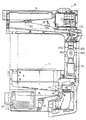
次に、パチンコ遊技機1の裏面の構造について図2を参照して説明する。
可変表示装置8の背面では、図2に示すように、機構板36の上部に球貯留タンク38が設けられ、パチンコ遊技機1が遊技機設置島に設置された状態でその上方から遊技球が球貯留タンク38に供給される。球貯留タンク38内の遊技球は、誘導樋39を通って球払出装置に至る。
Next, the structure of the back surface of the
On the back surface of the
機構板36には、中継基板30を介して可変表示部9を制御する可変表示制御ユニット29、基板ケース32に覆われ遊技制御用マイクロコンピュータ等が搭載された遊技制御基板(主基板)31、可変表示制御ユニット29と遊技制御基板31との間の信号を中継するための中継基板33、および遊技球の払出制御を行う払出制御用マイクロコンピュータ等が搭載された払出制御基板37が設置されている。さらに、機構板36の下部には、モータの回転力を利用して打球を遊技領域7に発射する打球発射装置34と、遊技効果ランプ・LED28a,28b,28c、賞球ランプ51および球切れランプ52に信号を送るためのランプ制御基板35が設置されている。
The
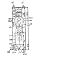
また、図3はパチンコ遊技機1の機構板を背面からみた背面図である。球貯留タンク38に貯留された玉は誘導樋39を通り、図3に示されるように、球切れ検出器(球切れスイッチ)187a,187bを通過して球供給樋186a,186bを経て球払出装置97に至る。球払出装置97から払い出された遊技球は、連絡口45を通ってパチンコ遊技機1の前面に設けられている打球供給皿3に供給される。連絡口45の側方には、パチンコ遊技機1の前面に設けられている余剰玉受皿4に連通する余剰玉通路46が形成されている。入賞にもとづく景品球が多数払い出されて打球供給皿3が満杯になり、ついには遊技球が連絡口45に到達した後さらに遊技球が払い出されると遊技球は、余剰玉通路46を経て余剰玉受皿4に導かれる。さらに遊技球が払い出されると、感知レバー47が満タンスイッチ48を押圧して満タンスイッチ48がオンする。その状態では、球払出装置97内のステッピングモータの回転が停止して球払出装置97の動作が停止するとともに打球発射装置34の駆動も停止する。
FIG. 3 is a rear view of the mechanism plate of the
賞球払出制御を行うために、入賞口スイッチ(図示せず)、始動口スイッチ17およびVカウントスイッチ22からの信号が、主基板31に送られる。主基板31のCPU56は、始動口スイッチ17がオンすると6個の賞球払出に対応した入賞が発生したことを知る。また、カウントスイッチ23がオンすると15個の賞球払出に対応した入賞が発生したことを知る。そして、入賞口スイッチがオンすると10個の賞球払出に対応した入賞が発生したことを知る。なお、この実施の形態では、例えば、入賞口24に入賞した遊技球は、入賞口24からの入賞球流路に設けられている入賞口スイッチ24aで検出され、入賞口19に入賞した遊技球は、入賞口19からの入賞球流路に設けられている入賞口スイッチ19aで検出される。
In order to perform prize ball payout control, signals from a winning opening switch (not shown), the
次に、機構板36に設置されている中間ベースユニットの構成について説明する。中間ベースユニットには、球供給樋186a,186bや球払出装置97が設置される。図4に示すように、中間ベースユニットの上下には連結凹突部182が形成されている。連結凹突部182は、中間ベースユニットと機構板36の上部ベースユニットおよび下部ベースユニットを連結固定するものである。
Next, the configuration of the intermediate base unit installed on the
中間ベースユニットの上部には通路体184が固定されている。そして、通路体184の下部に球払出装置97が固定されている。通路体184は、カーブ樋174(図3参照)によって流下方向を左右方向に変換された2列の遊技球を流下させる払出球通路186a,186bを有する。払出球通路186a,186bの上流側には、球切れスイッチ187a,187bが設置されている。球切れスイッチ187a,187bは、払出球通路186a,186b内の遊技球の有無を検出するものであって、球切れスイッチ187a,187bが遊技球を検出しなくなると球払出装置97における払出モータ(図4において図示せず)の回転を停止して球払出が不動化される。
A
なお、球切れスイッチ187a,187bは、払出球通路186a,186bに27〜28個程度の遊技球が存在することを検出できるような位置に係止片188によって係止されている。
The ball break switches 187a and 187b are locked by locking
通路体184の中央部は、内部を流下する遊技球の玉圧を弱めるように、左右に湾曲する形状に形成されている。そして、払出球通路186a,186bの間に止め穴189が形成されている。止め穴189の裏面は中間ベースユニットに設けられている取付ボスがはめ込まれる。その状態で止めねじがねじ止めされて、通路体184は中間ベースユニットに固定される。なお、ねじ止めされる前に、中間ベースユニットに設けられている係止突片185によって通路体184の位置合わせを行えるようになっている。
The central portion of the
通路体184の下方には、球払出装置97に遊技球を供給するとともに故障時等には球払出装置97への遊技球の供給を停止する球止め装置190が設けられている。球止め装置190の下方に設置される球払出装置97は、直方体状のケース198の内部に収納されている。ケース198の左右4箇所には突部が設けられている。各突部が中間ベースユニットに設けられている位置決め突片に係った状態で、中間ベースユニットの下部に設けられている弾性係合片にケース198の下端がはめ込まれる。
Below the
図5は球払出装置97の分解斜視図である。球払出装置97の構成および作用を図5を参照して説明する。この実施形態における球払出装置97は、ステッピングモータ(払出モータ)289がスクリュー288を回転させることによりパチンコ玉を1個ずつ払い出す。なお、球払出装置97は、入賞にもとづく景品球だけでなく、貸し出すべき遊技球も払い出す。
FIG. 5 is an exploded perspective view of the
図5に示すように、球払出装置97は、2つのケース198a,198bを有する。それぞれのケース198a,198bの左右2箇所に、球払出装置97の設置位置上部に設けられた位置決め突片に当接される係合突部280が設けられている。また、それぞれのケース198a,198bには、球供給路281a,281bが形成されている。球供給路281a,281bは湾曲面282a,282bを有し、湾曲面282a,282bの終端の下方には、球送り水平路284a,284bが形成されている。さらに、球送り水平路284a,284bの終端に球排出路283a,283bが形成されている。
As shown in FIG. 5, the
球供給路281a,281b、球送り水平路284a,284b、球排出路283a,283bは、ケース198a,198bをそれぞれ前後に区画する区画壁295a,295bの前方に形成されている。また、区画壁295a,295bの前方において、玉圧緩衝部材285がケース198a,198b間に挟み込まれる。玉圧緩衝部材285は、球払出装置97に供給される玉を左右側方に振り分けて球供給路281a,281bに誘導する。
The
また、玉圧緩衝部材285の下部には、発光素子(LED)286と受光素子(図示せず)とによる払出モータ位置センサが設けられている。発光素子286と受光素子とは、所定の間隔をあけて設けられている。そして、この間隔内に、スクリュー288の先端が挿入されるようになっている。なお、玉圧緩衝部材285は、ケース198a,198bが張り合わされたときに、完全にその内部に収納固定される。
In addition, below the ball
球送り水平路284a,284bには、払出モータ289によって回転させられるスクリュー288が配置されている。払出モータ289はモータ固定板290に固定され、モータ固定板290は、区画壁295a,295bの後方に形成される固定溝291a,291bにはめ込まれる。その状態で払出モータ289のモータ軸が区画壁295a,295bの前方に突出するので、その突出の前方にスクリュー288が固定される。スクリュー288の外周には、払出モータ289の回転によって球送り水平路284a,284bに載置された遊技球を前方に移動させるための螺旋突起288aが設けられている。
そして、スクリュー288の先端には、発光素子286を収納するように凹部が形成され、その凹部の外周には、2つの切欠部292が互いに180度離れて形成されている。従って、スクリュー288が1回転する間に、発光素子286からの光は、切欠部292を介して受光素子で2回検出される。
A recess is formed at the tip of the
つまり、発光素子286と受光素子とによる払出モータ位置センサは、スクリュー288を定位置で停止するためのものであり、かつ、払出動作が行われた旨を検出するものである。なお、発光素子286、受光素子および払出モータ289からの配線は、まとめられてケース198a,198bの後部下方に形成された引出穴から外部に引き出されコネクタに結線される。
In other words, the payout motor position sensor including the
遊技球が球送り水平路284a,284bに載置された状態において、払出モータ289が回転すると、スクリュー288の螺旋突起288aによって、遊技球は、球送り水平路284a,284b上を前方に向かって移動する。そして、遂には、球送り水平路284a,284bの終端から球排出路283a,283bに落下する。このとき、左右の球送り水平路284a,284bからの落下は交互に行われる。すなわち、スクリュー288が半回転する毎に一方から1個の遊技球が落下する。従って、1個の遊技球が落下する毎に、発光素子286からの光が受光素子によって検出される。
When the
図4に示すように、球払出装置97の下方には、球振分部材311が設けられている。球振分部材311は、振分用ソレノイド310によって駆動される。例えば、ソレノイド310のオン時には、球振分部材311は右側に倒れ、オフ時には左側に倒れる。振分用ソレノイド310の下方には、近接スイッチによる賞球カウントスイッチ301Aおよび球貸しカウントスイッチ301Bが設けられている。入賞にもとづく賞球時には、球振分部材311は右側に倒れ、球排出路283a,283bからの玉はともに賞球カウントスイッチ301Aを通過する。また、球貸し時には、球振分部材311は左側に倒れ、球排出路283a,283bからの玉はともに球貸しカウントスイッチ301Bを通過する。従って、球払出装置97は、賞球時と球貸し時とで払出流下路を切り替えて、所定数の遊技媒体の払出を行うことができる。
As shown in FIG. 4, a
このように、球振分部材311を設けることによって、2条の玉流路を落下してきた玉は、賞球カウントスイッチ301Aと球貸しカウントスイッチ301Bとのうちのいずれか一方しか通過しない。従って、賞球であるのか球貸しであるのかの判断をすることなく、賞球カウントスイッチ301Aと球貸しカウントスイッチ301Bの検出出力から、直ちに賞球数または球貸し数を把握することができる。
In this way, by providing the
図6は、主基板31における回路構成の一例を示すブロック図である。なお、図6には、払出制御基板37、ランプ制御基板35、音声制御基板70、発射制御基板91および表示制御基板80も示されている。主基板31には、プログラムに従ってパチンコ遊技機1を制御する基本回路53と、ゲートスイッチ12、始動口スイッチ17、Vカウントスイッチ22、カウントスイッチ23入賞口スイッチ19a,24a、満タンスイッチ48および賞球カウントスイッチ301Aからの信号を基本回路53に与えるスイッチ回路58と、可変入賞球装置15を開閉するソレノイド16および開閉板20を開閉するソレノイド21を基本回路53からの指令に従って駆動するソレノイド回路59と、始動記憶表示器18の点灯および滅灯を行うとともに7セグメントLEDによる可変表示器10と装飾ランプ25とを駆動するランプ・LED回路60とが搭載されている。
FIG. 6 is a block diagram illustrating an example of a circuit configuration in the
また、基本回路53から与えられるデータに従って、大当りの発生を示す大当り情報、可変表示部9の画像表示開始に利用された始動入賞球の個数を示す始動情報、確率変動が生じたことを示す確変情報等をホール管理コンピュータ等のホストコンピュータに対して出力する情報出力回路64を含む。
Further, according to the data given from the
基本回路53は、ゲーム制御用のプログラム等を記憶するROM54、ワークメモリとして使用される記憶手段の一例であるRAM55、制御用のプログラムに従って制御動作を行うCPU56およびI/Oポート部57を含む。この実施の形態では、ROM54,RAM55はCPU56に内蔵されている。すなわち、CPU56は、1チップマイクロコンピュータである。なお、1チップマイクロコンピュータは、少なくともRAM55が内蔵されていればよく、ROM54およびI/Oポート部57は外付けであっても内蔵されていてもよい。また、I/Oポート部57は、マイクロコンピュータにおける情報入出力可能な端子である。
The
さらに、主基板31には、電源投入時に基本回路53をリセットするための初期リセット回路65と、基本回路53から与えられるアドレス信号をデコードしてI/Oポート部57のうちのいずれかのI/Oポートを選択するための信号を出力するアドレスデコード回路67とが設けられている。
なお、球払出装置97から主基板31に入力されるスイッチ情報もあるが、図4ではそれらは省略されている。
Further, the
In addition, there is switch information input to the
遊技球を打撃して発射する打球発射装置は発射制御基板91上の回路によって制御される駆動モータ94で駆動される。そして、駆動モータ94の駆動力は、操作ノブ5の操作量に従って調整される。すなわち、発射制御基板91上の回路によって、操作ノブ5の操作量に応じた速度で打球が発射されるように制御される。
A ball hitting device for hitting and launching a game ball is driven by a
なお、この実施の形態では、主基板31のCPU56が可変表示器(普通図柄表示器)18の表示制御を行うが、普通図柄表示器も、表示制御基板80に搭載されている表示制御手段によって制御されるように構成してもよい。また、ランプ制御基板35に搭載されているランプ制御手段が、遊技領域内のランプ・LEDも制御するように構成してもよい。
In this embodiment, the
図7は、払出制御基板37および球払出装置97の構成要素などの賞球に関連する構成要素を示すブロック図である。図7に示すように、満タンスイッチ48からの検出信号は、中継基板71を介して主基板31のI/Oポート57に入力される。満タンスイッチ48は、余剰玉受皿4の満タンを検出するスイッチである。
FIG. 7 is a block diagram showing components related to a prize ball, such as components of the
球切れスイッチ187(187a,187b)からの検出信号は、中継基板72および中継基板71を介して主基板31のI/Oポート57に入力される。球切れ検出スイッチ167は球貯留タンク38内の補給玉の不足を検出するスイッチであり、球切れスイッチ187は、払出球通路内の遊技球の有無を検出するスイッチである。
A detection signal from the ball break switch 187 (187a, 187b) is input to the I / O port 57 of the
入賞があると、払出制御基板37には、主基板31から賞球個数を示す賞球制御コマンドが入力される。賞球個数を示す賞球制御コマンドは、入力バッファ回路373を介してI/Oポート372aに入力される。入力バッファ回路373における各バッファは、主基板31から払出制御基板37へ向かう方向にのみ信号を通過させることができる。従って、払出制御基板37側から主基板31側に信号が伝わる余地はない。払出制御基板37内の回路に不正改造が加えられても、不正改造によって出力される信号が主基板31側に伝わることはない。また、主基板31において、賞球制御コマンドを出力する出力ポート577,578の外側にバッファ回路68(不可逆性送信手段)が設けられている。このような構成によれば、外部から主基板31の内部に入力される信号が阻止されるので、払出制御基板37から主基板31に信号が与えられる可能性がある信号ラインをより確実になくすことができる。
When there is a win, a prize ball control command indicating the number of prize balls is input from the
主基板31のCPU56は、球切れスイッチ187からの検出信号が球切れ状態を示しているか、または、満タンスイッチ48からの検出信号が満タン状態を示していると、球払出禁止を指示する賞球制御コマンドを送出する。球払出禁止を指示する賞球制御コマンドを受信すると、払出制御基板37の払出制御用CPU371は、球払出処理を停止する。
The
さらに、賞球カウントスイッチ301Aおよび球貸しカウントスイッチ301Bからの検出信号も、中継基板72および中継基板71を介して主基板31のI/Oポート57に入力される。また、賞球カウントスイッチ301Aおよび球貸しカウントスイッチ301Bは、球払出装置97の賞球機構部分に設けられ、実際に払い出された賞球を検出する。
Further, detection signals from the prize
入賞があると、払出制御基板37には、主基板31の出力ポート(ポートG,H)577,578から賞球個数を示す賞球制御コマンドが入力される。出力ポート577は8ビットのデータを出力し、出力ポート578は1ビットのストローブ信号(INT信号)を出力する。賞球個数を示す賞球制御コマンドは、入力バッファ回路373を介してI/Oポート372aに入力される。払出制御用CPU371は、I/Oポート372aを介して賞球制御コマンドを入力し、賞球制御コマンドに応じて球払出装置97を駆動して賞球払出を行う。なお、この実施の形態では、払出制御用CPU371は、1チップマイクロコンピュータであり、少なくともRAMが内蔵されている。
When there is a prize, a prize ball control command indicating the number of prize balls is input to the
払出制御用CPU371は、出力ポート372gを介して、貸し玉数を示す球貸し個数信号をターミナル基板160に出力し、ブザー駆動信号をブザー基板75に出力する。ブザー基板75にはブザーが搭載されている。さらに、出力ポート372eを介して、エラー表示用LED374にエラー信号を出力する。
The payout control CPU 371 outputs a ball lending number signal indicating the number of lending balls to the
さらに、払出制御基板37の入力ポート372bには、中継基板72を介して、賞球カウントスイッチ301Aの検出信号の検出信号が入力される。払出制御基板37からの払出モータ289への駆動信号は、出力ポート372cおよび中継基板72を介して球払出装置97の賞球機構部分における払出モータ289に伝えられる。また、払出制御基板37から振分用ソレノイド310への駆動信号は、出力ポート372dおよび中継基板72を介して球払出装置97の振分用ソレノイド310に伝えられる。
Further, the detection signal of the detection signal of the prize ball count switch 301 </ b> A is input to the
カードユニット50には、カードユニット制御用マイクロコンピュータが搭載されている。また、カードユニット50には、端数表示スイッチ152、連結台方向表示器153、カード投入表示ランプ154およびカード挿入口155が設けられている(図1参照)。残高表示基板74には、打球供給皿3の近傍に設けられている度数表示LED、球貸しスイッチおよび返却スイッチが接続される。
The card unit 50 is equipped with a card unit control microcomputer. Further, the card unit 50 is provided with a
残高表示基板74からカードユニット50には、遊技者の操作に応じて、球貸しスイッチ信号および返却スイッチ信号が払出制御基板37を介して与えられる。また、カードユニット50から残高表示基板74には、プリペイドカードの残高を示すカード残高表示信号および球貸し可表示信号が払出制御基板37を介して与えられる。カードユニット50と払出制御基板37の間では、ユニット操作信号(BRDY信号)、球貸し要求信号(BRQ信号)、球貸し完了信号(EXS信号)およびパチンコ機動作信号(PRDY信号)がI/Oポート372fを介してやりとりされる。
A ball lending switch signal and a return switch signal are given from the balance display board 74 to the card unit 50 via the
パチンコ遊技機1の電源が投入されると、払出制御基板37の払出制御用CPU371は、カードユニット50にPRDY信号を出力する。カードユニット50においてカードが受け付けられ、球貸しスイッチが操作され球貸しスイッチ信号が入力されると、カードユニット制御用マイクロコンピュータは、払出制御基板37にBRDY信号を出力する。この時点から所定の遅延時間が経過すると、カードユニット制御用マイクロコンピュータは、払出制御基板37にBRQ信号を出力する。そして、払出制御基板37の払出制御用CPU371は、BRQ信号に応じてえXS信号をオンするとともに、払出モータ289を駆動し、所定個の貸し玉を遊技者に払い出す。そして、払出が完了したら、払出制御用CPU371は、カードユニット50にEXS信号をオフ状態にする。
When the power of the
以上のように、カードユニット50からの信号は全て払出制御基板37に入力される構成になっている。従って、球貸し制御に関して、カードユニット50から主基板31に信号が入力されることはなく、主基板31の基本回路53にカードユニット50の側から不正に信号が入力される余地はない。なお、主基板31および払出制御基板37には、ソレノイドおよびモータやランプを駆動するためのドライバ回路が搭載されているが、図7では、それらの回路は省略されている。
As described above, all signals from the card unit 50 are input to the
この実施の形態では、主基板31および払出制御基板37におけるRAMは、バックアップ電源でバックアップされている。すなわち、遊技機に対する電力供給が停止しても、所定期間はRAMの内容が保存される。そして、各CPUは、電源電圧の低下を検出すると、所定の処理を行った後に電源復旧待ちの状態になる。また、電源投入時に、各CPUは、RAMにデータが保存されている場合には、保存データにもとづいて電源断前の状態を復元する。
In this embodiment, the RAM in the
図8は、電源監視および電源バックアップのためのCPU56周りの一構成例を示すブロック図である。図8に示すように、第1の電源監視回路(第1の電源監視手段)からの電圧低下信号が、CPU56のマスク不能割込端子(NMI端子)に接続されている。第1の電源監視回路は、遊技機が使用する各種直流電源のうちのいずれかの電源の電圧を監視して電源電圧低下を検出する回路である。この実施の形態では、VSLの電源電圧を監視して電圧値が所定値以下になるとローレベルの電圧低下信号を発生する。VSLは、遊技機で使用される直流電圧のうちで最大のものであり、この例では+30Vである。従って、CPU56は、割込処理によって電源断の発生を確認することができる。なお、この実施の形態では、第1の電源監視回路は、後述する電源基板に搭載されている。
FIG. 8 is a block diagram showing an example of the configuration around the
図8には、初期リセット回路65も示されているが、この実施の形態では、初期リセット回路65は、第2の電源監視回路(第2の電源監視手段)も兼ねている。すなわち、リセットIC651は、電源投入時に、外付けのコンデンサに容量で決まる所定時間だけ出力をローレベルとし、所定時間が経過すると出力をハイレベルにする。すなわち、リセット信号をハイレベルに立ち上げてCPU56を動作可能状態にする。また、リセットIC651は、第1の電源監視回路が監視する電源電圧と等しい電源電圧であるVSLの電源電圧を監視して電圧値が所定値(第1の電源監視回路が電圧低下信号を出力する電源電圧値よりも低い値)以下になるとローレベルの電圧低下信号を発生する。従って、CPU56は、第1の電源監視回路からの電圧低下信号に応じて所定の電力供給停止時処理を行った後、システムリセットされる。なお、この実施の形態では、リセット信号と第2の電源監視回路からの電圧低下信号とは同一の信号である。
Although the initial reset circuit 65 is also shown in FIG. 8, in this embodiment, the initial reset circuit 65 also serves as a second power supply monitoring circuit (second power supply monitoring means). That is, when the power is turned on, the
図8に示すように、リセットIC651からのリセット信号は、NAND回路947に入力されるとともに、反転回路(NOT回路)944を介してカウンタIC941のクリア端子に入力される。カウンタIC941は、クリア端子への入力がローレベルになると、発振器943からのクロック信号をカウントする。そして、カウンタIC941のQ5出力がNOT回路945,946を介してNAND回路947に入力される。また、カウンタIC941のQ6出力は、フリップフロップ(FF)942のクロック端子に入力される。フリップフロップ942のD入力はハイレベルに固定され、Q出力は論理和回路(OR回路)949に入力される。OR回路949の他方の入力には、NAND回路947の出力がNOT回路948を介して導入される。そして、OR回路949の出力がCPU56のリセット端子に接続されている。このような構成によれば、電源投入時に、CPU56のリセット端子に2回のリセット信号(ローレベル信号)が与えられるので、CPU56は、確実に動作を開始する。
As shown in FIG. 8, the reset signal from the
そして、例えば、第1の電源監視回路の検出電圧(電圧低下信号を出力することになる電圧)を+22Vとし、第2の電源監視回路の検出電圧を+9Vとする。そのように構成した場合には、第1の電源監視回路と第2の電源監視回路とは、同一の電源VSLの電圧を監視するので、第1の電圧監視回路が電圧低下信号を出力するタイミングと第2の電圧監視回路が電圧低下信号を出力するタイミングの差を所望の所定期間に確実に設定することができる。所望の所定期間とは、第1の電源監視回路からの電圧低下信号に応じて電力供給停止時処理を開始してから電力供給停止時処理が確実に完了するまでの期間である。 For example, the detection voltage of the first power supply monitoring circuit (voltage that outputs a voltage drop signal) is + 22V, and the detection voltage of the second power supply monitoring circuit is + 9V. In such a configuration, since the first power monitoring circuit and the second power monitoring circuit monitor the voltage of the same power supply VSL, the timing when the first voltage monitoring circuit outputs the voltage drop signal. And the timing at which the second voltage monitoring circuit outputs the voltage drop signal can be reliably set to a desired predetermined period. The desired predetermined period is a period from when the power supply stop process is started in response to the voltage drop signal from the first power supply monitoring circuit until the power supply stop process is reliably completed.
この例では、第1の電源監視手段が検出信号を出力することになる第1検出条件は+30V電源電圧が+22Vにまで低下したことであり、第2の電源監視手段が検出信号を出力することになる第2検出条件は+30V電源電圧が+9Vにまで低下したことになる。ただし、ここで用いられている電圧値は一例であって、他の値を用いてもよい。 In this example, the first detection condition for the first power supply monitoring means to output the detection signal is that the + 30V power supply voltage has dropped to + 22V, and the second power supply monitoring means outputs the detection signal. The second detection condition that becomes is that the + 30V power supply voltage is lowered to + 9V. However, the voltage value used here is an example, and other values may be used.
ただし、監視範囲が狭まるが、第1の電圧監視回路および第2の電圧監視回路の監視電圧として+5V電源電圧を用いることも可能である。その場合にも、第1の電圧監視回路の検出電圧は、第2の電圧監視回路の検出電圧よりも高く設定される。 However, although the monitoring range is narrowed, it is also possible to use a + 5V power supply voltage as the monitoring voltage of the first voltage monitoring circuit and the second voltage monitoring circuit. Also in that case, the detection voltage of the first voltage monitoring circuit is set higher than the detection voltage of the second voltage monitoring circuit.
CPU56等の駆動電源である+5V電源から電力が供給されていない間、RAMの少なくとも一部は、電源基板から供給されるバックアップ電源によってバックアップされ、遊技機に対する電源が断しても内容は保存される。そして、+5V電源が復旧すると、初期リセット回路65からリセット信号が発せられるので、CPU56は、通常の動作状態に復帰する。そのとき、必要なデータがバックアップされているので、停電等からの復旧時には停電発生時の遊技状態に復帰することができる。
While power is not supplied from the + 5V power source that is the driving power source of the
なお、図8では、電源投入時にCPU56のリセット端子に2回のリセット信号(ローレベル信号)が与えられる構成が示されたが、リセット信号の立ち上がりタイミングが1回しかなくても確実にリセット解除されるCPUを使用する場合には、符号941〜949で示された回路素子は不要である。その場合、リセットIC651の出力がそのままCPU56のリセット端子に接続される。
Although FIG. 8 shows a configuration in which a reset signal (low level signal) is given to the reset terminal of the
図9は、遊技機の電源基板910の一構成例を示すブロック図である。電源基板910は、主基板31、表示制御基板80、音声制御基板70、ランプ制御基板35および払出制御基板37等の電気部品制御基板と独立して設置され、遊技機内の各電気部品制御基板および機構部品が使用する電圧を生成する。この例では、AC24V、VSL(DC+30V)、DC+21V、DC+12VおよびDC+5Vを生成する。また、バックアップ電源となるコンデンサ916は、DC+5Vすなわち各基板上のIC等を駆動する電源のラインから充電される。
FIG. 9 is a block diagram illustrating a configuration example of the
トランス911は、交流電源からの交流電圧を24Vに変換する。AC24V電圧は、コネクタ915に出力される。また、整流回路912は、AC24Vから+30Vの直流電圧を生成し、DC−DCコンバータ913およびコネクタ915に出力する。DC−DCコンバータ913は、+22V、+12Vおよび+5Vを生成してコネクタ915に出力する。コネクタ915は例えば中継基板に接続され、中継基板から各電気部品制御基板および機構部品に必要な電圧の電力が供給される。なお、トランス911の入力側には、遊技機に対する電源供給を停止したり開始させたりするための電源スイッチ918が設置されている。
The transformer 911 converts AC voltage from the AC power source into 24V. The AC 24V voltage is output to the connector 915. The rectifier circuit 912 also generates a DC voltage of +30 V from AC 24 V and outputs it to the DC-DC converter 913 and the connector 915. The DC-DC converter 913 generates + 22V, + 12V, and + 5V and outputs them to the connector 915. The connector 915 is connected to, for example, a relay board, and power of a voltage necessary for each electric component control board and the mechanism component is supplied from the relay board. Note that a
DC−DCコンバータ913からの+5Vラインは分岐してバックアップ+5Vラインを形成する。バックアップ+5Vラインとグラウンドレベルとの間には大容量のコンデンサ916が接続されている。コンデンサ916は、遊技機に対する電力供給が遮断されたときの電気部品制御基板のバックアップRAM(電源バックアップされているRAMすなわち記憶内容保持状態となりうる記憶手段)に対して記憶状態を保持できるように電力を供給するバックアップ電源となる。また、+5Vラインとバックアップ+5Vラインとの間に、逆流防止用のダイオード917が挿入される。
The + 5V line from the DC-DC converter 913 branches to form a backup + 5V line. A large-
なお、バックアップ電源として、+5V電源から充電可能な電池を用いてもよい。電池を用いる場合には、+5V電源から電力供給されない状態が所定時間継続すると容量がなくなるような充電池が用いられる。 A battery that can be charged from a + 5V power supply may be used as the backup power supply. In the case of using a battery, a rechargeable battery is used in which the capacity disappears when a state in which no power is supplied from the +5 V power source continues for a predetermined time.
また、電源基板910には、上述した第1の電源監視回路を構成する電源監視用IC902が搭載されている。電源監視用IC902は、VSL電源電圧を導入し、VSL電源電圧を監視することによって電源断の発生を検出する。具体的には、VSL電源電圧が所定値(この例では+22V)以下になったら、電源断が生ずるとして電圧低下信号を出力する。なお、監視対象の電源電圧は、各電気部品制御基板に搭載されている回路素子の電源電圧(この例では+5V)よりも高い電圧であることが好ましい。この例では、交流から直流に変換された直後の電圧であるVSLが用いられている。電源監視用IC902からの電圧低下信号は、主基板31や払出制御基板37等に供給される。
The
電源監視用IC902が電源断を検知するための所定値は、通常時の電圧より低いが、各電気部品制御基板上のCPUが暫くの間動作しうる程度の電圧である。また、電源監視用IC902が、CPU等の回路素子を駆動するための電圧(この例では+5V)よりも高く、また、交流から直流に変換された直後の電圧を監視するように構成されているので、CPUが必要とする電圧に対して監視範囲を広げることができる。従って、より精密な監視を行うことができる。さらに、監視電圧としてVSL(+30V)を用いる場合には、遊技機の各種スイッチに供給される電圧が+12Vであることから、電源瞬断時のスイッチオン誤検出の防止も期待できる。すなわち、+30V電源の電圧を監視すると、+30V作成の以降に作られる+12Vが落ち始める以前の段階でそれの低下を検出できる。よって、+12V電源の電圧が低下するとスイッチ出力がオン状態を呈するようになるが、+12Vより早く低下する+30V電源電圧を監視して電源断を認識すれば、スイッチ出力がオン状態を呈する前に電源復旧待ちの状態に入ってスイッチ出力を検出しない状態となることができる。
The predetermined value for the
また、電源監視用IC902は、電気部品制御基板とは別個の電源基板910に搭載されているので、第1の電源監視回路から複数の電気部品制御基板に電圧低下信号を供給することができる。電圧低下信号を必要とする電気部品制御基板が幾つあっても第1の電源監視手段は1つ設けられていればよいので、各電気部品制御基板における各電気部品制御手段が後述する復帰制御を行っても、遊技機のコストはさほど上昇しない。
Further, since the
なお、図9に示された構成では、電源監視用IC902の検出出力(電圧低下信号)は、バッファ回路918,919を介してそれぞれの電気部品制御基板(例えば主基板31と払出制御基板37)に伝達されるが、例えば、1つの検出出力を中継基板に伝達し、中継基板から各電気部品制御基板に同じ信号を分配する構成でもよい。また、電圧低下信号を必要とする基板数に応じたバッファ回路を設けてもよい。
In the configuration shown in FIG. 9, the detection output (voltage drop signal) of the power
次に遊技機の動作について説明する。
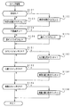
図10は、主基板31におけるCPU56が実行するメイン処理を示すフローチャートである。遊技機に対する電源が投入されると、メイン処理において、CPU56は、まず、停電からの復旧時であったか否か確認する(ステップS1)。停電からの復旧時であったか否かは、例えば、電源断時にバックアップRAM領域に設定される電源断フラグによって確認される。
Next, the operation of the gaming machine will be described.
FIG. 10 is a flowchart showing main processing executed by the
停電からの復旧時であった場合には、バックアップRAM領域のデータチェック(この例ではパリティチェック)を行う(ステップS3)。不測の電源断が生じた後に復旧した場合には、バックアップRAM領域のデータは保存されていたはずであるから、チェック結果は正常になる。チェック結果が正常でない場合には、内部状態を電源断時の状態に戻すことができないので、停電復旧時でない電源投入時に実行される初期化処理を実行する(ステップS4,S2)。 If it is time to recover from a power failure, a data check (parity check in this example) of the backup RAM area is performed (step S3). In the case of recovery after an unexpected power failure, the data in the backup RAM area should have been saved, so the check result is normal. If the check result is not normal, the internal state cannot be returned to the state when the power is cut off, and therefore an initialization process that is executed when the power is turned on not when the power failure is restored is executed (steps S4 and S2).
チェック結果が正常であれば、CPU56は、内部状態を電源断時の状態に戻すための遊技状態復旧処理を行うとともに(ステップS5)、電源断フラグをクリアする(ステップS6)。
If the check result is normal, the
停電からの復旧時でない場合には、CPU56は、通常の初期化処理を実行する(ステップS1,S2)。その後、メイン処理では、タイマ割込フラグの監視(ステップS6)の確認が行われるループ処理に移行する。なお、ループ内では、表示用乱数更新処理(ステップS7)も実行される。
If it is not time to recover from a power failure, the
なお、ここでは、ステップS1で停電からの復旧か否かを確認し、停電からの復旧時であればパリティチェックを行ったが、最初に、パリティチェックを実行し、チェック結果が正常でなければ停電からの復旧ではないと判断してステップS2の初期化処理を実行し、チェック結果が正常であれば遊技状態復帰処理を行ってもよい。すなわち、パリティチェックの結果をもって停電からの復旧であるか否かを判断してもよい。 Here, it is confirmed in step S1 whether or not the recovery from the power failure, and if the recovery from the power failure, the parity check is performed. First, the parity check is performed and the check result is not normal. If it is determined that the power is not recovered from the power failure, the initialization process of step S2 is executed. If the check result is normal, the game state return process may be performed. That is, it may be determined whether or not recovery from a power failure is made based on the result of the parity check.
また、停電復旧処理を実行するか否か判断する場合に、すなわち、遊技状態を復旧するか否か判断する際に、保存されていたRAMデータにおける特別プロセスフラグ等や始動入賞記憶数データによって、遊技機が遊技待機状態(図柄変動中でなく、大当り遊技中でなく、確変中でなく、また、始動入賞記憶がない状態)であることが確認されたら、遊技状態復旧処理を行わずに初期化処理を実行するようにしてもよい。 Further, when determining whether or not to execute the power failure recovery processing, that is, when determining whether or not to restore the gaming state, according to the special process flag or the like in the stored RAM data or the start winning memory number data, If it is confirmed that the gaming machine is in a game standby state (not changing in design, not in big hit game, not in probable change, and no start winning memory), it is initial without performing game state recovery processing. The process may be executed.
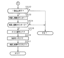
通常の初期化処理では、図11に示すように、レジスタおよびRAMのクリア処理(ステップS2a)と、必要な初期値設定処理(ステップS2b)が行われた後に、2ms毎に定期的にタイマ割込がかかるようにCPU56に設けられているタイマレジスタの初期設定(タイムアウトが2msであることと繰り返しタイマが動作する設定)が行われる(ステップS2c)。すなわち、ステップS2cで、タイマ割込を能動化する処理と、タイマ割込インタバルを設定する処理とが実行される。 In the normal initialization process, as shown in FIG. 11, after a register and RAM clear process (step S2a) and a necessary initial value setting process (step S2b) are performed, a timer allocation is periodically performed every 2 ms. Initial setting of the timer register provided in the CPU 56 (setting that the time-out is 2 ms and the timer repeatedly operates) is performed so as to cause a delay (step S2c). That is, in step S2c, processing for activating a timer interrupt and processing for setting a timer interrupt interval are executed.
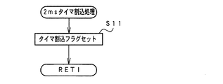
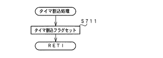
従って、この実施の形態では、CPU56の内部タイマが繰り返しタイマ割込を発生するように設定される。この実施の形態では、繰り返し周期は2msに設定される。そして、図12に示すように、タイマ割込が発生すると、CPU56は、タイマ割込フラグをセットする(ステップS11)。
Therefore, in this embodiment, the internal timer of the
CPU56は、ステップS8において、タイマ割込フラグがセットされたことを検出すると、タイマ割込フラグをリセットするとともに(ステップS9)、遊技制御処理を実行する(ステップS10)。以上の制御によって、この実施の形態では、遊技制御処理は2ms毎に起動されることになる。なお、この実施の形態では、タイマ割込処理ではフラグセットのみがなされ、遊技制御処理はメイン処理において実行されるが、タイマ割込処理で遊技制御処理を実行してもよい。
When detecting that the timer interrupt flag is set in step S8, the
図13は、ステップS10の遊技制御処理を示すフローチャートである。遊技制御処理において、CPU56は、まず、表示制御基板80に送出される表示制御コマンドをRAM55の所定の領域に設定する処理を行った後に(表示制御データ設定処理:ステップS21)、表示制御コマンドを出力する処理を行う(表示制御データ出力処理:ステップS22)。
FIG. 13 is a flowchart showing the game control process of step S10. In the game control process, the
次いで、各種出力データの格納領域の内容を各出力ポートに出力する処理を行う(データ出力処理:ステップS23)。また、ホール管理用コンピュータに出力される大当り情報、始動情報、確率変動情報などの出力データを格納領域に設定する出力データ設定処理を行う(ステップS24)。さらに、パチンコ遊技機1の内部に備えられている自己診断機能によって種々の異常診断処理が行われ、その結果に応じて必要ならば警報が発せられる(エラー処理:ステップS25)。
Next, a process of outputting the contents of the storage area for various output data to each output port is performed (data output process: step S23). Also, output data setting processing is performed for setting output data such as jackpot information, start information, probability variation information, etc., output to the hall management computer in the storage area (step S24). Further, various abnormality diagnosis processes are performed by the self-diagnosis function provided in the
次に、遊技制御に用いられる大当り判定用の乱数等の各判定用乱数を示す各カウンタを更新する処理を行う(ステップS26)。 Next, a process of updating each counter indicating each determination random number such as a big hit determination random number used for game control is performed (step S26).
さらに、CPU56は、特別図柄プロセス処理を行う(ステップS27)。特別図柄プロセス制御では、遊技状態に応じてパチンコ遊技機1を所定の順序で制御するための特別図柄プロセスフラグに従って該当する処理が選び出されて実行される。そして、特別図柄プロセスフラグの値は、遊技状態に応じて各処理中に更新される。また、普通図柄プロセス処理を行う(ステップS28)。普通図柄プロセス処理では、7セグメントLEDによる可変表示器10を所定の順序で制御するための普通図柄プロセスフラグに従って該当する処理が選び出されて実行される。そして、普通図柄プロセスフラグの値は、遊技状態に応じて各処理中に更新される。
Further, the
さらに、CPU56は、スイッチ回路58を介して、ゲートセンサ12、始動口センサ17、カウントセンサ23および入賞口スイッチ19a,24aの状態を入力し、各入賞口や入賞装置に対する入賞があったか否か判定する(スイッチ処理:ステップS29)。CPU56は、さらに、停止図柄の種類を決定する乱数等の表示用乱数を更新する処理を行う(ステップS30)。
Further, the
また、CPU56は、払出制御基板37との間の信号処理を行う(ステップS31)。すなわち、所定の条件が成立すると払出制御基板37に賞球制御コマンドを出力する。払出制御基板37に搭載されている払出制御用CPUは、賞球制御コマンドに応じて球払出装置97を駆動する。
Further, the
以上のように、メイン処理には遊技制御処理に移行すべきか否かを判定する処理が含まれ、CPU56の内部タイマが定期的に発生するタイマ割込にもとづくタイマ割込処理で遊技制御処理に移行すべきか否かを判定するためのフラグがセットされるので、遊技制御処理の全てが確実に実行される。つまり、遊技制御処理の全てが実行されるまでは、次回の遊技制御処理に移行すべきか否かの判定が行われないので、遊技制御処理中の全ての各処理が実行完了することは保証されている。
As described above, the main process includes a process for determining whether or not to shift to the game control process, and the timer control process based on the timer interrupt periodically generated by the internal timer of the
従来の一般的な遊技制御処理は、定期的に発生する外部割込によって、強制的に最初の状態に戻されていた。図13に示された例に則して説明すると、例えば、ステップS31の処理中であっても、強制的にステップS21の処理に戻されていた。つまり、遊技制御処理中の全ての各処理が実行完了する前に、次回の遊技制御処理が開始されてしまう可能性があった。 Conventional general game control processing is forcibly returned to the initial state by an external interrupt that occurs periodically. If it demonstrates in accordance with the example shown by FIG. 13, for example, even if it was during the process of step S31, it was forcibly returned to the process of step S21. In other words, there is a possibility that the next game control process will be started before all the processes in the game control process are completed.
なお、ここでは、主基板31のCPU56が実行する遊技制御処理は、CPU56の内部タイマが定期的に発生するタイマ割込にもとづくタイマ割込処理でセットされるフラグに応じて実行されたが、定期的に(例えば2ms毎)信号を発生するハードウェア回路を設け、その回路からの信号をCPU56の外部割込端子に導入し、割込信号によって遊技制御処理に移行すべきか否かを判定するためのフラグをセットするようにしてもよい。
Here, the game control process executed by the
そのように構成した場合にも、遊技制御処理の全てが実行されるまでは、フラグの判定が行われないので、遊技制御処理中の全ての各処理が実行完了することが保証される。 Even in such a configuration, the determination of the flag is not performed until all of the game control processes are executed, so that it is guaranteed that all the processes in the game control process are completed.
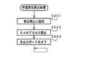
図14は、電源基板910の第1の電源監視回路からの電圧低下信号にもとづくNMIに応じて実行される停電発生NMI処理の一例を示すフローチャートである。停電発生NMI処理において、CPU56は、まず、割込禁止に設定する(ステップS41)。停電発生NMI処理ではRAM内容の保存を確実にするためにチェックサムの生成処理を行う。その処理中に他の割込処理が行われたのではチェックサムの生成処理が完了しないうちにCPUが動作し得ない電圧にまで低下してしまうことがことも考えられるので、まず、他の割込が生じないような設定がなされる。なお、停電発生NMI処理におけるステップS43〜S49は、電力供給停止時処理の一例である。
FIG. 14 is a flowchart showing an example of a power failure occurrence NMI process executed in response to the NMI based on the voltage drop signal from the first power supply monitoring circuit of the
なお、割込処理中では他の割込がかからないような仕様のCPUを用いている場合には、ステップS41の処理は不要である。 Note that the processing in step S41 is not necessary when a CPU having a specification that does not cause other interrupts during the interrupt processing is used.
次いで、CPU56は、電源断フラグが既にセットされているか否か確認する(ステップS42)。電源断フラグが既にセットされていれば、以後の処理を行わない。電源断フラグがセットされていなければ、以下の電力供給停止時処理を実行する。すなわち、ステップS43からステップS49の処理を実行する。
Next, the
まず、各レジスタの内容をバックアップRAM領域に格納する(ステップS43)。さらに、バックアップRAM領域のバックアップチェックデータ領域に適当な初期値を設定し(ステップS44)、初期値およびバックアップRAM領域のデータについて順次排他的論理和をとって(ステップS45)、最終的な演算値をバックアップパリティデータ領域に設定する(ステップS46)。その後、電源断フラグをセットする(ステップS47)。また、RAMアクセス禁止状態にする(ステップS48)。電源電圧が低下していくときには、各種信号線のレベルが不安定になってRAM内容が化ける可能性があるが、このようにRAMアクセス禁止状態にしておけば、バックアップRAM内のデータが化けることはない。そして、全ての出力ポートをオフ状態にする(ステップS49)。 First, the contents of each register are stored in the backup RAM area (step S43). Further, an appropriate initial value is set in the backup check data area of the backup RAM area (step S44), the exclusive value is sequentially calculated for the initial value and the data in the backup RAM area (step S45), and the final calculation value is obtained. Is set in the backup parity data area (step S46). Thereafter, a power-off flag is set (step S47). Further, the RAM access is prohibited (step S48). When the power supply voltage is lowered, the level of various signal lines may become unstable and the contents of the RAM may be altered, but if the RAM access is prohibited in this manner, the data in the backup RAM will be altered. There is no. Then, all output ports are turned off (step S49).
次いで、CPU56は、ループ処理にはいる。すなわち、何らの処理もしない状態になる。従って、図8に示されたリセットIC651からのリセット信号によって外部から動作禁止状態にされる前に、内部的に動作停止状態になる。よって、電源断時に確実にCPU56は動作停止する。その結果、上述したRAMアクセス禁止の制御および動作停止制御によって、電源電圧が低下していくことに伴って生ずる可能性がある異常動作に起因するRAMの内容破壊等を確実に防止することができる。
Next, the
なお、この実施の形態では、停電発生NMI処理では最終部でプログラムをループ状態にしたが、ホールト(HALT)命令を発行するように構成してもよい。 In this embodiment, in the power failure occurrence NMI processing, the program is looped at the final part, but a halt (HALT) instruction may be issued.
また、RAMアクセス禁止にする前にセットされる電源断フラグは、上述したように、電源投入時において停電からの復旧か否かを判断する際に使用される。また、ステップS41からS49の処理は、第2の電源監視手段が電圧低下信号を発生する前に完了する。換言すれば、第2の電源監視手段が電圧低下信号を発生する前に完了するように、第1の電圧監視手段および第2の電圧監視手段の検出電圧の設定が行われている。 Further, as described above, the power-off flag that is set before the RAM access is prohibited is used when determining whether or not to recover from a power failure when the power is turned on. Further, the processing of steps S41 to S49 is completed before the second power supply monitoring unit generates the voltage drop signal. In other words, the detection voltages of the first voltage monitoring means and the second voltage monitoring means are set so that the second power supply monitoring means is completed before generating the voltage drop signal.
この実施の形態では、電力供給停止時処理開始時に、電源断フラグの確認が行われる。そして、電源断フラグが既にセットされている場合には電力供給停止時処理を実行しない。上述したように、電源断フラグは、電力供給停止時処理が完了したことを示すフラグである。従って、例えば、リセット待ちのループ状態で何らかの原因で再度NMIが発生したとしても、電力供給停止時処理が重複して実行されてしまうようなことはない。 In this embodiment, the power-off flag is confirmed at the start of the power supply stop process. When the power-off flag is already set, the power supply stop process is not executed. As described above, the power-off flag is a flag indicating that the power supply stop process has been completed. Therefore, for example, even if NMI occurs again for some reason in a loop waiting for reset, the power supply stop process is not repeatedly executed.
ただし、割込処理中では他の割込がかからないような仕様のCPUを用いている場合には、ステップS42の判断は不要である。 However, if a CPU with specifications that do not cause other interrupts during interrupt processing is used, the determination in step S42 is not necessary.
図15は、バックアップパリティデータ作成方法を説明するための説明図である。ただし、図15に示す例では、簡単のために、バックアップデータRAM領域のデータのサイズを3バイトとする。電源電圧低下にもとづく停電発生処理において、図15(A)に示すように、バックアップチェックデータ領域に、初期データ(この例では00H)が設定される。次に、「00H」と「F0H」の排他的論理和がとられ、その結果と「16H」の排他的論理和がとられる。さらに、その結果と「DFH」の排他的論理和がとられる。そして、その結果(この例では「39H」)がバックアップパリティデータ領域に設定される。 FIG. 15 is an explanatory diagram for explaining a backup parity data creation method. However, in the example shown in FIG. 15, the size of the data in the backup data RAM area is 3 bytes for simplicity. In the power failure generation process based on the power supply voltage drop, as shown in FIG. 15A, initial data (00H in this example) is set in the backup check data area. Next, an exclusive logical sum of “00H” and “F0H” is taken, and an exclusive logical sum of “16H” is obtained. Further, an exclusive OR of the result and “DFH” is taken. Then, the result (“39H” in this example) is set in the backup parity data area.
電源が再投入されたときには、停電復旧処理においてパリティ診断が行われるが、図15(B)はパリティ診断の例を示す説明図である。バックアップ領域の全データがそのまま保存されていれば、電源再投入時に、図15(A)に示すようなデータがバックアップ領域に設定されている。 When the power is turned on again, parity diagnosis is performed in the power failure recovery process. FIG. 15B is an explanatory diagram illustrating an example of parity diagnosis. If all the data in the backup area is stored as it is, the data as shown in FIG. 15A is set in the backup area when the power is turned on again.
ステップS51の処理において、CPU56は、バックアップRAM領域のバックアップパリティデータ領域に設定されていたデータ(この例では「39H」)を初期データとして、バックアップデータ領域の各データについて順次排他的論理和をとる処理を行う。バックアップ領域の全データがそのまま保存されていれば、最終的な演算結果は、「00H」、すなわちバックアップチェックデータ領域に設定されているデータと一致する。バックアップRAM領域内のデータにビット誤りが生じていた場合には、最終的な演算結果は「00H」にならない。
In the processing of step S51, the
よって、CPU56は、最終的な演算結果とバックアップチェックデータ領域に設定されているデータとを比較して、一致すればパリティ診断正常とする。一致しなければ、パリティ診断異常とする。
Therefore, the
以上のように、この実施の形態では、遊技制御手段には、遊技機の電源が断しても、所定期間電源バックアップされる記憶手段(この例ではバックアップRAM)が設けられ、電源投入時に、CPU56(具体的にはCPU56が実行するプログラム)は、記憶手段がバックアップ状態にあればバックアップデータにもとづいて遊技状態を回復させる遊技状態復旧処理(ステップS5)を行うように構成される。 As described above, in this embodiment, the game control means is provided with a storage means (a backup RAM in this example) that is backed up for a predetermined period even when the power of the gaming machine is cut off. The CPU 56 (specifically, a program executed by the CPU 56) is configured to perform a game state recovery process (step S5) for recovering the game state based on the backup data if the storage means is in the backup state.
この実施の形態では、図9に示されたように電源基板910に第1の電源監視手段が搭載され、図8に示されたように主基板31に第2の電源監視手段が搭載されている。そして、電源電圧が低下していくときに、第2の電源監視手段(この例ではリセットIC651)が電圧低下信号(システムリセット信号)を発生する時期は、第1の電源監視手段(この例では電源監視用IC902)が電圧低下信号を発生する時期よりも後になるように設定されている。
In this embodiment, the first power supply monitoring means is mounted on the
すると、CPU56は、第1の電源監視手段(電源監視用IC902)からの電圧低下信号にもとづいて停電発生処理(電力供給停止時処理)を実行した後にループ状態に入るのであるが、ループ状態において、リセット状態に入ることになる。すなわち、CPU56の動作が完全に停止する。ループ状態においては+5V電源電圧値が徐々に低下するので入出力状態が不定になるが、CPU56はリセット状態になるので、不定データにもとづいて異常動作してしまうことは防止される。
Then, the
このように、この実施の形態では、CPU56が、第1の電源監視手段からの検出出力の入力に応じてループ状態に入るとともに、第2の電源監視手段からの検出出力の入力に応じてシステムリセットされるように構成したので、電源断時に確実なデータ保存を行うことができ、遊技者に不利益がもたらされることを防止することができる。
Thus, in this embodiment, the
なお、この実施の形態では、第1の電源監視回路と第2の電源監視回路とが、同一の電源電圧を監視しているが、異なる電源電圧を監視してもよい。例えば、電源基板910の第1の電源監視回路が+30V電源電圧を監視し、主基板31の第2の電源監視回路が+5V電源電圧を監視してもよい。そして、第2の電源監視回路がローレベルの電圧低下信号を発生するタイミングは第1の電源監視回路が電圧低下信号を発生するタイミングに対して遅くなるように、主基板31の第2の電源監視回路のしきい値レベル(電圧低下信号を発生する電圧レベル)が設定される。例えば、しきい値は4.25Vである。4.25Vは、通常時の電圧より低いが、CPU56が暫くの間動作しうる程度の電圧である。
In this embodiment, the first power supply monitoring circuit and the second power supply monitoring circuit monitor the same power supply voltage, but different power supply voltages may be monitored. For example, the first power supply monitoring circuit on the
また、上記の実施の形態では、CPU56は、マスク不能割込端子(NMI端子)を介して電源基板からの第1の電圧低下信号(第1の電源監視手段からの電圧低下信号)を検知したが、第1の電圧低下信号をマスク可能割込割込端子(IRQ端子)に導入してもよい。その場合には、割込処理(IRQ処理)で電力供給停止時処理が実行される。
In the above embodiment, the
図16は、図13に示された遊技制御処理におけるスイッチ処理(ステップS29)の賞球制御に関連する部分を示すフローチャートである。スイッチ処理において、CPU56は、球切れスイッチ187によって球切れを検出すると球切れフラグをセットする(ステップS121,S122)。また、球切れスイッチ187によって球切れでないことを検出すると球切れフラグをリセットする(ステップS121,S123)。
FIG. 16 is a flowchart showing a portion related to prize ball control in the switch process (step S29) in the game control process shown in FIG. In the switch process, the
次いで、満タンスイッチ48によって下皿満タンを検出すると満タンフラグをセットする(ステップS124,S125)。また、満タンスイッチ48によって下皿満タンでないことを検出すると満タンフラグをリセットする(ステップS124,S126)。
Next, when the lower pan full tank is detected by the
さらに、カウントスイッチ23がオンしたことを検出すると、大入賞口用カウンタを+1し(ステップS131,S132)、入賞口スイッチ19a,24aのいずれかがオンしたことを検出すると、普通入賞口用カウンタを+1し(ステップS133,S134)、始動口スイッチ17がオンしたことを検出すると始動入賞口用カウンタを+1する(ステップS135,S136)。
Further, when it is detected that the
なお、大入賞口用カウンタ、普通入賞口用カウンタおよび始動入賞口用カウンタは、それぞれの入賞口への入賞数を計数するためのカウンタである。 Note that the large winning opening counter, the normal winning opening counter, and the starting winning opening counter are counters for counting the number of winning combinations at each winning opening.
図17は、主基板31から払出制御基板37に送信される賞球制御コマンドのビット構成の一例を示す説明図である。図17に示すように、1バイト中の上位4ビットが制御指定部として使用され、下位4ビットが賞球数を示す領域として用いられる。
FIG. 17 is an explanatory diagram showing an example of a bit configuration of a prize ball control command transmitted from the
図18に示すように、制御指定部において、ビット7,6,5,4が「0,1,0,0」であれば払出個数指定コマンドであることを示し、「0,1,0,1」であれば払出指定コマンドであることを示す。払出個数指定コマンドは、主基板31のCPU56が入賞を検出すると直ちに払出制御基板37に送出される。
As shown in FIG. 18, if
ビット7,6,5,4が「1,0,0,0」である払出停止指定コマンドは、補給玉がなくなったことが検出されたとき、または余剰玉受皿4が満タンが検出されたときに主基板31から送信される。また、ビット7,6,5,4が「1,0,1,0」である払出停止解除指定コマンドは、補給球が存在し、かつ、余剰玉受皿4の満タンが解除されているときに主基板31から送信される。
The payout stop designation command in which
図7に示されたように、賞球制御コマンドは、出力ポート577を介して送信される。そして、この実施の形態では、図19に示すように、主基板31から賞球制御コマンドD7〜D0が出力されるときに、賞球制御INT信号が5μs以上ローレベルになる。賞球制御INT信号は、払出制御基板37において、払出制御用CPU371の割込端子に接続されている。よって、払出制御用CPU371は、割り込みがあると、賞球制御コマンドD7〜D0が主基板31から送出されたことを認識でき、割込処理において賞球制御コマンド受信処理を行う。
As shown in FIG. 7, the prize ball control command is transmitted via the
なお、図17に示されたコマンド構成は一例であって、他の構成にしてもよい。例えば、1バイト中の上位下位を、図17に示された構成とは逆にしてもよい。また、コマンドの長さも一例であって、例えば、2バイト構成であってもよい。 Note that the command configuration shown in FIG. 17 is an example, and other configurations may be used. For example, the upper and lower order in one byte may be reversed from the configuration shown in FIG. The length of the command is also an example, and may be a 2-byte configuration, for example.
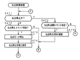
図20および図21は、図13に示された遊技制御処理における入賞球信号処理(ステップS31)の一例を示すフローチャートである。この例では、入賞球信号処理において、まず、払出停止状態であるか否か確認する(ステップS201)。払出停止状態は、払出制御基板37に対して払出停止指示のコマンドを送出した後の状態である。払出停止状態でなければ、上述した球切れ状態フラグまたは満タンフラグがオンになったか否かを確認する(ステップS202)。
20 and 21 are flowcharts showing an example of the winning ball signal process (step S31) in the game control process shown in FIG. In this example, in the winning ball signal processing, first, it is confirmed whether or not the payout is stopped (step S201). The payout stop state is a state after a payout stop instruction command is sent to the
いずれかがオン状態に変化したときには、払出停止指示を示す賞球制御コマンドを出力ポート577(図7参照)に出力し(ステップS203)、INT信号をオン状態にする(ステップS204)。また、5μsのディレイ時間の後(ステップS205)、INT信号をオフ状態にする(ステップS206)。この結果、図19に示されたようなタイミングで、払出停止指示を示す賞球制御コマンドが払出制御基板37に対して送出される。なお、ステップS202において、いずれか一方のフラグが既にオン状態であったときに他方のフラグがオン状態になったときには、払出停止指示を示す賞球制御コマンドの送出制御(ステップS204〜S206)は行われない。
When either of them changes to the on state, a prize ball control command indicating a payout stop instruction is output to the output port 577 (see FIG. 7) (step S203), and the INT signal is turned on (step S204). Further, after a delay time of 5 μs (step S205), the INT signal is turned off (step S206). As a result, a prize ball control command indicating a payout stop instruction is sent to the
また、払出停止状態であれば、球切れ状態フラグおよび満タンフラグがともにオフ状態になったか否かを確認する(ステップS211)。ともにオン状態となったときには、払出停止解除指示を示す賞球制御コマンドを出力ポート577に出力し(ステップS212)、INT信号をオン状態にする(ステップS213)。また、5μsのディレイ時間の後(ステップS214)、INT信号をオフ状態にする(ステップS215)。 If it is in the payout stop state, it is checked whether both the ball-out state flag and the full tank flag are turned off (step S211). When both are turned on, a prize ball control command indicating a payout stop cancellation instruction is output to the output port 577 (step S212), and the INT signal is turned on (step S213). Further, after a delay time of 5 μs (step S214), the INT signal is turned off (step S215).
次いで、CPU56は、入賞に応じた賞球個数を払出制御基板37に送出する制御を行う。この実施の形態では、大入賞口を経た入賞については15個の賞球を払い出し、始動入賞口14を経た入賞については6個の賞球を払い出し、その他の入賞口24および入賞球装置を経た入賞については10個の賞球を払い出すとする。
Next, the
CPU56は、まず、大入賞口用カウンタの値をチェックする(ステップS361)。上述したように、大入賞口用カウンタは、遊技球が大入賞口に入賞してカウントスイッチ23がオンするとカウントアップされる。大入賞口用カウンタの値が0でない場合には、15個の払出個数指示を示す賞球制御コマンドを出力ポート577に出力し(ステップS362)、INT信号をオン状態にする(ステップS363)。また、5μsのディレイ時間の後(ステップS364)、INT信号をオフ状態にする(ステップS365)。そして、大入賞口用カウンタの値を−1し(ステップS366)、払出指令個数累積値に15を加算する(ステップS367)。
First, the
大入賞口用カウンタの値が0であれば、普通入賞口用カウンタの値をチェックする(ステップS371)。上述したように、普通入賞口用カウンタは、遊技球が入賞口に入賞して入賞口スイッチ19a,24aがオンするとカウントアップされる。普通入賞口用カウンタの値が0でない場合には、10個の払出個数指示を示す賞球制御コマンドを出力ポート577に出力し(ステップS372)、INT信号をオン状態にする(ステップS373)。また、5μsのディレイ時間の後(ステップS374)、INT信号をオフ状態にする(ステップS375)。そして、普通入賞口用カウンタの値を−1し(ステップS376)、払出指令個数累積値に10を加算する(ステップS377)。
If the value of the big prize counter is 0, the value of the normal prize counter is checked (step S371). As described above, the counter for the normal winning opening is counted up when the game ball wins the winning opening and the winning
普通入賞口用カウンタの値が0であれば、始動入賞口用カウンタの値をチェックする(ステップS381)。上述したように、始動入賞口用カウンタは、遊技球が始動入賞口に入賞して始動口スイッチ17がオンするとカウントアップされる。始動入賞口用カウンタの値が0でない場合には、6個の払出個数指示を示す賞球制御コマンドを出力ポート577に出力し(ステップS382)、INT信号をオン状態にする(ステップS383)。また、5μsのディレイ時間の後(ステップS384)、INT信号をオフ状態にする(ステップS385)。そして、普通入賞口用カウンタの値を−1し(ステップS386)、払出指令個数累積値に6を加算する(ステップS387)。
If the value of the normal winning port counter is 0, the value of the starting winning port counter is checked (step S381). As described above, the start winning port counter is counted up when the game ball wins the start winning port and the
以上にようにして、遊技制御手段から払出制御基板37に対して、払出制御手段が受信可能に賞球制御コマンドが一回だけ送出される。
As described above, the prize control command is sent only once from the game control means to the
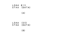
賞球個数を決定するときに、すなわち、払出個数を決定するときに(ステップS362,S372,S382)、CPU56が実行するプログラムにおいて15個、10個または6個を記載してもよいが、この実施の形態では、各個数が、ROM54のデータ領域に記載されている。そして、賞球個数を決定するときに、ROM54におけるデータ領域を参照する。図22にメモリマップの例を示す。この例では、ROM領域はアドレスE000(H)〜FFFF(H)に割り当てられ、ROM領域において、プログラムを含まないデータ領域がE200(H)〜EDFF(H)に割り当てられ、プログラム領域がEE00(H)〜F7FF(H)に割り当てられている。
When determining the number of winning balls, that is, when determining the number of payouts (steps S362, S372, and S382), 15, 10, or 6 may be described in the program executed by the
そして、データ領域中に、賞球個数を示す「15」、「6」、「10」が設定されている。「AA」は「15」が設定されているアドレスのラベルである。 In the data area, “15”, “6”, and “10” indicating the number of prize balls are set. “AA” is a label of an address for which “15” is set.
図23は、賞球個数「15」を決定するときの具体的なプログラム例を示す。図23(A)はプログラムにおいて個数が記載されている例、図23(B)はこの実施の形態で用いられる例を示す。図23(A)に示す例では、即値「15」がアキュムレータにロードされ、その後、アキュムレータの内容がラベルDATAで指定される領域に設定されている。ラベルDATAで指定される領域は、例えば、ステップS362,S372,S382における出力ポート577である。
FIG. 23 shows a specific program example when determining the number of winning balls “15”. FIG. 23A shows an example in which the number is described in the program, and FIG. 23B shows an example used in this embodiment. In the example shown in FIG. 23A, the immediate value “15” is loaded into the accumulator, and then the contents of the accumulator are set in the area specified by the label DATA. The area specified by the label DATA is, for example, the
図23(A)に示すプログラム構成によると、賞球個数を示す「15」がプログラム領域に書き込まれていることになる。そして、賞球個数を変更する場合には、プログラム領域の内容を書き換える必要がある。図23(A)に示された構成は比較的簡単な例であってプログラム変更時に誤りが生じにくいが、プログラム容量節減等のために複雑なプログラム構造になっている場合には、賞球個数を変更する際に、他の部分に悪影響を与えるような変更がなされる可能性がある。 According to the program configuration shown in FIG. 23A, “15” indicating the number of prize balls is written in the program area. When changing the number of prize balls, it is necessary to rewrite the contents of the program area. The configuration shown in FIG. 23 (A) is a relatively simple example, and errors are unlikely to occur when changing a program. However, when the program structure is complicated in order to save program capacity, the number of prize balls When changing, changes that adversely affect other parts may be made.
図23(B)に示す例では、ラベルSSで指定されるデータ領域の内容がアキュムレータにロードされ、その後、アキュムレータの内容がラベルDATAで指定される領域に設定されている。このようなプログラム構成によると、賞球個数を変更する場合には、ラベルSSに対応したデータ領域に設定されている数値を変更するだけでよく、プログラム領域の内容を変更しなくてよい。例えば、15の賞球個数を14個に変更するときには、ラベルSSに対応したデータ領域に設定されている数値を14に変更するだけでよい。 In the example shown in FIG. 23B, the contents of the data area specified by the label SS are loaded into the accumulator, and then the contents of the accumulator are set in the area specified by the label DATA. According to such a program configuration, when changing the number of winning balls, it is only necessary to change the numerical value set in the data area corresponding to the label SS, and it is not necessary to change the contents of the program area. For example, when the number of 15 winning balls is changed to 14, only the numerical value set in the data area corresponding to the label SS needs to be changed to 14.
このように賞球個数を決定する際にデータ領域に設定されている値を参照するように構成しておけば、基本的な遊技内容は変わらないが入賞に応じて払い出される賞球数が異なる遊技機を開発する場合に、プログラム変更に起因する誤りが発生する余地がなくなる。すなわち、より安全に、プログラム変更を行うことができる。 If the configuration is such that the value set in the data area is referenced when determining the number of winning balls in this way, the basic game content will not change, but the number of winning balls to be paid out will differ according to the winnings. When developing a gaming machine, there is no room for errors due to program changes. That is, the program can be changed more safely.
また、ステップS367,S377,S387における払出個数累積値を加算する際の加算値も、データ領域を参照して決定される。 Further, an addition value for adding the payout amount cumulative value in steps S367, S377, and S387 is also determined with reference to the data area.
なお、この実施の形態では、入賞順に関わりなく、入賞に対して賞球個数の多いものから順に払出制御基板37に対して賞球個数が通知されるが、入賞順に賞球個数を通知するようにしてもよい。
In this embodiment, the number of prize balls is notified to the
次に、払出制御用CPU371による払出制御について説明する。図24は、電源監視および電源バックアップのための払出制御用CPU371周りの一構成例を示すブロック図である。図24に示すように、第1の電源監視回路(第1の電源監視手段)からの電圧低下信号が、バッファ回路960を介して払出制御用CPU371のマスク不能割込端子(NMI端子)に接続されている。第1の電源監視回路は、遊技機が使用する各種直流電源のうちのいずれかの電源の電圧を監視して電源電圧低下を検出する回路である。この実施の形態では、VSLの電源電圧を監視して電圧値が所定値以下になるとローレベルの電圧低下信号を発生する。VSLは、遊技機で使用される直流電圧のうちで最大のものであり、この例では+30Vである。従って、払出制御用CPU371は、割込処理によって電源断の発生を確認することができる
Next, payout control by the payout control CPU 371 will be described. FIG. 24 is a block diagram showing a configuration example around the payout control CPU 371 for power supply monitoring and power supply backup. As shown in FIG. 24, the voltage drop signal from the first power supply monitoring circuit (first power supply monitoring means) is connected to the non-maskable interrupt terminal (NMI terminal) of the payout control CPU 371 via the
払出制御基板37には、初期リセット回路975も搭載されているが、この実施の形態では、初期リセット回路975は、第2の電源監視回路(第2の電源監視手段)も兼ねている。すなわち、リセットIC976は、電源投入時に、外付けのコンデンサに容量で決まる所定時間だけ出力をローレベルとし、所定時間が経過すると出力をハイレベルにする。また、リセットIC976は、電源基板910に搭載されている第1の電源監視回路が監視する電源電圧と等しい電源電圧であるVSLの電源電圧を監視して電圧値が所定値(例えば+9V)以下になるとローレベルの電圧低下信号を発生する。従って、電源断時には、リセットIC976からの電圧低下信号がローレベルになることによって払出制御用CPU371がシステムリセットされる。なお、図24に示すように、電圧低下信号はリセット信号と同じ出力信号である。
Although the
リセットIC976が電源断を検知するための所定値は、通常時の電圧より低いが、払出制御用CPU371が暫くの間動作しうる程度の電圧である。また、リセットIC976が、払出制御用CPU371が必要とする電圧(この例では+5V)よりも高い電圧を監視するように構成されているので、払出制御用CPU371が必要とする電圧に対して監視範囲を広げることができる。従って、より精密な監視を行うことができる。
The predetermined value for the
+5V電源から電力が供給されていない間、払出制御用CPU371の内蔵RAMの少なくとも一部は、電源基板から供給されるバックアップ電源がバックアップ端子に接続されることによってバックアップされ、遊技機に対する電源が断しても内容は保存される。そして、+5V電源が復旧すると、初期リセット回路975からリセット信号が発せられるので、払出制御用CPU371は、通常の動作状態に復帰する。そのとき、必要なデータがバックアップされているので、停電等からの復旧時には停電発生時の遊技状態に復帰することができる。
While power is not supplied from the + 5V power supply, at least a part of the built-in RAM of the payout control CPU 371 is backed up by connecting the backup power supplied from the power supply board to the backup terminal, and the power to the gaming machine is cut off. The contents are saved. When the +5 V power supply is restored, a reset signal is issued from the
以上のように、この実施の形態では、電源基板910に搭載されている第1の電源監視回路が、遊技機で使用される直流電圧のうちで最も高い電源VSLの電圧を監視して、その電源の電圧が所定値を下回ったら電圧低下信号(電源断検出信号)を発生する。電源断検出信号が出力されるタイミングでは、IC駆動電圧は、まだ各種回路素子を十分駆動できる電圧値になっている。従って、IC駆動電圧で動作する払出制御基板37の払出制御用CPU371が所定の電力供給停止時処理を行うための動作時間が確保されている。
As described above, in this embodiment, the first power supply monitoring circuit mounted on the
なお、ここでも、第1の電源監視回路は、遊技機で使用される直流電圧のうちで最も高い電源VSLの電圧を監視することになるが、電源断検出信号を発生するタイミングが、IC駆動電圧で動作する電気部品制御手段が所定の電力供給停止時処理を行うための動作時間が確保されるようなタイミングであれば、監視対象電圧は、最も高い電源VSLの電圧でなくてもよい。すなわち、少なくともIC駆動電圧よりも高い電圧を監視すれば、電気部品制御手段が所定の電力供給停止時処理を行うための動作時間が確保されるようなタイミングで電源断検出信号を発生することができる。 Also in this case, the first power supply monitoring circuit monitors the voltage of the highest power supply VSL among the DC voltages used in the gaming machine, but the timing of generating the power supply interruption detection signal is the IC drive. The monitoring target voltage may not be the voltage of the highest power supply VSL as long as the operation time required for the electric component control means operating at the voltage to perform the predetermined power supply stop process is ensured. That is, if at least a voltage higher than the IC drive voltage is monitored, the power-off detection signal may be generated at such a timing that the operation time for the electric component control means to perform the predetermined power supply stop process is ensured. it can.
その場合、上述したように、監視対象電圧は、賞球カウントスイッチ301A等の遊技機の各種スイッチに供給される電圧が+12Vであることから、電源断時のスイッチオン誤検出の防止も期待できる電圧であることが好ましい。すなわち、スイッチに供給される電圧(スイッチ電圧)である+12V電源電圧が落ち始める以前の段階で、電圧低下を検出できることが好ましい。よって、少なくともスイッチ電圧よりも高い電圧を監視することが好ましい。
In this case, as described above, since the voltage supplied to various switches of the gaming machine such as the prize
なお、図24に示された構成では、初期リセット回路975は、電源投入時に、コンデンサの容量で決まる期間のローレベルを出力し、その後ハイレベルを出力する。すなわち、リセット解除タイミングは1回だけである。しかし、図8に示された主基板31の場合と同様に、複数回のリセット解除タイミングが発生するような回路構成を用いてもよい。
In the configuration shown in FIG. 24, the
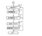
図25は、払出制御用CPU371のメイン処理を示すフローチャートである。メイン処理では、払出制御用CPU371は、まず、RAM領域をクリアする等の初期値設定処理を行う(ステップS701)。なお、内蔵RAMの電源バックアップされたRAM領域(バックアップRAM領域)にデータが設定されている場合には、それらの領域のクリア処理はなされない。その後、この実施の形態では、払出制御用CPU371は、タイマ割込フラグの監視(ステップS702)の確認を行うループ処理に移行する。 FIG. 25 is a flowchart showing main processing of the payout control CPU 371. In the main process, the payout control CPU 371 first performs an initial value setting process such as clearing the RAM area (step S701). When data is set in the RAM area (backup RAM area) backed up by the power supply of the built-in RAM, the clearing process of those areas is not performed. Thereafter, in this embodiment, the payout control CPU 371 shifts to a loop process for checking the timer interrupt flag (step S702).
ステップS701の初期化処理では、後述する総合個数記憶および貸し玉個数記憶の値が0でない場合には、非バックアップRAM領域をクリアする。そして、賞球再開のための設定を行う。例えば、賞球中処理中フラグのセット等を行う。なお、バックアップRAM領域であっても、賞球個数に関わらない領域であるならば、それらのアドレスを指定してクリアするようにしてもよい。さらに、それら処理の他に、2ms毎に定期的にタイマ割込がかかるように払出制御用CPU371に設けられているタイマレジスタの初期設定(タイムアウトが2msであることと繰り返しタイマが動作する設定)が行われる。すなわち、タイマ割込を能動化する処理と、タイマ割込インタバルを設定する処理とが実行される。 In the initialization process in step S701, the non-backup RAM area is cleared if the values of the total number storage and the lending ball number storage described later are not 0. Then, settings for restarting the prize ball are made. For example, an in-price ball processing flag is set. Even if it is a backup RAM area, if it is an area not related to the number of winning balls, it may be cleared by designating those addresses. In addition to these processes, initial setting of a timer register provided in the payout control CPU 371 so that a timer interrupt is periodically generated every 2 ms (timeout is 2 ms and setting for repeated timer operation) Is done. That is, processing for activating a timer interrupt and processing for setting a timer interrupt interval are executed.
従って、この実施の形態では、払出制御用CPU371の内部タイマが繰り返しタイマ割込を発生するように設定される。この実施の形態では、繰り返し周期は2msに設定される。そして、図26に示すように、タイマ割込が発生すると、払出制御用CPU371は、タイマ割込フラグをセットする(ステップS711)。 Therefore, in this embodiment, the internal timer of the payout control CPU 371 is set to repeatedly generate a timer interrupt. In this embodiment, the repetition period is set to 2 ms. Then, as shown in FIG. 26, when a timer interrupt occurs, the payout control CPU 371 sets a timer interrupt flag (step S711).
払出制御用CPU371は、ステップS702において、タイマ割込フラグがセットされたことを検出すると、タイマ割込フラグをリセットするとともに(ステップS703)、払出制御処理を実行する(ステップS705)。以上の制御によって、この実施の形態では、払出制御処理は2ms毎に起動されることになる。なお、この実施の形態では、タイマ割込処理ではフラグセットのみがなされ、払出制御処理はメイン処理において実行されるが、タイマ割込処理で払出制御処理を実行してもよい。 When detecting that the timer interrupt flag is set in step S702, the payout control CPU 371 resets the timer interrupt flag (step S703) and executes a payout control process (step S705). With the above control, in this embodiment, the payout control process is started every 2 ms. In this embodiment, only the flag is set in the timer interrupt process, and the payout control process is executed in the main process, but the payout control process may be executed in the timer interrupt process.
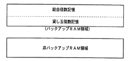
図27は、払出制御用CPU371が内蔵するRAMの使用例を示す説明図である。この例では、バックアップRAM領域に総合個数記憶(例えば2バイト)および貸し玉個数記憶が形成されている。総合個数記憶は、主基板31の側から指示された払出個数の総数を記憶するものである。貸し玉個数記憶は、未払出の球貸し個数を記憶するものである。なお、バックアップRAM領域には、各種フラグ類を設定するための領域もある。また、図27では、非バックアップ領域も示されているが、払出制御用CPU371が内蔵するRAMは全て電源バックアップされていてもよい。
FIG. 27 is an explanatory diagram showing a usage example of the RAM built in the payout control CPU 371. In this example, a total number storage (for example, 2 bytes) and a rental ball number storage are formed in the backup RAM area. The total number storage stores the total number of payouts instructed from the
図28は、割込処理による賞球制御コマンド受信処理を示すフローチャートである。主基板31からの賞球制御INT信号は払出制御用CPU371の割込端子に入力されている。よって、主基板31からの賞球制御INT信号がオン状態になると、払出制御用CPU371に割込がかかり、図28に示す賞球制御コマンドの受信処理が開始される。
FIG. 28 is a flowchart showing a prize ball control command reception process by an interrupt process. The prize ball control INT signal from the
賞球制御コマンドの受信処理において、払出制御用CPU371は、まず、賞球制御コマンドデータの入力に割り当てられている入力ポートから1バイトのデータを読み込む(ステップS852)。読み込んだデータが払出個数指示コマンドであれば(ステップS853)、払出個数指示コマンドで指示された個数を総合個数記憶に加算する(ステップS855)。そうでなければ、通信終了フラグをセットする(ステップS854)。なお、通信終了フラグは、この例では、払出個数指示コマンド以外のコマンドを受信したことを示すフラグである。 In the prize ball control command reception process, the payout control CPU 371 first reads 1-byte data from the input port assigned to the prize ball control command data input (step S852). If the read data is a payout number instruction command (step S853), the number specified by the payout number instruction command is added to the total number memory (step S855). Otherwise, a communication end flag is set (step S854). In this example, the communication end flag is a flag indicating that a command other than the payout number instruction command has been received.
以上のように、払出制御基板37に搭載された払出制御用CPU371は、主基板31のCPU56から送られた払出個数指示コマンドに含まれる賞球数をバックアップRAM領域(総合個数記憶)に記憶する。
As described above, the payout control CPU 371 mounted on the
図29〜図32は、払出制御処理(ステップS705)の一例を示すフローチャートである。この例では、払出制御用CPU371は、まず、払出停止中であるか否か確認する(ステップS471)。払出停止中でなければ、主基板31から払出停止指示を示す賞球制御コマンドを受信したか否か確認する(ステップS472)。受信していれば、払出モータ289を停止するとともに(ステップS473)、内部状態を払出停止状態に設定する(ステップS474)。すなわち、払出制御手段は、賞球払出も球貸しも停止する状態になる。
29 to 32 are flowcharts illustrating an example of the payout control process (step S705). In this example, the payout control CPU 371 first checks whether or not payout is stopped (step S471). If the payout is not stopped, it is confirmed whether or not a prize ball control command indicating a payout stop instruction is received from the main board 31 (step S472). If it has been received, the
なお、この実施の形態では、払出停止指示のコマンドを受信したら直ちに払出モータ289を停止するが、そのように制御するのではなく、切りのよいところで払出モータ289を停止するようにしてもよい。例えば、遊技球の払出を25個単位で実行し、一単位の払出が完了した時点で払出モータ289を停止するとともに、内部状態を払出停止状態に設定するようにしてもよい。上述したように、球切れスイッチ187a,187bは、払出球通路186a,186bに27〜28個程度の遊技球が存在することを検出できるような位置に設置されているので、主基板31の遊技制御手段が球切れを検出しても、その時点から少なくとも25個の払出は可能である。従って、一単位の払出が完了した時点で払出停止状態にしても問題は生じない。また、一単位の区切りで払出停止状態とすれば、払出再開時の制御が容易になる。
In this embodiment, the
払出停止状態であれば、払出制御用CPU371は、主基板31から払出停止解除指示を示す賞球制御コマンドを受信したか否か確認する(ステップS475)。受信していなければ、ステップS471に戻る。払出停止解除指示を示す賞球制御コマンドを受信していれば、内部状態の払出停止状態を解除する(ステップS476)。すなわち、払出制御手段は、賞球払出および球貸しができる状態に戻る。 If it is in the payout stop state, the payout control CPU 371 checks whether or not a prize ball control command indicating a payout stop cancellation instruction has been received from the main board 31 (step S475). If not received, the process returns to step S471. If a prize ball control command indicating a payout stop cancellation instruction has been received, the internal payout stop state is canceled (step S476). That is, the payout control means returns to a state where the prize ball can be paid out and lent out.
払出停止状態でなければ、払出制御用CPU371は、ステップS481以降の処理を行う。ステップS481において、払出制御用CPU371は、現在球貸し中であるか否か確認する。球貸し中であれば、ステップS532の球貸し中の処理に移行する。球貸し中でない場合には、賞球処理中であるか否か確認する(ステップS482)。賞球処理中であれば、ステップS513の賞球処理中の処理に移行する。 If it is not in the payout stop state, the payout control CPU 371 performs the processing after step S481. In step S481, the payout control CPU 371 checks whether or not the ball is currently being lent. If the ball is being lent, the process proceeds to the process of renting the ball in step S532. If the ball is not being lent, it is confirmed whether or not the prize ball is being processed (step S482). If the prize ball process is in progress, the process proceeds to the process during the prize ball process in step S513.
賞球処理中でもなければ、遊技機の外部機器としてのカードユニット50からの球貸し要求信号であるBRQ信号がオンになっているかどうか確認する(ステップS483)。BRQ信号がオンになっていれば、ステップS491以降の処理を行う。BRQ信号がオンになっていなければ、すなわち球貸し要求が発生していなければ、総合個数記憶が0であるか否か確認する(ステップS491)。総合個数記憶が0であれば、すなわち、賞球払出を開始する必要がない場合には、処理を終了する。 If the winning ball processing is not in progress, it is confirmed whether or not the BRQ signal, which is a ball lending request signal from the card unit 50 as an external device of the gaming machine, is turned on (step S483). If the BRQ signal is on, the processing from step S491 is performed. If the BRQ signal is not turned on, that is, if a ball lending request is not generated, it is confirmed whether or not the total number storage is 0 (step S491). If the total number storage is 0, that is, if it is not necessary to start paying out a prize ball, the process is terminated.
なお、この実施の形態では、ステップS481〜S491の判断によって球貸しが賞球処理よりも優先されることになるが、賞球処理が球貸しに優先するようにしてもよい。 In this embodiment, the ball lending is prioritized over the winning ball processing according to the determinations in steps S481 to S491, but the winning ball processing may be prioritized over the ball lending.
ステップS492において、払出制御用CPU371は、球貸し処理中フラグをオンし、球貸し個数カウンタに単位数を設定して(ステップS493)、EXS信号をオンする(ステップS494)。単位数は、例えば所定単位である100円で貸し出される遊技球の数(例えば25個)である。そして。球払出装置97の下方の球振分部材311を球貸し側に設定するために振分用ソレノイド310を駆動する(ステップS495)。また、払出モータ289をオンして(ステップS496)、図32に示す球貸し中の処理に移行する。
In step S492, the payout control CPU 371 turns on the ball lending process flag, sets the unit number in the ball lending number counter (step S493), and turns on the EXS signal (step S494). The number of units is, for example, the number (for example, 25) of game balls lent out at a predetermined unit of 100 yen. And then. In order to set the
なお、払出モータ289をオンするのは、厳密には、カードユニット50が受付を認識したことを示すためにBRQ信号をOFFとしてからである。また、球貸し個数カウンタはバックアップRAM領域の貸し玉個数記憶に形成されている。また、球貸し処理中フラグもバックアップRAM領域に設定される。
Strictly speaking, the
ステップS491において総合個数記憶が0でなければ、賞球払出を開始する処理を行う。すなわち、賞球処理中フラグをオンし(ステップS505)、球払出装置97の下方の球振分部材311を賞球側に設定し(ステップS506)、払出モータ289をオンする(ステップS507)。そして、賞球払出中処理に移行する。なお、賞球処理中フラグは、バックアップRAM領域に設定される。
If the total number storage is not 0 in step S491, a process for starting a prize ball payout is performed. That is, the award ball processing flag is turned on (step S505), the
ステップS513以降の処理は賞球払出中の処理である。賞球払出中の処理において、払出制御用CPU371は、賞球カウントスイッチ301Aの検出出力によって遊技球の払出がなされたか否かの確認を行う。そして、1個の払出が行われたことを確認したら(ステップS513)、総合個数記憶の値を−1する(ステップS514)。また、総合個数記憶の値が0になったら(ステップS515)、払出モータ289をオフするとともに(ステップS516)、賞球処理中フラグをオフする(ステップS517)。
The process after step S513 is a process during payout of a prize ball. In the process of paying out a prize ball, the payout control CPU 371 checks whether or not a game ball has been paid out based on the detection output of the prize
総合個数記憶の内容は、遊技機の電源が断しても、所定期間電源基板910のバックアップ電源によって保存される。従って、所定期間中に電源が回復すると、払出制御用CPU371は、総合個数記憶の内容にもとづいて賞球払出処理を継続することができる。
The contents of the total number storage are saved by the backup power source of the
払出制御用CPU371は、電源投入時に、バックアップRAM領域のデータを確認するだけで、通常の初期設定処理を行うのか賞球中の状態を復元するのか決定できる。すなわち、簡単な判断によって、未払出賞球について賞球処理再開を行うことができる。 When the power is turned on, the payout control CPU 371 can determine whether to perform normal initial setting processing or restore the state in the winning ball simply by checking the data in the backup RAM area. In other words, it is possible to resume the prize ball processing for the unpaid prize balls by simple determination.
なお、払出制御用CPU371は、主基板31から指示された賞球個数を総合個数記憶で総数として管理したが、賞球数毎(例えば15個、10個、6個)に管理してもよい。例えば、賞球数毎に対応した個数カウンタを設け、払出個数指定コマンドを受信すると、そのコマンドで指定された個数に対応する個数カウンタを+1する。そして、賞球数毎の賞球払出が終了すると、対応する個数カウンタを−1する。その場合にも、各個数カウンタはバックアップRAM領域に形成される。よって、遊技機の電源が断しても、所定期間中に電源が回復すれば、払出制御用CPU371は、各個数カウンタの内容にもとづいて賞球払出処理を継続することができる。
The payout control CPU 371 manages the number of prize balls instructed from the
図32は、払出制御用CPU371による払出制御処理における球貸し中の処理を示すフローチャートである。球貸し処理において、払出制御用CPU371は、球貸しカウントスイッチ301Bの検出出力によって遊技球の払出がなされたか否かの確認を行う。そして、1個の払出が行われたことを確認したら(ステップS532)、球貸し個数カウンタの値を−1する(ステップS533)。また、球貸し個数カウンタの値が0になったら(ステップS534)、カードユニット50に対して、次の球貸し要求の受付が可能になったことを示すためにEXS信号をオフにする(ステップS535)。また、払出モータ289をオフするとともに(ステップS535)、球貸し処理中フラグをオフする(ステップS537)。
FIG. 32 is a flowchart showing a ball lending process in the payout control process by the payout control CPU 371. In the ball lending process, the payout control CPU 371 checks whether or not a game ball has been paid out based on the detection output of the ball lending
なお、球貸し要求の受付を示すEXS信号をオフにした後、所定期間内に再び球貸し要求信号であるBRQ信号がオンしたら、払出モータをオフせずに球貸し処理を続行するようにしてもよい。すなわち、所定単位(この例では100円単位)毎に球貸し処理を行うのではなく、球貸し処理を連続して実行するように構成することもできる。 After turning off the EXS signal indicating acceptance of a ball lending request, if the BRQ signal, which is a ball lending request signal, is turned on again within a predetermined period, the ball lending process is continued without turning off the payout motor. Also good. That is, instead of performing the ball lending process for each predetermined unit (100 yen unit in this example), the ball lending process may be executed continuously.
貸し玉個数記憶の内容は、遊技機の電源が断しても、所定期間電源基板910のバックアップ電源によって保存される。従って、所定期間中に電源が回復すると、払出制御用CPU371は、貸し玉個数記憶の内容にもとづいて球貸し処理を継続することができる。
The contents of the number of lent balls are stored by the backup power source of the
図33は、払出制御用CPU371が第1の電源監視手段からの割込に応じて実行される停電発生割込処理を示すフローチャートである。電源基板910の電源監視用IC902が電源電圧の低下を検出すると電圧低下信号が電圧低下を示す状態となり、停電発生割込処理が開始される。停電発生割込処理において、払出制御用CPU371は、割込禁止に設定し(ステップS801)、RAMアクセス禁止状態に設定し(ステップS802)、出力ポートをオフ状態にして(ステップS803)、ループ処理に入る。すなわち、何らの処理もしない状態になる。
FIG. 33 is a flowchart showing a power failure occurrence interrupt process executed by the payout control CPU 371 in response to an interrupt from the first power supply monitoring unit. When the
従って、図24に示されたリセットIC976からのリセット信号によって外部から動作禁止状態(システムリセット)にされる前に、内部的に動作停止状態になる。よって、電源断時に確実に払出制御用CPU371は動作停止する。その結果、電源電圧が低下していくことに伴って生ずる可能性がある異常動作に起因するRAMの内容破壊等を確実に防止することができる。
Therefore, before the operation is prohibited (system reset) from the outside by the reset signal from the
なお、この実施の形態では、停電発生割込処理では最終部でプログラムをループ状態にしたが、ホールト(HALT)命令を発行するように構成してもよい。また、割込処理中には他の割込がかからないような仕様のCPUを用いた場合にはステップS801の処理は不要である。また、この実施の形態では、停電発生割込処理(電力供給停止時処理)はNMIに応じて実行されるが、電源基板からの第1の電圧低下信号(第1の電源監視手段からの電圧低下信号)をマスク可能割込割込端子(IRQ端子)に導入して、割込処理(IRQ処理)で電力供給停止時処理を実行してもよい。 In this embodiment, in the power failure occurrence interrupt process, the program is looped at the final part, but a halt (HALT) instruction may be issued. Further, when a CPU having a specification that does not cause other interrupts during the interrupt process is used, the process of step S801 is not necessary. Further, in this embodiment, the power failure occurrence interrupt process (power supply stop process) is executed according to the NMI, but the first voltage drop signal from the power supply board (the voltage from the first power supply monitoring means). A reduction signal) may be introduced into the maskable interrupt terminal (IRQ terminal) and the power supply stop process may be executed by the interrupt process (IRQ process).
図34は、払出制御用CPU371が電源投入時に実行する初期化処理(ステップS701)の一部を示すフローチャートである。電源が投入され、または、電源が復旧したときには、払出制御用CPU371は、まず、バックアップRAM領域に形成されている総合個数記憶または貸し玉個数記憶の値が0でないかどうか確認する(ステップS901)。0である場合には、前回の電源オフ時に未払出賞球はなかったことになるので、通常の初期設定処理を行う。すなわち、レジスタおよび全RAM領域をクリアして(ステップS903)、スタックポインタの初期設定を行う(ステップS904)。 FIG. 34 is a flowchart showing a part of the initialization process (step S701) executed by the payout control CPU 371 when the power is turned on. When the power is turned on or the power is restored, the payout control CPU 371 first checks whether the value of the total number storage or the number of rented balls stored in the backup RAM area is not 0 (step S901). . If it is 0, it means that there was no unpaid prize ball at the time of the previous power-off, so normal initial setting processing is performed. That is, the register and the entire RAM area are cleared (step S903), and the stack pointer is initialized (step S904).
総合個数記憶または貸し玉個数記憶の値が0でない場合には、アドレスを指定してレジスタと非バックアップRAM領域をクリアする(ステップS905)。そして、賞球または球貸し再開のための設定を行う。例えば、球貸し処理中フラグのセット等を行う(ステップS906)。なお、バックアップRAM領域であっても、賞球個数に関わらない領域であるならば、それらのアドレスを指定してクリアするようにしてもよい。 If the value of the total number storage or the lending ball number storage is not 0, an address is designated and the register and the non-backup RAM area are cleared (step S905). Then, a setting for resuming a prize ball or ball lending is performed. For example, a ball lending process flag is set (step S906). Even if it is a backup RAM area, if it is an area not related to the number of winning balls, it may be cleared by designating those addresses.
このように、払出制御用CPU371は、電源投入時に、バックアップRAM領域のデータを確認するだけで、通常の初期設定処理を行うのか賞球払出中または球貸し中の状態を復元するのか決定できる。つまり、未払出の遊技球数および賞球処理中フラグと球貸し処理中フラグとはバックアップRAMに保存されているので、払出制御用CPU371は、賞球処理中フラグまたは球貸し処理中フラグがセットされていれば、総合個数記憶または貸し玉個数記憶の内容に応じた処理を続行することができる。すなわち、簡単な判断によって、未払出賞球または未払出貸し玉について処理再開を行うことができる。 As described above, the payout control CPU 371 can determine whether to perform normal initial setting processing or to restore the state in which a prize ball is being paid out or being lent out by simply checking the data in the backup RAM area when the power is turned on. That is, since the number of unpaid game balls and the winning ball processing flag and the ball lending processing flag are stored in the backup RAM, the payout control CPU 371 sets the award ball processing flag or the ball lending processing flag. If so, the processing corresponding to the contents of the total number storage or the rental ball number storage can be continued. That is, processing can be resumed for unpaid prize balls or unpaid lending balls by simple determination.
上記の実施の形態では、バックアップRAM領域の貸し玉個数記憶に記憶されている球貸しに関する情報は、球貸し個数カウンタの値である。すなわち、1回の所定単位(この例では100円に対応する単位数:25個)における未払出遊技球数である。しかし、複数回の所定単位の全てについての未払出貸し玉数を貸し玉個数記憶に記憶してもよい。その場合、例えば、500円分の球貸しの要求、すなわち、所定単位の5回分の球貸し要求を、払出制御用CPU371は、あらかじめ全て受け付け、所定単位5回分の球貸しを行うべき旨の情報をバックアップRAM領域の貸し玉個数記憶に記憶する。 In the above embodiment, the information related to the ball lending stored in the lending ball number storage in the backup RAM area is the value of the ball lending number counter. That is, the number of unpaid game balls in one predetermined unit (in this example, the number of units corresponding to 100 yen: 25). However, the number of unpaid lending balls for all of the predetermined units may be stored in the lending ball number storage. In this case, for example, information indicating that the payout control CPU 371 should accept all the lending requests for 500 yen, that is, the lending requests for 5 times in a predetermined unit, and perform lending for 5 times in a predetermined unit. Is stored in the rental ball number storage in the backup RAM area.
そのような制御によって、カードユニット50から所定回連続して球貸し要求が出力される場合に、全ての要求が順次受け付けられる。そして、受け付けたが、その受付に対してまだ払い出しが開始されていないものについては球貸し回数カウンタの値に保存される。 With such control, when a ball lending request is continuously output from the card unit 50 a predetermined number of times, all requests are sequentially accepted. Then, those that have been accepted but have not yet started to be paid out are saved in the value of the ball lending counter.
球貸し回数カウンタおよび球貸し個数カウンタの値はバックアップRAM領域における貸し玉個数記憶に記憶されるので、遊技機に対する電源が断しても所定期間は保存される。そして、その所定期間内に電源が回復すれば、払出制御用CPU371は、保存されている球貸し回数カウンタおよび球貸し個数カウンタの値にもとづいて球貸し処理を続行することができる。すなわち、払出制御手段が、複数回の球貸し要求を全て受け付けて、その後に順次球貸し処理を実行するように構成されている場合でも、遊技者に対して球貸しに関する不利益を与えることのない制御が実現される。 Since the value of the ball lending number counter and the ball lending number counter are stored in the lending ball number storage in the backup RAM area, they are stored for a predetermined period even when the power to the gaming machine is cut off. If the power supply is restored within the predetermined period, the payout control CPU 371 can continue the ball lending process based on the stored values of the ball lending number counter and the ball lending number counter. In other words, even when the payout control means is configured to accept all ball lending requests multiple times and then sequentially execute the ball lending process, the player may be disadvantaged with respect to ball lending. No control is realized.
また、複数回の球貸し要求の受付が開始されると同時に実際の球貸し処理も開始されるように構成してもよいが、事前に複数回の球貸し要求を全て受け付け、受付完了後に実際の球貸し処理を開始するように構成してもよい。 In addition, it may be configured so that the actual ball lending process is started at the same time as the acceptance of a plurality of ball lending requests is started. The ball lending process may be started.
また、上記の実施の形態では、停電等の電源断が生じたときの電力供給停止時処理として単にRAMアクセス禁止を行っただけであるが、RAM内のデータを対象としてパリティデータを作成し、作成したパリティデータも保存するようにしてもよい。そして、電源投入時の処理において、パリティデータにもとづく確認を行い、RAM内のデータが正しく保存されていたことを確認したら、保存されているデータにもとづく賞球払出処理または球貸し処理を続行するようにしてもよい。 In the above embodiment, the RAM access is simply prohibited as the power supply stop process when a power interruption such as a power failure occurs, but the parity data is created for the data in the RAM, The created parity data may also be saved. Then, at the time of power-on processing, confirmation based on the parity data is performed, and if it is confirmed that the data in the RAM is correctly stored, the winning ball payout processing or ball lending processing based on the stored data is continued. You may do it.
以上に説明したように、この実施の形態では、払い出される遊技球の不足が検知されたとき(球切れ時)にも、下皿満タンで遊技球を払い出すべきでないときの、同一のコマンドである払出停止指示のコマンドが遊技制御手段から払出制御手段に通知される(図20参照)。そして、払出制御手段は、払出停止指示に応じて賞球払出を停止する。すなわち、賞球停止をすべき条件が異なっていても、共通のコマンドが遊技制御手段から払出制御手段に送出される。従って、遊技制御手段から払出制御手段に対する情報伝達に関する負荷が低減される。その結果、遊技制御手段におけるプログラム容量が節減されて遊技制御に回せるプログラム容量が増える等の利点が生ずる。 As described above, in this embodiment, even when a shortage of game balls to be paid out is detected (when a ball is out of service), the same command is used when the game ball should not be paid out when the lower plate is full. The payout stop command is notified from the game control means to the payout control means (see FIG. 20). Then, the payout control means stops the prize ball payout according to the payout stop instruction. That is, even if the conditions for stopping the prize ball are different, a common command is sent from the game control means to the payout control means. Therefore, a load related to information transmission from the game control means to the payout control means is reduced. As a result, there is an advantage that the program capacity in the game control means is reduced and the program capacity that can be used for game control is increased.
また、球切れ解除についても、下皿満タンの解消についても、同一のコマンドである払出停止解除指示のコマンドが遊技制御手段から払出制御手段に通知される。そして、払出制御手段は、払出停止指示に応じて賞球払出を可能な状態に戻す。すなわち、賞球停止解除の原因が異なっていても、共通のコマンドが遊技制御手段から払出制御手段に送出される。その結果、やはり、遊技制御手段から払出制御手段に対する情報伝達に関する負荷が低減される。 In addition, the game control means notifies the payout control means of a payout stop release command, which is the same command for releasing the ball breakage and for solving the lower pan full. Then, the payout control means returns to a state in which the prize ball can be paid out according to the payout stop instruction. That is, even if the cause of the award ball stop cancellation is different, a common command is sent from the game control means to the payout control means. As a result, the load related to information transmission from the game control means to the payout control means is also reduced.
また、払出制御手段は、払出停止指示に応じて球貸しを停止する。すなわち、球貸し停止をすべき条件が異なっていても、共通のコマンドが遊技制御手段から払出制御手段に送出される。従って、遊技制御手段から払出制御手段に対する情報伝達に関する負荷が低減される。その結果、遊技制御手段におけるプログラム容量が節減されて遊技制御に回せるプログラム容量が増える等の利点が生ずる。 Further, the payout control means stops the ball lending according to the payout stop instruction. That is, a common command is sent from the game control means to the payout control means even if the conditions for stopping lending are different. Therefore, a load related to information transmission from the game control means to the payout control means is reduced. As a result, there is an advantage that the program capacity in the game control means is reduced and the program capacity that can be used for game control is increased.
そして、払出制御手段は、払出停止指示に応じて球貸しを可能な状態に戻す。すなわち、球貸し停止解除の原因が異なっていても、共通のコマンドが遊技制御手段から払出制御手段に送出される。その結果、やはり、遊技制御手段から払出制御手段に対する情報伝達に関する負荷が低減される。 Then, the payout control means returns the ball lending to a possible state according to the payout stop instruction. That is, even if the causes of the ball lending stop cancellation are different, a common command is sent from the game control means to the payout control means. As a result, the load related to information transmission from the game control means to the payout control means is also reduced.
なお、上記の実施の形態では、払出制御手段は払出停止指示のコマンドを受信すると球貸しも賞球払出もともに停止し、払出停止解除指示に応じて球貸しも賞球払出もともに可能な状態に戻したが、賞球に関する払出停止指示と球貸しに関する払出停止指示とを別コマンドとし、賞球に関する払出停止解除指示と球貸しに関する払出停止解除指示とを別コマンドとしてもよい。その場合でも、賞球停止/停止解除をすべき条件が異なっていても共通のコマンドが遊技制御手段から払出制御手段に送出され、球貸し停止/停止解除をすべき条件が異なっていても共通のコマンドが遊技制御手段から払出制御手段に送出されるように構成することができる。 In the above embodiment, when the payout control means receives the payout stop command, both the ball lending and the prize ball payout are stopped, and both the ball lending and the prize ball payout are possible according to the payout stop cancellation instruction. However, the payout stop instruction for the winning ball and the payout stop instruction for the ball lending may be separate commands, and the payout stop canceling instruction for the prize ball and the payout stop canceling instruction regarding the ball lending may be separate commands. Even in such a case, a common command is sent from the game control means to the payout control means even if the conditions for stopping and releasing the winning ball are different, and common even if the conditions for stopping and releasing the ball rental are different. This command can be sent from the game control means to the payout control means.
しかし、払出制御手段が払出停止指示のコマンドを受信すると、球貸しも賞球払出もともに停止し、払出停止解除指示のコマンドを受信すると、球貸しも賞球払出もともに可能な状態にすれば、すなわち、1つのコマンドで、球貸しも賞球払出も停止し、また、停止状態を解除すれば、それぞれについての停止指示コマンドおよび停止解除指示コマンドを用いる場合に比べて遊技制御手段から払出制御手段に対する情報伝達に関する負荷がさらに低減される。 However, when the payout control means receives a payout stop instruction command, both the ball lending and prize ball payout are stopped, and when a payout stop release instruction command is received, both the ball lending and prize ball payout are enabled. That is, with one command, ball lending and prize ball payout are stopped, and if the stop state is canceled, the payout control from the game control means is performed as compared with the case of using the stop instruction command and the stop release instruction command for each. The load related to information transmission to the means is further reduced.
なお、上記の実施の形態では、払出手段は球貸しも賞球払出も行える構成であったが、球貸しを行う機構と賞球払出を行う機構とが独立していても本発明を適用することができる。その場合、球貸しを行う機構と賞球払出を行う機構とが独立していても、払出制御手段が両方の機構を制御するように構成されていれば、上記の実施の形態のように1つのコマンドで球貸しも賞球払出も停止/停止解除を指示するように構成することがより有効になる。 In the above embodiment, the payout means is configured to be able to lend a ball and a prize ball. However, the present invention is applied even if a mechanism for lending a ball and a mechanism for paying a prize ball are independent. be able to. In that case, even if the mechanism that lends the ball and the mechanism that pays out the prize ball are independent, if the payout control means is configured to control both mechanisms, 1 as in the above embodiment. It is more effective to configure the ball lending and the winning ball payout to be instructed to stop / release with one command.
また、遊技制御手段において、入賞に応じた賞球個数を決定する場合にプログラムには個数が直接記述されていず、データ領域が参照されることによって、賞球個数が決定される。よって、入賞に応じた賞球個数が異なる機種を開発するときでも、データ変更が容易である。なお、上記の実施の形態では、遊技機として第1種パチンコ遊技機を例にしたが、本発明は他のタイプのパチンコ遊技機や他の遊技機例えばスロット機にも適用可能である。例えば、スロット機において、賞球として払い出されるメダル数をデータ領域に記載しておけば、賞球個数が異なる機種を開発するときでも、データ変更が容易である。 In the game control means, when determining the number of winning balls according to the winning, the number is not directly described in the program, and the number of winning balls is determined by referring to the data area. Therefore, data can be easily changed even when developing models with different numbers of winning balls according to winning. In the above embodiment, the first type pachinko gaming machine is taken as an example of the gaming machine, but the present invention is also applicable to other types of pachinko gaming machines and other gaming machines such as slot machines. For example, in a slot machine, if the number of medals to be paid out as a prize ball is described in the data area, it is easy to change data even when developing a model with a different number of prize balls.
31 遊技制御基板(主基板)
37 払出制御基板
53 基本回路
56 CPU
97 球払出装置
301A 賞球カウントスイッチ
301B 球貸しカウントスイッチ
371 払出制御用CPU
31 Game control board (main board)
37
97
Claims (1)
電力が供給される状態になったときに、電力供給停止直前の内容を保持することが可能な記憶手段に保持されている記憶内容にもとづいて遊技状態を復帰させる遊技状態復帰制御を行うことが可能であり、
遊技の進行を制御する遊技制御手段と、
遊技媒体を検出するための遊技媒体検出手段と、
前記遊技媒体検出手段に供給される電圧よりも高い電源電圧を監視し、該電源電圧が所定値以下になったことにより電圧低下信号を前記遊技制御手段に出力する電源監視手段とを備え、
前記遊技制御手段は、遊技制御マイクロコンピュータを含み、
前記電源監視手段からの前記電圧低下信号は、前記遊技制御マイクロコンピュータの割込端子に入力され、
前記遊技制御マイクロコンピュータは、
前記電源監視手段からの前記電圧低下信号に応じた割込にもとづいて所定の電源断時処理を実行し、該電源断時処理を実行した後でも割込が発生すれば割込処理を起動可能であり、
前記電源断時処理を実行した後に割込が再度発生して前記割込処理が起動した場合であっても電源断時処理を実行しない
ことを特徴とする遊技機。 A gaming machine capable of giving a game result value to a player as a result of performing a predetermined game ,
It is possible to perform gaming state return control for returning the gaming state based on the stored contents held in the storage means capable of holding the contents immediately before the power supply is stopped when the power is supplied. Is possible,
Game control means for controlling the progress of the game;
Game medium detecting means for detecting a game medium;
Power supply monitoring means for monitoring a power supply voltage higher than the voltage supplied to the game medium detection means, and outputting a voltage drop signal to the game control means when the power supply voltage has become a predetermined value or less ,
The game control means includes a game control microcomputer,
The voltage drop signal from the power monitoring means is input to an interrupt terminal of the game control microcomputer,
The game control microcomputer is:
Execute predetermined power-off processing based on the interrupt according to the voltage drop signal from the power monitoring means, and can start the interrupt processing if an interrupt occurs even after the power-off processing is executed And
A gaming machine characterized in that even if an interrupt occurs again after the power-off process is executed and the interrupt process is activated, the power-off process is not executed .
Priority Applications (1)
| Application Number | Priority Date | Filing Date | Title |
|---|---|---|---|
| JP2008194243A JP4382136B2 (en) | 2008-07-29 | 2008-07-29 | Game machine |
Applications Claiming Priority (1)
| Application Number | Priority Date | Filing Date | Title |
|---|---|---|---|
| JP2008194243A JP4382136B2 (en) | 2008-07-29 | 2008-07-29 | Game machine |
Related Parent Applications (1)
| Application Number | Title | Priority Date | Filing Date |
|---|---|---|---|
| JP35241799A Division JP2001161984A (en) | 1999-12-10 | 1999-12-10 | Game machine |
Publications (3)
| Publication Number | Publication Date |
|---|---|
| JP2008253829A JP2008253829A (en) | 2008-10-23 |
| JP2008253829A5 JP2008253829A5 (en) | 2009-09-10 |
| JP4382136B2 true JP4382136B2 (en) | 2009-12-09 |
Family
ID=39977981
Family Applications (1)
| Application Number | Title | Priority Date | Filing Date |
|---|---|---|---|
| JP2008194243A Expired - Fee Related JP4382136B2 (en) | 2008-07-29 | 2008-07-29 | Game machine |
Country Status (1)
| Country | Link |
|---|---|
| JP (1) | JP4382136B2 (en) |
-
2008
- 2008-07-29 JP JP2008194243A patent/JP4382136B2/en not_active Expired - Fee Related
Also Published As
| Publication number | Publication date |
|---|---|
| JP2008253829A (en) | 2008-10-23 |
Similar Documents
| Publication | Publication Date | Title |
|---|---|---|
| JP3583336B2 (en) | Gaming machine | |
| JP3609303B2 (en) | Game machine | |
| JP3558942B2 (en) | Gaming machine | |
| JP4382136B2 (en) | Game machine | |
| JP4382138B2 (en) | Game machine | |
| JP4382137B2 (en) | Game machine | |
| JP4142055B2 (en) | Game machine | |
| JP2001198305A (en) | Pachinko game machine | |
| JP3756364B2 (en) | Game machine | |
| JP3647697B2 (en) | Game machine | |
| JP3939479B2 (en) | Game machine | |
| JP4011612B2 (en) | Game machine | |
| JP2001161984A (en) | Game machine | |
| JP2007296403A (en) | Game machine | |
| JP3816473B2 (en) | Game machine | |
| JP2001161979A (en) | Game machine | |
| JP3782416B2 (en) | Game machine | |
| JP4001902B2 (en) | Game machine | |
| JP3816472B2 (en) | Game machine | |
| JP2001161985A (en) | Game machine | |
| JP3857262B2 (en) | Game machine | |
| JP4554650B2 (en) | Game machine | |
| JP4237217B2 (en) | Game machine | |
| JP4142048B2 (en) | Game machine | |
| JP4444352B2 (en) | Game machine |
Legal Events
| Date | Code | Title | Description |
|---|---|---|---|
| A621 | Written request for application examination |
Free format text: JAPANESE INTERMEDIATE CODE: A621 Effective date: 20080729 |
|
| A521 | Written amendment |
Free format text: JAPANESE INTERMEDIATE CODE: A523 Effective date: 20090727 |
|
| A871 | Explanation of circumstances concerning accelerated examination |
Free format text: JAPANESE INTERMEDIATE CODE: A871 Effective date: 20090727 |
|
| A975 | Report on accelerated examination |
Free format text: JAPANESE INTERMEDIATE CODE: A971005 Effective date: 20090821 |
|
| TRDD | Decision of grant or rejection written | ||
| A01 | Written decision to grant a patent or to grant a registration (utility model) |
Free format text: JAPANESE INTERMEDIATE CODE: A01 Effective date: 20090908 |
|
| A01 | Written decision to grant a patent or to grant a registration (utility model) |
Free format text: JAPANESE INTERMEDIATE CODE: A01 |
|
| A61 | First payment of annual fees (during grant procedure) |
Free format text: JAPANESE INTERMEDIATE CODE: A61 Effective date: 20090916 |
|
| FPAY | Renewal fee payment (event date is renewal date of database) |
Free format text: PAYMENT UNTIL: 20121002 Year of fee payment: 3 |
|
| R150 | Certificate of patent or registration of utility model |
Free format text: JAPANESE INTERMEDIATE CODE: R150 |
|
| FPAY | Renewal fee payment (event date is renewal date of database) |
Free format text: PAYMENT UNTIL: 20121002 Year of fee payment: 3 |
|
| FPAY | Renewal fee payment (event date is renewal date of database) |
Free format text: PAYMENT UNTIL: 20121002 Year of fee payment: 3 |
|
| FPAY | Renewal fee payment (event date is renewal date of database) |
Free format text: PAYMENT UNTIL: 20131002 Year of fee payment: 4 |
|
| R250 | Receipt of annual fees |
Free format text: JAPANESE INTERMEDIATE CODE: R250 |
|
| R250 | Receipt of annual fees |
Free format text: JAPANESE INTERMEDIATE CODE: R250 |
|
| R250 | Receipt of annual fees |
Free format text: JAPANESE INTERMEDIATE CODE: R250 |
|
| R250 | Receipt of annual fees |
Free format text: JAPANESE INTERMEDIATE CODE: R250 |
|
| R250 | Receipt of annual fees |
Free format text: JAPANESE INTERMEDIATE CODE: R250 |
|
| LAPS | Cancellation because of no payment of annual fees |