JP3588026B2 - Gaming machine - Google Patents
Gaming machine Download PDFInfo
- Publication number
- JP3588026B2 JP3588026B2 JP2000041937A JP2000041937A JP3588026B2 JP 3588026 B2 JP3588026 B2 JP 3588026B2 JP 2000041937 A JP2000041937 A JP 2000041937A JP 2000041937 A JP2000041937 A JP 2000041937A JP 3588026 B2 JP3588026 B2 JP 3588026B2
- Authority
- JP
- Japan
- Prior art keywords
- power supply
- voltage
- ball
- state
- signal
- Prior art date
- Legal status (The legal status is an assumption and is not a legal conclusion. Google has not performed a legal analysis and makes no representation as to the accuracy of the status listed.)
- Expired - Fee Related
Links
Images


Description
【0001】
【発明の属する技術分野】
本発明は、遊技者の操作に応じて遊技が行われるパチンコ遊技機、コイン遊技機、スロット機等の遊技機に関し、特に、遊技盤における遊技領域において遊技者の操作に応じて遊技が行われる遊技機に関する。
【0002】
【従来の技術】
遊技機として、遊技球などの遊技媒体を発射装置によって遊技領域に発射し、遊技領域に設けられている入賞口などの入賞領域に遊技媒体が入賞すると、所定個の賞球が遊技者に払い出されるものがある。さらに、表示状態が変化可能な可変表示部が設けられ、可変表示部の表示結果があらかじめ定められた特定の表示態様となった場合に所定の遊技価値を遊技者に与えるように構成されたものがある。
【0003】
なお、遊技価値とは、遊技機の遊技領域に設けられた可変入賞球装置の状態が打球が入賞しやすい遊技者にとって有利な状態になることや、遊技者にとって有利な状態となるための権利を発生させたりすることや、景品遊技媒体払出の条件が成立しやすくなる状態になることことである。また、所定量の遊技球やコインが付与されたり得点が加算されたりすることも遊技価値に含まれる。
【0004】
パチンコ遊技機では、特別図柄を表示する可変表示部の表示結果があらかじめ定められた特定の表示態様の組合せとなることを、通常、「大当り」という。大当りが発生すると、例えば、大入賞口が所定回数開放して打球が入賞しやすい大当り遊技状態に移行する。そして、各開放期間において、所定個(例えば10個)の大入賞口への入賞があると大入賞口は閉成する。そして、大入賞口の開放回数は、所定回数(例えば16ラウンド)に固定されている。なお、各開放について開放時間(例えば29.5秒)が決められ、入賞数が所定個に達しなくても開放時間が経過すると大入賞口は閉成する。また、大入賞口が閉成した時点で所定の条件(例えば、大入賞口内に設けられているVゾーンへの入賞)が成立していない場合には、大当り遊技状態は終了する。
【0005】
また、「大当り」の組合せ以外の表示態様の組合せのうち、複数の可変表示部の表示結果のうちの一部が未だに導出表示されていない段階において、既に確定的な、または一時的な表示結果が導出表示されている可変表示部の表示態様が特定の表示態様の組合せとなる表示条件を満たしている状態を「リーチ」という。そして、可変表示部に可変表示される識別情報の表示結果が「大当り」となる条件を満たさない場合には「はずれ」となり、可変表示状態は終了する。遊技者は、大当りをいかにして発生させるかを楽しみつつ遊技を行う。
【0006】
そして、遊技球が遊技盤に設けられている入賞口に遊技球が入賞すると、あらかじめ決められている個数の賞球払出が行われる。遊技の進行は主基板に搭載された遊技制御手段によって制御されるので、入賞にもとづく賞球個数は、遊技制御手段によって決定され、払出制御基板に送信される。なお、以下、遊技制御手段およびその他の制御手段を、それぞれ電気部品制御手段と呼ぶことがある。
【0007】
【発明が解決しようとする課題】
以上のように、遊技機には、遊技制御手段を初めとする種々の電気部品制御手段が搭載されている。一般に、各電気部品制御手段はマイクロコンピュータで構成され、停電が発生した後、初期状態からの復帰となるため、遊技者が獲得したはずの利益を受けることができない等の問題が発生し得る。この様な問題の解決手段の一つとして、停電等による遊技機の電圧値の低下に伴なって発せられる所定の信号に応じて遊技制御を中断して電源断処理を開始し電源断状態として、記憶内容をバックアップ電源により保護させて、電源の復帰を待機させる方法がある。
【0008】
このような方法を用いた場合などにおいて、各電気部品制御手段が動作中であるときに電源断処理が行われると、各電気部品制御手段の動作途中で電源断状態とされてしまうため、各電気部品制御手段の制御により作動される電気部品が、適切な動作停止状態で停電等からの復旧を待機することができないという問題があった。
【0009】
そこで、本発明は、電源断処理の際に、各電気部品制御手段に制御される電気部品を適切な動作停止状態として、適切な停止状態で電源復旧を待機することの可能な遊技機を提供することを目的とする。
【0010】
【課題を解決するための手段】
本発明による遊技機は、遊技者が所定の遊技を行い、遊技領域に設けられている入賞領域に遊技球が入賞したことに応じて遊技者に賞球を払い出す遊技機であって、遊技機に設けられる電気部品(大入賞口、可変入賞球装置15、払出モータ289など)を制御するための制御処理を行うマイクロコンピュータと、ワークメモリとして用いられ電源バックアップされている記憶手段と、遊技球が入賞領域に入賞したことを検出し、賞球を払い出すためにマイクロコンピュータに検出出力する遊技球検出スイッチと、交流電源からの交流を直流に変換する整流手段と、整流手段によって変換された直流電圧から該直流電圧よりも低い電圧であって遊技機で用いられる遊技球検出スイッチに供給される直流電圧および該遊技球検出スイッチに供給される直流電圧よりもさらに低い電圧であってマイクロコンピュータの駆動電源である直流電圧を生成する直流電圧生成手段と、遊技球検出スイッチに供給される直流電圧よりも高い電圧であって整流手段によって交流から直流に変換された直後の直流電圧を監視し、該監視している直流電圧が前記遊技球検出スイッチに供給される直流電圧よりも高い所定の検出電圧に低下したときに検出信号を出力する第1の電源監視手段と、第1の電源監視手段が監視する直流電圧と同じ、または異なる電源電圧を監視し、該監視している直流電圧が第1の電源監視手段の検出電圧よりも低く、マイクロコンピュータの駆動電源の電圧より高い検出電圧に低下したときにシステムリセット信号を出力可能な第2の電源監視手段とを備え、マイクロコンピュータが搭載された制御基板には、マイクロコンピュータが電気部品の制御にかかわる指令信号を出力するための出力ポートが設けられ、マイクロコンピュータは、第1の電源監視手段からの検出信号により記憶手段の記憶内容が正常であるか否かを診断するためのチェックデータを生成して当該記憶手段に保存する処理を含む電力供給停止時処理を実行する電力供給停止時処理実行手段と、電力供給停止時処理にて前記電気部品の作動を停止させるためのクリア信号を出力して、クリア信号にもとづいて出力ポートをオフ状態とするクリア手段と、を有し、第2の電源監視手段からのシステムリセット信号に応じて非動作状態とされ、第2の電源監視手段は、監視する直流電圧が前記第1の電源監視手段が検出信号を出力したあと第2の電源監視手段がシステムリセット信号を出力するまでの所定期間内に、電力供給停止時処理実行手段により電力供給停止時処理が完了するように設定された検出電圧に低下したときに第2の条件が成立したとしてシステムリセット信号を出力することを特徴とする。なお、マイクロコンピュータの例として、遊技進行を制御する遊技制御マイクロコンピュータや、遊技媒体の払出制御を行う払出制御マイクロコンピュータがある。
【0012】
遊技機は遊技者が所定の遊技を行った結果が所定の態様となった場合に遊技者に有利な特定遊技状態に制御可能であって、マイクロコンピュータは、特定遊技状態で開閉される大入賞口の開放を指示する指令信号を出力し、大入賞口はクリア信号によって閉状態とされるように構成されていてもよい。
【0016】
第1の電源監視手段は、マイクロコンピュータが搭載された制御基板とは別個に設けられた電源基板に搭載され、第2の電源監視手段は、制御基板に搭載されていることを特徴とするよう構成されていてもよい。
【0018】
マイクロコンピュータは、電力供給停止時処理においてバックアップ記憶が格納されている領域へのアクセスを禁止する処理を実行する構成であってもよい。
ことを特徴とする
【0019】
【発明の実施の形態】
以下、本発明の一実施形態を図面を参照して説明する。
まず、遊技機の一例であるパチンコ遊技機の全体の構成について説明する。図1はパチンコ遊技機1を正面からみた正面図、図2はパチンコ遊技機1の内部構造を示す全体背面図、図3はパチンコ遊技機1の遊技盤を背面からみた背面図である。なお、以下の実施の形態では、パチンコ遊技機を例に説明を行うが、本発明による遊技機はパチンコ遊技機に限られず、例えばコイン遊技機等であってもよい。また、画像式の遊技機やスロット機に適用することもできる。
【0020】
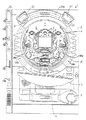
図1に示すように、パチンコ遊技機1は、額縁状に形成されたガラス扉枠2を有する。ガラス扉枠2の下部表面には打球供給皿3がある。打球供給皿3の下部には、打球供給皿3からあふれた貯留球を貯留する余剰球受皿4と打球を発射する打球操作ハンドル(操作ノブ)5が設けられている。ガラス扉枠2の後方には、遊技盤6が着脱可能に取り付けられている。また、遊技盤6の前面には遊技領域7が設けられている。
【0021】
遊技領域7の中央付近には、複数種類の図柄を可変表示するための可変表示部9と7セグメントLEDによる可変表示器10とを含む可変表示装置8が設けられている。また、可変表示器10の下部には、4個のLEDからなる通過記憶表示器(普通図柄用記憶表示器)41が設けられている。この実施の形態では、可変表示部9には、「左」、「中」、「右」の3つの図柄表示エリアがある。可変表示装置8の側部には、打球を導く通過ゲート11が設けられている。通過ゲート11を通過した打球は、球出口13を経て始動入賞口14の方に導かれる。通過ゲート11と球出口13との間の通路には、通過ゲート11を通過した打球を検出するゲートスイッチ12がある。また、始動入賞口14に入った入賞球は、遊技盤6の背面に導かれ、始動口スイッチ17によって検出される。また、始動入賞口14の下部には開閉動作を行う可変入賞球装置15が設けられている。可変入賞球装置15は、ソレノイド16によって開状態とされる。
【0022】
可変入賞球装置15の下部には、特定遊技状態(大当り状態)においてソレノイド21によって開状態とされる開閉板20が設けられている。この実施の形態では、開閉板20が大入賞口を開閉する手段となる。開閉板20から遊技盤6の背面に導かれた入賞球のうち一方(Vゾーン)に入った入賞球はVカウントスイッチ22で検出される。また、開閉板20からの入賞球はカウントスイッチ23で検出される。可変表示装置8の下部には、始動入賞口14に入った入賞球数を表示する4個の表示部を有する始動入賞記憶表示器18が設けられている。この例では、4個を上限として、始動入賞がある毎に、始動入賞記憶表示器18は点灯している表示部を1つずつ増やす。そして、可変表示部9の可変表示が開始される毎に、点灯している表示部を1つ減らす。
【0023】
遊技盤6には、複数の入賞口19,24が設けられ、遊技球の入賞口19,24への入賞は入賞口スイッチ19a,24aによって検出される。遊技領域7の左右周辺には、遊技中に点滅表示される装飾ランプ25が設けられ、下部には、入賞しなかった打球を吸収するアウト口26がある。また、遊技領域7の外側の左右上部には、効果音を発する2つのスピーカ27が設けられている。遊技領域7の外周には、遊技効果LED28aおよび遊技効果ランプ28b,28cが設けられている。
【0024】
そして、この例では、一方のスピーカ27の近傍に、景品球払出時に点灯する賞球ランプ51が設けられ、他方のスピーカ27の近傍に、補給球が切れたときに点灯する球切れランプ52が設けられている。さらに、図1には、パチンコ遊技台1に隣接して設置され、プリペイドカードが挿入されることによって球貸しを可能にするカードユニット50も示されている。
【0025】
カードユニット50には、使用可能状態であるか否かを示す使用可表示ランプ151、カード内に記録された残額情報に端数(100円未満の数)が存在する場合にその端数を打球供給皿3の近傍に設けられる度数表示LEDに表示させるための端数表示スイッチ152、カードユニット50がいずれの側のパチンコ遊技機1に対応しているのかを示す連結台方向表示器153、カードユニット50内にカードが投入されていることを示すカード投入表示ランプ154、記録媒体としてのカードが挿入されるカード挿入口155、およびカード挿入口155の裏面に設けられているカードリーダライタの機構を点検する場合にカードユニット50を解放するためのカードユニット錠156が設けられている。
【0026】
打球発射装置から発射された打球は、打球レールを通って遊技領域7に入り、その後、遊技領域7を下りてくる。打球が通過ゲート11を通ってゲートスイッチ12で検出されると、可変表示器10の表示数字が連続的に変化する状態になる。また、打球が始動入賞口14に入り始動口スイッチ17で検出されると、図柄の変動を開始できる状態であれば、可変表示部9内の図柄が回転を始める。図柄の変動を開始できる状態でなければ、始動入賞記憶を1増やす。
【0027】
可変表示部9内の画像の回転は、一定時間が経過したときに停止する。停止時の画像の組み合わせが大当り図柄の組み合わせであると、大当り遊技状態に移行する。すなわち、開閉板20が、一定時間経過するまで、または、所定個数(例えば10個)の打球が入賞するまで開放する。そして、開閉板20の開放中に打球が特定入賞領域に入賞しVカウントスイッチ22で検出されると、継続権が発生し開閉板20の開放が再度行われる。継続権の発生は、所定回数(例えば15ラウンド)許容される。
【0028】
停止時の可変表示部9内の画像の組み合わせが確率変動を伴う大当り図柄の組み合わせである場合には、次に大当りとなる確率が高くなる。すなわち、高確率状態という遊技者にとってさらに有利な状態となる。また、可変表示器10における停止図柄が所定の図柄(当り図柄)である場合に、可変入賞球装置15が所定時間だけ開状態になる。さらに、高確率状態では、可変表示器10における停止図柄が当り図柄になる確率が高められるとともに、可変入賞球装置15の開放時間と開放回数が高められる。
【0029】
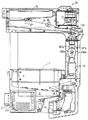
次に、パチンコ遊技機1の裏面の構造について図2を参照して説明する。
可変表示装置8の背面では、図2に示すように、機構板36の上部に遊技球タンク38が設けられ、パチンコ遊技機1が遊技機設置島に設置された状態でその上方から遊技球が遊技球タンク38に供給される。遊技球タンク38内の遊技球は、誘導樋39を通って球払出装置97に至る。
【0030】
機構板36には、中継基板30を介して可変表示部9を制御する可変表示制御ユニット29、基板ケース32に覆われ遊技制御用マイクロコンピュータ等が搭載された遊技制御基板(主基板)31、可変表示制御ユニット29と遊技制御基板31との間の信号を中継するための中継基板33、および景品球などの払出制御を行う払出制御用マイクロコンピュータなどが搭載された払出制御基板37が設置されている。さらに、機構板36の下部には、モータの回転力を利用して打球を遊技領域7に発射する打球発射装置34と、遊技効果ランプ・LED28a,28b,28c、賞球ランプ51および球切れランプ52に信号を送るためのランプ制御基板35が設置されている。
【0031】
また、図3はパチンコ遊技機1の機構板を背面からみた背面図である。誘導樋39を通った遊技球は、図3に示されるように、球切れ検出器187a,187bを通過して球供給樋186a,186bを経て球払出装置97に至る。球払出装置97から払い出された遊技球は、連絡口45を通ってパチンコ遊技機1の前面に設けられている打球供給皿3に供給される。連絡口45の側方には、パチンコ遊技機1の前面に設けられている余剰球受皿4に連通する余剰球通路46が形成されている。入賞にもとづく景品球が多数払い出されて打球供給皿3が満杯になり、ついには遊技球が連絡口45に到達した後さらに遊技球が払い出されると、遊技球は、余剰球通路46を経て余剰球受皿4に導かれる。さらに遊技球が払い出されると、感知レバー47が満タンスイッチ48を押圧して満タンスイッチ48がオンする。その状態では、球払出装置97内のステッピングモータの回転が停止して球払出装置97の動作が停止するとともに、必要に応じて打球発射装置34の駆動も停止する。なお、この実施の形態では、電気的駆動源の駆動によって遊技球を払い出す球払出装置として、ステッピングモータの回転によって遊技球が払い出される球払出装置97を例示するが、その他の駆動源によって遊技球を送り出す構造の球払出装置を用いてもよいし、電気的駆動源の駆動によってストッパを外し遊技球の自重によって払い出しがなされる構造の球払出装置を用いてもよい。
【0032】
賞球払出制御を行うために、入賞口スイッチ19a,24a、始動口スイッチ17およびVカウントスイッチ22からの信号が、主基板31に送られる。主基板31のCPU56は、始動口スイッチ17がオンすると6個の賞球払出に対応した入賞が発生したことを知る。また、カウントスイッチ23がオンすると15個の賞球払出に対応した入賞が発生したことを知る。そして、入賞口スイッチがオンすると10個の賞球払出に対応した入賞が発生したことを知る。なお、この実施の形態では、例えば、入賞口24に入賞した遊技球は、入賞口24からの入賞球流路に設けられている入賞口スイッチ24aで検出され、入賞口19に入賞した遊技球は、入賞口19からの入賞球流路に設けられている入賞口スイッチ19aで検出される。
【0033】
図4は、主基板31における回路構成の一例を示すブロック図である。なお、図4には、払出制御基板37、ランプ制御基板35、音制御基板70、発射制御基板91および表示制御基板80も示されている。主基板31には、プログラムに従ってパチンコ遊技機1を制御する基本回路53と、ゲートスイッチ12、始動口スイッチ17、Vカウントスイッチ22、カウントスイッチ23および入賞口スイッチ19a,24aからの信号を基本回路53に与えるスイッチ回路58と、可変入賞球装置15を開閉するソレノイド16および開閉板20を開閉するソレノイド21を基本回路53からの指令に従って駆動するソレノイド回路59とが搭載されている。
【0034】
また、基本回路53から与えられるデータに従って、大当りの発生を示す大当り情報、可変表示部9の画像表示開始に利用された始動入賞球の個数を示す有効始動情報、確率変動が生じたことを示す確変情報等をホール管理コンピュータ等のホストコンピュータに対して出力する情報出力回路64を含む。
【0035】
基本回路53は、ゲーム制御用のプログラム等を記憶するROM54、ワークメモリとして使用される記憶手段の一例であるRAM55、制御用のプログラムに従って制御動作を行うCPU56およびI/Oポート部57を含む。この実施の形態では、ROM54,RAM55はCPU56に内蔵されている。すなわち、CPU56は、1チップマイクロコンピュータである。なお、1チップマイクロコンピュータは、少なくともRAM55が内蔵されていればよく、ROM54およびI/Oポート部57は外付けであっても内蔵されていてもよい。また、I/Oポート部57は、マイクロコンピュータにおける情報入出力可能な端子である。
【0036】
さらに、主基板31には、電源投入時に基本回路53をリセットするためのシステムリセット回路65と、基本回路53から与えられるアドレス信号をデコードしてI/Oポート部57のうちのいずれかのI/Oポートを選択するための信号を出力するアドレスデコード回路67とが設けられている。なお、球払出装置97から主基板31に入力されるスイッチ情報もあるが、図4ではそれらは省略されている。
【0037】
遊技球を打撃して発射する打球発射装置は発射制御基板91上の回路によって制御される駆動モータ94で駆動される。そして、駆動モータ94の駆動力は、操作ノブ5の操作量に従って調整される。すなわち、発射制御基板91上の回路によって、操作ノブ5の操作量に応じた速度で打球が発射されるように制御される。
【0038】
なお、この実施の形態では、ランプ制御基板35に搭載されているランプ制御手段が、遊技盤に設けられている始動記憶表示器18、ゲート通過記憶表示器41および装飾ランプ25の表示制御を行うとともに、枠側に設けられている遊技効果ランプ・LED28a,28b,28c、賞球ランプ51および球切れランプ52の表示制御を行う。ここで、ランプ制御手段は発光体制御手段の一例である。また、特別図柄を可変表示する可変表示部9および普通図柄を可変表示する可変表示器10の表示制御は、表示制御手段(表示制御基板80)によって行われる。
【0039】
図5は、払出制御基板37および球払出装置97の構成要素などの払出に関連する構成要素を示すブロック図である。図5に示すように、満タンスイッチ48からの検出信号は、中継基板71を介して主基板31のI/Oポート57に入力される。満タンスイッチ48は、余剰球受皿4の満タンを検出するスイッチである。
【0040】
球切れスイッチ187(187a,187b)からの検出信号は、中継基板72および中継基板71を介して主基板31のI/Oポート57に入力される。球切れ検出スイッチ167は遊技球タンク38内の補給球の不足を検出するスイッチであり、球切れスイッチ187は、遊技球通路内の遊技球の有無を検出するスイッチである。
【0041】
主基板31のCPU56は、球切れスイッチ187からの検出信号が球切れ状態を示しているか、または、満タンスイッチ48からの検出信号が満タン状態を示していると、球貸し禁止を指示する払出制御コマンドを送出する。球貸し禁止を指示する払出制御コマンドを受信すると、払出制御基板37の払出制御用CPU371は、球貸し処理を停止する。
【0042】
さらに、賞球カウントスイッチ301Aからの検出信号も、中継基板72および中継基板71を介して主基板31のI/Oポート57に入力される。また、賞球カウントスイッチ301Aおよび球貸しカウントスイッチ301Bは、球払出装置97の払出機構部分に設けられ、実際に払い出された払出球を検出する。
【0043】
入賞があると、払出制御基板37には、主基板31の出力ポート(ポートG,H)577,578から賞球個数を示す払出制御コマンドが入力される。出力ポート577は8ビットのデータを出力し、出力ポート578は1ビットのストローブ信号(INT信号)を出力する。賞球個数を示す払出制御コマンドは、入力バッファ回路373を介してI/Oポート372aに入力される。払出制御用CPU371は、I/Oポート372aを介して払出制御コマンドを入力し、払出制御コマンドに応じて球払出装置97を駆動して賞球払出を行う。
なお、この実施の形態では、払出制御用CPU371は、1チップマイクロコンピュータであり、少なくともRAMが内蔵されている。
【0044】
払出制御用CPU371は、出力ポート372gを介して、貸し球数を示す球貸し個数信号をターミナル基板160に出力し、ブザー駆動信号をブザー基板75に出力する。ブザー基板75にはブザーが搭載されている。さらに、出力ポート372eを介して、エラー表示用LED374にエラー信号を出力する。
【0045】
さらに、払出制御基板37の入力ポート372bには、中継基板72を介して、賞球カウントスイッチ301Aおよび球貸しカウントスイッチ301Bからの検出信号が入力される。払出制御基板37からの払出モータ289への駆動信号は、出力ポート372cおよび中継基板72を介して球払出装置97の払出機構部分における払出モータ289に伝えられる。
【0046】
カードユニット50には、カードユニット制御用マイクロコンピュータが搭載されている。また、カードユニット50には、端数表示スイッチ152、連結台方向表示器153、カード投入表示ランプ154およびカード挿入口155が設けられている(図1参照)。残高表示基板74には、打球供給皿3の近傍に設けられている度数表示LED、球貸しスイッチおよび返却スイッチが接続される。
【0047】
残高表示基板74からカードユニット50には、遊技者の操作に応じて、球貸しスイッチ信号および返却スイッチ信号が払出制御基板37を介して与えられる。また、カードユニット50から残高表示基板74には、プリペイドカードの残高を示すカード残高表示信号および球貸し可表示信号が払出制御基板37を介して与えられる。カードユニット50と払出制御基板37の間では、接続信号(VL信号)、ユニット操作信号(BRDY信号)、球貸し要求信号(BRQ信号)、球貸し完了信号(EXS信号)およびパチンコ機動作信号(PRDY信号)がI/Oポート372fを介してやりとりされる。
【0048】
パチンコ遊技機1の電源が投入されると、払出制御基板37の払出制御用CPU371は、カードユニット50にPRDY信号を出力する。また、カードユニット制御用マイクロコンピュータは、VL信号を出力する。払出制御用CPU371は、VL信号の入力状態により接続状態/未接続状態を判定する。カードユニット50においてカードが受け付けられ、球貸しスイッチが操作され球貸しスイッチ信号が入力されると、カードユニット制御用マイクロコンピュータは、払出制御基板37にBRDY信号を出力する。この時点から所定の遅延時間が経過すると、カードユニット制御用マイクロコンピュータは、払出制御基板37にBRQ信号を出力する。そして、払出制御基板37の払出制御用CPU371は、カードユニット50に対するEXS信号を立ち上げ、カードユニット50からのBRQ信号の立ち下がりを検出すると、払出モータ289を駆動し、所定個の貸し球を遊技者に払い出す。このとき、振分用ソレノイド310は駆動状態とされている。すなわち、球振分部材311を球貸し側に向ける。そして、払出が完了したら、払出制御用CPU371は、カードユニット50に対するEXS信号を立ち下げる。その後、カードユニット50からのBRDY信号がオン状態でなければ、賞球払出制御を実行する。
【0049】
以上のように、カードユニット50からの信号は全て払出制御基板37に入力される構成になっている。従って、球貸し制御に関して、カードユニット50から主基板31に信号が入力されることはなく、主基板31の基本回路53にカードユニット50の側から不正に信号が入力される余地はない。なお、主基板31および払出制御基板37には、ソレノイドおよびモータやランプを駆動するためのドライバ回路が搭載されているが、図5では、それらの回路は省略されている。
【0050】
なお、この実施の形態ではカードユニット50が設けられている場合を例にするが、コイン投入に応じてその金額に応じた遊技球を貸し出す場合にも本発明を適用できる。また、この実施の形態では遊技球を貸し出す場合を例にしているが、得点が加算されるものであっても本発明を適用できる。
【0051】
この実施の形態では、主基板31および払出制御基板37におけるRAMは、バックアップ電源でバックアップされている。すなわち、遊技機に対する電力供給が停止しても、所定期間はRAMの内容が保存される。そして、各CPUは、電源電圧の低下を検出すると、所定の処理を行った後に電源復旧待ちの状態になる。また、電源投入時に、各CPUは、RAMにデータが保存されている場合には、保存データにもとづいて電源断前の状態を復元する。
【0052】
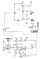
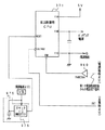
図6は、電源監視および電源バックアップのためのCPU56周りの一構成例を示すブロック図である。図6に示すように、第1の電源監視回路(電源監視手段、または第1の電源監視手段)からの電圧低下信号が、CPU56のマスク不能割込端子(NMI端子)に接続されている。第1の電源監視回路は、遊技機が使用する各種直流電源のうちのいずれかの電源の電圧を監視して電源電圧低下を検出する回路である。この実施の形態では、VSLの電源電圧を監視して電圧値が所定値以下になるとローレベルの電圧低下信号を発生する。VSLは、遊技機で使用される直流電圧のうちで最大のものであり、この例では+30Vである。従って、CPU56は、割込処理によって電源断の発生を確認することができる。なお、この実施の形態では、第1の電源監視回路は、後述する電源基板に搭載されている。
【0053】
図6には、システムリセット回路65も示されているが、この実施の形態では、システムリセット回路65は、第2の電源監視回路(第2の電源監視手段)も兼ねている。すなわち、リセットIC651は、電源投入時に、外付けのコンデンサの容量で決まる所定時間だけ出力をローレベルとし、所定時間が経過すると出力をハイレベルにする。すなわち、リセット信号をハイレベルに立ち上げてCPU56を動作可能状態にする。また、リセットIC651は、第1の電源監視回路が監視する電源電圧と等しい電源電圧であるVSLの電源電圧を監視して電圧値が所定値(第1の電源監視回路が電圧低下信号を出力する電源電圧値よりも低い値)以下になるとローレベルの電圧低下信号を発生する。従って、CPU56は、第1の電源監視回路からの電圧低下信号に応じて所定の電力供給停止時処理を行った後、システムリセットされる。なお、この実施の形態では、リセット信号と第2の電源監視回路からの電圧低下信号とは同一の信号である。
【0054】
図6に示すように、リセットIC651からのリセット信号は、NAND回路947に入力されるとともに、反転回路(NOT回路)944を介してカウンタIC941のクリア端子に入力される。カウンタIC941は、クリア端子への入力がローレベルになると、発振器943からのクロック信号をカウントする。そして、カウンタIC941のQ5出力がNOT回路945,946を介してNAND回路947に入力される。また、カウンタIC941のQ6出力は、フリップフロップ(FF)942のクロック端子に入力される。フリップフロップ942のD入力はハイレベルに固定され、Q出力は論理和回路(OR回路)949に入力される。OR回路949の他方の入力には、NAND回路947の出力がNOT回路948を介して導入される。そして、OR回路949の出力がCPU56のリセット端子に接続されている。このような構成によれば、電源投入時に、CPU56のリセット端子に2回のリセット信号(ローレベル信号)が与えられるので、CPU56は、確実に動作を開始する。
【0055】
そして、例えば、第1の電源監視回路の検出電圧(電圧低下信号を出力することになる電圧)を+22Vとし、第2の電源監視回路の検出電圧を+9Vとする。そのように構成した場合には、第1の電源監視回路と第2の電源監視回路とは、同一の電源VSLの電圧を監視するので、第1の電圧監視回路が電圧低下信号を出力するタイミングと第2の電圧監視回路が電圧低下信号を出力するタイミングの差を所望の所定期間に確実に設定することができる。所望の所定期間とは、第1の電源監視回路からの電圧低下信号に応じて電力供給停止時処理を開始してから電力供給停止時処理が確実に完了するまでの期間である。
【0056】
この例では、第1の電源監視手段が検出信号を出力することになる第1検出条件は+30V電源電圧が+22Vにまで低下したことであり、第2の電源監視手段が検出信号を出力することになる第2検出条件は+30V電源電圧が+9Vにまで低下したことになる。ただし、ここで用いられている電圧値は一例であって、他の値を用いてもよい。
【0057】
ただし、監視範囲が狭まるが、第1の電圧監視回路および第2の電圧監視回路の監視電圧として+5V電源電圧を用いることも可能である。その場合にも、第1の電圧監視回路の検出電圧は、第2の電圧監視回路の検出電圧よりも高く設定される。
【0058】
CPU56等の駆動電源である+5V電源から電力が供給されていない間、RAMの少なくとも一部は、電源基板から供給されるバックアップ電源によってバックアップされ、遊技機に対する電源が断しても内容は保存される。そして、+5V電源が復旧すると、システムリセット回路65からリセット信号が発せられるので、CPU56は、通常の動作状態に復帰する。そのとき、必要なバックアップが保存されているため、停電等からの復旧時に停電発生時の遊技状態に復帰することができる。
【0059】
なお、図6では、電源投入時にCPU56のリセット端子に2回のリセット信号(ローレベル信号)が与えられる構成が示されたが、リセット信号の立ち上がりタイミングが1回しかなくても確実にリセット解除されるCPUを使用する場合には、符号941〜949で示された回路素子は不要である。その場合、リセットIC651の出力がそのままCPU56のリセット端子に接続される。
【0060】
図7は、遊技機の電源基板910の一構成例を示すブロック図である。電源基板910は、主基板31、表示制御基板80、音声制御基板70、ランプ制御基板35および払出制御基板37等の電気部品制御基板と独立して設置され、遊技機内の各電気部品制御基板および機構部品が使用する電圧を生成する。この例では、AC24V、VSL(DC+30V)、DC+21V、DC+12VおよびDC+5Vを生成する。また、バックアップ電源となるコンデンサ916は、DC+5Vすなわち各基板上のIC等を駆動する電源のラインから充電される。
【0061】
トランス911は、交流電源からの交流電圧を24Vに変換する。AC24V電圧は、コネクタ915に出力される。また、整流回路912は、AC24Vから+30Vの直流電圧を生成し、DC−DCコンバータ913およびコネクタ915に出力する。DC−DCコンバータ913は、+22V、+12Vおよび+5Vを生成してコネクタ915に出力する。コネクタ915は例えば中継基板に接続され、中継基板から各電気部品制御基板および機構部品に必要な電圧の電力が供給される。なお、トランス911の入力側には、遊技機に対する電源供給を停止したり開始させたりするための電源スイッチ918が設置されている。
【0062】
DC−DCコンバータ913からの+5Vラインは分岐してバックアップ+5Vラインを形成する。バックアップ+5Vラインとグラウンドレベルとの間には大容量のコンデンサ916が接続されている。コンデンサ916は、遊技機に対する電力供給が遮断されたときの電気部品制御基板のバックアップRAM(電源バックアップされているRAMすなわち記憶内容保持状態となりうる記憶手段)に対して記憶状態を保持できるように電力を供給するバックアップ電源となる。また、+5Vラインとバックアップ+5Vラインとの間に、逆流防止用のダイオード917が挿入される。
【0063】
なお、バックアップ電源として、+5V電源から充電可能な電池を用いてもよい。電池を用いる場合には、+5V電源から電力供給されない状態が所定時間継続すると容量がなくなるような充電池が用いられる。
【0064】
また、電源基板910には、上述した第1の電源監視回路を構成する電源監視用IC902が搭載されている。電源監視用IC902は、VSL電源電圧を導入し、VSL電源電圧を監視することによって電源断の発生を検出する。具体的には、VSL電源電圧が所定値(この例では+22V)以下になったら、電源断が生ずるとして電圧低下信号を出力する。なお、監視対象の電源電圧は、各電気部品制御基板に搭載されている回路素子の電源電圧(この例では+5V)よりも高い電圧であることが好ましい。この例では、交流から直流に変換された直後の電圧であるVSLが用いられている。電源監視用IC902からの電圧低下信号は、主基板31や払出制御基板37等に供給される。
【0065】
電源監視用IC902が電源断を検知するための所定値は、通常時の電圧より低いが、各電気部品制御基板上のCPUが暫くの間動作しうる程度の電圧である。また、電源監視用IC902が、CPU等の回路素子を駆動するための電圧(この例では+5V)よりも高く、また、交流から直流に変換された直後の電圧を監視するように構成されているので、CPUが必要とする電圧に対して監視範囲を広げることができる。従って、より精密な監視を行うことができる。さらに、監視電圧としてVSL(+30V)を用いる場合には、遊技機の各種スイッチに供給される電圧が+12Vであることから、電源瞬断時のスイッチオン誤検出の防止も期待できる。すなわち、+30V電源の電圧を監視すると、+30V作成の以降に作られる+12Vが落ち始める以前の段階でそれの低下を検出できる。よって、+12V電源の電圧が低下するとスイッチ出力がオン状態を呈するようになるが、+12Vより早く低下する+30V電源電圧を監視して電源断を認識すれば、スイッチ出力がオン状態を呈する前に電源復旧待ちの状態に入ってスイッチ出力を検出しない状態となることができる。
【0066】
また、電源監視用IC902は、電気部品制御基板とは別個の電源基板910に搭載されているので、第1の電源監視回路から複数の電気部品制御基板に電圧低下信号を供給することができる。電圧低下信号を必要とする電気部品制御基板が幾つあっても第1の電源監視手段は1つ設けられていればよいので、各電気部品制御基板における各電気部品制御手段が後述する復帰制御を行っても、遊技機のコストはさほど上昇しない。
【0067】
なお、図7に示された構成では、電源監視用IC902の検出出力(電圧低下信号)は、バッファ回路918,919を介してそれぞれの電気部品制御基板(例えば主基板31と払出制御基板37)に伝達されるが、例えば、1つの検出出力を中継基板に伝達し、中継基板から各電気部品制御基板に同じ信号を分配する構成でもよい。また、電圧低下信号を必要とする基板数に応じたバッファ回路を設けてもよい。
【0068】
次に遊技機の動作について説明する。
図8は、主基板31におけるCPU56が実行するメイン処理を示すフローチャートである。遊技機に対する電源が投入されると、メイン処理において、CPU56は、まず、必要な初期設定を行う(ステップS1)。
【0069】
そして、電源断時にバックアップRAM領域のデータ保護処理(本例ではパリティデータの付加等の停電発生NMI処理)が行われたか否かの確認を行う(ステップS2)。不測の電源断が生じた場合には、後述するようにバックアップRAM領域のデータを保護するための処理が行われている。そのような保護処理が行われていた場合をバックアップありとする。バックアップなしという確認結果であれば、初期化処理を実行する(ステップS2,S3)。なお、本例では、バックアップRAM領域にバックアップデータがあるか否かは、電源断時にバックアップRAM領域に設定されるバックアップフラグの状態によって確認する。本例では、バックアップフラグ領域に「55H」が設定されていればバックアップあり(オン状態)を意味し、「55H」以外の値が設定されていればバックアップなし(オフ状態)を意味する。
【0070】
バックアップRAM領域にバックアップデータがある場合には、この実施の形態では、CPU56は、バックアップRAM領域のデータチェック(この例ではパリティチェック)を行う(ステップS4)。不測の電源断が生じた後に復旧した場合には、バックアップRAM領域のデータは保存されていたはずであるから、チェック結果は正常になる。チェック結果が正常でない場合には、内部状態を電源断時の状態に戻すことができないので、停電復旧時でない電源投入時に実行される初期化処理を実行する(ステップS5,S3)。
【0071】
チェック結果が正常であれば、CPU56は、内部状態を電源断時の状態に戻すための遊技状態復旧処理を行う(ステップS6)。従って、本例では、図9に示すように、バックアップフラグの値が「55H」に設定されており、かつチェック結果が正常である場合に、ステップS6の遊技状態復旧処理に移行する。そして、バックアップRAM領域に保存されていたPC(プログラムカウンタ)の指すアドレスに復帰する(ステップS7)。
【0072】
通常の初期化処理の実行(ステップS2,S3)を終えると、CPU56により実行されるメイン処理は、タイマ割込フラグの監視(ステップS9)の確認が行われるループ処理に移行する。なお、ループ内では、表示用乱数更新処理(ステップS8)も実行される。
【0073】
なお、この実施の形態では、ステップS2でバックアップデータの有無を確認したあと、バックアップデータが存在する場合にステップS4でバックアップ領域のチェックを行うようにしていたが、逆に、バックアップ領域のチェック結果が正常であったことを確認したあと、バックアップデータの有無の確認を行うようにしてもよい。また、バックアップデータの有無の確認、またはバックアップ領域のチェックの何れか一方の確認を行うことで、停電復旧処理を実行するか否かを判定する構成としてもよい。
【0074】
また、例えば停電復旧処理を実行するか否か判断する場合のパリティチェック(ステップS4)の際に、すなわち、遊技状態を復旧するか否か判断する際に、保存されていたRAMデータにおける特別プロセスフラグ等や始動入賞記憶数データによって、遊技機が遊技待機状態(図柄変動中でなく、大当り遊技中でなく、確変中でなく、また、始動入賞記憶がない状態)であることが確認されたら、遊技状態復旧処理を行わずに初期化処理を実行するようにしてもよい。
【0075】
通常の初期化処理では、図10に示すように、RAMのクリア処理が行われる(ステップS3a)。次いで、作業領域初期設定テーブルのアドレス値にもとづいて、所定の作業領域(例えば、普通図柄判定用乱数カウンタ、普通図柄判定用バッファ、特別図柄左中右図柄バッファ、払出コマンド格納ポインタなど)に初期値を設定する初期値設定処理(ステップS3b)が行われる。そして、2ms毎に定期的にタイマ割込がかかるようにCPU56に設けられているタイマレジスタの初期設定(タイムアウトが2msであることと繰り返しタイマが動作する設定)が行われる(ステップS3c)。すなわち、ステップS3cで、タイマ割込を能動化する処理と、タイマ割込インタバルを設定する処理とが実行される。そして、初期設定処理(ステップS1)において割込禁止(図12参照)とされているため、初期化処理を終える前に割込が許可される(ステップS3d)。
【0076】
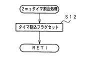
従って、この実施の形態では、CPU56の内部タイマが繰り返しタイマ割込を発生するように設定される。この実施の形態では、繰り返し周期は2msに設定される。そして、図11に示すように、タイマ割込が発生すると、CPU56は、タイマ割込フラグをセットする(ステップS12)。
【0077】
CPU56は、ステップS9において、タイマ割込フラグがセットされたことを検出すると、タイマ割込フラグをリセットするとともに(ステップS10)、遊技制御処理を実行する(ステップS11)。以上の制御によって、この実施の形態では、遊技制御処理は2ms毎に起動されることになる。なお、この実施の形態では、タイマ割込処理ではフラグセットのみがなされ、遊技制御処理はメイン処理において実行されるが、タイマ割込処理で遊技制御処理を実行してもよい。
【0078】
このように、この実施の形態では、バックアップデータの有無により電源断時の状態に復旧するか否かの判断を行うようにしている。従って、停電後の電源復旧時などにおいて電源投入された時に、バックアップデータ記憶領域の内容に応じて電源断時の状態に復旧させるか否かの判断を行うことができる。
【0079】
また、上述したように、バックアップデータの状態により電源断時の状態に復旧するか否かの判断を行うようにしているため、停電後の電源復旧時などにおいて電源投入された時に、バックアップデータ記憶領域の内容の状態に応じて電源断時の状態に復旧させるか否かの判断を行うことができる。
【0080】
図12は、ステップS1の初期設定処理を示すフローチャートである。初期設定処理において、CPU56は、まず、割込禁止に設定する(ステップS1a)。割込禁止に設定すると、CPU56は、割込モードを割込モード2に設定し(ステップS1b)、スタックポインタにスタックポインタ指定アドレスを設定する(ステップS1c)。そして、CPU56は、内蔵デバイスレジスタの初期化(ステップS1d)、CTC(カウンタ/タイマ)およびPIO(パラレル入出力ポート)の初期化(ステップS1e)を行ったあと、RAMをアクセス可能状態に設定する(ステップS1f)。
【0081】
なお、初期設定処理にて設定され得るINT信号の入力により割込が許可されるマスカブル割込の割込モードには、以下の3種類のモードがある。
割込モード0:割込要求を行った内蔵デバイスがRST命令(1バイト)またはCALL命令(3バイト)をCPUの内部データバス上に送出する。よって、CPU56は、RST命令に対応したアドレスまたはCALL命令で指定されるアドレスの命令を実行する。リセット時に、CPU56は自動的に割込モード0になる。よって、割込モード1または割込モード2に設定したい場合には、初期設定処理において、割込モード1または割込モード2に設定するための処理を行う必要がある。
割込モード1:割込処理プログラムのスタートアドレス(38(H))が、予め定められているモードである。
割込モード2:CPU56の特定レジスタの値(1バイト)と内蔵デバイスが出力する割込ベクタ(1バイト:最下位ビット0)から合成されるアドレスが、割込番地を示すモードである。すなわち、割込番地は、上位アドレスが特定レジスタの値とされ、下位アドレスが割込ベクタとされた2バイトで示されるアドレスである。
【0082】
図13は、ステップS11の遊技制御処理を示すフローチャートである。遊技制御処理において、CPU56は、まず、スイッチ回路58を介して、ゲートセンサ12、始動口センサ17、カウントセンサ23および入賞口スイッチ19a,24aの状態を入力し、各入賞口や入賞装置に対する入賞があったか否か判定する(スイッチ処理:ステップS21)。
【0083】
次いで、パチンコ遊技機1の内部に備えられている自己診断機能によって種々の異常診断処理が行われ、その結果に応じて必要ならば警報が発せられる(エラー処理:ステップS22)。
【0084】
次に、遊技制御に用いられる大当り判定用の乱数等の各判定用乱数を示す各カウンタを更新する処理を行う(ステップS23)。CPU56は、さらに、停止図柄の種類を決定する乱数等の表示用乱数を更新する処理を行う(ステップS24)。
【0085】
さらに、CPU56は、特別図柄プロセス処理を行う(ステップS25)。特別図柄プロセス制御では、遊技状態に応じてパチンコ遊技機1を所定の順序で制御するための特別図柄プロセスフラグに従って該当する処理が選び出されて実行される。そして、特別図柄プロセスフラグの値は、遊技状態に応じて各処理中に更新される。また、普通図柄プロセス処理を行う(ステップS26)。普通図柄プロセス処理では、7セグメントLEDによる可変表示器10を所定の順序で制御するための普通図柄プロセスフラグに従って該当する処理が選び出されて実行される。そして、普通図柄プロセスフラグの値は、遊技状態に応じて各処理中に更新される。
【0086】
また、CPU56は、表示制御基板80に送出される表示制御コマンド(特別図柄制御コマンドや普通図柄制御コマンド)をRAM55の所定の領域に設定する処理を行った後に、特別図柄制御コマンドや普通図柄制御コマンドを出力する処理を行う(特別図柄コマンド制御処理:ステップS27,普通図柄コマンド制御処理:ステップS28)。
【0087】
次いで、CPU56は、各種出力データの格納領域の内容を各出力ポートに出力する処理を行う(データ出力処理:ステップS29)。なお、CPU56は、例えばホール管理用コンピュータに出力される大当り情報、始動情報、確率変動情報などの出力データを格納領域に設定する出力データ設定処理などの他の処理も行う。
【0088】
また、CPU56は、所定の条件が成立したときにソレノイド回路59に駆動指令を行う(ステップS30)。ソレノイド回路59は、駆動指令に応じてソレノイド16,21を駆動し、可変入賞球装置15または開閉板20を開状態または閉状態とする。
【0089】
また、CPU56は、各入賞口17,23,19a,24aの検出に基づく賞球数の設定などを行う(ステップS31)。すなわち、所定の条件が成立すると払出制御基板37に払出制御コマンドを出力する。払出制御基板37に搭載されている払出制御用CPU371は、払出制御コマンドに応じて球払出装置97を駆動する。
【0090】
以上のように、メイン処理には遊技制御処理に移行すべきか否かを判定する処理が含まれ、CPU56の内部タイマが定期的に発生するタイマ割込にもとづくタイマ割込処理で遊技制御処理に移行すべきか否かを判定するためのフラグがセットされるので、遊技制御処理の全てが確実に実行される。つまり、遊技制御処理の全てが実行されるまでは、次回の遊技制御処理に移行すべきか否かの判定が行われないので、遊技制御処理中の全ての各処理が実行完了することは保証されている。
【0091】
従来の一般的な遊技制御処理は、定期的に発生する外部割込によって、強制的に最初の状態に戻されていた。図13に示された例に則して説明すると、例えば、ステップS31の処理中であっても、強制的にステップS21の処理に戻されていた。つまり、遊技制御処理中の全ての各処理が実行完了する前に、次回の遊技制御処理が開始されてしまう可能性があった。
【0092】
なお、ここでは、主基板31のCPU56が実行する遊技制御処理は、CPU56の内部タイマが定期的に発生するタイマ割込にもとづくタイマ割込処理でセットされるフラグに応じて実行されたが、定期的に(例えば2ms毎)信号を発生するハードウェア回路を設け、その回路からの信号をCPU56の外部割込端子に導入し、割込信号によって遊技制御処理に移行すべきか否かを判定するためのフラグをセットするようにしてもよい。
【0093】
そのように構成した場合にも、遊技制御処理の全てが実行されるまでは、フラグの判定が行われないので、遊技制御処理中の全ての各処理が実行完了することが保証される。
【0094】
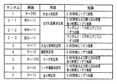
図14は、遊技制御に用いられる大当り決定用乱数等の各乱数を示す説明図である。各乱数は、以下のように使用される。
(1)ランダム1:大当りを発生させるか否か決定する(大当り決定用)
(2)ランダム2−1〜2−3:左右中のはずれ図柄決定用
(3)ランダム3:大当り時の図柄の組合せを決定する(大当り図柄決定用)
(4)ランダム4:確変大当りとするか否か決定する(確変判定用)
(5)ランダム5:はずれ時にリーチするか否か決定する(リーチ判定用)
(6)ランダム6:リーチ種類を決定する(リーチ種類決定用)
(7)ランダム7:普通図柄による当りとするか否か決定する(当り判定用)
【0095】
なお、遊技効果を高めるために、上記(1)〜(7)の乱数以外の乱数も用いられている。
ステップS23では、CPU56は、(1)の大当り決定用乱数、(3)の大当り図柄決定用乱数、(4)の確変判定用乱数および(7)の当り判定用乱数を生成するためのカウンタのカウントアップ(1加算)を行う。すなわち、それらが判定用乱数である。
【0096】
次に、始動入賞口14への入賞にもとづいて可変表示部9に可変表示される図柄(特別図柄)の決定方法について図15〜図17のフローチャートを参照して説明する。図15は打球が始動入賞口14に入賞したことを判定する処理を示し、図16は可変表示部9の可変表示の停止図柄を決定する処理を示す。図17は、大当りとするか否か決定する処理を示すフローチャートである。なお、ここでは、大当りとする場合に、確変とするか否かをも決定したあと停止図柄を決定するようにしているが、大当り停止図柄は確変大当りとは関係なく決定されるようにしても良い。この場合、確変とするか否かの判断については、大当り決定後(例えば、大当り決定直後や、大当り状態終了後など)に別個に行われるようにしてもよい。
【0097】
打球が遊技盤6に設けられている始動入賞口14に入賞すると、始動口センサ17がオンする。遊技制御処理のステップS25の特別図柄プロセス処理において、図15に示すように、CPU56は、スイッチ回路58を介して始動口センサ17がオンしたことを判定すると(ステップS71)、始動入賞記憶数が最大値である4に達しているかどうか確認する(ステップS72)。始動入賞記憶数が4に達していなければ、始動入賞記憶数を1増やし(ステップS73)、大当り決定用乱数の値を抽出する。そして、それを始動入賞記憶数の値に対応した乱数値格納エリアに格納する(ステップS74)。なお、始動入賞記憶数が4に達している場合には、始動入賞記憶数を増やす処理を行わない。すなわち、この実施の形態では、最大4個の始動入賞口17に入賞した打球数が記憶可能である。
【0098】
図16に示すように、CPU56は、ステップS25の特別図柄プロセス処理において始動入賞記憶数の値を確認する(ステップS81)。始動入賞記憶数が0でなければ、始動入賞記憶数=1に対応する乱数値格納エリアに格納されている値を読み出すとともに(ステップS82)、始動入賞記憶数の値を1減らし、かつ、各乱数値格納エリアの値をシフトする(ステップS83)。すなわち、始動入賞記憶数=n(n=2,3,4)に対応する乱数値格納エリアに格納されている値を、始動入賞記憶数=n−1に対応する乱数値格納エリアに格納する。
【0099】
そして、CPU56は、ステップS82で読み出した値、すなわち抽出されている大当り決定用乱数の値にもとづいて当たり/はずれを決定する(ステップS84)。ここでは、大当り決定用乱数は0〜299の範囲の値をとることにする。図17に示すように、低確率時には例えばその値が「3」である場合に「大当り」と決定し、それ以外の値である場合には「はずれ」と決定する。高確率時には例えばその値が「3」,「7」,「79」,「103」,「107」のいずれかである場合に「大当り」と決定し、それ以外の値である場合には「はずれ」と決定する。
【0100】
大当りと判定されたときには、CPU56は、確変判定用乱数(ランダム4)の値にもとづいて確変大当りとするか否か決定する(ステップS85)。そして、確変大当りとすることに決定された場合には(ステップS86)、確変フラグをセットする(ステップS87)。なお、確変フラグは、リーチ種類の選択等で使用される。また、大当り図柄決定用乱数(ランダム3)を抽出しその値に従って大当り図柄を決定する(ステップS88)。さらに、リーチ種類決定用乱数(ランダム6)を抽出しその値にもとづいてリーチ種類を決定する(ステップS89)。
【0101】
はずれと判定された場合には、CPU56は、リーチとするか否か判定する(ステップS90)。例えば、リーチ判定用の乱数であるランダム4の値が「105」〜「1530」のいずれかである場合には、リーチとしないと決定する。そして、リーチ判定用乱数の値が「0」〜「104」のいずれかである場合にはリーチとすることを決定する。リーチとすることを決定したときには、CPU56は、リーチ図柄の決定を行う。
【0102】
この実施の形態では、ランダム2−1の値に従って左右図柄を決定する(ステップS91)。また、ランダム2−2の値に従って中図柄を決定する(ステップS92)。すなわち、ランダム2−1およびランダム2−2の値の0〜15の値に対応したいずれかの図柄が停止図柄として決定される。ここで、決定された中図柄が左右図柄と一致した場合には、中図柄に対応した乱数の値に1加算した値に対応する図柄を中図柄の確定図柄として、大当り図柄と一致しないようにする。
【0103】
さらに、CPU56は、リーチ種類決定用乱数(ランダム6)を抽出しその値にもとづいてリーチ種類を決定する(ステップS89)。ステップS90において、リーチしないことに決定された場合には、ランダム2−1〜2−3の値に応じて左右中図柄を決定する(ステップS93)。
【0104】
以上のようにして、始動入賞にもとづく図柄変動の表示態様を大当りとするか、リーチ態様とするか、はずれとするか決定され、それぞれの停止図柄の組合せが決定される。
【0105】
なお、高確率状態において、次に大当りとなる確率が上昇するとともに、7セグメントLEDによる可変表示器10の可変表示の確定までの時間が短縮され、かつ、可変表示器10の可変表示結果にもとづく当たり時の可変入賞球装置15の開放回数および開放時間が高められるようにパチンコ遊技機1が構成されていてもよいし、可変表示器10の可変表示結果にもとづく当たりの確率が高くなるように構成されていてもよい。また、それらのうちのいずれか一つまたは複数の状態のみが生ずるパチンコ遊技機1であってもよい。
【0106】
また、この実施の形態で用いられた乱数および乱数値の範囲は一例であって、どのような乱数を用いてもよいし、範囲設定も任意である。
【0107】
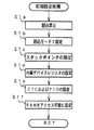
図18は、CPU56が実行する特別図柄プロセス処理のプログラムの一例を示すフローチャートである。図18に示す特別図柄プロセス処理は、図13のフローチャートにおけるステップS25の具体的な処理である。CPU56は、特別図柄プロセス処理を行う際に、変動短縮タイマ減算処理(ステップS310)を行ったあと、その内部状態に応じて、図18に示すステップS300〜S309のうちのいずれかの処理を行う。
【0108】
ステップS310の変動短縮タイマ減算処理では、特別図柄の変動時間短縮の条件を満たしているか否か(例えば、始動入賞検出時から、その始動入賞にもとづく処理が実行されるまでに所定時間が経過しているか否か)を確認するための変動短縮タイマを減算する処理が行われる。そして、ステップS300〜S309の各処理において、以下のような処理が実行される。
【0109】
特別図柄変動待ち処理(ステップS300):始動入賞口14(この実施の形態では可変入賞球装置15の入賞口)に打球入賞して始動口センサ17がオンするのを待つ。始動口センサ17がオンすると、始動入賞記憶数が満タンでなければ、始動入賞記憶数を+1するとともに大当り決定用乱数を抽出する。すなわち、図15に示された処理が実行される。
特別図柄判定処理(ステップS301):特別図柄の可変表示が開始できる状態になると、始動入賞記憶数を確認する。始動入賞記憶数が0でなければ、抽出されている大当り決定用乱数の値に応じて大当りとするかはずれとするか決定する。すなわち、図16に示された処理の前半が実行される。
停止図柄設定処理(ステップS302):左右中図柄の停止図柄を決定する。すなわち、図16に示された処理の中半が実行される。
【0110】
リーチ動作設定処理(ステップS303):リーチ判定用乱数の値に応じてリーチ動作するか否か決定するとともに、リーチ種類決定用乱数の値に応じてリーチ時の変動期間を決定する。すなわち、図16に示された処理の後半が実行される。
【0111】
全図柄変動開始処理(ステップS304):可変表示部9において全図柄が変動開始されるように制御する。このとき、表示制御基板80に対して、左右中最終停止図柄と変動態様を指令する情報とが送信される。処理を終えると、内部状態(プロセスフラグ)をステップS305に移行するように更新する。
【0112】
全図柄停止待ち処理(ステップS305):所定時間(ステップS310の変動短縮タイマで示された時間)が経過すると、可変表示部9において表示される全図柄が停止されるように制御する。そして、停止図柄が大当り図柄の組み合わせである場合には、内部状態(プロセスフラグ)をステップS306に移行するように更新する。そうでない場合には、内部状態をステップS300に移行するように更新する。
【0113】
大入賞口開放開始処理(ステップS306):大入賞口を開放する制御を開始する。具体的には、カウンタやフラグを初期化するとともに、ソレノイド21を駆動して大入賞口を開放する。また、大当りフラグ(大当り中であることを示すフラグ)のセットを行う。処理を終えると、内部状態(プロセスフラグ)をステップS307に移行するように更新する。
【0114】
大入賞口開放中処理(ステップS307):大入賞口ラウンド表示の表示制御コマンドデータを表示制御基板80に送出する制御や大入賞口の閉成条件の成立を確認する処理等を行う。最終的な大入賞口の閉成条件が成立したら、内部状態をステップS308に移行するように更新する。
【0115】
特定領域有効時間処理(ステップS308):Vカウントスイッチ22の通過の有無を監視して、大当り遊技状態継続条件の成立を確認する処理を行う。大当り遊技状態継続の条件が成立し、かつ、まだ残りラウンドがある場合には、内部状態をステップS306に移行するように更新する。また、所定の有効時間内に大当り遊技状態継続条件が成立しなかった場合、または、全てのラウンドを終えた場合には、内部状態をステップS309に移行するように更新する。
【0116】
大当り終了処理(ステップS309):大当り遊技状態が終了したことを遊技者に報知するための表示を行う。その表示が終了したら、内部状態をステップS300に移行するように更新する。
【0117】
上述したように、始動入賞口14に打球が入賞すると、基本回路53は、ステップS25(図13参照)の特別図柄プロセス処理において、大当りとするかはずれとするか、停止図柄、リーチ態様、確変とするかしないかを決定するが、その決定に応じた表示制御コマンドなどの制御コマンドを、表示制御手段などの電気部品制御手段に送出する。例えば表示制御手段では、主基板31からの表示制御コマンドに応じて可変表示部9の表示制御が行われる。
【0118】
図19は、普通図柄プロセス処理(ステップS26)を示すフローチャートである。普通図柄プロセス処理では、CPU56は、ステップS61のゲートスイッチ処理を実行した後に、普通図柄プロセスフラグの値に応じてステップS62〜S66に示された処理のうちのいずれかの処理を実行する。
【0119】
図20に示すように、ゲートスイッチ処理では、普通図柄変動開始の条件となる通過ゲート11の打球通過にもとづくゲートスイッチ12のオンを検出する(ステップS611)。ゲートスイッチ12がオンしていたら、ゲート通過記憶カウンタが最大値(この例では「4」)に達しているか否か確認する(ステップS612)。達していなければ、ゲート通過記憶カウンタの値を+1する(ステップS613)。なお、ゲート通過記憶カウンタの値に応じて通過記憶表示器41のLEDが点灯される。そして、CPU56は、当り判定用乱数(ランダム7)の値を抽出し、その値を記憶する(S614)。
【0120】
ステップS62の普通図柄変動待ち処理では、CPU56は、普通図柄通過記憶カウンタの値が0以外であれば、普通図柄プロセスフラグの値を更新する。普通図柄通過記憶カウンタの値が0であれば何もしない。
【0121】
図21は、この実施の形態での当り判定用乱数(ランダム7)と当り/はずれとの関係を示す説明図である。図21に示すように、高確率のときには当り値は3〜12のいずれかであり、低確率のときには3、5または7である。当り判定用乱数の値が当り値と一致すれば、当りと決定される。なお、普通図柄の高確率時は、例えば確変時と一致する。
【0122】
図22は、ステップS63の普通図柄判定処理を示すフローチャートである。普通図柄判定処理では、CPU56は、ゲート通過記憶数=1に対応する乱数値格納エリアに格納されている値を読み出すとともに(ステップS631)、ゲート通過記憶カウンタの値を1減らし、かつ、各乱数値格納エリアの値をシフトする(ステップS632)。すなわち、ゲート通過記憶カウンタ=n(n=2,3,4)に対応する乱数値格納エリアに格納されている値を、ゲート通過記憶カウンタ=n−1に対応する乱数値格納エリアに格納する。
【0123】
そして、CPU56は、ステップS631で読み出した値、すなわち抽出されている当り判定用乱数の値にもとづいて当たり/はずれを決定する(ステップS633)。すなわち、図21に示された関係にもとづいて当たり/はずれを決定する。そして、所定の乱数等にもとづいて普通図柄の停止図柄を決定する(ステップS634)。例えば、普通図柄が0〜9の数字であり、当り図柄が「3」,「7」であるとすると、当りとする場合には停止図柄を「3」または「7」に決定し、はずれの場合には「3」,「7」以外の値に決定する。
【0124】
また、普通図柄の停止図柄を表示制御基板80に通知するために、停止図柄を示す表示制御コマンドを送信するための制御を行う(ステップS635)。具体的には、所定の格納領域(RAM)に停止図柄を示す表示制御コマンドを格納し、コマンド送出要求のフラグをセットする。そのフラグは、遊技制御処理におけるデータ出力処理(ステップS29)で参照される。次いで、普通図柄変動開始を示す表示制御コマンドを送信するための制御を行う(ステップS636)。具体的には、所定の格納領域(RAM)に普通図柄変動開始を示す表示制御コマンドを格納し、コマンド送出要求のフラグをセットする。
【0125】
そして、普通図柄変動時間タイマをスタートする(ステップS637)。例えば、高確率時には、普通図柄変動時間タイマに5.1秒に相当する値を設定する。低確率時には、普通図柄変動時間タイマに29.2秒に相当する値を設定する。また、普通図柄プロセスフラグを普通図柄変動処理を示す値に更新する(ステップS638)。
【0126】
可変表示器10における普通図柄の変動制御は、表示制御手段によって実行される。表示制御手段は、普通図柄変動開始を示す表示制御コマンドを受信したら普通図柄の変動を開始する。そして、後述する普通図柄変動停止を示す表示制御コマンドを受信したら普通図柄の変動を停止し、通知されている停止図柄を表示する。
【0127】
ステップS64の普通図柄変動処理では、例えば図23に示すように、普通図柄変動時間タイマがタイムアウトしたか否か確認する(ステップS641)。タイムアウトしていたら、普通図柄プロセスフラグを普通図柄停止処理を示す値に更新する(ステップS642)。
【0128】
ステップS65の普通図柄停止処理では、例えば図24に示すように普通図柄変動停止を示す表示制御コマンドを送信するための制御を行う(ステップS651)。そして、当りとすることに決定されているときには(ステップS652)、普通電動役物当りフラグを設定(これと共に対応する試験用の信号をON)すると共に、普通図柄プロセスフラグを始動入賞口開閉処理を示す値に更新する(ステップS653)。始動入賞口開閉処理では、所定回数だけ所定期間始動入賞口(可変入賞球装置15)を開放する制御が行われる。また、はずれとすることに決定されているときには、普通図柄プロセスフラグを普通図柄変動待ち処理を示す値に更新する(ステップS654)。
【0129】
なお、始動入賞口開閉処理で用いられる開放パターンは、例えば、低確率時には、可変入賞球装置15が1回だけ0.2秒間開放するようなパターンである。また、高確率時には、可変入賞球装置15が1.15秒間開放した後4.4秒の閉成期間をおいて再度1.15秒間開放するようなパターンである。可変入賞球装置15は、開放パターンに従って開閉制御される。なお、この実施の形態では、可変入賞球装置15は、始動入賞口14と兼用されている。
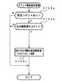
【0130】
図25は、電源基板910の電源監視回路からの電圧低下信号にもとづくNMIに応じて実行される停電発生NMI処理の一例を示すフローチャートである。停電発生NMI処理において、CPU56は、まず、停電時などの電源断時直前の割込許可/禁止状態をバックアップするために、割込禁止フラグの内容をパリティフラグに格納する(ステップS41)。次いで、割込禁止に設定する(ステップS42)。停電発生NMI処理ではRAM内容の保存を確実にするためにチェックサムの生成処理を行う。その処理中に他の割込処理が行われたのではチェックサムの生成処理が完了しないうちにCPUが動作し得ない電圧にまで低下してしまうことが考えられるので、まず、他の割込が生じないような設定がなされる。なお、停電発生NMI処理におけるステップS44〜S50は、電力供給停止時処理の一例である。
なお、割込処理中では他の割込がかからないような仕様のCPUを用いている場合には、ステップS42の処理は不要である。
【0131】
次いで、CPU56は、バックアップフラグが既にセットされているか否か確認する(ステップS42)。バックアップフラグが既にセットされていれば、以後の処理を行わない。バックアップフラグがセットされていなければ、以下の電力供給停止時処理を実行する。すなわち、ステップS44からステップS50の処理を実行する。
【0132】
まず、各レジスタの内容をバックアップRAM領域に格納する(ステップS44)。その後、バックアップフラグをセットする(ステップS45)。そして、バックアップRAM領域のバックアップチェックデータ領域に適当な初期値を設定し(ステップS46)、初期値およびバックアップRAM領域のデータについて順次排他的論理和をとったあと反転し(ステップS47)、最終的な演算値をバックアップパリティデータ領域に設定する(ステップS48)。また、RAMアクセス禁止状態にする(ステップS49)。電源電圧が低下していくときには、各種信号線のレベルが不安定になってRAM内容が化ける可能性があるが、このようにRAMアクセス禁止状態にしておけば、バックアップRAM内のデータが化けることはない。
【0133】
さらに、CPU56は、主基板31に搭載されている全ての出力ポートに対してクリア信号を出力する。すると、全ての出力ポートは、クリア信号によりクリアされオフ状態とされる(ステップS50)。このように、電源断処理の際に出力ポートをクリアする構成としたことで、停止状態となる前に大入賞口を閉成させることができる。さらに、停止状態となる前に可変入賞球装置15を閉成させるなど、他の電気部品についても作動を停止させた状態で電源断状態とすることができる。従って、主基板31により制御される各電気部品を適切な動作停止状態とすることができる。なお、出力ポートの一部をクリアする構成としてもよい。
【0134】
次いで、CPU56は、ループ処理にはいる。すなわち、何らの処理もしない状態になる。従って、図6に示されたリセットIC651からのシステムリセット信号によって外部から動作禁止状態にされる前に、内部的に動作停止状態になる。よって、電源断時に確実にCPU56は動作停止する。その結果、上述したRAMアクセス禁止の制御および動作停止制御によって、電源電圧が低下していくことに伴って生ずる可能性がある異常動作に起因するRAMの内容破壊等を確実に防止することができる。
【0135】
なお、この実施の形態では、停電発生NMI処理では最終部でプログラムをループ状態にしたが、ホールト(HALT)命令を発行するように構成してもよい。
【0136】
また、レジスタの内容をRAM領域に格納した後にセットされるバックアップフラグは、上述したように、電源投入時において復旧すべきバックアップデータがあるか否か(停電からの復旧か否か)を判断する際に使用される。また、ステップS41からS50の処理は、CPU56がシステムリセット回路65からのシステムリセット信号を受ける前に完了する。換言すれば、システムリセット回路65からのシステムリセット信号を受ける前に完了するように、電圧監視回路の検出電圧の設定が行われている。
【0137】
この実施の形態では、電力供給停止時処理開始時に、バックアップフラグの確認が行われる。そして、バックアップフラグが既にセットされている場合には電力供給停止時処理を実行しない。上述したように、バックアップフラグは、必要なデータのバックアップが完了し、その後電力供給停止時処理が完了したことを示すフラグである。従って、例えば、リセット待ちのループ状態で何らかの原因で再度NMIが発生したとしても、電力供給停止時処理が重複して実行されてしまうようなことはない。
【0138】
ただし、割込処理中では他の割込がかからないような仕様のCPUを用いている場合には、ステップS43の判断は不要である。
【0139】
図26は、バックアップパリティデータ作成方法の一例を説明するための説明図である。ただし、図26に示す例では、簡単のために、バックアップデータRAM領域のデータのサイズを3バイトとする。電源電圧低下にもとづく停電発生処理において、図26に示すように、バックアップチェックデータ領域に、初期データ(この例では00H)が設定される。次に、「00H」と「F0H」の排他的論理和がとられ、その結果と「16H」の排他的論理和がとられる。さらに、その結果と「DFH」の排他的論理和がとられる。そして、その結果(この例では「39H」)を反転して得られた値(この例では「C6H」)がバックアップパリティデータ領域に設定される。
【0140】
電源が再投入されたときには、停電復旧処理においてパリティ診断が行われる。バックアップ領域の全データがそのまま保存されていれば、電源再投入時に、図26に示すようなデータがバックアップ領域に設定されている。
【0141】
ステップS4の処理において、CPU56は、電源発生NMI処理にて実行された処理と同様の処理を行う。すなわち、バックアップチェックデータ領域に、初期データ(この例では00H)が設定され、「00H」と「F0H」の排他的論理和がとられ、その結果と「16H」の排他的論理和がとられる。さらに、その結果と「DFH」の排他的論理和がとられる。そして、その結果(この例では「39H」)を反転した最終演算結果を得る。バックアップ領域の全データがそのまま保存されていれば、最終的な演算結果は、「C6H」、すなわちバックアップチェックデータ領域に設定されているデータと一致する。バックアップRAM領域内のデータにビット誤りが生じていた場合には、最終的な演算結果は「C6H」にならない。
【0142】
よって、CPU56は、最終的な演算結果とバックアップチェックデータ領域に設定されているデータとを比較して、一致すればパリティ診断正常とする。一致しなければ、パリティ診断異常とする。
【0143】
以上のように、この実施の形態では、遊技制御手段には、遊技機の電源が断しても、所定期間電源バックアップされる記憶手段(この例ではバックアップRAM)が設けられ、電源投入時に、CPU56(具体的にはCPU56が実行するプログラム)は、記憶手段がバックアップ状態にあればバックアップデータにもとづいて遊技状態を回復させる遊技状態復旧処理(ステップS6)を行うように構成される。
【0144】
この実施の形態では、図7に示されたように電源基板910に電源監視回路が搭載され、図6に示されたように主基板31にシステムリセット回路65が搭載されている。そして、電源電圧が低下していくときに、システムリセット回路65がローレベルのシステムリセット信号を発生する時期は、電源監視回路(この例では電源監視用IC902)がローレベルのNMI割込信号を発生する時期よりも遅くなるように設定されている。さらに、システムリセット回路65からのローレベルのシステムリセット信号は、CPU56のリセット端子に入力されている。
【0145】
すると、CPU56は、電源監視手段(電源監視用IC902)からの電圧低下信号にもとづいて停電発生処理(電力供給停止時処理)を実行した後にループ状態に入るのであるが、ループ状態において、リセット状態に入ることになる。すなわち、CPU56の動作が完全に停止する。+5V電源電圧値以下においては、CPU56の正常な動作が担保できない(即ち、動作の管理ができない状態が発生する)が、CPU56は正常に動作できる電源が供給されている状態でリセット状態になるので、不定データにもとづいて異常動作してしまうことは防止される。
【0146】
このように、この実施の形態では、CPU56が、電源監視回路からの検出出力の入力に応じてループ状態に入るとともに、システムリセット回路65からの検出出力の入力に応じてシステムリセットされるように構成されている。従って、電源断時に確実なデータ保存が行われ、遊技者に不利益がもたらされることが防止される。
【0147】
なお、この実施の形態では、電源監視用IC902と、システムリセット回路65は、同一の電源電圧を監視しているが、異なる電源電圧を監視してもよい。例えば、電源基板910の電源監視回路が+30V電源電圧を監視し、システムリセット回路65が+5V電源電圧を監視してもよい。そして、システムリセット回路65がローレベルのシステムリセット信号を発生するタイミングは電源監視回路がNMI割込信号を発生するタイミングに対して遅くなるように、システムリセット回路65のしきい値レベル(システムリセット信号を発生する電圧レベル)が設定される。例えば、しきい値は4.25Vである。4.25Vは、通常時の電圧より低いが、CPU56が暫くの間動作しうる程度の電圧である。なお、システムリセット回路65に設けられた遅延手段の遅延時間(本例では、コンデンサの容量)を調整して、システムリセット回路65がローレベルのシステムリセット信号を発生するタイミングを電源監視回路がNMI割込信号を発生するタイミングに対して遅らせるようにしてもよい。
【0148】
また、上記の実施の形態では、CPU56は、マスク不能割込端子(NMI端子)を介して電源基板からのNMI割込信号(電源監視手段からのNMI割込信号)を検知したが、NMI割込信号をマスク可能割込割込端子(IRQ端子)に導入してもよい。その場合には、割込処理(IRQ処理)で電力供給停止時処理が実行される。また、入力ポートを介して電源基板からのNMI割込信号を検知してもよい。その場合には、メイン処理において入力ポートの監視が行われる。
【0149】
また、NMI割込信号に変えて、IRQ端子を介して電源基板からの割込信号を検知する場合に、メイン処理のステップS11における遊技制御処理の開始時にIRQ割込マスクをセットし、遊技制御処理の終了時にIRQ割込マスクを解除するようにしてもよい。そのようにすれば、遊技制御処理の開始前および終了後に割込がかかることになって、遊技制御処理が中途で中断されることはない。従って、払出制御コマンドを払出制御基板37に送出しているときなどにコマンド送出が中断されてしまうようなことはない。よって、停電が発生するようなときでも、払出制御コマンド等は確実に送出完了する。
【0150】
また、この実施の形態では、停電発生処理(電力供給停止時処理)において、既にデータがバックアップされ電力供給停止時処理が既に実行されたことを示すバックアップフラグがセットされている場合には電力供給停止時処理を実行しないように構成されている。電源が断する過程では、再度NMIが発生する可能性がある。すると、停電発生処理においてバックアップフラグの確認を行わない場合には、再度発生したNMIによって再度電力供給停止時処理が実行される。
【0151】
最初に実行された正規の電力供給停止時処理では、レジスタの内容をバックアップRAMに格納する処理が行われる(図25におけるステップS44参照)。最初に実行された正規の電力供給停止時処理後のリセット待ちの状態では電源電圧は徐々に低下していくので、レジスタの内容が破壊される可能性もある。すなわち、レジスタ値は、電源断が検出されたときの状態(最初にNMIが発生したとき)から変化している可能性がある。そのような状態で再度電力供給停止時処理が実行されると、電源断が検出されたときの状態のレジスタ値とは異なる値がバックアップRAMに格納されてしまう。すると、電源復旧時に実行される停電復旧処理において、電源断が検出されたときの状態のレジスタ値とは異なる値がレジスタに復旧されてしまう。その結果、電源断時の遊技状態とは異なる遊技状態が再現されてしまう可能性が生ずる。
【0152】
以下、遊技状態復旧処理について説明する。
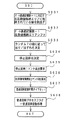
図27は、図8のステップS6に示された遊技状態復旧処理の一例を示すフローチャートである。この例では、CPU56は、バックアップRAMに保存されていた値を各レジスタに復元する(ステップS51)。そして、バックアップRAMに保存されていたデータにもとづいて停電時の遊技状態を確認して復帰させる。すなわち、バックアップRAMに保存されていたデータにもとづいて、ソレノイド回路59を介してソレノイド16やソレノイド21を駆動し、始動入賞口14や開閉板20の開閉状態の復旧を行う(ステップS52,S53)。また、電源断中でも保存されていた特別図柄プロセスフラグおよび普通図柄プロセスフラグの値に応じて、電源断時の特別図柄プロセス処理の進行状況および普通図柄プロセス処理の進行状況に対応した制御コマンドを、表示制御基板80、ランプ制御基板35および音声制御基板70に送出する(ステップS53)。
【0153】
以上のように、遊技状態復旧処理では、復元された内部状態に応じて、各種電気部品の状態復元が行われるとともに、表示制御基板80、ランプ制御基板35および音声制御基板70に対して、制御状態を電源断時の状態に戻すための制御コマンド(電源断時の制御状態を生じさせるための制御コマンド)が送出される。そのような制御コマンドは、一般に、電源断前に最後に送出された1つまたは複数の制御コマンドである。
【0154】
その結果、この実施の形態では、遊技状態復旧処理によって、以下のような状態復旧が可能である。
【0155】
始動入賞口14および大入賞口(開閉板20)の状態が復元される。表示制御手段によって制御される普通図柄の表示状態(可変表示器10の表示状態)は、電源断時に変動中であった場合を除いて復元される。表示制御手段によって制御される特別図柄の表示状態(可変表示部9の表示状態)は、電源断時に変動中であった場合を除いて復元される。さらに、可変表示部9に表示される背景やキャラクタは、特別図柄変動中および大当り遊技中であった場合を除いて復元される。
【0156】
特別図柄の変動中に電源断となった場合には、可変表示パターンの変動時間(例えば10秒)および既に実行した時間(例えば4秒)の情報がバックアップされる。そして、主基板31は、復旧時に、表示パターンを示す表示制御コマンドおよび停止図柄を示す表示制御コマンドを表示制御基板80に出力し、残り時間(上述の例では6秒)経過後に、図柄を停止させるため表示制御コマンドを出力する。従って、特別図柄の表示状態は、電源断時に特別図柄の変動中であった場合には、復旧時に、表示されていない残りの時間(上述の例では6秒)につき可変表示が実行される。なお、復旧時に表示制御基板80に対して出力される表示パターンを示す表示制御コマンドは、電源断前に出力された表示パターンを示す表示制御コマンドと同じものであってもよいが、「停電復旧中です」のような画像を表示させるためのコマンドとしてもよい。この場合、「停電復旧中です」の表示は、残りの時間(上述の例では6秒)表示される。なお、特別図柄の変動中に電源断となった場合の、普通図柄の表示状態にについても、上述と同様の制御が行われる。
【0157】
なお、大当り遊技中に電源断となった場合にも、上述した特別図柄の変動中に電源断となった場合と同様に、ラウンド中あるいはラウンド間のインターバルの残り時間について、復旧時に、表示、音、ランプ、ソレノイド21などを制御するが、主基板31は、表示制御基板80に対して電源断前に出力した確定時の図柄(停止図柄)を指定する表示制御コマンドを出力する。これにより、ラウンド中あるいはラウンド間の大当り図柄による演出が可能となり(大当り図柄で大当り演出する機種について)、また、大当り終了後の変動開始時に表示する図柄も表示制御基板80が認識することができる。
【0158】
ランプ制御手段が制御する装飾ランプ25、始動記憶表示器18、ゲート通過記憶表示器41、賞球ランプ51および球切れランプ52の表示状態が復元される。遊技効果ランプ・LED28a,28b,28cの表示状態は、特別図柄変動中および大当り遊技中であった場合を除いて復元される。ただし、電源断時に大当り遊技中であった場合には、各制御区間の最初の状態に復元可能である。各制御区間とは、例えば、大当り開始報知状態、大入賞口開放前状態、大入賞口開放中状態、大当り終了報知状態である。なお、特別図柄変動中に電源断となったあと復旧した場合には、上述した可変表示部9や可変表示装置10の表示制御と同様に、残り時間分だけ遊技効果ランプ・LED28a,28b,28cの表示状態を制御するようにしてもよいが、消灯または停電復旧時特有のパターンで点灯/点滅させるようにしてもよい。
【0159】
音声制御手段が制御する音発生状態は、特別図柄変動中および大当り遊技中であった場合を除いて復元される。ただし、電源断時に大当り遊技中であった場合には、各制御区間の最初の状態に復元可能である。なお、特別図柄変動中に電源断となったあと復旧した場合には、上述した可変表示部9や可変表示装置10の表示制御と同様に、残り時間分だけ音発生状態を制御するようにしてもよいが、無音または停電復旧時特有の音声パターン(例えば「停電復旧中です」との音声)を出力するようにしてもよい。
【0160】
なお、この実施の形態では、電源断からの復旧時に、主基板31の遊技制御手段から表示制御手段、ランプ制御手段および音声制御手段に対して状態復元のための制御コマンドが送出されるが、表示制御手段、ランプ制御手段および音声制御手段が電源バックアップされる場合には、主基板31からの制御コマンドを用いることなく、表示制御手段、ランプ制御手段および音声制御手段が独自に制御状態を復元するように構成してもよい。
【0161】
また、後述するように、払出制御基板37に搭載されている払出制御手段は、電源バックアップされているので、電源断からの復旧時に、賞球払出状態および球貸し制御状態は、電源断時の状態に復旧する。この実施の形態では、発射制御基板は払出制御手段に接続されているので、発射制御基板91における制御状態も同様に復元される。
【0162】
遊技状態を電源断時の状態に復帰させると、この実施の形態では、CPU56は、前回の電源断時の割込許可/禁止状態を復帰させるため、バックアップRAMに保存されていたパリティフラグの値を確認する(ステップS55)。パリティフラグがクリアであれば、割込許可設定を行う(ステップS56)。一方、パリティフラグがオンであれば、そのまま(ステップS1aで設定された割込禁止状態のまま)遊技状態復旧処理を終える。
【0163】
なお、ここでは、遊技状態復旧処理が終了するとメイン処理にリターンするように遊技状態復旧処理プログラムが構成されているが、電力供給停止時処理において保存されているスタックポインタが指すスタックエリア(バックアップRAM領域にある)に記憶されているアドレス(電源断時のNMI割込発生時に実行されていたアドレス)に戻るようにしてもよい。
【0164】
上述したように、初期設定処理を開始したあと、復旧処理を終える前まで、または初期化処理を終える前までの間は、割込禁止状態とする構成としたことで、割込みにより処理が中断されることを防止することができるため、初期設定、バックアップデータ記憶領域の内容に応じて行われる電源断時の状態に復旧させるか否かの判断、および復旧処理(または初期化処理)を確実に完了させることができる。なお、上記のように復旧処理を終える前まで割込禁止状態とする構成とした場合であっても、電源断時の割込禁止/許可状態をパリティフラグによりバックアップしているため、復旧処理において電源断時の割込禁止/許可状態を確実に復旧させることができる。
【0165】
なお、上記の実施の形態では、遊技制御手段において、データ保存処理および復旧処理が行われる場合について説明したが、払出制御手段、音声制御手段、ランプ制御手段および表示制御手段におけるRAMの一部も電源バックアップされ、払出制御手段、表示制御手段、音制御手段およびランプ制御手段も、上述したような処理を行ってもよい。ただし、払出制御手段、表示制御手段、音制御手段およびランプ制御手段は、復旧時にコマンド送出処理を行う必要はない。
【0166】
図28は、払出制御コマンドのコマンド形態の一例を示す説明図である。この実施の形態では、払出制御コマンドは2バイト構成であり、1バイト目はMODE(コマンドの分類)を表し、2バイト目はEXT(コマンドの種類)を表す。なお、図28に示されたコマンド形態は一例であって他のコマンド形態を用いてもよい。
【0167】
図29は、払出制御コマンドの内容の一例を示す説明図である。図29に示された例において、コマンドFF00(H)は、払出可能状態を指定する払出制御コマンドである。コマンドFF01(H)は、払出停止状態を指定する払出制御コマンドである。また、コマンドF0XX(H)は、賞球個数を指定する払出制御コマンドである。2バイト目の「XX」が払出個数を示す。
【0168】
払出制御手段は、主基板31の遊技制御手段からFF01(H)の払出制御コマンドを受信すると賞球払出および球貸しを停止する状態となり、FF00(H)の払出制御コマンドを受信すると賞球払出および球貸しができる状態になる。また、賞球個数を指定する払出制御コマンドを受信すると、受信したコマンドで指定された個数に応じた賞球払出制御を行う。
【0169】
図30は、払出制御コマンドの送出形態の一例を示すタイミング図である。この実施の形態では、払出制御コマンドは2バイト構成であり、例えば、図30に示されるように、払出制御信号の1バイト目および2バイト目が出力されているときに、それぞれINT信号がオン(この例ではローレベル)になる。INT信号のオン期間は例えば1μs以上であり、1バイト目と2バイト目との間には例えば10μs以上の期間があけられる。なお、払出制御コマンドは、1バイト構成としてもよい。
【0170】
なお、払出制御コマンドは、払出制御手段が認識可能に1回だけ送出される。認識可能とは、この例では、INT信号がオン状態になることであり、認識可能に1回だけ送出されるとは、この例では、払出制御信号の1バイト目および2バイト目のそれぞれに応じてINT信号が1回だけオン状態になることである。
【0171】
なお、図31に示すように、払出制御コマンドを1バイト構成としてもよい。その場合、8ビットの払出制御信号CD〜CD7によって払出制御コマンドが出力される。そして、払出制御信号が出力されているときに、INT信号がオン(この例ではローレベル)になる。INT信号のオン期間は例えば1μs以上である。払出制御手段は、INT信号に応じた割込処理によって払出制御信号CD〜CD7を入力する。
【0172】
次に、遊技制御手段以外の電気部品制御手段においてデータ保存や出力ポートのクリアおよび復旧処理が行われる場合の例として、払出制御手段においてデータ保存、出力ポートのクリア、および復旧が行われる場合について説明する。
図32は、払出制御用CPU371周りの一構成例を示すブロック図である。図32に示すように、第1の電源監視回路(第1の電源監視手段)からの電圧低下信号が、バッファ回路960を介して払出制御用CPU371のマスク不能割込端子(XNMI端子)に接続されている。第1の電源監視回路は、遊技機が使用する各種直流電源のうちのいずれかの電源の電圧を監視して電源電圧低下を検出する回路である。この実施の形態では、VSLの電源電圧を監視して電圧値が所定値以下になるとローレベルの電圧低下信号を発生する。VSLは、遊技機で使用される直流電圧のうちで最大のものであり、この例では+30Vである。従って、払出制御用CPU371は、割込処理によって電源断の発生を確認することができる
【0173】
払出制御用CPU371のCLK/TRG2端子には、主基板31からのINT信号が接続されている。CLK/TRG2端子にクロック信号が入力されると、払出制御用CPU371に内蔵されているタイマカウンタレジスタCLK/TRG2の値がダウンカウントされる。そして、レジスタ値が0になると割込が発生する。従って、タイマカウンタレジスタCLK/TRG2の初期値を「1」に設定しておけば、INT信号の入力に応じて割込が発生することになる。
【0174】
払出制御基板37には、システムリセット回路975も搭載されているが、この実施の形態では、システムリセット回路975は、第2の電源監視回路(第2の電源監視手段)も兼ねている。すなわち、リセットIC976は、電源投入時に、外付けのコンデンサに容量で決まる所定時間だけ出力をローレベルとし、所定時間が経過すると出力をハイレベルにする。また、リセットIC976は、電源基板910に搭載されている第1の電源監視回路が監視する電源電圧と等しい電源電圧であるVSLの電源電圧を監視して電圧値が所定値(例えば+9V)以下になるとローレベルの電圧低下信号を発生する。従って、電源断時には、リセットIC976からの電圧低下信号がローレベルになることによって払出制御用CPU371がシステムリセットされる。なお、図32に示すように、電圧低下信号はリセット信号と同じ出力信号である。
【0175】
リセットIC976が電源断を検知するための所定値は、通常時の電圧より低いが、払出制御用CPU371が暫くの間動作しうる程度の電圧である。また、リセットIC976が、払出制御用CPU371が必要とする電圧(この例では+5V)よりも高い電圧を監視するように構成されているので、払出制御用CPU371が必要とする電圧に対して監視範囲を広げることができる。従って、より精密な監視を行うことができる。
【0176】
+5V電源から電力が供給されていない間、払出制御用CPU371の内蔵RAMの少なくとも一部は、電源基板から供給されるバックアップ電源がバックアップ端子に接続されることによってバックアップされ、遊技機に対する電源が断しても内容は保存される。そして、+5V電源が復旧すると、システムリセット回路975からリセット信号が発せられるので、払出制御用CPU371は、通常の動作状態に復帰する。そのとき、必要なデータがバックアップされているので、停電等からの復旧時には停電発生時の遊技状態に復帰することができる。
【0177】
以上のように、この実施の形態では、電源基板910に搭載されている第1の電源監視回路が、遊技機で使用される直流電圧のうちで最も高い電源VSLの電圧を監視して、その電源の電圧が所定値を下回ったら電圧低下信号(電源断検出信号)を発生する。電源断検出信号が出力されるタイミングでは、IC駆動電圧は、まだ各種回路素子を十分駆動できる電圧値になっている。従って、IC駆動電圧で動作する払出制御基板37の払出制御用CPU371が所定の電力供給停止時処理を行うための動作時間が確保されている。
【0178】
なお、ここでも、第1の電源監視回路は、遊技機で使用される直流電圧のうちで最も高い電源VSLの電圧を監視することになるが、電源断検出信号を発生するタイミングが、IC駆動電圧で動作する電気部品制御手段が所定の電力供給停止時処理を行うための動作時間が確保されるようなタイミングであれば、監視対象電圧は、最も高い電源VSLの電圧でなくてもよい。すなわち、少なくともIC駆動電圧よりも高い電圧を監視すれば、電気部品制御手段が所定の電力供給停止時処理を行うための動作時間が確保されるようなタイミングで電源断検出信号を発生することができる。
【0179】
その場合、上述したように、監視対象電圧は、賞球カウントスイッチ301A等の遊技機の各種スイッチに供給される電圧が+12Vであることから、電源断時のスイッチオン誤検出の防止も期待できる電圧であることが好ましい。すなわち、スイッチに供給される電圧(スイッチ電圧)である+12V電源電圧が落ち始める以前の段階で、電圧低下を検出できることが好ましい。よって、少なくともスイッチ電圧よりも高い電圧を監視することが好ましい。
【0180】
なお、図32に示された構成では、システムリセット回路975は、電源投入時に、コンデンサの容量で決まる期間のローレベルを出力し、その後ハイレベルを出力する。すなわち、リセット解除タイミングは1回だけである。しかし、図6に示された主基板31の場合と同様に、複数回のリセット解除タイミングが発生するような回路構成を用いてもよい。
【0181】
図33は、払出制御用CPU371のメイン処理を示すフローチャートである。メイン処理では、払出制御用CPU371は、まず、必要な初期設定を行う(ステップS701)。
【0182】
図34は、ステップS701の初期設定処理を示すフローチャートである。初期設定処理において、払出制御用CPU371は、まず、割込禁止に設定する(ステップS701a)。次に、払出制御用CPU371は、割込モードを割込モード2に設定し(ステップS701b)、スタックポインタにスタックポインタ指定アドレスを設定する(ステップS701c)。また、払出制御用CPU371は、内蔵デバイスレジスタの初期化(ステップS701d)、CTC(カウンタ/タイマ)およびPIO(パラレル入出力ポート)の初期化(ステップS701e)を行ったあと、RAMをアクセス可能状態に設定する(ステップS701f)。
【0183】
この実施の形態では、タイマ/カウンタ割込としてCH2,CH3のカウントアップにもとづく割込を使用する。CH2のカウントアップにもとづく割込は、上述したタイマカウンタレジスタCLK/TRG2の値が「0」になったときに発生する割込である。従って、ステップS701eにおいて、タイマカウンタレジスタCLK/TRG2に初期値「1」が設定される。また、CH3のカウントアップにもとづく割込は、CPUの内部クロックをカウントダウンしてレジスタ値が「0」になったら発生する割込であり、後述する2msタイマ割込として用いられる。具体的には、CH3のレジスタ値はシステムクロックの1/256周期で減算される。ステップS701eにおいて、CH3のレジスタには、初期値として2msに相当する値が設定される。なお、CH2に関する割込番地は0074Hであり、CH3に関する割込番地は0076Hである。
【0184】
そして、払出制御用CPU371は、払出制御用のバックアップRAM領域にバックアップデータが存在しているか否かの確認を行う(ステップS702)。すなわち、例えばバックアップRAM領域に形成されている後述する総合個数記憶または貸し球個数記憶(図37参照)を確認して、未払出の賞球個数および貸し球個数に関するバックアップデータがないかどうか確認する。不測の電源断が生じた場合には、多くの場合何らかのデータがバックアップRAM領域に保存されており、バックアップRAM領域のデータは保存されていたはずであるから、後に復旧した場合の確認結果の多くはバックアップデータありとなる。バックアップデータなしという確認結果であれば、前回の電源オフ時に未払出の遊技球がなかったことになり、内部状態を電源断時の状態に戻す必要がないので、停電復旧時でない電源投入時に実行される初期化処理を実行する(ステップS702,S703)。なお、本例では、バックアップRAM領域にバックアップデータが存在しているか否かは、電源断時にバックアップRAM領域に設定されるバックアップフラグによって確認する。
【0185】
バックアップRAM領域にバックアップデータが存在している場合には、この実施の形態では、払出制御用CPU371は、バックアップRAM領域のデータチェック(この例ではパリティチェック)を行う(ステップS704)。不測の電源断が生じた後に復旧した場合には、バックアップRAM領域のデータは保存されていたはずであるから、チェック結果は正常になる。チェック結果が正常でない場合には、内部状態を電源断時の状態に戻すことができないので、停電復旧時でない電源投入時に実行される初期化処理を実行する(ステップS705,S703)。
【0186】
チェック結果が正常であれば、払出制御用CPU371は、内部状態を電源断時の状態に戻すための払出状態復旧処理を行う(ステップS706)。そして、バックアップRAM領域に保存されていたPC(プログラムカウンタ)の指すアドレスに復帰する(ステップS707)。
【0187】
通常の初期化処理の実行(ステップS703)を終えると、払出制御用CPU371により実行されるメイン処理は、タイマ割込フラグの監視(ステップS708)の確認が行われるループ処理に移行する。
【0188】
なお、この実施の形態では、ステップS702でバックアップデータの有無を確認したあと、バックアップデータが存在する場合にステップS704でバックアップ領域のチェックを行うようにしていたが、逆に、バックアップ領域のチェック結果が正常であったことを確認したあと、バックアップデータの有無の確認を行うようにしてもよい。また、バックアップデータの有無の確認、またはバックアップ領域のチェックの何れか一方の確認を行うことで、停電復旧処理を実行するか否か判断するよう構成してもよい。
【0189】
また、例えば停電復旧処理を実行するか否か判断する場合のパリティチェック(ステップS704)の際などに、すなわち、遊技状態を復旧するか否か判断する際に、保存されていたRAMデータにおける払出遊技球数データ等によって、遊技機が払出待機状態(払出途中でない状態)であることが確認されたら、払出状態復旧処理を行わずに初期化処理を実行するようにしてもよい。
【0190】
通常の初期化処理では、図35に示すように、レジスタおよびRAMのクリア処理(ステップS901)が行われ、所定の初期値の設定が行われる(ステップS902)。そして、初期設定処理(ステップS701a)において割込禁止とされているので、初期化処理を終える前に割込が許可される(ステップS903)。
【0191】
この実施の形態では、払出制御用CPU371の内部タイマ(CH3)が繰り返しタイマ割込を発生するように設定される。また、繰り返し周期は2msに設定される。そして、図36に示すように、タイマ割込が発生すると、払出制御用CPU371は、タイマ割込フラグをセットする(ステップS711)。なお、2msタイマ割込処理において、必要ならば、CH3のレジスタに対して初期値再設定が行われる。
【0192】
払出制御用CPU371は、ステップS708において、タイマ割込フラグがセットされたことを検出すると、タイマ割込フラグをリセットするとともに(ステップS709)、払出制御処理を実行する(ステップS710)。以上の制御によって、この実施の形態では、払出制御処理は2ms毎に起動されることになる。なお、この実施の形態では、タイマ割込処理ではフラグセットのみがなされ、払出制御処理はメイン処理において実行されるが、タイマ割込処理で払出制御処理を実行してもよい。
【0193】
払出制御用CPU371は、電源投入時に、バックアップRAM領域のデータを確認するだけで、通常の初期設定処理を行うのか払出中の状態を復元するのか決定できる。すなわち、簡単な判断によって、未払出の遊技球について払出処理再開を行うことができる。
【0194】
また、本例では、払出制御用CPU371も、主基板31のCPU56と同様に、パリティチェックコードによって記憶内容保存の確実化を図っている。
【0195】
図37は、払出制御用CPU371が内蔵するRAMの使用例を示す説明図である。この例では、バックアップRAM領域に総合個数記憶(例えば2バイト)および貸し球個数記憶が形成されている。総合個数記憶は、主基板31の側から指示された払出個数の総数を記憶するものである。貸し球個数記憶は、未払出の球貸し個数を記憶するものである。
【0196】
図38は、割込処理による払出制御コマンド受信処理を示すフローチャートである。主基板31からの払出制御用のINT信号は払出制御用CPU371のCLK/TRG2端子に入力されている。よって、主基板31からのINT信号がオン状態になると、払出制御用CPU371に割込がかかり、図38に示す払出制御コマンドの受信処理が開始される。この実施の形態では、受信した払出制御コマンドを格納するための12バイトの確定コマンドバッファ領域が設けられている。そして、受信した払出制御コマンドの格納位置を示すためにコマンド受信個数カウンタが用いられる。なお、払出制御コマンドは、2バイト構成であるから、実質的には6個の払出制御コマンドを確定コマンドバッファ領域に格納可能である。
【0197】
払出制御コマンドの受信処理において、払出制御用CPU371は、まず、払出制御コマンドデータの入力に割り当てられている入力ポート372aからデータを読み込む(ステップS851)。そして、2バイト構成の払出制御コマンドのうちの1バイト目であるか否か確認する(ステップS852)。1バイト目であるか否かは、受信したコマンドの先頭ビットが「1」であるか否かで確認できる。先頭ビットが「1」であるのは、2バイト構成である払出制御コマンドのうちのMODEバイト(1バイト目)のはずである(図28参照)。先頭ビットが「1」であれば、有効な1バイト目を受信したとして、受信したコマンドを確定コマンドバッファ領域におけるコマンド受信個数カウンタが示す確定コマンドバッファに格納する(ステップS853)。
【0198】
払出制御コマンドのうちの1バイト目でなければ、1バイト目を既に受信したか否か確認する(ステップS854)。既に受信したか否かは、受信バッファ(ステップS853における確定コマンドバッファ)に有効なデータが設定されているか否かで確認できる。
【0199】
1バイト目を既に受信している場合には、受信した1バイトのうちの先頭ビットが「0」であるか否か確認する。そして、先頭ビットが「0」であれば、有効な2バイト目を受信したとして、受信したコマンドを、確定コマンドバッファ領域におけるコマンド受信個数カウンタ+1が示す確定コマンドバッファに格納する(ステップS855)。先頭ビットが「0」であるのは、2バイト構成である払出制御コマンドのうちのEXTバイト(2バイト目)のはずである(図28参照)。なお、図示はしないが、ステップS854のYのあとの確認で、受信した1バイトのうちの先頭ビットが「0」でなければ、処理を終了する。
【0200】
ステップS855において、2バイト目のコマンドデータを格納すると、コマンド受信個数カウンタに2を加算する(ステップS856)。そして、コマンド受信カウンタが12以上であるか否か確認し(ステップS857)、12以上であればコマンド受信個数カウンタをクリアする(ステップS858)。
【0201】
図39は、ステップS710の払出制御処理を示すフローチャートである。払出制御処理において、払出制御用CPU371は、まず、中継基板72を介して入力ポート372bに入力される賞球カウントスイッチ301A、球貸しカウントスイッチ301Bがオンしたか否かを判定する(スイッチ処理:ステップS751)。
【0202】
次に、払出制御用CPU371は、センサ(例えば、払出モータ289の回転数を検出するモータ位置センサ)からの信号入力状態を確認してセンサの状態判定などを行う(入力判定処理:ステップS752)。払出制御用CPU371は、さらに、受信した払出制御コマンドを解析し、解析結果に応じた処理を実行する(コマンド解析実行処理:ステップS753)。
【0203】
次いで、払出制御用CPU371は、主基板31より受信した払出停止指示コマンドに応じて払出停止状態に設定し、あるいは受信した払出開始指示コマンドに応じて払出停止状態の解除を行う(ステップS754)。また、プリペイドカードユニット制御処理を行う(ステップS755)。
【0204】
また、払出制御用CPU371は、球貸し要求に応じて貸し球を払い出す制御を行う(ステップS756)。さらに、払出制御用CPU371は、総合個数記憶に格納された個数の賞球を払い出す賞球制御処理を行う(ステップS757)。そして、払出制御用CPU371は、出力ポート372cおよび中継基板72を介して球払出装置97の払出機構部分における払出モータ289に向けて駆動信号を出力し、ステップS756の球貸し制御処理またはステップS757の賞球制御処理で設定された回転数分払出モータ289を回転させる払出モータ制御処理を行う(ステップS758)。
【0205】
なお、この実施の形態では、払出モータ289としてステッピングモータが用いられ、払出モータ289を制御するために1−2相励磁方式が用いられる。従って、具体的には、払出モータ制御処理において、8種類の励磁パターンデータが繰り返し払出モータ289に出力される。また、この実施の形態では、各励磁パターンデータが4msずつ出力される。
【0206】
次いで、エラー検出処理が行われ、その結果に応じてエラー表示LED374に所定の表示を行う(エラー処理:ステップS759)。検出されるエラーとして、例えば、次の8種類がある。
【0207】
賞球経路エラー:賞球払出動作終了したとき、または払出モータ289が1回転したときに賞球カウントスイッチ301Aが1個も遊技球の通過を検出しなかったとき。エラー表示LED374に「0」が表示される。
【0208】
球貸し経路エラー:球貸しの払出動作終了したとき、または払出モータ289が1回転したときに球貸しカウントスイッチ301Bが1個も遊技球の通過を検出しなかったとき。エラー表示LED374に「1」が表示される。
【0209】
賞球カウントスイッチ球詰まりエラー:賞球カウントスイッチ301Aが0.5秒以上オンを検出したとき。エラー表示LED374に「2」が表示される。
【0210】
球貸しカウントスイッチ球詰まりエラー:球貸しカウントスイッチ301Bが0.5秒以上オンを検出したとき。エラー表示LED374に「3」が表示される。
【0211】
払出モータ球噛みエラー:払出モータ289が正常に回転しないとき。具体的には、払出モータ位置センサのオンが所定期間以上継続したり、オフが所定期間以上継続した場合。エラー表示LED374に「4」が表示される。なお、払出モータ球噛みエラーが生じた場合には、払出制御用CPU371は、50msの基準励磁相の出力を行った後、1−2相励磁の励磁パターンデータのうちの4種類の励磁パターンデータを8ms毎に出力することによる払出モータ289の逆回転と正回転を繰り返す。
【0212】
プリペイドカードユニット未接続エラー:VL信号のオフが検出されたとき。エラー表示LED374に「5」が表示される。
【0213】
プリペイドカードユニット通信エラー:規定のタイミング以外でプリペイドカードユニット50から信号出力されたことを検出したとき。エラー表示LED374に「6」が表示される。
【0214】
払出停止状態:主基板31から払出停止を示す払出制御コマンドを受信したとき。エラー表示LED374に「7」が表示される。なお、主基板31から払出開始を示す払出制御コマンドを受信したときには、その時点から2002ms後に、払出停止状態から払出可能状態に復帰する。
【0215】
さらに、外部接続端子(図示せず)から出力する情報信号を制御する処理を行う(出力処理:ステップS760)。なお、情報信号は、貸し球の払出一単位(例えば25個)ごとに所定時間オンとなり、続いて所定時間オフを出力する信号である。
【0216】
図40は、ステップS751のスイッチ処理の一例を示すフローチャートである。スイッチ処理において、払出制御用CPU371は、賞球カウントスイッチ301Aがオン状態を示しているか否か確認する(ステップS751a)。オン状態を示していれば、払出制御用CPU371は、賞球カウントスイッチオンカウンタを+1する(ステップS751b)。賞球カウントスイッチオンカウンタは、賞球カウントスイッチ301Aのオン状態を検出した回数を計数するためのカウンタである。
【0217】
そして、賞球カウントスイッチオンカウンタの値をチェックし(ステップS751c)、その値が2になっていれば、一個の賞球の払出が行われたと判断する。一個の賞球の払出が行われたと判断した場合には、払出制御用CPU371は、賞球未払出カウンタ(総合個数記憶に格納されている賞球数)を−1する(ステップS751d)。
【0218】
ステップS751aにおいて賞球カウントスイッチ301Aがオン状態でないことが確認されると、払出制御用CPU371は、賞球カウントスイッチオンカウンタをクリアする(ステップS751e)。そして、この実施の形態では、球貸しカウントスイッチ301Bがオン状態を示しているか否か確認する(ステップS751f)。オン状態を示していれば、払出制御用CPU371は、球貸しカウントスイッチオンカウンタを+1する(ステップS751g)。球貸しカウントスイッチオンカウンタは、球貸しカウントスイッチ301Bのオン状態を検出した回数を計数するためのカウンタである。
【0219】
そして、球貸しカウントスイッチオンカウンタの値をチェックし(ステップS751h)、その値が2になっていれば、一個の貸し球の払出が行われたと判断する。一個の貸し球の払出が行われたと判断した場合には、払出制御用CPU371は、貸し球未払出個数カウンタ(貸し球個数記憶に格納されている貸し球数)を−1する(ステップS751i)。
【0220】
ステップS751fにおいて球貸しカウントスイッチ301Bがオン状態でないことが確認されると、払出制御用CPU371は、球貸しカウントスイッチオンカウンタをクリアする(ステップS751j)。
【0221】
図41は、ステップS753のコマンド解析実行処理の一例を示すフローチャートである。コマンド解析実行処理において、払出制御用CPU371は、確定コマンドバッファ領域中に受信コマンドがあるか否かの確認を行う(ステップS753a)。受信コマンドがあれば、受信した払出制御コマンドが払出個数指示コマンドであるか否かの確認を行う(ステップS753b)。なお、確定コマンドバッファ領域中に複数の受信コマンドがある場合には、受信した払出制御コマンドが払出個数指示コマンドであるか否かの確認は、最も前に受信された受信された受信コマンドについて行われる。
【0222】
受信した払出制御コマンドが払出個数指示コマンドであれば、払出個数指示コマンドで指示された個数を総合個数記憶に加算する(ステップS753c)。すなわち、払出制御用CPU371は、主基板31のCPU56から送られた払出個数指示コマンドに含まれる賞球数をバックアップRAM領域(総合個数記憶)に記憶する。
【0223】
なお、払出制御用CPU371は、必要ならば、コマンド受信個数カウンタの減算や確定コマンドバッファ領域における受信コマンドシフト処理を行う。
【0224】
図42は、ステップS754の払出停止状態設定処理の一例を示すフローチャートである。払出停止状態設定処理において、払出制御用CPU371は、確定コマンドバッファ領域中に受信コマンドがあるか否かの確認を行う(ステップS754a)。確定コマンドバッファ領域中に受信コマンドがあれば、受信した払出制御コマンドが払出停止指示コマンドであるか否かの確認を行う(ステップS754b)。払出停止指示コマンドであれば、払出制御用CPU371は、払出停止状態に設定する(ステップS754c)。
【0225】
ステップS754bで受信コマンドが払出停止指示コマンドでないことを確認すると、受信した払出制御コマンドが払出開始指示コマンドであるか否かの確認を行う(ステップS754d)。払出開始指示コマンドであれば、払出停止状態を解除する(ステップS754e)。
【0226】
図43は、ステップS755のプリペイドカードユニット制御処理の一例を示すフローチャートである。プリペイドカードユニット制御処理において、払出制御用CPU371は、カードユニット制御用マイクロコンピュータより入力されるVL信号を検知したか否かを確認する(ステップS755a)。VL信号を検知していなければ、VL信号非検知カウンタを+1する(ステップS755b)。また、払出制御用CPU371は、VL信号非検知カウンタの値が本例では125であるか否か確認する(ステップS755c)。VL信号非検知カウンタの値が125であれば、払出制御用CPU371は、発射制御基板91への発射制御信号出力を停止して、駆動モータ94を停止させる(ステップS755d)。
【0227】
以上の処理によって、125回(2ms×125=250ms)継続してVL信号のオフが検出されたら、球発射禁止状態に設定される。
【0228】
ステップS755aにおいてVL信号を検知していれば、払出制御用CPU371は、VL信号非検知カウンタをクリアする(ステップS755e)。そして、払出制御用CPU371は、発射制御信号出力を停止していれば(ステップS755f)、発射制御基板91への発射制御信号出力を開始して駆動モータ94を動作可能状態にする(ステップS755g)。
【0229】
図44および図45は、ステップS756の球貸し制御処理の一例を示すフローチャートである。なお、この例では、連続的な払出数の最大値を貸し球の一単位(本例では25個)としているが、他の数であっても良い。
【0230】
球貸し制御処理において、払出制御用CPU371は、貸し球払出中であるか否かの確認を行い(ステップS511)、貸し球払出中であれば図45に示す球貸し中の処理に移行する。なお、この確認は、後述する球貸し処理中フラグの状態により判断される。貸し球払出中でなければ、賞球の払出中であるか否かの確認をする(ステップS512)。この確認は、後述する賞球処理中フラグの状態により判断される。
【0231】
貸し球払出中でも賞球払出中でもなければ、払出制御用CPU371は、カードユニット50から球貸し要求があったか否かを確認し(ステップS513)、要求があれば、球貸し処理中フラグをオンするとともに(ステップS514)、25(球貸し一単位数:ここでは100円分)をバックアップRAM領域の貸し球個数記憶に設定する(ステップS515)。そして、払出制御用CPU371は、EXS信号をオンする(ステップS516)。そして、球払出装置97の下方の球振分部材311を球貸し側に設定するために振分用ソレノイド310を駆動する(ステップS517)。また、払出モータ289をオンして(ステップS518)、図45に示す球貸し中の処理に移行する。
【0232】
なお、払出モータ289をオンするのは、厳密には、カードユニット50が受付を認識したことを示すためにBRQ信号をOFFとしてからである。なお、球貸し処理中フラグはバックアップRAM領域に設定される。
【0233】
図45は、払出制御用CPU371による払出制御処理における球貸し中の処理を示すフローチャートである。球貸し処理では、払出モータ289がオンしていなければオンする。なお、この実施の形態では、ステップS751のスイッチ処理で、球貸しカウントスイッチ301Bの検出出力による遊技球の払出がなされたか否かの確認を行うため、球貸し制御処理では貸し球個数記憶の減算などは行われない。球貸し制御処理において、払出制御用CPU371は、貸し球通過待ち時間中であるか否かの確認を行う(ステップS519)。貸し球通過待ち時間中でなければ、貸し球の払出を行い(ステップS520)、払出モータ289の駆動を終了すべきか(一単位の払出動作が終了したか)否かの確認を行う(ステップS521)。具体的には、所定個数の払出に対応した回転が完了したか否かを確認する。所定個数の払出に対応した回転は、払出モータ位置センサの出力によって監視される。所定個数の払出に対応した回転が完了した場合には、払出制御用CPU371は、払出モータ289の駆動を停止し(ステップS522)、貸し球通過待ち時間の設定を行う(ステップS523)。
【0234】
なお、ステップS520の球貸し処理では、払出モータ位置センサのオンとオフとがタイマ監視されるが、所定時間以上のオン状態またはオフ状態が継続したら、払出制御用CPU371は、払出モータ球噛みエラーが生じたと判断する。
【0235】
ステップS519で貸し球通過待ち時間中であれば、払出制御用CPU371は、貸し球通過待ち時間が終了したか否かの確認を行う(ステップS524)。貸し球通過待ち時間は、最後の払出球が払出モータ289によって払い出されてから球貸しカウントスイッチ301Bを通過するまでの時間である。貸し球通過待ち時間の終了を確認すると、一単位の貸し球は全て払い出された状態であるので、カードユニット50に対して次の球貸し要求の受付が可能になったことを示すためにEXS信号をオフにする(ステップS524)。また、振分ソレノイドをオフするとともに(ステップS525)、払出モータ289をオフして(ステップS526)、さらに球貸し処理中フラグをオフする(ステップS527)。なお、貸し玉通過待ち時間が経過するまでに最後の払出球が球貸しカウントスイッチ301Bを通過しなかった場合には、球貸し経路エラーとされる。また、この実施の形態では、賞球も球貸しも同じ払出装置で行われる。
【0236】
なお、球貸し要求の受付を示すEXS信号をオフにした後、所定期間内に再び球貸し要求信号であるBRQ信号がオンしたら、振分ソレノイドおよび払出モータをオフせずに球貸し処理を続行するようにしてもよい。すなわち、所定単位(この例では100円単位)毎に球貸し処理を行うのではなく、球貸し処理を連続して実行するように構成することもできる。
【0237】
貸し球個数記憶の内容は、遊技機の電源が断しても、所定期間電源基板910のバックアップ電源によって保存される。従って、所定期間中に電源が回復すると、払出制御用CPU371は、貸し球個数記憶の内容にもとづいて球貸し処理を継続することができる。
【0238】
図46および図47は、ステップS757の賞球制御処理の一例を示すフローチャートである。なお、この例では、連続的な払出数の最大値を貸し球の一単位と同数(本例では25個)としているが、他の数であっても良い。
【0239】
賞球制御処理において、払出制御用CPU371は、貸し球払出中であるか否かの確認を行う(ステップS531)。なお、この確認は、球貸し処理中フラグの状態により判断される。貸し球払出中でなければ賞球の払出中であるか否か確認し(ステップS532)、賞球の払出中であれば図47に示す賞球中の処理に移行する。この確認は、後述する賞球処理中フラグの状態により判断される。
【0240】
貸し球払出中でも賞球払出中でもなければ、払出制御用CPU371は、カードユニット50からの球貸し準備要求があるか否かの確認を行う(ステップS533)。なお、この確認は、払出制御用CPU371により、カードユニット50から入力されるBRDY信号のオン(要求あり)またはオフ(要求なし)を確認することにより行われる。
【0241】
カードユニット50からの球貸し準備要求がなければ、払出制御用CPU371は、総合個数記憶に格納されている賞球数(未払出の賞球数)が0でないか否かの確認を行う(ステップS534)。総合個数記憶に格納されている賞球数が0でなければ、賞球制御用CPU371は、賞球処理中フラグをオンし(ステップS535)、総合個数記憶の値が本例では25以上であるか否かの確認を行う(ステップS536)。なお、賞球処理中フラグは、バックアップRAM領域に設定される。
【0242】
総合個数記憶に格納されている賞球数が25以上であると、払出制御用CPU371は、25個分の遊技球を払い出すまで払出モータ289を回転させるよう駆動信号出力するために、25個払出動作の設定を行う(ステップS537)。一方、総合個数記憶に格納されている賞球数が25以上でなければ、払出制御用CPU371は、総合個数記憶に格納されている全ての遊技球を払い出すまで払出モータ289を回転させるよう駆動信号出力するために、全個数払出動作の設定を行う(ステップS538)。そして、ステップS537またはステップS538での設定に従って払出モータ289をオンする(ステップS538)。なお、振分ソレノイドはオフ状態であるため、球払出装置97の下方の球振分部材は賞球側に設定されている。そして、図47に示す賞球制御処理における賞球払出中の処理に移行する。
【0243】
図47は、払出制御用CPU371による払出制御処理における賞球中の処理の一例を示すフローチャートである。賞球制御処理では、払出モータ289がオンしていなければオンする。なお、この実施の形態では、ステップS751のスイッチ処理で、賞球カウントスイッチ301Aの検出出力による遊技球の払出がなされたか否かの確認を行うため、賞球制御処理では総合個数記憶の減算などは行われない。賞球中の処理において、払出制御用CPU371は、賞球通過待ち時間中であるか否かの確認を行う(ステップS540)。賞球通過待ち時間中でなければ、賞球払出を行い(ステップS541)、払出モータ289の駆動を終了すべきか(本例では25個または25個未満の所定の個数の払出動作が終了したか)否かの確認を行う(ステップS542)。具体的には、所定個数の払出に対応した回転が完了したか否かを確認する。所定個数の払出に対応した回転は、払出モータ位置センサの出力によって監視される。所定個数の払出に対応した回転が完了した場合には、払出制御用CPU371は、払出モータ289の駆動を停止し(ステップS543)、賞球通過待ち時間の設定を行う(ステップS542)。賞球通過待ち時間は、最後の払出球が払出モータ289によって払い出されてから賞球カウントスイッチ301Aを通過するまでの時間である。
【0244】
一方、ステップS540にて賞球通過待ち時間中であれば、払出制御用CPU371は、賞球通過待ち時間が終了したか否かの確認を行う(ステップS544)。貸し球通過待ち時間の終了を確認すると、ステップS537またはステップS538で設定された賞球が全て払い出された状態であるので、払出モータ289をオフするとともに(ステップS545)、賞球処理中フラグをオフする(ステップS546)。なお、賞球通過待ち時間が経過するまでに最後の払出球が賞球カウントスイッチ301Aを通過しなかった場合には、賞球経路エラーとされる。
【0245】
また、この実施の形態では、ステップS511、ステップS531の判断によって球貸しが賞球処理よりも優先されることになるが、賞球処理が球貸しに優先するようにしてもよい。
【0246】
総合個数記憶および貸し球個数記憶の内容は、遊技機の電源が断しても、所定期間電源基板910のバックアップ電源によって保存される。従って、所定期間中に電源が回復すると、払出制御用CPU371は、総合個数記憶の内容にもとづいて払出処理を継続することができる。
【0247】
なお、払出制御用CPU371は、主基板31から指示された賞球個数を賞球個数記憶で総数として管理したが、賞球数毎(例えば15個、10個、6個)に管理してもよい。例えば、賞球数毎に対応した個数カウンタを設け、払出個数指定コマンドを受信すると、そのコマンドで指定された個数に対応する個数カウンタを+1する。そして、個数カウンタに対応した賞球払出が行われると、その個数カウンタを−1する(この場合、払出制御処理にて減算処理を行うようにする)。その場合にも、各個数カウンタはバックアップRAM領域に形成される。よって、遊技機の電源が断しても、所定期間中に電源が回復すれば、払出制御用CPU371は、各個数カウンタの内容にもとづいて賞球払出処理を継続することができる。
【0248】
図48は、電源基板910の電源監視回路からの電圧低下信号にもとづくNMIに応じて実行される停電発生NMI処理の一例を示すフローチャートである。なお、この実施の形態では、NMI割込番地は0066Hである。停電発生NMI処理において、払出制御用CPU371は、まず、割込禁止フラグの内容をパリティフラグに格納する(ステップS801)。次いで、割込禁止に設定する(ステップS802)。停電発生NMI処理では、本例では主基板31において実行された処理と同様に、RAM内容の保存を確実にするためのチェックサムの生成処理を行う。その処理中に他の割込処理が行われたのではチェックサムの生成処理が完了しないうちに払出制御用CPU371が動作し得ない電圧にまで低下してしまうことがことも考えられるので、まず、他の割込が生じないような設定がなされる。なお、停電発生NMI処理におけるステップS804〜S810は、電力供給停止時処理の一例である。
【0249】
なお、割込処理中では他の割込がかからないような仕様のCPUを用いている場合には、ステップS802の処理は不要である。
【0250】
次いで、払出制御用CPU371は、バックアップフラグが既にセットされているか否か確認する(ステップS803)。バックアップフラグが既にセットされていれば、以後の処理を行わない。バックアップフラグがセットされていなければ、以下の電力供給停止時処理を実行する。すなわち、ステップS804からステップS810の処理を実行する。
【0251】
まず、各レジスタの内容をバックアップRAM領域に格納する(ステップS804)。その後、バックアップフラグをセットする(ステップS805)。そして、バックアップRAM領域のバックアップチェックデータ領域に適当な初期値を設定し(ステップS806)、初期値およびバックアップRAM領域のデータについて順次排他的論理和をとったあと反転し(ステップS807)、最終的な演算値をバックアップパリティデータ領域に設定する(ステップS808)。また、RAMアクセス禁止状態にする(ステップS809)。電源電圧が低下していくときには、各種信号線のレベルが不安定になってRAM内容が化ける可能性があるが、このようにRAMアクセス禁止状態にしておけば、バックアップRAM内のデータが化けることはない。
【0252】
さらに、払出制御用CPU371は、全ての出力ポート(この実施の形態では、出力ポート372c,372g,372e、およびI/Oポート372fの出力ポート部分)に対してクリア信号を出力する。従って、全ての出力ポートは、クリア信号によりオフ状態とされる(ステップS810)。このように、電源断処理の際に出力ポートをクリアする構成としたことで、停止状態となる前に、例えば、駆動状態にある払出モータ289の作動を停止させることができるなど、各電気部品について作動を停止させた状態で電源断状態とすることができる。従って、払出制御基板37により制御される各電気部品を適切な動作停止状態とすることができる。なお、出力ポートの一部をクリアする構成としてもよい。
【0253】
次いで、払出制御用CPU371は、ループ処理にはいる。すなわち、何らの処理もしない状態になる。従って、図32に示されたリセットIC976からのシステムリセット信号によって外部から動作禁止状態にされる前に、内部的に動作停止状態になる。よって、電源断時に確実に払出制御用CPU371は動作停止する。その結果、上述したRAMアクセス禁止の制御および動作停止制御によって、電源電圧が低下していくことに伴って生ずる可能性がある異常動作に起因するRAMの内容破壊等を確実に防止することができる。
【0254】
なお、この実施の形態では、停電発生NMI処理では最終部でプログラムをループ状態にしたが、ホールト(HALT)命令を発行するように構成してもよい。
【0255】
また、レジスタの内容をRAM領域に格納した後にセットされるバックアップフラグは、上述したように、電源投入時において復旧すべきバックアップデータがあるか否か(停電からの復旧か否か)を判断する際に使用される。また、ステップS801からS810の処理は、払出制御用CPU371がシステムリセット回路975からのシステムリセット信号を受ける前に完了する。換言すれば、システムリセット回路975からのシステムリセット信号を受ける前に完了するように、電圧監視回路の検出電圧の設定が行われている。
【0256】
この実施の形態では、電力供給停止時処理開始時に、バックアップフラグの確認が行われる。そして、バックアップフラグが既にセットされている場合には電力供給停止時処理を実行しない。上述したように、バックアップフラグは、必要なデータのバックアップが完了し、その後電力供給停止時処理が完了したことを示すフラグである。従って、例えば、リセット待ちのループ状態で何らかの原因で再度NMIが発生したとしても、電力供給停止時処理が重複して実行されてしまうようなことはない。
【0257】
ただし、割込処理中では他の割込がかからないような仕様のCPUを用いている場合には、ステップS803の判断は不要である。
【0258】
また、この実施の形態では、払出制御用CPU371は、マスク不能外部割込端子(NMI端子)を介して電源基板からのNMI割込信号(電源監視手段からのNMI割込信号)を検知したが、NMI割込信号をマスク可能割込割込端子(IRQ端子)に導入してもよい。その場合には、IRQ処理によって図48に示された停電発生NMI処理が実行される。また、入力ポートを介してNMI割込信号を検知してもよい。その場合には、払出制御用CPU371が実行するメイン処理において、入力ポートの監視が行われる。
【0259】
図49は、バックアップパリティデータ作成方法の一例を説明するための説明図である。ただし、図49に示す例では、簡単のために、バックアップデータRAM領域のデータのサイズを3バイトとする。電源電圧低下にもとづく停電発生処理において、図49に示すように、バックアップチェックデータ領域に、初期データ(この例では00H)が設定される。次に、「00H」と「F0H」の排他的論理和がとられ、その結果と「16H」の排他的論理和がとられる。さらに、その結果と「DFH」の排他的論理和がとられる。そして、その結果(この例では「39H」)を反転して得られた値(この例では「C6H」)がバックアップパリティデータ領域に設定される。
【0260】
電源が再投入されたときには、停電復旧処理においてパリティ診断が行われる。バックアップ領域の全データがそのまま保存されていれば、電源再投入時に、図49に示すようなデータがバックアップ領域に設定されている。
【0261】
ステップS704の処理において、払出制御用CPU371は、図48のステップS806およびステップS807にて実行された処理と同様の処理を行う。すなわち、バックアップチェックデータ領域に、初期データ(この例では00H)が設定され、「00H」と「F0H」の排他的論理和がとられ、その結果と「16H」の排他的論理和がとられる。さらに、その結果と「DFH」の排他的論理和がとられる。そして、その結果(この例では「39H」)を反転した最終演算結果を得る。バックアップ領域の全データがそのまま保存されていれば、最終的な演算結果は、「C6H」、すなわちバックアップチェックデータ領域に設定されているデータと一致する。バックアップRAM領域内のデータにビット誤りが生じていた場合には、最終的な演算結果は「C6H」にならない。
【0262】
よって、払出制御用CPU371は、最終的な演算結果とバックアップチェックデータ領域に設定されているデータとを比較して、一致すればパリティ診断正常とする。一致しなければ、パリティ診断異常とする。
【0263】
以上のように、この実施の形態では、払出制御手段には、遊技機の電源が断しても、所定期間電源バックアップされる記憶手段(この例ではバックアップRAM)が設けられ、電源投入時に、払出制御用CPU371(具体的には払出制御用CPU371が実行するプログラム)は、記憶手段がバックアップ状態にあればバックアップデータにもとづいて払出状態を回復させる払出状態復旧処理(ステップS706)を行うように構成される。
【0264】
以下、払出状態復旧処理について説明する。
図50は、図33のステップS706に示された払出状態復旧処理の一例を示すフローチャートである。この例では、払出制御用CPU371は、バックアップRAMに保存されていた値をレジスタに復元する(ステップS861)。そして、バックアップRAMに保存されていたデータにもとづいて停電時の払出状態を復旧するための処理を行う。例えば、賞球中処理中フラグのセット等を行う。
【0265】
払出状態を復帰させると、この実施の形態では、払出制御用CPU371は、前回の電源断時の割込許可/禁止状態を復帰させるため、バックアップRAMに保存されていたパリティフラグの値を確認する(ステップS862)。パリティフラグがクリアであれば、割込許可設定を行う(ステップS863)。一方、パリティフラグがオンであれば、そのまま(ステップS701aで設定された割込禁止状態のまま)払出状態復旧処理を終える。
【0266】
なお、ここでは、払出状態復旧処理が終了すると払出制御メイン処理にリターンするように払出状態復旧処理プログラムが構成されているが、電力供給停止時処理において保存されているスタックポインタが指すスタックエリア(バックアップRAM領域にある)に記憶されているアドレス(電源断時のNMI割込発生時に実行されていたアドレス)に戻るようにしてもよい。
【0267】
上述したように、初期設定処理を開始したあと、払出状態復旧処理を終える前まで、または初期化処理を終える前までは、割込禁止状態とする構成としたことで、割込みにより処理が中断されることを防止することができるため、初期設定、バックアップデータ記憶領域の内容に応じて行われる電源断時の払出状態に復旧させるか否かの判断、および復旧処理(または初期化処理)を確実に完了させることができる。なお、上記のように復旧処理を終える前まで割込禁止状態とする構成とした場合であっても、電源断時の割込禁止/許可状態をパリティフラグによりバックアップしているため、復旧処理において電源断時の割込禁止/許可状態を確実に復旧させることができる。
【0268】
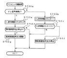
図51は、遊技機の電源断時の電源低下やNMI割込信号(ここでは、電源断信号)の様子を示すタイミング図である。遊技機に対する電力供給が断たれると、最も高い直流電源電圧であるVSLの電圧値は徐々に低下する。そして、この例では、+22Vにまで低下すると、電源基板910に搭載されている電源監視用IC902から電源断信号(電圧低下信号)が出力される(ローレベルになる)。
【0269】
電源断信号は、電気部品制御基板(図51に示す例では主基板31および払出制御基板37)に導入され、CPU56および払出制御用CPU371のNMI端子に入力される。CPU56および払出制御用CPU371は、上述したNMI処理によって、所定の電力供給停止時処理を実行する。
【0270】
VSLの電圧値がさらに低下して所定値(この例では+9V)にまで低下すると、主基板31や払出制御基板37に搭載されているリセットIC651の出力がローレベルになり、CPU56および払出制御用CPU371がシステムリセット状態になる。なお、CPU56および払出制御用CPU371は、システムリセット状態とされる前に、電力供給停止時処理を完了している。
【0271】
VSLの電圧値がさらに低下してVcc(各種回路を駆動するための+5V)を生成することが可能な電圧を下回ると、各基板において各回路が動作できない状態となる。しかし、少なくとも主基板31や払出制御基板37では、電力供給停止時処理が実行され、CPU56および払出制御用CPU371がシステムリセット状態とされている。
【0272】
リセットIC976が電源断を検知するための所定値は、通常時の電圧より低いが、払出制御用CPU371が暫くの間動作し得る程度の電圧である。また、リセットIC976が、払出制御用CPU371が必要とする電圧(この例では+5V)よりも高い電圧を監視するように構成されているので、払出制御用CPU371が必要とする電圧に対して監視範囲を広げることができる。従って、より精密な監視を行うことができる。
【0273】
また、この実施の形態では、電源基板910に搭載されている電源監視回路が、遊技機で使用される直流電圧のうちで最も高い電源VSLの電圧を監視して、その電源の電圧が所定値を下回ったら電圧低下信号(電源断検出信号)を発生する。図51に示すように、電源断検出信号が出力されるタイミングでは、IC駆動電圧は、まだ各種回路素子を十分駆動できる電圧値になっている。従って、IC駆動電圧で動作する払出制御基板37の払出制御用CPU371が所定の電力供給停止時処理を行うための動作時間が確保されている。
【0274】
なお、ここでも、電源監視回路は、遊技機で使用される直流電圧のうちで最も高い電源VSLの電圧を監視することになるが、電源断検出信号を発生するタイミングが、IC駆動電圧で動作する電気部品制御手段が所定の電力供給停止時処理を行うための動作時間が確保されるようなタイミングであれば、監視対象電圧は、最も高い電源VSLの電圧でなくてもよい。すなわち、少なくともIC駆動電圧よりも高い電圧を監視すれば、電気部品制御手段が所定の電力供給停止時処理を行うための動作時間が確保されるようなタイミングで電源断検出信号を発生することができる。
【0275】
この場合、上述したように、監視対象電圧は、賞球カウントスイッチ301A等の遊技機の各種スイッチに供給される電圧が+12Vであることから、電源断時のスイッチオン誤検出の防止も期待できる電圧であることが好ましい。すなわち、スイッチに供給される電圧(スイッチ電圧)である+12V電源電圧が落ち始める以前の段階で、電圧低下を検出できることが好ましい。よって、少なくともスイッチ電圧よりも高い電圧を監視することが好ましい。
【0276】
ただし、監視範囲が狭まるが、電圧監視回路および他の電圧監視回路の監視電圧として+5V電源電圧を用いることも可能である。その場合にも、電圧監視回路の検出電位は、他の電圧監視回路の検出電位よりも高く設定される。
【0277】
以上説明したように、電源断処理の際に電気部品制御手段がクリア信号を出力する構成としたことで、電源断状態となる前に電源断処理の際に出力ポートをクリアすることができるため、電源断状態となる前に各電気部品制御手段により制御される各電気部品を、適切な動作停止状態とすることができる。例えば、開放中の大入賞口を閉成させ、また開放中の可変入賞球装置15を閉成させ、さらには駆動状態にある払出モータ289の作動を停止させるなど、電気部品についての作動を停止させたあとに電源断状態とすることができる。従って、適切な停止状態で電源復旧を待機することが可能となる。
【0278】
また、上述したように、電源断処理の際に電気部品制御手段がクリア信号を出力する構成としたことで、主基板31は電断処理を実行し待機状態となっているにもかかわらず、払出制御基板37などの他の電気部品制御基板は電源が断たれずに復帰したような場合であっても、出力ポート57をクリアすることができるため、各電気部品制御手段により制御される各電気部品や各電気部品制御手段の動作状態などを適切な動作停止状態とすることができ、主基板31が待機状態となっているにもかかわらず各電気部品制御手段が制御動作を継続してしまうなどの誤動作を防止することができる。
【0279】
すなわち、例えば、主基板31が、待機状態となる直前に他の電気部品制御基板に対する制御コマンドの出力中であったとしても、主基板31が遊技制御を中断しているにもかかわらず、他の電気部品制御基板(例えば、表示制御基板80、音制御基板70、ランプ制御基板35)が演出を継続してしまうなどの誤動作を防止することができる。また、例えば、主基板31が待機状態となる直前に、大入賞口または可変入賞球装置15が開放中であったとしても、大入賞口および可変入賞球装置15が開放状態のままとされるようなことを防止することもできる。さらに、例えば、主基板31が、待機状態となる直前に管理コンピュータに対して情報を出力中であったとしても、誤った情報を出力してしまうようなことを防止することができる。
【0280】
また、上述したように、電源断処理の際に電気部品制御手段がクリア信号を出力する構成としたことで、払出制御基板37は電断処理を実行し待機状態となっているにもかかわらず、電気部品(例えば払出モータ289)などの所定の各部の電源が断たれずに復帰したような場合であっても、出力ポート372c,372e,372f,372gをクリアすることができるため、所定の各部の動作状態などを適切な動作停止状態とすることができ、払出制御基板37が待機状態となっているにもかかわらず電気部品などの所定の各部が制御動作を継続してしまうなどの誤動作を防止することができる。
【0281】
すなわち、例えば、払出制御基板37が待機状態となる直前に管理コンピュータに対して情報を出力中であったとしても、誤った球貸し情報を出力し続けてしまうことを防止することができる。また、例えば、払出モータ289の駆動状態を継続してしまうなどの誤動作や、エラー表示用LED374に誤ったエラー表示がされることを防止することもできる。さらに、例えば、払出制御基板37が待機状態であるにもかかわらず、カードユニット50に信号(例えば、EXS信号、PRDY信号)を誤って出力してしまうことや、振分ソレノイドに対する不適切な制御を行ってしまうことを防止することができる。
【0282】
なお、上述した各実施の形態では、電源監視手段は、電源基板および電気部品制御基板のいずれかに設置されたが、どこに設置されていてもよく、遊技機の構造上の都合等に応じて任意の位置に設置することができる。
【0283】
そして、上記の各実施の形態では、記憶手段としてRAMを用いた場合を示したが、記憶手段として、電気的に書き換えが可能な記憶手段であればRAM以外のものを用いてもよい。
【0284】
また、上述した各実施の形態では、遊技制御手段以外の他の電気部品制御手段として払出制御手段を例示したが、表示制御手段、音制御手段およびランプ制御手段についても、上述した制御を行うように構成し、停電発生NMI処理においてクリア信号を出力して、それぞれの電気部品制御手段が制御する電気部品の作動を停止するようにしてもよい。このように構成すれば、停止状態となる前に各電気部品の作動を停止状態にすることができ、適切な停止状態で電源復旧を待機することができる。また、各電気部品制御手段が待機状態となったにもかかわらず、それぞれの電気部品制御手段が制御する電気部品などの電源が断たれずに復旧した場合であっても、誤った演出の継続を中断することができる。例えば、ランプ制御手段であれば、始動記憶表示器18の点灯を誤って継続してしまうことを防止することができる。
【0285】
また、上記の実施の形態では、電源監視回路は電源基板910に設けられたが、電源監視回路は主基板31や払出制御基板37などの電気部品制御基板に設けられていてもよい。なお、電源回路が搭載された電気部品制御基板が構成される場合には、電源基板には、電源監視回路は搭載されない。
【0286】
上記の各実施の形態のパチンコ遊技機1は、始動入賞にもとづいて可変表示部9に可変表示される特別図柄の停止図柄が所定の図柄の組み合わせになると所定の遊技価値が遊技者に付与可能になる第1種パチンコ遊技機であったが、始動入賞にもとづいて開放する電動役物の所定領域への入賞があると所定の遊技価値が遊技者に付与可能になる第2種パチンコ遊技機や、始動入賞にもとづいて可変表示される図柄の停止図柄が所定の図柄の組み合わせになると開放する所定の電動役物への入賞があると所定の権利が発生または継続する第3種パチンコ遊技機であっても、本発明を適用できる。
【0287】
さらに、パチンコ遊技機に限られず、スロット機等においても、何らかの動作をする電気部品が備えられている場合などには本発明を適用することができる。
【0288】
【発明の効果】
以上のように、本発明によれば、遊技機を、マイクロコンピュータが搭載された制御基板には、マイクロコンピュータが電気部品の制御にかかわる指令信号を出力するための出力ポートが設けられ、マイクロコンピュータは、第1の電源監視手段からの検出信号により記憶手段の記憶内容が正常であるか否かを診断するためのチェックデータを生成して当該記憶手段に保存する処理を含む電力供給停止時処理を実行する電力供給停止時処理実行手段と、電力供給停止時処理にて前記電気部品の作動を停止させるためのクリア信号を出力して、クリア信号にもとづいて出力ポートをオフ状態とするクリア手段と、を有し、第2の電源監視手段からのシステムリセット信号に応じて非動作状態とされ、第2の電源監視手段は、監視する直流電圧が前記第1の電源監視手段が検出信号を出力したあと第2の電源監視手段がシステムリセット信号を出力するまでの所定期間内に、電力供給停止時処理実行手段により電力供給停止時処理が完了するように設定された検出電圧に低下したときに第2の条件が成立したとしてシステムリセット信号を出力する構成としたので、クリア信号によって停止状態となる前に電気部品の作動を停止させることができ、マイクロコンピュータに制御される電気部品を適切な状態として電源断状態とすることができるため、適切な停止状態で電源復旧を待機することができる。また、停止状態となる前に出力ポートがクリアされることにより、停止状態となる前に電気部品の作動を停止させることができ、マイクロコンピュータに制御される電気部品を適切な状態として電源断状態とすることができるため、適切な停止状態で電源復旧を待機することができる。また、所定の電力供給停止時処理を確実に実行することができる。従って、電力供給停止時処理の実行の際のクリア信号出力を確実に行うことができる。さらに、第1の電源監視手段による検出信号出力のあとに第2の条件が成立するように調整することにより、電力供給停止時処理の完了後にシステムリセットされるよう構成することができるため、電源断状態となる前に電力供給停止時処理を確実に完了させることができる。従って、電源断状態となる前に、確実に電気部品の作動を停止させることができる。また、早期に電源電圧の低下を検出することができるため、電源電圧の低下にもとづく電力供給停止時処理などの対応を迅速にとることができる。さらに、電力供給停止時処理の完了後にシステムリセット信号を出力することができるため、電源断状態となる前に、電力供給停止時処理を確実に完了させることができる。従って、電源断状態となる前に、確実に電気部品の作動を停止させることができる。
【0290】
遊技機は遊技者が所定の遊技を行った結果が所定の態様となった場合に遊技者に有利な特定遊技状態に制御可能であって、マイクロコンピュータが特定遊技状態で開閉される大入賞口の開放を指示する指令信号を出力し大入賞口がクリア信号によって閉状態とされるように構成されている場合には、停止状態となる前に開放状態にある大入賞口を閉成させることができ、大入賞口が開放状態とされたまま電源断状態とされることを回避することができるため、適切な停止状態で電源復旧を待機することができる。
【0294】
第1の電源監視手段が、マイクロコンピュータが搭載された制御基板とは別個に設けられた電源基板に搭載され、第2の電源監視手段が、制御基板に搭載されているとした場合には、電源監視手段による検出信号を各制御基板にてそれぞれ取り込むことあできるため、1つの電源監視手段からの検出信号を各制御基板でそれぞれ利用することができる。すなわち、簡単な構成で電源の監視を行うことができる。
【0296】
マイクロコンピュータが、電力供給停止時処理においてバックアップ記憶が格納されている領域へのアクセスを禁止する処理を実行するとした場合には、電源電圧が低下していくことに伴って生ずる可能性がある異常動作に起因するバックアップ記憶が格納されている領域(例えば、RAM)の内容破壊等を確実に防止することができ、その後の電源投入時に復旧されるRAMの保存データを確実に保護することができる。
【図面の簡単な説明】
【図1】パチンコ遊技機を正面からみた正面図である。
【図2】パチンコ遊技機の遊技盤を正面からみた正面図である。
【図3】パチンコ遊技機の機構板を背面からみた背面図である。
【図4】遊技制御基板(主基板)の回路構成例を示すブロック図である。
【図5】払出制御基板の回路構成例を示すブロック図である。
【図6】電源監視および電源バックアップのためのCPU周りの一構成例を示すブロック図である。
【図7】電源基板の一構成例を示すブロック図である。
【図8】主基板におけるCPUが実行するメイン処理の例を示すフローチャートである。
【図9】遊技状態復旧処理を実行するか否かの決定方法の例を示す説明図である。
【図10】初期化処理の例を示すフローチャートである。
【図11】2msタイマ割込処理の例を示すフローチャートである。
【図12】初期設定処理の例を示すフローチャートである。
【図13】遊技制御処理の例を示すフローチャートである。
【図14】各乱数を示す説明図である。
【図15】打球が始動入賞口に入賞したことを判定する処理を示すフローチャートである。
【図16】可変表示の停止図柄を決定する処理およびリーチ種類を決定する処理を示すフローチャートである。
【図17】大当り判定の処理を示すフローチャートである。
【図18】特別図柄プロセス処理を示すフローチャートである。
【図19】普通図柄プロセス処理を示すフローチャートである。
【図20】ゲートスイッチ処理を示すフローチャートである。
【図21】普通図柄に関する当り判定用乱数の当たり/はずれを示す説明図である。
【図22】普通図柄判定処理を示すフローチャートである。
【図23】普通図柄変動処理を示すフローチャートである。
【図24】普通図柄停止処理を示すフローチャートである。
【図25】停電発生NMI処理の例を示すフローチャートである。
【図26】バックアップパリティデータ作成方法の例を説明するための説明図である。
【図27】遊技状態復旧処理の例を示すフローチャートである。
【図28】払出制御コマンドのコマンド形態の一例を示す説明図である。
【図29】払出制御コマンドの内容の一例を示す説明図である。
【図30】払出制御コマンドの送出形態の他の例を示すタイミング図である。
【図31】払出制御コマンドの送出形態の一例を示すタイミング図である。
【図32】電源監視および電源バックアップのための払出制御用CPU周りの一構成例を示すブロック図である。
【図33】払出制御用CPUが実行するメイン処理の例を示すフローチャートである。
【図34】払出制御用CPUの初期設定処理の一例を示すフローチャートである。
【図35】払出制御用CPUの初期化処理の一例を示すフローチャートである。
【図36】払出制御用CPUのタイマ割込処理の例を示すフローチャートである。
【図37】払出制御手段におけるRAMの一構成例を示す説明図である。
【図38】払出制御用CPUのコマンド受信処理の例を示すフローチャートである。
【図39】払出制御用CPUが実行する払出制御処理の例を示すフローチャートである。
【図40】スイッチ処理の例を示すフローチャートである。
【図41】コマンド解析実行処理の例を示すフローチャートである。
【図42】払出停止状態設定処理の例を示すフローチャートである。
【図43】プリペイドカードユニット制御処理の例を示すフローチャートである。
【図44】球貸し制御処理の例を示すフローチャートである。
【図45】球貸し制御処理の例を示すフローチャートである。
【図46】賞球制御処理の例を示すフローチャートである。
【図47】賞球制御処理の例を示すフローチャートである。
【図48】払出制御用CPUが実行する停電発生NMI処理の例を示すフローチャートである。
【図49】バックアップパリティデータ作成方法の例を説明するための説明図である。
【図50】払出制御用CPUが実行する払出状態復旧処理の例を示すフローチャートである。
【図51】遊技機の電源断時の電源低下やNMI信号の様子の例を示すタイミング図である。
【符号の説明】
1 パチンコ遊技機
31 主基板
37 払出制御基板
372c,372e,372f,372g 出力ポート(I/Oポートの出力部)
53 基本回路
56 CPU
577,578 出力ポート(I/Oポートの出力部)
371 払出制御用CPU
651,976 リセットIC
902 電源監視用IC
910 電源基板[0001]
TECHNICAL FIELD OF THE INVENTION
The present invention relates to a gaming machine such as a pachinko gaming machine, a coin gaming machine, a slot machine, and the like in which a game is performed according to a player's operation, and in particular, a game is performed according to a player's operation in a gaming area of a gaming board. Related to gaming machines.
[0002]
[Prior art]
As a gaming machine, a game medium such as a game ball is launched into a game area by a launching device, and when a game medium wins a winning area such as a winning opening provided in the game area, a predetermined number of prize balls are paid out to the player. There are things to be done. Further, a variable display unit whose display state can be changed is provided, and when a display result of the variable display unit becomes a predetermined specific display mode, a predetermined game value is provided to the player. There is.
[0003]
In addition, the game value is a right to make the state of the variable prize ball device provided in the game area of the gaming machine advantageous for a player who is easy to win a hit ball, or to a state advantageous to the player. Or that the condition for prize game medium payout becomes easy to be satisfied. Also, the addition of a predetermined amount of game balls or coins or the addition of points is also included in the game value.
[0004]
In a pachinko gaming machine, when a display result of a variable display unit that displays a special symbol is a combination of a predetermined specific display mode, it is generally referred to as a “big hit”. When a big hit occurs, for example, the big winning opening is opened a predetermined number of times, and the state shifts to a big hit game state in which a hit ball is easy to win. Then, in each open period, when a predetermined number (for example, 10) of the winning prizes is won, the winning prize opening is closed. The number of opening of the special winning opening is fixed to a predetermined number (for example, 16 rounds). An opening time (for example, 29.5 seconds) is determined for each opening, and if the opening time elapses even if the number of winnings does not reach a predetermined number, the winning opening is closed. If the predetermined condition (for example, winning in the V zone provided in the special winning opening) is not satisfied at the time when the special winning opening is closed, the big hit gaming state ends.
[0005]
Further, among the combinations of display modes other than the combination of “big hits”, when a part of the display results of the plurality of variable display units is not yet derived and displayed, the final or temporary display result is already displayed. Is referred to as “reach” when the display mode of the variable display unit on which the display mode is displayed satisfies the display condition that is a combination of the specific display modes. If the display result of the identification information variably displayed on the variable display unit does not satisfy the condition of "big hit", the result is "miss" and the variable display state ends. A player plays a game while enjoying how to generate a big hit.
[0006]
When a game ball wins a winning opening provided on the game board, a predetermined number of payout balls are paid out. Since the progress of the game is controlled by the game control means mounted on the main board, the number of winning balls based on the winning is determined by the game control means and transmitted to the payout control board. Hereinafter, the game control means and the other control means may be respectively referred to as electric component control means.
[0007]
[Problems to be solved by the invention]
As described above, the gaming machine is equipped with various electric component control means including the game control means. Generally, each electric component control means is constituted by a microcomputer, and after a power failure occurs, the control is returned from the initial state, so that a problem that the player cannot receive the profit that should have been obtained may occur. As one of means for solving such a problem, the game control is interrupted in response to a predetermined signal issued along with a decrease in the voltage value of the gaming machine due to a power failure or the like, and the power cutoff process is started, and the power cutoff state is set. There is a method in which the stored contents are protected by a backup power supply and the power supply is restored.
[0008]
In the case where such a method is used, for example, if the power-off processing is performed while each electric component control unit is operating, the power is turned off during the operation of each electric component control unit. There has been a problem that an electric component operated under the control of the electric component control means cannot wait for recovery from a power failure or the like in an appropriate operation stop state.
[0009]
In view of the above, the present invention provides a gaming machine capable of setting an electric component controlled by each electric component control unit to an appropriate operation stop state at the time of power supply cutoff processing and waiting for power restoration in an appropriate stop state. The purpose is to do.
[0010]
[Means for Solving the Problems]
A gaming machine according to the present invention is a gaming machine in which a player plays a predetermined game and pays out a prize ball to the player in response to a game ball winning a prize area provided in the game area. Microcomputer which performs control processing for controlling electric components (large winning opening, variable winning
[0012]
The gaming machine can be controlled to a specific gaming state advantageous to the player when the result of the player performing the predetermined game becomes a predetermined mode, Microcomputer May output a command signal instructing opening of a special winning opening that is opened and closed in a specific game state, and the special winning opening may be configured to be closed by a clear signal.
[0016]
The first power monitoring means is Microcomputer Was installed Control board Is mounted on a power supply board provided separately from the power supply board. Control board May be configured to be mounted on a computer.
[0018]
Microcomputer May be configured to execute processing for prohibiting access to the area where the backup storage is stored in the power supply stop processing.
Characterized by
[0019]
BEST MODE FOR CARRYING OUT THE INVENTION
Hereinafter, an embodiment of the present invention will be described with reference to the drawings.
First, the overall configuration of a pachinko gaming machine, which is an example of a gaming machine, will be described. 1 is a front view of the
[0020]
As shown in FIG. 1, the
[0021]
Near the center of the
[0022]
An opening / closing plate 20 that is opened by the solenoid 21 in a specific game state (big hit state) is provided below the variable winning
[0023]
The
[0024]
In this example, a
[0025]
The
[0026]
The hit ball fired from the hitting ball launching device enters the
[0027]
The rotation of the image in the
[0028]
If the combination of images in the
[0029]
Next, the structure of the back surface of the
On the back side of the
[0030]
On the
[0031]
FIG. 3 is a rear view of the mechanical plate of the
[0032]
To perform the prize ball payout control, signals from the winning
[0033]
FIG. 4 is a block diagram illustrating an example of a circuit configuration of the
[0034]
Also, according to the data provided from the
[0035]
The
[0036]
Further, the
[0037]
A hit ball launching device that hits and launches a game ball is driven by a
[0038]
In this embodiment, the lamp control means mounted on the
[0039]
FIG. 5 is a block diagram showing components related to payout, such as components of the
[0040]
The detection signal from the ball out switch 187 (187a, 187b) is input to the I /
[0041]
The
[0042]
Further, a detection signal from the award
[0043]
When there is a prize, a payout control command indicating the number of prize balls is input to the
In this embodiment, the
[0044]
The
[0045]
Further, detection signals from the prize
[0046]
The
[0047]
A ball lending switch signal and a return switch signal are given from the
[0048]
When the power of the
[0049]
As described above, all signals from the
[0050]
In this embodiment, the case where the
[0051]
In this embodiment, the RAM in the
[0052]
FIG. 6 is a block diagram showing a configuration example around the
[0053]
FIG. 6 also shows a
[0054]
As shown in FIG. 6, the reset signal from the
[0055]
Then, for example, the detection voltage of the first power supply monitoring circuit (the voltage at which a voltage drop signal is output) is set to +22 V, and the detection voltage of the second power supply monitoring circuit is set to +9 V. In such a configuration, since the first power supply monitoring circuit and the second power supply monitoring circuit monitor the voltage of the same power supply VSL, the timing at which the first voltage monitoring circuit outputs the voltage drop signal And the timing at which the second voltage monitoring circuit outputs the voltage drop signal can be reliably set to a desired predetermined period. The desired predetermined period is a period from when the power supply stop processing is started in response to the voltage drop signal from the first power supply monitoring circuit to when the power supply stop processing is surely completed.
[0056]
In this example, the first detection condition under which the first power supply monitoring means outputs a detection signal is that the +30 V power supply voltage has dropped to +22 V, and the second power supply monitoring means outputs the detection signal. The second detection condition becomes that the +30 V power supply voltage has dropped to +9 V. However, the voltage value used here is an example, and another value may be used.
[0057]
However, although the monitoring range is narrowed, it is also possible to use a + 5V power supply voltage as the monitoring voltage of the first voltage monitoring circuit and the second voltage monitoring circuit. Also in that case, the detection voltage of the first voltage monitoring circuit is set higher than the detection voltage of the second voltage monitoring circuit.
[0058]
While power is not supplied from the +5 V power supply, which is the driving power supply of the
[0059]
Although FIG. 6 shows a configuration in which two reset signals (low level signals) are supplied to the reset terminal of the
[0060]
FIG. 7 is a block diagram illustrating a configuration example of a
[0061]
Transformer 911 converts an AC voltage from an AC power supply to 24V. The AC 24 V voltage is output to connector 915. The
[0062]
The + 5V line from DC-DC converter 913 branches to form a backup + 5V line. A large-capacity capacitor 916 is connected between the backup + 5V line and the ground level. The capacitor 916 is provided with a power so as to maintain a storage state in a backup RAM (power-backed-up RAM, that is, storage means that can be in a storage content storage state) of the electric component control board when power supply to the gaming machine is cut off. Supply backup power. Further, a
[0063]
Note that a battery that can be charged from a + 5V power supply may be used as the backup power supply. In the case of using a battery, a rechargeable battery is used which runs out of capacity when power is not supplied from a + 5V power supply for a predetermined time.
[0064]
The
[0065]
The predetermined value for the power
[0066]
Further, since the power
[0067]
In the configuration shown in FIG. 7, the detection output (voltage drop signal) of the power
[0068]
Next, the operation of the gaming machine will be described.
FIG. 8 is a flowchart illustrating a main process executed by the
[0069]
Then, it is confirmed whether or not the data protection processing of the backup RAM area (NMI processing of power failure occurrence such as addition of parity data in this example) is performed when the power is turned off (step S2). When an unexpected power failure occurs, a process for protecting data in the backup RAM area is performed as described later. The case where such protection processing has been performed is regarded as backup. If it is determined that there is no backup, an initialization process is performed (steps S2 and S3). In this example, whether or not there is backup data in the backup RAM area is confirmed by the state of the backup flag set in the backup RAM area when the power is turned off. In this example, if "55H" is set in the backup flag area, it means that there is a backup (ON state), and if a value other than "55H" is set, it means that there is no backup (OFF state).
[0070]
If there is backup data in the backup RAM area, in this embodiment, the
[0071]
If the check result is normal, the
[0072]
After the execution of the normal initialization process (steps S2 and S3), the main process executed by the
[0073]
In this embodiment, after checking the presence or absence of backup data in step S2, if backup data exists, the backup area is checked in step S4. After confirming that the backup data is normal, the presence or absence of backup data may be confirmed. In addition, a configuration may be adopted in which it is determined whether to execute the power failure recovery process by confirming whether there is backup data or checking the backup area.
[0074]
Further, for example, at the time of the parity check (step S4) when determining whether or not to execute the power failure recovery processing, that is, at the time of determining whether or not to restore the gaming state, a special process in the stored RAM data is performed. If it is confirmed that the gaming machine is in a game waiting state (a state in which no symbol is changing, no big hit game is in progress, and there is no start winning prize memory) by a flag or the like or the data of the number of start winning prizes. Alternatively, the initialization process may be performed without performing the game state restoration process.
[0075]
In the normal initialization process, as shown in FIG. 10, the RAM is cleared (step S3a). Then, based on the address value of the work area initial setting table, a predetermined work area (for example, a normal symbol determination random number counter, a normal symbol determination buffer, a special symbol left middle right symbol buffer, a payout command storage pointer, etc.) is initialized. An initial value setting process for setting a value (step S3b) is performed. Then, the timer register provided in the
[0076]
Therefore, in this embodiment, the internal timer of the
[0077]
When detecting that the timer interrupt flag is set in step S9, the
[0078]
As described above, in this embodiment, it is determined whether or not the power is restored to the state at the time of the power failure based on the presence or absence of the backup data. Therefore, when the power is turned on, for example, when the power is restored after a power failure, it is possible to determine whether or not to restore the state at the time of the power failure according to the contents of the backup data storage area.
[0079]
Further, as described above, since it is determined whether or not the power is restored to the power-off state based on the state of the backup data, the backup data storage is performed when the power is turned on when the power is restored after a power failure. It is possible to determine whether or not to restore the power-off state according to the state of the contents of the area.
[0080]
FIG. 12 is a flowchart showing the initial setting process in step S1. In the initial setting process, the
[0081]
Note that there are the following three types of maskable interrupt interrupt modes in which an interrupt is permitted by inputting an INT signal that can be set in the initial setting process.
Interrupt mode 0: The built-in device that has issued the interrupt request sends an RST instruction (1 byte) or a CALL instruction (3 bytes) onto the internal data bus of the CPU. Therefore, the
Interrupt mode 1: A mode in which the start address (38 (H)) of the interrupt processing program is determined in advance.
Interrupt mode 2: In this mode, an address synthesized from the value (1 byte) of a specific register of the
[0082]
FIG. 13 is a flowchart showing the game control processing in step S11. In the game control process, first, the
[0083]
Next, various abnormality diagnosis processes are performed by the self-diagnosis function provided inside the
[0084]
Next, a process of updating each counter indicating a random number for determination, such as a random number for big hit determination, used for game control is performed (step S23). The
[0085]
Further, the
[0086]
The
[0087]
Next, the
[0088]
Further, the
[0089]
The
[0090]
As described above, the main process includes the process of determining whether or not to shift to the game control process, and the internal timer of the
[0091]
In a conventional general game control process, an external interrupt that is periodically generated forcibly returns to an initial state. Describing with reference to the example shown in FIG. 13, for example, even during the process of step S31, the process is forcibly returned to the process of step S21. In other words, there is a possibility that the next game control process will be started before all the processes in the game control process are completed.
[0092]
Here, the game control process executed by the
[0093]
Even in such a configuration, the flag is not determined until all the game control processes are executed, so that execution of all the processes in the game control process is guaranteed to be completed.
[0094]
FIG. 14 is an explanatory diagram showing random numbers such as a jackpot determining random number used for game control. Each random number is used as follows.
(1) Random 1: Determine whether to generate a big hit (for big hit determination)
(2) Random 2-1 to 2-3: For determining the left and right middle out-of-designs
(3) Random 3: Determine the combination of symbols at the time of the big hit (for big hit symbol determination)
(4) Random 4: Determine whether or not to make a probability change jackpot (for probability change determination)
(5) Random 5: Determine whether to reach at the time of off (for reach judgment)
(6) Random 6: Determine reach type (for determining reach type)
(7) Random 7: Determines whether or not to make a hit with a normal symbol (for hit judgment)
[0095]
In addition, random numbers other than the above-mentioned random numbers (1) to (7) are used to enhance the game effect.
In step S23, the
[0096]
Next, a method of determining a symbol (special symbol) variably displayed on the
[0097]
When the hit ball wins the starting winning port 14 provided in the
[0098]
As shown in FIG. 16, the
[0099]
Then, the
[0100]
When it is determined that the jackpot is a big hit, the
[0101]
If it is determined that there is a loss, the
[0102]
In this embodiment, the left and right symbols are determined according to the value of the random 2-1 (step S91). Also, the middle symbol is determined according to the value of the random 2-2 (step S92). That is, one of the symbols corresponding to the values of 0 to 15 of the values of the random 2-1 and the random 2-2 is determined as the stop symbol. Here, when the determined middle symbol matches the left and right symbols, the symbol corresponding to the value obtained by adding 1 to the value of the random number corresponding to the middle symbol is determined as the symbol of the middle symbol so that it does not match the big hit symbol. I do.
[0103]
Further, the
[0104]
As described above, it is determined whether the display mode of the symbol variation based on the winning start is a big hit, a reach mode, or a loss, and the combination of the respective stop symbols is determined.
[0105]
In the high-probability state, the probability of the next big hit increases, the time required to determine the variable display of the
[0106]
The range of the random numbers and the random number values used in this embodiment is an example, and any random numbers may be used, and the range setting is arbitrary.
[0107]
FIG. 18 is a flowchart showing an example of a special symbol process program executed by the
[0108]
In the variation shortening timer subtraction process in step S310, it is determined whether or not a condition for shortening the variation time of the special symbol is satisfied (for example, a predetermined time elapses from the start winning detection to the execution of the process based on the starting winning). Is performed, a process of decrementing a fluctuation shortening timer for confirming whether or not the timer has been performed is performed. Then, in each processing of steps S300 to S309, the following processing is executed.
[0109]
Special symbol change waiting process (step S300): The start winning port 14 (in this embodiment, the winning port of the variable winning ball device 15) is hit and the starting
Special symbol determination processing (step S301): When a state in which the variable display of the special symbol can be started, the number of stored start winnings is confirmed. If the number of start winning prizes is not 0, it is determined whether to make a jackpot or not according to the value of the extracted jackpot determination random number. That is, the first half of the processing shown in FIG. 16 is executed.
Stop symbol setting process (step S302): A stop symbol for the left and right middle symbols is determined. That is, the middle half of the processing shown in FIG. 16 is executed.
[0110]
Reach operation setting process (step S303): Determine whether or not to perform the reach operation according to the value of the reach determination random number, and determine the fluctuation period during reach according to the value of the reach type determination random number. That is, the latter half of the process shown in FIG. 16 is executed.
[0111]
All symbols change start process (step S304): Control is performed so that all symbols start to change in the
[0112]
All symbols stop waiting process (step S305): When a predetermined time (time indicated by the variation reduction timer in step S310) has elapsed, control is performed so that all symbols displayed on the
[0113]
Big winning opening opening process (step S306): Control for opening the big winning opening is started. Specifically, the counter and the flag are initialized, and the solenoid 21 is driven to open the special winning opening. Also, a big hit flag (a flag indicating that a big hit is being made) is set. Upon completion of the process, the internal state (process flag) is updated so as to shift to step S307.
[0114]
Processing during opening of the special winning opening (step S307): Control for transmitting display control command data of the special winning opening round display to the
[0115]
Specific area effective time processing (step S308): The presence or absence of the passage of the
[0116]
Big hit end processing (step S309): A display for notifying the player that the big hit gaming state has ended is performed. When the display is completed, the internal state is updated so as to shift to step S300.
[0117]
As described above, when a hit ball is won in the starting winning opening 14, the
[0118]
FIG. 19 is a flowchart showing the ordinary symbol processing (step S26). In the ordinary symbol process process, the
[0119]
As shown in FIG. 20, in the gate switch processing, the turning on of the
[0120]
In the normal symbol change waiting process of step S62, if the value of the normal symbol passage storage counter is other than 0, the
[0121]
FIG. 21 is an explanatory diagram showing the relationship between the hit determination random number (random 7) and the hit / miss in this embodiment. As shown in FIG. 21, when the probability is high, the hit value is one of 3 to 12, and when the probability is low, it is 3, 5 or 7. If the value of the random number for hit determination matches the hit value, the hit is determined. In addition, the time of the high probability of the normal symbol coincides with the time of the probability change, for example.
[0122]
FIG. 22 is a flowchart showing the ordinary symbol determination processing in step S63. In the ordinary symbol determination processing, the
[0123]
Then, the
[0124]
In addition, in order to notify the
[0125]
Then, a normal symbol variation time timer is started (step S637). For example, at the time of a high probability, a value equivalent to 5.1 seconds is set in the normal symbol fluctuation time timer. At the time of the low probability, a value equivalent to 29.2 seconds is set to the normal symbol fluctuation time timer. Further, the ordinary symbol process flag is updated to a value indicating the ordinary symbol variation process (step S638).
[0126]
The change control of the ordinary symbol in the
[0127]
In the ordinary symbol variation process of step S64, it is checked whether or not the ordinary symbol variation time timer has timed out, for example, as shown in FIG. 23 (step S641). If the timeout has occurred, the normal symbol process flag is updated to a value indicating the normal symbol stop processing (step S642).
[0128]
In the normal symbol stop process of step S65, control is performed to transmit a display control command indicating a normal symbol change stop, for example, as shown in FIG. 24 (step S651). Then, when it is determined to be a hit (step S652), the normal electric accessory hit flag is set (and the corresponding test signal is turned on), and the normal symbol process flag is set to start winning opening / closing processing. (Step S653). In the start winning opening opening / closing process, control is performed to open the starting winning opening (variable winning ball device 15) a predetermined number of times for a predetermined period. If it is determined to be a loss, the normal symbol process flag is updated to a value indicating the normal symbol change waiting process (step S654).
[0129]
The opening pattern used in the start winning opening opening / closing process is, for example, a pattern in which the variable winning
[0130]
FIG. 25 shows the voltage from the power supply monitoring circuit of the
Note that if a CPU having a specification that does not cause another interrupt during the interrupt process is used, the process of step S42 is unnecessary.
[0131]
Next, the
[0132]
First, the contents of each register are stored in the backup RAM area (step S44). Thereafter, a backup flag is set (step S45). Then, an appropriate initial value is set in the backup check data area of the backup RAM area (step S46), exclusive OR is sequentially performed on the initial value and the data of the backup RAM area, and the result is inverted (step S47). The calculated value is set in the backup parity data area (step S48). Further, the RAM access is prohibited (step S49). When the power supply voltage decreases, the levels of various signal lines may become unstable and the contents of the RAM may be corrupted. However, if the RAM access is prohibited in this manner, the data in the backup RAM may be corrupted. There is no.
[0133]
Further, the
[0134]
Next, the
[0135]
In this embodiment, in the power failure occurrence NMI process, the program is set in a loop state at the last part, but a HALT instruction may be issued.
[0136]
As described above, the backup flag set after storing the contents of the register in the RAM area determines whether there is backup data to be restored at power-on (whether restoration from a power failure or not). Used when Further, the processing of steps S41 to S50 is completed before the
[0137]
In this embodiment, the backup flag is confirmed at the time of starting the power supply stop processing. If the backup flag has already been set, the power supply stop processing is not executed. As described above, the backup flag is a flag indicating that the backup of necessary data has been completed and then the power supply stop processing has been completed. Therefore, for example, even if the NMI occurs again for some reason in the loop waiting for the reset, the power supply stop processing is not performed repeatedly.
[0138]
However, if a CPU having a specification that does not cause another interrupt during the interrupt processing is used, the determination in step S43 is unnecessary.
[0139]
FIG. 26 is an explanatory diagram for describing an example of a backup parity data creation method. However, in the example shown in FIG. 26, the size of the data in the backup data RAM area is 3 bytes for simplicity. In the power failure generation process based on the power supply voltage drop, as shown in FIG. 26, initial data (00H in this example) is set in the backup check data area. Next, an exclusive OR of “00H” and “F0H” is obtained, and an exclusive OR of the result and “16H” is obtained. Further, an exclusive OR of the result and “DFH” is obtained. Then, a value (“C6H” in this example) obtained by inverting the result (“39H” in this example) is set in the backup parity data area.
[0140]
When the power is turned on again, the parity diagnosis is performed in the power failure recovery processing. If all the data in the backup area is stored as it is, the data as shown in FIG. 26 is set in the backup area when the power is turned on again.
[0141]
In the processing of step S4, the
[0142]
Therefore, the
[0143]
As described above, in this embodiment, the game control means is provided with the storage means (backup RAM in this example) which is backed up for a predetermined period of time even when the power of the gaming machine is turned off. The CPU 56 (specifically, a program executed by the CPU 56) is configured to perform a game state restoration process (step S6) for restoring the game state based on the backup data when the storage unit is in the backup state.
[0144]
In this embodiment, the power supply monitoring circuit is mounted on the
[0145]
Then, the
[0146]
As described above, in this embodiment, the
[0147]
In this embodiment, the power
[0148]
In the above embodiment, the
[0149]
Further, when an interrupt signal from the power supply board is detected via the IRQ terminal instead of the NMI interrupt signal, an IRQ interrupt mask is set at the start of the game control process in step S11 of the main process, and the game control is performed. The IRQ interrupt mask may be released at the end of the processing. In such a case, an interruption occurs before and after the start of the game control process, so that the game control process is not interrupted halfway. Therefore, there is no possibility that the command transmission is interrupted when the payout control command is transmitted to the
[0150]
In this embodiment, in the power failure occurrence processing (power supply stop processing), if the backup flag indicating that the data has already been backed up and the power supply stop processing has already been executed is set, the power supply is stopped. It is configured not to execute the stop-time processing. In the process of turning off the power, NMI may occur again. Then, if the backup flag is not confirmed in the power failure occurrence processing, the power supply stop processing is executed again by the NMI that has occurred again.
[0151]
In the normal power supply stop processing executed first, processing for storing the contents of the register in the backup RAM is performed (see step S44 in FIG. 25). Since the power supply voltage gradually decreases in the state of waiting for reset after the normal power supply stop processing executed first, the contents of the register may be destroyed. That is, the register value may have changed from the state at the time when the power-off was detected (when the NMI first occurred). If the power supply stop processing is executed again in such a state, a value different from the register value in the state at the time when the power-off is detected is stored in the backup RAM. Then, in the power failure recovery processing executed at the time of power recovery, a value different from the register value in the state at the time when the power failure is detected is restored to the register. As a result, there is a possibility that a game state different from the game state when the power is turned off is reproduced.
[0152]
Hereinafter, the game state restoration processing will be described.
FIG. 27 is a flowchart illustrating an example of the gaming state restoring process shown in step S6 of FIG. In this example, the
[0153]
As described above, in the game state restoring process, the states of various electric components are restored according to the restored internal state, and the
[0154]
As a result, in this embodiment, the following state restoration can be performed by the game state restoration processing.
[0155]
The states of the start winning port 14 and the large winning port (opening / closing plate 20) are restored. The display state of the ordinary symbols (the display state of the variable display 10) controlled by the display control means is restored except for the case where the display is changing when the power is turned off. The display state of the special symbol controlled by the display control means (the display state of the variable display unit 9) is restored except for the case where it is changing when the power is turned off. Further, the background and the character displayed on the
[0156]
If the power is turned off during the change of the special symbol, information on the change time (for example, 10 seconds) of the variable display pattern and the time already executed (for example, 4 seconds) are backed up. Then, at the time of restoration, the
[0157]
In addition, when the power is turned off during the big hit game, the remaining time of the round or the interval between rounds is displayed at the time of restoration, as in the case of the power being turned off during the change of the special symbol described above, The
[0158]
The display states of the
[0159]
The sound generation state controlled by the voice control means is restored except during a special symbol change and a big hit game. However, if a big hit game is being played when the power is turned off, the initial state of each control section can be restored. When the power is turned off during the special symbol change and the power is restored, the sound generation state is controlled for the remaining time in the same manner as the display control of the
[0160]
In this embodiment, at the time of recovery from the power interruption, the control command for restoring the state is transmitted from the game control unit of the
[0161]
Further, as described later, the payout control means mounted on the
[0162]
When the game state is returned to the state at the time of power-off, in this embodiment, the
[0163]
Here, the game state restoring processing program is configured to return to the main processing when the game state restoring processing ends, but the stack area (backup RAM) pointed to by the stack pointer stored in the power supply interruption processing The address may be returned to the address stored in the area (in the area) (the address being executed when the NMI interrupt occurs when the power is turned off).
[0164]
As described above, after the initial setting process is started, until the recovery process is completed, or until the initialization process is completed, the process is interrupted by the interrupt prohibition state. Therefore, it is possible to reliably perform the initial setting, the determination as to whether or not to restore the state at the time of power interruption performed according to the contents of the backup data storage area, and the restoration processing (or initialization processing). Can be completed. Even in the case where the interrupt prohibition state is set before the end of the recovery processing as described above, the interrupt prohibition / permission state at the time of power-off is backed up by the parity flag. The interrupt prohibition / permission state when the power is turned off can be reliably restored.
[0165]
Note that, in the above embodiment, the case where the game control unit performs the data saving process and the restoration process has been described, but a part of the RAM in the payout control unit, the voice control unit, the ramp control unit, and the display control unit is also described. The power supply is backed up, and the payout control unit, the display control unit, the sound control unit, and the lamp control unit may also perform the processing described above. However, the payout control unit, the display control unit, the sound control unit, and the lamp control unit do not need to perform the command sending process at the time of restoration.
[0166]
FIG. 28 is an explanatory diagram illustrating an example of a command form of the payout control command. In this embodiment, the payout control command has a 2-byte configuration, the first byte represents MODE (command classification), and the second byte represents EXT (command type). The command form shown in FIG. 28 is an example, and another command form may be used.
[0167]
FIG. 29 is an explanatory diagram showing an example of the content of the payout control command. In the example shown in FIG. 29, the command FF00 (H) is a payout control command that specifies a payable state. The command FF01 (H) is a payout control command for specifying a payout stop state. The command F0XX (H) is a payout control command for specifying the number of winning balls. “XX” in the second byte indicates the number of payouts.
[0168]
The payout control means stops the prize ball payout and the ball lending when receiving the FF01 (H) payout control command from the game control means of the
[0169]
FIG. 30 is a timing chart showing an example of a delivery mode of the payout control command. In this embodiment, the payout control command has a 2-byte configuration. For example, as shown in FIG. 30, when the first and second bytes of the payout control signal are output, the INT signal is turned on. (Low level in this example). The ON period of the INT signal is, for example, 1 μs or more, and a period of, for example, 10 μs or more is provided between the first byte and the second byte. Note that the payout control command may have a one-byte configuration.
[0170]
The payout control command is sent only once so that the payout control means can recognize it. Recognizable means that the INT signal is turned on in this example, and is transmitted only once so that it can be recognized. In this example, it means that the INT signal is sent to the first and second bytes of the payout control signal. Accordingly, the INT signal is turned on only once.
[0171]
As shown in FIG. 31, the payout control command may have a one-byte configuration. In this case, a payout control command is output by 8-bit payout control signals CD to CD7. Then, when the payout control signal is being output, the INT signal is turned on (low level in this example). The ON period of the INT signal is, for example, 1 μs or more. The payout control means inputs the payout control signals CD to CD7 by an interrupt process according to the INT signal.
[0172]
Next, as an example of the case where the data saving and the clearing and restoring of the output port are performed in the electric component controlling means other than the game controlling means, the case where the data saving, the clearing of the output port and the restoring are performed in the payout controlling means explain.
FIG. 32 is a block diagram illustrating a configuration example around the
[0173]
The INT signal from the
[0174]
The
[0175]
The predetermined value for the
[0176]
While power is not supplied from the + 5V power supply, at least a part of the built-in RAM of the
[0177]
As described above, in this embodiment, the first power supply monitoring circuit mounted on the
[0178]
Note that, also in this case, the first power supply monitoring circuit monitors the highest voltage of the power supply VSL among the DC voltages used in the gaming machine. The monitoring target voltage does not need to be the highest voltage of the power supply VSL as long as the operation time for the electric component control means operating at the voltage to perform the predetermined power supply stop processing is secured. That is, if at least the voltage higher than the IC drive voltage is monitored, the power-off detection signal can be generated at a timing such that the operation time for the electric component control means to perform the predetermined power supply stop processing is secured. it can.
[0179]
In this case, as described above, since the voltage to be monitored is +12 V supplied to various switches of the gaming machine such as the prize
[0180]
In the configuration shown in FIG. 32, when the power is turned on, the system reset
[0181]
FIG. 33 is a flowchart showing the main processing of the
[0182]
FIG. 34 is a flowchart showing the initial setting process in step S701. In the initial setting process, the
[0183]
In this embodiment, an interrupt based on the count-up of CH2 and CH3 is used as a timer / counter interrupt. The interrupt based on the count-up of CH2 is an interrupt that occurs when the value of the timer counter register CLK / TRG2 becomes “0”. Therefore, in step S701e, the initial value “1” is set in the timer counter register CLK / TRG2. The interrupt based on the count-up of CH3 is an interrupt generated when the internal clock of the CPU counts down and the register value becomes "0", and is used as a 2 ms timer interrupt described later. Specifically, the register value of CH3 is subtracted in 1/256 cycle of the system clock. In step S701e, a value corresponding to 2 ms is set in the register of CH3 as an initial value. The interrupt address for CH2 is 0074H, and the interrupt address for CH3 is 0076H.
[0184]
Then, the
[0185]
If the backup data exists in the backup RAM area, in this embodiment, the
[0186]
If the check result is normal, the
[0187]
After the execution of the normal initialization process (step S703), the main process executed by the
[0188]
In this embodiment, after checking the presence or absence of backup data in step S702, if backup data exists, the backup area is checked in step S704. After confirming that the backup data is normal, the presence or absence of backup data may be confirmed. Further, it may be configured to determine whether or not to execute the power failure recovery process by confirming whether there is backup data or checking the backup area.
[0189]
Also, for example, at the time of a parity check (step S704) when determining whether or not to execute the power failure recovery processing, that is, when determining whether or not to restore the gaming state, the payout in the stored RAM data is performed. If it is confirmed from the game ball number data or the like that the gaming machine is in the payout standby state (not in the middle of payout), the initialization processing may be executed without performing the payout state restoration processing.
[0190]
In the normal initialization process, as shown in FIG. 35, a process of clearing the register and the RAM (step S901) is performed, and a predetermined initial value is set (step S902). Since the interrupt is prohibited in the initial setting process (step S701a), the interrupt is permitted before the initialization process is completed (step S903).
[0191]
In this embodiment, the internal timer (CH3) of the
[0192]
When detecting that the timer interrupt flag has been set in step S708, the
[0193]
When the power is turned on, the
[0194]
Further, in this example, the
[0195]
FIG. 37 is an explanatory diagram showing an example of use of the RAM incorporated in the
[0196]
FIG. 38 is a flowchart showing the payout control command receiving process by the interrupt process. The INT signal for payout control from the
[0197]
In the receiving process of the payout control command, the
[0198]
If it is not the first byte of the payout control command, it is checked whether the first byte has already been received (step S854). Whether or not the data has already been received can be confirmed based on whether or not valid data is set in the reception buffer (determination command buffer in step S853).
[0199]
If the first byte has already been received, it is checked whether the first bit of the received one byte is “0”. If the first bit is “0”, the valid second byte is received, and the received command is stored in the confirmed command buffer indicated by the command reception number counter + 1 in the confirmed command buffer area (step S855). The first bit should be “0” in the EXT byte (second byte) of the payout control command having a 2-byte configuration (see FIG. 28). Although not shown, if the first bit of the received one byte is not “0” in the confirmation after Y in step S854, the process ends.
[0200]
When the command data of the second byte is stored in step S855, 2 is added to the command reception number counter (step S856). Then, it is checked whether or not the command reception counter is 12 or more (step S857), and if it is 12, the command reception number counter is cleared (step S858).
[0201]
FIG. 39 is a flowchart showing the payout control processing in step S710. In the payout control processing, the
[0202]
Next, the
[0203]
Next, the
[0204]
Also, the
[0205]
In this embodiment, a stepping motor is used as the
[0206]
Next, error detection processing is performed, and a predetermined display is performed on the
[0207]
Prize ball path error: when the prize ball payout operation is completed, or when the prize
[0208]
Ball lending path error: when the ball lending payout operation is completed, or when the
[0209]
Prize ball count switch ball clogging error: when the prize
[0210]
Ball lending count switch ball clogging error: when the ball lending count switch 301B detects ON for 0.5 seconds or more. “3” is displayed on the
[0211]
Dispensing motor ball biting error: when dispensing
[0212]
Prepaid card unit non-connection error: when VL signal off is detected. “5” is displayed on the
[0213]
Prepaid card unit communication error: When it is detected that a signal is output from the
[0214]
Dispensing stop state: When a dispensing control command indicating dispensing stop is received from the
[0215]
Further, processing for controlling an information signal output from an external connection terminal (not shown) is performed (output processing: step S760). Note that the information signal is a signal that is turned on for a predetermined time for each unit (for example, 25 pieces) of loaned balls, and then is output for a predetermined time.
[0216]
FIG. 40 is a flowchart illustrating an example of the switch processing in step S751. In the switch processing, the
[0217]
Then, the value of the prize ball count switch on counter is checked (step S751c). If the value is 2, it is determined that one prize ball has been paid out. If it is determined that one prize ball has been paid out, the
[0218]
If it is confirmed in step S751a that the prize
[0219]
Then, the value of the ball lending count switch on counter is checked (step S751h). If the value is 2, it is determined that one lending ball has been paid out. When determining that one loaned ball has been paid out, the
[0220]
If it is confirmed in step S751f that the ball lending count switch 301B is not on, the
[0221]
FIG. 41 is a flowchart illustrating an example of the command analysis execution process in step S753. In the command analysis execution processing, the
[0222]
If the received payout control command is the payout number instruction command, the number specified by the payout number instruction command is added to the total number storage (step S753c). That is, the
[0223]
Note that the
[0224]
FIG. 42 is a flowchart illustrating an example of the payout stop state setting process in step S754. In the payout stop state setting process, the
[0225]
If it is determined in step S754b that the received command is not a payout stop instruction command, it is checked whether the received payout control command is a payout start instruction command (step S754d). If the command is a payout start instruction command, the payout stop state is released (step S754e).
[0226]
FIG. 43 is a flowchart showing an example of the prepaid card unit control processing in step S755. In the prepaid card unit control process, the
[0227]
According to the above processing, if the VL signal is detected to be off 125 times (2 ms × 125 = 250 ms) continuously, the state is set to the ball firing prohibited state.
[0228]
If the VL signal has been detected in step S755a, the
[0229]
FIGS. 44 and 45 are flowcharts illustrating an example of the ball lending control process in step S756. In this example, the maximum value of the number of continuous payouts is one unit of the lending ball (in this example, 25), but may be another number.
[0230]
In the ball lending control process, the
[0231]
If neither the loaned ball payout nor the prize ball payout is being performed, the
[0232]
Strictly speaking, the
[0233]
FIG. 45 is a flowchart showing processing during ball lending in the payout control processing by the
[0234]
In the ball lending process in step S520, the on / off state of the payout motor position sensor is monitored by a timer. If the on state or the off state continues for a predetermined time or more, the
[0235]
If it is during the lending ball passage waiting time in step S519, the
[0236]
After the EXS signal indicating the acceptance of the ball lending request is turned off and the BRQ signal which is the ball lending request signal is turned on again within a predetermined period, the ball lending process is continued without turning off the distribution solenoid and the payout motor. You may make it. That is, instead of performing the ball lending process for each predetermined unit (100 yen unit in this example), the ball lending process may be performed continuously.
[0237]
The contents of the stored number of lent balls are stored by the backup power supply of the
[0238]
FIGS. 46 and 47 are flowcharts showing an example of the winning ball control process in step S757. In this example, the maximum value of the number of continuous payouts is the same as one unit of the lending ball (in this example, 25), but may be another number.
[0239]
In the prize ball control process, the
[0240]
If neither the loaned ball is paid out nor the prize ball is paid out, the
[0241]
If there is no ball lending preparation request from the
[0242]
If the number of prize balls stored in the total number storage is 25 or more, the
[0243]
FIG. 47 is a flowchart illustrating an example of processing during a winning ball in the payout control processing by the
[0244]
On the other hand, if the award ball passage waiting time is during the waiting time for passing a prize ball in step S540, the
[0245]
Also, in this embodiment, the ball lending is given priority over the prize ball processing by the determinations in step S511 and step S531, but the prize ball processing may be given priority over the ball lending.
[0246]
The contents of the total number storage and the number of lent balls storage are stored by the backup power supply of the
[0247]
Note that the
[0248]
FIG. 48 shows the voltage from the power supply monitoring circuit of the
[0249]
If a CPU having a specification that does not cause another interrupt during the interrupt process is used, the process of step S802 is unnecessary.
[0250]
Next, the
[0251]
First, the contents of each register are stored in the backup RAM area (step S804). Thereafter, a backup flag is set (step S805). Then, an appropriate initial value is set in the backup check data area of the backup RAM area (step S806), exclusive OR is sequentially performed on the initial value and the data of the backup RAM area, and the result is inverted (step S807). The calculated value is set in the backup parity data area (step S808). In addition, the RAM access is prohibited (step S809). When the power supply voltage decreases, the levels of various signal lines may become unstable and the contents of the RAM may be corrupted. However, if the RAM access is prohibited in this manner, the data in the backup RAM may be corrupted. There is no.
[0252]
Furthermore, the
[0253]
Next, the
[0254]
In this embodiment, in the power failure occurrence NMI process, the program is set in a loop state at the last part, but a HALT instruction may be issued.
[0255]
As described above, the backup flag set after storing the contents of the register in the RAM area determines whether there is backup data to be restored at power-on (whether restoration from a power failure or not). Used when Further, the processing of steps S801 to S810 is completed before the
[0256]
In this embodiment, the backup flag is confirmed at the time of starting the power supply stop processing. If the backup flag has already been set, the power supply stop processing is not executed. As described above, the backup flag is a flag indicating that the backup of necessary data has been completed and then the power supply stop processing has been completed. Therefore, for example, even if the NMI occurs again for some reason in the loop waiting for the reset, the power supply stop processing is not performed repeatedly.
[0257]
However, when a CPU having a specification that does not cause another interrupt during the interrupt processing is used, the determination in step S803 is unnecessary.
[0258]
Further, in this embodiment, the
[0259]
FIG. 49 is an explanatory diagram for describing an example of a backup parity data creation method. However, in the example shown in FIG. 49, the size of the data in the backup data RAM area is 3 bytes for simplicity. In the power failure generation process based on the power supply voltage drop, as shown in FIG. 49, initial data (00H in this example) is set in the backup check data area. Next, an exclusive OR of “00H” and “F0H” is obtained, and an exclusive OR of the result and “16H” is obtained. Further, an exclusive OR of the result and “DFH” is obtained. Then, a value (“C6H” in this example) obtained by inverting the result (“39H” in this example) is set in the backup parity data area.
[0260]
When the power is turned on again, the parity diagnosis is performed in the power failure recovery processing. If all the data in the backup area is stored as it is, the data as shown in FIG. 49 is set in the backup area when the power is turned on again.
[0261]
In the processing of step S704, the
[0262]
Therefore, the
[0263]
As described above, in this embodiment, the payout control means is provided with the storage means (backup RAM in this example) which is backed up for a predetermined period even if the power of the gaming machine is turned off. The payout control CPU 371 (specifically, a program executed by the payout control CPU 371) performs payout state restoration processing (step S706) for restoring the payout state based on the backup data if the storage unit is in the backup state. Be composed.
[0264]
Hereinafter, the payout state restoration processing will be described.
FIG. 50 is a flowchart showing an example of the payout state restoration processing shown in step S706 of FIG. In this example, the
[0265]
When the payout state is restored, in this embodiment, the
[0266]
Here, the payout state recovery processing program is configured to return to the payout control main processing when the payout state recovery processing ends, but the stack area (pointed by the stack pointer stored in the power supply stop processing) It is also possible to return to the address stored in the backup RAM area (the address that was being executed when the NMI interrupt occurred when the power was turned off).
[0267]
As described above, after the initial setting process is started, until the payout state restoring process is completed, or until the initialization process is completed, the interrupt prohibition state is configured, so that the process is interrupted by an interrupt. Therefore, it is possible to reliably perform the initial setting, the determination as to whether or not to restore the power-off state performed according to the contents of the backup data storage area, and the recovery process (or the initialization process). Can be completed. Even in the case where the interrupt prohibition state is set before the end of the recovery processing as described above, the interrupt prohibition / permission state at the time of power-off is backed up by the parity flag. The interrupt prohibition / permission state when the power is turned off can be reliably restored.
[0268]
FIG. 51 is a timing chart showing a state of a power supply drop when the power of the gaming machine is turned off and an NMI interrupt signal (here, a power-off signal). When the power supply to the gaming machine is cut off, the voltage value of VSL, which is the highest DC power supply voltage, gradually decreases. Then, in this example, when the voltage drops to +22 V, a power-off signal (voltage drop signal) is output from the power-
[0269]
The power-off signal is introduced into the electric component control board (the
[0270]
When the voltage value of VSL further decreases to a predetermined value (+9 V in this example), the output of the
[0271]
If the voltage value of VSL is further reduced and becomes lower than a voltage capable of generating Vcc (+5 V for driving various circuits), each circuit cannot operate on each substrate. However, at least on the
[0272]
The predetermined value for the
[0273]
In this embodiment, the power supply monitoring circuit mounted on the
[0274]
In this case, the power supply monitoring circuit also monitors the highest voltage of the power supply VSL among the DC voltages used in the gaming machine. The monitoring target voltage need not be the highest voltage of the power supply VSL as long as the operation time for the electrical component control unit to perform the predetermined power supply stop processing is secured. That is, if at least the voltage higher than the IC drive voltage is monitored, the power-off detection signal can be generated at a timing such that the operation time for the electric component control means to perform the predetermined power supply stop processing is secured. it can.
[0275]
In this case, as described above, since the voltage to be monitored is +12 V supplied to various switches of the gaming machine such as the prize
[0276]
However, although the monitoring range is narrowed, a + 5V power supply voltage can be used as a monitoring voltage of the voltage monitoring circuit and another voltage monitoring circuit. Also in that case, the detection potential of the voltage monitoring circuit is set higher than the detection potentials of the other voltage monitoring circuits.
[0277]
As described above, since the electrical component control unit outputs the clear signal at the time of the power-off process, the output port can be cleared at the time of the power-off process before the power-off state. In addition, each electric component controlled by each electric component control unit before the power is turned off can be brought into an appropriate operation stop state. For example, the operation of the electric parts is stopped, such as closing the open big winning opening, closing the open variable winning
[0278]
Further, as described above, since the electrical component control means outputs the clear signal at the time of the power-off processing, the
[0279]
That is, for example, even if the
[0280]
Further, as described above, since the electric component control means outputs the clear signal at the time of the power-off processing, the
[0281]
That is, for example, even if information is being output to the management computer immediately before the
[0282]
In each of the above-described embodiments, the power supply monitoring unit is provided on either the power supply board or the electric component control board. However, the power supply monitoring means may be provided anywhere, depending on the structural convenience of the gaming machine. It can be installed at any position.
[0283]
In each of the above embodiments, the case where a RAM is used as the storage unit is described. However, any storage unit other than the RAM may be used as long as it is an electrically rewritable storage unit.
[0284]
Further, in each of the above-described embodiments, the payout control unit is exemplified as the electric component control unit other than the game control unit. However, the display control unit, the sound control unit, and the lamp control unit may perform the above-described control. In the power failure occurrence NMI process, a clear signal may be output to stop the operation of the electric components controlled by the respective electric component control means. With this configuration, the operation of each electric component can be stopped before the stop state, and the power can be restored in an appropriate stop state. In addition, even if each electric component control means is in a standby state, even if the power of the electric components controlled by each electric component control means is restored without being cut off, the erroneous production continues. Can be interrupted. For example, if the lamp control means is used, it is possible to prevent the lighting of the start storage display 18 from being erroneously continued.
[0285]
Further, in the above embodiment, the power supply monitoring circuit is provided on the
[0286]
In the
[0287]
Further, the present invention is not limited to the pachinko gaming machine, but may be applied to a slot machine or the like in a case where an electric component performing some operation is provided.
[0288]
【The invention's effect】
As described above, according to the present invention, Microcomputer Was installed Control board In Microcomputer Is provided with an output port for outputting a command signal related to control of the electric component, Microcomputer A power supply stop process including a process of generating check data for diagnosing whether or not the storage content of the storage unit is normal based on a detection signal from the first power supply monitoring unit and storing the check data in the storage unit And a clearing means for outputting a clear signal for stopping the operation of the electric component in the power supply stopping process and turning off the output port based on the clear signal. When, Has, In response to a system reset signal from the second power supply monitoring means Inactive , The second power supply monitoring means, The DC voltage to be monitored is The first power supply monitoring means detects Signal output After The second power supply monitoring means System reset signal Output Within the prescribed period until , Power supply stop processing By means of execution Processing when power supply is stopped is completed Do Set as Detection voltage dropped Since the system reset signal is output when the second condition is satisfied, the operation of the electric components can be stopped before the stop state is caused by the clear signal. Microcomputer The electric components controlled in the above-mentioned manner can be set in an appropriate state to be in a power-off state, so that it is possible to wait for power restoration in an appropriate stop state. Also, by clearing the output port before the stop state, the operation of the electrical components can be stopped before the stop state, Microcomputer The electric components controlled in the above-mentioned manner can be set in an appropriate state to be in a power-off state, so that it is possible to wait for power restoration in an appropriate stop state. In addition, the predetermined power supply stop processing can be reliably executed. Therefore, it is possible to reliably output the clear signal at the time of executing the processing at the time of stopping the power supply. Further, by adjusting the second condition to be satisfied after the output of the detection signal by the first power supply monitoring unit, the system can be configured to be reset after the completion of the power supply stop processing. The power supply stop processing can be surely completed before the power is turned off. Therefore, before the power is turned off, the operation of the electric components can be surely stopped. Further, since a drop in the power supply voltage can be detected at an early stage, it is possible to quickly take measures such as a power supply stop process based on the drop in the power supply voltage. In addition, the system is reset after the power supply stop processing is completed. Output signal Therefore, before the power is turned off, the power supply stop processing can be surely completed. Therefore, before the power is turned off, the operation of the electric components can be surely stopped.
[0290]
The gaming machine can be controlled to a specific gaming state advantageous to the player when the result of the player performing the predetermined game becomes a predetermined mode, Microcomputer Outputs a command signal instructing the opening of the special winning opening that is opened and closed in the specific gaming state, and if the special winning opening is configured to be closed by the clear signal, the opening is performed before the stop state is established. It is possible to close the special winning opening in the state, and to avoid the power-off state with the large winning opening being opened, so that it is necessary to wait for the power recovery in an appropriate stop state. Can be.
[0294]
The first power supply monitoring means is Microcomputer Was installed Control board Is mounted on a power supply board provided separately from Control board If it is assumed to be installed in the Control board The detection signal from one power supply monitoring means Control board Can be used for each. That is, the power supply can be monitored with a simple configuration.
[0296]
Microcomputer However, if it is assumed that the process for prohibiting access to the area where the backup storage is stored is performed in the process at the time of power supply stop, an abnormal operation that may occur due to a decrease in the power supply voltage may occur. It is possible to reliably prevent the destruction of the contents of the area (for example, RAM) in which the backup storage is stored, and to surely protect the data stored in the RAM which is restored when the power is turned on thereafter.
[Brief description of the drawings]
FIG. 1 is a front view of a pachinko gaming machine viewed from the front.
FIG. 2 is a front view of the gaming board of the pachinko gaming machine as viewed from the front.
FIG. 3 is a rear view of the mechanical plate of the pachinko gaming machine as viewed from the rear.
FIG. 4 is a block diagram showing a circuit configuration example of a game control board (main board).
FIG. 5 is a block diagram illustrating a circuit configuration example of a payout control board.
FIG. 6 is a block diagram illustrating a configuration example around a CPU for power supply monitoring and power supply backup.
FIG. 7 is a block diagram illustrating a configuration example of a power supply board.
FIG. 8 is a flowchart illustrating an example of a main process executed by a CPU on a main board.
FIG. 9 is an explanatory diagram showing an example of a method for determining whether or not to execute a game state restoration process.
FIG. 10 is a flowchart illustrating an example of an initialization process.
FIG. 11 is a flowchart illustrating an example of a 2 ms timer interrupt process.
FIG. 12 is a flowchart illustrating an example of an initial setting process.
FIG. 13 is a flowchart illustrating an example of a game control process.
FIG. 14 is an explanatory diagram showing each random number.
FIG. 15 is a flowchart illustrating a process of determining that a hit ball has won a start winning opening.
FIG. 16 is a flowchart illustrating a process of determining a stop symbol for variable display and a process of determining a reach type.
FIG. 17 is a flowchart illustrating a big hit determination process.
FIG. 18 is a flowchart showing a special symbol process process.
FIG. 19 is a flowchart showing a normal symbol process process.
FIG. 20 is a flowchart showing a gate switch process.
FIG. 21 is an explanatory diagram showing a hit / fall of a hit determination random number for a normal symbol.
FIG. 22 is a flowchart showing a normal symbol determination process.
FIG. 23 is a flowchart showing a normal symbol variation process.
FIG. 24 is a flowchart showing a normal symbol stop process.
FIG. 25 is a flowchart illustrating an example of a power failure occurrence NMI process.
FIG. 26 is an explanatory diagram for describing an example of a backup parity data creation method.
FIG. 27 is a flowchart illustrating an example of a game state restoration process.
FIG. 28 is an explanatory diagram showing an example of a command form of a payout control command.
FIG. 29 is an explanatory diagram showing an example of the content of a payout control command.
FIG. 30 is a timing chart showing another example of the delivery mode of the payout control command.
FIG. 31 is a timing chart showing an example of a delivery mode of a payout control command.
FIG. 32 is a block diagram showing one configuration example around a payout control CPU for power supply monitoring and power supply backup.
FIG. 33 is a flowchart illustrating an example of main processing executed by a payout control CPU.
FIG. 34 is a flowchart illustrating an example of an initial setting process of a payout control CPU;
FIG. 35 is a flowchart illustrating an example of initialization processing of a payout control CPU;
FIG. 36 is a flowchart illustrating an example of a timer interruption process of a payout control CPU.
FIG. 37 is an explanatory diagram showing a configuration example of a RAM in the payout control means.
FIG. 38 is a flowchart illustrating an example of a command receiving process of the payout control CPU.
FIG. 39 is a flowchart illustrating an example of a payout control process executed by a payout control CPU.
FIG. 40 is a flowchart illustrating an example of a switch process.
FIG. 41 is a flowchart illustrating an example of a command analysis execution process.
FIG. 42 is a flowchart illustrating an example of a payout stop state setting process.
FIG. 43 is a flowchart showing an example of a prepaid card unit control process.
FIG. 44 is a flowchart illustrating an example of a ball lending control process.
FIG. 45 is a flowchart illustrating an example of a ball lending control process.
FIG. 46 is a flowchart illustrating an example of a prize ball control process.
FIG. 47 is a flowchart illustrating an example of a prize ball control process.
FIG. 48 is a flowchart illustrating an example of a power failure occurrence NMI process executed by a payout control CPU.
FIG. 49 is an explanatory diagram for describing an example of a backup parity data creation method.
FIG. 50 is a flowchart illustrating an example of a payout state restoration process executed by a payout control CPU.
FIG. 51 is a timing chart showing an example of a state of a power supply drop or an NMI signal when the power of the gaming machine is turned off.
[Explanation of symbols]
1 Pachinko machine
31 Main board
37 Dispensing control board
372c, 372e, 372f, 372g Output port (I / O port output section)
53 Basic Circuit
56 CPU
577,578 output port (I / O port output section)
371 Dispensing control CPU
651,976 reset IC
902 Power supply monitoring IC
910 power supply board
Claims (4)
遊技機に設けられる電気部品を制御するための制御処理を行うマイクロコンピュータと、
ワークメモリとして用いられ電源バックアップされている記憶手段と、
遊技球が前記入賞領域に入賞したことを検出し、賞球を払い出すために前記マイクロコンピュータに検出出力する遊技球検出スイッチと、
交流電源からの交流を直流に変換する整流手段と、
前記整流手段によって変換された直流電圧から該直流電圧よりも低い電圧であって遊技機で用いられる前記遊技球検出スイッチに供給される直流電圧および該遊技球検出スイッチに供給される直流電圧よりもさらに低い電圧であって前記マイクロコンピュータの駆動電源である直流電圧を生成する直流電圧生成手段と、
前記遊技球検出スイッチに供給される直流電圧よりも高い電圧であって前記整流手段によって交流から直流に変換された直後の直流電圧を監視し、該監視している直流電圧が前記遊技球検出スイッチに供給される直流電圧よりも高い所定の検出電圧に低下したときに検出信号を出力する第1の電源監視手段と、
前記第1の電源監視手段が監視する直流電圧と同じ、または異なる電源電圧を監視し、該監視している直流電圧が前記第1の電源監視手段の検出電圧よりも低く、前記マイクロコンピュータの駆動電源の電圧より高い検出電圧に低下したときにシステムリセット信号を出力可能な第2の電源監視手段とを備え、
前記マイクロコンピュータが搭載された制御基板には、前記マイクロコンピュータが電気部品の制御にかかわる指令信号を出力するための出力ポートが設けられ、
前記マイクロコンピュータは、
前記第1の電源監視手段からの検出信号により前記記憶手段の記憶内容が正常であるか否かを診断するためのチェックデータを生成して当該記憶手段に保存する処理を含む電力供給停止時処理を実行する電力供給停止時処理実行手段と、
電力供給停止時処理にて前記電気部品の作動を停止させるためのクリア信号を出力して、前記クリア信号にもとづいて前記出力ポートをオフ状態とするクリア手段と、を有し、
前記第2の電源監視手段からの前記システムリセット信号に応じて非動作状態とされ、
前記第2の電源監視手段は、前記監視する直流電圧が前記第1の電源監視手段が検出信号を出力したあと前記第2の電源監視手段がシステムリセット信号を出力するまでの所定期間内に、前記電力供給停止時処理実行手段により電力供給停止時処理が完了するように設定された検出電圧に低下したときに前記第2の条件が成立したとしてシステムリセット信号を出力する
ことを特徴とする遊技機。A gaming machine in which a player plays a predetermined game and pays out a prize ball to the player in response to a game ball winning in a prize area provided in the game area,
A microcomputer for performing a control process for controlling the electrical components provided in the gaming machine,
Storage means used as a work memory and backed up by a power supply;
A game ball detection switch that detects that a game ball has won the prize area, and detects and outputs the microcomputer to output the prize ball,
Rectifying means for converting alternating current from an alternating current power supply to direct current,
Than the DC voltage supplied to the DC voltage and the recreation ball detection switch is supplied to the gaming ball detection switch used in the gaming machine a voltage lower than the DC voltage from the converted DC voltage by the rectifying means DC voltage generating means for generating a DC voltage which is a lower voltage and is a driving power supply of the microcomputer,
Monitoring the DC voltage immediately after being converted from AC to DC by the rectifier means to a voltage higher than the DC voltage supplied to the gaming ball detection switch, the being monitored DC voltage the gaming ball detection switch First power supply monitoring means for outputting a detection signal when the voltage drops to a predetermined detection voltage higher than the DC voltage supplied to the power supply;
A power supply voltage that is the same as or different from the DC voltage monitored by the first power supply monitoring means is monitored , and the monitored DC voltage is lower than a detection voltage of the first power supply monitoring means , and the microcomputer is driven. Second power supply monitoring means capable of outputting a system reset signal when the detection voltage drops to a detection voltage higher than the power supply voltage ,
On the control board on which the microcomputer is mounted, an output port for the microcomputer to output a command signal related to control of an electric component is provided,
The microcomputer includes:
Power supply stop processing including a process of generating check data for diagnosing whether the storage content of the storage means is normal based on a detection signal from the first power supply monitoring means and storing the check data in the storage means Power supply stop time processing execution means for executing
Clearing means for outputting a clear signal for stopping the operation of the electric component in the power supply stop processing, and turning off the output port based on the clear signal ;
Inactivated in response to the system reset signal from the second power supply monitoring means,
The second power supply monitoring unit may be configured such that the monitored DC voltage is within a predetermined period from when the first power supply monitoring unit outputs a detection signal to when the second power supply monitoring unit outputs a system reset signal . When the power supply stop processing is reduced to a detection voltage set by the power supply stop processing execution means to complete the power supply stop processing, a system reset signal is output assuming that the second condition is satisfied. Machine.
マイクロコンピュータは、前記特定遊技状態で開閉される大入賞口の開放を指示する指令信号を出力し、
前記大入賞口は、クリア信号によって閉状態とされる
ことを特徴とする請求項1記載の遊技機。The gaming machine can be controlled to a specific gaming state advantageous to the player when the result of the player performing the predetermined game becomes a predetermined mode,
The microcomputer outputs a command signal for instructing opening of a special winning opening that is opened and closed in the specific game state,
2. The gaming machine according to claim 1, wherein the special winning opening is closed by a clear signal.
第2の電源監視手段は、前記制御基板に搭載されている
ことを特徴とする請求項1または請求項2記載の遊技機。The first power supply monitoring means is mounted on a power supply board provided separately from the control board on which the microcomputer is mounted,
The gaming machine according to claim 1 or 2, wherein the second power supply monitoring means is mounted on the control board .
ことを特徴とする請求項1ないし請求項3記載の遊技機。 4. The gaming machine according to claim 1, wherein the microcomputer executes a process of prohibiting access to an area in which a backup storage is stored in the power supply stop process.
Priority Applications (1)
| Application Number | Priority Date | Filing Date | Title |
|---|---|---|---|
| JP2000041937A JP3588026B2 (en) | 2000-02-18 | 2000-02-18 | Gaming machine |
Applications Claiming Priority (1)
| Application Number | Priority Date | Filing Date | Title |
|---|---|---|---|
| JP2000041937A JP3588026B2 (en) | 2000-02-18 | 2000-02-18 | Gaming machine |
Publications (3)
| Publication Number | Publication Date |
|---|---|
| JP2001224762A JP2001224762A (en) | 2001-08-21 |
| JP2001224762A5 JP2001224762A5 (en) | 2004-09-09 |
| JP3588026B2 true JP3588026B2 (en) | 2004-11-10 |
Family
ID=18565078
Family Applications (1)
| Application Number | Title | Priority Date | Filing Date |
|---|---|---|---|
| JP2000041937A Expired - Fee Related JP3588026B2 (en) | 2000-02-18 | 2000-02-18 | Gaming machine |
Country Status (1)
| Country | Link |
|---|---|
| JP (1) | JP3588026B2 (en) |
Families Citing this family (2)
| Publication number | Priority date | Publication date | Assignee | Title |
|---|---|---|---|---|
| JP3781259B2 (en) * | 2000-03-07 | 2006-05-31 | 株式会社藤商事 | Game machine |
| JP7413331B2 (en) * | 2021-09-22 | 2024-01-15 | 株式会社平和 | gaming machine |
Family Cites Families (3)
| Publication number | Priority date | Publication date | Assignee | Title |
|---|---|---|---|---|
| JPH0467733U (en) * | 1990-10-18 | 1992-06-16 | ||
| JPH1085421A (en) * | 1996-09-17 | 1998-04-07 | Sankyo Kk | Game machine |
| JPH10260912A (en) * | 1997-03-17 | 1998-09-29 | Mitsubishi Electric Corp | Memory card |
-
2000
- 2000-02-18 JP JP2000041937A patent/JP3588026B2/en not_active Expired - Fee Related
Also Published As
| Publication number | Publication date |
|---|---|
| JP2001224762A (en) | 2001-08-21 |
Similar Documents
| Publication | Publication Date | Title |
|---|---|---|
| JP3583339B2 (en) | Gaming machine | |
| JP4156149B2 (en) | Game machine | |
| JP2001104610A (en) | Game machine | |
| JP2001276373A (en) | Game machine | |
| JP3660312B2 (en) | Game machine | |
| JP3772069B2 (en) | Game machine | |
| JP2001104586A (en) | Game machine | |
| JP3583336B2 (en) | Gaming machine | |
| JP4290372B2 (en) | Game machine | |
| JP3546163B2 (en) | Gaming machine | |
| JP3893400B2 (en) | Game machine | |
| JP3558942B2 (en) | Gaming machine | |
| JP3660313B2 (en) | Game machine | |
| JP3583327B2 (en) | Gaming machine | |
| JP3588026B2 (en) | Gaming machine | |
| JP3857131B2 (en) | Game machine | |
| JP2001178888A (en) | Game machine | |
| JP3893399B2 (en) | Game machine | |
| JP3647697B2 (en) | Game machine | |
| JP2001087527A (en) | Game machine | |
| JP3857133B2 (en) | Game machine | |
| JP4772878B2 (en) | Game machine | |
| JP4381525B2 (en) | Game machine | |
| JP2007296403A (en) | Game machine | |
| JP2003225433A (en) | Game machine |
Legal Events
| Date | Code | Title | Description |
|---|---|---|---|
| A131 | Notification of reasons for refusal |
Free format text: JAPANESE INTERMEDIATE CODE: A131 Effective date: 20040511 |
|
| A521 | Written amendment |
Free format text: JAPANESE INTERMEDIATE CODE: A523 Effective date: 20040706 |
|
| TRDD | Decision of grant or rejection written | ||
| A01 | Written decision to grant a patent or to grant a registration (utility model) |
Free format text: JAPANESE INTERMEDIATE CODE: A01 Effective date: 20040803 |
|
| A61 | First payment of annual fees (during grant procedure) |
Free format text: JAPANESE INTERMEDIATE CODE: A61 Effective date: 20040811 |
|
| R150 | Certificate of patent or registration of utility model |
Free format text: JAPANESE INTERMEDIATE CODE: R150 |
|
| FPAY | Renewal fee payment (event date is renewal date of database) |
Free format text: PAYMENT UNTIL: 20070820 Year of fee payment: 3 |
|
| FPAY | Renewal fee payment (event date is renewal date of database) |
Free format text: PAYMENT UNTIL: 20100820 Year of fee payment: 6 |
|
| S531 | Written request for registration of change of domicile |
Free format text: JAPANESE INTERMEDIATE CODE: R313531 |
|
| FPAY | Renewal fee payment (event date is renewal date of database) |
Free format text: PAYMENT UNTIL: 20100820 Year of fee payment: 6 |
|
| R350 | Written notification of registration of transfer |
Free format text: JAPANESE INTERMEDIATE CODE: R350 |
|
| FPAY | Renewal fee payment (event date is renewal date of database) |
Free format text: PAYMENT UNTIL: 20100820 Year of fee payment: 6 |
|
| FPAY | Renewal fee payment (event date is renewal date of database) |
Free format text: PAYMENT UNTIL: 20100820 Year of fee payment: 6 |
|
| FPAY | Renewal fee payment (event date is renewal date of database) |
Free format text: PAYMENT UNTIL: 20110820 Year of fee payment: 7 |
|
| FPAY | Renewal fee payment (event date is renewal date of database) |
Free format text: PAYMENT UNTIL: 20110820 Year of fee payment: 7 |
|
| FPAY | Renewal fee payment (event date is renewal date of database) |
Free format text: PAYMENT UNTIL: 20120820 Year of fee payment: 8 |
|
| FPAY | Renewal fee payment (event date is renewal date of database) |
Free format text: PAYMENT UNTIL: 20120820 Year of fee payment: 8 |
|
| FPAY | Renewal fee payment (event date is renewal date of database) |
Free format text: PAYMENT UNTIL: 20120820 Year of fee payment: 8 |
|
| FPAY | Renewal fee payment (event date is renewal date of database) |
Free format text: PAYMENT UNTIL: 20130820 Year of fee payment: 9 |
|
| LAPS | Cancellation because of no payment of annual fees |