JP3750565B2 - Electrophoretic display device driving method, driving circuit, and electronic apparatus - Google Patents
Electrophoretic display device driving method, driving circuit, and electronic apparatus Download PDFInfo
- Publication number
- JP3750565B2 JP3750565B2 JP2001185566A JP2001185566A JP3750565B2 JP 3750565 B2 JP3750565 B2 JP 3750565B2 JP 2001185566 A JP2001185566 A JP 2001185566A JP 2001185566 A JP2001185566 A JP 2001185566A JP 3750565 B2 JP3750565 B2 JP 3750565B2
- Authority
- JP
- Japan
- Prior art keywords
- voltage
- data
- period
- common electrode
- pixel
- Prior art date
- Legal status (The legal status is an assumption and is not a legal conclusion. Google has not performed a legal analysis and makes no representation as to the accuracy of the status listed.)
- Expired - Fee Related
Links
Images


Classifications
-
- G—PHYSICS
- G09—EDUCATION; CRYPTOGRAPHY; DISPLAY; ADVERTISING; SEALS
- G09G—ARRANGEMENTS OR CIRCUITS FOR CONTROL OF INDICATING DEVICES USING STATIC MEANS TO PRESENT VARIABLE INFORMATION
- G09G3/00—Control arrangements or circuits, of interest only in connection with visual indicators other than cathode-ray tubes
- G09G3/20—Control arrangements or circuits, of interest only in connection with visual indicators other than cathode-ray tubes for presentation of an assembly of a number of characters, e.g. a page, by composing the assembly by combination of individual elements arranged in a matrix no fixed position being assigned to or needed to be assigned to the individual characters or partial characters
- G09G3/34—Control arrangements or circuits, of interest only in connection with visual indicators other than cathode-ray tubes for presentation of an assembly of a number of characters, e.g. a page, by composing the assembly by combination of individual elements arranged in a matrix no fixed position being assigned to or needed to be assigned to the individual characters or partial characters by control of light from an independent source
- G09G3/3433—Control arrangements or circuits, of interest only in connection with visual indicators other than cathode-ray tubes for presentation of an assembly of a number of characters, e.g. a page, by composing the assembly by combination of individual elements arranged in a matrix no fixed position being assigned to or needed to be assigned to the individual characters or partial characters by control of light from an independent source using light modulating elements actuated by an electric field and being other than liquid crystal devices and electrochromic devices
- G09G3/344—Control arrangements or circuits, of interest only in connection with visual indicators other than cathode-ray tubes for presentation of an assembly of a number of characters, e.g. a page, by composing the assembly by combination of individual elements arranged in a matrix no fixed position being assigned to or needed to be assigned to the individual characters or partial characters by control of light from an independent source using light modulating elements actuated by an electric field and being other than liquid crystal devices and electrochromic devices based on particles moving in a fluid or in a gas, e.g. electrophoretic devices
-
- G—PHYSICS
- G09—EDUCATION; CRYPTOGRAPHY; DISPLAY; ADVERTISING; SEALS
- G09G—ARRANGEMENTS OR CIRCUITS FOR CONTROL OF INDICATING DEVICES USING STATIC MEANS TO PRESENT VARIABLE INFORMATION
- G09G2300/00—Aspects of the constitution of display devices
- G09G2300/08—Active matrix structure, i.e. with use of active elements, inclusive of non-linear two terminal elements, in the pixels together with light emitting or modulating elements
-
- G—PHYSICS
- G09—EDUCATION; CRYPTOGRAPHY; DISPLAY; ADVERTISING; SEALS
- G09G—ARRANGEMENTS OR CIRCUITS FOR CONTROL OF INDICATING DEVICES USING STATIC MEANS TO PRESENT VARIABLE INFORMATION
- G09G2310/00—Command of the display device
- G09G2310/02—Addressing, scanning or driving the display screen or processing steps related thereto
- G09G2310/0243—Details of the generation of driving signals
- G09G2310/0245—Clearing or presetting the whole screen independently of waveforms, e.g. on power-on
-
- G—PHYSICS
- G09—EDUCATION; CRYPTOGRAPHY; DISPLAY; ADVERTISING; SEALS
- G09G—ARRANGEMENTS OR CIRCUITS FOR CONTROL OF INDICATING DEVICES USING STATIC MEANS TO PRESENT VARIABLE INFORMATION
- G09G2310/00—Command of the display device
- G09G2310/02—Addressing, scanning or driving the display screen or processing steps related thereto
- G09G2310/0243—Details of the generation of driving signals
- G09G2310/0251—Precharge or discharge of pixel before applying new pixel voltage
-
- G—PHYSICS
- G09—EDUCATION; CRYPTOGRAPHY; DISPLAY; ADVERTISING; SEALS
- G09G—ARRANGEMENTS OR CIRCUITS FOR CONTROL OF INDICATING DEVICES USING STATIC MEANS TO PRESENT VARIABLE INFORMATION
- G09G2310/00—Command of the display device
- G09G2310/02—Addressing, scanning or driving the display screen or processing steps related thereto
- G09G2310/0243—Details of the generation of driving signals
- G09G2310/0259—Details of the generation of driving signals with use of an analog or digital ramp generator in the column driver or in the pixel circuit
-
- G—PHYSICS
- G09—EDUCATION; CRYPTOGRAPHY; DISPLAY; ADVERTISING; SEALS
- G09G—ARRANGEMENTS OR CIRCUITS FOR CONTROL OF INDICATING DEVICES USING STATIC MEANS TO PRESENT VARIABLE INFORMATION
- G09G2310/00—Command of the display device
- G09G2310/02—Addressing, scanning or driving the display screen or processing steps related thereto
- G09G2310/0264—Details of driving circuits
- G09G2310/027—Details of drivers for data electrodes, the drivers handling digital grey scale data, e.g. use of D/A converters
-
- G—PHYSICS
- G09—EDUCATION; CRYPTOGRAPHY; DISPLAY; ADVERTISING; SEALS
- G09G—ARRANGEMENTS OR CIRCUITS FOR CONTROL OF INDICATING DEVICES USING STATIC MEANS TO PRESENT VARIABLE INFORMATION
- G09G2310/00—Command of the display device
- G09G2310/02—Addressing, scanning or driving the display screen or processing steps related thereto
- G09G2310/0264—Details of driving circuits
- G09G2310/0275—Details of drivers for data electrodes, other than drivers for liquid crystal, plasma or OLED displays, not related to handling digital grey scale data or to communication of data to the pixels by means of a current
-
- G—PHYSICS
- G09—EDUCATION; CRYPTOGRAPHY; DISPLAY; ADVERTISING; SEALS
- G09G—ARRANGEMENTS OR CIRCUITS FOR CONTROL OF INDICATING DEVICES USING STATIC MEANS TO PRESENT VARIABLE INFORMATION
- G09G2310/00—Command of the display device
- G09G2310/04—Partial updating of the display screen
-
- G—PHYSICS
- G09—EDUCATION; CRYPTOGRAPHY; DISPLAY; ADVERTISING; SEALS
- G09G—ARRANGEMENTS OR CIRCUITS FOR CONTROL OF INDICATING DEVICES USING STATIC MEANS TO PRESENT VARIABLE INFORMATION
- G09G2310/00—Command of the display device
- G09G2310/06—Details of flat display driving waveforms
-
- G—PHYSICS
- G09—EDUCATION; CRYPTOGRAPHY; DISPLAY; ADVERTISING; SEALS
- G09G—ARRANGEMENTS OR CIRCUITS FOR CONTROL OF INDICATING DEVICES USING STATIC MEANS TO PRESENT VARIABLE INFORMATION
- G09G2310/00—Command of the display device
- G09G2310/06—Details of flat display driving waveforms
- G09G2310/061—Details of flat display driving waveforms for resetting or blanking
- G09G2310/062—Waveforms for resetting a plurality of scan lines at a time
-
- G—PHYSICS
- G09—EDUCATION; CRYPTOGRAPHY; DISPLAY; ADVERTISING; SEALS
- G09G—ARRANGEMENTS OR CIRCUITS FOR CONTROL OF INDICATING DEVICES USING STATIC MEANS TO PRESENT VARIABLE INFORMATION
- G09G2310/00—Command of the display device
- G09G2310/06—Details of flat display driving waveforms
- G09G2310/061—Details of flat display driving waveforms for resetting or blanking
- G09G2310/063—Waveforms for resetting the whole screen at once
-
- G—PHYSICS
- G09—EDUCATION; CRYPTOGRAPHY; DISPLAY; ADVERTISING; SEALS
- G09G—ARRANGEMENTS OR CIRCUITS FOR CONTROL OF INDICATING DEVICES USING STATIC MEANS TO PRESENT VARIABLE INFORMATION
- G09G2310/00—Command of the display device
- G09G2310/06—Details of flat display driving waveforms
- G09G2310/066—Waveforms comprising a gently increasing or decreasing portion, e.g. ramp
-
- G—PHYSICS
- G09—EDUCATION; CRYPTOGRAPHY; DISPLAY; ADVERTISING; SEALS
- G09G—ARRANGEMENTS OR CIRCUITS FOR CONTROL OF INDICATING DEVICES USING STATIC MEANS TO PRESENT VARIABLE INFORMATION
- G09G2320/00—Control of display operating conditions
- G09G2320/02—Improving the quality of display appearance
- G09G2320/0252—Improving the response speed
-
- G—PHYSICS
- G09—EDUCATION; CRYPTOGRAPHY; DISPLAY; ADVERTISING; SEALS
- G09G—ARRANGEMENTS OR CIRCUITS FOR CONTROL OF INDICATING DEVICES USING STATIC MEANS TO PRESENT VARIABLE INFORMATION
- G09G2360/00—Aspects of the architecture of display systems
- G09G2360/18—Use of a frame buffer in a display terminal, inclusive of the display panel
-
- G—PHYSICS
- G09—EDUCATION; CRYPTOGRAPHY; DISPLAY; ADVERTISING; SEALS
- G09G—ARRANGEMENTS OR CIRCUITS FOR CONTROL OF INDICATING DEVICES USING STATIC MEANS TO PRESENT VARIABLE INFORMATION
- G09G3/00—Control arrangements or circuits, of interest only in connection with visual indicators other than cathode-ray tubes
- G09G3/20—Control arrangements or circuits, of interest only in connection with visual indicators other than cathode-ray tubes for presentation of an assembly of a number of characters, e.g. a page, by composing the assembly by combination of individual elements arranged in a matrix no fixed position being assigned to or needed to be assigned to the individual characters or partial characters
- G09G3/2007—Display of intermediate tones
- G09G3/2014—Display of intermediate tones by modulation of the duration of a single pulse during which the logic level remains constant
-
- G—PHYSICS
- G09—EDUCATION; CRYPTOGRAPHY; DISPLAY; ADVERTISING; SEALS
- G09G—ARRANGEMENTS OR CIRCUITS FOR CONTROL OF INDICATING DEVICES USING STATIC MEANS TO PRESENT VARIABLE INFORMATION
- G09G3/00—Control arrangements or circuits, of interest only in connection with visual indicators other than cathode-ray tubes
- G09G3/20—Control arrangements or circuits, of interest only in connection with visual indicators other than cathode-ray tubes for presentation of an assembly of a number of characters, e.g. a page, by composing the assembly by combination of individual elements arranged in a matrix no fixed position being assigned to or needed to be assigned to the individual characters or partial characters
- G09G3/2007—Display of intermediate tones
- G09G3/2018—Display of intermediate tones by time modulation using two or more time intervals
Landscapes
- Engineering & Computer Science (AREA)
- Physics & Mathematics (AREA)
- Computer Hardware Design (AREA)
- General Physics & Mathematics (AREA)
- Theoretical Computer Science (AREA)
- Electrochromic Elements, Electrophoresis, Or Variable Reflection Or Absorption Elements (AREA)
- Control Of Indicators Other Than Cathode Ray Tubes (AREA)
Description
【0001】
【発明の属する技術分野】
本発明は、電気泳動粒子を含有する分散系を有する電気泳動表示装置の駆動方法、その駆動回路、これを用いた電子機器に関する。
【0002】
【従来の技術】
非発光型の表示デバイスとして、電気泳動現象を利用した電気泳動表示装置が知られている。電気泳動現象は、液体中(分散媒)に微粒子(電気泳動粒子)を分散させた分散系に電界を印加したときに、粒子がクーロン力により泳動する現象である。
電気泳動表示装置の基本的な構造は、一方の電極と他方の電極とを所定の間隔で対向させ、その間に分散系を封入した構成となっている。この両電極間に電位差を与えると、電界の方向によって帯電した電気泳動粒子がどちらか一方の電極に引き付けられることになる。ここで、分散媒を染料で染色するとともに電気泳動粒子を顔料粒子で構成すれば、観測者には、電気泳動粒子の色または染料の色が見えることになる。
しかしながら、アクティブマトリックス形式の電気泳動表示装置については、従来例がなく、その駆動方法や駆動回路については知られていない。
本発明は上述した事情に鑑みてなされたものであり、その目的は、アクティブマトリックス形式の電気泳動表示装置の駆動方法および駆動回路を提供すること等にある。
【0003】
【課題を解決するための手段】
上記目的を達成するため、本発明は、第1の電極と第2の電極との間に電気泳動粒子を含有する分散系を配する電気泳動表示装置の駆動方法であって、前記電気泳動粒子を表示するべき諧調に応じた位置まで移動させるために必要な時間、前記第1および前記第2の電極間に一定電圧を印加し、表示画面の切換があったとき、前記電気泳動粒子が切換後の表示諧調に対応する位置と切換前の表示諧調に対応する位置との間の距離を移動するために必要な時間、一定電圧を印加することを特徴とする電気泳動表示装置の駆動方法を提供する。
【0004】
この発明によれば、一定電圧を電極間に表示階調に応じた期間だけ印加するので、電気泳動粒子にクローン力を作用させて、その空間的な状態を変化させることができる。また、表示画面の切換があったとき、前記一定電圧の印加時間を切換後の表示階調と切換前の表示階調との差分に対応したものとなる。こうすることによって、分散系に差分階調に応じた時間だけ電場が印加されるので、電気泳動粒子は現在の状態を基準として、その空間的な状態を変化させる。即ち、電気泳動粒子の空間的な状態を初期化して次の階調を表示するのではなく、連続的に空間的な状態を変化させる。従って、初期化の工程を省略できるので、表示階調を高速に変化させることが可能となる。
【0005】
本発明は、また、第1の電極と第2の電極との間に電気泳動粒子を含有する分散系を配する電気泳動表示装置の駆動方法であって、前記電気泳動粒子を表示するべき諧調に応じた位置まで移動させるために必要な時間、前記第1および前記第2の電極間に一定電圧を印加し、前記一定電圧の印加後、前記電気泳動粒子の運動に制動をかけるための電圧を前記第1および前記第2の電極間に印加し、その後、前記第1および前記第2の電極を等電位にすることを特徴とする電気泳動表示装置の駆動方法を提供する。
【0006】
分散媒の粘性抵抗が小さい場合には、両電極に同一の電圧を印加して電界の発生を停止したとしても、電気泳動粒子は惰性で運動を続けるため、表示画像の輝度が変化することになるが、この発明によれば、運動を減衰させる電圧を給電するから、電気泳動粒子を短時間で停止させることができる。電気泳動粒子の運動方向は最初に印加する電圧の向きよって定まるから、停止のための電圧は、これと逆極性であることが好ましい。
【0007】
本発明は、また、複数のデータ線と、前記複数のデータ線と立体交差する複数の走査線と、共通電極と、各々画素の一要素として前記複数のデータ線と前記複数の走査線との各交差部に対応して設けられ、前記共通電極と対向する複数の画素電極と、前記画素の他の要素として前記複数の画素電極と前記共通電極との間に配され、電気泳動粒子を各々含有する複数の分散系と、前記複数のデータ線と前記複数の走査線との各交差部に対応して各々設けられ、当該交差部を通過する走査線に各々のオン/オフ切換制御端子が接続され、オン状態であるときに当該交差部を通過するデータ線を当該交差部に対応して設けられた画素電極に接続する複数のスイッチング素子とを有する電気泳動表示装置の駆動方法であって、前記共通電極に共通電極電圧を印加し、前記走査線を順次選択し、選択した走査線に対し、当該走査線に接続された全てのスイッチング素子を一括してオン状態にする電圧を一定期間印加し、前記一定期間に、前記複数のデータ線の各々に対し、そのデータ線と前記選択された走査線との交差部に対応した画素における電気泳動粒子をその画素の表示階調に対応した位置まで移動させるために必要な時間、一定電圧を印加した後、前記共通電極電圧を印加し、表示画面の切換があったとき、前記電気泳動粒子が切換後の表示諧調に対応する位置と切換前の表示諧調に対応する位置との間の距離を移動するために必要な時間、一定電圧を印加することを特徴とする電気泳動表示装置の駆動方法を提供する。
【0008】
本発明は、また、複数のデータ線と、前記複数のデータ線と立体交差する複数の走査線と、共通電極と、各々画素の一要素として前記複数のデータ線と前記複数の走査線との各交差部に対応して設けられ、前記共通電極と対向する複数の画素電極と、前記画素の他の要素として前記複数の画素電極と前記共通電極との間に配され、電気泳動粒子を各々含有する複数の分散系と、前記複数のデータ線と前記複数の走査線との各交差部に対応して各々設けられ、当該交差部を通過する走査線に各々のオン/オフ切換制御端子が接続され、オン状態であるときに当該交差部を通過するデータ線を当該交差部に対応して設けられた画素電極に接続する複数のスイッチング素子とを有する電気泳動表示装置の駆動方法であって、前記共通電極に共通電極電圧を印加し、前記走査線を選択し、選択した走査線に対し、当該走査線に接続された全てのスイッチング素子を一括してオン状態にする電圧を一定期間印加し、前記一定期間に、前記複数のデータ線の各々に対し、そのデータ線と前記選択された走査線との交差部に対応した画素における電気泳動粒子をその画素の表示階調に対応した位置に移動させるために必要な時間、一定電圧を印加した後、前記電気泳動粒子の制動を行うための制動電圧を印加し、その後、前記共通電極電圧を印加することを特徴とする電気泳動表示装置の駆動方法を提供する。
【0009】
これらの発明によれば、各画素電極に表示すべき階調に応じた期間だけ一定電圧を書き込むことができるので、画像をマトリックス表示することが可能となる。しかも、画素電極に共通電極電圧を書き込むことによって、画素容量に蓄積された電荷が放電されるので、スイッチング素子をオフ状態にしても電極間の電界が発生しない。したがって、電気泳動粒子の空間的な状態を固定することができ、表示画像を保持することが可能となる。
【0020】
また、本発明は、上記駆動回路を用いた電気泳動表示装置およびこの電気泳動表示装置を有する電子機器を提供する。本発明に係る電子機器は、電気泳動装置を表示部として用いることを特徴とするものであって、例えば、電子書籍、パーソナルコンピュータ、携帯電話、電子広告掲示板、電子道路標識等が該当する。
【0021】
【発明の実施の形態】
以下、本発明の実施の形態について図面を参照して説明する。
【0022】
<1:第1実施形態>
第1実施形態に係る電気泳動表示装置は、入力画像信号VIDに応じた画像を表示するものである。この装置は、静止画・動画のいずれの表示が可能であるが、特に、静止画の表示に適している。
【0023】
<1−1:電気泳動表示装置の全体構成>
本実施形態の電気泳動表示装置は、電気泳動表示パネルと周辺回路とを備えている。まず、電気泳動表示パネルの機械的な構成について説明する。図1は本発明の一実施形態に係る電気泳動表示パネルの機械的な構成を示す分解斜視図である。図2は、電気泳動表示パネルの部分断面図である。
【0024】
図1および図2に示すように電気泳動表示パネルAは、素子基板100と対向基板200とを備える。素子基板100は、ガラスや半導体等を材料とする。素子基板100の上には画素電極104や隔壁110が形成される。対向基板200には、共通電極201が形成される。
【0025】
電気泳動表示パネルAは、素子基板100と対向基板200とを互いに電極形成面が対向するように貼り合わせたものである。そして、分散系1が素子基板100と対向基板200との間隙に封入されている。隔壁110の高さは一定である。したがって、素子基板100と対向基板200との距離は一定となる。対向基板200、共通電極201および封止材202は透明である。観測者は、図2に示す矢印の方向から画像を見る。
【0026】
また、分散系1は、分散媒2に電気泳動粒子3を分散させたものである。分散媒2には、界面活性剤等の添加剤が必要に応じて添加してもよい。電気泳動粒子3の重力による沈降を避けるため、分散媒2と電気泳動粒子3は、それらの比重が略等しいことが望ましい。
【0027】
隔壁110は、画像の表示単位である画素を区分けする。隔壁110によって仕切られた空間は分割セル11Cと呼ばれる。分割セル11Cには分散系1が充填されている。隔壁110は、電気泳動粒子3が泳動可能な領域を1つの分割セル11Cの内部に制限する。分散系1では、電気泳動粒子3の位置が偏ることがある。また、分散系1では凝結が起きることがある。凝結とは、複数の粒子が結合して大きな塊になる現象をいう。隔壁110は、電気泳動粒子3の偏りや凝結を防ぐ。この結果、表示画像の品質が向上する。
【0028】
この例の分散媒2は黒色である。電気泳動粒子3は酸化チタン等の白色粒子である。また、電気泳動粒子3には正電荷が帯電している。
もっとも、電気泳動表示パネルAをフルカラー表示に対応させることも可能である。そのような場合には、各画素は、原色(RGB)のうち1色を表示する。このため、分散系1として、R色、G色、B色に対応する3種類のものを用いる。
R色に対応する分散系1rは、赤色の電気泳動粒子3rとシアン色の分散媒2rとを含む。電気泳動粒子3rとして、例えば、酸化鉄を用いることができる。G色に対応する分散系1gは、緑色の電気泳動粒子3gとマゼンダ色の分散媒2gとを含む。電気泳動粒子3gとしては、例えば、コバルトグリーンの顔料粒子を用いることができる。B色に対応する分散系1bは、青色の電気泳動粒子3bとイエロー色の分散媒2bを含む。電気泳動粒子2bとしては、例えば、コバルトブルーの顔料粒子を用いることができる。
【0029】
換言すれば、電気泳動粒子3として表示色に対応したものを用いる一方、分散媒2として表示色を吸収する色(上述した例では補色)のものを用いる。電気泳動粒子3が表示面側の電極近傍に浮上していれば、電気泳動粒子3は表示色に対応する波長の光を反射する。この反射光によって観測者は色を認識する。一方、電気泳動粒子3が表示面と反対側の電極近傍に沈降していれば、表示色に対応する波長の光は分散媒2によって吸収される。すると、表示色に対応する波長の光は観測者に届かないので、観測者は色を認識できない。
【0030】
観測者に到達する光の強度は、電気泳動粒子3によって反射される光を分散媒2がどれだけ吸収するかによって定まる。また、分散系1に印加する電界強度は、分散系1の厚さ方向に電気泳動粒子3がどのように分布するかを定める。したがって、所望の階調を電気泳動表示パネルAに表示させるためには、以下の2つ要素が必要である。第1の要素は、電気泳動粒子3と電気泳動粒子3が反射する光を吸収する分散媒2と組み合わせて用いることである。第2の要素は、電界強度を制御することである。
【0031】
次に、素子基板100において、隔壁110が形成される領域は、表示領域A1である。そこには、画素電極104の他に、走査線、データ線、および薄膜トランジスタ(Thin Film Transistor:以下、TFTと称する)が形成される。TFTはスイチッチング素子として機能する。また、周辺領域A2には、後述する走査線駆動回路、データ線駆動回路、および外部接続電極が形成される。
【0032】
次に、電気泳動表示装置の電気的な構成について、図3を参照しつつ説明する。図3は電気泳動表示装置の電気的な構成を示すブロック図である。この図に示すように電気泳動表示装置は、電気泳動表示パネルA、画像信号処理回路300Aおよびタイミングジェネレータ400Aを備えている。ここで、画像信号処理回路300Aは、入力画像信号VIDに、補正処理を施して画像データDを生成する。補正処理は電気泳動表示パネルAの電気的な特性に応じたものである。カラー表示の場合には、画像データDをRGB各色に対応する3種類のデータから構成すればよい。
【0033】
また、タイミングジェネレータ400Aは、画像データDに同期して各種タイミング信号を生成する。タイミング信号は、走査線駆動回路130Aやデータ線駆動回路140Aを制御するために用いる。
【0034】
電気泳動表示パネルAの表示領域A1には、X方向と平行に複数本の走査線101が形成される。Y方向はX方向と直交する。表示領域A1には、Y方向と平行に複数本のデータ線102が形成される。そして、これらの走査線101とデータ線102との各交点の近傍にTFT103が配置される。
【0035】
TFT103のゲート電極は走査線101に接続される。TFT103のソース電極はデータ線102に接続される。TFT103のドレイン電極は画素電極104に接続される。各画素は、画素電極104と、対向基板102に形成された共通電極201と、これら両電極間に挟持された分散系1とを含む。これにより、画素は、走査線101とデータ線102との交差に対応して、マトリクス状に配列する。なお、走査線駆動回路130Aおよびデータ線駆動回路140Aは、TFTを用いて構成される。走査線駆動回路130Aおよびデータ線駆動回路140Aは、画素のTFT103と共通の製造プロセスで形成される。これにより、電気泳動表示パネルAの集積化と製造コストの低減を図ることができる。
【0036】
このような電気泳動表示パネルAにおいて、ある走査線信号Yjがアクティブになると、j番目の走査線101に接続されたTFT103がオン状態となる。このとき、データ線信号X1、X2、…、Xnが画素電極104に供給される。一方、対向基板200の共通電極201には図示せぬ電源回路(給電部)から共通電極電圧Vcomが給電される。これにより、画素電極104と共通電極201との間に電界が発生する。すると、分散系1の電気泳動粒子3が泳動して画像データDの値に応じた階調の表示が各画素毎に行われる。
【0037】
<1−2:表示原理>
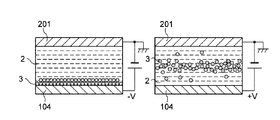
次に、階調表示の原理について説明する。図4は分割セルの構造を簡略化して示した断面図である。この例の電気泳動表示装置にあっては、まず、図4の左側に示すように電気泳動粒子3を画素電極104側に引き寄せる。正に帯電した電気泳動粒子3を用いるとすれば、共通電極201の電圧を基準として負極性の電圧を画素電極104に所定時間給電する。以下の説明では、このように一方の電極に電気泳動粒子3を引き寄せる動作をリセット動作と呼ぶことにする。
【0038】
次に、図4の右側に示すように正極性の電圧を画素電極104に印加する。すると、クローン力によって電気泳動粒子3は共通電極201側に移動する。一方、電圧の印加を停止すると、クーロン力が作用しなくなるので、電気泳動粒子3は分散媒2の粘性抵抗によって停止する。電気泳動粒子3の移動速度は、電界強度、すなわち印加電圧に応じて定まる。したがって、電気泳動粒子3の移動距離は、印加電圧と印加時間に応じて定まる。印加電圧を一定にすれば、印加時間を調整することによって、電気泳動粒子3の位置を厚さ方向に制御できる。
【0039】
共通電極201から入射した光は電気泳動粒子3によって反射され、この反射光が共通電極201を通過して観測者の目に至る。入射光と反射光は分散媒2によって吸収され、その程度は光路長に比例する。したがって、観測者が認識する階調は、電気泳動粒子3の位置によって定まることになる。上述したように、印加電圧を一定にしたとき電気泳動粒子3の厚さ方向の位置は、印加時間に応じて定まるから、表示すべき階調に応じた時間だけ一定電圧を印加すれば、所望の階調表示を得ることができる。
【0040】
ところで、分散系1は多数の電気泳動粒子3を含んでいる。ここで、電気的特性(例えば、電荷量)や機械的特性(例えば、粒子径、重量)等の粒子特性が、総ての粒子について揃っているとすれば、総ての粒子は同一の速度で移動する。つまり、総ての電気泳動粒子3は同じようにふるまうことになる。
【0041】
分割セル11cの厚さは数μm〜数10μmであり、最大移動距離は極めて短い。このため、階調数を多くしようとすると、微小な移動距離を制御する必要がある。すると、1階調分の印加時間が極めて小さくなり、階調制御が困難になる。
【0042】
そこで、本実施形態の電気泳動粒子3には、粒子特性にバラツキを持たせてある。粒子特性にバラツキを持たせると、ある一定電圧をある時間印加したとき電気泳動粒子3の位置は広がりを持つ。図5は、電圧の印加時間と階調濃度との関係の一例を示すグラフである。このグラフは、以下の条件下にシュミレーションをして得られたものである。第1の条件は、5Vの電圧を印加したとき、電気泳動粒子3が共通電極201に到達する時間の平均値が50msecであることである。第2の条件は、到達するのに要する印加電圧の標準偏差が2msecであることである。
【0043】
図5において、実線は印加時間に対する階調特性を示しており、点線は印加時間に対する確率密度を示している。ここで、確率密度とは、共通電極201に到達する電気泳動粒子3の個数を、平均値50msecで正規化したものである。この図に示すように、印加時間が45msec以下の場合には、電気泳動粒子3が殆ど共通電極201に到達しない。印加時間が50msecの場合には、半分の電気泳動粒子3が共通電極201に到達する。さらに印加時間が55msec以上の場合には殆どの電気泳動粒子3が共通電極201に到達する。したがって、表示すべき階調に応じて印加時間を45msecから55mescの間で制御すれば、所望の階調表示を行うことが可能となる。
【0044】
<1−3:駆動回路>
次に、各走査線101および各データ線102を駆動する駆動回路について説明する。まず、図3に示す走査線駆動回路130Aは、シフトレジスタを有する。走査線駆動回路130Aは、Yクロック信号YCKおよび反転YクロックYCKBに基づいて、Y転送開始パルスDYを順次シフトして、走査線信号Y1、Y2、…、Ymを生成する。Y転送開始パルスDYは垂直走査期間の開始から一定期間アクティブとなる。タイミングジェネレータ400Aは、Yクロック信号YCK、反転YクロックYCKB、およびY転送開始パルスDYを走査線駆動回路130Aに供給する。これにより、走査線信号Y1、Y2、…、Ymのアクティブ期間(Hレベル期間)は、図7に示すように順次シフトしていく。
【0045】
次に、データ線駆動回路140Aについて説明する。図6はデータ線駆動回路140Aのブロック図である。図7はデータ線駆動回路140Aのタイミングチャートである。図6に示すようにデータ線駆動回路140Aは、Xシフトレジスタ141、バスBUS、スイッチSW1〜SWn、第1ラッチ142、第2ラッチ143、およびPWM回路145を備えている。バスBUSには6ビットの画像データDが外部から供給される。
【0046】
まず、Xシフトレジスタ141は、XクロックXCKおよび反転XクロックXCKBにしたがって、X転送開始パルスDXを順次シフトする。これにより、図7に示すサンプリングパルスSR1、SR2、…、SRnが生成される。
次に、第1ラッチ142は複数のラッチ回路を含む。バスBUSは、スイッチSW1〜SWnを介して第1ラッチ群142の各ラッチ回路に接続されている。スイッチSW1〜SWnの各制御入力端子には、サンプリングパルスSR1、SR2、…、SRnが供給される。したがって、サンプリングパルスSR1、SR2、…、SRnに各々同期して、画像データDが第1ラッチ142に取りこまれる。なお、図6に示す各スイッチSW1〜SWnは、実際には各々6個のスイッチ回路の組から構成される。6ビットの画像データDに対応するためである。
【0047】
次に、第1ラッチ142は、スイッチSW1〜SWnから供給される画像データDをラッチする。これにより、点順次の画像データDa1〜Danが得られる(図7参照)。また、第2ラッチ143は、点順次の画像データDa1〜DanをラッチパルスLATによってラッチする。ここで、ラッチパルスLATは、図7に示すように1水平走査期間毎にアクティブとなる信号である。したがって、この第2ラッチ143は、点順次の画像データDa1〜Danの位相を水平走査期間毎に揃えて、線順次の画像データDb1〜Dbnを生成する。
【0048】
図8は、PWM回路145の構成を示すブロック図である。この図に示すようにPWM回路145は、n個の単位回路R1〜Rnとカウンタ144とを備えている。各単位回路R1〜Rnは、比較器1451、SRラッチ1452、および選択回路1453を備えている。
【0049】
カウンタ144は、水平走査期間の始まりからクロック信号CKをカウントして、そのカウント結果を示すカウントデータCNTを生成する。比較器1451は、線順次の画像データDb1〜DbnとカウントデータCNTとを比較して比較信号CSを生成する。比較信号CSは、線順次の画像データDb1〜DbnとカウントデータCNTとが一致する場合にHレベルとなる一方、不一致の場合にLレベルとなる。比較信号CSは、SRラッチ1452のリセット端子に供給される。SRラッチ1452のセット端子には、セット信号SETがタイミングジェネレータ400Cから供給される。セット信号SETは水平走査期間の始まりから所定期間Hレベルとなる。
【0050】
各単位回路R1〜RnのSRラッチ1452は、PWM信号(パルス幅変調信号)W1〜Wnを生成する。PWM信号W1〜Wnは、セット信号SETがHレベルになるとHレベルとなり、その後、比較信号CSがHレベルになるとLレベルになる。
【0051】
図9は、線順次の画像データの値とPWM信号の波形を示したタイミングチャートである。この図に示すように、各PWM信号のアクティブ(Hレベル)期間は、線順次の画像データの指示する階調値に応じた期間となる。もっとも、階調値が「111111」(100%)の場合であっても、1水平走査期間に占めるPWM信号のアクティブ期間の割合が2/3程度になるようにクロック信号CKの周波数が選ばれている。
【0052】
次に、各選択回路1453は、PWM信号W1〜Wnとリセットタイミング信号Crとに基づいて、共通電極電圧Vcom、印加電圧Va、およびリセット電圧Vrestの中から所定の電圧を選択して出力する。選択条件は以下の通りである。第1に、選択回路1453は、リセットタイミング信号Crがアクティブ(Hレベル)のときにリセット電圧Vrestを選択する。第2に、選択回路1453は、リセットタイミング信号Crが非アクティブ(Lレベル)かつPWM信号がアクティブ(Hレベル)のときに印加電圧Vaを選択する。第3に、選択回路1453は、リセットタイミング信号Crが非アクティブ(Lレベル)かつPWM信号が非アクティブ(Lレベル)のときに共通電極電圧Vcomを選択する。
【0053】
ここで、j番目の単位回路Rjの動作を図10に示すタイミングチャートを参照して、具体的に説明する。なお、この例では、ある水平走査期間において、リセットタイミング信号Crは非アクティブになっており、また、線順次の画像データDbjが指示する階調値が「32」であるものとする。
【0054】
この図に示すように、水平走査期間の開始時刻Tssから、カウントデータCNTが増加し始めるとともにセット信号SETがアクティブになる。PWM信号Wjはセット信号に同期してHレベルとなる。そして、時刻Teに至ると、カウントデータCNTの値が「32」になり、比較信号CSがアクティブとなる。すると、PWM信号WjがHレベルからLレベルに遷移する。この結果、時刻Tssから時刻Teまでの期間において、PWM信号WjはHレベルとなる。
【0055】
上述したように選択回路1453は、PWM信号WjがHレベルとなる期間において印加電圧Vaを選択する一方、そのLレベル期間あっては共通電極電圧Vcomを選択する。したがって、データ線信号Xjは、図10に示すように、時刻Tsから時刻Teまでの期間において印加電圧Vaとなる一方、時刻Teから当該水平走査期間が終了するまで共通電極電圧Vcomとなる。
【0056】
つまり、データ線信号Xjは、表示すべき階調に応じた期間だけ一定電圧となり、他の期間にあっては共通電極電圧Vcomとなる。このようにして、データ線駆動回路140Aは、データ線信号X1〜Xnを各々生成し、これらを各データ線102に供給する。
【0057】
<1−4:電気泳動表示装置の動作>
次に、電気泳動表示装置の動作について説明する。
【0058】
<1−4−1:全体動作>
図11は電気泳動表示装置の全体動作を示すタイミングチャートである。この図を参照しつつ、動作の概要を説明する。まず、時刻t0において、電気泳動表示装置の電源がオフ状態からオン状態に切り替わると、画像信号処理回路300A、タイミングジェネレータ400Aおよび電気泳動表示パネルAに電源が給電される。
【0059】
そして、所定期間が経過し回路動作が安定した時刻t1において、タイミングジェネレータ400Aは、リセットタイミング信号Crを1フィールド期間アクティブにする。このリセット期間Trにあっては、表示原理で説明したように、電気泳動粒子3が画素電極104側に引き寄せられる。この結果、電気泳動粒子3の空間的な状態が初期化される。
【0060】
データ線駆動回路140Aの各選択回路1453は、当該期間においてリセット電圧Vrestを選択し、これをデータ線信号X1〜Xnとして各データ線102に出力する。そして、走査線駆動回路130Aが各走査線101を順次選択することにより、総ての画素電極104にリセット電圧Vrestが書き込まれる。
【0061】
次に、時刻t2に至ると、書込期間Twが開始する。この書込期間Twにあっては、画像信号処理回路300Aは1フィールド期間にわたって画像データDを出力する。各画素電極104には表示すべき階調に応じた期間だけ印加電圧Vaが書き込まれ、1枚の表示画面が完成することになる。
【0062】
次に、時刻t3から時刻t4までの保持期間Thは、直前の書込期間Twで書き込まれた画像を保持する期間である。保持期間Thの長さは任意に設定できる。当該期間において、画像信号処理回路300Aは動作を停止する。また、画素電極104と共通電極201との間には、電界が発生しないようになっている。電気泳動粒子3はクーロン力によって泳動するから、電界がなければ空間的な状態に変化がない。したがって当該期間にあっては、静止画像が表示されることになる。
【0063】
次に、時刻t4から時刻t6までの期間は画像を書き換えるための書換期間Tcである。書換期間Tcでは、時刻t1から時刻t3までの期間と同様に、リセット動作と書込動作が行われる。これにより、表示画面の更新を行うことができる。
【0064】
<1−4−2:リセット動作>
次に、リセット動作について詳細に説明する。図12はリセット動作における電気泳動表示装置のタイミングチャートである。なお、以下の説明では、i行j列の画素をPijと、画素Pijの画素電極104の印加電圧をVijと表すことにする。上述したようにリセット期間Trにあっては、リセットタイミング信号Crが図12に示すようにアクティブ(Hレベル)となるので、データ線信号X1〜Xnの電圧はリセット電圧Vrestとなる。
【0065】
この例では、電気泳動粒子3に正電荷が帯電しているので、リセット電圧Vrestは共通電極電圧Vcomを中心として負極性の値を取る。ここで、走査線信号Y1がアクティブ(Hレベル)になると、第1行目のTFT103がオン状態となり、リセット電圧Vrestが各画素電極104に書き込まれる。以後、第2行目、第3行目、…、第m行目の各画素電極104にリセット電圧Vrestが書き込まれる。例えば、時刻txにおいて走査線信号Y1がアクティブから非アクティブに変化すると、第1行目の各TFT103がオフ状態になり、画素電極104とデータ線102とが切断される。しかしながら、TFT103がオフ状態になっても第1行目の画素電極104ではリセット電圧Vrestが維持される。各画素は、画素電極104、分散系1、および共通電極201等によって構成される画素容量を備えており、画素容量にリセット電圧Vrestに相当する電荷が蓄積されるからである。
【0066】
こうして画素電極104にリセット電圧Vrestが印加されると、分散系1中の電気泳動粒子3が画素電極104に引き寄せられ、その空間的な状態が初期化される。
【0067】
<1−4−3:書込動作>
次に、書込動作について詳細に説明する。図13は書込動作における電気泳動表示装置のタイミングチャートである。ここでは、i行(i番目の走査線)・j列(j番目のデータ線)の画素における書込動作を説明する。他の画素においても同様の書き込みがなされることは勿論である。なお、以下の説明では、画素Pijの輝度をIijと表すことにする。
【0068】
j番目のデータ線102に供給されるデータ線信号Xjは、図12に示すように、PWM信号Wjのアクティブ期間である電圧印加期間Tvにおいて印加電圧Vaとなる。一方、PWM信号Wjの非アクティブ期間である無バイアス期間Tbにおいて、PWM信号Wjは共通電極電圧Vcomとなる。なお、実線で示すデータ線信号Xjの波形は表示すべき階調が100%の場合であり、一点鎖線で示すデータ線信号Xjの波形は表示すべき階調が50%の場合である。
【0069】
また、i番目の走査線101に供給される走査線信号Yiはi番目の水平走査期間においてアクティブとなる。このため、画素PijのTFT103は当該水平走査期間においてオン状態となり、画素Pijの画素電極104には、時刻T1から時刻T3までのデータ線信号Xjが取り込まれることになる。すなわち、この例ではある走査線のある選択期間において、画素電極104に印加電圧Vaを書き込んでから、共通電極電圧Vcomを書き込むまでの動作が終了する。
【0070】
次に、画素Pijにおける電気泳動粒子3の挙動について考察する。この書込動作の前には上述したリセット動作が行われているから、時刻T1において、画素Pijの電気泳動粒子3は画素電極104側に総て位置している。このとき、画素電極104に印加電圧Vaが印加されると、画素電極104から共通電極201へ向けて電界が付与される。したがって、時刻T1から電気泳動粒子3は移動を開始する。
【0071】
この例の電気泳動粒子3は白色であり分散媒2は黒色であるから、電気泳動粒子3が共通電極201に近づくほど、画素Pijの輝度Iijは高くなる。したがって、図13に示すように輝度Iijは、時刻T1から次第に高くなる。
【0072】
ところで、画素Pijは、画素電極104と共通電極201との間に分散系1を挟持して構成されている。このため、画素Pijは、等価的に、電極面積、電極間の距離、および分散系1の誘電率に応じた容量値を有する画素容量を含む。したがって、TFT103をオフ状態にして画素電極104への給電を停止したとしても、画素容量には電荷が蓄積される。よって、両電極間には一定の電界が継続して発生することになる。電界が付与される限り電気泳動粒子3は共通電極201に向けて泳動を続けるので、電界の発生を停止する期間、換言すれば、画素容量に蓄積されている電荷を取り去る工程が必要となる。無バイアス期間Tbはこのために設けられたものである。
【0073】
無バイアス期間Tbにあっては、共通電極電圧Vcomが画素電極104に印加されるので、時刻T2において画素電極104と共通電極201との電圧が一致する。このため、時刻T2から電気泳動粒子3にクーロン力が作用しなくなる。ここで、分散媒2の粘性抵抗がある程度大きいとすれば、電気泳動粒子3は外力が作用しなくなくなる時刻T2において泳動を停止する。この結果、輝度Iijは図13に示すように時刻T2から一定の値を取ることになる。なお、分散媒2の粘性抵抗が小さい場合にはクーロン力が作用しなくなっても電気泳動粒子3が惰性で泳動した後に停止する。そのような場合には、画像信号処理回路300Aにおいて、惰性による泳動を見込んで補正した画像データDを生成すればよい。
【0074】
この書込動作にあっては、まず、画素Pijの画素電極104に印加電圧Vaを階調に応じた電圧印加期間Tvだけ印加する。すると、電気泳動粒子3が表示すべき階調に応じた距離だけ移動する。次に、画素電極104に共通電極電圧Vcomを書き込んで、電気泳動粒子3の泳動を停止させる。これらの2つの工程によって、の画素Pijの輝度Iijを表示すべき階調に応じたものとすることができる。
【0075】
なお、この例では、電気泳動粒子3の泳動を停止させるために共通電極電圧Vcomを書き込んだ。しかし、完全に共通電極電圧Vcomと一致する電圧を書き込む必要はなく、電気泳動粒子3の泳動を停止させることができる電圧であればよい。電気泳動粒子3は粘性抵抗に打ち勝たなければ泳動できないので、分散媒2の粘性抵抗などが大きい場合には、無バイアス期間Tbの電圧が共通電極電圧Vcomと多少相違してもよい。
【0076】
<1−4−4:保持動作>
次に、保持動作について説明する。図13において、時刻T3に至ると、走査線信号Yiはアクティブから非アクティブに遷移するので、画素PijのTFT103はオフ状態となる。上述したように無バイアス期間Tbにおいて画素電極104には共通電極電圧Vcomが印加されるから電界が発生しないことになる。
【0077】
したがって、新たな電圧を画素電極104に書き込まない限り、分散系1には電界が付与されない。この結果、分散系1中の電気泳動粒子3の空間的な状態は保持されることになる。つまり、表示画像の内容を保持することができる。
【0078】
保持期間Thにあっては、画素電極104に電圧を書き込む必要がないので、走査線信号Y1〜Ymを生成する必要もなければ、データ線信号X1〜Xnを生成する必要もない。このため、当該期間にあっては、以下に述べる各種の方法で消費電力を削減できる。
【0079】
第1の方法は、電気泳動表示装置自体の主電源をオフ状態にすることである。これにより、電気泳動表示パネルAや周辺回路たる画像信号処理回路300Aおよびタイミングジェネレータ400Aは動作を停止することになり、一切電力を消費しないことになる。
【0080】
第2の方法は、電気泳動表示パネルAへの給電を停止することである。これにより、電気泳動表示パネルAで消費される電力を削減することができる。
【0081】
第3の方法は、YクロックYCKおよび反転YクロックYCKBと、XクロックXCK、反転XクロックXCKB、およびクロック信号CKを、走査線駆動回路130Aおよびデータ線駆動回路140Aへ供給するのを停止することである。 上述したように走査線駆動回路130Aおよびデータ線駆動回路140Aは相補型のTFTで構成されているため、電流が流れるときだけ、換言すれば、論理レベルの反転があるときに限り電力を消費する。したがって、クロックの供給を停止することによって消費電力を削減することが可能となる。
【0082】
<1−4−5:書換動作>
次に、表示画面の内容を書き換える書換動作について説明する。書換動作にあっては、以下に述べる各種の態様がある。
まず、第1の態様では、上述したリセット動作を行って各行毎に順次初期化を行い、次に、上述した書込動作を行って各行毎に順次、パルス幅変調されたデータ線信号X1〜Xnを画素電極104に書き込む。これにより、画面全体を書き換えることが可能となる。
【0083】
次に、第2の態様では、書き換えが必要となるラインに限って、リセット動作と書込動作を行う。ここでは、一例として第j番目と第j+1番目のラインを書き換える場合について説明する。図14は第2の態様に係るリセット動作を説明するためのタイミングチャートである。
【0084】
まず、リセット期間Trにあっては、画像信号処理回路300Aが画像データDとして共通電極電圧Vcomを指示するデータを出力する。すなわち、画像データDの値は当該期間中「0」となっている。また、走査線駆動回路130Aは、図14に示すように走査線信号Y1、…、Yj、Yj+1、…、Ymを順次出力する。
【0085】
次に、リセットタイミング信号Crは、書き換えるべき走査線101を選択する期間にのみLレベルとなる。この例では、j番目とj+1番目のラインを書き換えるので、走査線信号Yj、Yj+1がアクティブとなる期間中にリセットタイミング信号CrはLレベル(非アクティブ)となる。上述したように選択回路1453(図8参照)はリセットタイミング信号CrがHレベル(アクティブ)のときに共通電極電圧Vcomを出力する一方、リセットタイミング信号CrがLレベルのときにPWM信号を出力する。ここで、画像データDの値は「0」であるから、PWM信号は常に非アクティブ(Lレベル)となる。
【0086】
したがって、j番目とj+1番目の走査線101を選択する期間にあっては、総てのデータ線102にリセット電圧Vrestが供給される。そして、他の走査線101の選択期間にあっては、総てのデータ線102に共通電極電圧Vcomが供給される。
【0087】
この結果、図14に示すように第1行〜第j−1行目と第j+2〜第m行の画素電極104には共通電極電圧Vcomが供給される。また、第j行および第j+1行の画素電極104には、リセット電圧Vrestが供給される。したがって、第j行および第j+1行の画素にあっては、電気泳動粒子3の空間的な状態が初期化されることになる。一方、共通電極電圧Vcomが画素電極104に書き込まれても電界は発生しないので、第1行〜第j−1行目と第j+2〜第m行の画素では電気泳動粒子3の空間的な状態が変化しない。
【0088】
次に、書込動作にあっては、画像信号処理回路300Aは、書き換えるべきラインについてのみ有効な画像データDを出力し、他のラインについては画像データDの値を「0」にする。これにより、第j行と第j+1行に限って書き換えを行うことができる。
【0089】
次に、第3の態様では、書き換えるべき複数のラインを同時にリセットして、この後,通常の書込動作によって書き換えを行う。第2の態様では、第j行の次に第j+1行をリセットするといったように、行毎に順次リセット動作を行った。書き換えるべき複数の走査線101を同時に選択できる走査線駆動回路を用いれば、同時にリセットを行うことが可能である。例えば、図15に示すように、走査線信号Yj、Yj+1のみを同時にアクティブにして、データ線102にリセット電圧Vrestを供給すれば、図16に示すように書き換えるべきj番目とj+1番目のラインを同時にリセットすることができることは勿論である。また、書込動作にあっては、画像信号処理回路300Aが書き換えるべきラインについてのみ有効な画像データDを出力し、他のラインについてはそのデータ値を「0」とする。そして、通常の書込動作と同様に書き込みを行う。これにより、第j行と第j+1行に限って書き換えを行うことができる。
【0090】
次に、第4の態様では総ての画素を同時にリセットして、この後、通常の書込動作を行って書き換えを実行する。図17は、第4の態様に係る電気泳動パネルBのブロック図である。この電気泳動パネルBは、各列毎にTFT105が設けられている点、および走査線駆動回路130Bが総ての走査線信号Y1〜Ymを同時にアクティブとできるようになっている点を除いて、図3に示す電気泳動パネルAと同様に構成されている。
【0091】
図17において、各TFT105のソース電極にはリセット電圧Vrestが供給される。各TFT105のゲート電極にはリセットタイミング信号Crが供給される。さらに、各TFT105のドレイン電極は各データ線102に接続されている。リセットタイミング信号Crがアクティブになると、総てのTFT105が同時にオン状態となって、リセット電圧Vrestが各データ線102に供給される。一方、走査線駆動回路130Bは、リセットタイミング信号Crがアクティブになると、総ての走査線信号Y1〜Ymを同時にアクティブにする。したがって、リセットタイミング信号Crのアクティブ期間に、総ての画素電極104にリセット電圧Vrestが書き込まれる。これにより、総ての画素が同時にリセットされる。
【0092】
なお、この場合にTFT105の各ソース電極を接地しておき、共通電極電圧Vcomとして接地電位を基準として初期化するのに十分な正極性の電圧を給電するようにしてもよい。すなわち、画素電極104と共通電極201とのうちいずれか一方の電位を基準として、他方の電極に初期化するのに十分な電圧を印加すればよい。なお、共通電極201を分割して複数の分割電極(例えば、上半分と下半分)を設けておき、書き換えるべき画像領域が属する分割電極に初期化するための電圧を給電するようにしてもよい。
【0093】
<2:第2実施形態>
<2−1:第2実施形態の概要>
上述した第1実施形態では、画面を書き換える際には、図18の右側に示すリセット動作を行った後、図18の中央に示す書き込み動作を行い、表示画面を更新していた。この場合、電気泳動粒子3の空間的な状態は一旦初期化される。例えば、分散媒2が黒色に着色されており、電気泳動粒子3が白色であるとすれば、表示を更新する際に、画面全体が暗転(黒)することになる。人の視覚は短時間の変化を検知することができないので、リセット動作に要する期間が短ければ、次々と画面を更新することによって、動画を表示することも可能である。
【0094】
しかしながら、分散系1の物理的な性質によっては、リセット動作に長い時間を必要とし、電気泳動粒子3の初期化に伴う輝度変化が人に検知されることもある。
【0095】
そこで、第2実施形態の電気泳動表示装置は、第1に、次に表示すべき階調に対応する電気泳動粒子の平均位置と、現在表示中の階調に対応する電気泳動粒子の平均位置との差分を算出し、第2に差分に相当する時間、電極間に一定電圧を印加するようにしている。例えば、現在の階調が50%であり、これを75%の階調に変化させる場合を想定する。図18の中央に示すように電気泳動粒子3の平均的な位置が分散系1の厚さ方向の約1/2にあると、表示階調は50%になる。この階調を75%に変化させるためには、図18右側に示すように電気泳動粒子3の平均的な位置を厚さ方向に約3/4まで移動させる必要がある。そこで、次に表示すべき階調と現在の階調との差分に応じた期間だけ画素電極104に一定電圧を印加する。これにより、電気泳動粒子3は表示階調に応じた位置まで移動するから、表示画面の更新が可能となる。リセット動作を行うことなく画面の更新が可能となる点は、動画を表示する場合に重要である。
【0096】
<2−2:電気泳動表示装置の構成>
第2実施形態の電気泳動表示装置は、画像信号処理回路300Aの替わりに画像信号処理回路301Aを用いる点、データ線駆動回路140AにおいてPWM回路145の替わりにPWM回路145Aを用いる点を除いて、図3に示す第1実施形態の電気泳動表示装置と同様に構成されている。
<2−2−1:画像信号処理回路>
図19は画像信号処理回路301Aの構成を示すブロック図である。この図に示すように、画像信号処理回路300Aは、A/D変換器310、補正部320、および演算部330を備えている。外部から供給される画像信号VIDはA/D変換器310を介して入力画像データDinに変換される。補正部320はROM等を有している。補正部320は、入力画像データDinにガンマ補正等の補正処理を施して、画像データDvを生成する。
【0097】
次に、演算部330は、メモリ331と減算器332と備えている。画像データDvは減算器332の一方の入力端子とメモリ331とに供給される。メモリ331は、第1フィールドメモリ331Aと第2フィールドメモリ331Bとを備えている。第1フィールドメモリ331Aは、奇数フィールドで書込動作を行う一方、偶数フィールドで読出動作を行う。第2フィールドメモリ331Bは、奇数フィールドで読出動作を行う一方、偶数フィールドで書込動作を行う。このメモリ331によって画像データDvは1フィールド遅延される。遅延された画像データDvは、遅延画像データDv’として減算器332の他方の入力端子に供給される。減算器332は、画像データDvから遅延画像データDv’を減算して差分画像データDdを生成し、これを出力する。この差分画像データDdのMSBは符号ビットとなっており、そのデジットが「0」のとき正を、「1」のとき負を示すようになっている。
【0098】
なお、最初のフィールドにあっては、遅延画像データDv’が存在しないので、減算器332の他方の入力端子には、データ値が‘0’となるダミーデータが供給されるようになっている。したがって、最初のフィールドでは、画像信号処理回路301Aは、画像データDvを差分画像データDdとして出力する。
【0099】
ここで、遅延画像データDv’を現在の表示階調とすれば、画像データDvは次に表示すべき階調に相当する。したがって、差分画像データDdは現在の階調と次に表示すべき階調の差分に応じたデータとなる。差分画像データDdは、画像データDの替わりにデータ線駆動回路140Aに供給される。
【0100】
<2−2−2:PWM回路>
図20は、PWM回路145Aの構成を示すブロック図である。PWM回路145Aが図8に示すPWM回路145と相違するのは、データDb1〜Dbnを最上位ビットと他のビットとに分けて処理する点である。PWM回路145Aにおいては、データDb1〜Dbnの最上位ビットが選択信号Msとして選択回路1453Aに供給される。また、データDb1〜Dbnから最上位ビットを除いたものは、比較器1451に供給される。比較器1451は下位ビットとカウントデータCNTを比較して比較信号CSを生成する。
【0101】
また、選択回路1453Aは、PWM信号W1〜Wn、リセットタイミング信号Cr、および選択信号Msに基づいて、共通電極電圧Vcom、印加電圧+Va、−Vaおよびリセット電圧Vrestの中から所定の電圧を選択して出力する。
【0102】
選択条件は以下の通りである。第1に、選択回路1453Aは、リセットタイミング信号Crがアクティブ(Hレベル)のときにリセット電圧Vrestを選択する。第2に、選択回路1453Aは、リセットタイミング信号Crが非アクティブ(Lレベル)かつPWM信号がアクティブ(Hレベル)かつ選択信号MsがHレベルのとき、印加電圧+Vaを選択する。第3に、選択回路1453Aは、リセットタイミング信号Crが非アクティブ(Lレベル)かつPWM信号がアクティブ(Hレベル)かつ選択信号MsがLレベルのとき、印加電圧−Vaを選択する。第4に、選択回路1453Aは、リセットタイミング信号Crが非アクティブ(Lレベル)かつPWM信号が非アクティブ(Lレベル)のときに共通電極電圧Vcomを選択する。
【0103】
第1実施形態と異なり、選択回路1453Aにおいて、選択信号Msに基づいて印加電圧+Vaと−Vaを選択したのは、以下の理由による。第1実施形態では、画像を更新する場合、画素電極104にリセット電圧Vrestを印加して、電気泳動粒子3を画素電極104に引き寄せた。このため、書込期間Twにおいては、電気泳動粒子3を画素電極104側からから共通電極201側へ移動させればよかった。つまり、書込期間Twにおける電気泳動粒子3の移動方向は一方向に限られていた。これに対して、第2実施形態では、差分画像データDdに基づいて電気泳動粒子3の位置を制御するため、電気泳動粒子3を両方向に移動させる必要がある。そこで、選択信号Msに基づいて、共通電極電圧Vcomを基準として正極性の電圧+Vaと負極性の電圧−Vaとを選択できるようにしたのである。
【0104】
<2−3:電気泳動表示装置の動作>
次に、電気泳動表示装置の動作について説明する。図21は電気泳動表示装置の全体動作を示すタイミングチャートである。この図を参照しつつ、動作の概要を説明する。
【0105】
まず、時刻t0において、電気泳動表示装置の電源がオフ状態からオン状態に切り替わると、画像信号処理回路301A、タイミングジェネレータ400Aおよび電気泳動表示パネルAに電源が給電される。そして、所定期間が経過し回路動作が安定した時刻t1において、タイミングジェネレータ400Aは、リセットタイミング信号Crを1フィールド期間アクティブにする。このリセット期間Trにあっては、データ線駆動回路140Aはリセット電圧Vrestを各データ線102に出力する。また、走査線駆動回路130が各走査線101を順次選択する。これにより、総ての画素電極104にリセット電圧Vrestが書き込まれると、電気泳動粒子3が画素電極104側に移動する。つまり、電気泳動粒子3の空間的な状態が初期化される。
【0106】
次に、時刻t2に至ると、書込期間Twが開始する。この書込期間Twにあっては、画像信号処理回路300Aは差分画像データDdを出力する。各画素電極104には表示中の階調と次に表示すべき階調との差に応じた時間だけ印加電圧+Vaまたは−Vaが書き込まれる。ただし、最初のフィールド(時刻t2から時刻t3まで)にあっては、画像データDvが差分画像データDdとしてデータ線駆動回路140Aに供給されるから、表示すべき階調に応じた期間だけ印加電圧+Vaが各画素電極104に書き込まれることになる。もっとも、リセット動作によって、表示階調は0%(あるいは100%)になっているから、基本的な機能に着目すれば、最初のフィールドにあっても、表示中の階調と次に表示すべき階調との差分に応じた期間だけ印加電圧+Vaを書き込んでいるといえる。
【0107】
<2−3−1:書込動作>
次に、書込動作について詳細に説明する。図22は書込動作における電気泳動表示装置のタイミングチャートである。ここでは、i行(i番目の走査線)・j列(j番目のデータ線)の画素における書込動作を説明する。他の画素においても同様の書き込みがなされることは勿論である。この例では、直前のフィールドにおいて画素Pijは100%の階調レベルを表示したものとする。くわえて、現在のフィールドで表示すべき階調が50%の場合を実線で、0%の場合を一点鎖線で示す。
【0108】
j番目のデータ線102に供給されるデータ線信号Xjの電圧は、図22に示す差分電圧印加期間Tdvにおいて印加電圧+Vaまたは−Vaとなる。現在のフィールドで表示すべき階調が50%であれば、直前のフィールドの階調より50%減少している。このため、図22に示すように差分電圧印加期間Tdvでは印加電圧−Vaが選択される。一方、無バイアス期間TdbはPWM信号Wjが非アクティブとなる期間である。
【0109】
また、i番目の走査線101に供給される走査線信号Yiはi番目の水平走査期間においてアクティブとなる。画素Pijを構成するTFT103は当該水平走査期間においてオン状態となる。画素Pijの画素電極104には、時刻T1から時刻T3までのデータ線信号Xjが取り込まれる。すなわち、この例ではある走査線のある選択期間において、画素電極104に印加電圧−Vaを書き込んでから、共通電極電圧Vcomを書き込むまでの動作が終了する。
なお、画像保持動作は第1実施形態を同様のため、説明を省略する。
【0110】
<3:第3実施形態>
次に、第3実施形態に係る電気泳動表示装置について説明する。第1実施形態の電気泳動表示装置にあっては、第1に、画素電極104に表示階調に応じた期間だけ印加電圧Vaを印加して、階調に応じた距離だけ電気泳動粒子3を移動させ、第2に、画素電極104に共通電極電圧Vcomを印加して電気泳動粒子3にクローン力を作用させないようにした。また、分散媒2の粘性抵抗が小さい場合には、共通電極電圧Vcomを印加した後も電気泳動粒子3が惰性で泳動するため、画像信号処理回路300Aにおいて、惰性による泳動を見込んで画像データDを生成していた。
【0111】
しかしながら、分散媒2の粘性抵抗の値によっては、電気泳動粒子3の運度エネルギーを減衰させるのに長時間を要する場合もある。上述した例では電気泳動粒子3が画素電極104から共通電極201に向けて泳動するから、粘性抵抗が極端に小さいと表示画面が次第に明るくなり、やがてある明るさに落ち着くことになる。
【0112】
第3実施形態は、このような表示画面の明るさの変動を防止できる電気泳動表示装置を提供するものである。第3実施形態の電気泳動表示装置は、画像信号処理回路300Aの替わりに画像信号処理回路300Bを用いる点、データ線駆動回路140Aの替わりにデータ線駆動回路140Bを用いる点を除いて、図3に示す第1実施形態の電気泳動表示装置と同様に構成されている。
【0113】
<3−1:画像信号処理回路>
まず、画像信号処理回路300Bについて説明する。図23は画像信号処理回路300Bのブロック図であり、図24はその出力データのタイミングチャートである。
【0114】
図23に示すように画像信号処理回路300Bは、A/D変換器310、補正部320、制動データ生成部330、および選択部340を備えている。A/D変換器310は画像信号VIDをアナログ信号からデジタル信号に変換して入力画像データDinを出力する。補正部320は、ROM等を有しており、入力画像データDinにガンマ補正等の補正処理を施して画像データDを生成する。
【0115】
制動データ生成部330は、その内部にテーブルを有している。このテーブルは、制動データDsのデータ値を画像データDの取り得るデータ値と対応付けて記憶する。制動データ生成部330は、画像データDをアドレスとして当該テーブルにアクセスして制動データDsを得る。なお、テーブルは、RAMやROM等の記憶回路を含む。ここで、制動データDsは、電気泳動粒子3の運動を減衰させるために用いられる。制動データDsは、制動電圧印加期間Tsに対応する。
【0116】
電気泳動粒子3には、印加電圧Va応じた電界によってクローン力が与えられる。電圧印加期間Tvにおいて、電気泳動粒子3はクローン力によって加速され泳動する。この後、分散系1に電界を付与することを停止しても、電気泳動粒子3は惰性による運動を続ける。その運動を減衰させるには、第1に逆向きの電界を印加する必要がある。第2に逆向きの電界を印加すべき期間は、電気泳動粒子3の運動エネルギー、換言すれば表示すべき階調に応じて定まる。そこで、本実施形態にあっては、分散媒2の粘性抵抗等を考慮した制動データDsを予め生成し、これを画像データDの値に対応付けてテーブルに予め記憶しておき、画像データDに基づいて制動データDsをテーブルから読み出す。
【0117】
次に、選択部340は、図24に示すように書込期間にあっては、画像データDと制動データDsを多重した多重データDmを出力する。この例において、画像データDは6ビット、制動データDsは6ビットである。多重データDmは12ビットのデータである。また、多重データDmは、MSBから6ビットが画像データD、LSBから6ビットが制動データDsとなる。
【0118】
<3−2:データ線駆動回路>
次に、データ線駆動回路140Bについて説明する。データ線駆動回路140BはPWM回路145Bの構成を除いて第1実施形態のデータ線駆動回路140Aと同様に構成されている。
【0119】
図25は、第3実施形態に用いるPWM回路145Bのブロック図であり、図26はそのタイミングチャートである。図25に示すように、このPWM回路145Bは、各単位回路R1〜Rnを備える。各単位回路R1〜Rnは、比較器1454とSRラッチ1455が追加された点、および選択回路1453の替わりに選択回路1456を用いる点で、図8に示す第1実施形態のPWM回路145と相違する。
【0120】
各単位回路R1〜Rnを構成する比較器1451には、多重データDmの上位ビットから構成される画像データDが供給される一方、比較器1454にはその下位ビットから構成される制動データDsが供給される。比較器1454は、比較信号CS’を生成する。比較信号CS’はカウントデータCNTと制動データDsとが一致したときにアクティブ(Hレベル)となる
【0121】
次に、各SRラッチ1455は、立ち下りエッジで出力レベルをセットし(Hレベル)、立ち上がりエッジでリセットする(Lレベル)。また、セット端子には各SRラッチ1452の出力信号たるPWM信号W1〜Wnが供給され、リセット端子には比較信号CS’が供給される。各SRラッチ1455の出力信号は、制動信号W1’〜Wn’として選択回路1456に供給される。
【0122】
次に、各選択回路1456は、リセットタイミング信号Cr、PWM信号W1〜Wnおよび制動信号W1’〜Wn’に基づいて、リセット電圧Vrest、印加電圧Va、制動電圧Vsおよび共通電極電圧Vcomの中から所定の電圧を選択して出力する。その選択条件は以下の通りである。
【0123】
第1に、選択回路1456は、リセットタイミング信号Crがアクティブ(Hレベル)のときにリセット電圧Vrestを選択する。第2に、選択回路1456は、リセットタイミング信号Crが非アクティブ(Lレベル)かつPWM信号がアクティブ(Hレベル)のときに印加電圧Vaを選択する。第3に、選択回路1456は、リセットタイミング信号Crが非アクティブ(Lレベル)かつ制動信号がアクティブ(Hレベル)のときに制動電圧Vsを選択する。第4に、選択回路1456は、リセットタイミング信号Cr、PWM信号および制動信号が非アクティブ(Lレベル)のときに共通電極電圧Vcomを選択する。
【0124】
ここで、j番目の単位回路Rjの動作を図26に示すタイミングチャートを参照して、具体的に説明する。なお、この例では、ある水平走査期間において、リセットタイミング信号Crは非アクティブになっており、また、線順次の画像データDbjは画像データDと制動データDsとを含む。この例の画像データDが指示する階調値は「32」である。また、この例の制動データDsが指示する値は「48」である。この図に示すように、PWM信号Wjは、水平走査期間の開始からカウントデータCNTの値が「32」になるまでの期間、Hレベルとなる(時刻t20から時刻t21までの期間)。
【0125】
SRラッチ1455はPWM信号Wjの立ち下りエッジでトリガされるので、時刻t21において制動信号Wj’はLレベルからHレベルへ遷移する。そして、時刻t22に至ると、カウントデータCNTの値が「48」になり、カウントデータCNTの値は制動データDsの値と一致する。このとき、比較信号CS’がLレベルからHレベルへ遷移し、この立ち上がりエッジに同期して制動信号Wj’がHレベルからLレベルへ遷移する。
【0126】
上述したように選択回路1455は、PWM信号WjがHレベルとなる期間において印加電圧Vaを選択し、制動信号Wj’がHレベルとなる期間において制動電圧Vsを選択し、これらの信号がLレベル期間あっては共通電極電圧Vcomを選択出力する。このため、データ線信号Xjの電圧は、図26に示すように、時刻t20から時刻t21までの期間において印加電圧Vaとなり、時刻t21から時刻t22までの期間において制動電圧Vsとなり、さらに、時刻t22から当該水平走査期間が終了するまで共通電極電圧Vcomとなる。このようにして生成されたデータ線信号X1〜Xnは、各データ線102に供給される。そして、データ線信号X1〜Xnは、走査線信号Y1〜Ymに同期して画素電極104に印加される。
【0127】
<3−3:電気泳動表示装置の動作>
次に、第3実施形態に係る電気泳動表示装置の動作について説明する。この電気泳動表示装置は、リセット動作→書込動作→保持動作→書換動作(リセット動作および書込動作)といった順に動作する点では、図11を参照して説明した第1実施形態の電気泳動表示装置と同様である。ただし、第3実施形態に係る電気泳動表示装置の動作は、書込動作(書換動作中のものを含む)中に、制動電圧Vsを所定期間だけ画素電極104に印加する工程が加えられている点で、第1実施形態に係る電気泳動表示装置の動作と相違する。以下、相違点である書込動作の詳細について説明する。
【0128】
図26は書込動作における電気泳動表示装置のタイミングチャートである。ここでは、i行j列の画素Pijにおける書込動作を説明する。他の画素においても同様の書込動作がなされる。
データ線信号Xjはj番目のデータ線102に供給される。データ線信号Xjの電圧は、図26に示すように、電圧印加期間Tvにおいて印加電圧Vaとなる。電圧印加期間Tvは時刻T1から時刻T2までの期間である。データ線信号Xjの電圧は、制動電圧印加期間Tsにおいて制動電圧Vsとなる。制動電圧印加期間Tsは時刻T2から時刻T3までの期間である。データ線信号Xjの電圧は、無バイアス期間Tbにおいて共通電極電圧Vcomとなる。無バイアス期間Tbは時刻T3から時刻T4までの期間である。
【0129】
また、走査線信号Yiはi番目の走査線101に供給される。走査線信号Yiはi番目の水平走査期間においてアクティブとなる。このため、画素PijのTFT103は当該水平走査期間においてオン状態となり、画素Pijの画素電極104には、時刻T1から時刻T4まで期間において、データ線信号Xjが印加される。すなわち、この例ではある走査線のある選択期間において、第1に画素電極104に印加電圧Vaを書き込み、第2に画素電極104に制動電圧Vsを書き込み、第3に画素電極104に共通電極電圧Vcomを書き込む。
【0130】
次に、画素Pijにおける電気泳動粒子3の挙動について考察する。この書込動作の前にはリセット動作が行われているから、時刻T1において、画素Pijの電気泳動粒子3は画素電極104側に総て位置している。このとき、画素電極104に印加電圧Vaが印加されると、画素電極104から共通電極201へ向けて電界が付与される。したがって、時刻T1から電気泳動粒子3は移動を開始し、輝度Iijは次第に高くなる。
【0131】
そして、時刻T2に至ると、画素電極104に制動電圧Vsが印加される。制動電圧Vsの印加期間は、直前の印加電圧Vaの印加期間に応じて設定されている。また、制動電圧Vsの極性は共通電極電圧Vcomを基準として負極性のものである。これは、電圧印加期間Tvにおいて、電気泳動粒子3には画素電極104から共通電極201へ向けてのクローン力が作用していたので、これを打ち消す方向に電界を付与する必要があるからである。
【0132】
この制動電圧Vsは、いわばブレーキとして電気泳動粒子3に作用する。制動電圧Vsは、電気泳動粒子3の運動方向とは逆方向のクローン力を電気泳動粒子3に付与する。これにより、制動電圧印加期間Tsの終了時刻T3までに電気泳動粒子3は泳動を停止する。
【0133】
そして、時刻T3に至ると、画素電極104には共通電極電圧Vcomが印加される。すると、画素電極104と共通電極201との電圧が一致するから、画素容量に蓄積されていた電荷が放電される。これにより、TFT103をオフ状態にしても画素Pijには電界が全く発生しないことになるので、電気泳動粒子3の空間的な状態を保持することができる。
【0134】
このように本実施形態の書込動作にあっては、まず、画素Pijの画素電極104に印加電圧Vaを表示すべき階調に応じた期間だけ書き込む。すると、電気泳動粒子3が移動する。さらに、画素Pijの画素電極104に制動電圧Vsを所定期間書き込む。すると、電気泳動粒子3の運動が減衰して電気泳動粒子3が停止する。したがって、分散媒2の粘性抵抗が小さい場合であっても、電気泳動粒子3の惰性による泳動距離を短くすることができる。この結果、輝度の変化がない安定した画像を短時間で表示させることが可能となる。
【0135】
<4:第4実施形態形態>
第4実施形態は、第2実施形態で説明した差分駆動に関する技術と第3実施形態で説明した電気泳動粒子3の制動に関する技術とを組み合わせたものである。第3実施形態の電気泳動表示装置においては、表示すべき階調に応じた期間だけ画素電極に一定電圧を印加したが、第4実施形態の電気泳動表示装置では次に表示すべき階調と現在表示中の階調の差分に対応した期間にわたって画素電極に一定電圧を印加する。
【0136】
第4実施形態の電気泳動表示装置は、画像信号処理回路301Aの替わりに画像信号処理回路301Bを用いる点、PWM回路145Aの替わりにPWM回路145Bを用いる点を除いて、第2実施形態の電気泳動表示装置と同様に構成されている。以下に相違点を中心に説明する。
【0137】
<4−1:画像信号処理回路>
まず、画像信号処理回路301Bについて説明する。図28は画像信号処理回路301Bのブロック図である。図28に示す画像信号処理回路301Bは、図19に示す第2実施形態の画像信号処理回路301Aと比較して、演算部330の後段に制動データ生成部350と選択部340とを備える点で相違する。
【0138】
制動データ生成部350は、テーブルを備える。テーブルは、RAMやROM等の記憶回路によって構成されている。テーブルは、制動データDdsのデータ値を差分画像データDdの取り得るデータ値と対応付けて記憶している。
【0139】
ここで、制動データDdsは、電気泳動粒子3の運動を減衰させるために用いられる。制動データDdsの値は後述する制動電圧印加期間Tdsに対応する。上述したように、電気泳動粒子3はクローン力によって加速され泳動する。この後、分散系1に電界を付与することを停止しても、電気泳動粒子3は惰性による運動を続ける。電気泳動粒子3を停止させるには、逆向きの電界を印加する必要がある。また、その電界強度は、電気泳動粒子3の運動エネルギー、換言すれば差分階調値に応じて定める必要がある。そこで、本実施形態にあっては、分散媒2の粘性抵抗等を考慮した制動データDdsを予め生成し、これを差分画像データDdの値に対応付けてテーブルに予め記憶しておき、差分画像データDdに基づいてテーブルから制動データDdsを読み出す。
【0140】
次に、選択部340は、差分画像データDdと制動データDdsとを選択することによって、これらを多重した多重データDdmを生成する。この例において、多重データDmは12ビットのデータであり、多重データDmは、MSBから6ビットが差分画像データDd、LSBから6ビットが制動データDdsとなる。
なお、選択部340の選択動作は、図24において画像データDを差分画像データDdに置き換えるとともに、制動データDsを制動データDdsに置き換えたものと同じである。
【0141】
<4−2:PWM回路>
図29は、PWM回路145Cの構成を示すブロック図である。図30は、多重データDdmとこれを分割して得られるデータの関係を示す図である。
図29に示すように、PWM回路145Cは、各単位回路R1〜Rnを備えている。各単位回路R1〜Rnには、多重データDdmが点順次の形式でデータDb1〜Dbnとして供給される。多重データDdmは、図30に示すように差分画像データDdと制動データDdsとからなる。差分画像データDdのうち、最上位ビットは選択信号Msであり、最上位ビットを除く下位5ビットが差分画像データDd’である。つまり、選択信号Msと差分画像データDd’とは、差分画像データDdの符号ビット(MSB)と絶対値を示す他のビットとを分離したものである。また、制動データDdsのうち最上位ビットは選択信号Ms’であり、最上位ビットを除く下位5ビットが制動データDds’である。つまり、選択信号Ms’と差分画像データDd’とは、差分画像データDdの符号ビット(MSB)と大きさを示す他のビットとを分離したものである。
【0142】
各単位回路R1〜Rnは、比較器1451、比較器1454および選択回路1456を備える。比較器1451は、5ビットのカウントデータCNTと差分画像データDd’とを比較して、比較信号CSを生成する。比較信号CS’はカウントデータCNTと差分画像データDd’が一致したときにアクティブ(Hレベル)となる。比較器1454は、カウントデータCNTと制動データDds’とを比較して、比較信号CS’を生成する。比較信号CS’はカウントデータCNTと制動データDds’が一致したときにアクティブ(Hレベル)となる。
【0143】
次に、各選択回路1456は、リセットタイミング信号Cr、PWM信号W1〜Wn、制動信号W1’〜Wn’、選択信号Ms,Ms’に基づいて、リセット電圧Vrest、印加電圧+Va、−Va、停止電圧+Vs、−Vsおよび共通電極電圧Vcomの中から所定の電圧を選択して出力する。
【0144】
選択条件は、以下の通りである。第1に、選択回路1456は、リセットタイミング信号Crがアクティブ(Hレベル)のときにリセット電圧Vrestを選択する。第2に、選択回路1456は、リセットタイミング信号Crが非アクティブ(Lレベル)かつPWM信号がアクティブ(Hレベル)のときに印加電圧+Vaまたは−Vaを選択する。第3に、選択回路1456は、リセットタイミング信号Crが非アクティブ(Lレベル)かつ停止信号がアクティブ(Hレベル)のときに制動電圧+Vsまたは−Vsを選択する。第4に、選択回路1456は、リセットタイミング信号Cr、PWM信号および停止信号が非アクティブ(Lレベル)のときに共通電極電圧Vcomを選択する。
【0145】
さらに、選択回路1456は、印加電圧+Vaまたは−Vaを選択するときには、選択信号MsがHレベルのとき印加電圧−Vaを選択し、それがLレベルのとき印加電圧+Vaを選択する。くわえて、選択回路1456は、制動電圧+Vsまたは−Vsを選択するときには、選択信号Ms’がHレベルのとき、制動電圧−Vsを選択し、それがLレベルのとき制動電圧+Vsを選択する。
【0146】
ここで、j番目の単位回路Rjの動作を図31に示すタイミングチャートを参照して、具体的に説明する。なお、この例では、ある水平走査期間において、リセットタイミング信号Crは非アクティブである。また、差分画像データDd’の指示する階調値が「16」、制動データDs’の指示する値が「24」である。くわえて、選択信号Msは「0」、選択信号Ms’は「1」である。
【0147】
PWM信号WjがHレベルとなる期間は、水平走査期間の開始からカウントデータCNTの値が「16」になるまでの期間である(時刻t20から時刻t21までの期間)。SRラッチ1455はPWM信号Wjの立ち下りエッジでトリガされるので、時刻t21において制動信号Wj’はLレベルからHレベルへ遷移する。そして、時刻t22に至ると、カウントデータCNTの値が「24」になり、制動データDs’の値と一致する。このとき、比較信号CS’がLレベルからHレベルへ遷移し、この立ち上がりエッジに同期して制動信号Wj’がHレベルからLレベルへ遷移する。
【0148】
上述したように選択回路1456は、PWM信号WjがHレベルとなる期間において印加電圧+Vaまたは−Vaを選択し、停止信号Wj’がHレベルとなる期間において停止電圧+Vsまたは−Vsを選択する。また、選択信号Ms、Ms’は、各々「0」、「1」であることから、選択回路1456は、印加電圧+Va、制動電圧−Vsが選択されることになる。さらに、PWM信号Wjおよび制動信号Wj’がLレベル期間あっては共通電極電圧Vcomが選択される。このため、データ線信号Xjの電圧は、時刻t20から時刻t21までの期間において印加電圧+Vaとなる。データ線信号Xjの電圧は、時刻t21から時刻t22までの期間において制動電圧−Vsとなる。さらに、データ線信号Xjの電圧は、時刻t22から当該水平走査期間が終了するまで期間、共通電極電圧Vcomとなる。
【0149】
<4−3:電気泳動表示装置の動作>
この電気泳動表示装置は、リセット動作→書込動作→保持動作といった順に動作する点では、図21を参照して説明した第2実施形態の電気泳動表示装置と同様である。ただし、書込動作中に、制動電圧を画素電極104に印加する工程が加えられている点で相違する。以下、相違点である書込動作の詳細について説明する。
【0150】
図32は書込動作における電気泳動表示装置のタイミングチャートである。ここでは、i行j列の画素Pijにおける書込動作を説明する。他の画素においても同様の書き込みがなされる。また、この例では、直前のフィールドにおいて画素Pijは100%の階調レベルを表示したものとする。くわえて、現在のフィールドで表示すべき階調が0%の場合を実線で、50%の場合を一点鎖線で示す。
【0151】
データ線信号Xjの電圧は、差分電圧印加期間Tdvにおいて印加電圧+Vaまたは−Vaとなる。現在のフィールドで表示すべき階調が50%であれば、直前のフィールドの階調より50%減少している。このため、図28に示すように差分電圧印加期間Tdvでは印加電圧−Vaが選択される。また、制動電圧印加期間Tdsにおいて、データ線信号Xjの電圧は制動電圧+Vsとなる。さらに時刻T3から時刻T4までの無バイアス期間Tdbにおいて、データ線信号Xjの電圧は共通電極電圧Vcomとなる。
【0152】
また、走査線信号Yiはi番目の水平走査期間においてアクティブとなる。このため、画素PijのTFT103は当該水平走査期間においてオン状態となる。画素Pijの画素電極104には、時刻T1から時刻T4までのデータ線信号Xjの電圧が印加される。
【0153】
<5:第5実施形態>
第5実施形態の電気泳動表示装置は、第1実施形態の電気泳動表示装置と同様に、画像データDの階調値に応じた期間、画素電極104にある電圧を印加する。ところで、第1実施形態では、1水平走査期間を電圧印加期間Tvと無バイアス期間Tbに分割し、1水平走査期間内で電気泳動粒子3の移動と停止とを完結させていた。これに対して第5実施形態では、水平走査期間単位で印加電圧Vaを画素電極104に印加するとともに、水平走査期間単位で共通電極電圧Vcomを画素電極104に印加する。以下の説明では、前者は電圧印加期間Tvfと称し、後者を無バイアス期間Tbfと称する。ここで、電圧印加期間Tvfは、複数の水平走査期間から構成される。そして、水平走査期間の数は、画像データDの指示する階調値に応じて定める。
【0154】
本実施形態の駆動方法においては、水平走査期間を前半期間Haと後半期間Hbとに分割し各期間で異なる処理を行う。まず、各水平走査期間の前半期間Haにおいては、各走査線101を順次選択し、印加電圧Vaを各行の画素電極104に書き込む。例えば、i行目の画素Pi1、Pi2、…、Pimの画素電極104には、i番目の水平走査期間の前半期間Haに印加電圧Vaが書き込まれる。
【0155】
次に、各水平走査期間の後半期間Hbでは、各画素電極104に共通電極電圧Vcomを表示すべき階調に応じて適宜書き込む。例えば、i行2列目の画素Pi2に表示すべき階調が「3」であったとする。この場合には、第i+3番目の水平走査期間の後半期間Hbにおいて、共通電極電圧Vcomを当該画素に書き込む。これにより、当該画素Pi2では、第i番目から第i+2番目までの3水平走査期間にわたって、電界が印加されることになる。
【0156】
ところで、画素Pijの画素電極104への電圧を書き込むためには、以下の2つの条件を満たす必要がある。第1の条件は、i番目の走査線101を選択して、画素PijのTFT103をオン状態にすることである。第2の条件は、当該選択期間においてj番目のデータ線102に所定電圧(VaまたはVcom)を印加することである。
【0157】
しかし、i番目の走査線101を選択すると、画素Pijのみならず当該走査線101に接続される総てのTFT103がオン状態になる。したがって、画素Pijに共通電極電圧Vcomを書き込む場合には、ある水平走査期間の後半期間Hbおいて、他の画素Pi1〜Pij−1およびPij+1〜PimのTFT103がオン状態になる。このとき、他の画素Pi1〜Pij−1およびPij+1〜Pimに何らかの電圧を書き込んだのでは、所望の階調表示を得ることができない。
【0158】
そこで、本実施形態にあっては、他の画素Pi1〜Pij−1およびPij+1〜Pimに接続されるデータ線102をハイインピーダンス状態にする。これにより、不必要な電圧が画素電極104に書き込まれないようにしている。
【0159】
第5実施形態の電気泳動表示装置は、以下の点を除いて、図3に示す第1実施形態の電気泳動表示装置と同様である。相違点は、画像信号処理回路300Aの替わりに画像信号処理回路300Cを用いる点、走査線駆動回路130Aの替わりに走査線駆動回路130Cを用いる点、データ線駆動回路140Aの替わりにデータ線駆動回路140Cを用いる点である。
【0160】
<5−1:画像処理回路>
図33は、画像信号処理回路300Cの回路構成を示すブロック図である。画像信号処理回路300Cは、A/D変換器310と補正部320を含む。A/D変換器310は画像信号VIDをデジタル信号に変換する。補正部320はガンマ補正等の補正処理を行って、画像データDを生成する。ここで、画像データDのビット幅は、走査線101の総数と一致する。この例では、走査線101の本数mは64本であり、画像データDのビット幅は6ビットである。
【0161】
さらに、画像信号処理回路300Cは、垂直カウンタ331、水平カウンタ332、加算回路333、書込回路334、第1および第2フィールドメモリ335,336および読出回路338を備える。
【0162】
垂直カウンタ331は第1YクロックYCK1をカウントして行アドレスAyを生成する。水平カウンタ332はXクロックXCKをカウントして列アドレスAxを生成する。行アドレスAyと列アドレスAxは、現在の画像データDを表示すべき1フィールド中のタイミングを特定する。加算回路333は、画像データDのデータ値と行アドレスAyとを加算して、加算アドレスAy’を生成する。
【0163】
第1メモリ335は、図34に示すように128(=2m)行n列の記憶領域を有する。各記憶領域は1ビットのデータを記憶する。この第1メモリ335には、データ線102に共通電極電圧Vcomを印加するタイミングを示す情報が記憶される。第1メモリ335の各列は各データ線102に対応しており、第1メモリ335の各行は水平走査期間の順番に対応している。
【0164】
一方、第2メモリ336は、図34に示すように64(=m)行128(=2m)列の記憶領域を有する。各記憶領域は2ビットのデータを記憶する。以下の説明では、ある記憶領域のうち上位ビットを記憶する領域を上位ビット記憶領域と呼び、ある記憶領域のうち下位ビットを記憶する領域を下位ビット記憶領域と呼ぶ。上位ビット記憶領域に記憶するデータは、水平走査期間の前半期間Haにおいて走査線101の選択を行うか否かを指示する。下位ビット記憶領域に記憶するデータは、水平走査期間の後半期間Hbにおいて走査線101の選択を行うか否かを指示する。走査線101の駆動は第2メモリ336に記憶されたデータに基づいて行われる。なお、第1および第2メモリ335、336の記憶内容は動作開始前に「0」にリセットされる。
【0165】
次に、書込回路334は、第1メモリ335に対して以下の手順で書き込みを行う。書込回路334は、行アドレスをAy’、列アドレスをAxとして特定される記憶領域に「1」を書き込む。また、書込回路334は、第2メモリ336に対して以下の手順で書き込みを行う。第1に、書込回路334は、行アドレスをAy、列アドレスをAyとして特定される記憶領域のうち上位ビット記憶領域に「1」を書き込む。第2に、書込回路334は、行アドレスをAy、列アドレスをAy’として特定される記憶領域のうち下位ビット記憶領域に「1」を書き込む。
【0166】
次に、読出回路338は、書き込みが終了した後、第1メモリ335の第1行第1列、第1行第2列、…、第2行第1列、第2行第2列、…、第64行第1列、…第128行n列という順番で各記憶領域の記憶内容を順次読み出す。これにより、読出回路338は、1ビットの印加時間データDxを生成し、これをデータ線駆動回路140Cに供給する。
【0167】
さらに、読出回路338は、第2メモリ336から以下の手順でデータを読み出して走査データDyを生成し、走査データDyを走査線駆動回路130Cに供給する。読出回路338は、第2YクロックYCK2に同期して第2メモリ336からデータを読み出す。第2YクロックYCK2の周波数は、水平走査周波数をfhとすると、2・m・fh(m=64)である。
【0168】
読出回路338は、まず、第1列第1行の上位ビット記憶領域、第1列第2行の上位ビット記憶領域、…、第1列第64行の上位ビット記憶領域からデータを順次読み出す。次に、第1列第1行の下位ビット記憶領域、第1列第2行の下位ビット記憶領域、…、第1列第64行の下位ビット記憶領域からデータを順次読み出す。以後、読出回路338は、第1列と同様に、第2列から第128列までの記憶領域からデータを順次読み出す。
【0169】
したがって、j番目の水平走査期間において、その前半期間Haに生成される走査データDyは、第j列第1行の上位ビット記憶領域、第j列第2行の上位ビット記憶領域、…、第j列第64行の上位ビット記憶領域から読み出されたデータとなる。また、j番目の水平走査期間において、その後半期間Hbに生成される走査データDyは、第j列第1行の下記ビット記憶領域、第j列第2行の下位ビット記憶領域、…、第j列第64行の下位ビット記憶領域から読み出されたデータとなる。
【0170】
ここで、行アドレスAyが「i」、列アドレスAxが「j」、画像データDの値が「3」である場合を一例として画像信号処理回路300Cの動作を具体的に説明する。なお、当該画像データDは、i行j列の画素Pijの階調を指示するものである。
【0171】
まず、書込回路334は、第2メモリ336に対して、i行i列の上位ビット記憶領域に「1」を書き込む。また、書込回路334は、図35に示すようにi行i+3列の下位ビット記憶領域に「1」を書き込む。上述したように第2メモリ336の第i行は、第i番目の走査線101に対応している。また、第2メモリ336のi列目はi番目の水平走査期間に、i+3列目はi+3番目の水平走査期間に各々対応している。さらに、下位ビット記憶領域は水平走査期間のうち後半期間Hbに対応している。したがって、i行i+3列の下位ビット記憶領域に書き込まれた「1」は、第i番目の走査線101をi+3番目の水平走査期間の後半期間Hbに選択することを指示する。
【0172】
また、書込回路334は、第1メモリ335に対して、i+3行j列目の記憶領域に「1」を書き込む。j列目の各記憶領域はj番目のデータ線102に対応しており、i+3行目の各記憶領域は第i+3番目の水平走査期間に対応している。したがって、i+3行j列目の記憶領域に書き込まれた「1」は、j番目のデータ線102に対して第i+3番目の水平走査期間の後半期間Hbに共通電極電圧Vcomを印加することを指示する。
【0173】
したがって、画素Pijの画素電極104には、第i番目の水平走査期間の開始から第i+3番目の水平走査期間の前半期間Haが終了するまでの期間、印加電圧Vaが印加される。そして、第i+3番目の水平走査期間の後半期間Hbが始まると、画素Pijの画素電極104には、共通電極電圧Vcomが印加される。この結果、画像データDの示す階調値に応じた期間だけ、印加電圧Vaを当該画素電極104に印加することができる。
【0174】
<5−2:走査線駆動回路>
次に、走査線駆動回路130Cについて説明する。図36は走査線駆動回路130Cの構成を示すブロック図であり、図37および図38はそのタイミングチャートである。なお、この例では、走査線101の本数mが64本であるものとする。走査線駆動回路130Cは、Yシフトレジスタ131、スイッチSW1〜SW64、第1ラッチ132、および第2ラッチ133を備えている。
【0175】
Yシフトレジスタ131は、第2YクロックYCK2と反転第2YクロックYCK2Bに基づいて、転送開始パルスDY’を順次シフトして、サンプリングパルスSR1、SR2、…SR64を生成する。第2YクロックYCK2の周波数は2・m・fh(m=64)に選ばれているから、図37に示すように、1組のサンプリングパルスSR1、SR2、…SR64が1/2水平走査期間に生成される。これにより、ある1/2水平走査期間において、64個の走査データDyが、スイッチSW1〜SW64によって順次サンプリングされる。第1ラッチ132は、サンプリング結果を保持する。第1ラッチ132は、図37に示す出力データDy1〜Dy64を出力する。第2ラッチ133は、ラッチパルスLAT’に基づいて出力データDy1〜Dy64をラッチする。ラッチパルスLAT’は図38に示すように1/2水平走査期間周期のパルスである。第2ラッチ133の出力信号は、走査線信号Y1’〜Y64’として、各走査線101に供給される。
【0176】
例えば、図35に示すように、第2メモリ336の第i行第i+3列の下位ビット記憶領域が「1」を記憶しているとすれば、第1ラッチ132の出力データDyi〜Dyi+3は図38に示すものとなる。これらを図38に示すラッチパルスLAT’でラッチすると、図38に示す走査線信号Yi〜Yi+3が得られる。すなわち、第i行目の走査線101に出力される走査線信号Yi’は、第i番目の水平走査期間に前半期間Haおいてアクティブになるとともに、第i+3番目の水平走査期間の後半期間Hbでアクティブとなる。
【0177】
<5−3:データ線駆動回路>
次に、データ線駆動回路140Cについて説明する。図39は、データ線駆動回路140Cの構成を示すブロック図である。このデータ線駆動回路140Cは、以下の点を除いて、図6に示すデータ線駆動回路140Aと同様に構成されている。相違点は、画像データDの替わりに印加時間データDxが供給される点、バスBUS、第1および第2ラッチ142C、143Cを1ビットで構成した点、および、PWM回路145の替わりにPWM回路144Cを用いる点である。
【0178】
第1ラッチ142Cは、印加時間データDxを点順次の印加時間データDax1〜Daxnに変換する。第2ラッチ143Cは点順次の印加時間データDax1〜Daxnを線順次の印加時間データDbx1〜Dbxnに変換する。
また、PWM回路144Cは、n個の選択ユニットU1〜Unを備えている。選択ユニットU1〜Unは、リセットタイミング信号Cr、第1YクロックYCK1、および印加時間データDbx1〜Dbxnに基づいて、リセット電圧Vrest、印加電圧Va、および共通電極電圧Vcomの中から所定の電圧を選択して出力する。
【0179】
図40はj番目の選択ユニットUjの出力の状態を示す真理値表である。なお、他のユニットにあっても同様である。この真理値表から明らかなように、リセットタイミング信号Crがアクティブ(Hレベル)のとき、データ線信号Xjはリセット電圧Vrestとなる。
【0180】
次に、リセットタイミング信号Crが非アクティブ(Lレベル)の場合、第1YクロックYCK1と印加時間データDbjとに基づいて、選択ユニットUjは選択を行う。第1YクロックYCK1の1周期は水平走査期間周期である。
【0181】
図41は、リセットタイミング信号Crが非アクティブの場合におけるデータ線信号Xjと第1YクロックYCK1の関係を示すタイミングチャートである。この図に示すように水平走査期間中の前半期間Haにあっては、第1YクロックYCK1がHレベルとなる。真理値表に示すように、印加時間データDbjの論理レベルに拘わらずデータ線信号Xjは印加電圧Vaとなる。つまり、リセットタイミング信号Crが非アクティブであれば、水平走査期間中の前半期間Haにおいて、総てのデータ線102の電圧は印加電圧Vaとなる。
【0182】
一方、後半期間Hbにあっては、第1YクロックYCK1がLレベルとなる。この場合には、印加時間データDbjに基づいてデータ線信号Xjの電圧が定まる。データ線信号Xjは、印加時間データDbjがHレベルのとき共通電極電圧Vcomとなる一方、印加時間データDbjがLレベルのときハイインピーダンス状態となる。つまり、後半期間Hbにあっては、印加時間データDbjがHレベルにならない限り、j番目のデータ線102はハイインピーダンス状態となる。したがって、印加時間データDbjがLレベルであれば、走査信号がアクティブになったとしても、j番目のデータ線102に対応する各画素電極104には電圧が印加されないことになる。
【0183】
<5−4:電気泳動表示装置の動作>
図42は、電気泳動表示装置の全体動作を示すタイミングチャートである。まず、リセット期間Trにあっては、電気泳動粒子3が画素電極104側に引き寄せられ、その空間的な状態が初期化される。
次に、書込期間Twは電圧印加期間Tvfと無バイアス期間Tbfとで構成される。電圧印加期間Tvfにあっては、画像信号処理回路300Cから出力された印加時間データDxに基づいて、各画素電極104に印加電圧Vaが所定時間書き込まれる。一方、無バイアス期間Tbfにあっては、画素電極104に共通電極電圧Vcomが印加される。
次に、保持期間Thにあっては、画素電極104と共通電極201との間に、電界を発生させないようになっており、直前の書込期間で書き込まれた画像が保持される。
そして、書換期間Tcにあっては、最初の画像表示と同様に、リセット→階調電圧の印加→無バイアス(共通電極電圧の印加)といった一連の処理が行われることになる。
【0184】
次に、第5実施形態に係る電気泳動表示装置の書込動作(書換動作中のものを含む)について詳細に説明する。図43は書込動作における電気泳動表示装置の動作例を示すタイミングチャートである。
この例では、i行j列目の画素Pijに対応する画像データDをDijで表すものとする。また、Dij=2、Dij+1=0、Dij+2=3、Dij+3=2であるものとする。、加算アドレスAy’は行アドレスAyと画像データDを加算したものであるから、加算アドレスAy’の値は「i+2」→「i」→「i+3」→「i+2」といったように変化する。すると、第2メモリ336の第i行目の記憶領域には、図に示すデータが記憶される。上位ビット記憶領域に記憶されるデータは、前半期間Haにおける走査信号に対応しており、下位ビット記憶領域に記憶されるデータは、後半期間Hbにおける走査信号に対応している。このため、i行目の走査信号Yiは、図43に示すものとなる。同図において、Ti〜Ti+3はi番目〜Ti+3番目の水平走査期間を示している。一方、データ線信号Xj〜Xj+2の電圧は、図43に示すものとなる。ただし、「Hi」はハイインピーダンス状態であることを示す。
【0185】
ここで、i行j列の画素電極104の電圧Vijについて考える。水平走査期間Tiにおいてi番目の走査線101が選択され、また、その前半期間Haiにおいてデータ線信号Xjは電圧Vaとなる。したがって、電圧Vijは、期間HaiにおいてVaとなる。期間Hbiにおいてもi番目の走査線101は選択されるが、期間Hbiにおいてデータ線信号Xjはハイインピーダンス状態となっている。したがって、期間Hbiにおいて電圧Vijは変化しない。くわえて、期間Hai+1、Hbi+1、およびHai+2において、i番目の走査線101は選択されない。したがって、これらの期間において電圧Vijは変化しない。そして、期間Hbi+2においてi番目の走査線101は選択されると、データ線信号Xjの電圧Vcomがi行j列の画素電極104に印加される。したがって、期間Hbiにおいて電圧Vijは電圧Vcomとなる。電圧VijがVaとなるのは2.5Hの期間である。
【0186】
i行j+1列の画素電極104の電圧Vij+1は、期間Haiにおいて電圧Vaになる。この後、期間Hbiにおいてデータ線信号Xj+1が電圧Vcomとなると、電圧Vij+1は電圧Vcomになる。電圧Vij+1がVaとなるのは0.5Hの期間である。さらに、i行j+2列の画素電極104の電圧Vij+2は、期間Haiにおいて電圧Vaになる。この後、期間Hbi+3においてデータ線信号Xj+2が電圧Vcomとなると、電圧Vij+2は電圧Vcomになる。電圧Vij+2がVaとなるのは3.5Hの期間である。
【0187】
さて、期間Hai(=0.5H)を除いて各電圧Vij、Vij+1、Vij+2の値がVaとなる各期間は、2H、0H、3Hである。つまり、水平走査期間単位で、画像データDの値に応じた期間、画素電極104に電圧Vaを印加することになる。
【0188】
次に、画素Pijに100%の階調を表示する場合と50%の階調を表示する場合の書込動作について、図44を参照して説明する。データ線信号Xjは、最初のフィールドにおいて1水平走査期間周期の信号となる。ただし、後半期間Hbにおいて、データ線信号Xjは共通電極電圧Vcomとなっているが、図35を参照して説明したように、後半期間Hbにおいてデータ線信号Xjはハイインピーダンス状態になることもあれば、共通電極電圧Vcomとなることもある。
【0189】
ここで、画素Pijに表示すべき階調が100%であるものとすれば、走査線信号Yi’の信号波形は図44に示す実線ように変化する。この場合には、まず、最初のフィールドにおいてi番目の水平走査期間の前半期間Haで走査線信号Yi’はアクティブとなる。また、この例では、表示すべき階調が100%であるから、加算アドレスAy’は「i+64」になる。このため、走査線信号Yi’が次にアクティブになるのは、64個の水平走査期間が経過した後である。すなわち、1フィールド期間が経過した後、走査線信号Yi’はアクティブとなる。
【0190】
時刻T1から時刻T2までの期間において走査線信号Yi’がアクティブ(Hレベル)になると、印加電圧Vaが画素Pijの画素電極104に書き込まれる。これにより、画素電極104の電圧は、時刻T1においてリセット電圧Vrestから印加電圧Vaに遷移する。すると、分散系1に一定の電界が印加されることになる。
【0191】
また、時刻T2において、走査線信号Yiが非アクティブ(Lレベル)になると、画素PijのTFT103はオフ状態になる。しかし、画素容量は電荷を蓄積しているため、画素電極104の電圧Vijは印加電圧Vaを維持する。そして、次のフィールドにおいてi番目の水平走査期間の後半期間Hb(時刻T4から時刻T5)において、走査線信号Yiがアクティブになる。このとき、データ線信号Xjは共通電極電圧Vcomとなっているので、共通電極電圧Vcomが画素電極104に印加される。これにより、画素電極104の電圧Vijは、時刻T4に至ると、共通電極電圧Vcomと一致する。
すなわち、電圧印加時間Tvfは画像データDの指示する階調値に応じて定まる。そして、この電圧印加時間Tvfの後に共通電極電圧Vcomを印加する無バイアス期間Tbfがある。
【0192】
次に、画素Pijにおける電気泳動粒子3の挙動について考察する。時刻T0において、画素Pijの電気泳動粒子3は画素電極104側に総て位置している。書込動作の前にリセット動作が行われているからである。時刻T1において、画素電極104に印加電圧Vaが印加されると、画素電極104から共通電極201へ向けて電界が付与される。したがって、電気泳動粒子3は時刻T1から移動を開始し、輝度Iijは次第に高くなる。
印加電圧Vaに応じた電界は、階調に応じた期間だけ印加される。100%の階調を表示するのであれば、時刻T1から時刻T4までの1フィールド期間中印加される。50%の階調を表示するのであれば、1/2フィールド期間だけ電界が印加される。
【0193】
第1実施形態にあっては、1水平期間中の所定期間に印加電圧Vaを印加したが、第5実施形態では、水平走査期間単位で印加電圧Vaを印加している。電気泳動粒子3の移動量は、分散系1に付与する電界の強さと印加時間に応じて定まる。この例では、長時間に亘って電界を印加するから、弱い電界を印加しても所望の輝度Iijを得ることができる。したがって、本実施形態によればデータ線信号X1〜Xnによるデータ線102の駆動を低電圧で行うことができる。
【0194】
<5−6:第5実施形態の変形例>
第5実施形態では、図42に示すように、書込期間Twを電圧印加期間Tvfと無バイアス期間Tbfとで構成した。しかし、書込期間Twを、電圧印加期間Tvfと、制動電圧印加期間Tsfと、無バイアス期間Tbfとによって構成してもよい。
【0195】
図45は、第5実施形態の変形例に係わる電気泳動表示装置の書込期間における動作を示すタイミングチャートである。なお、書込期間Twの直前には、第5実施形態と同様に、電気泳動粒子3の空間的な状態が初期化されている。
後半期間Hbは、第1後半期間Hb1と第2後半期間Hb2に分けられている。そして、データ線信号Xjは、第1後半期間Hb1において、ハイインピーダンス状態または制動電圧Vsとなる。さらに、データ線信号Xjは、第2後半期間Hb2において、ハイインピーダンス状態または共通電極電圧Vcomとなる。印加電圧期間Tvfにおいて、画素電極104の電圧Vijは印加電圧Vaとなる。この期間において、電気泳動粒子3は移動を開始し、輝度Iijは次第に高くなる。次に、時刻T4から時刻T6までの制動電圧印加期間Tsfにあっては、制動電圧Vsが画素電極104に印加される。
【0196】
制動電圧Vsは共通電極電圧Vcomを基準として負極性の電圧であるから、電気泳動粒子3には、運動方向とは逆方向の力が働く。これにより、電気泳動粒子3の移動速度を低下させ、時刻T6に至るまでに、その運動を完全に停止させることができる。この変形例では、水平走査期間単位で印加電圧Vaおよび制動電圧Vsを画素電極104に印加するから、データ線信号X1〜Xnを低電圧で駆動することが可能となる。
【0197】
<6:第6実施形態>
第5実施形態においては、表示すべき階調に応じた期間だけ一定電圧を画素電極102に印加したが、その替わりに一定電圧を次に表示すべき階調と現在表示中の階調の差分に対応した期間にわたって印加しても良い。以下に相違点を中心に説明する。
【0198】
<6−1:画像処理回路>
まず、画像信号処理回路301Cについて説明する。図46は、画像信号処理回路301Cの構成を示すブロック図である。この図に示すように画像信号処理回路301Cは、以下の点を除いて、図19に示す画像処理回路301Aと同様に構成されている。相違点は、演算部330の後段に、垂直カウンタ341、水平カウンタ342、加算回路343、書込回路344、第1および第2メモリ345,346、および読出回路348を備える点である。なお、差分画像データDdのビット幅は、走査線101の総数と一致する。この例では、走査線101が64本あり、差分画像データDdのビット幅が6ビットであるものとする。差分画像データDdのMSBは符号ビットである。画像データDvのデータ値が遅延画像データDv’のデータ値以上である場合、符号ビットは「0」となる。一方、画像データDvのデータ値が遅延画像データDv’のデータ値未満である場合、符号ビットは「1」となる。
【0199】
垂直カウンタ341は第1YクロックYCK1をカウントして行アドレスAyを生成する。水平カウンタ342はXクロックXCKをカウントして列アドレスAxを生成する。この行アドレスAyと列アドレスAxは、現在の差分画像データDdを表示すべき1フィールド中のタイミングを特定する。加算回路343は、差分画像データDdと行アドレスAyとを加算して、加算アドレスAy’を生成する。
【0200】
次に、第1メモリ345は、図47に示すように128(=2m)行n列の記憶領域を有する。各記憶領域は上位ビット記憶領域と下位ビット記憶領域からなる。上位ビット記憶領域は差分画像データDdの符号ビット(MSB)を記憶する。下位ビット記憶領域はデータ線102に共通電極電圧Vcomを印加するタイミングを示すデータを記憶する。第1メモリ335の各列は各データ線102に対応しており、第1メモリ335の各行は水平走査期間の順番に対応している。なお、第2メモリ346は、図35に示す第2メモリ336と同様であるので、その説明を省略する。
【0201】
次に、書込回路344は、第1メモリ345に対して以下の手順で書き込みを行う。書込回路344は、行アドレスをAy、列アドレスをAxとして特定される記憶領域のうち上位ビット記憶領域に差分画像データDdの符号ビット(MSB)を書き込む。また、書込回路344は、行アドレスをAy’、列アドレスをAxとして特定特定される記憶領域のうち下位ビット記憶領域に「1」を書き込む。なお、第2メモリ346に対するデータの書き込みは、第5実施形態で説明した第2メモリ336に対するデータの書き込みと同様である。
【0202】
次に、読出回路348は、書き込みが終了した後、第1メモリ345の第1行第1列、第1行第2列、…、第2行第1列、第2行第2列、…、第64行第1列、…第128行n列の順番で、各記憶領域からデータを順次読み出す。読み出されたデータは、2ビットの極性・時間データDdxである。極性・時間データDdxの上位ビットは、差分画像データDdの符号ビットであり、画素電極104に印加すべき電圧の極性を指示する。また、極性・時間データDxの下位ビットは、共通電極電圧Vcomを画素電極104に印加すべきタイミングを指示する。なお、第2メモリ346からデータを読み出す動作は、第5実施形態で説明した第2メモリ336からデータを読み出す動作と同様である。
【0203】
<6−2:データ線駆動回路>
次に、データ線駆動回路140Dについて説明する。図48は、データ線駆動回路140Dの構成を示すブロック図である。データ線駆動回路140Dは、以下の点を除いて、図39に示す第5実施形態のデータ線駆動回路140Cと同様である。相違点は、印加時間データDxの替わりに極性・時間データDdxが供給される点、バスBUS、第1および第2ラッチ142D、143Dを2ビットで構成した点、および、PWM回路144Cの替わりにPWM回路144Dを用いる点である。
【0204】
PWM回路144Dは、n個の選択ユニットU1〜Unを備える。選択ユニットU1〜Unは、リセットタイミング信号Cr、第1YクロックYCK1、および極性・時間データDbx1〜Dbxnに基づいて、リセット電圧Vrest、印加電圧+Va、−Vaおよび共通電極電圧Vcomの中から所定の電圧を選択して出力する。
【0205】
図49はj番目の選択ユニットUjの選択動作を示す真理値表である。また、なお、他の選択ユニットも同様である。この真理値表から明らかなように、リセットタイミング信号Crがアクティブ(Hレベル)のとき、データ線信号Xjはリセット電圧Vrestとなる。
【0206】
次に、リセットタイミング信号Crが非アクティブ(Lレベル)の場合、第1YクロックYCK1と極性・時間データDbjとに基づいて、選択ユニットUjは選択を行う。図50は、リセットタイミング信号Crが非アクティブの場合におけるデータ線信号XjとYクロックYCKのタイミングチャートである。第1YクロックYCK1がHレベルの場合、極性・時間データDbjの上位ビットに基づいて、選択ユニットUjは印加電圧+Va、−Vaのうち一方を選択する。したがって、前半期間Haにおいて、データ線信号Xjの電圧は印加電圧+Vaまたは−Vaとなる。図50に示す実線は、上位ビットがLレベルの場合におけるデータ線信号Xjを示したものである。また、第1YクロックYCK1がLレベルの場合、極性・時間データDbjの下位ビットに基づいて、選択ユニットUjは選択を行う。したがって、後半期間Hbにおいては、極性・時間データDbjの下位ビットがHレベルの場合、データ線信号Xjは共通電極電圧Vcomとなる一方、極性・時間データDbjの下位ビットがLレベルの場合、データ線信号Xjはハイインピーダンス状態となる。
【0207】
<6−3:電気泳動表示装置の動作>
図51は、電気泳動表示装置の全体動作を示すタイミングチャートである。まず、リセット期間Trにあっては、電気泳動粒子3が画素電極104側に引き寄せられ、その空間的な状態が初期化される。
次に、書込期間Twは、複数の単位期間から構成されている。1つの単位期間は電圧印加期間Tvfと無バイアス期間Tbfとの組で構成される。電圧印加期間Tvfにあっては、極性・時間データDxに基づいて、各画素電極104に印加電圧+Vaまたは−Vaが所定時間書き込まれる。一方、無バイアス期間Tbfにあっては、画素電極104に共通電極電圧Vcomが印加される。
次に、保持期間Thにあっては、画素電極104と共通電極201との間に、電界を発生させないようになっており、直前の書込期間で書き込まれた画像が保持される。
【0208】
図52は書込動作における電気泳動表示装置のタイミングチャートである。ここでは、i行j列の画素Pijにおける書込動作を説明する。この例では、画素Pijにおける直前の単位期間の階調が10%であり、現在の単位期間で100%の階調を表示させるものとする。
水平走査期間の前半期間Haにおいて、データ線信号Xjの電圧極性は、表示中の階調とこれから表示すべき階調とのうちどちらが大きいかによって定まる。この例では、10%から100%へと階調を増加させるため、i番目の水平走査期間の前半期間Haにおいて、データ線信号Xjは電圧+Vaとなる。
【0209】
走査線信号Yi’は、まず、最初のフィールドにおいてi番目の水平走査期間の前半期間Haでアクティブとなる。この例では、階調が90%増加するため、走査線信号Yi’は、時刻t1から0.9フィールド経過した時刻T3において、再びアクティブとなる。
時刻T1から時刻T2までの期間において走査線信号Yi’がアクティブ(Hレベル)になると、印加電圧+Vaが画素Pijの画素電極104に書き込まれる。画素電極104の電圧Vijは、時刻T1において共通電極電圧Vcomから印加電圧+Vaに遷移する。走査線信号Yiが再びアクティブになる期間(時刻T3〜T4)、データ線信号Xjは共通電極電圧Vcomとなる。したがって、画素電極104の電圧Vijは、時刻T3に至ると、共通電極電圧Vcomと一致する。
【0210】
次に、画素Pijにおける電気泳動粒子3の挙動について考察する。画素Pijは、直前の単位期間で10%の階調を表示しているから、画素Pijの電気泳動粒子3は、時刻T0において、画素電極104から若干共通電極201よりに位置している。時刻T1において、画素電極104に印加電圧+Vaが印加されると、画素電極104から共通電極201へ向けて電界が付与される。したがって、時刻T1から電気泳動粒子3は移動を開始し、輝度Iijは次第に高くなる。印加電圧+Vaに応じた電界は、差分階調に応じた期間だけ発生する。この例では、10%から100%へと階調を変化させるため、電界が発生する期間は0.9フィールドである。
【0211】
第2実施形態にあっては、1水平期間中の所定期間に印加電圧+Vaまたは−Vaを印加したが、第6実施形態では、水平走査期間単位で印加電圧+Vaまたは−Vaを画素電極102に印加している。電気泳動粒子3の移動量は、分散系1に付与する電界の強さと印加時間に応じて定まる。この例では、長時間に亘って電界を印加するから、弱い電界を印加しても所望の輝度Iijを得ることができる。したがって、本実施形態によればデータ線信号X1〜Xnを低電圧で駆動することが可能となる。
【0212】
<6−4:第6実施形態の変形例>
第6実施形態では、図51に示すように、単位期間Tuを電圧印加期間Tvfと無バイアス期間Tbfとで構成した。しかし、単位期間Tuを、電圧印加期間Tvfと、制動電圧印加期間Tsfと、無バイアス期間Tbfとによって構成してもよい。
【0213】
図53は、第6実施形態の変形例に係わる電気泳動表示装置の単位期間Tuにおける動作を示すタイミングチャートである。この例においても、第5実施形態の変形例と同様に、後半期間Hbは、第1後半期間Hb1と第2後半期間Hb2に分けられている。ただし、データ線信号Xjは、第1後半期間Hb1において、ハイインピーダンス状態、制動電圧+Vs、−Vsのいづれかになる。+Vsおよび−Vsは共通電極電圧Vcomを中心電圧とする。制動電圧として極性の異なる+Vs、−Vsを選択できるようにしたのは、電気泳動粒子3が2方向に移動するからである。すなわち、印加電圧として+Vaを選択した場合には、制動電圧として−Vsを選択し、印加電圧として−Vaを選択した場合には、制動電圧として+Vsを選択する。
<7:応用例>
以上、本発明の一実施形態について説明したが、本発明はこれに限定されるものではなく、その趣旨を逸脱しない範囲で応用・変形が可能である。
<7−1:動画の表示>
上述した各実施形態にあっては、1枚の画像をリセット動作、書込動作の順で形成してこれを保持し、必要に応じて書換動作を行うようにした。したがって、各実施形態の電気泳動表示装置は、静止画を表示するのに適している。しかし、リセット期間Trを短くするとともに、書換動作をある周期で繰り返すことによって、動画を表示してもよいことは勿論である。動画を表示する場合には、第1に、電気泳動粒子3に移動速度が速いことが望ましい。このため、分散媒2の粘性抵抗は小さいことが好ましい。このような場合には、分散系1へ電界を付与することを停止しても電気泳動粒子3が惰性で泳動することが多い。したがって、制動電圧Vsを印加して、電気泳動粒子3の運動を減衰させることが好ましい。
【0214】
<7−2:リフレッシュ期間>
分散系1を構成する分散媒2と電気泳動粒子3の比重は等しいことが好ましいが、素材の制約やバラツキによって両者の比重を完全に一致させることは難しい。このような場合、一旦、画像を書き込んでこれを長時間放置すると、電気泳動粒子3に重力が作用して、粒子3が沈降・浮上することがある。そこで、タイミングジェネレータ400Cの内部に図54に示すタイマー装置を設けて、所定周期で同一画像を再書込みすることが好ましい。
【0215】
このタイマー装置410は、タイマー部411と比較部412とを備えている。
タイマー部411は、時間か計測して継続時間データDtを生成するとともに、通常の書き込みを指示する書込開始信号Wsと再書込信号Ws’のうちいずれか一方がアクティブになると継続時間データDtの値を‘0’にリセットするようになっている。比較部412は継続時間データDtと予め定められたリフレッシュ期間を指示する基準時間データDrefとを比較して、継続時間データDtと基準時間データDrefを比較して、両者が一致すると、所定時間アクティブとなる再書込信号Ws’を生成するようになっている。
【0216】
図55は、タイマー装置410のタイミングチャートである。書込開始信号Wsがアクティブになると、タイマー部411の継続時間データDtがリセットされ、計測が開始される。そして、予め定められたリフレッシュ期間が経過すると、継続時間データDtと基準時間データDrefとが一致して再書込信号Ws’がアクティブとなる。以後、リフレッシュ期間が経過する毎に再書込信号Ws’がアクティブとなる一方、途中で書込開始信号Wsがアクティブとなれば、その時点からリフレッシュ期間の計測が開始されることなる。
このようにして得られた再書込信号Ws’をトリガとして上述した実施形態で説明した書き換え動作(ただし同一画像)を実行することによって、表示画像のリフレッシュを図ることができる。
【0217】
<7−3:電子機器>
次に、上述した電気泳動表示装置を用いた電子機器について説明する。
<7−3−1:電子書籍>
まず、電気泳動表示装置を電子書籍に適用した例について説明する。図56は、この電子書籍を示す斜視図である。図において、電子書籍1000は、電気泳動表示パネル1001、電源スイッチ1002、第1ボタン1003、第2ボタン1004、およびCD−ROMスロット1005を備えている。
【0218】
利用者が電源スイッチ1002を押して、CD−ROMスロット1005にCD−ROMを装着すると、CD−ROMの内容が読み出され、電気泳動表示パネル1001にメニューが表示される。利用者が第1ボタン1003と第2ボタン1004を操作して、所望の書籍を選択すると電気泳動表示パネル1001に第1頁が表示される。頁を進める場合には第2ボタン1004を押し、頁を戻す場合には第1ボタン1003を押す。
【0219】
この電子書籍1000にあっては、書籍の内容を表示した後は、第1ボタン1003および第2ボタン1004を操作したときだけ表示画面を更新する。上述したように電気泳動粒子3は電界が印加されなければ泳動しない。換言すれば、表示画像を維持するためには給電が不要である。このため、表示画面を更新するときだけ、駆動回路に電圧を給電して電気泳動表示パネル1001を駆動している。この結果、液晶表示装置と比較して消費電力を大幅に削減することができる。
【0220】
また、電気泳動表示パネル1001の表示画像は、顔料粒子である電気泳動粒子3によって表示される。したがって、表示画面が光ることがない。したがって、電子書籍1000は印刷物と同様の表示が可能であり、これを長時間読んでも目の疲労が少ないといった利点がある。
【0221】
<7−3−2:パーソナルコンピュータ>
次に、電気泳動表示装置を、モバイル型のパーソナルコンピュータに適用した例について説明する。図57は、このパーソナルコンピュータの構成を示す斜視図である。図において、コンピュータ1200は、キーボード1202を備えた本体部1204と、電気泳動表示パネル1206とから構成されている。この電気泳動表示パネル1206の表示画像は、顔料粒子である電気泳動粒子3によって表示されるので、透過型・半透過型の液晶表示装置で必要とされるバックライトが不要である。このため、コンピュータ1200を小型軽量化することができ、しかも、その消費電力を大幅に削減することが可能である。
【0222】
<7−3−3:携帯電話>
さらに、電気泳動表示装置を、携帯電話に適用した例について説明する。図58は、この携帯電話の構成を示す斜視図である。図において、携帯電話1300は、複数の操作ボタン1302のほか、受話口1304、送話口1306とともに、電気泳動表示パネル1308を備えるものである。
液晶表示装置にあっては偏光板が必要であり、これにより表示画面が暗くなっていたが、電気泳動表示パネル1308は偏光板が不要である。このため、携帯電話1300は明るくて見やすい画面を表示することができる。
なお、電子機器としては、図56〜図58を参照して説明した他にも、テレビジョンモニタや、屋外の広告板、道路標識、ビューファインダ型、モニタ直視型のビデオテープレコーダ、カーナビゲーション装置、ページャ、電子手帳、電卓、ワードプロセッサ、ワークステーション、テレビ電話、POS端末、タッチパネルを備えた機器等などが挙げられる。そして、これらの各種電子機器に対して、各実施形態の電気泳動表示パネル、さらにはこれを備えた電気光学装置が適用可能なのは言うまでもない。
【0223】
【発明の効果】
以上説明したように本発明よれば、アクティブマトリックス形式の電気泳動表示装置を駆動して所望の画像を表示することができる。
【図面の簡単な説明】
【図1】 第1実施形態に係る電気泳動表示パネルの機械的な構成を示す分解斜視図である。
【図2】 同パネルの部分断面図である。
【図3】 同パネルを用いた電気泳動表示装置の電気的な構成を示すブロック図である。
【図4】 同パネルの分割セルの構造を簡略化して示した断面図である。
【図5】 電圧印加時間と階調濃度との関係の一例を示すグラフである。
【図6】 同装置のデータ線駆動回路140Aのブロック図である。
【図7】 走査線駆動回路130Aおよびデータ線駆動回路140Aのタイミングチャートである。
【図8】 データ線駆動回路140Aに用いるPWM回路145のブロック図である。
【図9】 PWM信号の信号波形を示すタイミングチャートである。
【図10】 PWM回路145の単位回路Rjの動作を示すタイミングチャートである。
【図11】 画像信号処理回路300Aの出力データを示すタイミングチャートである。
【図12】 リセット動作における電気泳動表示装置のタイミングチャートである。
【図13】 書込動作における電気泳動表示装置のタイミングチャートである。
【図14】 第2の態様に係るリセット動作を説明するためのタイミングチャートである。
【図15】 複数の水平ラインを同時にリセットする場合の動作を示すタイミングチャートである。
【図16】 書き換えるべき水平ラインを説明するための図である。
【図17】 第4の態様に係る電気泳動パネルBの電気的な構成を示すブロック図である。
【図18】 分割セルの構造を簡略化して示した断面図である。
【図19】 画像処理回路301Aのブロック図である。
【図20】 PWM回路145Aのブロック図である。
【図21】 画像処理回路301Aの出力データを示すタイミングチャートである。
【図22】 書き込み動作における電気泳動表示装置のタイミングチャートである。
【図23】 画像信号処理回路300Bのブロック図である。
【図24】 画像信号処理回路300Bの出力データのタイミングチャートである。
【図25】 PWM回路145Bのブロック図である。
【図26】 PWM回路145Bの単位回路Rjの動作を示すタイミングチャートである。
【図27】 書込動作における電気泳動表示装置のタイミングチャートである。
【図28】 画像処理回路301Bのブロック図である。
【図29】 PWM回路145Cのブロック図である。
【図30】 多重データDdmとこれを分割して得られるデータの関係を示す図である。
【図31】 PWM回路145Bの単位回路Rjの動作を示すタイミングチャートである。
【図32】 書込動作における電気泳動表示装置のタイミングチャートである。
【図33】 画像信号処理回路300Cのブロック図である。
【図34】 第1フィールドメモリ335の記憶領域を画素と対応付けて示す概念図である。
【図35】 第2フィールド336の記憶領域を画素と対応付けて示す概念図である。
【図36】 走査線駆動回路130Cのブロック図である。
【図37】 走査線駆動回路130Cのタイミングチャートである。
【図38】 走査線駆動回路130Cのタイミングチャートである。
【図39】 データ線駆動回路140Cのブロック図である。
【図40】 PWM回路144Cに用いる選択ユニットUjの真理値表である。
【図41】 リセットタイミング信号Crが非アクティブの場合におけるデータ線信号XjとYクロックYCKのタイミングチャートである。
【図42】 電気泳動表示装置の全体動作を示すタイミングチャートである。
【図43】 書込動作における電気泳動表示装置の動作例を示すタイミングチャートである。
【図44】 書込動作における電気泳動表示装置のタイミングチャートである。
【図45】 書込動作における電気泳動表示装置のタイミングチャートである。
【図46】 画像処理回路301Cのブロック図である。
【図47】 第1フィールドメモリ335の記憶領域を画素と対応付けて示す概念図である。
【図48】 データ線駆動回路140Dのブロック図である。
【図49】 PWM回路144Cに用いる選択ユニットUjの真理値表である。
【図50】リセットタイミング信号Crが非アクティブの場合におけるデータ線信号Xjと第1YクロックYCK1のタイミングチャートである。
【図51】 電気泳動表示装置の全体動作を示すタイミングチャートである。
【図52】 電気泳動表示装置の書込動作を示すタイミングチャートである。
【図53】 電気泳動表示装置の書込動作を示すタイミングチャートである。
【図54】 タイマー装置410のブロック図である。
【図55】 タイマー装置410の動作を示すタイミングチャートである。
【図56】 電子機器の一例たる電子書籍の概観斜視図である。
【図57】 電子機器の一例たるパーソナルコンピュータの概観斜視図である。
【図58】 電子機器の一例たる携帯電話の概観斜視図である。
【符号の説明】
1……分散系
2……分散媒
3……電気泳動粒子
A……電気泳動表示パネル
101……走査線
102……データ線
103……TFT(スイッチング素子)
104……画素電極
201……共通電極
Va……印加電圧
Vs……制動電圧
Y1〜Ym……走査線信号
X1〜Xn……データ線信号
130A、130C……走査線駆動回路(走査線駆動部)
140A,140B、140C……データ線駆動回路(データ線駆動部)[0001]
BACKGROUND OF THE INVENTION
The present invention relates to a driving method of an electrophoretic display device having a dispersion system containing electrophoretic particles, a driving circuit thereof, and an electronic apparatus using the driving circuit.
[0002]
[Prior art]
As a non-luminous display device, an electrophoretic display device using an electrophoretic phenomenon is known. The electrophoresis phenomenon is a phenomenon in which particles migrate due to Coulomb force when an electric field is applied to a dispersion system in which fine particles (electrophoretic particles) are dispersed in a liquid (dispersion medium).
The basic structure of the electrophoretic display device is such that one electrode and the other electrode face each other at a predetermined interval, and a dispersion system is enclosed between them. When a potential difference is applied between the two electrodes, the electrophoretic particles charged according to the direction of the electric field are attracted to one of the electrodes. Here, if the dispersion medium is dyed with a dye and the electrophoretic particles are composed of pigment particles, the observer can see the color of the electrophoretic particles or the color of the dye.
However, there is no conventional example of an active matrix type electrophoretic display device, and its driving method and driving circuit are not known.
The present invention has been made in view of the above-described circumstances, and an object thereof is to provide a driving method and a driving circuit of an active matrix type electrophoretic display device.
[0003]
[Means for Solving the Problems]
In order to achieve the above object, the present invention provides a method for driving an electrophoretic display device in which a dispersion system containing electrophoretic particles is disposed between a first electrode and a second electrode, the electrophoretic particle comprising: The electrophoretic particles are switched when a constant voltage is applied between the first and second electrodes and the display screen is switched for a time required to move to a position corresponding to the tone to be displayed. A driving method of an electrophoretic display device, wherein a constant voltage is applied for a time required to move a distance between a position corresponding to a later display gradation and a position corresponding to a display gradation before switching. provide.
[0004]
According to the present invention, since a constant voltage is applied between the electrodes only for a period according to the display gradation, it is possible to change the spatial state by applying a clonal force to the electrophoretic particles. In addition, when the display screen is switched, the application time of the constant voltage corresponds to the difference between the display gradation after switching and the display gradation before switching. By doing so, an electric field is applied to the dispersion system for a time corresponding to the difference gray level, so that the electrophoretic particles change their spatial state on the basis of the current state. That is, instead of initializing the spatial state of the electrophoretic particles and displaying the next gradation, the spatial state is continuously changed. Therefore, the initialization process can be omitted, and the display gradation can be changed at high speed.
[0005]
The present invention also relates to a driving method of an electrophoretic display device in which a dispersion system containing electrophoretic particles is disposed between a first electrode and a second electrode, and the gradation to display the electrophoretic particles A voltage for applying a constant voltage between the first and second electrodes for a time required to move to a position corresponding to the above, and for braking the movement of the electrophoretic particles after the application of the constant voltage Is applied between the first and second electrodes, and then the first and second electrodes are equipotentially provided.
[0006]
If the viscosity resistance of the dispersion medium is small, even if the same voltage is applied to both electrodes and the generation of the electric field is stopped, the electrophoretic particles continue to move due to inertia, so that the brightness of the display image changes. However, according to the present invention, since the voltage that attenuates the motion is supplied, the electrophoretic particles can be stopped in a short time. Since the moving direction of the electrophoretic particles is determined by the direction of the voltage applied first, it is preferable that the voltage for stopping has the opposite polarity.
[0007]
The present invention also includes a plurality of data lines, a plurality of scanning lines that intersect the plurality of data lines, a common electrode, and the plurality of data lines and the plurality of scanning lines as elements of each pixel. A plurality of pixel electrodes provided corresponding to each crossing portion and opposed to the common electrode, and arranged between the plurality of pixel electrodes and the common electrode as other elements of the pixel, Each of the plurality of distributed systems, the plurality of data lines, and the plurality of scanning lines are provided corresponding to the intersections of the plurality of scanning lines, and each of the on / off switching control terminals is provided on the scanning line passing through the intersections. A driving method of an electrophoretic display device, comprising: a plurality of switching elements that connect data lines that pass through the intersection when connected and are connected to pixel electrodes provided corresponding to the intersection. , Common electrode to the common electrode A voltage is applied, the scanning lines are sequentially selected, and a voltage for turning on all the switching elements connected to the scanning lines at once is applied to the selected scanning lines for a certain period. Necessary for moving the electrophoretic particles in the pixel corresponding to the intersection of the data line and the selected scanning line to a position corresponding to the display gradation of the pixel for each of the plurality of data lines When the common electrode voltage is applied after a certain voltage is applied for a long time and the display screen is switched, the electrophoretic particles correspond to the display gradation after switching and the display gradation before switching. Provided is a method for driving an electrophoretic display device, in which a constant voltage is applied for a time required to move a distance between positions.
[0008]
The present invention also includes a plurality of data lines, a plurality of scanning lines that intersect the plurality of data lines, a common electrode, and the plurality of data lines and the plurality of scanning lines as elements of each pixel. A plurality of pixel electrodes provided corresponding to each crossing portion and opposed to the common electrode, and arranged between the plurality of pixel electrodes and the common electrode as other elements of the pixel, Each of the plurality of distributed systems, the plurality of data lines, and the plurality of scanning lines are provided corresponding to the intersections of the plurality of scanning lines, and each of the on / off switching control terminals is provided on the scanning line passing through the intersections. A driving method of an electrophoretic display device, comprising: a plurality of switching elements that connect data lines that pass through the intersection when connected and are connected to pixel electrodes provided corresponding to the intersection. , Common electrode to the common electrode Applying a voltage, selecting the scanning line, applying a voltage for turning on all the switching elements connected to the scanning line at a time for the selected scanning line for a certain period, Necessary for moving the electrophoretic particles in the pixel corresponding to the intersection of the data line and the selected scanning line to the position corresponding to the display gradation of the pixel for each of the plurality of data lines. A driving method of an electrophoretic display device is provided, in which a constant voltage is applied for a time, a braking voltage for braking the electrophoretic particles is applied, and then the common electrode voltage is applied.
[0009]
According to these inventions, a constant voltage can be written for a period corresponding to the gradation to be displayed on each pixel electrode, so that an image can be displayed in a matrix. In addition, by writing the common electrode voltage to the pixel electrode, the charge accumulated in the pixel capacitor is discharged, so that an electric field between the electrodes is not generated even when the switching element is turned off. Therefore, the spatial state of the electrophoretic particles can be fixed, and a display image can be held.
[0020]
The present invention also provides an electrophoretic display device using the drive circuit and an electronic apparatus having the electrophoretic display device. The electronic apparatus according to the present invention uses an electrophoretic device as a display unit, and corresponds to, for example, an electronic book, a personal computer, a mobile phone, an electronic bulletin board, and an electronic road sign.
[0021]
DETAILED DESCRIPTION OF THE INVENTION
Embodiments of the present invention will be described below with reference to the drawings.
[0022]
<1: First Embodiment>
The electrophoretic display device according to the first embodiment displays an image corresponding to an input image signal VID. This device can display either still images or moving images, but is particularly suitable for displaying still images.
[0023]
<1-1: Overall Configuration of Electrophoretic Display Device>
The electrophoretic display device of this embodiment includes an electrophoretic display panel and a peripheral circuit. First, the mechanical configuration of the electrophoretic display panel will be described. FIG. 1 is an exploded perspective view showing a mechanical configuration of an electrophoretic display panel according to an embodiment of the present invention. FIG. 2 is a partial cross-sectional view of the electrophoretic display panel.
[0024]
As shown in FIGS. 1 and 2, the electrophoretic display panel A includes an
[0025]
The electrophoretic display panel A is obtained by bonding the
[0026]
Further, the
[0027]
The
[0028]
The
Of course, the electrophoretic display panel A can be adapted to full color display. In such a case, each pixel displays one of the primary colors (RGB). For this reason, as the
The dispersion system 1r corresponding to the R color includes red electrophoretic particles 3r and a cyan dispersion medium 2r. For example, iron oxide can be used as the electrophoretic particles 3r. The dispersion system 1g corresponding to G color includes green electrophoretic particles 3g and magenta dispersion medium 2g. For example, cobalt green pigment particles can be used as the electrophoretic particles 3g. The dispersion system 1b corresponding to the B color includes blue electrophoretic particles 3b and a yellow dispersion medium 2b. For example, cobalt blue pigment particles can be used as the electrophoretic particles 2b.
[0029]
In other words, the
[0030]
The intensity of light reaching the observer is determined by how much the
[0031]
Next, in the
[0032]
Next, the electrical configuration of the electrophoretic display device will be described with reference to FIG. FIG. 3 is a block diagram showing an electrical configuration of the electrophoretic display device. As shown in this figure, the electrophoretic display device includes an electrophoretic display panel A, an image
[0033]
The
[0034]
In the display area A1 of the electrophoretic display panel A, a plurality of
[0035]
The gate electrode of the
[0036]
In such an electrophoretic display panel A, when a certain scanning line signal Yj becomes active, the
[0037]
<1-2: Display principle>
Next, the principle of gradation display will be described. FIG. 4 is a cross-sectional view showing a simplified structure of the divided cell. In the electrophoretic display device of this example, first, the
[0038]
Next, a positive voltage is applied to the
[0039]
Light incident from the
[0040]
By the way, the
[0041]
The thickness of the divided cell 11c is several μm to several tens of μm, and the maximum moving distance is extremely short. For this reason, in order to increase the number of gradations, it is necessary to control a minute movement distance. Then, the application time for one gradation becomes extremely short, and gradation control becomes difficult.
[0042]
Therefore, the
[0043]
In FIG. 5, the solid line indicates the gradation characteristics with respect to the application time, and the dotted line indicates the probability density with respect to the application time. Here, the probability density is obtained by normalizing the number of
[0044]
<1-3: Drive circuit>
Next, a driving circuit for driving each
[0045]
Next, the data
[0046]
First, the
Next, the
[0047]
Next, the
[0048]
FIG. 8 is a block diagram showing a configuration of the
[0049]
The
[0050]
The
[0051]
FIG. 9 is a timing chart showing line-sequential image data values and PWM signal waveforms. As shown in this figure, the active (H level) period of each PWM signal is a period corresponding to the gradation value indicated by line-sequential image data. However, even when the gradation value is “111111” (100%), the frequency of the clock signal CK is selected so that the ratio of the active period of the PWM signal to one horizontal scanning period is about 2/3. ing.
[0052]
Next, each
[0053]
Here, the operation of the j-th unit circuit Rj will be specifically described with reference to the timing chart shown in FIG. In this example, it is assumed that the reset timing signal Cr is inactive during a certain horizontal scanning period, and the gradation value indicated by the line-sequential image data Dbj is “32”.
[0054]
As shown in this figure, from the start time Tss of the horizontal scanning period, the count data CNT starts increasing and the set signal SET becomes active. The PWM signal Wj becomes H level in synchronization with the set signal. When the time Te is reached, the value of the count data CNT becomes “32”, and the comparison signal CS becomes active. Then, the PWM signal Wj changes from the H level to the L level. As a result, during the period from time Tss to time Te, the PWM signal Wj becomes H level.
[0055]
As described above, the
[0056]
That is, the data line signal Xj becomes a constant voltage only during a period corresponding to the gradation to be displayed, and becomes the common electrode voltage Vcom during other periods. In this way, the data
[0057]
<1-4: Operation of Electrophoretic Display Device>
Next, the operation of the electrophoretic display device will be described.
[0058]
<1-4-1: Overall operation>
FIG. 11 is a timing chart showing the overall operation of the electrophoretic display device. The outline of the operation will be described with reference to this figure. First, when the power supply of the electrophoretic display device is switched from the off state to the on state at time t0, the power is supplied to the image
[0059]
The
[0060]
Each
[0061]
Next, when the time t2 is reached, the writing period Tw starts. In the writing period Tw, the image
[0062]
Next, the holding period Th from time t3 to time t4 is a period for holding the image written in the immediately preceding writing period Tw. The length of the holding period Th can be arbitrarily set. In this period, the image
[0063]
Next, a period from time t4 to time t6 is a rewriting period Tc for rewriting an image. In the rewrite period Tc, the reset operation and the write operation are performed as in the period from time t1 to time t3. Thereby, the display screen can be updated.
[0064]
<1-4-2: Reset operation>
Next, the reset operation will be described in detail. FIG. 12 is a timing chart of the electrophoretic display device in the reset operation. In the following description, a pixel in i row and j column is represented as Pij, and a voltage applied to the
[0065]
In this example, since the
[0066]
When the reset voltage Vrest is thus applied to the
[0067]
<1-4-3: Write operation>
Next, the write operation will be described in detail. FIG. 13 is a timing chart of the electrophoretic display device in the writing operation. Here, the writing operation in the pixels of i rows (i th scanning line) and j columns (j th data line) will be described. Of course, similar writing is performed in other pixels. In the following description, the luminance of the pixel Pij is expressed as Iij.
[0068]
As shown in FIG. 12, the data line signal Xj supplied to the
[0069]
Further, the scanning line signal Yi supplied to the i-
[0070]
Next, the behavior of the
[0071]
Since the
[0072]
Incidentally, the pixel Pij is configured by sandwiching the
[0073]
In the no-bias period Tb, the common electrode voltage Vcom is applied to the
[0074]
In this writing operation, first, the application voltage Va is applied to the
[0075]
In this example, the common electrode voltage Vcom is written to stop the electrophoresis of the
[0076]
<1-4-4: Holding operation>
Next, the holding operation will be described. In FIG. 13, when the time T3 is reached, the scanning line signal Yi transitions from active to inactive, so that the
[0077]
Therefore, unless a new voltage is written to the
[0078]
In the holding period Th, since it is not necessary to write a voltage to the
[0079]
The first method is to turn off the main power supply of the electrophoretic display device itself. Thus, the operation of the electrophoretic display panel A, the image
[0080]
The second method is to stop the power supply to the electrophoretic display panel A. Thereby, the power consumed by the electrophoretic display panel A can be reduced.
[0081]
The third method is to stop supplying the Y clock YCK and the inverted Y clock YCKB, the X clock XCK, the inverted X clock XCKB, and the clock signal CK to the scanning
[0082]
<1-4-5: Rewriting operation>
Next, a rewriting operation for rewriting the contents of the display screen will be described. In the rewriting operation, there are various modes described below.
First, in the first aspect, the reset operation described above is performed to sequentially initialize each row, and then the write operation described above is performed to sequentially perform pulse width modulated data line signals X1 to X1. Xn is written into the
[0083]
Next, in the second mode, the reset operation and the write operation are performed only on the lines that need to be rewritten. Here, a case where the jth and j + 1th lines are rewritten will be described as an example. FIG. 14 is a timing chart for explaining the reset operation according to the second embodiment.
[0084]
First, in the reset period Tr, the image
[0085]
Next, the reset timing signal Cr becomes L level only during a period in which the
[0086]
Accordingly, the reset voltage Vrest is supplied to all the
[0087]
As a result, as shown in FIG. 14, the common electrode voltage Vcom is supplied to the
[0088]
Next, in the writing operation, the image
[0089]
Next, in the third aspect, a plurality of lines to be rewritten are reset at the same time, and then rewritten by a normal writing operation. In the second mode, the reset operation is sequentially performed for each row, such as resetting the j + 1th row after the jth row. If a scanning line driving circuit capable of simultaneously selecting a plurality of
[0090]
Next, in the fourth mode, all the pixels are reset at the same time, and thereafter, a normal writing operation is performed to perform rewriting. FIG. 17 is a block diagram of the electrophoresis panel B according to the fourth aspect. The electrophoretic panel B has a
[0091]
In FIG. 17, the reset voltage Vrest is supplied to the source electrode of each
[0092]
In this case, each source electrode of the
[0093]
<2: Second Embodiment>
<2-1: Overview of Second Embodiment>
In the first embodiment described above, when the screen is rewritten, after performing the reset operation shown on the right side of FIG. 18, the write operation shown in the center of FIG. 18 is performed to update the display screen. In this case, the spatial state of the
[0094]
However, depending on the physical properties of the
[0095]
Therefore, in the electrophoretic display device of the second embodiment, first, the average position of the electrophoretic particles corresponding to the gradation to be displayed next, and the average position of the electrophoretic particles corresponding to the gradation currently being displayed. And second, a constant voltage is applied between the electrodes for a time corresponding to the difference. For example, it is assumed that the current gradation is 50% and is changed to 75% gradation. As shown in the center of FIG. 18, when the average position of the
[0096]
<2-2: Configuration of electrophoretic display device>
In the electrophoretic display device of the second embodiment, except that the image
<2-2-1: Image signal processing circuit>
FIG. 19 is a block diagram showing the configuration of the image
[0097]
Next, the
[0098]
In the first field, since there is no delayed image data Dv ′, the other input terminal of the
[0099]
Here, if the delayed image data Dv ′ is the current display gradation, the image data Dv corresponds to the gradation to be displayed next. Therefore, the difference image data Dd is data corresponding to the difference between the current gradation and the gradation to be displayed next. The difference image data Dd is supplied to the data line driving
[0100]
<2-2-2: PWM circuit>
FIG. 20 is a block diagram showing a configuration of the
[0101]
The
[0102]
The selection conditions are as follows. First, the
[0103]
Unlike the first embodiment, the
[0104]
<2-3: Operation of electrophoretic display device>
Next, the operation of the electrophoretic display device will be described. FIG. 21 is a timing chart showing the overall operation of the electrophoretic display device. The outline of the operation will be described with reference to this figure.
[0105]
First, when the power source of the electrophoretic display device is switched from the off state to the on state at time t0, power is supplied to the image
[0106]
Next, when the time t2 is reached, the writing period Tw starts. In the writing period Tw, the image
[0107]
<2-3-1: Write operation>
Next, the write operation will be described in detail. FIG. 22 is a timing chart of the electrophoretic display device in the writing operation. Here, the writing operation in the pixels of i rows (i th scanning line) and j columns (j th data line) will be described. Of course, similar writing is performed in other pixels. In this example, it is assumed that the pixel Pij displays a gradation level of 100% in the immediately preceding field. In addition, a solid line indicates a case where the gradation to be displayed in the current field is 50%, and a dashed line indicates a case where the gradation is 0%.
[0108]
The voltage of the data line signal Xj supplied to the
[0109]
Further, the scanning line signal Yi supplied to the i-
Since the image holding operation is the same as that in the first embodiment, description thereof is omitted.
[0110]
<3: Third embodiment>
Next, an electrophoretic display device according to a third embodiment will be described. In the electrophoretic display device of the first embodiment, first, the applied voltage Va is applied to the
[0111]
However, depending on the value of the viscous resistance of the
[0112]
The third embodiment provides an electrophoretic display device that can prevent such fluctuations in the brightness of the display screen. The electrophoretic display device of the third embodiment is similar to that shown in FIG. 3 except that the image signal processing circuit 300B is used instead of the image
[0113]
<3-1: Image signal processing circuit>
First, the image signal processing circuit 300B will be described. FIG. 23 is a block diagram of the image signal processing circuit 300B, and FIG. 24 is a timing chart of the output data.
[0114]
As shown in FIG. 23, the image signal processing circuit 300B includes an A /
[0115]
The braking
[0116]
The
[0117]
Next, as shown in FIG. 24, the
[0118]
<3-2: Data line driving circuit>
Next, the data line driving circuit 140B will be described. The data line driving circuit 140B is configured similarly to the data line driving
[0119]
FIG. 25 is a block diagram of a
[0120]
The
[0121]
Next, each
[0122]
Next, each
[0123]
First, the
[0124]
Here, the operation of the j-th unit circuit Rj will be specifically described with reference to the timing chart shown in FIG. In this example, the reset timing signal Cr is inactive during a certain horizontal scanning period, and the line sequential image data Dbj includes image data D and braking data Ds. The gradation value indicated by the image data D in this example is “32”. Further, the value indicated by the braking data Ds in this example is “48”. As shown in this figure, the PWM signal Wj becomes H level during the period from the start of the horizontal scanning period until the value of the count data CNT becomes “32” (period from time t20 to time t21).
[0125]
Since
[0126]
As described above, the
[0127]
<3-3: Operation of the electrophoretic display device>
Next, the operation of the electrophoretic display device according to the third embodiment will be described. This electrophoretic display device operates in the order of reset operation → write operation → hold operation → rewrite operation (reset operation and write operation) in the electrophoretic display of the first embodiment described with reference to FIG. It is the same as the device. However, the operation of the electrophoretic display device according to the third embodiment includes a step of applying the braking voltage Vs to the
[0128]
FIG. 26 is a timing chart of the electrophoretic display device in the writing operation. Here, the writing operation in the pixel Pij in i row and j column will be described. A similar writing operation is performed in other pixels.
The data line signal Xj is supplied to the
[0129]
Further, the scanning line signal Yi is supplied to the i-
[0130]
Next, the behavior of the
[0131]
Then, at time T2, the braking voltage Vs is applied to the
[0132]
The braking voltage Vs acts on the
[0133]
At time T3, the common electrode voltage Vcom is applied to the
[0134]
As described above, in the writing operation of the present embodiment, first, the applied voltage Va is written into the
[0135]
<4: Fourth Embodiment>
The fourth embodiment is a combination of the technique related to differential driving described in the second embodiment and the technique related to braking of the
[0136]
The electrophoretic display device of the fourth embodiment uses the electric signal of the second embodiment except that the image
[0137]
<4-1: Image signal processing circuit>
First, the image
[0138]
The braking
[0139]
Here, the braking data Dds is used to attenuate the movement of the
[0140]
Next, the
The selection operation of the
[0141]
<4-2: PWM circuit>
FIG. 29 is a block diagram showing a configuration of the
As shown in FIG. 29, the
[0142]
Each unit circuit R1 to Rn includes a
[0143]
Next, each
[0144]
The selection conditions are as follows. First, the
[0145]
Furthermore, when selecting the applied voltage + Va or −Va, the
[0146]
Here, the operation of the j-th unit circuit Rj will be specifically described with reference to the timing chart shown in FIG. In this example, the reset timing signal Cr is inactive during a certain horizontal scanning period. Further, the gradation value indicated by the difference image data Dd ′ is “16”, and the value indicated by the braking data Ds ′ is “24”. In addition, the selection signal Ms is “0” and the selection signal Ms ′ is “1”.
[0147]
The period in which the PWM signal Wj is at the H level is a period from the start of the horizontal scanning period until the value of the count data CNT becomes “16” (period from time t20 to time t21). Since
[0148]
As described above, the
[0149]
<4-3: Operation of electrophoretic display device>
This electrophoretic display device is the same as the electrophoretic display device according to the second embodiment described with reference to FIG. 21 in that it operates in the order of reset operation → write operation → hold operation. However, the difference is that a step of applying a braking voltage to the
[0150]
FIG. 32 is a timing chart of the electrophoretic display device in the writing operation. Here, the writing operation in the pixel Pij in i row and j column will be described. Similar writing is performed in other pixels. In this example, it is assumed that the pixel Pij displays a gradation level of 100% in the immediately preceding field. In addition, a solid line indicates a gradation to be displayed in the current field of 0%, and a dashed line indicates a gradation of 50%.
[0151]
The voltage of the data line signal Xj becomes the applied voltage + Va or −Va in the differential voltage application period Tdv. If the gradation to be displayed in the current field is 50%, it is reduced by 50% from the gradation of the previous field. For this reason, as shown in FIG. 28, the applied voltage −Va is selected in the differential voltage application period Tdv. In the braking voltage application period Tds, the voltage of the data line signal Xj is the braking voltage + Vs. Further, in the no-bias period Tdb from time T3 to time T4, the voltage of the data line signal Xj becomes the common electrode voltage Vcom.
[0152]
Further, the scanning line signal Yi becomes active during the i-th horizontal scanning period. For this reason, the
[0153]
<5: Fifth embodiment>
Similar to the electrophoretic display device of the first embodiment, the electrophoretic display device of the fifth embodiment applies a voltage on the
[0154]
In the driving method of the present embodiment, the horizontal scanning period is divided into the first half period Ha and the second half period Hb, and different processing is performed in each period. First, in the first half period Ha of each horizontal scanning period, the
[0155]
Next, in the second half period Hb of each horizontal scanning period, the common electrode voltage Vcom is appropriately written in each
[0156]
Incidentally, in order to write a voltage to the
[0157]
However, when the i-
[0158]
Therefore, in the present embodiment, the
[0159]
The electrophoretic display device of the fifth embodiment is the same as the electrophoretic display device of the first embodiment shown in FIG. 3 except for the following points. The differences are that an image
[0160]
<5-1: Image processing circuit>
FIG. 33 is a block diagram showing a circuit configuration of the image
[0161]
Further, the image
[0162]
The
[0163]
The
[0164]
On the other hand, the
[0165]
Next, the
[0166]
Next, after the writing is completed, the
[0167]
Further, the
[0168]
First, the
[0169]
Therefore, in the j-th horizontal scanning period, the scan data Dy generated in the first half period Ha is the upper bit storage area of the j-th column and the first row, the upper bit storage area of the j-th column and the second row,. The data is read from the upper bit storage area of the 64th row and the jth column. Further, in the j-th horizontal scanning period, the scanning data Dy generated in the latter half period Hb includes the following bit storage area in the j-th column and the first row, the lower bit storage area in the j-th column and the second row,. The data is read from the lower bit storage area of the 64th row and the jth column.
[0170]
Here, the operation of the image
[0171]
First, the
[0172]
The
[0173]
Therefore, the applied voltage Va is applied to the
[0174]
<5-2: Scanning line driving circuit>
Next, the scanning
[0175]
The
[0176]
For example, as shown in FIG. 35, if the lower bit storage area of the i-th row and i + 3 column of the
[0177]
<5-3: Data line driving circuit>
Next, the data
[0178]
The
The
[0179]
FIG. 40 is a truth table showing the output state of the jth selection unit Uj. The same applies to other units. As is apparent from this truth table, when the reset timing signal Cr is active (H level), the data line signal Xj becomes the reset voltage Vrest.
[0180]
Next, when the reset timing signal Cr is inactive (L level), the selection unit Uj performs selection based on the first Y clock YCK1 and the application time data Dbj. One cycle of the first Y clock YCK1 is a horizontal scanning period cycle.
[0181]
FIG. 41 is a timing chart showing the relationship between the data line signal Xj and the first Y clock YCK1 when the reset timing signal Cr is inactive. As shown in this figure, in the first half period Ha in the horizontal scanning period, the first Y clock YCK1 is at the H level. As shown in the truth table, the data line signal Xj becomes the applied voltage Va regardless of the logic level of the applied time data Dbj. That is, if the reset timing signal Cr is inactive, the voltage of all the
[0182]
On the other hand, in the second half period Hb, the first Y clock YCK1 becomes L level. In this case, the voltage of the data line signal Xj is determined based on the application time data Dbj. The data line signal Xj is at the common electrode voltage Vcom when the application time data Dbj is at the H level, and is in a high impedance state when the application time data Dbj is at the L level. That is, in the second half period Hb, unless the application time data Dbj becomes H level, the
[0183]
<5-4: Operation of electrophoretic display device>
FIG. 42 is a timing chart showing the overall operation of the electrophoretic display device. First, in the reset period Tr, the
Next, the writing period Tw includes a voltage application period Tvf and a no-bias period Tbf. In the voltage application period Tvf, the application voltage Va is written to each
Next, in the holding period Th, an electric field is not generated between the
In the rewrite period Tc, a series of processes such as reset → application of gradation voltage → no bias (application of common electrode voltage) is performed as in the first image display.
[0184]
Next, a writing operation (including a rewriting operation) of the electrophoretic display device according to the fifth embodiment will be described in detail. FIG. 43 is a timing chart showing an operation example of the electrophoretic display device in the writing operation.
In this example, the image data D corresponding to the pixel Pij in the i-th row and j-th column is represented by Dij. Further, it is assumed that Dij = 2, Dij + 1 = 0, Dij + 2 = 3, and Dij + 3 = 2. Since the addition address Ay ′ is obtained by adding the row address Ay and the image data D, the value of the addition address Ay ′ changes as “i + 2” → “i” → “i + 3” → “i + 2”. Then, the data shown in the figure is stored in the storage area of the i-th row of the
[0185]
Here, the voltage Vij of the
[0186]
The voltage Vij + 1 of the
[0187]
Except for the period Hai (= 0.5H), the periods in which the values of the voltages Vij, Vij + 1, and Vij + 2 are Va are 2H, 0H, and 3H. That is, the voltage Va is applied to the
[0188]
Next, a writing operation when displaying 100% gradation and 50% gradation on the pixel Pij will be described with reference to FIG. Data line signal Xj is a signal of one horizontal scanning period in the first field. However, the data line signal Xj is the common electrode voltage Vcom in the second half period Hb, but as described with reference to FIG. 35, the data line signal Xj may be in a high impedance state in the second half period Hb. For example, the common electrode voltage Vcom may be obtained.
[0189]
Here, if the gradation to be displayed on the pixel Pij is 100%, the signal waveform of the scanning line signal Yi ′ changes as shown by a solid line in FIG. In this case, first, in the first field, the scanning line signal Yi ′ becomes active in the first half period Ha of the i-th horizontal scanning period. In this example, since the gradation to be displayed is 100%, the addition address Ay ′ is “i + 64”. For this reason, the scanning line signal Yi ′ becomes active next after 64 horizontal scanning periods have elapsed. That is, after one field period elapses, the scanning line signal Yi ′ becomes active.
[0190]
When the scanning line signal Yi ′ becomes active (H level) during the period from time T1 to time T2, the applied voltage Va is written to the
[0191]
At time T2, when the scanning line signal Yi becomes inactive (L level), the
That is, the voltage application time Tvf is determined according to the gradation value indicated by the image data D. Then, after this voltage application time Tvf, there is a non-bias period Tbf in which the common electrode voltage Vcom is applied.
[0192]
Next, the behavior of the
The electric field corresponding to the applied voltage Va is applied only for a period corresponding to the gradation. If a gradation of 100% is displayed, it is applied during one field period from time T1 to time T4. If a 50% gradation is displayed, an electric field is applied only for a 1/2 field period.
[0193]
In the first embodiment, the applied voltage Va is applied in a predetermined period of one horizontal period, but in the fifth embodiment, the applied voltage Va is applied in units of horizontal scanning periods. The amount of movement of the
[0194]
<5-6: Modification of Fifth Embodiment>
In the fifth embodiment, as shown in FIG. 42, the writing period Tw is composed of a voltage application period Tvf and a no-bias period Tbf. However, the writing period Tw may be configured by a voltage application period Tvf, a braking voltage application period Tsf, and a no-bias period Tbf.
[0195]
FIG. 45 is a timing chart showing the operation during the writing period of the electrophoretic display device according to the modification of the fifth embodiment. Note that just before the writing period Tw, the spatial state of the
The second half period Hb is divided into a first second half period Hb1 and a second second half period Hb2. The data line signal Xj is in a high impedance state or the braking voltage Vs in the first second half period Hb1. Further, the data line signal Xj becomes a high impedance state or the common electrode voltage Vcom in the second second half period Hb2. In the applied voltage period Tvf, the voltage Vij of the
[0196]
Since the braking voltage Vs is a negative voltage with respect to the common electrode voltage Vcom, a force in the direction opposite to the movement direction acts on the
[0197]
<6: Sixth Embodiment>
In the fifth embodiment, a constant voltage is applied to the
[0198]
<6-1: Image Processing Circuit>
First, the image
[0199]
The
[0200]
Next, the
[0201]
Next, the
[0202]
Next, after the writing is completed, the
[0203]
<6-2: Data line driving circuit>
Next, the data
[0204]
The
[0205]
FIG. 49 is a truth table showing the selection operation of the jth selection unit Uj. The same applies to other selection units. As is apparent from this truth table, when the reset timing signal Cr is active (H level), the data line signal Xj becomes the reset voltage Vrest.
[0206]
Next, when the reset timing signal Cr is inactive (L level), the selection unit Uj performs selection based on the first Y clock YCK1 and the polarity / time data Dbj. FIG. 50 is a timing chart of the data line signal Xj and the Y clock YCK when the reset timing signal Cr is inactive. When the first Y clock YCK1 is at the H level, the selection unit Uj selects one of the applied voltages + Va and −Va based on the upper bits of the polarity / time data Dbj. Therefore, in the first half period Ha, the voltage of the data line signal Xj becomes the applied voltage + Va or −Va. The solid line shown in FIG. 50 indicates the data line signal Xj when the upper bit is at the L level. When the first Y clock YCK1 is at L level, the selection unit Uj performs selection based on the lower bits of the polarity / time data Dbj. Therefore, in the second half period Hb, when the lower bit of the polarity / time data Dbj is at the H level, the data line signal Xj becomes the common electrode voltage Vcom, while when the lower bit of the polarity / time data Dbj is at the L level, the data The line signal Xj is in a high impedance state.
[0207]
<6-3: Operation of electrophoretic display device>
FIG. 51 is a timing chart showing the overall operation of the electrophoretic display device. First, in the reset period Tr, the
Next, the writing period Tw is composed of a plurality of unit periods. One unit period is composed of a set of a voltage application period Tvf and a non-bias period Tbf. In the voltage application period Tvf, the applied voltage + Va or −Va is written to each
Next, in the holding period Th, an electric field is not generated between the
[0208]
FIG. 52 is a timing chart of the electrophoretic display device in the writing operation. Here, the writing operation in the pixel Pij in i row and j column will be described. In this example, the gradation of the unit period immediately before in the pixel Pij is 10%, and 100% gradation is displayed in the current unit period.
In the first half period Ha of the horizontal scanning period, the voltage polarity of the data line signal Xj is determined depending on which one of the grayscale being displayed and the grayscale to be displayed is larger. In this example, since the gradation is increased from 10% to 100%, the data line signal Xj becomes the voltage + Va in the first half period Ha of the i-th horizontal scanning period.
[0209]
First, the scanning line signal Yi ′ becomes active in the first half period Ha of the i-th horizontal scanning period in the first field. In this example, since the gradation increases by 90%, the scanning line signal Yi ′ becomes active again at time T3 when 0.9 field has elapsed from time t1.
When the scanning line signal Yi ′ becomes active (H level) during the period from time T1 to time T2, the applied voltage + Va is written to the
[0210]
Next, the behavior of the
[0211]
In the second embodiment, the applied voltage + Va or −Va is applied in a predetermined period of one horizontal period, but in the sixth embodiment, the applied voltage + Va or −Va is applied to the
[0212]
<6-4: Modification of Sixth Embodiment>
In the sixth embodiment, as shown in FIG. 51, the unit period Tu is composed of a voltage application period Tvf and a no-bias period Tbf. However, the unit period Tu may be constituted by a voltage application period Tvf, a braking voltage application period Tsf, and a no-bias period Tbf.
[0213]
FIG. 53 is a timing chart showing an operation in the unit period Tu of the electrophoretic display device according to the modified example of the sixth embodiment. Also in this example, the second half period Hb is divided into the first second half period Hb1 and the second second half period Hb2 as in the modification of the fifth embodiment. However, the data line signal Xj is in a high impedance state, braking voltage + Vs, or −Vs in the first second half period Hb1. + Vs and −Vs use the common electrode voltage Vcom as the center voltage. The reason why + Vs and −Vs having different polarities can be selected as the braking voltage is that the
<7: Application example>
As mentioned above, although one Embodiment of this invention was described, this invention is not limited to this, Application and deformation | transformation are possible in the range which does not deviate from the meaning.
<7-1: Display of moving image>
In each of the above-described embodiments, one image is formed in the order of the reset operation and the writing operation and is retained, and the rewriting operation is performed as necessary. Therefore, the electrophoretic display device of each embodiment is suitable for displaying a still image. However, it is a matter of course that a moving image may be displayed by shortening the reset period Tr and repeating the rewrite operation at a certain cycle. When displaying a moving image, first, it is desirable that the moving speed of the
[0214]
<7-2: Refresh period>
Although it is preferable that the specific gravity of the
[0215]
The
The
[0216]
FIG. 55 is a timing chart of the
The display image can be refreshed by executing the rewriting operation (however, the same image) described in the above-described embodiment using the rewrite signal Ws ′ obtained in this way as a trigger.
[0217]
<7-3: Electronic device>
Next, an electronic apparatus using the above-described electrophoretic display device will be described.
<7-3-1: Electronic book>
First, an example in which an electrophoretic display device is applied to an electronic book will be described. FIG. 56 is a perspective view showing this electronic book. In the figure, an
[0218]
When the user presses the
[0219]
In the
[0220]
The display image on the
[0221]
<7-3-2: Personal computer>
Next, an example in which the electrophoretic display device is applied to a mobile personal computer will be described. FIG. 57 is a perspective view showing the configuration of this personal computer. In the figure, a
[0222]
<7-3-3: Mobile phone>
Further, an example in which the electrophoretic display device is applied to a mobile phone will be described. FIG. 58 is a perspective view showing the configuration of this mobile phone. In the figure, a
In the liquid crystal display device, a polarizing plate is necessary, and thus the display screen is dark. However, the
In addition to the electronic device described with reference to FIGS. 56 to 58, the electronic device includes a television monitor, an outdoor advertising board, a road sign, a viewfinder type, a monitor direct view type video tape recorder, and a car navigation device. , Pagers, electronic notebooks, calculators, word processors, workstations, videophones, POS terminals, devices equipped with touch panels, and the like. In addition, it goes without saying that the electrophoretic display panel of each embodiment and the electro-optical device including the same can be applied to these various electronic devices.
[0223]
【The invention's effect】
As described above, according to the present invention, an active matrix type electrophoretic display device can be driven to display a desired image.
[Brief description of the drawings]
FIG. 1 is an exploded perspective view showing a mechanical configuration of an electrophoretic display panel according to a first embodiment.
FIG. 2 is a partial cross-sectional view of the panel.
FIG. 3 is a block diagram showing an electrical configuration of an electrophoretic display device using the panel.
FIG. 4 is a cross-sectional view showing a simplified structure of a divided cell of the panel.
FIG. 5 is a graph showing an example of the relationship between voltage application time and gradation density.
FIG. 6 is a block diagram of a data
FIG. 7 is a timing chart of the scanning
FIG. 8 is a block diagram of a
FIG. 9 is a timing chart showing signal waveforms of PWM signals.
10 is a timing chart showing the operation of the unit circuit Rj of the
FIG. 11 is a timing chart showing output data of the image
FIG. 12 is a timing chart of the electrophoretic display device in a reset operation.
FIG. 13 is a timing chart of the electrophoretic display device in a writing operation.
FIG. 14 is a timing chart for explaining a reset operation according to a second aspect;
FIG. 15 is a timing chart showing an operation when simultaneously resetting a plurality of horizontal lines.
FIG. 16 is a diagram for explaining a horizontal line to be rewritten.
FIG. 17 is a block diagram showing an electrical configuration of an electrophoresis panel B according to a fourth embodiment.
FIG. 18 is a cross-sectional view showing a simplified structure of a divided cell.
FIG. 19 is a block diagram of an
FIG. 20 is a block diagram of a
FIG. 21 is a timing chart showing output data of the
FIG. 22 is a timing chart of the electrophoretic display device in a writing operation.
FIG. 23 is a block diagram of an image signal processing circuit 300B.
FIG. 24 is a timing chart of output data of the image signal processing circuit 300B.
FIG. 25 is a block diagram of a
FIG. 26 is a timing chart showing the operation of the unit circuit Rj of the
FIG. 27 is a timing chart of the electrophoretic display device in a writing operation.
FIG. 28 is a block diagram of an
FIG. 29 is a block diagram of a
FIG. 30 is a diagram illustrating a relationship between multiplexed data Ddm and data obtained by dividing the multiplexed data Ddm.
FIG. 31 is a timing chart showing the operation of the unit circuit Rj of the
FIG. 32 is a timing chart of the electrophoretic display device in a writing operation.
FIG. 33 is a block diagram of an image
FIG. 34 is a conceptual diagram showing the storage area of the
FIG. 35 is a conceptual diagram showing the storage area of the
FIG. 36 is a block diagram of a scanning
FIG. 37 is a timing chart of the scanning
FIG. 38 is a timing chart of the scanning
FIG. 39 is a block diagram of a data
40 is a truth table of a selection unit Uj used in the
FIG. 41 is a timing chart of the data line signal Xj and the Y clock YCK when the reset timing signal Cr is inactive.
FIG. 42 is a timing chart showing the overall operation of the electrophoretic display device.
FIG. 43 is a timing chart showing an operation example of the electrophoretic display device in a writing operation.
44 is a timing chart of the electrophoretic display device in a writing operation. FIG.
FIG. 45 is a timing chart of the electrophoretic display device in a writing operation.
FIG. 46 is a block diagram of an
47 is a conceptual diagram showing the storage area of the
FIG. 48 is a block diagram of a data
FIG. 49 is a truth table of a selection unit Uj used for the
FIG. 50 is a timing chart of the data line signal Xj and the first Y clock YCK1 when the reset timing signal Cr is inactive.
FIG. 51 is a timing chart showing the overall operation of the electrophoretic display device.
FIG. 52 is a timing chart showing a writing operation of the electrophoretic display device.
FIG. 53 is a timing chart showing a writing operation of the electrophoretic display device.
54 is a block diagram of the
FIG. 55 is a timing chart showing the operation of the
FIG. 56 is a schematic perspective view of an electronic book as an example of an electronic apparatus.
FIG. 57 is a schematic perspective view of a personal computer as an example of an electronic apparatus.
FIG. 58 is a schematic perspective view of a mobile phone as an example of an electronic apparatus.
[Explanation of symbols]
1 …… Dispersed system
2 ... Dispersion medium
3. Electrophoretic particles
A …… Electrophoresis display panel
101 …… Scanning line
102 …… Data line
103 …… TFT (switching element)
104 …… Pixel electrode
201 …… Common electrode
Va: Applied voltage
Vs: Braking voltage
Y1-Ym: Scan line signal
X1 to Xn: Data line signal
130A, 130C... Scanning line driving circuit (scanning line driving unit)
140A, 140B, 140C... Data line drive circuit (data line drive unit)
Claims (5)
前記電気泳動粒子を表示するべき諧調に応じた位置まで移動させるために必要な時間、前記第1および前記第2の電極間に一定電圧を印加し、
表示画面の切換があったとき、前記電気泳動粒子が切換後の表示諧調に対応する位置と切換前の表示諧調に対応する位置との間の距離を移動するために必要な時間、一定電圧を印加する
ことを特徴とする電気泳動表示装置の駆動方法。A method for driving an electrophoretic display device, wherein a dispersion system containing electrophoretic particles is disposed between a first electrode and a second electrode,
Applying a constant voltage between the first and second electrodes for a time required to move the electrophoretic particles to a position corresponding to the gradation to be displayed;
When the display screen is switched, a constant voltage is applied for a time required to move the distance between the position corresponding to the display gradation after switching and the position corresponding to the display gradation before switching. A method for driving an electrophoretic display device, comprising: applying the electrophoretic display device.
前記電気泳動粒子を表示するべき諧調に応じた位置まで移動させるために必要な時間、前記第1および前記第2の電極間に一定電圧を印加し、
前記一定電圧の印加後、前記電気泳動粒子の運動に制動をかけるための電圧を前記第1および前記第2の電極間に印加し、その後、前記第1および前記第2の電極を等電位にする
ことを特徴とする電気泳動表示装置の駆動方法。A method for driving an electrophoretic display device, wherein a dispersion system containing electrophoretic particles is disposed between a first electrode and a second electrode,
Applying a constant voltage between the first and second electrodes for a time required to move the electrophoretic particles to a position corresponding to the gradation to be displayed;
After applying the constant voltage, a voltage for braking the movement of the electrophoretic particles is applied between the first and second electrodes, and then the first and second electrodes are made equipotential. A method for driving an electrophoretic display device.
前記共通電極に共通電極電圧を印加し、
前記走査線を順次選択し、選択した走査線に対し、当該走査線に接続された全てのスイッチング素子を一括してオン状態にする電圧を一定期間印加し、前記一定期間に、前記複数のデータ線の各々に対し、そのデータ線と前記選択された走査線との交差部に対応した画素における電気泳動粒子をその画素の表示階調に対応した位置まで移動させるために必要な時間、一定電圧を印加した後、前記共通電極電圧を印加し、
表示画面の切換があったとき、前記電気泳動粒子が切換後の表示諧調に対応する位置と切換前の表示諧調に対応する位置との間の距離を移動するために必要な時間、一定電圧を印加する
ことを特徴とする電気泳動表示装置の駆動方法。A plurality of data lines, a plurality of scanning lines that intersect with the plurality of data lines, a common electrode, and an intersection of each of the plurality of data lines and the plurality of scanning lines as an element of each pixel. A plurality of pixel electrodes disposed opposite to the common electrode, and disposed between the plurality of pixel electrodes and the common electrode as other elements of the pixel, and each containing a plurality of electrophoretic particles Each of the plurality of data lines and the plurality of scanning lines is provided corresponding to each intersection, and each of the on / off switching control terminals is connected to the scanning line passing through the intersection. A method of driving an electrophoretic display device having a plurality of switching elements that connect data lines passing through the intersection at a certain time to pixel electrodes provided corresponding to the intersection,
Applying a common electrode voltage to the common electrode;
The scanning lines are sequentially selected, and a voltage for turning on all the switching elements connected to the scanning lines at once is applied to the selected scanning lines for a certain period, and the plurality of data are applied during the certain period. For each line, a constant voltage for a time required to move the electrophoretic particles in the pixel corresponding to the intersection of the data line and the selected scanning line to a position corresponding to the display gradation of the pixel. After applying the common electrode voltage,
When the display screen is switched, a constant voltage is applied for a time required to move the distance between the position corresponding to the display gradation after switching and the position corresponding to the display gradation before switching. A method for driving an electrophoretic display device, comprising: applying the electrophoretic display device.
前記共通電極に共通電極電圧を印加し、
前記走査線を選択し、選択した走査線に対し、当該走査線に接続された全てのスイッチング素子を一括してオン状態にする電圧を一定期間印加し、前記一定期間に、前記複数のデータ線の各々に対し、そのデータ線と前記選択された走査線との交差部に対応した画素における電気泳動粒子をその画素の表示階調に対応した位置に移動させるために必要な時間、一定電圧を印加した後、前記電気泳動粒子の制動を行うための制動電圧を印加し、その後、前記共通電極電圧を印加する
ことを特徴とする電気泳動表示装置の駆動方法。A plurality of data lines, a plurality of scanning lines that intersect with the plurality of data lines, a common electrode, and an intersection of each of the plurality of data lines and the plurality of scanning lines as an element of each pixel. A plurality of pixel electrodes disposed opposite to the common electrode, and disposed between the plurality of pixel electrodes and the common electrode as other elements of the pixel, and each containing a plurality of electrophoretic particles Each of the plurality of data lines and the plurality of scanning lines is provided corresponding to each intersection, and each of the on / off switching control terminals is connected to the scanning line passing through the intersection. A method of driving an electrophoretic display device having a plurality of switching elements that connect data lines passing through the intersection at a certain time to pixel electrodes provided corresponding to the intersection,
Applying a common electrode voltage to the common electrode;
The scanning line is selected, and a voltage for turning on all the switching elements connected to the scanning line is applied to the selected scanning line for a certain period, and the plurality of data lines are applied during the certain period. For each of these, a constant voltage is applied for a time required to move the electrophoretic particles in the pixel corresponding to the intersection of the data line and the selected scanning line to a position corresponding to the display gradation of the pixel. After the application, a braking voltage for braking the electrophoretic particles is applied, and then the common electrode voltage is applied. A method for driving an electrophoretic display device.
前記共通電極に共通電極電圧を印加する印加部と、
前記走査線を選択し、選択した走査線に対し、当該走査線に接続された全てのスイッチング素子を一括してオン状態にする選択電圧を印加する走査線駆動部と、
前記走査線の選択期間において、当該走査線に対応する各画素における電気泳動粒子を各画素の表示階調に対応した位置に移動させるために必要な時間、一定電圧を各データ線に印加した後、前記電気泳動粒子の運動を減衰させる制動電圧を当該各々データ線に各々供給し、その後、前記共通電極電圧を当該各データ線に印加するデータ線駆動部と
を備えることを特徴とする電気泳動表示装置。A plurality of data lines, a plurality of scanning lines that intersect with the plurality of data lines, a common electrode, and an intersection of each of the plurality of data lines and the plurality of scanning lines as an element of each pixel. A plurality of pixel electrodes disposed opposite to the common electrode, and disposed between the plurality of pixel electrodes and the common electrode as other elements of the pixel, and each containing a plurality of electrophoretic particles Each of the plurality of data lines and the plurality of scanning lines is provided corresponding to each intersection, and each of the on / off switching control terminals is connected to the scanning line passing through the intersection. An electrophoretic display device having a drive circuit including a plurality of switching elements that connect data lines that pass through the intersection at a certain time to pixel electrodes provided corresponding to the intersection,
An application unit for applying a common electrode voltage to the common electrode;
A scanning line driving unit that selects the scanning line, and applies a selection voltage that turns on all the switching elements connected to the scanning line at once for the selected scanning line;
After applying a certain voltage to each data line for a time required to move the electrophoretic particles in each pixel corresponding to the scanning line to a position corresponding to the display gradation of each pixel in the selection period of the scanning line And a data line driving unit for supplying a braking voltage for attenuating the movement of the electrophoretic particles to each of the data lines and then applying the common electrode voltage to the data lines. Display device.
Priority Applications (5)
| Application Number | Priority Date | Filing Date | Title |
|---|---|---|---|
| JP2001185566A JP3750565B2 (en) | 2000-06-22 | 2001-06-19 | Electrophoretic display device driving method, driving circuit, and electronic apparatus |
| US09/884,093 US6650462B2 (en) | 2000-06-22 | 2001-06-20 | Method and circuit for driving electrophoretic display and electronic device using same |
| US10/648,519 US7019889B2 (en) | 2000-06-22 | 2003-08-27 | Method and circuit for driving electrophoretic display and electronic device using same |
| US11/239,407 US7359110B2 (en) | 2000-06-22 | 2005-09-30 | Method and circuit for driving electrophoretic display and electronic device using same |
| US12/753,235 USRE44484E1 (en) | 2000-06-22 | 2010-04-02 | Method and circuit for driving electrophoretic display and electronic device using same |
Applications Claiming Priority (5)
| Application Number | Priority Date | Filing Date | Title |
|---|---|---|---|
| JP2000-187923 | 2000-06-22 | ||
| JP2000187923 | 2000-06-22 | ||
| JP2000237090 | 2000-08-04 | ||
| JP2000-237090 | 2000-08-04 | ||
| JP2001185566A JP3750565B2 (en) | 2000-06-22 | 2001-06-19 | Electrophoretic display device driving method, driving circuit, and electronic apparatus |
Related Child Applications (1)
| Application Number | Title | Priority Date | Filing Date |
|---|---|---|---|
| JP2005209296A Division JP4618031B2 (en) | 2000-06-22 | 2005-07-19 | Electrophoretic display device driving method, driving circuit, electrophoretic display device, and electronic apparatus |
Publications (3)
| Publication Number | Publication Date |
|---|---|
| JP2002116733A JP2002116733A (en) | 2002-04-19 |
| JP2002116733A5 JP2002116733A5 (en) | 2005-04-21 |
| JP3750565B2 true JP3750565B2 (en) | 2006-03-01 |
Family
ID=27343809
Family Applications (1)
| Application Number | Title | Priority Date | Filing Date |
|---|---|---|---|
| JP2001185566A Expired - Fee Related JP3750565B2 (en) | 2000-06-22 | 2001-06-19 | Electrophoretic display device driving method, driving circuit, and electronic apparatus |
Country Status (2)
| Country | Link |
|---|---|
| US (4) | US6650462B2 (en) |
| JP (1) | JP3750565B2 (en) |
Cited By (5)
| Publication number | Priority date | Publication date | Assignee | Title |
|---|---|---|---|---|
| JP2005326883A (en) * | 2000-06-22 | 2005-11-24 | Seiko Epson Corp | Method and circuit for driving electrophoretic display device, and electronic equipment |
| JP2011232718A (en) * | 2010-04-05 | 2011-11-17 | Seiko Epson Corp | Electro-optic device, method for driving electro-optic device, control circuit for electro-optic device, electronic apparatus |
| JP2013140391A (en) * | 2000-06-22 | 2013-07-18 | Seiko Epson Corp | Control method of electrophoretic display device, control device of electrophoretic display device, electrophoretic display device, and electronic apparatus |
| US8878770B2 (en) | 2011-05-10 | 2014-11-04 | Seiko Epson Corporation | Control method of electro-optical device, controller of electro-optical device, electro-optical device, and electronic apparatus |
| US9280939B2 (en) | 2011-04-15 | 2016-03-08 | Seiko Epson Corporation | Method of controlling electrophoretic display device, control device for electrophoretic device, electrophoretic device, and electronic apparatus |
Families Citing this family (192)
| Publication number | Priority date | Publication date | Assignee | Title |
|---|---|---|---|---|
| US7193625B2 (en) * | 1999-04-30 | 2007-03-20 | E Ink Corporation | Methods for driving electro-optic displays, and apparatus for use therein |
| JP4006925B2 (en) * | 2000-05-30 | 2007-11-14 | セイコーエプソン株式会社 | Method for manufacturing electrophoretic display device |
| JP3750565B2 (en) * | 2000-06-22 | 2006-03-01 | セイコーエプソン株式会社 | Electrophoretic display device driving method, driving circuit, and electronic apparatus |
| US6762744B2 (en) * | 2000-06-22 | 2004-07-13 | Seiko Epson Corporation | Method and circuit for driving electrophoretic display, electrophoretic display and electronic device using same |
| JP3719172B2 (en) * | 2000-08-31 | 2005-11-24 | セイコーエプソン株式会社 | Display device and electronic device |
| JP3728250B2 (en) * | 2001-01-26 | 2005-12-21 | キヤノン株式会社 | Image display device |
| TW574512B (en) * | 2001-03-14 | 2004-02-01 | Koninkl Philips Electronics Nv | Electrophoretic display device |
| TW550529B (en) * | 2001-08-17 | 2003-09-01 | Sipix Imaging Inc | An improved electrophoretic display with dual-mode switching |
| US7492505B2 (en) | 2001-08-17 | 2009-02-17 | Sipix Imaging, Inc. | Electrophoretic display with dual mode switching |
| US7038670B2 (en) * | 2002-08-16 | 2006-05-02 | Sipix Imaging, Inc. | Electrophoretic display with dual mode switching |
| US9530363B2 (en) | 2001-11-20 | 2016-12-27 | E Ink Corporation | Methods and apparatus for driving electro-optic displays |
| US7528822B2 (en) * | 2001-11-20 | 2009-05-05 | E Ink Corporation | Methods for driving electro-optic displays |
| US7202847B2 (en) * | 2002-06-28 | 2007-04-10 | E Ink Corporation | Voltage modulated driver circuits for electro-optic displays |
| US9412314B2 (en) * | 2001-11-20 | 2016-08-09 | E Ink Corporation | Methods for driving electro-optic displays |
| TWI240842B (en) * | 2002-04-24 | 2005-10-01 | Sipix Imaging Inc | Matrix driven electrophoretic display with multilayer back plane |
| WO2003100757A1 (en) * | 2002-05-24 | 2003-12-04 | Koninklijke Philips Electronics N.V. | An electrophoretic display and a method of driving an electrophoretic display |
| CN101373581B (en) * | 2002-06-13 | 2014-07-16 | 伊英克公司 | Methods for driving electro-optic displays |
| US8780038B2 (en) * | 2002-06-18 | 2014-07-15 | Bsh Bosch Und Siemens Hausgerate Gmbh | Refrigerator comprising a function display unit |
| US7271947B2 (en) * | 2002-08-16 | 2007-09-18 | Sipix Imaging, Inc. | Electrophoretic display with dual-mode switching |
| US7038656B2 (en) * | 2002-08-16 | 2006-05-02 | Sipix Imaging, Inc. | Electrophoretic display with dual-mode switching |
| TWI256028B (en) * | 2002-10-08 | 2006-06-01 | Rohm Co Ltd | Organic EL element drive circuit and organic EL display device using the same drive circuit |
| JP5105707B2 (en) * | 2002-10-10 | 2012-12-26 | アドレア エルエルシー | Electrophoretic display panel |
| KR20050061532A (en) * | 2002-10-16 | 2005-06-22 | 코닌클리케 필립스 일렉트로닉스 엔.브이. | A display apparatus with a display device and method of driving the display device |
| US20130063333A1 (en) | 2002-10-16 | 2013-03-14 | E Ink Corporation | Electrophoretic displays |
| JP3685176B2 (en) * | 2002-11-21 | 2005-08-17 | セイコーエプソン株式会社 | Driving circuit, electro-optical device, and driving method |
| CN1714383A (en) * | 2002-11-22 | 2005-12-28 | 皇家飞利浦电子股份有限公司 | Electrophoretic display panel |
| US6900924B2 (en) * | 2003-01-16 | 2005-05-31 | Canon Kabushiki Kaisha | Driving method of electrophoretic display |
| AU2003233105A1 (en) * | 2003-01-23 | 2004-08-13 | Koninklijke Philips Electronics N.V. | Electrophoretic display device and driving method therefor |
| US20060139306A1 (en) * | 2003-01-30 | 2006-06-29 | Johnson Mark T | electrophoretic display panel |
| US20060227097A1 (en) * | 2003-02-27 | 2006-10-12 | Koninklijke Philips Electronics N.V. | Electrophoretic active matrix display device |
| JP2004271609A (en) * | 2003-03-05 | 2004-09-30 | Canon Inc | Driving method of display device |
| US7259745B2 (en) * | 2003-03-05 | 2007-08-21 | Canon Kabushiki Kaisha | Method for driving electrophoresis display apparatus |
| JP4789207B2 (en) * | 2003-03-07 | 2011-10-12 | アドレア エルエルシー | Electrophoretic display panel |
| WO2004090857A1 (en) * | 2003-03-31 | 2004-10-21 | E Ink Corporation | Methods for driving bistable electro-optic displays |
| US10726798B2 (en) | 2003-03-31 | 2020-07-28 | E Ink Corporation | Methods for operating electro-optic displays |
| KR20060018221A (en) * | 2003-05-16 | 2006-02-28 | 코닌클리케 필립스 일렉트로닉스 엔.브이. | Electrophoretic display panel |
| US20040246562A1 (en) * | 2003-05-16 | 2004-12-09 | Sipix Imaging, Inc. | Passive matrix electrophoretic display driving scheme |
| JP2007501439A (en) * | 2003-05-22 | 2007-01-25 | コーニンクレッカ フィリップス エレクトロニクス エヌ ヴィ | Electrophoretic display and driving method |
| WO2005004101A1 (en) * | 2003-07-04 | 2005-01-13 | Koninklijke Philips Electronics N.V. | Electrophoretic display panel |
| WO2005006295A1 (en) * | 2003-07-15 | 2005-01-20 | Koninklijke Philips Electronics N.V. | Electrophoretic display unit |
| EP1656658A4 (en) * | 2003-08-19 | 2009-12-30 | E Ink Corp | Methods for controlling electro-optic displays |
| JP4154598B2 (en) * | 2003-08-26 | 2008-09-24 | セイコーエプソン株式会社 | Liquid crystal display device driving method, liquid crystal display device, and portable electronic device |
| KR20060090664A (en) * | 2003-09-08 | 2006-08-14 | 코닌클리케 필립스 일렉트로닉스 엔.브이. | Electrophoretic display activation with symmetric data frames |
| EP1665214A4 (en) * | 2003-09-19 | 2008-03-19 | E Ink Corp | Methods for reducing edge effects in electro-optic displays |
| CN1860514A (en) * | 2003-09-29 | 2006-11-08 | 皇家飞利浦电子股份有限公司 | A bi-stable display with accurate greyscale and natural image update |
| EP1669965A4 (en) * | 2003-09-30 | 2008-02-27 | Seiko Epson Corp | Image display device |
| EP1671306A1 (en) * | 2003-10-01 | 2006-06-21 | Koninklijke Philips Electronics N.V. | Electronphoretic display unit and associated driving method |
| WO2005034074A1 (en) * | 2003-10-03 | 2005-04-14 | Koninklijke Philips Electronics N.V. | Electrophoretic display unit |
| JP2005148711A (en) * | 2003-10-21 | 2005-06-09 | Seiko Epson Corp | Display device, method of driving display device and electronic equipment |
| US7177066B2 (en) * | 2003-10-24 | 2007-02-13 | Sipix Imaging, Inc. | Electrophoretic display driving scheme |
| KR100565196B1 (en) * | 2003-11-17 | 2006-03-30 | 엘지전자 주식회사 | Apparatus and method for driving electronic ink display panel |
| US20070091117A1 (en) * | 2003-11-21 | 2007-04-26 | Koninklijke Philips Electronics N.V. | Electrophoretic display device and a method and apparatus for improving image quality in an electrophoretic display device |
| JP2007512571A (en) * | 2003-11-21 | 2007-05-17 | コーニンクレッカ フィリップス エレクトロニクス エヌ ヴィ | Method and apparatus for driving an electrophoretic display device with reduced image residue |
| WO2005050605A1 (en) * | 2003-11-21 | 2005-06-02 | Koninklijke Philips Electronics N.V. | Method and apparatus for improving brightness in an electrophoretic display |
| CN1882976A (en) * | 2003-11-21 | 2006-12-20 | 皇家飞利浦电子股份有限公司 | Crosstalk compensation in an electrophoretic display device |
| KR20060105755A (en) * | 2003-11-21 | 2006-10-11 | 코닌클리케 필립스 일렉트로닉스 엔.브이. | Method and apparatus for reducing edge image retention in an electrophoretic display device |
| US20050190143A1 (en) * | 2004-02-27 | 2005-09-01 | Palo Alto Research Center Incorporated | Checkerboard refresh |
| TW200603058A (en) * | 2004-03-31 | 2006-01-16 | Koninkl Philips Electronics Nv | Electrophoretic display activation for multiple windows |
| US20050225527A1 (en) * | 2004-04-08 | 2005-10-13 | Palo Alto Research Center Incorporated | Checkerboard system and refresh |
| JP4649890B2 (en) * | 2004-06-29 | 2011-03-16 | 富士ゼロックス株式会社 | Driving device for image display medium |
| US11250794B2 (en) | 2004-07-27 | 2022-02-15 | E Ink Corporation | Methods for driving electrophoretic displays using dielectrophoretic forces |
| JP4881301B2 (en) * | 2004-07-27 | 2012-02-22 | アドレア エルエルシー | Improved scroll function in electrophoretic display devices |
| US7679627B2 (en) * | 2004-09-27 | 2010-03-16 | Qualcomm Mems Technologies, Inc. | Controller and driver features for bi-stable display |
| US8643595B2 (en) | 2004-10-25 | 2014-02-04 | Sipix Imaging, Inc. | Electrophoretic display driving approaches |
| JP4378771B2 (en) | 2004-12-28 | 2009-12-09 | セイコーエプソン株式会社 | Electrophoresis device, electrophoretic device driving method, and electronic apparatus |
| JP4609168B2 (en) | 2005-02-28 | 2011-01-12 | セイコーエプソン株式会社 | Driving method of electrophoretic display device |
| JP4690079B2 (en) * | 2005-03-04 | 2011-06-01 | セイコーエプソン株式会社 | Electrophoresis apparatus, driving method thereof, and electronic apparatus |
| JP4483639B2 (en) * | 2005-03-18 | 2010-06-16 | セイコーエプソン株式会社 | Electrophoretic display device and driving method thereof |
| JP4508122B2 (en) * | 2005-04-11 | 2010-07-21 | セイコーエプソン株式会社 | Electro-optical device and electronic apparatus |
| US7382522B2 (en) * | 2005-04-29 | 2008-06-03 | Hewlett-Packard Development Company, L.P. | Grooved substrate |
| CN1953039B (en) * | 2005-10-19 | 2010-05-05 | 鸿富锦精密工业(深圳)有限公司 | Double display unit and method thereof |
| CN100592148C (en) * | 2005-11-10 | 2010-02-24 | 鸿富锦精密工业(深圳)有限公司 | Display apparatus with double screen and display method thereof |
| JP4945119B2 (en) * | 2005-11-16 | 2012-06-06 | 株式会社ブリヂストン | Driving method of information display panel |
| US20070200819A1 (en) * | 2006-02-27 | 2007-08-30 | Lg Electronics Inc. | Display panel and method for driving the same |
| US20090066685A1 (en) * | 2006-02-27 | 2009-03-12 | Murray Fulton Gillies | Driving an in-plane moving particle device |
| US7746541B2 (en) * | 2006-03-13 | 2010-06-29 | Honeywell International Inc. | System and apparatus for an electrophoretic display |
| JP5348363B2 (en) | 2006-04-25 | 2013-11-20 | セイコーエプソン株式会社 | Electrophoretic display device, electrophoretic display device driving method, and electronic apparatus |
| US7685967B2 (en) | 2006-05-23 | 2010-03-30 | Seed Resources, Llc | Feed cake assembly |
| TWI352322B (en) * | 2006-07-19 | 2011-11-11 | Prime View Int Co Ltd | Drive apparatus for bistable displayer and method |
| JP4985113B2 (en) * | 2006-07-28 | 2012-07-25 | セイコーエプソン株式会社 | Electrophoretic display panel driving method and driving device, electrophoretic display device, and electronic apparatus |
| US7307779B1 (en) | 2006-09-21 | 2007-12-11 | Honeywell International, Inc. | Transmissive E-paper display |
| US8623191B2 (en) * | 2006-09-22 | 2014-01-07 | Honeywell International Inc. | Non-volatile addressable electronic paper with gray level capability |
| JP4862589B2 (en) * | 2006-09-27 | 2012-01-25 | ブラザー工業株式会社 | Electrophoretic display panel control device and electrophoretic display device |
| JP5604109B2 (en) * | 2006-11-03 | 2014-10-08 | クリエイター テクノロジー ベー.フェー. | Electrophoretic display device and driving method thereof |
| US7675672B2 (en) * | 2006-11-09 | 2010-03-09 | Honeywell International Inc. | Non-volatile addressable electronic paper for disposable flexible displays |
| US7843623B2 (en) * | 2006-11-16 | 2010-11-30 | Honeywell International Inc. | Non volatile addressable electronic paper with color capability |
| JP5135771B2 (en) * | 2006-11-17 | 2013-02-06 | 富士ゼロックス株式会社 | Display device, writing device, and display program |
| JP2008209893A (en) * | 2007-01-29 | 2008-09-11 | Seiko Epson Corp | Drive method for display device, drive device, display device, and electronic equipment |
| US8274472B1 (en) | 2007-03-12 | 2012-09-25 | Sipix Imaging, Inc. | Driving methods for bistable displays |
| JP5050608B2 (en) | 2007-03-29 | 2012-10-17 | セイコーエプソン株式会社 | Display system, display device, and display method of display system |
| JP2008249977A (en) * | 2007-03-30 | 2008-10-16 | Seiko Epson Corp | Drawing circuit of electro-optical display device, drawing method of electro-optical display device, electro-optical display device and electronic equipment |
| JP5012162B2 (en) * | 2007-04-17 | 2012-08-29 | セイコーエプソン株式会社 | Electrophoretic display device and electronic apparatus |
| KR101344272B1 (en) * | 2007-04-18 | 2013-12-23 | 삼성디스플레이 주식회사 | Method for driving electro-phoretic display panel |
| US8243013B1 (en) | 2007-05-03 | 2012-08-14 | Sipix Imaging, Inc. | Driving bistable displays |
| TW200847097A (en) * | 2007-05-18 | 2008-12-01 | Gigno Technology Co Ltd | Electronic paper apparatus and its driving circuit and manufacturing method |
| KR20130130871A (en) * | 2007-05-21 | 2013-12-02 | 이 잉크 코포레이션 | Methods for driving video electro-optic displays |
| US20080303780A1 (en) | 2007-06-07 | 2008-12-11 | Sipix Imaging, Inc. | Driving methods and circuit for bi-stable displays |
| JP2009020359A (en) * | 2007-07-12 | 2009-01-29 | Bridgestone Corp | Method of driving panel for information display |
| JP5071014B2 (en) | 2007-09-13 | 2012-11-14 | セイコーエプソン株式会社 | Electrophoretic display device driving method, electrophoretic display device, and electronic apparatus |
| KR20090037210A (en) * | 2007-10-11 | 2009-04-15 | 삼성전자주식회사 | Display device and gamma data of the same control method |
| US9224342B2 (en) * | 2007-10-12 | 2015-12-29 | E Ink California, Llc | Approach to adjust driving waveforms for a display device |
| JP5286738B2 (en) * | 2007-10-16 | 2013-09-11 | セイコーエプソン株式会社 | Electrophoretic display sheet, electrophoretic display device, and electronic apparatus |
| JP2009175492A (en) | 2008-01-25 | 2009-08-06 | Seiko Epson Corp | Electrophoresis display device, method of driving the same, and electronic apparatus |
| JP5169251B2 (en) * | 2008-01-28 | 2013-03-27 | セイコーエプソン株式会社 | Electrophoretic display device driving method, electrophoretic display device, and electronic apparatus |
| JP5320757B2 (en) | 2008-02-01 | 2013-10-23 | セイコーエプソン株式会社 | Electrophoretic display device driving method, electrophoretic display device, and electronic apparatus |
| JP5181708B2 (en) * | 2008-02-14 | 2013-04-10 | セイコーエプソン株式会社 | Image rewriting control device, information display device, and program |
| TW200935377A (en) * | 2008-02-15 | 2009-08-16 | Prime View Int Co Ltd | Driving device for digital electrophoresis display panel and method thereof |
| WO2009105385A1 (en) * | 2008-02-21 | 2009-08-27 | Sipix Imaging, Inc. | Color display devices |
| JP5504632B2 (en) | 2008-03-05 | 2014-05-28 | セイコーエプソン株式会社 | Electrophoresis device, electrophoretic device driving method, and electronic apparatus |
| CN102177463B (en) | 2008-04-03 | 2015-04-22 | 希毕克斯影像有限公司 | Color display devices |
| US8462102B2 (en) * | 2008-04-25 | 2013-06-11 | Sipix Imaging, Inc. | Driving methods for bistable displays |
| US8072675B2 (en) * | 2008-05-01 | 2011-12-06 | Sipix Imaging, Inc. | Color display devices |
| TWI395172B (en) * | 2008-07-30 | 2013-05-01 | Prime View Int Co Ltd | Display method applied to electrophoretic display |
| CN102113046B (en) * | 2008-08-01 | 2014-01-22 | 希毕克斯影像有限公司 | Gamma adjustment with error diffusion for electrophoretic displays |
| TWI484458B (en) * | 2008-08-04 | 2015-05-11 | Prime View Int Co Ltd | Display method applied to electrophoretic display |
| JP5298697B2 (en) * | 2008-08-08 | 2013-09-25 | セイコーエプソン株式会社 | Electrophoretic display sheet, electrophoretic display device, and electronic apparatus |
| US9019318B2 (en) * | 2008-10-24 | 2015-04-28 | E Ink California, Llc | Driving methods for electrophoretic displays employing grey level waveforms |
| US8558855B2 (en) * | 2008-10-24 | 2013-10-15 | Sipix Imaging, Inc. | Driving methods for electrophoretic displays |
| KR101496146B1 (en) * | 2008-10-27 | 2015-03-03 | 삼성전자주식회사 | Optical shutter having charged particle and display apparatus using the same |
| JP5277905B2 (en) * | 2008-11-27 | 2013-08-28 | セイコーエプソン株式会社 | Electrophoretic display device driving method, electrophoretic display device, and electronic apparatus |
| TWI418911B (en) * | 2008-12-01 | 2013-12-11 | Prime View Int Co Ltd | Electro-phoretic display and fabricating method thereof |
| US8503063B2 (en) * | 2008-12-30 | 2013-08-06 | Sipix Imaging, Inc. | Multicolor display architecture using enhanced dark state |
| US8797258B2 (en) * | 2008-12-30 | 2014-08-05 | Sipix Imaging, Inc. | Highlight color display architecture using enhanced dark state |
| US20100194789A1 (en) * | 2009-01-30 | 2010-08-05 | Craig Lin | Partial image update for electrophoretic displays |
| US9251736B2 (en) | 2009-01-30 | 2016-02-02 | E Ink California, Llc | Multiple voltage level driving for electrophoretic displays |
| US8717664B2 (en) | 2012-10-02 | 2014-05-06 | Sipix Imaging, Inc. | Color display device |
| US20100194733A1 (en) * | 2009-01-30 | 2010-08-05 | Craig Lin | Multiple voltage level driving for electrophoretic displays |
| US8964282B2 (en) | 2012-10-02 | 2015-02-24 | E Ink California, Llc | Color display device |
| JP5278058B2 (en) * | 2009-03-13 | 2013-09-04 | セイコーエプソン株式会社 | Display device |
| WO2010106575A1 (en) * | 2009-03-18 | 2010-09-23 | 富士通フロンテック株式会社 | Nonvolatile liquid crystal display device and display method employed in nonvolatile liquid crystal display device |
| US9460666B2 (en) | 2009-05-11 | 2016-10-04 | E Ink California, Llc | Driving methods and waveforms for electrophoretic displays |
| US20100309112A1 (en) * | 2009-06-09 | 2010-12-09 | Aditya Rajagopal | Color display materials and related methods and devices |
| JP4811510B2 (en) * | 2009-09-09 | 2011-11-09 | カシオ計算機株式会社 | Electrophoretic display device and driving method thereof |
| KR101709749B1 (en) | 2009-09-16 | 2017-03-08 | 가부시키가이샤 한도오따이 에네루기 켄큐쇼 | Driving method of display device and display device |
| TWI528342B (en) * | 2009-09-16 | 2016-04-01 | 半導體能源研究所股份有限公司 | Display device and driving method thereof |
| US8576164B2 (en) * | 2009-10-26 | 2013-11-05 | Sipix Imaging, Inc. | Spatially combined waveforms for electrophoretic displays |
| JP5359840B2 (en) * | 2009-12-10 | 2013-12-04 | セイコーエプソン株式会社 | Electrophoretic display device driving method, electrophoretic display device, and electronic apparatus |
| TWI409749B (en) * | 2009-12-11 | 2013-09-21 | Au Optronics Corp | Electrophoretic display and driving method thereof |
| JP5382528B2 (en) | 2009-12-28 | 2014-01-08 | Nltテクノロジー株式会社 | Image display control device, image display device, image display control method, and image display control program |
| US11049463B2 (en) * | 2010-01-15 | 2021-06-29 | E Ink California, Llc | Driving methods with variable frame time |
| US8558786B2 (en) * | 2010-01-20 | 2013-10-15 | Sipix Imaging, Inc. | Driving methods for electrophoretic displays |
| JP2011164123A (en) * | 2010-02-04 | 2011-08-25 | Seiko Epson Corp | Drive control apparatus and drive control method for electrophoretic display unit, electrophoretic display device, and electronic equipment |
| US20110217639A1 (en) * | 2010-03-02 | 2011-09-08 | Sprague Robert A | Electrophoretic display fluid |
| US9224338B2 (en) * | 2010-03-08 | 2015-12-29 | E Ink California, Llc | Driving methods for electrophoretic displays |
| JP2011221098A (en) * | 2010-04-05 | 2011-11-04 | Seiko Epson Corp | Substrate for electro-optic device, electro-optic device and electronic apparatus |
| JP5928840B2 (en) | 2010-04-09 | 2016-06-01 | イー インク コーポレイション | Method for driving an electro-optic display |
| US9140952B2 (en) | 2010-04-22 | 2015-09-22 | E Ink California, Llc | Electrophoretic display with enhanced contrast |
| US8698852B2 (en) * | 2010-05-20 | 2014-04-15 | Semiconductor Energy Laboratory Co., Ltd. | Display device and method for driving the same |
| US8704756B2 (en) | 2010-05-26 | 2014-04-22 | Sipix Imaging, Inc. | Color display architecture and driving methods |
| US9116412B2 (en) | 2010-05-26 | 2015-08-25 | E Ink California, Llc | Color display architecture and driving methods |
| US9013394B2 (en) | 2010-06-04 | 2015-04-21 | E Ink California, Llc | Driving method for electrophoretic displays |
| JP5830276B2 (en) | 2010-06-25 | 2015-12-09 | 株式会社半導体エネルギー研究所 | Display device |
| JP5115830B2 (en) * | 2010-08-20 | 2013-01-09 | セイコーエプソン株式会社 | Electrophoretic display device, controller, and electronic device |
| US20120062503A1 (en) * | 2010-09-14 | 2012-03-15 | Motorola-Mobility, Inc. | Device for integrating capactive touch with electrophoretic displays |
| JP5527129B2 (en) * | 2010-09-16 | 2014-06-18 | セイコーエプソン株式会社 | Electrophoretic display device, electrophoretic display device driving method, and electronic apparatus |
| JP5521975B2 (en) | 2010-10-25 | 2014-06-18 | セイコーエプソン株式会社 | Electrophoretic display device driving method, control circuit, and electrophoretic display device |
| TWI598672B (en) | 2010-11-11 | 2017-09-11 | 希畢克斯幻像有限公司 | Driving method for electrophoretic displays |
| US8670174B2 (en) | 2010-11-30 | 2014-03-11 | Sipix Imaging, Inc. | Electrophoretic display fluid |
| JP5805387B2 (en) * | 2010-12-20 | 2015-11-04 | 三星ディスプレイ株式會社Samsung Display Co.,Ltd. | Display device |
| US9146439B2 (en) | 2011-01-31 | 2015-09-29 | E Ink California, Llc | Color electrophoretic display |
| US10514583B2 (en) | 2011-01-31 | 2019-12-24 | E Ink California, Llc | Color electrophoretic display |
| US8786935B2 (en) | 2011-06-02 | 2014-07-22 | Sipix Imaging, Inc. | Color electrophoretic display |
| US9013783B2 (en) | 2011-06-02 | 2015-04-21 | E Ink California, Llc | Color electrophoretic display |
| US8649084B2 (en) | 2011-09-02 | 2014-02-11 | Sipix Imaging, Inc. | Color display devices |
| US8605354B2 (en) | 2011-09-02 | 2013-12-10 | Sipix Imaging, Inc. | Color display devices |
| KR101954553B1 (en) | 2012-02-01 | 2019-03-05 | 이 잉크 코포레이션 | Methods for driving electro-optic displays |
| US11030936B2 (en) | 2012-02-01 | 2021-06-08 | E Ink Corporation | Methods and apparatus for operating an electro-optic display in white mode |
| US8917439B2 (en) | 2012-02-09 | 2014-12-23 | E Ink California, Llc | Shutter mode for color display devices |
| JP5935064B2 (en) | 2012-05-31 | 2016-06-15 | イー インク コーポレイション | Image display medium drive device, image display device, and drive program |
| US8797636B2 (en) | 2012-07-17 | 2014-08-05 | Sipix Imaging, Inc. | Light-enhancing structure for electrophoretic display |
| JP6256822B2 (en) * | 2012-09-14 | 2018-01-10 | Tianma Japan株式会社 | Electrophoretic display device and driving method thereof |
| US11017705B2 (en) | 2012-10-02 | 2021-05-25 | E Ink California, Llc | Color display device including multiple pixels for driving three-particle electrophoretic media |
| US9360733B2 (en) | 2012-10-02 | 2016-06-07 | E Ink California, Llc | Color display device |
| JP6146055B2 (en) * | 2013-03-05 | 2017-06-14 | セイコーエプソン株式会社 | Control device, electro-optical device, electronic apparatus, and control method |
| EP2987024B1 (en) | 2013-04-18 | 2018-01-31 | E Ink California, LLC | Color display device |
| US9383623B2 (en) | 2013-05-17 | 2016-07-05 | E Ink California, Llc | Color display device |
| TWI514063B (en) | 2013-05-17 | 2015-12-21 | Sipix Imaging Inc | Color display device |
| WO2014186605A1 (en) | 2013-05-17 | 2014-11-20 | Sipix Imaging, Inc. | Color display device with color filters |
| US9095939B2 (en) * | 2013-07-31 | 2015-08-04 | Earth Magnets Mfg. (Kai Ping) Co., Ltd. | Method and apparatus for manufacturing magnetic drawing board |
| US10380931B2 (en) | 2013-10-07 | 2019-08-13 | E Ink California, Llc | Driving methods for color display device |
| US10726760B2 (en) | 2013-10-07 | 2020-07-28 | E Ink California, Llc | Driving methods to produce a mixed color state for an electrophoretic display |
| TWI550332B (en) | 2013-10-07 | 2016-09-21 | 電子墨水加利福尼亞有限責任公司 | Driving methods for color display device |
| TWI534520B (en) | 2013-10-11 | 2016-05-21 | 電子墨水加利福尼亞有限責任公司 | Color display device |
| PL3095007T3 (en) | 2014-01-14 | 2020-10-05 | E Ink California, Llc | Method of driving a color display layer |
| ES2893401T3 (en) | 2014-02-19 | 2022-02-09 | E Ink California Llc | Driving method for a color electrophoretic display element |
| US20150268531A1 (en) | 2014-03-18 | 2015-09-24 | Sipix Imaging, Inc. | Color display device |
| US10891906B2 (en) | 2014-07-09 | 2021-01-12 | E Ink California, Llc | Color display device and driving methods therefor |
| US10380955B2 (en) | 2014-07-09 | 2019-08-13 | E Ink California, Llc | Color display device and driving methods therefor |
| US10147366B2 (en) | 2014-11-17 | 2018-12-04 | E Ink California, Llc | Methods for driving four particle electrophoretic display |
| TWI682787B (en) | 2017-11-14 | 2020-01-21 | 美商伊英克加利福尼亞有限責任公司 | Electrophoretic active delivery system including porous conductive electrode layer |
| US11938214B2 (en) | 2019-11-27 | 2024-03-26 | E Ink Corporation | Benefit agent delivery system comprising microcells having an electrically eroding sealing layer |
| JP2022098574A (en) * | 2020-12-22 | 2022-07-04 | ラピステクノロジー株式会社 | Source driver and display device |
Family Cites Families (23)
| Publication number | Priority date | Publication date | Assignee | Title |
|---|---|---|---|---|
| US3668106A (en) | 1970-04-09 | 1972-06-06 | Matsushita Electric Ind Co Ltd | Electrophoretic display device |
| JPS4932038A (en) | 1972-07-26 | 1974-03-23 | ||
| JPS5015115A (en) | 1973-06-13 | 1975-02-18 | ||
| JPS51112360A (en) | 1974-03-25 | 1976-10-04 | Fuji Denko Kk | Display equipment of electrophoresis |
| JPS5327152B2 (en) | 1974-10-05 | 1978-08-07 | ||
| JPS5327151B2 (en) | 1974-10-05 | 1978-08-07 | ||
| US4041481A (en) | 1974-10-05 | 1977-08-09 | Matsushita Electric Industrial Co., Ltd. | Scanning apparatus for an electrophoretic matrix display panel |
| JPS5922947B2 (en) | 1975-10-20 | 1984-05-30 | 松下電器産業株式会社 | Electrophoretic display panel driving method |
| EP0186519A2 (en) | 1984-12-27 | 1986-07-02 | Epid Inc. | Writing information in a display device |
| US4741604A (en) * | 1985-02-01 | 1988-05-03 | Kornfeld Cary D | Electrode arrays for cellular displays |
| US4833464A (en) * | 1987-09-14 | 1989-05-23 | Copytele, Inc. | Electrophoretic information display (EPID) apparatus employing grey scale capability |
| JPH06266309A (en) | 1993-03-15 | 1994-09-22 | Nippon Mektron Ltd | Electrophoresis matrix display device |
| GB9305608D0 (en) * | 1993-03-18 | 1993-05-05 | Philips Electronics Uk Ltd | Method of driving a matrix display device |
| CA2170263A1 (en) | 1993-08-26 | 1995-03-02 | Frank J. Disanto | Electrophoretic display having reduced writing time |
| JP3214644B2 (en) | 1993-12-21 | 2001-10-02 | セイコーエプソン株式会社 | Electrophoresis matrix display |
| US6369792B1 (en) * | 1996-09-19 | 2002-04-09 | Lextron Systems, Inc. | Low power high resolution electrochemical display |
| US6177921B1 (en) * | 1997-08-28 | 2001-01-23 | E Ink Corporation | Printable electrode structures for displays |
| US6518949B2 (en) | 1998-04-10 | 2003-02-11 | E Ink Corporation | Electronic displays using organic-based field effect transistors |
| JP3956493B2 (en) | 1998-07-17 | 2007-08-08 | セイコーエプソン株式会社 | Electrophoretic display device |
| JP4138106B2 (en) * | 1998-10-22 | 2008-08-20 | セイコーエプソン株式会社 | Printer for electronic paper |
| JP4557068B2 (en) | 2000-06-22 | 2010-10-06 | セイコーエプソン株式会社 | Electrophoretic display device driving method, driving circuit, electrophoretic display device, and electronic apparatus |
| US6762744B2 (en) | 2000-06-22 | 2004-07-13 | Seiko Epson Corporation | Method and circuit for driving electrophoretic display, electrophoretic display and electronic device using same |
| JP3750565B2 (en) * | 2000-06-22 | 2006-03-01 | セイコーエプソン株式会社 | Electrophoretic display device driving method, driving circuit, and electronic apparatus |
-
2001
- 2001-06-19 JP JP2001185566A patent/JP3750565B2/en not_active Expired - Fee Related
- 2001-06-20 US US09/884,093 patent/US6650462B2/en not_active Expired - Lifetime
-
2003
- 2003-08-27 US US10/648,519 patent/US7019889B2/en not_active Expired - Lifetime
-
2005
- 2005-09-30 US US11/239,407 patent/US7359110B2/en not_active Ceased
-
2010
- 2010-04-02 US US12/753,235 patent/USRE44484E1/en not_active Expired - Fee Related
Cited By (7)
| Publication number | Priority date | Publication date | Assignee | Title |
|---|---|---|---|---|
| JP2005326883A (en) * | 2000-06-22 | 2005-11-24 | Seiko Epson Corp | Method and circuit for driving electrophoretic display device, and electronic equipment |
| JP4618031B2 (en) * | 2000-06-22 | 2011-01-26 | セイコーエプソン株式会社 | Electrophoretic display device driving method, driving circuit, electrophoretic display device, and electronic apparatus |
| JP2013140391A (en) * | 2000-06-22 | 2013-07-18 | Seiko Epson Corp | Control method of electrophoretic display device, control device of electrophoretic display device, electrophoretic display device, and electronic apparatus |
| JP2013167885A (en) * | 2000-06-22 | 2013-08-29 | Seiko Epson Corp | Control method of electrophoretic display device, control device of electrophoretic display device, electrophoretic display device and electronic apparatus |
| JP2011232718A (en) * | 2010-04-05 | 2011-11-17 | Seiko Epson Corp | Electro-optic device, method for driving electro-optic device, control circuit for electro-optic device, electronic apparatus |
| US9280939B2 (en) | 2011-04-15 | 2016-03-08 | Seiko Epson Corporation | Method of controlling electrophoretic display device, control device for electrophoretic device, electrophoretic device, and electronic apparatus |
| US8878770B2 (en) | 2011-05-10 | 2014-11-04 | Seiko Epson Corporation | Control method of electro-optical device, controller of electro-optical device, electro-optical device, and electronic apparatus |
Also Published As
| Publication number | Publication date |
|---|---|
| US7359110B2 (en) | 2008-04-15 |
| US20040051935A1 (en) | 2004-03-18 |
| US7019889B2 (en) | 2006-03-28 |
| US20020021483A1 (en) | 2002-02-21 |
| US6650462B2 (en) | 2003-11-18 |
| USRE44484E1 (en) | 2013-09-10 |
| JP2002116733A (en) | 2002-04-19 |
| US20060028427A1 (en) | 2006-02-09 |
Similar Documents
| Publication | Publication Date | Title |
|---|---|---|
| JP3750565B2 (en) | Electrophoretic display device driving method, driving circuit, and electronic apparatus | |
| JP3750566B2 (en) | Electrophoretic display device driving method, driving circuit, electrophoretic display device, and electronic apparatus | |
| JP4618031B2 (en) | Electrophoretic display device driving method, driving circuit, electrophoretic display device, and electronic apparatus | |
| JP3680795B2 (en) | Electro-optical device driving method, driving circuit, electro-optical device, and electronic apparatus | |
| JP4110772B2 (en) | Electro-optical device, drive circuit, and electronic apparatus | |
| JP4613727B2 (en) | Electrophoretic display device driving method, driving circuit, electrophoretic display device, and electronic apparatus | |
| JP4557083B2 (en) | Electrophoretic display device driving method, driving circuit, electrophoretic display device, and electronic apparatus | |
| JP4013550B2 (en) | Electro-optical device driving method, driving circuit, electro-optical device, and electronic apparatus | |
| JP5668771B2 (en) | Control method for electrophoretic display device, control device for electrophoretic display device, electrophoretic display device, and electronic apparatus | |
| JP2003022058A (en) | Electrooptic device, driving circuit for electrooptic device, driving method for electrooptic device, and electronic equipment | |
| JP3661523B2 (en) | Electro-optical device driving method, driving circuit, electro-optical device, and electronic apparatus | |
| JP4543472B2 (en) | Liquid crystal display | |
| JP3812263B2 (en) | Electro-optical device drive circuit, electro-optical device, and electronic apparatus | |
| JP3931909B2 (en) | Electro-optical device driving method, driving circuit, electro-optical device, and electronic apparatus | |
| JP3775137B2 (en) | Electro-optical device driving method, driving circuit, electro-optical device, and electronic apparatus | |
| JP4386608B2 (en) | Electro-optical device, driving method thereof, and electronic apparatus | |
| JP4479154B2 (en) | Electro-optical device, driving method thereof, and electronic apparatus | |
| JPH11119191A (en) | Driving device for liquid crystal display panel, liquid crystal display device and electronic equipment | |
| JP2006098813A (en) | Electro-optical device, its drive circuit and method, electronic equipment | |
| JP2003195832A (en) | Electrooptical device and electronic equipment |
Legal Events
| Date | Code | Title | Description |
|---|---|---|---|
| A521 | Request for written amendment filed |
Free format text: JAPANESE INTERMEDIATE CODE: A523 Effective date: 20040611 |
|
| A621 | Written request for application examination |
Free format text: JAPANESE INTERMEDIATE CODE: A621 Effective date: 20040611 |
|
| A977 | Report on retrieval |
Free format text: JAPANESE INTERMEDIATE CODE: A971007 Effective date: 20050404 |
|
| A131 | Notification of reasons for refusal |
Free format text: JAPANESE INTERMEDIATE CODE: A131 Effective date: 20050517 |
|
| A521 | Request for written amendment filed |
Free format text: JAPANESE INTERMEDIATE CODE: A523 Effective date: 20050719 |
|
| A131 | Notification of reasons for refusal |
Free format text: JAPANESE INTERMEDIATE CODE: A131 Effective date: 20050816 |
|
| A521 | Request for written amendment filed |
Free format text: JAPANESE INTERMEDIATE CODE: A523 Effective date: 20051017 |
|
| TRDD | Decision of grant or rejection written | ||
| A01 | Written decision to grant a patent or to grant a registration (utility model) |
Free format text: JAPANESE INTERMEDIATE CODE: A01 Effective date: 20051115 |
|
| A61 | First payment of annual fees (during grant procedure) |
Free format text: JAPANESE INTERMEDIATE CODE: A61 Effective date: 20051128 |
|
| R150 | Certificate of patent or registration of utility model |
Free format text: JAPANESE INTERMEDIATE CODE: R150 Ref document number: 3750565 Country of ref document: JP Free format text: JAPANESE INTERMEDIATE CODE: R150 |
|
| FPAY | Renewal fee payment (event date is renewal date of database) |
Free format text: PAYMENT UNTIL: 20091216 Year of fee payment: 4 |
|
| FPAY | Renewal fee payment (event date is renewal date of database) |
Free format text: PAYMENT UNTIL: 20101216 Year of fee payment: 5 |
|
| FPAY | Renewal fee payment (event date is renewal date of database) |
Free format text: PAYMENT UNTIL: 20101216 Year of fee payment: 5 |
|
| FPAY | Renewal fee payment (event date is renewal date of database) |
Free format text: PAYMENT UNTIL: 20111216 Year of fee payment: 6 |
|
| FPAY | Renewal fee payment (event date is renewal date of database) |
Free format text: PAYMENT UNTIL: 20111216 Year of fee payment: 6 |
|
| FPAY | Renewal fee payment (event date is renewal date of database) |
Free format text: PAYMENT UNTIL: 20121216 Year of fee payment: 7 |
|
| FPAY | Renewal fee payment (event date is renewal date of database) |
Free format text: PAYMENT UNTIL: 20121216 Year of fee payment: 7 |
|
| FPAY | Renewal fee payment (event date is renewal date of database) |
Free format text: PAYMENT UNTIL: 20131216 Year of fee payment: 8 |
|
| S531 | Written request for registration of change of domicile |
Free format text: JAPANESE INTERMEDIATE CODE: R313531 |
|
| R350 | Written notification of registration of transfer |
Free format text: JAPANESE INTERMEDIATE CODE: R350 |
|
| S111 | Request for change of ownership or part of ownership |
Free format text: JAPANESE INTERMEDIATE CODE: R313113 |
|
| R350 | Written notification of registration of transfer |
Free format text: JAPANESE INTERMEDIATE CODE: R350 |
|
| R250 | Receipt of annual fees |
Free format text: JAPANESE INTERMEDIATE CODE: R250 |
|
| LAPS | Cancellation because of no payment of annual fees |