JP4378771B2 - Electrophoresis device, electrophoretic device driving method, and electronic apparatus - Google Patents
Electrophoresis device, electrophoretic device driving method, and electronic apparatus Download PDFInfo
- Publication number
- JP4378771B2 JP4378771B2 JP2004381485A JP2004381485A JP4378771B2 JP 4378771 B2 JP4378771 B2 JP 4378771B2 JP 2004381485 A JP2004381485 A JP 2004381485A JP 2004381485 A JP2004381485 A JP 2004381485A JP 4378771 B2 JP4378771 B2 JP 4378771B2
- Authority
- JP
- Japan
- Prior art keywords
- voltage
- pixel electrode
- potential
- common
- electrode
- Prior art date
- Legal status (The legal status is an assumption and is not a legal conclusion. Google has not performed a legal analysis and makes no representation as to the accuracy of the status listed.)
- Active
Links
Images


Classifications
-
- G—PHYSICS
- G09—EDUCATION; CRYPTOGRAPHY; DISPLAY; ADVERTISING; SEALS
- G09G—ARRANGEMENTS OR CIRCUITS FOR CONTROL OF INDICATING DEVICES USING STATIC MEANS TO PRESENT VARIABLE INFORMATION
- G09G3/00—Control arrangements or circuits, of interest only in connection with visual indicators other than cathode-ray tubes
- G09G3/20—Control arrangements or circuits, of interest only in connection with visual indicators other than cathode-ray tubes for presentation of an assembly of a number of characters, e.g. a page, by composing the assembly by combination of individual elements arranged in a matrix no fixed position being assigned to or needed to be assigned to the individual characters or partial characters
- G09G3/34—Control arrangements or circuits, of interest only in connection with visual indicators other than cathode-ray tubes for presentation of an assembly of a number of characters, e.g. a page, by composing the assembly by combination of individual elements arranged in a matrix no fixed position being assigned to or needed to be assigned to the individual characters or partial characters by control of light from an independent source
- G09G3/3433—Control arrangements or circuits, of interest only in connection with visual indicators other than cathode-ray tubes for presentation of an assembly of a number of characters, e.g. a page, by composing the assembly by combination of individual elements arranged in a matrix no fixed position being assigned to or needed to be assigned to the individual characters or partial characters by control of light from an independent source using light modulating elements actuated by an electric field and being other than liquid crystal devices and electrochromic devices
- G09G3/344—Control arrangements or circuits, of interest only in connection with visual indicators other than cathode-ray tubes for presentation of an assembly of a number of characters, e.g. a page, by composing the assembly by combination of individual elements arranged in a matrix no fixed position being assigned to or needed to be assigned to the individual characters or partial characters by control of light from an independent source using light modulating elements actuated by an electric field and being other than liquid crystal devices and electrochromic devices based on particles moving in a fluid or in a gas, e.g. electrophoretic devices
-
- G—PHYSICS
- G09—EDUCATION; CRYPTOGRAPHY; DISPLAY; ADVERTISING; SEALS
- G09G—ARRANGEMENTS OR CIRCUITS FOR CONTROL OF INDICATING DEVICES USING STATIC MEANS TO PRESENT VARIABLE INFORMATION
- G09G2300/00—Aspects of the constitution of display devices
- G09G2300/04—Structural and physical details of display devices
- G09G2300/0421—Structural details of the set of electrodes
- G09G2300/0434—Flat panel display in which a field is applied parallel to the display plane
-
- G—PHYSICS
- G09—EDUCATION; CRYPTOGRAPHY; DISPLAY; ADVERTISING; SEALS
- G09G—ARRANGEMENTS OR CIRCUITS FOR CONTROL OF INDICATING DEVICES USING STATIC MEANS TO PRESENT VARIABLE INFORMATION
- G09G2300/00—Aspects of the constitution of display devices
- G09G2300/08—Active matrix structure, i.e. with use of active elements, inclusive of non-linear two terminal elements, in the pixels together with light emitting or modulating elements
-
- G—PHYSICS
- G09—EDUCATION; CRYPTOGRAPHY; DISPLAY; ADVERTISING; SEALS
- G09G—ARRANGEMENTS OR CIRCUITS FOR CONTROL OF INDICATING DEVICES USING STATIC MEANS TO PRESENT VARIABLE INFORMATION
- G09G2310/00—Command of the display device
- G09G2310/06—Details of flat display driving waveforms
- G09G2310/061—Details of flat display driving waveforms for resetting or blanking
-
- G—PHYSICS
- G09—EDUCATION; CRYPTOGRAPHY; DISPLAY; ADVERTISING; SEALS
- G09G—ARRANGEMENTS OR CIRCUITS FOR CONTROL OF INDICATING DEVICES USING STATIC MEANS TO PRESENT VARIABLE INFORMATION
- G09G2320/00—Control of display operating conditions
- G09G2320/02—Improving the quality of display appearance
- G09G2320/0238—Improving the black level
Description
本発明は、電気泳動粒子を含んでなる分散系を備える電気泳動装置とその駆動方法、及びこれを用いた電子機器に関する。 The present invention relates to an electrophoresis apparatus including a dispersion system including electrophoretic particles, a driving method thereof, and an electronic apparatus using the same.
溶液中に電気泳動粒子を分散させてなる分散系に電界を印加した際に、クーロン力によって電気泳動粒子が泳動する現象(電気泳動現象)が知られており、当該現象を利用した電気泳動装置が開発されている。このような電気泳動装置は、例えば、特開2002−116733号公報(特許文献1)、特開2003−140199号公報(特許文献2)、特開2004−004714号公報(特許文献3)、特開2004−101746号公報(特許文献4)などの文献に開示されている。しかし、従来の電気泳動装置は画質について未だ改良の余地が多かった。以下、これについて具体的に説明する。 When an electric field is applied to a dispersion system in which electrophoretic particles are dispersed in a solution, a phenomenon in which electrophoretic particles migrate due to Coulomb force (electrophoresis phenomenon) is known, and an electrophoretic device using the phenomenon Has been developed. Such an electrophoresis apparatus is disclosed in, for example, JP-A-2002-116733 (Patent Document 1), JP-A-2003-140199 (Patent Document 2), JP-A-2004-004714 (Patent Document 3), It is disclosed in documents such as Japanese Unexamined Patent Publication No. 2004-101746 (Patent Document 4). However, the conventional electrophoresis apparatus still has much room for improvement in image quality. This will be specifically described below.
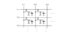
図12は、アクティブマトリクス型の電気泳動装置の回路構成例を説明する図である。図示の電気泳動装置は、複数の走査線と、複数のデータ線が直交して配置され、これらの各交点に電気泳動素子を配置して構成されている。各電気泳動素子は、対向配置される共通電極と画素電極の間に分散系を介在させて構成されている。各電気泳動素子に対する電流供給は走査線及びデータ線に接続されたトランジスタによってなされる。 FIG. 12 is a diagram illustrating a circuit configuration example of an active matrix type electrophoresis apparatus. In the illustrated electrophoresis apparatus, a plurality of scanning lines and a plurality of data lines are arranged orthogonally, and an electrophoresis element is arranged at each of these intersections. Each electrophoretic element is configured by interposing a dispersion system between a common electrode and a pixel electrode arranged to face each other. A current is supplied to each electrophoretic element by transistors connected to the scanning line and the data line.
図13は、図12に示すような構成の電気泳動装置の駆動方法についての従来例を説明する波形図である。図13に示す駆動方法では、画像信号導入期間に先立って、全画素を白表示にリセットするリセット期間が設けられている。このリセット期間においては、全画素の画素電極にはデータ線を介して低電源電位Vss(例えば0V)、共通電極の電位(共通電位)Vcomとしては高電源電位Vdd(例えば+10V)が与えられる。また、その後の画像信号導入期間においては、共通電位Vcomとして低電源電位Vss、各画素電極には各データ線を介して、表示画像の内容に応じた電位が各画素ごとに与えられる。 FIG. 13 is a waveform diagram for explaining a conventional example of a method for driving an electrophoresis apparatus having the configuration shown in FIG. In the driving method shown in FIG. 13, a reset period for resetting all pixels to white display is provided prior to the image signal introduction period. In the reset period, the low power supply potential Vss (for example, 0 V) is applied to the pixel electrodes of all the pixels via the data line, and the high power supply potential Vdd (for example, +10 V) is applied as the common electrode potential (common potential) Vcom. In the subsequent image signal introduction period, a low power supply potential Vss is provided as the common potential Vcom, and a potential corresponding to the content of the display image is applied to each pixel electrode via each data line for each pixel.
図14〜図17は、図13に示す従来例の駆動方法によって駆動された場合における電気泳動粒子の挙動(空間分布)を模式的に説明する図である。図14〜図17では、二粒子系の電気泳動装置であって、白丸で示した粒子(白粒子)がマイナスに帯電し、黒丸で示した粒子(黒粒子)がプラスに帯電している場合における各粒子の挙動が模式的に示されている。 14 to 17 are diagrams schematically illustrating the behavior (spatial distribution) of the electrophoretic particles when driven by the conventional driving method shown in FIG. 14 to 17, a two-particle electrophoresis apparatus in which particles indicated by white circles (white particles) are negatively charged and particles indicated by black circles (black particles) are positively charged. The behavior of each particle in is schematically shown.
例えば、データ線信号X1、走査線信号Y1のそれぞれが供給される画素(1,1)の前画面が白表示、次画面が黒表示、であるとし、その場合の電気泳動粒子の挙動を図14に示す。前画面においては、図14(A)に示すように、共通電位VcomとしてはVss、画素電極にはVL(ほぼ0V)の各電位が与えられ、白表示(より正確には、灰色ぎみの白)がなされる。リセット期間においては、図14(B)に示すように、共通電位VcomとしてはVdd、画素電極にはVssの各電位が与えられ、リセット動作としての白表示(より正確には、より強い白)がなされる。次画面においては、図14(C)に示すように、共通電位VcomとしてVss、画素電極にはVddの各電位が与えられ、黒表示(正確には灰色ぎみの黒)がなされる。このとき、画素(1,1)においては直前のリセット期間において強い白表示がなされているため、その後に黒表示としても各電気泳動粒子が十分に移動することができず、黒レベルが黒くならないという不都合が生じる。 For example, assuming that the previous screen of the pixel (1, 1) to which each of the data line signal X1 and the scanning line signal Y1 is supplied is white and the next screen is black, the behavior of the electrophoretic particles in that case is illustrated. 14 shows. In the previous screen, as shown in FIG. 14A, each potential of Vss is given as the common potential Vcom and V L (nearly 0 V) is given to the pixel electrode, and white display (more precisely, gray-out) White) is made. In the reset period, as shown in FIG. 14B, the common potential Vcom is supplied with Vdd, and the pixel electrode is supplied with Vss, and white display is performed as a reset operation (more precisely, stronger white). Is made. In the next screen, as shown in FIG. 14C, the common potential Vcom is Vss and the pixel electrode is Vdd, and black display (accurately, grayish black) is performed. At this time, in the pixel (1, 1), since strong white display is performed in the immediately preceding reset period, each electrophoretic particle cannot move sufficiently even after black display, and the black level does not become black. The inconvenience arises.
データ線信号X1、走査線信号Y2のそれぞれが供給される画素(1,2)の前画面が白表示、次画面も白表示、であるとし、その場合の電気泳動粒子の挙動を図15に示す。前画面においては、図15(A)に示すように、共通電位VcomとしてVss、画素電極にはVL(ほぼ0V)の各電位が与えられ、白表示(より正確には、灰色ぎみの白表示)がなされる。リセット期間においては、図15(B)に示すように、共通電位VcomとしてはVdd、画素電極にはVssの各電位が与えられ、リセット動作としての白表示(より正確には、より強い白表示)がなされる。次画面においては、図15(C)に示すように、共通電位VcomとしてはVss、画素電極にはVddの各電位が与えられ、白表示がなされる。このとき、各電気泳動粒子が必要以上に移動することから白表示がより強い白となってしまい、他の画素との間で相対的に輝度差を生じ、視覚的に残像を生じさせてしまうという不都合が生じる。また、白表示が更に連続した場合には、白粒子が共通電極側、黒粒子が画素電極側にそれぞれ固定されてしまい、次に黒表示となった際に各粒子が移動しにくくなり、良好な黒表示が行えなくなる。また、白表示の際には各電極間に電位差がないので、各粒子が次第に拡散してしまい、白表示が徐々に灰色表示となってしまう。 It is assumed that the previous screen of the pixel (1, 2) supplied with the data line signal X1 and the scanning line signal Y2 is white and the next screen is also white, and the behavior of the electrophoretic particles in that case is shown in FIG. Show. In the previous screen, as shown in FIG. 15A, the common potential Vcom is Vss, and the pixel electrode is given a potential of V L (approximately 0 V), and white display (more precisely, grayish white) Display). In the reset period, as shown in FIG. 15B, the common potential Vcom is supplied with Vdd, and the pixel electrode is supplied with Vss potential, so that white display as a reset operation (more precisely, stronger white display) ) Is made. In the next screen, as shown in FIG. 15C, each potential of Vss is given as the common potential Vcom and Vdd is given to the pixel electrode, and white display is performed. At this time, since each electrophoretic particle moves more than necessary, white display becomes stronger white, which causes a luminance difference relative to other pixels and causes an afterimage visually. The inconvenience arises. In addition, when the white display continues further, the white particles are fixed on the common electrode side and the black particles are fixed on the pixel electrode side, respectively. Black display cannot be performed. In addition, since there is no potential difference between the electrodes during white display, each particle gradually diffuses, and the white display gradually becomes gray.
データ線信号X2、走査線信号Y1のそれぞれが供給される画素(2,1)の前画面が黒表示、次画面は白表示、であるとし、その場合の電気泳動粒子の挙動を図16に示す。前画面においては、図16(A)に示すように、共通電位VcomとしてはVss、画素電極にはVH(8V程度)の各電位が与えられ、黒表示(より正確には、白色ぎみの黒表示)がなされる。リセット期間においては、図16(B)に示すように、共通電位VcomとしてはVdd、画素電極にはVssの各電位が与えられ、リセット動作としての白表示(より正確には、灰色ぎみの白表示)がなされる。次画面においては、図16(C)に示すように、共通電位VcomとしてはVss、画素電極にもVssの各電位が与えられ、白表示がなされる。このとき、各電気泳動粒子が必要十分に移動できないことから、次画面の白表示が黒ぎみの白表示となってしまい、他の画素との間で相対的に輝度差を生じ、視覚的に残像を生じさせてしまうという不都合が生じる。具体的には、上述した画素(1,2)との間で白レベルに差が生じてしまう。 The behavior of the electrophoretic particles in this case is shown in FIG. 16 assuming that the previous screen of the pixel (2, 1) to which the data line signal X2 and the scanning line signal Y1 are supplied is black and the next screen is white. Show. In the previous screen, as shown in FIG. 16A, each potential of Vss is given as the common potential Vcom and V H (about 8V) is given to the pixel electrode, and black display (more precisely, white-spotted) (Black display) is made. In the reset period, as shown in FIG. 16B, each potential of Vdd is applied to the common potential Vcom and Vss is applied to the pixel electrode, and white display as a reset operation (more precisely, grayish white Display). In the next screen, as shown in FIG. 16C, the common potential Vcom is Vss, and the pixel electrode is also supplied with the potential Vss, and white display is performed. At this time, since each electrophoretic particle cannot move sufficiently and sufficiently, the white display on the next screen becomes a blackish white display, which causes a relative luminance difference with other pixels and visually. There is a disadvantage that an afterimage is generated. Specifically, a difference in white level occurs between the pixel (1, 2) described above.
データ線信号X2、走査線信号Y2のそれぞれが供給される画素(2,2)の前画面が黒表示、次画面も黒表示、であるとし、その場合の電気泳動粒子の挙動を図17に示す。前画面においては、図17(A)に示すように、共通電位VcomとしてはVss、画素電極にはVH(8V程度)の各電位が与えられ、黒表示(より正確には、白色ぎみの黒表示)がなされる。リセット期間においては、図17(B)に示すように、共通電位VcomとしてはVdd、画素電極にはVssの各電位が与えられ、リセット動作としての白表示(より正確には、灰色ぎみの白表示)がなされる。次画面においては、図17(C)に示すように、共通電位VcomとしてはVss、画素電極にはVddの各電位が与えられ、黒表示がなされる。このとき、各電気泳動粒子は比較的に十分に移動できるので、次画面の黒表示は適切な輝度となるが、上述した画素(1,1)との間では黒レベルに差が生じてしまうという不都合が生じる。 It is assumed that the previous screen of the pixel (2, 2) supplied with the data line signal X2 and the scanning line signal Y2 is black and the next screen is black, and the behavior of the electrophoretic particles in that case is shown in FIG. Show. In the previous screen, as shown in FIG. 17A, each potential of Vss is given as the common potential Vcom and V H (about 8V) is given to the pixel electrode, and black display (more accurately, white-spotted) (Black display) is made. In the reset period, as shown in FIG. 17B, the common potential Vcom is supplied with Vdd, and the pixel electrode is supplied with Vss, and white display as a reset operation (more precisely, grayish white Display). In the next screen, as shown in FIG. 17C, the common potential Vcom is given as Vss, and the pixel electrode is given as Vdd and black is displayed. At this time, since each electrophoretic particle can move relatively sufficiently, the black display on the next screen has an appropriate luminance, but there is a difference in the black level from the pixel (1, 1) described above. The inconvenience arises.
このように、従来例の駆動方法では種々の不都合があり、電気泳動装置の画質を向上させることが難しかった。 As described above, the conventional driving method has various disadvantages, and it is difficult to improve the image quality of the electrophoresis apparatus.
そこで、本発明は、電気泳動装置の画質を向上させることを可能とする技術を提供することを目的とする。 Therefore, an object of the present invention is to provide a technique that can improve the image quality of an electrophoresis apparatus.
第1の態様の本発明は、電気泳動粒子を含有する分散系を共通電極と画素電極との間に介在させてなる電気泳動素子と、上記共通電極と上記画素電極との間に電圧を印加して上記電気泳動素子を駆動する駆動手段と、上記駆動手段を制御する制御手段と、を備える電気泳動装置の駆動方法であって、画像書き換えを行うために、上記制御手段により上記駆動手段を制御して上記共通電極と上記画素電極に電圧を与える画像書き換え期間は、リセット期間と、当該リセット期間の後に設けられる画像信号導入期間とを含み、上記リセット期間は、中間階調よりも高輝度の第1の階調に相当する電圧を上記共通電極と上記画素電極との間に与え、当該電圧によって上記電気泳動粒子を移動させる第1リセット期間と、中間階調よりも低輝度の第2の階調と上記第1の階調との間に含まれる第3の階調に相当する電圧を上記共通電極と上記画素電極との間に与え、当該電圧によって上記電気泳動粒子を移動させる第2リセット期間と、を含むことを特徴とする電気泳動装置の駆動方法である。 According to the first aspect of the present invention, a voltage is applied between an electrophoretic element in which a dispersion system containing electrophoretic particles is interposed between a common electrode and a pixel electrode, and the common electrode and the pixel electrode. An electrophoretic device driving method comprising: a driving unit that drives the electrophoretic element; and a control unit that controls the driving unit. The control unit controls the driving unit to rewrite an image. The image rewriting period for controlling and applying a voltage to the common electrode and the pixel electrode includes a reset period and an image signal introduction period provided after the reset period, and the reset period has higher luminance than the intermediate gradation. A voltage corresponding to the first gradation is applied between the common electrode and the pixel electrode, and a first reset period in which the electrophoretic particles are moved by the voltage, and a second brightness lower than the intermediate gradation. A voltage corresponding to a third gradation included between the gradation and the first gradation is applied between the common electrode and the pixel electrode, and the electrophoretic particles are moved by the voltage. A method for driving an electrophoretic device, comprising: a reset period.
かかる駆動方法によれば、第1リセット期間における1回目のリセット動作の後に中間的な階調に相当する第2のリセット動作がなされることにより、電気泳動粒子が動きやすい状態にすることができるので、前画面と次画面の表示内容(階調)の如何によらず、各電気泳動粒子を適切な分布状態に制御することができる。従って、各画素の階調表現が適切となり、画質を向上させることが可能となる。 According to such a driving method, the second reset operation corresponding to the intermediate gradation is performed after the first reset operation in the first reset period, so that the electrophoretic particles can move easily. Therefore, each electrophoretic particle can be controlled to an appropriate distribution state regardless of the display content (gradation) of the previous screen and the next screen. Therefore, the gradation expression of each pixel becomes appropriate, and the image quality can be improved.
上述した第1リセット期間においては、最高輝度に相当する電圧を上記第1の階調に相当する電圧として印加し、第2リセット期間においては、中間階調よりも低く上記第2の階調よりも高い輝度に相当する電圧を上記第3の階調に相当する電圧として印加することが好ましい。 In the first reset period, a voltage corresponding to the maximum luminance is applied as a voltage corresponding to the first gradation, and in the second reset period, the voltage is lower than the intermediate gradation and lower than the second gradation. It is preferable to apply a voltage corresponding to a high luminance as a voltage corresponding to the third gradation.
これにより、いわゆる白リセット等、全画素を高輝度な状態とする第1リセット動作の際の電気泳動粒子の移動方向と、第2リセット動作の際の電気泳動粒子の移動方向とが逆方向となり、第2リセット動作をより効果的に行うことが可能となる。 As a result, the moving direction of the electrophoretic particles during the first reset operation in which all pixels are in a high luminance state, such as so-called white reset, and the moving direction of the electrophoretic particles during the second reset operation are reversed. The second reset operation can be performed more effectively.
より具体的には、上記第1リセット期間における上記第1の階調に相当する電圧は、上記共通電極に高電源電位Vddを与えるとともに上記画素電極に上記高電源電位Vddよりも低い共通電位Vcを与えることにより実現され、上記第2リセット期間における上記第3の階調に相当する電圧は、上記共通電極に上記共通電位Vcを与えるとともに上記画素電極に上記共通電位Vcより高く、且つ上記高電源電位Vddよりも低いリセット電位VRHを与えることにより実現されることが好ましい。 More specifically, the voltage corresponding to the first gradation in the first reset period applies the high power supply potential Vdd to the common electrode and the common potential Vc lower than the high power supply potential Vdd to the pixel electrode. And a voltage corresponding to the third gradation in the second reset period is applied to the common electrode with the common potential Vc, is higher than the common potential Vc to the pixel electrode, and is high. This is preferably realized by applying a reset potential VRH lower than the power supply potential Vdd.
高電源電位や共通電位を利用することにより、第1の階調に相当する電圧及び第3の階調に相当する電圧として適切な電圧を容易に生成し得る。 By using the high power supply potential or the common potential, it is possible to easily generate appropriate voltages as the voltage corresponding to the first gradation and the voltage corresponding to the third gradation.
また、上記画像信号導入期間は、上記共通電極に所定の共通電位Vcを与えるとともに、当該共通電位Vcを基準として相対的に正の電位又は負の電位を上記画素電極に与えることによって画像書き込みを行うことが好ましい。より具体的には、上記共通電位Vcを高電源電位Vddよりも低く低電源電位Vssよりも高い電位(すなわちVss<Vc<Vddの条件を満たす電位)とし、上記画素電極に与える電位をVDH(VDH>Vc)又はVDL(VDL<Vc)とするとよい。VDH及びVDLは、例えばVDH=Vdd、VDL=Vssとすることができる。 In the image signal introduction period, a predetermined common potential Vc is applied to the common electrode, and image writing is performed by applying a relatively positive potential or a negative potential to the pixel electrode with reference to the common potential Vc. Preferably it is done. More specifically, the common potential Vc is set to a potential lower than the high power supply potential Vdd and higher than the low power supply potential Vss (that is, a potential satisfying the condition of Vss <Vc < Vdd ), and the potential applied to the pixel electrode is V DH (V DH > Vc) or V DL (V DL <Vc) is preferable. For example, V DH and V DL may be V DH = Vdd and V DL = Vss.
これにより、高輝度階調(例えば白表示)の場合又は低輝度階調の場合にも、画素電極と共通電極の間に電位差が残るので、電気泳動粒子の拡散を抑制し、階調を適切に維持することが可能となる。 As a result, even in the case of high luminance gradation (for example, white display) or low luminance gradation, a potential difference remains between the pixel electrode and the common electrode. Can be maintained.
上記共通電位Vcは、高電源電位Vddと低電源電位Vssとの中間電位(Vdd+Vss)/2とすると好適である。 The common potential Vc is preferably an intermediate potential (Vdd + Vss) / 2 between the high power supply potential Vdd and the low power supply potential Vss.
これにより、共通電位Vcを容易に生成することができる。 Thereby, the common potential Vc can be easily generated.
また、電気泳動装置には、一方の電極が上記共通電極と接続され、他方の電極が上記画素電極と接続されてなる保持容量が更に備わっていることが好ましい。 The electrophoresis apparatus preferably further includes a storage capacitor in which one electrode is connected to the common electrode and the other electrode is connected to the pixel electrode.
これにより、共通電極の電位をより安定させることが可能となり、電気泳動素子に印加される電圧をより安定させることができる。 Thereby, the potential of the common electrode can be further stabilized, and the voltage applied to the electrophoretic element can be further stabilized.
第2の態様の本発明は、電気泳動粒子を含有する分散系を共通電極と画素電極との間に介在させてなる電気泳動素子と、上記共通電極と上記画素電極との間に電圧を印加して上記電気泳動素子を駆動する駆動手段と、上記駆動手段を制御する制御手段と、を備える電気泳動装置の駆動方法であって、画像書き換えを行うために、上記制御手段により上記駆動手段を制御して上記共通電極と上記画素電極に電圧を与える画像書き換え期間は、リセット期間と、当該リセット期間の後に設けられる画像信号導入期間とを含み、上記リセット期間は、中間階調よりも低輝度の第1の階調に相当する電圧を上記共通電極と上記画素電極との間に与え、当該電圧によって上記電気泳動粒子を移動させる第1リセット期間と、中間階調よりも高輝度の第2の階調と上記第1の階調との間に含まれる第3の階調に相当する電圧を上記共通電極と上記画素電極との間に与え、当該電圧によって上記電気泳動粒子を移動させる第2リセット期間と、を含むことを特徴とする電気泳動装置の駆動方法である。 In the second aspect of the present invention, a voltage is applied between the electrophoretic element having a dispersion system containing electrophoretic particles interposed between the common electrode and the pixel electrode, and the common electrode and the pixel electrode. An electrophoretic device driving method comprising: a driving unit that drives the electrophoretic element; and a control unit that controls the driving unit. The control unit controls the driving unit to rewrite an image. The image rewriting period for controlling and applying a voltage to the common electrode and the pixel electrode includes a reset period and an image signal introduction period provided after the reset period. The reset period has a lower luminance than the intermediate gradation. A voltage corresponding to the first gradation is applied between the common electrode and the pixel electrode, and the electrophoretic particles are moved by the voltage, and the second brightness is higher than the intermediate gradation. A voltage corresponding to a third gradation included between the gradation and the first gradation is applied between the common electrode and the pixel electrode, and the electrophoretic particles are moved by the voltage. A method for driving an electrophoretic device, comprising: a reset period.
かかる駆動方法においても、第1リセット期間における1回目のリセット動作の後に中間的な階調に相当する第2のリセット動作がなされることにより、電気泳動粒子が動きやすい状態にすることができるので、前画面と次画面の表示内容(階調)の如何によらず、各電気泳動粒子を適切な分布状態に制御することができる。従って、各画素の階調表現が適切となり、画質を向上させることが可能となる。 Also in this driving method, the second reset operation corresponding to the intermediate gradation is performed after the first reset operation in the first reset period, so that the electrophoretic particles can be easily moved. Regardless of the display content (gradation) of the previous screen and the next screen, each electrophoretic particle can be controlled to an appropriate distribution state. Therefore, the gradation expression of each pixel becomes appropriate, and the image quality can be improved.
上述した第1リセット期間においては、最低輝度に相当する電圧を上記第1の階調に相当する電圧として印加し、第2リセット期間においては、中間階調よりも高く上記第2の階調よりも低い輝度に相当する電圧を上記第3の階調に相当する電圧として印加することが好ましい。 In the first reset period, a voltage corresponding to the lowest luminance is applied as a voltage corresponding to the first gradation, and in the second reset period, the voltage is higher than the intermediate gradation and higher than the second gradation. It is preferable to apply a voltage corresponding to low luminance as a voltage corresponding to the third gradation.
これにより、いわゆる黒リセット等、全画素を低輝度な状態とする第1リセット動作の際の電気泳動粒子の移動方向と、第2リセット動作の際の電気泳動粒子の移動方向とが逆方向となり、第2リセット動作をより効果的に行うことが可能となる。 As a result, the moving direction of the electrophoretic particles during the first reset operation in which all pixels are in a low luminance state, such as so-called black reset, and the moving direction of the electrophoretic particles during the second reset operation are reversed. The second reset operation can be performed more effectively.
より具体的には、上記第1リセット期間における上記第1の階調に相当する電圧は、上記共通電極に低電源電位Vssを与えるとともに上記画素電極に上記低電源電位Vssよりも高い共通電位Vcを与えることにより実現され、上記第2リセット期間における上記第3の階調に相当する電圧は、上記共通電極に上記共通電位Vcを与えるとともに上記画素電極に上記共通電位Vcより低く、且つ上記低電源電位Vssよりも高いリセット電位VRLを与えることにより実現されることが好ましい。 More specifically, the voltage corresponding to the first gradation in the first reset period applies the low power supply potential Vss to the common electrode and the common potential Vc higher than the low power supply potential Vss to the pixel electrode. And a voltage corresponding to the third gradation in the second reset period is applied to the common electrode with the common potential Vc, is lower than the common potential Vc to the pixel electrode, and is low. It is preferable that the reset potential V RL be higher than the power supply potential Vss.
低電源電位や共通電位を利用することにより、第1の階調に相当する電圧及び第3の階調に相当する電圧として適切な電圧を容易に生成し得る。 By using the low power supply potential or the common potential, it is possible to easily generate appropriate voltages as the voltage corresponding to the first gradation and the voltage corresponding to the third gradation.
また、上記画像信号導入期間は、上記共通電極に所定の共通電位Vcを与えるとともに、当該共通電位Vcを基準として相対的に正の電位又は負の電位を上記画素電極に与えることによって画像書き込みを行うことが好ましい。より具体的には、上記共通電位Vcを高電源電位Vddよりも低く低電源電位Vssよりも高い電位(すなわちVss<Vc<Vddの条件を満たす電位)とし、上記画素電極に与える電位をVDH(VDH>Vc)又はVDL(VDL<Vc)とするとよい。VDH及びVDLは、例えばVDH=Vdd、VDL=Vssとすることができる。 In the image signal introduction period, a predetermined common potential Vc is applied to the common electrode, and image writing is performed by applying a relatively positive potential or a negative potential to the pixel electrode with reference to the common potential Vc. Preferably it is done. More specifically, the common potential Vc is set to a potential lower than the high power supply potential Vdd and higher than the low power supply potential Vss (that is, a potential satisfying the condition of Vss <Vc < Vdd ), and the potential applied to the pixel electrode is V DH (V DH > Vc) or V DL (V DL <Vc) is preferable. For example, V DH and V DL may be V DH = Vdd and V DL = Vss.
これにより、低輝度階調(例えば黒表示)の場合又は高輝度階調の場合にも、画素電極と共通電極の間に電位差が残るので、電気泳動粒子の拡散を抑制し、階調を適切に維持することが可能となる。 As a result, even in the case of low luminance gradation (for example, black display) or high luminance gradation, a potential difference remains between the pixel electrode and the common electrode. Can be maintained.
上記共通電位Vcは、高電源電位Vddと低電源電位Vssとの中間電位(Vdd+Vss)/2とすると好適である。 The common potential Vc is preferably an intermediate potential (Vdd + Vss) / 2 between the high power supply potential Vdd and the low power supply potential Vss.
これにより、共通電位Vcを容易に生成することができる。 Thereby, the common potential Vc can be easily generated.
また、電気泳動装置には、一方の電極が上記共通電極と接続され、他方の電極が上記画素電極と接続されてなる保持容量が更に備わっていることが好ましい。 The electrophoresis apparatus preferably further includes a storage capacitor in which one electrode is connected to the common electrode and the other electrode is connected to the pixel electrode.
これにより、共通電極の電位をより安定させることが可能となり、電気泳動素子に印加される電圧をより安定させることができる。 Thereby, the potential of the common electrode can be further stabilized, and the voltage applied to the electrophoretic element can be further stabilized.
第3の態様の本発明は、電気泳動粒子を含有する分散系を共通電極と画素電極との間に介在させてなる電気泳動素子と、上記共通電極と上記画素電極との間に電圧を印加して上記電気泳動素子を駆動する駆動手段と、上記駆動手段を制御する制御手段と、を備え、画像書き換えを行うために上記駆動手段が上記共通電極と上記画素電極に電圧を与える画像書き換え期間には、リセット期間と、当該リセット期間の後に設けられる画像信号導入期間とが含まれ、上記リセット期間は、中間階調よりも高輝度の第1の階調に相当する電圧を上記共通電極と上記画素電極との間に与え、当該電圧によって上記電気泳動粒子を移動させる第1リセット期間と、中間階調よりも低輝度の第2の階調と、上記第1の階調との間に含まれる第3の階調に相当する電圧を上記共通電極と上記画素電極との間に与え、当該電圧によって上記電気泳動粒子を移動させる第2リセット期間と、を含むことを特徴とする電気泳動装置である。 In the third aspect of the present invention, a voltage is applied between the electrophoretic element having a dispersion system containing electrophoretic particles interposed between the common electrode and the pixel electrode, and the common electrode and the pixel electrode. And an image rewriting period in which the driving means applies a voltage to the common electrode and the pixel electrode in order to perform image rewriting, and a driving means for driving the electrophoretic element and a control means for controlling the driving means. Includes a reset period and an image signal introduction period provided after the reset period. In the reset period, a voltage corresponding to a first gradation higher in luminance than the intermediate gradation is applied to the common electrode. Between the first reset period which is applied between the pixel electrode and moves the electrophoretic particles by the voltage, the second gradation having a lower luminance than the intermediate gradation, and the first gradation Corresponds to the 3rd gradation included That the voltage applied between the common electrode and the pixel electrodes, an electrophoresis apparatus which comprises a second reset period for moving the electrophoretic particles by the voltage.
かかる構成によれば、各画素の階調表現が適切となり、画質を向上させることが可能となる。 According to this configuration, the gradation expression of each pixel becomes appropriate, and the image quality can be improved.
上述した制御手段は、上記第1リセット期間において、最高輝度に相当する電圧を上記第1の階調に相当する電圧として印加し、上記第2リセット期間において、中間階調よりも低く上記第2の階調よりも高い輝度に相当する電圧を上記第3の階調に相当する電圧として印加することが好ましい。 The control means applies a voltage corresponding to the highest luminance as a voltage corresponding to the first gradation in the first reset period, and lowers the second gradation lower than the intermediate gradation in the second reset period. It is preferable to apply a voltage corresponding to a higher luminance than the gray level as a voltage corresponding to the third gray level.
これにより、いわゆる白リセット等、全画素を高輝度な状態とする第1リセット動作の際の電気泳動粒子の移動方向と、第2リセット動作の際の電気泳動粒子の移動方向とが逆方向となり、第2リセット動作をより効果的に行うことが可能となる。 As a result, the moving direction of the electrophoretic particles during the first reset operation in which all pixels are in a high luminance state, such as so-called white reset, and the moving direction of the electrophoretic particles during the second reset operation are reversed. The second reset operation can be performed more effectively.
より具体的には、上記制御手段は、上記第1リセット期間における上記第1の階調に相当する電圧を、上記共通電極に高電源電位Vddを与えるとともに上記画素電極に上記高電源電位Vddよりも低い共通電位Vcを与えることにより実現し、上記第2リセット期間における上記第3の階調に相当する電圧を、上記共通電極に上記共通電位Vcを与えるとともに上記画素電極に上記共通電位Vcより高く、且つ上記高電源電位Vddよりも低いリセット電位VRHを与えることにより実現することが好ましい。 More specifically, the control means applies a voltage corresponding to the first gradation in the first reset period to the high power supply potential Vdd to the common electrode and from the high power supply potential Vdd to the pixel electrode. And a voltage corresponding to the third gradation in the second reset period is applied to the common electrode from the common potential Vc and the pixel electrode is supplied with the common potential Vc. This is preferably realized by applying a reset potential V RH that is high and lower than the high power supply potential Vdd.
高電源電位や共通電位を利用することにより、第1の階調に相当する電圧及び第3の階調に相当する電圧として適切な電圧を容易に生成し得る。 By using the high power supply potential or the common potential, it is possible to easily generate appropriate voltages as the voltage corresponding to the first gradation and the voltage corresponding to the third gradation.
また、上記制御手段は、上記画像信号導入期間において、上記共通電極に所定の共通電位Vcを与えるとともに、当該共通電位Vcを基準として相対的に正の電位又は負の電位を上記画素電極に与えることによって画像書き込みを行うことが好ましい。より具体的には、制御手段は、上記共通電位Vcを高電源電位Vddよりも低く低電源電位Vssよりも高い電位(すなわちVss<Vc<Vddの条件を満たす電位)とし、上記画素電極に与える電位をVDH(VDH>Vc)又はVDL(VDL<Vc)とするとよい。VDH及びVDLは、例えばVDH=Vdd、VDL=Vssとすることができる。 The control means applies a predetermined common potential Vc to the common electrode and supplies a relatively positive potential or a negative potential to the pixel electrode with reference to the common potential Vc during the image signal introduction period. Thus, it is preferable to perform image writing. More specifically, the control means sets the common potential Vc to a potential lower than the high power supply potential Vdd and higher than the low power supply potential Vss (that is, a potential that satisfies the condition of Vss <Vc < Vdd ) and applies the same to the pixel electrode. The potential may be V DH (V DH > Vc) or V DL (V DL <Vc). For example, V DH and V DL may be V DH = Vdd and V DL = Vss.
これにより、高輝度階調(例えば白表示)の場合又は低輝度階調の場合にも、画素電極と共通電極の間に電位差が残るので、電気泳動粒子の拡散を抑制し、階調を適切に維持することが可能となる。 As a result, even in the case of high luminance gradation (for example, white display) or low luminance gradation, a potential difference remains between the pixel electrode and the common electrode. Can be maintained.
上記共通電位Vcは、高電源電位Vddと低電源電位Vssとの中間電位(Vdd+Vss)/2とすると好適である。 The common potential Vc is preferably an intermediate potential (Vdd + Vss) / 2 between the high power supply potential Vdd and the low power supply potential Vss.
これにより、共通電位Vcを容易に生成することができる。 Thereby, the common potential Vc can be easily generated.
また、電気泳動装置には、一方の電極が上記共通電極と接続され、他方の電極が上記画素電極と接続されてなる保持容量が更に備わっていることが好ましい。 The electrophoresis apparatus preferably further includes a storage capacitor in which one electrode is connected to the common electrode and the other electrode is connected to the pixel electrode.
これにより、共通電極の電位をより安定させることが可能となり、電気泳動素子に印加される電圧をより安定させることができる。 Thereby, the potential of the common electrode can be further stabilized, and the voltage applied to the electrophoretic element can be further stabilized.
第4の態様の本発明は、電気泳動粒子を含有する分散系を共通電極と画素電極との間に介在させてなる電気泳動素子と、上記共通電極と上記画素電極との間に電圧を印加して上記電気泳動素子を駆動する駆動手段と、上記駆動手段を制御する制御手段と、を備え、画像書き換えを行うために上記駆動手段が上記共通電極と上記画素電極に電圧を与える画像書き換え期間には、リセット期間と、当該リセット期間の後に設けられる画像信号導入期間とが含まれ、上記リセット期間は、中間階調よりも低輝度の第1の階調に相当する電圧を上記共通電極と上記画素電極との間に与え、当該電圧によって上記電気泳動粒子を移動させる第1リセット期間と、中間階調よりも高輝度の第2の階調と、上記第1の階調との間に含まれる第3の階調に相当する電圧を上記共通電極と上記画素電極との間に与え、当該電圧によって上記電気泳動粒子を移動させる第2リセット期間と、を含むことを特徴とする電気泳動装置である。 According to the fourth aspect of the present invention, a voltage is applied between the electrophoretic element in which a dispersion system containing electrophoretic particles is interposed between the common electrode and the pixel electrode, and the common electrode and the pixel electrode. And an image rewriting period in which the driving means applies a voltage to the common electrode and the pixel electrode in order to perform image rewriting, and a driving means for driving the electrophoretic element and a control means for controlling the driving means. Includes a reset period and an image signal introduction period provided after the reset period. In the reset period, a voltage corresponding to the first gradation having a lower luminance than the intermediate gradation is applied to the common electrode. Between the first reset period that is applied between the pixel electrode and moves the electrophoretic particles by the voltage, the second gradation that is brighter than the intermediate gradation, and the first gradation Corresponds to the 3rd gradation included That the voltage applied between the common electrode and the pixel electrodes, an electrophoresis apparatus which comprises a second reset period for moving the electrophoretic particles by the voltage.
かかる構成によっても、各画素の階調表現が適切となり、画質を向上させることが可能となる。 Even with such a configuration, the gradation expression of each pixel becomes appropriate, and the image quality can be improved.
上述した制御手段は、上記第1リセット期間において、最低輝度に相当する電圧を上記第1の階調に相当する電圧として印加し、上記第2リセット期間において、中間階調よりも高く上記第2の階調よりも低い輝度に相当する電圧を上記第3の階調に相当する電圧として印加することが好ましい。 The control means applies a voltage corresponding to the minimum luminance as a voltage corresponding to the first gradation in the first reset period, and is higher than the intermediate gradation in the second reset period. It is preferable to apply a voltage corresponding to a lower luminance than the gray level as a voltage corresponding to the third gray level.
これにより、いわゆる黒リセット等、全画素を低輝度な状態とする第1リセット動作の際の電気泳動粒子の移動方向と、第2リセット動作の際の電気泳動粒子の移動方向とが逆方向となり、第2リセット動作をより効果的に行うことが可能となる。 As a result, the moving direction of the electrophoretic particles during the first reset operation in which all pixels are in a low luminance state, such as so-called black reset, and the moving direction of the electrophoretic particles during the second reset operation are reversed. The second reset operation can be performed more effectively.
より具体的には、上記制御手段は、上記第1リセット期間における上記第1の階調に相当する電圧を、上記共通電極に低電源電位Vssを与えるとともに上記画素電極に上記低電源電位Vssよりも高い共通電位Vcを与えることにより実現し、上記第2リセット期間における上記第3の階調に相当する電圧を、上記共通電極に上記共通電位Vcを与えるとともに上記画素電極に上記共通電位Vcより低く、且つ上記低電源電位Vssよりも高いリセット電位VRLを与えることにより実現することが好ましい。 More specifically, the control means applies a voltage corresponding to the first gradation in the first reset period to the common electrode with a low power supply potential Vss and to the pixel electrode with the low power supply potential Vss. And a voltage corresponding to the third gradation in the second reset period is applied to the common electrode from the common potential Vc and the pixel electrode is supplied with the common potential Vc. This is preferably realized by applying a reset potential V RL that is low and higher than the low power supply potential Vss.
低電源電位や共通電位を利用することにより、第1の階調に相当する電圧及び第3の階調に相当する電圧として適切な電圧を容易に生成し得る。 By using the low power supply potential or the common potential, it is possible to easily generate appropriate voltages as the voltage corresponding to the first gradation and the voltage corresponding to the third gradation.
また、上記制御手段は、上記画像信号導入期間において、上記共通電極に所定の共通電位Vcを与えるとともに、当該共通電位Vcを基準として相対的に正の電位又は負の電位を上記画素電極に与えることによって画像書き込みを行うことが好ましい。より具体的には、制御手段は、上記共通電位Vcを高電源電位Vddよりも低く低電源電位Vssよりも高い電位(すなわちVss<Vc<Vddの条件を満たす電位)とし、上記画素電極に与える電位をVDH(VDH>Vc)又はVDL(VDL<Vc)とするとよい。VDH及びVDLは、例えばVDH=Vdd、VDL=Vssとすることができる。 The control means applies a predetermined common potential Vc to the common electrode and supplies a relatively positive potential or a negative potential to the pixel electrode with reference to the common potential Vc during the image signal introduction period. Thus, it is preferable to perform image writing. More specifically, the control means sets the common potential Vc to a potential lower than the high power supply potential Vdd and higher than the low power supply potential Vss (that is, a potential that satisfies the condition of Vss <Vc < Vdd ) and applies the same to the pixel electrode. The potential may be V DH (V DH > Vc) or V DL (V DL <Vc). For example, V DH and V DL may be V DH = Vdd and V DL = Vss.
これにより、低輝度階調(例えば黒表示)の場合又は高輝度階調の場合にも、画素電極と共通電極の間に電位差が残るので、電気泳動粒子の拡散を抑制し、階調を適切に維持することが可能となる。 As a result, even in the case of low luminance gradation (for example, black display) or high luminance gradation, a potential difference remains between the pixel electrode and the common electrode. Can be maintained.
上記共通電位Vcは、高電源電位Vddと低電源電位Vssとの中間電位(Vdd+Vss)/2とすると好適である。 The common potential Vc is preferably an intermediate potential (Vdd + Vss) / 2 between the high power supply potential Vdd and the low power supply potential Vss.
これにより、共通電位Vcを容易に生成することができる。 Thereby, the common potential Vc can be easily generated.
また、電気泳動装置には、一方の電極が上記共通電極と接続され、他方の電極が上記画素電極と接続されてなる保持容量が更に備わっていることが好ましい。 The electrophoresis apparatus preferably further includes a storage capacitor in which one electrode is connected to the common electrode and the other electrode is connected to the pixel electrode.
これにより、共通電極の電位をより安定させることが可能となり、電気泳動素子に印加される電圧をより安定させることができる。 Thereby, the potential of the common electrode can be further stabilized, and the voltage applied to the electrophoretic element can be further stabilized.
第5の態様の本発明は、上述した電気泳動表示装置を用いて構成される電子機器である。ここで「電子機器」とは、一定の機能を奏する機器一般をいい、その構成に特に限定が無いが、例えば、電子ペーパ、電子ブック、ICカード、PDA、電子手帳等が含まれる。 The fifth aspect of the present invention is an electronic apparatus configured using the electrophoretic display device described above. Here, “electronic device” refers to a general device having a certain function, and its configuration is not particularly limited, and includes, for example, an electronic paper, an electronic book, an IC card, a PDA, an electronic notebook, and the like.
これにより、表示部の画質に優れた電子機器が得られる。 As a result, an electronic device having excellent image quality of the display unit can be obtained.
以下、本発明の実施の形態について図面を参照しながら説明する。 Hereinafter, embodiments of the present invention will be described with reference to the drawings.
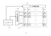
図1は、一実施形態の電気泳動表示装置の回路構成を概略的に説明するブロック図である。図1に示す本実施形態の電気泳動表示装置1は、コントローラ11、表示部12、走査線駆動回路13、データ線駆動回路14を含んで構成されている。
FIG. 1 is a block diagram schematically illustrating a circuit configuration of an electrophoretic display device according to an embodiment. The
コントローラ11は、走査線駆動回路13及びデータ線駆動回路14を制御するものであり、図示しない画像信号処理回路やタイミングジェネレータなどを含んで構成されている。このコントローラ11は、表示部12に表示させる画像を示す画像信号(画像データ)、画像書き換え時のリセットを行うためのリセットデータ、その他各種信号(クロック信号等)を生成し、走査線駆動回路13又はデータ線駆動回路14へ出力する。
The controller 11 controls the scanning
表示部12は、X方向に沿って平行に配列された複数本のデータ線と、Y方向に沿って平行に配列された複数本の走査線と、これらのデータ線と走査線の各交点に配置される画素回路とを備えており、各画素回路に含まれる電気泳動素子によって画像表示を行うものである。
The
走査線駆動回路13は、表示部12の各走査線と接続されており、これらの走査線のいずれかを選択し、当該選択した走査線に所定の走査線信号Y1、Y2、…、Ymを供給する。この走査線信号Y1、Y2、…、Ymは、アクティブ期間(Hレベル期間)が順次シフトする信号となっており、各走査線に出力されることにより、各走査線に接続された画素回路が順次オン状態とされる。
The scanning
データ線駆動回路14は、表示部12の各データ線と接続されており、走査線駆動回路13によって選択された各画素回路に対してデータ信号X1、X2、…、Xnを供給する。
The data line driving
なお、上述したコントローラ11が本発明における「制御手段」に相当し、走査線駆動回路13及びデータ線駆動回路14が本発明における「駆動手段」に相当する。
The controller 11 described above corresponds to the “control unit” in the present invention, and the scanning
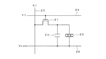
図2は、各画素回路の構成を説明する回路図である。図2に示す画素回路は、スイッチング用のトランジスタ21、電気泳動素子22、保持容量23を含んで構成されている。トランジスタ21は、例えばNチャネルトランジスタであって、そのゲートが走査線24に接続され、ソースがデータ線25に接続され、ドレインが電気泳動素子22の画素電極に接続されている。電気泳動素子22は、各画素ごとに設けられる画素電極と、各画素共通に用いられる共通電極26との間に分散系を介在させて構成されている。保持容量23は、電気泳動素子22と並列に接続されている。より具体的には、保持容量23は、一方の電極がトランジスタのソースに接続され、他方の電極が共通電極26に接続されている。
FIG. 2 is a circuit diagram illustrating the configuration of each pixel circuit. The pixel circuit shown in FIG. 2 includes a switching
図3は、電気泳動素子の構成例を説明する模式断面図である。図3に示すように本実施形態の電気泳動素子22は、ガラス又は樹脂等からなる基板31上に形成された画素電極33と、ガラス又は樹脂等からなる基板32上に形成された共通電極34との間に、電気泳動素子36、37を含有する分散系35を介在させて構成されている。本実施形態では、電気泳動素子36は電気的にマイナスに帯電した白色の粒子(白粒子)であり、電気泳動素子37は電気的にプラスに帯電した黒色の粒子(黒粒子)であるものとする。画素電極33と共通電極34の間に印加する電圧を制御することにより、これらの電気泳動粒子36、37の空間的配置を変化させ、各画素を白色から黒色まで階調変化させて画像表示がなされる。
FIG. 3 is a schematic cross-sectional view illustrating a configuration example of the electrophoretic element. As shown in FIG. 3, the
本実施形態の電気泳動表示装置1はこのような構成を有しており、次に当該電気泳動表示装置1における各電気泳動素子の駆動方法について説明する。
The
図4は、本実施形態の電気泳動表示装置1における各電気泳動素子の駆動方法について説明する波形図である。本実施形態の電気泳動表示装置1においては、画像書き換えを行うために、コントローラ11により走査線駆動回路13及びデータ線駆動回路14を制御し、各電気泳動素子22の共通電極と画素電極に電圧を与える画像書き換え期間には、リセット期間と、当該リセット期間の後に設けられる画像信号導入期間とが含まれる。そして、図示のようにリセット期間には、中間階調よりも高輝度の第1の階調に相当する電圧を共通電極と画素電極との間に与え、当該電圧によって電気泳動粒子を移動させる第1リセット期間r1と、中間階調よりも低輝度の第2の階調と第1の階調との間に含まれる第3の階調に相当する電圧を共通電極と画素電極との間に与え、当該電圧によって電気泳動粒子を移動させる第2リセット期間r2が含まれる。
FIG. 4 is a waveform diagram illustrating a method for driving each electrophoretic element in the
ここで、リセット期間は、電気泳動素子22の応答時間τの0.5倍(0.5τ)から2倍(2τ)の範囲内に設定することが望ましい。一般に、リセット期間が0.5τよりも短いと電気泳動粒子の電気泳動が不十分となり、リセットが十分に効かない一方で、2τよりも長いと視覚的にちらつきを生じさせるからである。また、第2リセット期間r2は、リセット期間全体の40%〜60%程度に設定することが望ましい。第2リセット期間がリセット期間全体の40%よりも長いと画素の階調が白色から灰色へとなるように電気泳動粒子が動き始める一方、60%よりも短いと第1リセット期間r1において白色に画像消却が可能となるからである。
Here, it is desirable to set the reset period within the range of 0.5 times (0.5τ) to 2 times (2τ) of the response time τ of the
本実施形態では、第1リセット期間r1においては第1の階調に相当する電圧として、最高輝度(すなわち、最も強い白色)に相当する電圧を印加することにより、全画素を最高階調にリセットする。また、第2リセット期間r2においては第3の階調に相当する電圧として、中間階調よりも低く第2の階調よりも高い輝度に相当する電圧を印加することにより、全画素を中間階調にリセットする。より具体的には、第1リセット期間における第1の階調に相当する電圧は、共通電極に高電源電位Vdd(例えば+10V)を与えるとともに画素電極にVddよりも低い共通電位Vc(例えば+5V)を与えることにより実現される。このとき、画素電極からみた共通電極の電位はVdd−Vcとなる。本実施形態ではVss<Vc<Vddと設定してあるので、Vdd−Vcは正電位となり、負に帯電した粒子(例えば白粒子)は共通電極に引き寄せられる。また、第2リセット期間における第3の階調に相当する電圧は、共通電極に共通電位Vc(例えば+5V)を与えるとともに画素電極に共通電位Vcより高く、且つ高電源電位Vddよりも低いリセット電位VRH、すなわちVc<VRH<Vddの関係を満たす電位(例えば+7.5V)を与えることにより実現される。このとき、画素電極からみた共通電極の電位はVc−VRHとなり、Vc<VRH<VddであるのでVc−VRHは負電位となり、正に帯電した粒子(例えば黒粒子)が共通電極に引き寄せられる。 In the present embodiment, in the first reset period r1, all pixels are reset to the maximum gradation by applying a voltage corresponding to the maximum luminance (that is, the strongest white color) as the voltage corresponding to the first gradation. To do. In the second reset period r2, a voltage corresponding to a luminance lower than the intermediate gradation and higher than the second gradation is applied as a voltage corresponding to the third gradation, so that all pixels are connected to the intermediate gradation. To the key. More specifically, the voltage corresponding to the first gradation in the first reset period applies a high power supply potential Vdd (for example, +10 V) to the common electrode and a common potential Vc (for example, +5 V) lower than Vdd to the pixel electrode. It is realized by giving. At this time, the potential of the common electrode viewed from the pixel electrode is Vdd−Vc. In this embodiment, since Vss <Vc <Vdd is set, Vdd−Vc becomes a positive potential, and negatively charged particles (for example, white particles) are attracted to the common electrode. In addition, the voltage corresponding to the third gradation in the second reset period applies a common potential Vc (for example, + 5V) to the common electrode, and is higher than the common potential Vc to the pixel electrode and lower than the high power supply potential Vdd. This is realized by applying a potential satisfying the relationship of V RH , that is, Vc <V RH <Vdd (for example, +7.5 V). At this time, the potential of the common electrode viewed from the pixel electrode is Vc−V RH and Vc <V RH <Vdd, so Vc−V RH is a negative potential, and positively charged particles (for example, black particles) are applied to the common electrode. Gravitate.
また、画像信号導入期間においては、共通電極に所定の共通電位Vcを与えるとともに、当該共通電位Vcを基準として相対的に正の電位VDH(VDH>Vc)又は負の電位VDL(VDL<Vc)を画素電極に与えることによって画像書き込みを行う。この共通電位Vcは、高電源電位Vddよりも低く低電源電位Vssよりも高い電位(Vss<Vc<Vdd)であればよい。共通電位Vcは、例えば、高電源電位Vdd(例えば+10V)と低電源電位Vss(例えば0V)との中間電位(Vdd+Vss)/2(=+5V)とすることにより、容易に生成することができる。 In the image signal introduction period, a predetermined common potential Vc is given to the common electrode, and a relatively positive potential V DH (V DH > Vc) or a negative potential V DL (V Image writing is performed by applying DL <Vc) to the pixel electrode. The common potential Vc may be a potential lower than the high power supply potential Vdd and higher than the low power supply potential Vss (Vss <Vc <Vdd). The common potential Vc can be easily generated, for example, by setting the intermediate potential (Vdd + Vss) / 2 (= + 5 V) between the high power supply potential Vdd (for example, +10 V) and the low power supply potential Vss (for example, 0 V).
図5〜図8は、本実施形態の駆動方法によって駆動させる電気泳動粒子の挙動を模式的に説明する図であり、図4に例示した駆動波形に対応した各電気泳動素子36、37の挙動が示されている。なお、以下では説明の便宜上、電気泳動素子36(マイナスに帯電)を「白粒子」、電気泳動素子37(プラスに帯電)を「黒粒子」と称する。
5 to 8 are diagrams for schematically explaining the behavior of the electrophoretic particles driven by the driving method of the present embodiment, and the behavior of the
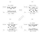
図5は、データ線信号X1、走査線信号Y1のそれぞれが供給される画素(1,1)において、前画面が白表示であり、次画面を黒表示とする場合の電気泳動粒子の挙動を模式的に示している。前画面においては、図5(A)に示すように、共通電位VcomとしてはVc(+5V)、画素電極にはVDL(ほぼ0V)の各電位が与えられ、共通電極(上側電極)に白粒子、画素電極(下側電極)に黒粒子がそれぞれ引き寄せられ、画素(1,1)はほぼ最高輝度の階調、すなわち白表示となる。第1のリセット期間r1においては、図5(B)に示すように、共通電位VcomとしてはVdd(+10V)、画素電極にはVc(+5V)の各電位が与えられる。このとき、白粒子及び黒粒子の分布にはほとんど変化がなく、リセット動作としての白表示がなされる。第2のリセット期間r2においては、図5(C)に示すように、共通電位VcomとしてはVc(+5V)、画素電極にはリセット電位VRH(+7.5V)の各電位が与えられる。このとき、白粒子は画素電極、黒粒子は共通電極にそれぞれ引き寄せられるが、電圧がそれほど高くないため図示のように両粒子が適度に混合した分布状態となり、リセット動作としての中間階調表示がなされる。その後、次画面においては、図5(D)に示すように、共通電位VcomとしてVc(+5V)、画素電極にはVDH(本例ではVdd)の各電位が与えられ、白粒子は画素電極、黒粒子は共通電極にそれぞれ引き寄せられ、画素(1,1)はほぼ最低輝度の階調、すなわち黒表示となる。事前に中間階調表示によるリセット動作がなされることで、各電気泳動粒子が動きやすい状態となるため、前画面の表示内容によらず適切な階調での黒表示が実現される。 FIG. 5 shows the behavior of electrophoretic particles when the previous screen is white display and the next screen is black display in the pixel (1, 1) to which the data line signal X1 and the scanning line signal Y1 are respectively supplied. This is shown schematically. In the previous screen, as shown in FIG. 5A, the common potential Vcom is Vc (+5 V), the pixel electrode is V DL (approximately 0 V), and the common electrode (upper electrode) is white. Black particles are attracted to the particles and the pixel electrode (lower electrode), respectively, and the pixel (1, 1) has a gradation with almost the highest luminance, that is, white display. In the first reset period r1, as shown in FIG. 5B, each potential of Vdd (+10 V) is applied as the common potential Vcom, and Vc (+5 V) is applied to the pixel electrode. At this time, there is almost no change in the distribution of white particles and black particles, and white display is performed as a reset operation. In the second reset period r2, as shown in FIG. 5C, the common potential Vcom is supplied with Vc (+5 V), and the pixel electrode is supplied with the reset potential V RH (+7.5 V). At this time, the white particles are attracted to the pixel electrode and the black particles are attracted to the common electrode, but the voltage is not so high so that both particles are appropriately mixed as shown in the figure, and the intermediate gradation display as the reset operation is performed. Made. Thereafter, on the next screen, as shown in FIG. 5D, each potential of Vc (+5 V) is applied as the common potential Vcom, V DH (Vdd in this example) is applied to the pixel electrode, and the white particles are applied to the pixel electrode. The black particles are attracted to the common electrode, and the pixel (1, 1) has a gradation with the lowest luminance, that is, a black display. By performing the reset operation by the intermediate gradation display in advance, each electrophoretic particle becomes easy to move, so that black display at an appropriate gradation is realized regardless of the display content of the previous screen.
図6は、データ線信号X1、走査線信号Y2のそれぞれが供給される画素(1,2)において、前画面が白表示であり、次画面も白表示とする場合の電気泳動粒子の挙動を模式的に示している。前画面においては、図6(A)に示すように、共通電位VcomとしてはVc(+5V)、画素電極にはVDL(ほぼ0V)の各電位が与えられ、共通電極(上側電極)に白粒子、画素電極(下側電極)に黒粒子がそれぞれ引き寄せられ、画素(1,2)はほぼ最高輝度の階調、すなわち白表示となる。第1のリセット期間r1においては、図6(B)に示すように、共通電位VcomとしてはVdd(+10V)、画素電極にはVc(+5V)の各電位が与えられる。このとき、白粒子及び黒粒子の分布にはほとんど変化がなく、リセット動作としての白表示がなされる。第2のリセット期間r2においては、図6(C)に示すように、共通電位VcomとしてはVc(+5V)、画素電極にはリセット電位VRH(+7.5V)の各電位が与えられる。このとき、白粒子は画素電極、黒粒子は共通電極にそれぞれ引き寄せられるが、電圧がそれほど高くないため図示のように両粒子が適度に混合した分布状態となり、リセット動作としての中間階調表示がなされる。その後、次画面においては、図6(D)に示すように、共通電位VcomとしてVc(+5V)、画素電極にはVDL(本例ではVss)の各電位が与えられ、白粒子は共通電極、黒粒子は画素電極にそれぞれ引き寄せられ、画素(1,2)はほぼ最高輝度の階調、すなわち白表示となる。事前に中間階調表示によるリセット動作がなされることで、各電気泳動粒子が動きやすい状態となるため、前画面の表示内容によらず適切な階調での白表示が実現される。 FIG. 6 shows the behavior of electrophoretic particles when the previous screen is displayed in white and the next screen is also displayed in white in the pixel (1, 2) to which the data line signal X1 and the scanning line signal Y2 are respectively supplied. This is shown schematically. In the previous screen, as shown in FIG. 6A, the common potential Vcom is Vc (+5 V), the pixel electrode is V DL (approximately 0 V), and the common electrode (upper electrode) is white. Black particles are attracted to the particles and the pixel electrode (lower electrode), respectively, and the pixel (1, 2) has almost the maximum luminance, that is, white display. In the first reset period r1, as shown in FIG. 6B, the common potential Vcom is supplied with Vdd (+10 V), and the pixel electrode is supplied with Vc (+5 V). At this time, there is almost no change in the distribution of white particles and black particles, and white display is performed as a reset operation. In the second reset period r2, as shown in FIG. 6C, the common potential Vcom is supplied with Vc (+5 V), and the pixel electrode is supplied with the reset potential V RH (+7.5 V). At this time, the white particles are attracted to the pixel electrode and the black particles are attracted to the common electrode, but the voltage is not so high so that both particles are appropriately mixed as shown in the figure, and the intermediate gradation display as the reset operation is performed. Made. Thereafter, on the next screen, as shown in FIG. 6D, each potential of Vc (+5 V) is applied as the common potential Vcom, V DL (Vss in this example) is applied to the pixel electrode, and the white particles are applied to the common electrode. The black particles are attracted to the pixel electrodes, respectively, and the pixel (1, 2) has a gradation with almost the highest luminance, that is, white display. By performing the reset operation by the intermediate gradation display in advance, each electrophoretic particle becomes easy to move, so that white display with an appropriate gradation is realized regardless of the display content of the previous screen.
図7は、データ線信号X2、走査線信号Y1のそれぞれが供給される画素(2,1)において、前画面が黒表示であり、次画面を白表示とする場合の電気泳動粒子の挙動を模式的に示している。前画面においては、図7(A)に示すように、共通電位VcomとしてはVc(+5V)、画素電極にはVDH'(本例ではVddだが、リークの影響により+9V程度に低下)の各電位が与えられ、共通電極(上側電極)に黒粒子、画素電極(下側電極)に白粒子がそれぞれ引き寄せられ、画素(2,1)はほぼ最低輝度の階調、すなわち黒表示となる。第1のリセット期間r1においては、図7(B)に示すように、共通電位VcomとしてはVdd(+10V)、画素電極にはVc(+5V)の各電位が与えられる。このとき、白粒子は共通電極、黒粒子は画素電極にそれぞれ引き寄せられ、リセット動作としての白表示がなされる。ただし本例では、各電気泳動粒子が十分に移動しきらないため、最高輝度の階調とはならない。第2のリセット期間r2においては、図7(C)に示すように、共通電位VcomとしてはVc(+5V)、画素電極にはリセット電位VRH(+7.5V)の各電位が与えられる。このとき、白粒子は画素電極、黒粒子は共通電極にそれぞれ引き寄せられるが、電圧がそれほど高くないため図示のように両粒子が適度に混合した分布状態となり、リセット動作としての中間階調表示がなされる。その後、次画面においては、図7(D)に示すように、共通電位VcomとしてVc(+5V)、画素電極にはVDL(本例ではVss=0V)の各電位が与えられ、白粒子は共通電極、黒粒子は画素電極にそれぞれ引き寄せられ、画素(2,1)はほぼ最高輝度の階調、すなわち白表示となる。事前に中間階調表示によるリセット動作がなされることで、各電気泳動粒子が動きやすい状態となるため、前画面の表示内容によらず適切な階調での白表示が実現される。 FIG. 7 shows the behavior of electrophoretic particles when the previous screen is black and the next screen is white in the pixel (2, 1) to which the data line signal X2 and the scanning line signal Y1 are supplied. This is shown schematically. In the previous screen, as shown in FIG. 7A, the common potential Vcom is Vc (+5 V) and the pixel electrode is V DH ′ (in this example, Vdd, but is reduced to about +9 V due to the influence of leakage). A potential is applied, black particles are attracted to the common electrode (upper electrode), and white particles are attracted to the pixel electrode (lower electrode), so that the pixel (2, 1) has a gradation with almost the lowest luminance, that is, black display. In the first reset period r1, as shown in FIG. 7B, each potential of Vdd (+10 V) is applied as the common potential Vcom, and Vc (+5 V) is applied to the pixel electrode. At this time, white particles are attracted to the common electrode and black particles are attracted to the pixel electrode, respectively, and white display is performed as a reset operation. However, in this example, since each electrophoretic particle does not move sufficiently, the maximum luminance gradation is not obtained. In the second reset period r2, as shown in FIG. 7C, the common potential Vcom is supplied with Vc (+5 V), and the pixel electrode is supplied with the reset potential V RH (+7.5 V). At this time, the white particles are attracted to the pixel electrode and the black particles are attracted to the common electrode, but the voltage is not so high so that both particles are appropriately mixed as shown in the figure, and the intermediate gradation display as the reset operation is performed. Made. Thereafter, on the next screen, as shown in FIG. 7D, each potential of Vc (+5 V) is applied as the common potential Vcom, V DL (Vss = 0 V in this example) is applied to the pixel electrode, and the white particles are The common electrode and the black particles are attracted to the pixel electrode, respectively, and the pixel (2, 1) has a gradation with almost the highest luminance, that is, white display. By performing the reset operation by the intermediate gradation display in advance, each electrophoretic particle becomes easy to move, so that white display with an appropriate gradation is realized regardless of the display content of the previous screen.
図8は、データ線信号X2、走査線信号Y2のそれぞれが供給される画素(2,2)において、前画面が黒表示であり、次画面も黒表示とする場合の電気泳動粒子の挙動を模式的に示している。前画面においては、図8(A)に示すように、共通電位VcomとしてはVc(+5V)、画素電極にはVDH'(本例ではVddだが、リークの影響により+9
V程度に低下)の各電位が与えられ、共通電極(上側電極)に黒粒子、画素電極(下側電極)に白粒子がそれぞれ引き寄せられ、画素(2,2)はほぼ最低輝度の階調、すなわち黒表示となる。第1のリセット期間r1においては、図8(B)に示すように、共通電位VcomとしてはVdd(+10V)、画素電極にはVc(+5V)の各電位が与えられる。このとき、白粒子は共通電極、黒粒子は画素電極にそれぞれ引き寄せられ、リセット動作としての白表示がなされる。ただし本例では、各電気泳動粒子が十分に移動しきらないため、最高輝度の階調とはならない。第2のリセット期間r2においては、図8(C)に示すように、共通電位VcomとしてはVc(+5V)、画素電極にはリセット電位VRH(+7.5V)の各電位が与えられる。このとき、白粒子は画素電極、黒粒子は共通電極にそれぞれ引き寄せられるが、電圧がそれほど高くないため図示のように両粒子が適度に混合した分布状態となり、リセット動作としての中間階調表示がなされる。その後、次画面においては、図8(D)に示すように、共通電位VcomとしてVc(+5V)、画素電極にはVDH(本例ではVdd=+10V)の各電位が与えられ、白粒子は画素電極、黒粒子は共通電極にそれぞれ引き寄せられ、画素(2,2)はほぼ最低輝度の階調、すなわち黒表示となる。事前に中間階調表示によるリセット動作がなされることで、各電気泳動粒子が動きやすい状態となるため、前画面の表示内容によらず適切な階調での黒表示が実現される。
FIG. 8 shows the behavior of electrophoretic particles when the previous screen is black and the next screen is black in the pixel (2, 2) to which the data line signal X2 and the scanning line signal Y2 are supplied. This is shown schematically. In the previous screen, as shown in FIG. 8A, the common potential Vcom is Vc (+5 V), and the pixel electrode is V DH ′ (Vdd in this example, but +9 due to the influence of leakage)
Each pixel is applied to the common electrode (upper electrode), white particles are attracted to the pixel electrode (lower electrode), and the pixel (2, 2) has a gradation with almost the lowest luminance. That is, the display is black. In the first reset period r1, as shown in FIG. 8B, each potential of Vdd (+ 10V) is applied as the common potential Vcom, and Vc (+ 5V) is applied to the pixel electrode. At this time, white particles are attracted to the common electrode and black particles are attracted to the pixel electrode, respectively, and white display is performed as a reset operation. However, in this example, since each electrophoretic particle does not move sufficiently, the maximum luminance gradation is not obtained. In the second reset period r2, as shown in FIG. 8C, the common potential Vcom is supplied with Vc (+5 V), and the pixel electrode is supplied with the reset potential V RH (+7.5 V). At this time, the white particles are attracted to the pixel electrode and the black particles are attracted to the common electrode, but the voltage is not so high so that both particles are appropriately mixed as shown in the figure, and the intermediate gradation display as the reset operation is performed. Made. Thereafter, in the next screen, as shown in FIG. 8D, each potential of Vc (+5 V) is given as the common potential Vcom, V DH (Vdd = + 10 V in this example) is given to the pixel electrode, and the white particles are The pixel electrode and the black particles are attracted to the common electrode, respectively, and the pixel (2, 2 ) has almost the lowest luminance gradation, that is, black display. By performing the reset operation by the intermediate gradation display in advance, each electrophoretic particle becomes easy to move, so that black display at an appropriate gradation is realized regardless of the display content of the previous screen.
このように本実施形態によれば、第1リセット期間における1回目のリセット動作の後に中間的な階調に相当する第2のリセット動作がなされることにより、電気泳動粒子が動きやすい状態にすることができるので、前画面と次画面の表示内容(階調)の如何によらず、各電気泳動粒子を適切な分布状態に制御することができる。従って、各画素の階調表現が適切となり、画質を向上させることが可能となる。 As described above, according to the present embodiment, the second reset operation corresponding to the intermediate gradation is performed after the first reset operation in the first reset period, so that the electrophoretic particles can move easily. Therefore, each electrophoretic particle can be controlled to an appropriate distribution state regardless of the display content (gradation) of the previous screen and the next screen. Therefore, the gradation expression of each pixel becomes appropriate, and the image quality can be improved.
次に、本実施形態にかかる電気泳動表示装置を備える電子機器の例について説明する。 Next, an example of an electronic apparatus including the electrophoretic display device according to the present embodiment will be described.
図9は、電気泳動表示装置を備える電子機器の例について説明する斜視図であり、電子機器の一例として、いわゆる電子ペーパが例示されている。図9(A)に示すように、本実施形態の電子ペーパ100は、上述した電気泳動表示装置1を表示部101として備えている。また、図9(B)は、電子ペーパ100を2つ折りに構成した場合の例であり、電気泳動表示装置1を表示部101a及び101bとして備えている。なお、例示の電子ペーパの他にも、表示部を備える各種の電子機器(例えば、ICカード、PDA、電子手帳等)について電気泳動表示装置1を適用し得る。
FIG. 9 is a perspective view illustrating an example of an electronic device including an electrophoretic display device. As an example of the electronic device, so-called electronic paper is illustrated. As shown in FIG. 9A, an
なお、本発明は上述した実施形態の内容に限定されるものではなく、本発明の要旨の範囲内において種々の変形実施が可能である。 In addition, this invention is not limited to the content of embodiment mentioned above, A various deformation | transformation implementation is possible within the range of the summary of this invention.
例えば、上述した実施形態では第1リセット期間においていわゆる白リセットを行う場合の実施形態を例示していたが、第1リセット期間において全画素を黒表示にする場合(いわゆる黒リセット)においても本発明を適用することが可能である。 For example, in the above-described embodiment, the embodiment in which the so-called white reset is performed in the first reset period is illustrated, but the present invention is also applied to the case where all pixels are displayed in black in the first reset period (so-called black reset). It is possible to apply.
図10は、第1リセット期間において黒リセットを行う場合における各電気泳動素子の駆動方法について説明する波形図である。なお、上述した実施形態の場合と重複する説明については省略する。図10に示す駆動方法では、第1リセット期間r1において、中間階調よりも低輝度の第1の階調に相当する電圧を共通電極と画素電極との間に与え、当該電圧によって電気泳動粒子を移動させる。また、第2リセット期間r2において、中間階調よりも高輝度の第2の階調と第1の階調との間に含まれる第3の階調に相当する電圧を共通電極と画素電極との間に与え、当該電圧によって電気泳動粒子を移動させる。 FIG. 10 is a waveform diagram illustrating a method for driving each electrophoretic element when black reset is performed in the first reset period. In addition, the description which overlaps with the case of embodiment mentioned above is abbreviate | omitted. In the driving method shown in FIG. 10, in the first reset period r1, a voltage corresponding to the first gradation having a lower luminance than the intermediate gradation is applied between the common electrode and the pixel electrode, and the voltage is applied to the electrophoretic particles. Move. In the second reset period r2, a voltage corresponding to a third gradation included between the second gradation and the first gradation having higher luminance than the intermediate gradation is applied to the common electrode and the pixel electrode. The electrophoretic particles are moved by the voltage.
図10に示す例では、第1リセット期間r1においては第1の階調に相当する電圧として、最低輝度(すなわち、最も強い黒色)に相当する電圧を印加することにより、全画素を最低階調にリセットする。また、第2リセット期間r2においては第3の階調に相当する電圧として、中間階調よりも高く第2の階調よりも低い輝度に相当する電圧を印加することにより、全画素を中間階調にリセットする。より具体的には、第1リセット期間における第1の階調に相当する電圧は、共通電極に低電源電位Vss(例えば0V)を与えるとともに画素電極にVssよりも高い共通電位Vc(例えば+5V)を与えることにより実現される。このとき、画素電極からみた共通電極の電位はVss−Vcとなる。本実施形態ではVss<Vc<Vddと設定してあるので、Vss−Vcは負電位となり、正に帯電した粒子(例えば黒粒子)は共通電極に引き寄せられる。また、第2リセット期間における第3の階調に相当する電圧は、共通電極に共通電位Vc(例えば+5V)を与えるとともに画素電極に共通電位Vcより低く、且つ低電源電位Vssよりも高いリセット電位VRL、すなわちVss<VRL<Vcの関係を満たす電位(例えば+2.5V)を与えることにより実現される。このとき、画素電極からみた共通電極の電位はVc−VRLとなり、Vss<VRL<VcであるのでVc−VRLは正電位となり、負に帯電した粒子(例えば白粒子)が共通電極に引き寄せられる。 In the example shown in FIG. 10, in the first reset period r1, a voltage corresponding to the lowest luminance (that is, the strongest black) is applied as a voltage corresponding to the first gradation, so that all pixels have the lowest gradation. Reset to. In the second reset period r2, by applying a voltage corresponding to a luminance higher than the intermediate gradation and lower than the second gradation as a voltage corresponding to the third gradation, all pixels are connected to the intermediate floor. To the key. More specifically, the voltage corresponding to the first gradation in the first reset period applies a low power supply potential Vss (for example, 0 V) to the common electrode and a common potential Vc (for example, +5 V) higher than Vss to the pixel electrode. It is realized by giving. At this time, the potential of the common electrode viewed from the pixel electrode is Vss−Vc. In this embodiment, since Vss <Vc <Vdd is set, Vss− Vc becomes a negative potential, and positively charged particles (for example, black particles) are attracted to the common electrode. In addition, the voltage corresponding to the third gradation in the second reset period applies a common potential Vc (for example, +5 V) to the common electrode, is lower than the common potential Vc to the pixel electrode, and is higher than the low power supply potential Vss. This is realized by applying a potential satisfying the relationship of V RL , that is, Vss <V RL <Vc (for example, +2.5 V). At this time, the potential of the common electrode viewed from the pixel electrode is Vc−V RL , and Vss <V RL <Vc, so Vc−V RL becomes a positive potential, and negatively charged particles (for example, white particles) are applied to the common electrode. Gravitate.
また、画像信号導入期間においては、共通電極に所定の共通電位Vcを与えるとともに、当該共通電位Vcを基準として相対的に正の電位VDH(VDH>Vc)又は負の電位VDL(VDL<Vc)を画素電極に与えることによって画像書き込みを行う。この共通電位Vcは、例えば、高電源電位Vdd(例えば+10V)と低電源電位Vss(例えば0V)との中間電位(Vdd+Vss)/2(=+5V)とすることにより、容易に生成することができる。 In the image signal introduction period, a predetermined common potential Vc is given to the common electrode, and a relatively positive potential V DH (V DH > Vc) or a negative potential V DL (V Image writing is performed by applying DL <Vc) to the pixel electrode. This common potential Vc can be easily generated, for example, by setting it to an intermediate potential (Vdd + Vss) / 2 (= + 5 V) between a high power supply potential Vdd (eg, +10 V) and a low power supply potential Vss (eg, 0 V). .
なお、図10に示す駆動方法によって駆動される電気泳動粒子の挙動は概ね上述した図5〜図8の場合と共通するものであるためここでは説明を省略する。本例の駆動方法によっても上記実施形態の場合と同様に、第1リセット期間における黒リセットの後、中間的な階調に相当する第2のリセット動作がなされることにより、電気泳動粒子が動きやすい状態にすることができるので、前画面と次画面の表示内容(階調)の如何によらず、各電気泳動粒子を適切な分布状態に制御することができる。従って、各画素の階調表現が適切となり、画質を向上させることが可能となる。 The behavior of the electrophoretic particles driven by the driving method shown in FIG. 10 is generally the same as that in FIGS. Also in the driving method of this example, as in the case of the above-described embodiment, after the black reset in the first reset period, the second reset operation corresponding to the intermediate gradation is performed, so that the electrophoretic particles move. Since it can be in an easy state, each electrophoretic particle can be controlled to an appropriate distribution state regardless of the display content (gradation) of the previous screen and the next screen. Therefore, the gradation expression of each pixel becomes appropriate, and the image quality can be improved.
また、上述した実施形態では、電気泳動素子として上下方向に離間して画素電極と共通電極を配置した構造のものを例示していたが、画素電極と共通電極とが左右方向に離間して配置される構造(いわゆるインプレーン型)の電気泳動素子を採用することも可能である。 In the above-described embodiment, the electrophoretic element has a structure in which the pixel electrode and the common electrode are arranged apart from each other in the vertical direction. However, the pixel electrode and the common electrode are arranged apart from each other in the left-right direction. It is also possible to employ an electrophoretic element having a structure (so-called in-plane type).
図11は、インプレーン型の電気泳動素子の構成例を説明する図である。図11(A)に示す電気泳動素子22aは、基板41と基板43の間に各電気泳動粒子46、47を含む分散系45を介在させており、一方の基板43側にそれぞれ設けられた画素電極42と共通電極44の間に電圧を印加することにより、各電気泳動粒子46、47を移動させて表示を行う。また、図11(B)に示す電気泳動素子22bは、基本的には図11(A)に示す電気泳動素子22aと同様な構成を有しており、画素電極42と共通電極44とを同一平面上ではなくオーバーラップさせるように配置した点が異なっている。これらのような構造の電気泳動素子を採用した電気泳動表示装置に対しても本発明を適用することが可能である。
FIG. 11 is a diagram illustrating a configuration example of an in-plane type electrophoretic element. In the electrophoretic element 22 a shown in FIG. 11A, a
また、上述した実施形態では、正負のそれぞれに帯電した2種類の電気泳動粒子を含む分散系(2粒子系)を採用した場合を例に挙げて説明していたが、正負いずれかに帯電した1種類の電気泳動粒子を含む1粒子系の場合であっても同様にして本発明を適用することが可能である。 In the above-described embodiment, the case where a dispersion system (two-particle system) including two types of electrophoretic particles that are charged positively and negatively is described as an example. Even in the case of a one-particle system including one type of electrophoretic particle, the present invention can be similarly applied.
また、上述した実施形態では、白粒子及び黒粒子を含んでなる分散系を例示していたが、各電気泳動粒子が有する色はこれに限定されず、任意に選択することができる。 In the above-described embodiment, the dispersion system including white particles and black particles is exemplified, but the color of each electrophoretic particle is not limited to this, and can be arbitrarily selected.
1…電気泳動表示装置、11…コントローラ、12…表示部、13…走査線駆動回路、14…データ線駆動回路、21…トランジスタ、22…電気泳動素子、23…保持容量、33…画素電極、34…共通電極、35…分散系、36、37…電気泳動粒子、100…電子ペーパ
DESCRIPTION OF
Claims (17)
画像書き換えを行うために、前記制御手段により前記駆動手段を制御して前記共通電極と前記画素電極に電圧を与える画像書き換え期間は、リセット期間と、当該リセット期間の後に設けられる画像信号導入期間とを含み、
前記リセット期間は、
最高輝度の階調に相当する第1の電圧を前記共通電極と前記画素電極との間に与え、当該第1の電圧によって、前記正に帯電した電気泳動粒子を前記共通電極又は前記画素電極の一方に引き寄せるとともに、前記負に帯電した電気泳動粒子を前記共通電極及び前記画素電極の他方に引き寄せる第1リセット期間と、
前記第1の電圧と逆極性でありかつ絶対値が前記第1の電圧より小さい第2の電圧を前記共通電極と前記画素電極との間に与え、当該第2の電圧によって、前記第1の電圧が印加された状態と比較して前記正に帯電した電気泳動粒子及び前記負に帯電した電気泳動粒子がより混合された分布状態を生成する第2リセット期間と、
を含むことを特徴とする、電気泳動装置の駆動方法。 An electrophoretic element in which a dispersion system containing positively charged electrophoretic particles and negatively charged electrophoretic particles is interposed between a common electrode and a pixel electrode, and between the common electrode and the pixel electrode A driving method for an electrophoretic device, comprising: driving means for applying voltage to drive the electrophoretic element; and control means for controlling the driving means,
In order to perform image rewriting, an image rewriting period in which the control unit controls the driving unit to apply a voltage to the common electrode and the pixel electrode includes a reset period and an image signal introduction period provided after the reset period. Including
The reset period is
A first voltage corresponding to the gradation with the highest luminance is applied between the common electrode and the pixel electrode, and the positively charged electrophoretic particles are applied to the common electrode or the pixel electrode by the first voltage. A first reset period for attracting to one side and attracting the negatively charged electrophoretic particles to the other of the common electrode and the pixel electrode ;
Giving the first voltage and a reverse polarity and the absolute value first voltage less than the second voltage between the pixel electrode and the common electrode, by the second voltage, the first A second reset period for generating a distribution state in which the positively charged electrophoretic particles and the negatively charged electrophoretic particles are mixed in comparison with a state where a voltage is applied ;
A method for driving an electrophoretic device, comprising:
前記第2リセット期間における前記第2の電圧は、前記共通電極に前記共通電位Vcを与えるとともに前記画素電極に前記共通電位Vcより高く、且つ前記高電源電位Vddよりも低いリセット電位VRHを与えることにより実現される、請求項1に記載の電気泳動装置の駆動方法。 Wherein said first voltage in the first reset period is achieved by providing a common potential Vc is lower than the high power source potential Vdd to the pixel electrode with providing a high power supply potential Vdd to the common electrode,
It said second voltage in the second reset period, said together provide the common potential Vc to the common electrode higher than the common potential Vc to the pixel electrode, and gives a low reset potential V RH than the high power supply potential Vdd It is achieved by a driving method of the electrophoretic device according to claim 1.
画像書き換えを行うために、前記制御手段により前記駆動手段を制御して前記共通電極と前記画素電極に電圧を与える画像書き換え期間は、リセット期間と、当該リセット期間の後に設けられる画像信号導入期間とを含み、
前記リセット期間は、
最低輝度の階調に相当する第1の電圧を前記共通電極と前記画素電極との間に与え、当該第1の電圧によって、前記正に帯電した電気泳動粒子を前記共通電極又は前記画素電極の一方に引き寄せるとともに、前記負に帯電した電気泳動粒子を前記共通電極及び前記画素電極の他方に引き寄せる第1リセット期間と、
前記第1の電圧と逆極性でありかつ絶対値が前記第1の電圧より小さい第2の電圧を前記共通電極と前記画素電極との間に与え、当該第2の電圧によって、前記第1の電圧が印加された状態と比較して前記正に帯電した電気泳動粒子及び前記負に帯電した電気泳動粒子がより混合された分布状態を生成する第2リセット期間と、
を含むことを特徴とする、電気泳動装置の駆動方法。 An electrophoretic element in which a dispersion system containing positively charged electrophoretic particles and negatively charged electrophoretic particles is interposed between a common electrode and a pixel electrode, and between the common electrode and the pixel electrode A driving method for an electrophoretic device, comprising: driving means for applying voltage to drive the electrophoretic element; and control means for controlling the driving means,
In order to perform image rewriting, an image rewriting period in which the control unit controls the driving unit to apply a voltage to the common electrode and the pixel electrode includes a reset period and an image signal introduction period provided after the reset period. Including
The reset period is
A first voltage corresponding to the gradation of the lowest luminance is applied between the common electrode and the pixel electrode, and the positively charged electrophoretic particles are applied to the common electrode or the pixel electrode by the first voltage. A first reset period for attracting to one side and attracting the negatively charged electrophoretic particles to the other of the common electrode and the pixel electrode ;
Giving the first voltage and a reverse polarity and the absolute value first voltage less than the second voltage between the pixel electrode and the common electrode, by the second voltage, the first A second reset period for generating a distribution state in which the positively charged electrophoretic particles and the negatively charged electrophoretic particles are mixed in comparison with a state where a voltage is applied ;
A method for driving an electrophoretic device, comprising:
前記共通電極と前記画素電極との間に電圧を印加して前記電気泳動素子を駆動する駆動手段と、
前記駆動手段を制御する制御手段と、
を備え、
画像書き換えを行うために前記駆動手段が前記共通電極と前記画素電極に電圧を与える画像書き換え期間には、リセット期間と、当該リセット期間の後に設けられる画像信号導入期間とが含まれ、
前記リセット期間は、
最高輝度の階調に相当する第1の電圧を前記共通電極と前記画素電極との間に与え、当該第1の電圧によって、前記正に帯電した電気泳動粒子を前記共通電極又は前記画素電極の一方に引き寄せるとともに、前記負に帯電した電気泳動粒子を前記共通電極及び前記画素電極の他方に引き寄せる第1リセット期間と、
前記第1の電圧と逆極性でありかつ絶対値が前記第1の電圧より小さい第2の電圧を前記共通電極と前記画素電極との間に与え、当該第2の電圧によって、前記第1の電圧が印加された状態と比較して前記正に帯電した電気泳動粒子及び前記負に帯電した電気泳動粒子がより混合された分布状態を生成する第2リセット期間と、
を含むことを特徴とする、電気泳動装置。 An electrophoretic element comprising a dispersion system containing positively charged electrophoretic particles and negatively charged electrophoretic particles interposed between a common electrode and a pixel electrode;
Driving means for driving the electrophoretic element by applying a voltage between the common electrode and the pixel electrode;
Control means for controlling the drive means;
With
The image rewriting period in which the driving unit applies a voltage to the common electrode and the pixel electrode to perform image rewriting includes a reset period and an image signal introduction period provided after the reset period,
The reset period is
A first voltage corresponding to the gradation with the highest luminance is applied between the common electrode and the pixel electrode, and the positively charged electrophoretic particles are applied to the common electrode or the pixel electrode by the first voltage. A first reset period for attracting to one side and attracting the negatively charged electrophoretic particles to the other of the common electrode and the pixel electrode ;
Giving the first voltage and a reverse polarity and the absolute value first voltage less than the second voltage between the pixel electrode and the common electrode, by the second voltage, the first A second reset period for generating a distribution state in which the positively charged electrophoretic particles and the negatively charged electrophoretic particles are mixed in comparison with a state where a voltage is applied ;
An electrophoretic device comprising:
前記第1リセット期間における前記第1の電圧を、前記共通電極に高電源電位Vddを与えるとともに前記画素電極に前記高電源電位Vddよりも低い共通電位Vcを与えることにより実現し、
前記第2リセット期間における前記第2の電圧を、前記共通電極に前記共通電位Vcを与えるとともに前記画素電極に前記共通電位Vcより高く、且つ前記高電源電位Vddよりも低いリセット電位VRHを与えることにより実現する、請求項10に記載の電気泳動装置。 The control means includes
It said first voltage in the first reset period, and realized by providing a common potential Vc is lower than the high power source potential Vdd to the pixel electrode with providing a high power supply potential Vdd to the common electrode,
It said second voltage in the second reset period, said together provide the common potential Vc to the common electrode higher than the common potential Vc to the pixel electrode, and gives a low reset potential V RH than the high power supply potential Vdd The electrophoresis apparatus according to claim 10, realized by the above.
前記画像信号導入期間において、前記共通電極に所定の共通電位Vcを与えるとともに、当該共通電位Vcを基準として相対的に正の電位又は負の電位を前記画素電極に与えることによって画像書き込みを行う、請求項10に記載の電気泳動装置。 The control means includes
In the image signal introduction period, a predetermined common potential Vc is applied to the common electrode, and image writing is performed by applying a relatively positive potential or a negative potential to the pixel electrode with reference to the common potential Vc. The electrophoresis apparatus according to claim 10 .
前記共通電位Vcを高電源電位Vddよりも低く低電源電位Vssよりも高い電位とし、前記画素電極に与える電位をVDH(VDH>Vc)又はVDL(VDL<Vc)とする、請求項12に記載の電気泳動装置。 The control means includes
The common potential Vc is lower than a high power supply potential Vdd and higher than a low power supply potential Vss, and a potential applied to the pixel electrode is V DH (V DH > Vc) or V DL (V DL <Vc). Item 13. The electrophoresis apparatus according to Item 12.
前記共通電極と前記画素電極との間に電圧を印加して前記電気泳動素子を駆動する駆動手段と、
前記駆動手段を制御する制御手段と、
を備え、
画像書き換えを行うために前記駆動手段が前記共通電極と前記画素電極に電圧を与える画像書き換え期間には、リセット期間と、当該リセット期間の後に設けられる画像信号導入期間とが含まれ、
前記リセット期間は、
最低輝度の階調に相当する第1の電圧を前記共通電極と前記画素電極との間に与え、当該第1の電圧によって、前記正に帯電した電気泳動粒子を前記共通電極又は前記画素電極の一方に引き寄せるとともに、前記負に帯電した電気泳動粒子を前記共通電極及び前記画素電極の他方に引き寄せる第1リセット期間と、
前記第1の電圧と逆極性でありかつ絶対値が前記第1の電圧より小さい第2の電圧を前記共通電極と前記画素電極との間に与え、当該第2の電圧によって、前記第1の電圧が印加された状態と比較して前記正に帯電した電気泳動粒子及び前記負に帯電した電気泳動粒子がより混合された分布状態を生成する第2リセット期間と、
を含むことを特徴とする、電気泳動装置。 An electrophoretic element comprising a dispersion system containing positively charged electrophoretic particles and negatively charged electrophoretic particles interposed between a common electrode and a pixel electrode;
Driving means for driving the electrophoretic element by applying a voltage between the common electrode and the pixel electrode;
Control means for controlling the drive means;
With
The image rewriting period in which the driving unit applies a voltage to the common electrode and the pixel electrode to perform image rewriting includes a reset period and an image signal introduction period provided after the reset period,
The reset period is
A first voltage corresponding to the gradation of the lowest luminance is applied between the common electrode and the pixel electrode, and the positively charged electrophoretic particles are applied to the common electrode or the pixel electrode by the first voltage. A first reset period for attracting to one side and attracting the negatively charged electrophoretic particles to the other of the common electrode and the pixel electrode ;
Giving the first voltage and a reverse polarity and the absolute value first voltage less than the second voltage between the pixel electrode and the common electrode, by the second voltage, the first A second reset period for generating a distribution state in which the positively charged electrophoretic particles and the negatively charged electrophoretic particles are mixed in comparison with a state where a voltage is applied ;
An electrophoretic device comprising:
Priority Applications (5)
| Application Number | Priority Date | Filing Date | Title |
|---|---|---|---|
| JP2004381485A JP4378771B2 (en) | 2004-12-28 | 2004-12-28 | Electrophoresis device, electrophoretic device driving method, and electronic apparatus |
| US11/289,574 US7701436B2 (en) | 2004-12-28 | 2005-11-30 | Electrophoretic device, electronic apparatus, and method for driving the electrophoretic device |
| KR1020050119307A KR100731539B1 (en) | 2004-12-28 | 2005-12-08 | Electrophoretic device, method for driving the electrophoretic device, and electronic apparatus |
| CNB2005100970865A CN100401176C (en) | 2004-12-28 | 2005-12-28 | Electrophoretic device, electronic apparatus, and method for driving the electrophoretic device |
| US12/697,327 US20100149169A1 (en) | 2004-12-28 | 2010-02-01 | Electrophoretic device, electronic apparatus, and method for driving the electrophoretic device |
Applications Claiming Priority (1)
| Application Number | Priority Date | Filing Date | Title |
|---|---|---|---|
| JP2004381485A JP4378771B2 (en) | 2004-12-28 | 2004-12-28 | Electrophoresis device, electrophoretic device driving method, and electronic apparatus |
Publications (3)
| Publication Number | Publication Date |
|---|---|
| JP2006189466A JP2006189466A (en) | 2006-07-20 |
| JP2006189466A5 JP2006189466A5 (en) | 2008-01-17 |
| JP4378771B2 true JP4378771B2 (en) | 2009-12-09 |
Family
ID=36610871
Family Applications (1)
| Application Number | Title | Priority Date | Filing Date |
|---|---|---|---|
| JP2004381485A Active JP4378771B2 (en) | 2004-12-28 | 2004-12-28 | Electrophoresis device, electrophoretic device driving method, and electronic apparatus |
Country Status (4)
| Country | Link |
|---|---|
| US (2) | US7701436B2 (en) |
| JP (1) | JP4378771B2 (en) |
| KR (1) | KR100731539B1 (en) |
| CN (1) | CN100401176C (en) |
Families Citing this family (52)
| Publication number | Priority date | Publication date | Assignee | Title |
|---|---|---|---|---|
| US8643595B2 (en) * | 2004-10-25 | 2014-02-04 | Sipix Imaging, Inc. | Electrophoretic display driving approaches |
| KR101236237B1 (en) * | 2005-12-14 | 2013-02-22 | 엘지디스플레이 주식회사 | The electro phoretic display and method for fabricating of the same |
| TWI380114B (en) | 2005-12-15 | 2012-12-21 | Nlt Technologies Ltd | Electrophoretic display device and driving method for same |
| JP5045976B2 (en) * | 2005-12-15 | 2012-10-10 | Nltテクノロジー株式会社 | Electrophoretic display device and driving method thereof |
| KR101374890B1 (en) * | 2006-09-29 | 2014-03-13 | 삼성디스플레이 주식회사 | Method for driving electrophoretic display |
| JP4269187B2 (en) * | 2007-01-25 | 2009-05-27 | セイコーエプソン株式会社 | Electrophoresis device, electrophoretic device driving method, and electronic apparatus |
| US8274472B1 (en) | 2007-03-12 | 2012-09-25 | Sipix Imaging, Inc. | Driving methods for bistable displays |
| KR101376753B1 (en) * | 2007-03-14 | 2014-03-21 | 삼성디스플레이 주식회사 | Electrophoretic display apparatus and method of driving the same |
| KR101344272B1 (en) * | 2007-04-18 | 2013-12-23 | 삼성디스플레이 주식회사 | Method for driving electro-phoretic display panel |
| US8243013B1 (en) | 2007-05-03 | 2012-08-14 | Sipix Imaging, Inc. | Driving bistable displays |
| US20080303780A1 (en) | 2007-06-07 | 2008-12-11 | Sipix Imaging, Inc. | Driving methods and circuit for bi-stable displays |
| KR101341059B1 (en) | 2007-08-14 | 2013-12-13 | 삼성디스플레이 주식회사 | Electrophoretic display device and driving method thereof |
| KR101427577B1 (en) * | 2007-09-06 | 2014-08-08 | 삼성디스플레이 주식회사 | Electrophoretic display and driving method of the same |
| US9224342B2 (en) * | 2007-10-12 | 2015-12-29 | E Ink California, Llc | Approach to adjust driving waveforms for a display device |
| JP2009098302A (en) * | 2007-10-15 | 2009-05-07 | Seiko Epson Corp | Electrophoretic display device, electronic apparatus and method of driving electrophoretic display device |
| JP5019177B2 (en) * | 2007-10-16 | 2012-09-05 | セイコーエプソン株式会社 | Electrophoretic display device, electronic apparatus, and driving method of electrophoretic display device |
| JP2009175492A (en) * | 2008-01-25 | 2009-08-06 | Seiko Epson Corp | Electrophoresis display device, method of driving the same, and electronic apparatus |
| WO2009100350A1 (en) * | 2008-02-08 | 2009-08-13 | Raytheon Company | Electrophoretic light modulator |
| US8462102B2 (en) * | 2008-04-25 | 2013-06-11 | Sipix Imaging, Inc. | Driving methods for bistable displays |
| KR101470008B1 (en) * | 2008-08-12 | 2014-12-05 | 엘지이노텍 주식회사 | Liquid crystal display device |
| US8558855B2 (en) * | 2008-10-24 | 2013-10-15 | Sipix Imaging, Inc. | Driving methods for electrophoretic displays |
| US9019318B2 (en) * | 2008-10-24 | 2015-04-28 | E Ink California, Llc | Driving methods for electrophoretic displays employing grey level waveforms |
| US20100194733A1 (en) * | 2009-01-30 | 2010-08-05 | Craig Lin | Multiple voltage level driving for electrophoretic displays |
| US9251736B2 (en) | 2009-01-30 | 2016-02-02 | E Ink California, Llc | Multiple voltage level driving for electrophoretic displays |
| US20100194789A1 (en) * | 2009-01-30 | 2010-08-05 | Craig Lin | Partial image update for electrophoretic displays |
| US7894123B2 (en) * | 2009-02-27 | 2011-02-22 | Raytheon Company | Multilayer light modulator |
| US9460666B2 (en) * | 2009-05-11 | 2016-10-04 | E Ink California, Llc | Driving methods and waveforms for electrophoretic displays |
| WO2011033914A1 (en) * | 2009-09-16 | 2011-03-24 | Semiconductor Energy Laboratory Co., Ltd. | Driving method of display device and display device |
| US8576164B2 (en) | 2009-10-26 | 2013-11-05 | Sipix Imaging, Inc. | Spatially combined waveforms for electrophoretic displays |
| TW201123127A (en) * | 2009-12-25 | 2011-07-01 | Chunghwa Picture Tubes Ltd | Display method for electrophoresis display |
| US11049463B2 (en) * | 2010-01-15 | 2021-06-29 | E Ink California, Llc | Driving methods with variable frame time |
| JP5381737B2 (en) * | 2010-01-18 | 2014-01-08 | 富士ゼロックス株式会社 | Display device |
| US8558786B2 (en) * | 2010-01-20 | 2013-10-15 | Sipix Imaging, Inc. | Driving methods for electrophoretic displays |
| JP2011150119A (en) * | 2010-01-21 | 2011-08-04 | Toppan Forms Co Ltd | Entry information display device |
| US9224338B2 (en) * | 2010-03-08 | 2015-12-29 | E Ink California, Llc | Driving methods for electrophoretic displays |
| US20110234557A1 (en) * | 2010-03-26 | 2011-09-29 | Chang-Jing Yang | Electrophoretic display device and method for driving same |
| US9013394B2 (en) | 2010-06-04 | 2015-04-21 | E Ink California, Llc | Driving method for electrophoretic displays |
| JP5434804B2 (en) * | 2010-06-07 | 2014-03-05 | 富士ゼロックス株式会社 | Display medium drive device, drive program, and display device |
| JP2012008209A (en) * | 2010-06-22 | 2012-01-12 | Seiko Epson Corp | Display sheet, display device, and driving method for electronic device and display sheet |
| JP5556510B2 (en) * | 2010-08-31 | 2014-07-23 | セイコーエプソン株式会社 | Integrated circuit device and electronic apparatus |
| TWI598672B (en) | 2010-11-11 | 2017-09-11 | 希畢克斯幻像有限公司 | Driving method for electrophoretic displays |
| CN101976548B (en) * | 2010-11-15 | 2012-10-17 | 华映视讯(吴江)有限公司 | Driving method of electronic paper |
| JP5948730B2 (en) * | 2011-04-12 | 2016-07-06 | セイコーエプソン株式会社 | Control method for electrophoretic display device, control device for electrophoretic display device, electrophoretic display device, and electronic apparatus |
| TWI544268B (en) * | 2011-11-16 | 2016-08-01 | 元太科技工業股份有限公司 | Method of establishing look-up table for electrophoretic display and device thereof |
| JP2013195521A (en) * | 2012-03-16 | 2013-09-30 | Mitsubishi Pencil Co Ltd | Electrophoretic display device and driving method of the same |
| TWI490839B (en) | 2013-02-07 | 2015-07-01 | Sipix Technology Inc | Electrophoretic display and method of operating an electrophoretic display |
| TWI550332B (en) | 2013-10-07 | 2016-09-21 | 電子墨水加利福尼亞有限責任公司 | Driving methods for color display device |
| US10726760B2 (en) | 2013-10-07 | 2020-07-28 | E Ink California, Llc | Driving methods to produce a mixed color state for an electrophoretic display |
| US10380931B2 (en) | 2013-10-07 | 2019-08-13 | E Ink California, Llc | Driving methods for color display device |
| TWI576806B (en) * | 2015-09-23 | 2017-04-01 | 矽創電子股份有限公司 | Power supply module of driving device in display system, related driving device and power supply method |
| WO2018067934A2 (en) * | 2016-10-08 | 2018-04-12 | E Ink Corporation | Driving methods for electro-optic displays |
| KR20230003577A (en) * | 2020-06-05 | 2023-01-06 | 이 잉크 캘리포니아 엘엘씨 | Methods for achieving color states of less charged particles in an electrophoretic medium containing at least four types of particles |
Family Cites Families (22)
| Publication number | Priority date | Publication date | Assignee | Title |
|---|---|---|---|---|
| US5490000A (en) * | 1992-12-07 | 1996-02-06 | Casio Computer Co., Ltd. | Deformed helix ferroelectric liquid crystal display device and method of driving |
| JPH07120722A (en) * | 1993-06-30 | 1995-05-12 | Sharp Corp | Liquid crystal display element and its driving method |
| WO1995026544A1 (en) * | 1994-03-23 | 1995-10-05 | Philips Electronics N.V. | Display device |
| JP3750566B2 (en) * | 2000-06-22 | 2006-03-01 | セイコーエプソン株式会社 | Electrophoretic display device driving method, driving circuit, electrophoretic display device, and electronic apparatus |
| JP3750565B2 (en) * | 2000-06-22 | 2006-03-01 | セイコーエプソン株式会社 | Electrophoretic display device driving method, driving circuit, and electronic apparatus |
| US6980184B1 (en) * | 2000-09-27 | 2005-12-27 | Alien Technology Corporation | Display devices and integrated circuits |
| JP4211312B2 (en) | 2001-08-20 | 2009-01-21 | セイコーエプソン株式会社 | Electrophoresis device, electrophoretic device driving method, electrophoretic device driving circuit, and electronic apparatus |
| CN1307480C (en) | 2001-08-23 | 2007-03-28 | 皇家飞利浦电子股份有限公司 | Electrophoretic display device |
| TWI229763B (en) * | 2001-10-29 | 2005-03-21 | Sipix Imaging Inc | An improved electrophoretic display with holding electrodes |
| US8593396B2 (en) * | 2001-11-20 | 2013-11-26 | E Ink Corporation | Methods and apparatus for driving electro-optic displays |
| JP4619626B2 (en) | 2002-04-15 | 2011-01-26 | セイコーエプソン株式会社 | Electrophoresis device, method of manufacturing electrophoresis device, and electronic apparatus |
| JP4533133B2 (en) * | 2002-05-24 | 2010-09-01 | コーニンクレッカ フィリップス エレクトロニクス エヌ ヴィ | Electrophoretic display and driving method of electrophoretic display |
| JP4321025B2 (en) | 2002-09-06 | 2009-08-26 | セイコーエプソン株式会社 | Electrophoretic display device driving method, electrophoretic display panel, control device, electrophoretic display device, and electronic apparatus |
| US7145547B2 (en) * | 2002-10-18 | 2006-12-05 | Koninklijke Philips Electronics N.V. | Electrophoretic display device |
| JP4634996B2 (en) * | 2003-01-23 | 2011-02-16 | コーニンクレッカ フィリップス エレクトロニクス エヌ ヴィ | Driving bistable matrix display devices |
| CN1748238A (en) | 2003-02-13 | 2006-03-15 | 皇家飞利浦电子股份有限公司 | Electrophoretic display panel |
| WO2004104979A2 (en) * | 2003-05-16 | 2004-12-02 | Sipix Imaging, Inc. | Improved passive matrix electrophoretic display driving scheme |
| JP2007519024A (en) * | 2003-07-15 | 2007-07-12 | コーニンクレッカ フィリップス エレクトロニクス エヌ ヴィ | Electrophoretic display unit |
| KR20060080919A (en) * | 2003-08-22 | 2006-07-11 | 코닌클리케 필립스 일렉트로닉스 엔.브이. | Electrophoretic display panel |
| EP1784813B1 (en) | 2004-08-13 | 2016-12-14 | E Ink Corporation | Methods and apparatus for driving electro-optic displays |
| JP4483639B2 (en) * | 2005-03-18 | 2010-06-16 | セイコーエプソン株式会社 | Electrophoretic display device and driving method thereof |
| KR101113400B1 (en) * | 2009-12-24 | 2012-03-02 | 삼성전기주식회사 | Apparatus and method for resetting electronic paper panel |
-
2004
- 2004-12-28 JP JP2004381485A patent/JP4378771B2/en active Active
-
2005
- 2005-11-30 US US11/289,574 patent/US7701436B2/en active Active
- 2005-12-08 KR KR1020050119307A patent/KR100731539B1/en active IP Right Grant
- 2005-12-28 CN CNB2005100970865A patent/CN100401176C/en not_active Expired - Fee Related
-
2010
- 2010-02-01 US US12/697,327 patent/US20100149169A1/en not_active Abandoned
Also Published As
| Publication number | Publication date |
|---|---|
| KR100731539B1 (en) | 2007-06-22 |
| US20060139309A1 (en) | 2006-06-29 |
| JP2006189466A (en) | 2006-07-20 |
| CN1797165A (en) | 2006-07-05 |
| CN100401176C (en) | 2008-07-09 |
| US7701436B2 (en) | 2010-04-20 |
| US20100149169A1 (en) | 2010-06-17 |
| KR20060076195A (en) | 2006-07-04 |
Similar Documents
| Publication | Publication Date | Title |
|---|---|---|
| JP4378771B2 (en) | Electrophoresis device, electrophoretic device driving method, and electronic apparatus | |
| JP5348363B2 (en) | Electrophoretic display device, electrophoretic display device driving method, and electronic apparatus | |
| JP4483639B2 (en) | Electrophoretic display device and driving method thereof | |
| US8300009B2 (en) | Electrophoretic display, method for driving electrophoretic display, and storage display | |
| TWI415080B (en) | Variable common electrode | |
| US8035611B2 (en) | Electrophoretic display device and driving method for same | |
| JP5125378B2 (en) | Control method, control device, display body, and information display device | |
| JP4269187B2 (en) | Electrophoresis device, electrophoretic device driving method, and electronic apparatus | |
| JP2008033241A (en) | Electrophoretic device, driving method for electrophoretic device, and electronic apparatus | |
| US20100238093A1 (en) | Method for Driving Electrophoretic Display Device | |
| US20100277509A1 (en) | Method of updating the display of electrophoretic display mechanism and the device thereof | |
| JP2007206267A (en) | Electrophoresis display device and electronic equipment | |
| JP2010026159A (en) | Electrophoresis device, driving method of electrophoresis device, and electronic device | |
| JP2006023757A (en) | Method and circuit for driving electrophoretic display, electrophoretic display and electronic appliance | |
| JP2008304940A (en) | Method for driving electrophoretic display, electrophoretic display and electronic equipment | |
| JP2009237273A (en) | Electrophoretic display device, method of driving the same, and electronic apparatus | |
| JP5445310B2 (en) | Electrophoretic display device, control circuit, electronic apparatus, and driving method | |
| JP5034291B2 (en) | Electro-optical device, driving method of electro-optical device, and electronic apparatus | |
| US20150269891A1 (en) | Electrophoretic device and electronic apparatus | |
| JP2006215293A (en) | Memory type liquid crystal panel | |
| JP5051480B2 (en) | Electrophoretic display device and driving method thereof | |
| JP2006133332A (en) | Particle moving type display apparatus | |
| KR20130065333A (en) | Electrophoresis display apparatus and method for driving the same | |
| JP2010072069A (en) | Electrophoretic device and electronic equipment | |
| KR20130068846A (en) | Electrophoresis display apparatus and method for driving the same |
Legal Events
| Date | Code | Title | Description |
|---|---|---|---|
| A521 | Request for written amendment filed |
Free format text: JAPANESE INTERMEDIATE CODE: A523 Effective date: 20071126 |
|
| A131 | Notification of reasons for refusal |
Free format text: JAPANESE INTERMEDIATE CODE: A131 Effective date: 20090603 |
|
| A521 | Request for written amendment filed |
Free format text: JAPANESE INTERMEDIATE CODE: A523 Effective date: 20090730 |
|
| TRDD | Decision of grant or rejection written | ||
| A01 | Written decision to grant a patent or to grant a registration (utility model) |
Free format text: JAPANESE INTERMEDIATE CODE: A01 Effective date: 20090824 |
|
| A01 | Written decision to grant a patent or to grant a registration (utility model) |
Free format text: JAPANESE INTERMEDIATE CODE: A01 |
|
| A61 | First payment of annual fees (during grant procedure) |
Free format text: JAPANESE INTERMEDIATE CODE: A61 Effective date: 20090906 |
|
| FPAY | Renewal fee payment (event date is renewal date of database) |
Free format text: PAYMENT UNTIL: 20121002 Year of fee payment: 3 |
|
| R150 | Certificate of patent or registration of utility model |
Ref document number: 4378771 Country of ref document: JP Free format text: JAPANESE INTERMEDIATE CODE: R150 Free format text: JAPANESE INTERMEDIATE CODE: R150 |
|
| FPAY | Renewal fee payment (event date is renewal date of database) |
Free format text: PAYMENT UNTIL: 20121002 Year of fee payment: 3 |
|
| FPAY | Renewal fee payment (event date is renewal date of database) |
Free format text: PAYMENT UNTIL: 20131002 Year of fee payment: 4 |
|
| S531 | Written request for registration of change of domicile |
Free format text: JAPANESE INTERMEDIATE CODE: R313531 |
|
| R350 | Written notification of registration of transfer |
Free format text: JAPANESE INTERMEDIATE CODE: R350 |
|
| S111 | Request for change of ownership or part of ownership |
Free format text: JAPANESE INTERMEDIATE CODE: R313113 |
|
| R350 | Written notification of registration of transfer |
Free format text: JAPANESE INTERMEDIATE CODE: R350 |
|
| R250 | Receipt of annual fees |
Free format text: JAPANESE INTERMEDIATE CODE: R250 |
|
| R250 | Receipt of annual fees |
Free format text: JAPANESE INTERMEDIATE CODE: R250 |
|
| R250 | Receipt of annual fees |
Free format text: JAPANESE INTERMEDIATE CODE: R250 |
|
| R250 | Receipt of annual fees |
Free format text: JAPANESE INTERMEDIATE CODE: R250 |
|
| R250 | Receipt of annual fees |
Free format text: JAPANESE INTERMEDIATE CODE: R250 |