JP3715950B2 - Image display device - Google Patents
Image display device Download PDFInfo
- Publication number
- JP3715950B2 JP3715950B2 JP2002178456A JP2002178456A JP3715950B2 JP 3715950 B2 JP3715950 B2 JP 3715950B2 JP 2002178456 A JP2002178456 A JP 2002178456A JP 2002178456 A JP2002178456 A JP 2002178456A JP 3715950 B2 JP3715950 B2 JP 3715950B2
- Authority
- JP
- Japan
- Prior art keywords
- image data
- gain
- corrected image
- value
- input
- Prior art date
- Legal status (The legal status is an assumption and is not a legal conclusion. Google has not performed a legal analysis and makes no representation as to the accuracy of the status listed.)
- Expired - Fee Related
Links
Images


Landscapes
- Control Of Indicators Other Than Cathode Ray Tubes (AREA)
Description
【0001】
【発明の属する技術分野】
本発明は、マトリクス状に配置された画像形成素子を備えた画像表示装置に関するものであり、例えば、マトリクス配線された複数の表面伝導型素子とその電子線照射を受け発光する蛍光面を備える表示パネルを用いてテレビジョン信号やコンピュータからなどの表示信号を受信し画像を表示するテレビジョン受信機やディスプレイ装置に適用され、特に前記表示パネルのマトリクス配線などが有する電気抵抗に起因する駆動電圧の電圧降下を補正する画像データの補正手段、及び補正画像データの振幅を制御する振幅調整手段を有するデジタル画像データ処理手段に関するものである。
【0002】
【従来の技術】
従来、この種の画像表示装置としては電子放出素子への電気的な接続配線などの配線抵抗による電圧降下に起因する輝度低下を補正するために、統計演算によりその補正データを算出し、電子線要求値と補正値を合成する構成を有する画像表示装置が、特開平8−248920号公報に開示されている。
【0003】
図63は、従来技術に係る画像表示装置の概略構成ブロック図である。以下に画像データの補正に係る構成を説明する。
【0004】
まず、ディジタル画像信号の1ライン分の輝度データを合算器206で合算し、この合算値に対応する補正率データをメモリ207から読み出す。
【0005】
一方、ディジタル画像信号はシフトレジスタ204においてシリアル/パラレル変換され、ラッチ回路205において所定時間保持された後、所定のタイミングで各列配線毎に備えられる乗算器208に入力される。
【0006】
乗算器208において、各列配線毎に、輝度データとメモリ207から読み出された補正データとを乗算し、得られた補正後のデータは変調信号発生器209に転送され、補正後のデータに対応する変調信号が変調信号発生器209において生成され、この変調信号に基づいて表示パネルに画像が表示される。
【0007】
ここでは、合算器206におけるディジタル画像信号の1ライン分の輝度データの合算処理のように、ディジタル画像信号に対して総和や平均を算出するというような統計的な演算処理を行い、この値に基づいて補正を行っている。
【0008】
一方、一般的な信号処理手段として、特開平01−091515にはオーバーフロー検出部及びリミッタを有するパルス幅変調装置が開示され、また特開平07−273650には、オーバーフロー検出部及びゲイン制御部を有するA/D変換回路が開示されている。
【0009】
【発明が解決しようとする課題】
しかしながら、上記のような従来技術の場合には、各列配線毎の乗算器、補正データを出力するためのメモリ、メモリにアドレス信号を与えるための合算器など大規模なハードウエアが必要であった。
【0010】
また補正を行うことにより画像データにオーバーフローが生じ、表示画像が乱されることが起こり得た。
【0011】
本発明は上記の従来技術の課題を解決するためになされたもので、その目的とするところは、少ないハードウエアで、表示パネルのマトリクス配線の抵抗分や、走査手段の内部抵抗による電圧降下の影響を好適に補正し、画像品質に優れた画像表示装置を提供することにある。
【0012】
【課題を解決するための手段】
上記目的を達成するために本発明にあっては、以下の構成を採用する。複数の行配線及び列配線と、それらに接続され、マトリクス上に配置された画像形成素子を含む表示パネルと、前記行配線を順次選択し走査する走査手段と、入力された画像データに対応して、データの値が前記入力された画像データの値より大きい補正画像データを算出する補正画像データ算出手段と、前記補正画像データもしくは前記画像データの値を調整する調整手段と、前記列配線に接続されており、前記調整手段からの出力を入力として、前記列配線に変調信号を出力する変調手段と、を有しており、前記調整手段は、表示領域の全体もしくは一部に対応する前記補正画像データの値のうちの最大値を検出する最大値検出部と、前記補正画像データまたは前記画像データに乗じるゲインを算出するゲイン算出部と、を有しており、前記ゲイン算出部は、前記最大値もしくは複数のフレームに対応して検出される複数の前記最大値を平滑化した値が前記変調手段の入力範囲に収まるようにゲインを算出することを特徴とする画像表示装置。
前記補正画像データは、前記画像データに対応して、少なくとも前記行配線の抵抗によって発生する電圧降下の影響を補正するデータであるとよい。
前記補正画像データは、前記行配線の抵抗による電圧降下によって生じる輝度の低下を補償するための補正を、前記画像データに対して行ったデータであるとよい。
前記調整された補正画像データの値が前記変調手段の入力範囲に完全に収まるように制限するリミッタを有するとよい。
前記ゲインは、フレームごとに算出される適応型ゲインであるとよい。
前記調整手段は、フレームごとの前記ゲインの変動を制限するためのフィルタ手段を有
するとよい。
前記調整手段は、表示画像のシーンが変わったことを検出するシーン切り替え判別部をさらに備え、前記フィルタ手段は、シーンの切り替えが判別されたときには、前記ゲインの変動を制限した処理を行わないことが好ましい。
前記シーン切り替え判別部は、入力された画像データのフレームごとの平均輝度レベル(APL)のフレーム間差分及び/またはフレームごとの補正画像データの最大値のフレーム間差分によりシーンの切り替えを判別することが好ましい。
前記調整手段は、前記ゲインを予め設定可能な上限値以下に制限するゲイン制限部を有することが好ましい。
前記最大値検出部は、フレーム内の補正画像データのうち、表示領域全体ではなく、予め定められた領域内の補正画像データの最大値を検出することが好ましい。
前記シーン切り替え判別部は、該表示領域を複数のエリアに分割し、各々のエリアごとにシーンの切り替えを判別し、各々のエリアごとの判別結果から、画面全体のシーン切り替えを判別することが好ましい。
前記調整手段は、前記画像表示装置の周囲の照度を検出し、検出結果に応じた信号を出力する外部照度入力部を備え、該外部照度入力部の出力信号に応じて前記ゲインを変調することが好ましい。
前記調整手段は、フレームごとに算出される前記適応型ゲインを出力する第1の動作モードと、フレームごとに変化しない予め設定された固定型ゲインを出力する第2の動作モードとを含む、少なくとも2つの動作モードを備えることが好ましい。
前記調整手段は、入力される映像信号がテレビジョン用の映像信号であるときは前記第1の動作モードを選択し、前記入力される映像信号がコンピュータ用の映像信号であるときは前記第2の動作モードを選択することが好ましい。
複数の行配線及び列配線と、それらに接続され、マトリクス上に配置された画像形成素子を含む表示パネルと、前記行配線を順次選択し走査する走査手段と、前記列配線に接続された変調手段と、を備える画像表示装置であって、入力された画像データに対応して、データの値が前記入力された画像データの値より大きい補正画像データを算出する補正画像データ算出手段と、前記補正画像データの値が前記変調手段の入力範囲に収まるように 前記補正画像データもしくは前記画像データの値を調整する調整手段と、を有し、前記変調手段は、前記調整手段の出力を入力として、前記列配線に変調信号を出力し、前記補正画像データ算出手段は、前記入力された画像データに基づいて、離散的な水平表示位置及び1水平走査期間内の離散的な時間のそれぞれにおける前記行配線の抵抗による電圧降下の量を算出する手段と、前記電圧降下の量から、前記電圧降下の量を算出した離散的な水平表示位置及び1水平走査期間内の離散的な時間に対応する補正画像データを算出する離散補正画像データ算出手段と、前記離散補正画像データ算出手段の出力を補間して、補間された補正画像データを算出する補正画像データ補間手段と、を備えることを特徴とする画像表示装置。
前記調整手段は、前記離散補正画像データ算出手段の出力に対し、値を調整するためのゲインを乗算する手段と、さらに前記補正画像データ補間手段の出力が前記変調手段の入力範囲に収まるように前記補正画像データの値を制限するリミッタとを有することが好ましい。
前記変調信号は、前記画像データに基づいてパルス幅が変調された信号であることが好ましい。
前記画像形成素子は表面伝導型放出素子であることが好ましい。
【0021】
【発明の実施の形態】
以下に図面を参照して、この発明の好適な実施の形態を、表面伝導型放出素子(以下、SCEと呼ぶ)を用いた画像表示装置を例として、詳しく説明する。
【0022】
(第1の実施の形態)
(全体概要)
SCEを単純マトリクスに配置した表示装置においては、走査配線に流れ込む電流と走査配線の配線抵抗とにより電圧降下が発生し、表示画像が劣化するという現象がある。そこで、本発明の実施の形態に係る画像表示装置では、このような走査配線における電圧降下が表示画像に与える影響を好適に補正する処理回路を設け、それを比較的小さな回路規模で実現するように構成した。
【0023】
補正回路は、入力画像データに応じて電圧降下のために生じる表示画像の劣化を予測計算し、それを補正する補正データを求め、入力された画像データに補正を施すものである。
【0024】
このような補正回路を内蔵した画像表示装置として、本発明者らは以下に示すような方式の画像表示装置について鋭意検討を行ってきた。
【0025】
以下、本発明について説明するに際して、まず、本発明の実施の形態に係る画像表示装置の表示パネルの概観、表示パネルの電気的接続、SCEの特性、表示パネルの駆動方法、走査配線の電気抵抗に起因する電圧降下のメカニズム、電圧降下の影響に対する補正方法及び装置について説明する。
【0026】
(画像表示装置の概観)
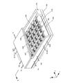
図1は、本実施の形態に係る画像表示装置に用いた表示パネルの斜視図であり、内部構造を示すためにパネルの一部を切り欠いて示している。図中、1005はリアプレート、1006は側壁、1007はフェースプレートであり、1005〜1007により表示パネルの内部を真空に維持するための気密容器を形成している。
【0027】
リアプレート1005には、基板1001が固定されているが、該基板上には画像形成素子としてのSCE1002がN×M個形成されている。行配線(走査配線)1003,列配線(変調配線)1004及びSCEは図2のように接続されている。
【0028】
また、フェースプレート1007の下面には、赤、青、緑の3原色の蛍光体1008が各画素に対応して形成されている。
【0029】
蛍光膜1008の下面にはメタルバック1009が形成されている。
【0030】
Hvは高圧端子でありメタルバック1009に電気的に接続されている。Hv端子に高電圧を印加することによりリアプレート1005とフェースプレート1007の間に高電圧が印加される。
【0031】
(SCEの特性)
SCEは、図3に示すような(放出電流Ie)対(素子印加電圧Vf)特性、及び(素子電流If)対(素子印加電圧Vf)特性を有する。なお、放出電流Ieは素子電流Ifに比べて著しく小さく、同一尺度で図示するのが困難であるため、2本のグラフは各々異なる尺度で図示した。
【0032】
SCEは、放出電流Ieに関して以下に述べる3つの特性を有している。
【0033】
第一に、ある電圧(これを閾値電圧Vthと呼ぶ)以上の電圧を素子に印加すると急激に放出電流Ieが増加するが、一方、閾値電圧Vth未満の電圧では放出電流Ieはほとんど検出されない。
【0034】
第二に、放出電流Ieは素子に印加する電圧Vfに依存して変化するため、電圧Vfを可変することにより、放出電流Ieの大きさを制御できる。
【0035】
第三に、高速な応答性を有しているため、電圧Vfの印加時間により放出電流Ieの放出時間を制御できる。
【0036】
図1に示した表示パネルを用いた画像表示装置において、第一の特性を利用すれば、表示画面を順次走査して表示を行うことが可能である。すなわち、駆動中の素子には所望の発光輝度に応じて閾値電圧Vth以上の電圧を適宜印加し、非選択状態の素子には閾値電圧Vth未満の電圧を印加する。駆動する素子を順次切り替えることにより、表示画面を順次走査して表示を行うことが可能である。
【0037】
また、第二の特性を利用することにより、素子に印加する電圧Vfにより、蛍光体の発光輝度を制御することができ、画像表示を行うことが可能である。
【0038】
また、第三の特性を利用することにより、素子に電圧Vfを印加する時間により、蛍光体の発光時間を制御することができ、画像の表示を行うことができる。
【0039】
本発明の画像表示装置では上記第三の特性を用いて変調を行った。
【0040】
(表示パネルの駆動方法)
図4は、本発明の表示パネルを駆動した際に走査配線及び変調配線の電圧供給端子に印加した電圧の一例である。
【0041】
ここで、水平走査期間Iは、i行目のピクセルを発光させる期間とする。
【0042】
i行目のピクセルを発光させるためには、i行目の走査配線を選択状態とし、その電圧供給端子Dxiに選択電位Vsを印加する。また、それ以外の走査配線の電圧供給端子Dxk(k=1,2,...N、但しk≠i)は非選択状態とし、非選択電位Vnsを印加する。
【0043】
本実施の形態では、選択電位Vsを図3に記載の電圧VSELの半分の−0.5VSELに設定し、非選択電位VnsはGND電位とした。
【0044】
また変調配線の電圧供給端子には、電圧振幅Vpwmのパルス幅変調信号を供給した。j番目の変調配線に供給するパルス幅変調信号のパルス幅は、従来、補正を行わない場合は、表示する画像の第i行第j列のピクセルの画像データの大きさに応じて決定し、すべての変調配線に各々のピクセルの画像データの大きさに応じたパルス幅変調信号を供給していた。
【0045】
なお、本発明においては、後述するように、電圧降下の影響による、輝度の低下を補正するために、j番目の変調配線に供給するパルス幅変調信号のパルス幅は、表示する画像の第i行第j列のピクセルの画像データの大きさと、その補正量に応じて決定し、すべての変調配線にパルス幅変調信号を供給する。
【0046】
本実施の形態では、電圧Vpwmの電圧は+0.5VSELに設定した。
【0047】
(走査配線での電圧降下について)
上述したように、本発明の画像表示装置の抱える根本的な課題は、表示パネルの走査配線における電圧降下によって、走査配線上の電位が上昇することにより、SCEに印加される電圧が減少するため、SCEからの放出電流が低下してしまうことである。以下、この電圧降下の機構について説明する。
【0048】
SCEの設計仕様や製法によっても異なるが、SCEの1素子分の素子電流は電圧VSELを印加した場合に数100μA程度である。
【0049】
このため、ある水平走査期間において選択された走査線上の1ピクセルのみを発光させ、それ以外のピクセルは発光させない場合には、変調配線から選択行の走査配線に流入する素子電流は1ピクセル分の電流(すなわち上述の数100μA)だけであるため、電圧降下はほとんど生じることはなく、発光輝度が低下することはない。
【0050】
しかし、ある水平走査期間において、選択された行の全ピクセルを発光させる場合には、全変調配線から選択状態としている走査配線に対し、全ピクセル分の電流が流入するため、電流の総和は数100mA〜数Aとなり、走査配線の配線抵抗によって走査配線上に電圧降下が発生していた。
【0051】
走査配線上に電圧降下が発生すれば、SCEの両端に印加される電圧が低下する。このためSCEから発光される放出電流が低下してしまい、結果として発光輝度が低下していた。
【0052】
また、さらに複雑なことに、電圧降下の大きさはパルス幅変調によって変調を行うことにより1水平走査期間の中でも変化する性質を持っている。
【0053】
各列に供給するパルス幅変調信号が、図4に示したように入力されるデータに対し、そのデータの大きさに依存したパルス幅の、立ち上がりが同期したパルス幅変調信号を出力する場合を考えてみる。このような場合、入力画像データにもよるが一般的には、1水平走査期間内では、パルスの立ち上がり直後ほど点灯しているピクセルの数が多く、その後輝度の低い箇所から順に消灯していくため、点灯するピクセルの数は一水平走査期間の中では、時間を追って減少する。
【0054】
したがって、走査配線上に発生する電圧降下の大きさも、1水平走査期間の初めほど大きく次第に減少していく傾向がある。
【0055】
パルス幅変調信号は変調の1階調に相当する時間ごとに出力が変化するため、電圧降下の時間的な変化もパルス幅変調信号の1階調に相当する時間毎に変化する。
【0056】
以上、走査配線における電圧降下について説明した。
【0057】
(電圧降下の計算方法)
次に、電圧降下の影響に対する補正の方法について詳述する。
【0058】
電圧降下の影響を低減するための補正量を求めるには、まずその第一段階として、電圧降下の大きさとその時間変化をリアルタイムに予測するハードウエアが必要とされるが、本発明のような画像表示装置の表示パネルとしては、数千本もの変調配線を備えることが一般的であり、変調配線のすべてと走査配線との交点の電圧降下を計算することは非常に困難であるとともに、それをリアルタイムに計算するハードウエアを作製することは現実的ではない。
【0059】
従って、同一行に位置に関してブロック化するとともに、画像データの大きさ方向へもブロック化することにより、電圧降下量を算出する。
【0060】
このようなブロック化は電圧降下における以下のような特徴に基づくものである。
【0061】
i)一水平走査期間のある時点においては、走査配線上に発生する電圧降下は走査配線上で空間的に連続的な量であり非常に滑らかなカーブである。
【0062】
ii)電圧降下の大きさは表示画像によっても異なるが、パルス幅変調の1階調に相当する時間毎に変化し、概略的にはパルスの立ち上がり部分ほど大きく、時間的には次第に小さくなるか、もしくはその大きさを維持するかのどちらかである。
【0063】
すなわち、図4のような駆動方法では1水平走査期間内で電圧降下の大きさが増加することはない。
【0064】
具体的には以下で説明する縮退モデルによる電圧降下の計算を複数の時刻に対して計算することによって、電圧降下の時間変化を概略的に予測した。
【0065】
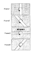
(縮退モデルによる電圧降下の計算)
図5(a)は、縮退を行う際のブロック及びノードを説明するための図である。
【0066】
図5では図を簡略化するため、選択された走査配線と各変調配線及びその交差部に接続されるSCEのみを記載した。
【0067】
いま、一水平走査期間の中のある時刻であって、選択された走査配線上の各ピクセルの点灯状態(すなわち変調手段の出力が”H”であるか、”L”であるか)が分かっているものとする。
【0068】
この点灯状態において、各変調配線から選択された走査配線へ流れ込む素子電流をIfi(i=1,2,...N,iは列番号)と定義する。
【0069】
また、図5に示すように、n本の変調配線と選択された走査配線のそれと交差する部分及び、その交点に配置されるSCEを1つのグループとしてブロックを定義する。本実施の形態では、ブロック分けを行うことで4つのブロックに分割した。
【0070】
また、各々のブロックの境界位置においてノードという位置を設定した。ノードとは、縮退モデルにおいて走査配線上に発生する電圧降下量を離散的に計算するための水平位置(基準点)である。
【0071】
本実施の形態ではブロックの境界位置に、ノード0〜ノード4の5つのノードを設定した。
【0072】
図5(b)は縮退モデルを説明するための図である。
【0073】
縮退モデルでは図5(a)の1ブロックに含まれるn本の変調配線を1本に縮退化し、縮退化された1本の変調配線が、走査配線のブロックの中央に位置するように接続した。
【0074】
また、縮退化された各々のブロックの変調配線には電流源が接続されており、各電流源から各々のブロック内の電流の総和IF0〜IF3が流れ込むものとした。
【0075】
すなわち、IFj(j=0,1,…3)は、
【数1】

【0076】
また、走査配線の両端の電位が図5(a)の例ではVsであるのに対し、図5(b)ではGND電位としているのは、縮退モデルでは、変調配線から選択した走査配線に流れ込む電流を上記電流源によりモデリングしたことにより、走査配線上の各部の電圧降下量は、その給電部を基準(GND)電位として各部の電圧(電位差)を算出することにより計算できるためである(つまり、電圧降下を算出する上での基準電位として規定した。)。
【0077】
また、SCEを省略しているのは、選択された走査配線から見た場合に、列配線から同等の電流が流れ込めば、SCEの有無によらず、発生する電圧降下自体は変わらないためである。従って、ここでは、各ブロックの電流源から流れ込む電流値を各ブロック内の素子電流の総和の電流値(式1)に設定することでSCEを省略した。
【0078】
また、各ブロックの走査配線の配線抵抗は一区間の走査配線の配線抵抗rのn倍とした(ここで一区間とは走査配線の、ある列配線との交差部とその隣の列配線との交差部との間のことを指している。また本実施の形態では、一区間の走査配線の配線抵抗は均一であるものとした。)。
【0079】
このような縮退モデルにおいて、走査配線上の各ノードにおいて発生する電圧降下量DV0〜DV4は以下のような積和形式の式により、簡単に計算することができる。
【0080】
【数2】
【0081】
すなわち、
【数3】
【0082】
ただし、aijは縮退モデルにおいてj番目のブロックだけに単位電流を注入したときに、i番目のノードに発生する電圧である(以下、これをaijと定義する。)。
【0083】
上記のaijはキルヒホフの法則により導出され、一度計算しておけば、テーブルとして記憶しておけばよい。
【0084】
さらに、式1で定めた各ブロックの総和電流IF0〜IF3に対し、
【数4】
【0085】
ただし、上式においてCountiは選択された走査線上のi番目のピクセルが点灯状態である場合には1をとり、消灯状態である場合には0をとる変数である。
【0086】
IFSはSCE1素子の両端に電圧VSELを印加したときに流れる素子電流IFに対し、0〜1の間の値をとる係数αをかけた量である。
【0087】
すなわち、
【数5】
【0088】
式2は、選択された走査配線に対し各ブロックの列配線から該ブロック内の点灯数に比例した素子電流が流れ込むものとしている。この際1素子の素子電流IFに係数αをかけたものを1素子の素子電流IFSとしたのは以下の理由による。
【0089】
本来、電圧降下量を計算するためには、電圧降下による走査配線の電圧上昇とそれによる素子電流の減少量とを繰り返し計算することが必要であるが、この収束計算をハードウエアで計算するのは現実的でない。
【0090】
そこで、本発明においては、IFの収束値として近似的にαIFを用いる。
【0091】
具体的には、電圧降下量が最大となるとき(全白のとき)のIFの低下率(=α1)と、電圧降下量が(最小=0)となるときのIFの低下率(=α2)を予め見積もっておいて、α1とα2の平均値または0.8×α1として求められる。
【0092】
図5(c)は、ある点灯状態において、縮退モデルにより各ノードの電圧降下量DV0〜DV4を計算した結果の一例である。
【0093】
電圧降下は非常に滑らかなカーブとなるため、ノードとノードの間の電圧降下は近似的には図5(c)の点線に示したような値をとると想定される。
【0094】
このように、本縮退モデルを用いれば、入力された画像データに対し所望の時点でのノードの位置での電圧降下を計算することが可能である。
【0095】
以上、ある点灯状態における電圧降下量を縮退モデルを用いて簡単に計算した。
【0096】
選択された走査配線上に発生する電圧降下は一水平走査期間内で時間的に変化するが、これについては前述したように一水平走査期間中のいくつかの時刻に対して、その時の点灯状態を求め、その点灯状態に対し縮退モデルを用いて電圧降下を計算することにより予測した。
【0097】
なお、一水平走査期間のある時点での各ブロック内の点灯数は各ブロックの画像データを参照すれば簡単に求めることができる。
【0098】
いま、1つの例としてパルス幅変調回路への入力データのビット数が8ビットであるものとし、パルス幅変調回路は入力データの大きさに応じたパルス幅を出力する。
【0099】
すなわち入力データが0のときは、出力は”L”となり、入力データが255のとき一水平走査期間の間は”H”を出力し、入力データが128のときには一水平走査期間のうち初めの半分の期間は”H”を出力し、後の半分の期間は”L”を出力するものとする。
【0100】
このような場合、パルス幅変調信号の開始時刻(本例の変調信号の例では立ち上がりの時刻)の点灯数は、パルス幅変調回路への入力データが0よりも大きいものの数をカウントすれば簡単に検出できる。
【0101】
同様に一水平走査期間の中央の時刻の点灯数は、パルス幅変調回路への入力データが128よりも大きいものの数をカウントすれば簡単に検出できる。
【0102】
このように画像データをある閾値に対してコンパレートし、コンパレータの出力が真である数をカウントすれば、任意の時間における点灯数が簡単に計算することができる。
【0103】
ここで以降の説明を簡単化するため、タイムスロットという時間量を定義する。
【0104】
すなわち、タイムスロットとは、一水平走査期間のなかのパルス幅変調信号の立ち上がりからの時間を表しており、タイムスロット=0とは、パルス幅変調信号の開始時刻直後の時刻を表すものと定義する。
【0105】
タイムスロット=64とは、パルス幅変調信号の開始時刻から、64階調分の時間が経過した時刻を表すものと定義する。
【0106】
同様にタイムスロット=128とは、パルス幅変調信号の開始時刻から、128階調分の時間が経過した時刻を表すものと定義する。
【0107】
なお、本例ではパルス幅変調は立ち上がり時刻を基準として、そこからのパルス幅を変調した例を示したが、同様に、パルスの立ち下がり時刻を基準として、パルス幅を変調する場合でも、時間軸の進む方向とタイムスロットの進む方向が逆となるが、同様に適用することができることはいうまでもない。
【0108】
(電圧降下量から補正データの計算)
上述したように、縮退モデルを用いて繰り返し計算を行うことで一水平走査期間中の電圧降下の時間変化を近似的かつ離散的に計算することができた。
【0109】
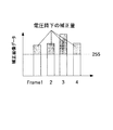
図6は、ある画像データに対して、電圧降下を繰り返し計算し、走査配線での電圧降下の時間変化を計算した例である(ここに示されている電圧降下及びその時間変化は、ある画像データに対する一例であって、別の画像データに対する電圧降下は、また別の変化をすることは当然である。)。
【0110】
図6ではタイムスロット=0,64,128,192の4つの時点に対して、各々縮退モデルを適用して計算を行うことに、それぞれの時刻の電圧降下を離散的に計算した。
【0111】
図6では各ノードにおける電圧降下量を点線で結んでいるが、点線は図を見やすくするために記載したものであって、本縮退モデルにより計算された電圧降下は□、○、●、△で示した各ノードの位置において離散的に計算した。
【0112】
本発明者らは、電圧降下の大きさとその時間変化を計算可能となった次の段階として、電圧降下量から画像データを補正する補正データを算出する方法について検討を行った。
【0113】
図7は、選択した走査配線上に図6に示した電圧降下が発生した際に、点灯状態にあるSCEから放出される放出電流を見積もったグラフである。
【0114】
縦軸は電圧降下がないときに放出される放出電流の大きさを100%として、各時間、各位置の放出電流の量を百分率で表しており、横軸は水平位置を表している。
【0115】
図7に示すように、ノード2の水平位置(基準点)において、
タイムスロット=0の時の放出電流をIe0,
タイムスロット=64の時の放出電流をIe1,
タイムスロット=128の時の放出電流をIe2,
タイムスロットが192の時の放出電流をIe3
とする。
【0116】
図7は、図6の電圧降下量と図3の”駆動電圧対放出電流”のグラフから計算した。具体的には電圧VSELから電圧降下量を引いた電圧が印加された際の放出電流の値を機械的にプロットしたものである。
【0117】
したがって、図7はあくまで点灯状態にあるSCEから放出される電流を意味しており、消灯状態にあるSCEが電流を放出することはない。
【0118】
以下に、電圧降下量から画像データを補正する補正データを算出する方法として、以下に説明を行う。
【0119】
(補正データ算出方法)
図8(a),(b),(c)は図7の放出電流の時間変化から、電圧降下量の補正データを計算する方法を説明するための図である。図8は大きさが64の画像データに対する補正データを算出した例である。
【0120】
輝度の発光量は、放出電流パルスによる放出電流を時間的に積分した、放出電荷量に他ならない。したがって以降では、電圧降下による輝度の変動を考えるのにあたって、放出電荷量をもとに説明を行う。
【0121】
いま、電圧降下の影響がない場合の放出電流をIEとし、パルス幅変調の1階調に相当する時間をΔtとするならば、画像データが64のときの、放出電流パルスによって放出されるべき放出電荷量Q0は放出電流パルスの振幅IEにパルス幅(64×Δt)をかけて、
【数6】
【0122】
しかし、実際には、走査配線上の電圧降下によって放出電流が低下する現象が発生する。
【0123】
電圧降下の影響を考慮した放出電流パルスによる放出電荷量は、近似的には次のように計算できる。すなわち、ノード2のタイムスロット=0,64の放出電流をそれぞれIe0,Ie1とし、0〜64の間の放出電流はIe0とIe1の間を直線的に変化するものと近似すれば、この間の放出電荷量Q1は図8(b)の台形の面積となる。
【0124】
すなわち、
【数7】
【0125】
次に、図8(c)に示すように、電圧降下による放出電流の低下分を補正するために、パルス幅をDC1だけ伸ばしたとき、電圧降下の影響を除去できたとする。
【0126】
また、電圧降下の補正を行い、パルス幅を伸ばした場合には、各タイムスロットにおける放出電流量は変化すると考えられるが、ここでは簡単化のため、図8(c)のように、タイムスロット=0では、放出電流がIe0、タイムスロット=(64+DC1)における放出電流がIe1になるものとする。
【0127】
また、タイムスロット0とタイムスロット(64+DC1)の間の放出電流は、2点の放出電流を直線で結んだ線上の値をとるものと近似する。
【0128】
すると、補正後の放出電流パルスによる放出電荷量Q2は、
【数8】
【0129】
これが前述のQ0と等しいとすれば、
【数9】
【0130】
これをDC1について解けば、
【数10】
【0131】
このようにして、画像データが64の場合の補正データを算出した。
【0132】
すなわち、ノード2の位置の大きさが64の画像データに対しては式8に記載のように、CData=DC1だけ補正量CDataを加算すればよい。
【0133】
同様に、大きさが192の画像データに対しては、図9のように、3つの期間の各々に対して補正量を求めることができる。
【0134】
また、パルス幅が0の時には、当然ながら放出電流に対する電圧降下の影響はないため、補正データは0とし画像データに加算する補正データCDataも0とした。
【0135】
なお、このように0,64,128,192というように、とびとびの画像データに対して補正データを計算しているのは、計算量を減らすことを狙ったものである。
【0136】
本方法により求めた、ある入力データに対する離散的補正データた例を図10(a)に示す。
【0137】
同図において横軸は水平表示位置に対応しており、各ノードの位置が記載されている。また、縦軸は補正データの大きさである。
【0138】
離散補正データは図の□、○、●、△で示したノードの位置と画像データDataの大きさ(画像データ基準値=0,64,128,192)に対して計算されているものである。
【0139】
(離散補正データの補間方法)
離散的に算出された補正データは、各ノードの位置に対する離散的なものであって、任意の水平位置(列配線番号)における補正データを与えるものではない。またそれと同時に、各ノード位置においていくつかの予め定められた画像データの基準値の大きさをもつ画像データに対する補正データであって実際の画像データの大きさに応じた補正データを与えるものではない。
【0140】
そこで、本発明者らは、各列配線における入力画像データの大きさに適合した補正データを、離散的に算出した補正データを補間することにより算出した。
【0141】
図10(b)はノードnとノードn+1の間に位置するxにおける、画像データDataに相当する補正データを算出する方法を示した図である。
【0142】
なお前提として、補正データはすでにノードn及びノードn+1の位置Xn及びXn+1において離散的に計算されているものとする。
【0143】
また、入力画像データであるDataは画像データ基準値のDkとDk+1の間の値をとるものとする。
【0144】
いま、ノードnのk番目の画像データの基準値に対する離散補正データをCData[k][n]と表記するならば、位置xにおけるパルス幅Dkの補正データCAは、CData[k][n]とCData[k][n+1]の値を用いて、直線近似により、以下のように計算できる。
【0145】
すなわち、
【数11】
【0146】
ただし、Xn、Xn+1はそれぞれノードn、(n+1)の水平表示位置であって、前述したブロックを決定するときに定められる定数である。
【0147】
また、位置xにおける画像データDk+1の補正データCBは以下のように計算できる。
【0148】
すなわち
【数12】
【0149】
CAとCBの補正データを直線近似することにより、位置xにおける画像データDataに対する補正データCDは、以下のように計算できる。
【0150】
すなわち、
【数13】
【0151】
以上のように、離散補正データから実際の位置や画像データの大きさに適合した補正データを算出するためには、式9〜式11に記載した方法により簡単に計算できる。
【0152】
このようにして算出した補正データを画像データに加算して画像データを補正し、補正後の画像データ(補正画像データと呼ぶ)に応じてパルス幅変調を行えば、従来からの課題であった表示画像における、電圧降下による影響を低減することができ、画質を向上させることができる。
【0153】
また、予てからの課題であった補正のためのハードウエアも、これまで説明してきた縮退化などの近似を導入することにより、計算量を低減化することができるため非常に小規模なハードウエアで構成することができるという優れたメリットがあった。
【0154】
(システム全体と各部分の機能説明)
次に、補正データ算出手段を内蔵した画像表示装置のハードウエアについて説明する。
【0155】
図11はその回路構成の概略を示すブロック図である。図において1は図1の表示パネル、Dx1〜DxM及びDx1’〜DxM’は表示パネル1の走査配線の電圧供給端子、Dy1〜DyNは表示パネル1の変調配線の電圧供給端子、Hvはフェースプレートとリアプレートの間に加速電圧を印加するための高圧供給端子、Vaは高圧電源、2は走査回路、3は同期信号分離回路、4はタイミング発生回路、7は同期分離回路3によりYPbPr信号をRGBに変換するためのRGB変換回路、23はテレビジョンの映像信号とコンピュータの映像信号を切り替えるためのセレクタ、17は逆γ処理部、5は画像データ1ライン分のシフトレジスタ、6は画像データ1ライン分のラッチ回路、8は表示パネルの変調配線に変調信号を出力するパルス幅変調手段、12は加算器、14は補正データ算出手段、20は最大値検出手段、21はゲイン算出手段である。
【0156】
また、図11においてR、G、BはRGBパラレルの入力映像データ、Ra,Ga,Baは後述する逆γ変換処理を施したRGBパラレルの映像データ、Dataはデータ配列変換部9によりパラレル・シリアル変換された画像データ、CDは補正データ算出手段14により算出された補正データ、Doutは加算器により画像データに補正データを加算することにより、補正された画像データ(補正画像データ)である。
【0157】
(同期分離回路、セレクタ)
本実施の形態の画像表示装置は、NTSCや、PAL、SECAM、HDTVなどのテレビジョン信号や、コンピュータの出力であるVGAなどをともに表示することができる。
【0158】
HDTV方式の映像信号は、まず同期分離回路3により同期信号Vsync,Hsyncを分離し、タイミング発生回路4に供給する。同期分離された映像信号は、RGB変換手段に供給される。RGB変換手段の内部には、YPbPrからRGBへの変換回路の他に、不図示のローパスフィルタやA/D変換器などが設けられており、YPbPrをディジタルRGB信号へと変換し、セレクタ23へと供給されている。
【0159】
VGAなどのコンピュータの出力する映像信号は、不図示のA/D変換器によりA/D変換され、セレクタ23へと供給される。
【0160】
セレクタ23はユーザーが表示したい映像信号がいずれであるかに基づいて、テレビジョン信号と、コンピュータ信号を適宜切り替えて出力する。
【0161】
(タイミング発生回路)
タイミング発生回路4は、PLL回路を内蔵しており、様々な映像フォーマットに対応したタイミング信号を発生し、各部の動作タイミング信号を発生する回路である。
【0162】
タイミング発生回路4が発生するタイミング信号としては、シフトレジスタ5の動作タイミングを制御するTsft、シフトレジスタ5からラッチ回路6へデータをラッチするための制御信号Dataload、変調手段8のパルス幅変調開始信号Pwmstart,パルス幅変調のためのクロックPwmclk、走査回路2の動作を制御するTscanなどがある。
【0163】
(走査回路)
図12に示すように、走査回路2及び2’は、表示パネルを一水平走査期間に1行ずつ順次走査するために、接続端子Dx1〜DxMに対して選択電位Vsまたは非選択電位Vnsを出力する回路である。
【0164】
走査回路2及び2’はタイミング発生回路4からのタイミング信号Tscanに同期して、一水平期間ごとに選択している走査配線を順次切り替え、走査を行う回路である。
【0165】
なお、Tscanは垂直同期信号及び水平同期信号などから作られるタイミング信号群である。
【0166】
走査回路2及び2’は、図12に示すようにそれぞれM個のスイッチとシフトレジスタなどから構成される。これらのスイッチはトランジスタやFETにより構成するのが好ましい。
【0167】
なお、走査配線での電圧降下を低減するためには、走査回路は図11に示したように、表示パネル1の走査配線の両端に接続され、両端からドライブされることが好ましい。
【0168】
一方、本発明の実施の形態では、走査回路が走査配線の両端に接続されていない場合でも有効であり、パラメータを変更するだけで適用できる。
【0169】
(逆γ処理部)
CRTは入力に対しほぼ2.2乗の発光特性(以降逆γ特性とよぶ)を備えている。
【0170】
入力映像信号はCRTのこのような特性が考慮されており、CRTに表示した際にリニアな発光特性となるように一般に0.45乗のγ特性にしたがって変換される。
【0171】
一方、本発明の実施の形態に係る画像表示装置の表示パネルは駆動電圧の印加時間により変調を施す場合、印加時間に対しほぼリニアな発光特性を有しているため、入力映像信号を逆γ特性に基づいて変換(以降逆γ変換とよぶ)する必要がある。
【0172】
図11に記載した逆γ処理部17は、入力映像信号を逆γ変換するための回路である。
【0173】
本実施の形態の逆γ処理部17は、上記逆γ変換処理をメモリによって構成した。
【0174】
逆γ処理部17は、映像信号R,G,Bのビット数を8ビットとし、逆γ処理部17の出力である映像信号Ra,Ga,Baのビット数を同じく8ビットとして、アドレス8ビット、データ8ビットのメモリを各色ごと用いることにより構成した(図13)。
【0175】
(データ配列変換部)
データ配列変換部9は、RGBパラレルな映像信号であるRa,Ga,Baを表示パネルの画素配列に合わせてパラレル・シリアル変換する回路である。データ配列変換部9の構成は、図14に示したようにRGB各色ごとのFIFO(FirstInFirstOut)メモリ2021R,2021G、2021Bとセレクタ2022から構成される。
【0176】
図14では図示していないが、FIFOメモリは水平画素数ワードのメモリを奇数ライン用と偶数ライン用の2本備えている。奇数行目の映像データが入力された際には、奇数ライン用のFIFOにデータが書き込まれる一方、偶数ライン用のFIFOメモリから一つ前の水平走査期間に蓄積された画像データが読み出される。偶数行目の映像データが入力された際には偶数ライン用のFIFOにデータが書き込まれる一方、奇数ライン用FIFOメモリから一つ前の水平期間に蓄積された画像データが読み出される。
【0177】
FIFOメモリから読み出されたデータは、セレクタにより表示パネルの画素配列にしたがって、パラレル・シリアル変換され、RGBのシリアル画像データSDataとして出力される。詳細については記載しないが、タイミング発生回路4からのタイミング制御信号に基づいて動作する。
【0178】
(遅延回路19)
データ配列変換部9により並び替えが行われた画像データSDataは補正データ算出手段14と遅延回路19に入力される。後述する補正データ算出手段14の補正データ補間部はタイミング制御回路からの水平位置情報xと画像データSDataの値を参照して、それらにあった補正データCDを算出する。
【0179】
遅延回路19は、補正データ算出(前述の補正データの補間処理)にかかる時間を吸収するために設けられており、加算器12で画像データDataに補正データCDが加算される際に、画像データDataにそれに対応した補正データCDが正しく加算されるよう遅延を行う手段である。同手段はフリップフロップを用いることにより構成できる。
【0180】
(加算器12)
加算器12は、補正データ算出手段14からの補正データCDと画像データDataを加算する手段である。加算を行うことにより画像データDataは補正が施され、補正画像データDoutとして最大値検出回路20及び乗算器へ転送される。
【0181】
なお加算器12の出力である補正画像データDoutのビット数は画像データに補正データを加算した際にオーバーフローが起きないように決定することが好ましい。
【0182】
より具体的には、画像データDataが8ビットのデータ幅であって、最大値が255、補正データCDは7ビットのデータ幅を持っていて、最大値が120であったとする。
【0183】
このとき加算結果の最大値は、255+120=375になった。
【0184】
これに対して加算器12の出力である補正画像データDoutは、オーバーフローが起きないように、出力ビット幅として9ビット出力であることが好ましい。
【0185】
(オーバーフロー処理(振幅調整手段))
本発明では、算出した補正データCDを画像データDataに加算した補正画像データDoutによって補正を実現することについてはすでに述べたとおりである。
【0186】
いま、変調手段8のビット数が8ビットであって、加算器12の出力である補正画像データDoutのビット数が9ビットであるものとする。
【0187】
すると、補正画像データDoutを変調手段8の入力にそのまま接続してしまうと、オーバーフローが起きることになる。
【0188】
すなわち8ビット以上のデータは8ビット分の変調手段では折り返して変調されてしまうため、画質が著しく低下することになる。
【0189】
そこで変調手段8に入力される前に、補正画像データの振幅を調整する必要がある。
【0190】
変調手段8の入力ビット数を多くすれば、変調手段8の入力でのオーバーフローを防止することはできるが、その一方で変調信号の出力するパルスのパルス幅をどこまでも伸ばせるというものではない。
【0191】
すなわち、本発明の画像表示装置は走査配線を順次選択して駆動を行うものであるため、変調手段8が出力するパルス幅は割り当てられた走査時間を超えてパルスを伸ばすことはできない。
【0192】
したがって、変調手段8の入力範囲の上限は、変調手段8のビット数によって定まる最大入力値か、もしくは変調を行うことができる最大パルス幅(すなわち1行の走査配線を選択する時間)に対応した入力データ値によって規定される。
【0193】
なお、本実施の形態では、変調手段8の入力範囲の上限は、変調手段8の入力データの最大値によって規定された場合の例として以降説明を行うものとする。
【0194】
オーバーフローを防止するための構成として、入力画像データが最大である全白パターン(画像データのビット数を8ビットとすると、(R,G,B)=(FFh,FFh,FFh))を入力した際の、補正画像データDoutの最大値を予め見積もり、それが変調手段8の入力範囲に収まるようなゲインを補正画像データDoutに乗算してもよい。以下、本方法を固定ゲイン法と呼ぶ。
【0195】
固定ゲイン法では、オーバーフローは発生しないが、平均輝度が低い画像については、より大きなゲインで表示ができるのにもかかわらず、小さなゲインが乗算されてしまうため、表示画像の輝度が暗くなることがある。
【0196】
これに対し、フレームごとの補正画像データDoutの最大値を検出し、この最大値が変調手段8の入力範囲に収まるようなゲインを算出し、ゲインと補正画像データDoutを乗算してオーバーフローを防止してもよい。以下、本方法を適応型ゲイン法とよぶ。
【0197】
適応型ゲイン法では、補正画像データDoutのフレームごとの最大値MAXを検出するための最大値検出手段20と、最大値から補正画像データDoutに乗算するためのゲインG1を算出するためのゲイン算出手段21、及び補正画像データDoutとゲインG1を乗算するための乗算器などが必要である。
【0198】
なお、適応型ゲイン法では、オーバーフローを防止するためのゲインを算出するのは、フレームを単位として算出することが好ましい。
【0199】
たとえば1水平ラインごとにゲインを算出してオーバーフローを防止することもできるが、その場合1水平ラインごとのゲインの違いにより、表示画像に違和感が発生するため好ましくない。
【0200】
以上、固定ゲイン法、及び適応型ゲイン法の概略について説明した。
【0201】
本発明者らは、いずれの方法でゲインを算出しても好適に補正画像データの振幅を調整できることを確認している。
【0202】
そこで本実施の形態では、適応型ゲイン法により振幅調整を行うこととした。
【0203】
以降、本実施の形態では適応型ゲイン法により補正画像データの振幅調整を行うための手段としての、回路構成について詳しく説明する。
【0204】
(最大値検出手段(最大値検出部))
本発明の最大値検出手段20は図11に示すように、各部と接続されている。
【0205】
最大値検出手段20は、1フレーム分の補正画像データDoutのなかで、最大となる値を検出する手段である。
【0206】
最大値検出手段20は、コンパレータとレジスタなどによって簡単に構成できる回路である。最大値検出手段20は、レジスタに記憶されている値と、順次転送されてくる補正画像データDoutの大きさを比較し、補正画像データDoutの方がレジスタの値よりも大きければ、レジスタの値をそのデータ値で更新する回路である。
【0207】
レジスタの値は、フレームの先頭で0にクリアすれば、フレームの終了時には、そのフレーム中の補正画像データの最大値がレジスタに格納される。
【0208】
このようにして検出された補正画像データDoutの最大値は、ゲイン算出手段21へと転送される。
【0209】
(ゲイン算出手段(ゲイン算出部))
ゲイン算出手段21は、適応型ゲイン法に基づいて補正画像データDoutが変調手段8の入力範囲に収まるように、振幅調整を行うためのゲインを算出する手段である。
【0210】
ゲインは、最大値検出手段20の検出した最大値をMAX、変調手段の入力範囲の最大値をINMAXとすると、
【数14】
【0211】
ゲイン算出手段21では、垂直帰線期間においてゲインを更新して1フレーム毎にゲインの値が変更される。
【0212】
なお、本発明の画像表示装置の構成では、1フレーム前の補正画像データの最大値を用いて、現在のフレームの補正画像データに乗算するゲインを算出する構成となっている。
【0213】
したがって厳密には、フレームごとの補正画像データの違いから、オーバーフローが起きることがある。
【0214】
このような課題に対し、補正画像データとゲインを乗算する乗算器の出力に対し後述するリミッタ手段を設け、乗算器の出力が変調手段の入力範囲に収まるように回路を設計したところ好ましかった。上記のオーバーフロー処理は、隣接するフレーム間の補正画像データ(画像データ)の相関を利用してオーバーフロー処理を行っていると考えることができる。
【0215】
なお、最大値検出回路と、乗算器の間にフレームメモリを設ければ、時間的な遅延のない構成でオーバーフローを防止することができる。
【0216】
また、本発明者らは、適応型ゲイン法のゲイン決定方法は、以下のような方法によってゲインを算出してもよいことを確認している。
【0217】
すなわち、現在のフレームの補正画像データに施すゲインとしては、現在のフレームよりも以前のフレームで検出された補正画像データの最大値をフレーム方向に平滑化(平均化)し、その平均値AMAXに対し、ゲインG1’は、
【数15】
【0218】
また、3番目の方法は、式12により各々のフレームごとのゲインG1を算出し、それを平均化して現在のゲインを算出してもよい。
【0219】
本発明者らは、これら3つの方法のうち、どの方法も好ましいことを確認しているが、その一方で第1の方法よりも、第2、第3の方法の方が、表示画像におけるフリッカが大きく減少されるという別の効果があり非常に好適である(これについては後で図15〜図17を用いて説明する。)。
【0220】
本発明者らは、第2の方法、第3の方法に対して、平均化するフレームの枚数について検討を行ったが、たとえば16フレーム〜64フレームを平均化したところフリッカの少ない、好ましい画像が得られた。
【0221】
なお、第2、第3の方法の場合においても、第1の方法と同様に(補正)画像データにフレーム間の相関があることにより、オーバーフローが発生する確率を減少させることができるが、完全にオーバーフローを防止することができない。
【0222】
このための対策としては、上述の方法で概略的にオーバーフローを防止するとともに、乗算器の出力にリミッタを設けて完全にオーバーフローを防止したところ、さらに好ましかった。
【0223】
図15は、第1の方法と、第2の方法を例に挙げて、フリッカについて説明するための図である。
【0224】
図15は、グレーの背景のなかで、白い棒が反時計周りに回転する動画像の例である。このような画像を表示する場合、棒が回転するのに合わせて、フレーム毎に補正データCDの大きさが変化する。
【0225】
図16は、このような動画像を補正した際の補正画像データを説明するための図である。図16では各々の補正画像データのうち、各々のフレームで最大となったものを抜き出してグラフ化したものである。
【0226】
なお、図16の白の部分は元々の画像データ、灰色の部分は補正を行うことによって伸長された部分に相当する。
【0227】
図15のような画像を表示した場合、連続するフレームの補正画像データの最大値が図16に示すように変動する。
【0228】
したがって、式12に示したようにフレームごとにゲインを設定すると、図17(a)に示すようにフレーム毎のゲインの変動が激しくなるため、結果として表示画像の輝度変動が激しくなり、フリッカ感が発生する。
【0229】
これに対し式13によってゲインを決定した場合は、ゲインが平均化されるため、図17(b)に示したように、ゲインの変動が小さくなり、輝度の変動が少なくなるためフリッカ感が減少するという優れた効果があった。
【0230】
なお、図17(b)では、白丸のグラフが式12によるゲイン、黒丸のグラフが式13による平均化されたゲインである。
【0231】
第3の方法についてはここでは詳しく考察しなかったが、第2の方法と同様にゲインの変動が小さくなるためフリッカが減少することを本発明者らは確認している。
【0232】
また、ゲイン算出手段21は、上述のような連続的なシーンの画面に対しては、ゲインを平均化するが、一方、画像のシーンが変わった際には、シーンが変わったあとのゲインに速やかに変化させることが好ましかった。
【0233】
これに対しゲイン算出手段21は、シーン切り替えしきい値Gthなる、予め設定された閾値を設けておき、式12によって計算した1つ前のフレームのゲインをGB、前のフレームの最大値検出手段20が検出した前記補正画像データの最大値から式12によって計算されるゲインをGN、GN−GBの差の絶対値をΔGとすると、
【数16】
【数17】
【0234】
とくにA,及びBの値としては、
A=1、B=1/16〜1/64
程度に設定したところ好ましかった。
【0235】
なお、シーンの切り替えの判定、及びゲインの算出方法はこれに限らず、後述の第8の実施の形態に示すような構成によって検出してもよい。
【0236】
(乗算器)
ゲイン算出手段21で算出されたゲインG1と加算器12の出力である補正画像データDoutは、図11の乗算器によって乗算され、振幅が調整された補正画像データDmultとしてリミッタ回路へ転送される。
【0237】
(リミッタ手段(制限手段))
以上のようにして、オーバーフローが起きないようにゲインを決定できれば問題ないが、上述したいくつかのゲイン決定方法によれば、必ずオーバーフローが起きないようにゲインを決定することは困難であるので、リミッタ(Limiter)を設けておくこともできる。
【0238】
リミッタは、予め設定されたリミット値を有し、リミッタに入力される出力データDmultとリミット値を比較し、出力データよりもリミット値が小さければ、リミット値を出力し、出力データよりもリミット値が大きければ、出力データを出力する(図11における信号名は補正画像データDlim)。
【0239】
リミッタ手段によって、変調手段8の入力範囲に完全に制限された補正画像データDlimは、シフトレジスタ、ラッチを介して変調手段8へと供給される。
【0240】
(シフトレジスタ、ラッチ回路)
リミッタ回路の出力である補正画像データDlimは、シフトレジスタ5により、シリアルなデータフォーマットから、各変調配線毎のパラレルな画像データID1〜IDNへとシリアル/パラレル変換されラッチ回路6へ出力される。ラッチ回路6では、1水平期間が開始される直前にタイミング信号Dataloadにより、シフトレジスタ5からのデータをラッチする。ラッチ回路6の出力は、パラレルな画像データD1〜DNとして変調手段8へと供給される。
【0241】
本実施の形態では画像データID1〜IDN、D1〜DNはそれぞれ8ビットの画像データとした。これらの動作タイミングはタイミング発生回路4(図11)からのタイミング制御信号TSFT及びDataloadに基づいて動作する。
【0242】
(変調手段の詳細)
ラッチ回路6の出力であるパラレル画像データD1〜DNは変調手段8へと供給される。
【0243】
変調手段8は、図18(a)に示したように、PWMカウンタと、各変調配線ごとにコンパレータとスイッチ(同図ではFET)を備えたパルス幅変調回路(PWM回路)である。
【0244】
画像データD1〜DNと変調手段の出力パルス幅の関係は、図18(b)のようなリニアな関係にある。
【0245】
図18(c)に変調手段の出力波形の例を3つ示す。
【0246】
図18(c)において、上側の波形は、変調手段への入力データが0の時の波形、中央の波形は、変調手段への入力データが128の時の波形、下側の波形は、変調手段への入力データが255の時の波形である。
【0247】
なお、本例では変調手段への入力データD1〜DNのビット数は8ビットとした。
【0248】
なお、前述の説明では、変調手段の入力データが255のときは、一水平走査期間に相当するパルス幅の変調信号が出力されると記載した箇所があるが、詳細には同図(c)のように非常に短い時間ではあるがパルスの立ち上がる前と、立ち下がった後にわずかではあるが駆動しない期間を設けタイミング的な余裕を持たせている。
【0249】
図19は、本発明の変調手段の動作を示すタイミングチャートである。
【0250】
図19において、Hsyncは水平同期信号、Dataloadはラッチ回路6へのロード信号、D1〜DNは前述の変調手段の列1〜Nへの入力信号、PwmstartはPWMカウンタの同期クリア信号、PwmclkはPWMカウンタのクロックである。また、XD1〜XDNは変調手段の第1〜第N列の出力を表している。
【0251】
図19にあるように1水平走査期間が始まると、ラッチ回路6は画像データをラッチするとともに変調手段8へデータを転送する。
【0252】
PWMカウンタは、同図に示したように、Pwmstart、Pwmclkに基づいてカウントを開始し、カウント値が255になるとカウンタをストップしカウント値255を保持する。
【0253】
各列毎に設けられているコンパレータは、PWMカウンタのカウント値と各列の画像データを比較し、PWMカウンタの値が画像データ以上のときHighを出力し、それ以外の期間はLowを出力する。
【0254】
コンパレータの出力は、各列のスイッチのゲートに接続されており、コンパレータの出力がLowの期間は同図の上側(Vpwm側)のスイッチがON、下側(GND側)のスイッチがOFFとなり、変調配線を電圧Vpwmに接続する。
【0255】
逆にコンパレータの出力がHighの期間は、同図の上側のスイッチがOFFし、下側のスイッチがONするとともに、変調配線の電圧をGND電位に接続する。
【0256】
各部が以上のように動作することで、変調手段が出力するパルス幅変調信号は、図19のD1、D2、DNに示したような、パルスの立ち上がりが同期した波形となる。
【0257】
(補正データ算出手段)
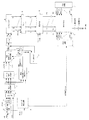
補正データ算出手段14は前述した補正データ算出方法により、電圧降下の補正データを算出する回路である。補正データ算出手段14は、図20に示すように離散補正データ算出部と補正データ補間部の2つのブロックから構成される。
【0258】
離散補正データ算出部では、入力された映像信号から電圧降下量を算出し、電圧降下量から補正データを離散的に計算する。離散補正データ算出部は、計算量やハードウエア量を減少させるために、前述の縮退モデルの概念を導入して、補正データを離散的に算出する。
【0259】
離散的に算出された補正データは補正データ補間部により補間され、画像データの大きさやその水平表示位置xに適合した補正データCDが算出される。
【0260】
(離散補正データ算出部)
図21は、本発明の離散的に補正データを算出するための離散補正データ算出部である。
【0261】
離散補正データ算出部は、以下に述べるように、画像データをブロックわけし、ブロックごとの統計量(点灯数)を算出するとともに、統計量から各ノードの位置における、電圧降下量の時間変化を計算する電圧降下量算出部としての機能と、各時間ごとの電圧降下量を発光輝度量に変換する機能、及び発光輝度量を時間方向に積分して、発光輝度総量を算出する機能、及びそれらから離散的な基準点における、画像データの基準値に対する補正データを算出する手段である。
【0262】
図21において100a〜100dは点灯数カウント手段、101a〜101dは各ブロックごとの、各時刻における点灯数を格納するレジスタ群、102はCPU、103は式2及び式3で記載したパラメータaijを記憶するためのテーブルメモリ、104は計算結果を一時記憶するためのテンポラリレジスタ、105はCPUのプログラムが格納されているプログラムメモリ、111は、電圧降下量を放出電流量に変換する変換データが記載されたテーブルメモリ、106は、前述した離散補正データの計算結果を格納するためのレジスタ群である。
【0263】
点灯数カウント手段100a〜100dは、図21(b)に記載したようなコンパレータと加算器などから構成されている。映像信号Ra,Ga,Baはそれぞれコンパレータ107a〜cに入力され、逐次Cvalの値と比較される。
【0264】
なお、Cvalは前述してきた画像データに対して設定した、画像データ基準値に相当する。
【0265】
コンパレータ107a〜cはCvalと画像データの比較を行い画像データの方が大きければHighを出力し小さければLowを出力する。
【0266】
コンパレータの出力は加算器108及び109により互いに足し算され、さらに加算器110によりブロックごとに加算を行い、ブロックごとの加算結果を各々のブロックごとの点灯数としてレジスタ群101a〜dへと格納する。
【0267】
点灯数カウント手段100a〜dにはコンパレータの比較値Cvalとしてそれぞれ0、64、128、192が入力されている。
【0268】
結果として、点灯数カウント手段100aは画像データのうち、0より大きい画像データの個数をカウントしそのブロックごとの総計をレジスタ101aに格納する。
【0269】
同様に、点灯数カウント手段100bは画像データのうち、64より大きい画像データの個数をカウントし、そのブロックごとの総計をレジスタ101bに格納する。
【0270】
同様に、点灯数カウント手段100cは画像データのうち、128より大きい画像データの個数をカウントし、そのブロックごとの総計をレジスタ101cに格納する。
【0271】
同様に、点灯数カウント手段100dは画像データのうち、192より大きい画像データの個数をカウントし、そのブロックごとの総計をレジスタ101dに格納する。
【0272】
ブロックごと、時間ごとの点灯数カウントされると、CPUはテーブルメモリ103に格納されたパラメータテーブルaijを随時読み出して、式2〜式4に従い、電圧降下量を計算し、計算結果をテンポラリレジスタ104に格納する。
【0273】
本実施の形態ではCPUに式2の計算を円滑に行うための積和演算機能を設けた。
【0274】
式2に挙げた演算を実現する手段としては、CPUで積和演算を行わないでもよく、例えば、その計算結果をメモリに入れておいてもよい。
【0275】
すなわち、各ブロックの点灯数を入力とし、考えられるすべての入力パターンに対し、各ノード位置の電圧降下量をメモリに記憶させておいてもかまわない。
【0276】
電圧降下量の計算が完了するとともに、CPUはテンポラリレジスタ104から、各時間、各ブロックごとの電圧降下量をよみだし、テーブルメモリ2(111)を参照して、電圧降下量を放出電流量に変換し、式5〜式8に従って、離散補正データを算出した。
【0277】
計算した離散補正データは、レジスタ群106に格納した。
【0278】
(補正データ補間部)
補正データ補間部は画像データの表示される位置(水平位置)及び、画像データの大きさに対応した補正データを算出するための手段である。同手段は離散的に算出された補正データを補間することにより、画像データの表示位置(水平位置)及び、画像データの大きさに応じた補正データを算出する。
【0279】
図22は補正データ補間部を説明するための図である。
【0280】
図22において、デコーダ123は、画像データの表示位置(水平位置)xから、補間に用いる離散補正データのノード番号n及びn+1を決定するためのデコーダであり、デコーダ124は、画像データの大きさから、式9〜式11のk及びk+1を決定するためのデコーダである。
【0281】
また、セレクタ125〜128は、離散補正データを選択して、直線近似手段120,121に供給するためのセレクタである。
【0282】
また、直線近似手段120〜122は、それぞれ式9〜式11の直線近似を行うための直線近似手段a〜cである。
【0283】
図23に直線近似手段aの構成例を示す。一般に直線近似手段は式9〜式11の演算子にあらわされるように、減算器、積算器、加算器、割り算器などによって構成可能である。
【0284】
しかし、望ましくは離散補正データを算出するノードとノードの間の列配線本数や、離散補正データを算出する画像データ基準値の間隔(すなわち電圧降下を算出する時間間隔)が2のべき乗になるように構成するとハードウエアを非常に簡単に構成できるというメリットがある。それらを2のべき乗に設定すれば、図23に示した割り算器において、Xn+1−Xnは2のべき乗の値となり、ビットシフトすればよい。
【0285】
Xn+1−Xnの値がいつも一定の値であって、2のべき乗で表される値であるならば、加算器の加算結果をべき乗の乗数分だけシフトして出力すればよく、あえて割り算器を作製する必要がない。
【0286】
また、これ以外の箇所でも離散補正データを算出するノードの間隔や、画像データの間隔を2のべき乗とすることにより、たとえばデコーダ123〜124を簡単に作製することが可能となるとともに、図23の減算器で行っている演算を簡単なビット演算に置き換えることができるなど、非常にメリットが多い。
【0287】
(各部の動作タイミング)
図24に各部の動作タイミングのタイミングチャートを示す。
【0288】
なお、図24においてHsyncは水平同期信号、DotCLKはタイミング発生回路の中のPLL回路により水平同期信号Hsyncから作成したクロック、R、G、Bは入力切り替え回路からのディジタル画像データ、Dataはデータ配列変換後の画像データ、Dlimはリミッタ手段の出力であって、電圧降下補正を施された補正画像データ、TSFTはシフトレジスタ5へ補正画像データDlimを転送するためのシフトクロック、Dataloadはラッチ回路6へデータをラッチするためのロードパルス、Pwmstartは前述のパルス幅変調の開始信号、変調信号XD1は変調配線1へ供給されるパルス幅変調信号の一例である。
【0289】
1水平期間の開始とともに、セレクタ23からディジタル画像データRGBが転送される。図24では水平走査期間Iにおいて、入力される画像データをR_I、G_I、B_Iで表すと、それらは、データ配列変換回路9では1水平期間の間、画像データを蓄えられ、水平走査期間I+1において、表示パネルの画素配置に合わせてディジタル画像データData_Iとして出力される。
【0290】
R_I、G_I、B_Iは、水平走査期間Iにおいて補正データ算出手段14に入力される。補正データ算出手段14では、前述した点灯数をカウントし、カウントの終了とともに、電圧降下量が算出される。
【0291】
電圧降下量が算出されるのにつづいて、離散補正データが算出され、算出結果がレジスタに格納される。
【0292】
走査期間I+1に移り、データ配列変換部から、1水平走査期間前の画像データData_Iが出力されるのに同期して、補正データ補間手段では離散補正データが補間され、補正データが算出される。補間された補正データは、加算器12に供給される。
【0293】
加算器12では、画像データDataと補正データCDを順次加算し、補正された補正画像データDlimをシフトレジスタ5へ転送する。シフトレジスタ5はTSFTにしたがって、一水平期間分の補正画像データDlimを記憶するとともにシリアル・パラレル変換を行い、パラレルな画像データID1〜IDNをラッチ回路6に出力する。ラッチ回路6はDataloadの立ち上がりにしたがってシフトレジスタ5からのパラレル画像データID1〜IDNをラッチし、ラッチされた画像データD1〜DNをパルス幅変調手段8へと転送する。
【0294】
パルス幅変調手段8は、ラッチされた画像データに応じたパルス幅のパルス幅変調信号を出力する。本実施の形態の画像表示装置では、結果として、変調手段が出力するパルス幅は、入力された画像データに対し、2水平走査期間分おくれて表示される。
【0295】
このような画像表示装置により画像の表示を行ったところ、従来からの課題であった走査配線における電圧降下量を補正することができ、それに起因する表示画像の劣化を改善することができ、非常に良好な画像を表示することができた。
【0296】
また、いくつかの近似を導入したことにより、電圧降下を補正するための、画像データの補正量を簡単に好適に計算することができ、非常に簡単なハードウエアでそれを実現することができるなど、非常に優れた効果があった。
【0297】
(第2の実施の形態)
第1の実施の形態では、補正画像データの最大値を検出し、該最大値が,変調手段の入力範囲の最大値に対応するように、ゲインを算出し、該ゲインと補正画像データを乗算し、オーバーフローを防止していた。
【0298】
これに対し、第2の実施の形態では、補正画像データの最大値を検出するのは同様であるが、該最大値が変調手段の入力範囲の最大値に対応するように、補正を施す前の画像データの大きさを制限することとした。
【0299】
すなわち、オーバーフローが起きないように、予め入力された画像データにゲインを乗算してその振幅範囲を小さくしておき、オーバーフローを防止する。
【0300】
以降、図25を用いて、本実施の形態のオーバーフロー処理について説明する。
【0301】
図25において22R,22G,22Bは乗算器、9はデータ配列変換部、5は画像データ1ライン分のシフトレジスタ、6は画像データ1ライン分のラッチ回路、8は表示パネルの変調配線に変調信号を出力するパルス幅変調手段、12は加算器、14は補正データ算出手段、20はフレーム内の補正画像データDoutの最大値を検出するための最大値検出回路(手段)、21はゲイン算出手段である。
【0302】
また、R、G、BはRGBパラレルの入力映像データ、Ra,Ga,Baは逆γ変換処理を施したRGBパラレルの映像データ、Rx,Gx,Bxは乗算器により、ゲインG2が乗算された画像データ、ゲインG2は、ゲイン算出部が算出したゲイン、Dataはデータ配列変換部9によりパラレル・シリアル変換された画像データ、CDは補正データ算出手段14により算出された補正データ、Doutは加算器12により画像データDataに補正データCDを加算することにより、補正された画像データ(補正画像データ)、DlimはリミッタによってDoutを変調手段の入力範囲の上限以下に制限した補正画像データである。
【0303】
(乗算器22R、22G、22B)
乗算器22R,22G,22Bは逆γ変換後の画像データRa,Ga,Baに対し、ゲインG2を乗算するための手段である。
【0304】
より詳しくは、乗算器はゲイン算出手段21が決定したゲインに従って画像データにゲインG2を乗算し、乗算後の画像データRx,Gx、Bxを出力する。
【0305】
ゲインG2は、ゲイン算出手段21が算出する値であって、後述する加算器12での画像データDataと補正データCDの加算結果である補正画像データDoutが、変調手段8の入力範囲に収まるように決定される値である。
【0306】
(最大値検出手段(最大値検出部))
次に、最大値検出手段20について説明を行う。
【0307】
本発明の最大値検出手段20は、図25に示すように、各部と接続されている。
【0308】
最大値検出手段20は、1フレーム分の補正画像データDoutのなかで、最大となる値を検出する手段であってその構成及び動作は第1の実施の形態と同じである。検出された補正画像データの最大値MAXは、ゲイン算出手段21へと転送される。
【0309】
(ゲイン算出手段(ゲイン算出部))
ゲイン算出手段21は、最大値検出手段20の検出値MAXを参照して、補正画像データDoutが変調手段の入力範囲に収まるようにゲインを算出する手段である。本実施の形態においても、ゲイン算出手段21は適応型ゲイン法に基づいて補正画像データの振幅を調整するためのゲインを算出する。
【0310】
一方、別のゲインを算出する方法として、本実施の形態(図25)の構成においてゲインは固定ゲイン法によって算出してもよい。
【0311】
ゲインの決定方法は、1フレーム内の補正画像データDoutの最大値をMAX、変調手段の入力範囲の最大値をINMAX、前のフレームに対してゲイン算出手段が算出したゲインG2をGBとすると、
【数18】
【0312】
このゲイン算出手段21では、垂直帰線期間においてゲインを更新して1フレーム毎にゲインの値が変更される。
【0313】
なお、本実施の形態の画像表示装置の構成では、1フレーム前の補正画像データの最大値を用いて、現在のフレームの補正画像データに乗算するゲインを算出する構成となっている(すなわち、フレーム間の補正画像データ(画像データ)の相関を利用して、オーバーフローを防止する構成になっている。)。
【0314】
したがって厳密には、フレームごとの補正画像データの違いから、オーバーフローが起きることある。
【0315】
このような課題に対し、補正画像データとゲインを乗算する乗算器の出力に対しリミッタ手段を設け、乗算器の出力が必ず変調手段の入力範囲に収まるように回路を設計したところ、さらに好ましかった。
【0316】
また、本発明者らは、第1の実施の形態と同様に、フリッカを防止するという別の効果を得るために、現在のフレームよりも以前のフレームで検出された補正画像データの最大値を平均し、その平均値AMAXに対し、
【数19】
【0317】
また、別の方法は、式14により各々のフレームごとのゲインG2を算出し、それを平均化して現在のゲインを算出してもよい。
【0318】
本発明者らは、これら3つの方法のうち、どの方法でもオーバーフローを防止する意味では好ましいことを確認しているが、第1の実施の形態で述べたようにフリッカが発生することを考慮すれば、平均化を行って算出することが好ましい。
【0319】
本発明者らは、式15のゲイン算出法において、補正画像データの最大値を平均化するフレームの枚数について検討を行ったが、現在のフレームから16〜64フレーム前までの補正画像データの最大値を平均化したところ、好ましかった。
【0320】
なお、本方法でも、より好ましくは図25に示したように、加算器の出力を制限するリミッタを設けて完全にオーバーフローを防止することが好ましいことはいうまでもない。
【0321】
また、第1の実施の形態と同様にシーンチェンジの検出を行って、ゲインの算出の方法を変更してもよい。
【0322】
(第3の実施の形態)
第1の実施の形態では、入力画像データに対し、離散的な画像データの基準値を設定するとともに、行配線上に基準点を設定し、該基準点における、画像データ基準値の大きさの画像データに対する補正データを算出していた。
【0323】
さらに離散的に算出された補正データを補間することにより、入力された画像データの水平表示位置と、その大きさに応じた補正データを算出し、加算器によって画像データと加算することにより、補正を実現していた。
【0324】
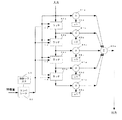
一方、図26の構成によっても同様な補正が行うことができる。以下に図26を用いて第3の実施の形態を説明する。
【0325】
図26において、図11との差異は、14の補正データ算出手段、加算器12を削除し、その代わりに離散補正画像データ算出部(手段)14a、補正画像データ補間回路(手段)14bを新たに設けた点である。
【0326】
下記に図26の画像表示装置の補正画像データを算出する流れを説明する。
【0327】
(1)離散的な水平位置と、画像データ基準値に対する、離散補正画像データCDA(すなわち前記離散補正データと画像データ基準値の和である補正の結果)を算出する(離散補正画像データ算出部)。
【0328】
(2)離散的に算出された補正画像データを補間し、入力された画像データDataの大きさと、その水平表示位置xに応じた補正画像データを算出する(補正画像データ補間回路)。
【0329】
(3)補間された補正画像データの最大値を検出し(最大値検出手段)、これが変調手段の入力範囲に収まるように、ゲインG1を算出する(ゲイン算出手段)。算出されたゲインG1と補正画像データDoutを乗算し(乗算器)、さらにリミッタで補正画像データの振幅を完全に制限して、シフトレジスタ、ラッチ、変調手段へと入力する。
【0330】
なお、(1)で述べた離散補正画像データCDAの算出方法は、これまでの離散補正データ算出の方法(式5〜式8)を変形すれば簡単に計算できる。
【0331】
すなわち、式5〜式8は画像データ基準値=0,64,128,192に対する離散補正データを算出するための式であったが、この離散補正データにそれぞれの画像データ基準値を加算した値を離散補正画像データCDAとすればよい。
【0332】
このような構成では、離散的に計算を行う段階で、画像データと補正データが加算された補正画像データを算出しているため、補間後に画像データと補正データの加算を行う必要はない。このため、図11の加算器12は不要となった。
【0333】
また、補正画像データ補間回路の構成は、第1の実施の形態で説明した図22の補正データ補間部と同じ構成で構成できる。
【0334】
以上、このような構成によっても、電圧降下の影響を好適に補正することができ、非常に好ましかった。
【0335】
なお本実施の形態では、補正画像データのオーバーフローを防止するための構成は、第1の実施の形態の構成を採用したが、特にこれに限定されることはなく、第2の実施の形態の構成を採用してもよいことはいうまでもない。
【0336】
(第4の実施の形態)
第3の実施の形態では入力画像データに対し、離散的な画像データの基準値を設定するとともに行配線上に基準点を設定し、該基準点における、画像データ基準値の大きさの画像データに対する補正画像データを算出していた。
【0337】
さらに離散的に算出された補正画像データを補間することにより、入力された画像データの水平表示位置と、その大きさに応じた補正画像データを算出していた。
【0338】
さらに算出された補正画像データDoutにゲインを乗算することによって、補正画像データDoutの振幅を調整し、変調手段の入力範囲に対応するように調整を行っていた。
【0339】
さらにゲインは、1フレーム前の補正画像データの最大値が、変調手段の入力範囲の最大値に対応するように、式14にしたがって算出していた。
【0340】
また、ゲインはフリッカ感を防止するという別の目的から、式15にしたがって算出していた。
【0341】
一方、図27の構成によっても同様な効果を得ることができる。以下に図27を用いて第4の実施の形態を説明する。
【0342】
図27において、図26との差異は、ゲイン算出手段21が算出したゲインの値を離散補正画像データCDAに乗算している点である。
【0343】
ゲインが乗算されることによって、離散補正画像データCDAはその振幅が調整され、CDLとして補正画像データ補間回路14bに出力される。
【0344】
補正画像データ補間回路14bは、振幅が調整された離散補正画像データであるCDLに基づいて、入力された画像データDataの大きさと、その水平表示位置xに応じた補正画像データDoutを算出する。
【0345】
なお、この際に補正画像データ補間回路14bの出力Doutは、すでに変調手段の入力範囲に収まるように振幅調整が行われていることになる。
【0346】
ただし、厳密には離散補正画像データに乗算する際のゲインG3は、
【数20】
【数21】
【0347】
ただし、
INMAX:変調手段の入力範囲の最大値
MAX:フレームごとの補正画像データDoutの最大値
AMAX:フレームごとの最大値MAXを平均化した値
GB:一つ前のフレームにおいてゲイン算出手段が算出したゲインG3
である。
【0348】
したがって、上述の構成では、オーバーフローの発生頻度を大きく減少させることができるが、厳密には、完全にオーバーフローを防止することはできない。
【0349】
そこで、本実施の形態でも、図27のように補正画像データ補間回路14bとシフトレジスタ5の間にリミッタを設けることにより、変調手段の入力範囲と等しい振幅範囲を持つ、補正画像データDlimを作成したところ好ましかった。
【0350】
なお、リミッタを設ける位置としては、図27の位置でもよいが特にこれに限定されることはない。
【0351】
例えば、図27に示したリミッタを設けずに、離散補正画像データCDLを変調手段の入力範囲に収まるように、リミットする別のリミッタを設けても同様な効果を得ることができる。
【0352】
(第5の実施の形態)
第1の実施の形態ではゲインを決定する方法として、固定ゲイン法と適応型ゲイン法について説明した。
【0353】
適応型ゲイン法はフレームごとの補正画像データの最大値を検出し、それがオーバーフローしないように適応的にゲインを算出する方法である。
【0354】
適応型ゲイン法では明るい画像のときも暗い画像のときも、適応的にレンジを調整するため、固定ゲイン法と比較して、表示画像が明るくできるという利点があるが、一方で前述したようなゲインの変動によって、輝度の変動が見られることがある。
【0355】
そこで、発明者らがさらに検討を行ったところ、このようなゲインの変動による輝度の変動はテレビジョン映像を表示しているときにはさほど気にならないが、コンピュータの出力する映像を表示する際には、非常に気になることがわかってきた。
【0356】
たとえば、コンピュータの出力する映像でよく見られるようなウインドウ画面を想定してみる。
【0357】
例として、グリーン(8ビットで(R、G、B)=(0、FFh、0))の背景に白いウインドウ(R,G,B)=(FFh、FFh、FFh)を表示した場合(以下表示パターン1とする)を考える。
【0358】
この場合、フレーム内で補正画像データが最大になる箇所は、白いウインドウを表示している箇所となる。
【0359】
一方、白いウインドウを閉じて、グリーンの背景だけにしたとき(以下表示パターン2)には、グリーンの背景によって補正画像データの最大値が決定される。
【0360】
本発明の画像表示装置では、表示パターン1の方が表示パターン2よりも補正画像データの最大値が大きくなるため、ゲインとしては、
”表示パターン1のゲイン”<”表示パターン2のゲイン”
となる。
【0361】
すると、グリーンの背景の箇所では、表示パターン1を表示しているときの方が、表示パターン2を表示しているときよりも暗くなる。
【0362】
表示パターン1から、表示パターン2へ連続した動作で切り替えた場合には、グリーンの背景部の輝度が白のウインドウを閉じたことによって、明るくなることになる。
【0363】
このような輝度の変動による違和感は、前述したゲインを平均化する処理によって目立たなくできるが、コンピュータの映像信号などのような、映像信号の大きさが画面の中で平坦な映像信号では、非常に緩やかではあるが輝度が変動するため、あまり好ましくなかった。
【0364】
そこで本発明者らは、コンピュータの映像信号を表示している際には、固定ゲイン法でゲインを算出し、テレビジョン信号を表示する際には、適応型ゲイン法によってゲインを算出したところ、非常に好ましかった。
【0365】
図28は、本実施の形態の画像表示装置を示した図である。
【0366】
図28において、第1の実施の形態の全系図(図11)との差異は、セレクタ23から選択された映像信号の種別信号SVSがゲイン算出手段21へと供給されている点にある。
【0367】
これによりゲイン算出手段21は、表示する映像信号がコンピュータの映像出力である場合には、固定ゲイン法でゲインを算出し、テレビジョン映像である場合には、適応型ゲイン法によりゲインG1を算出した。
【0368】
図29は、本実施の形態のゲイン算出手段21を説明するための図である。
【0369】
ゲイン算出手段21では、最大値検出手段20によって検出された補正画像データの最大値に基づいて、適応型ゲイン算出回路による適応型ゲイン法によりゲインが算出される。算出されたゲインGDは、セレクタへと供給される。
【0370】
また、固定ゲイン法のゲインGSも同じくセレクタへと供給される。
【0371】
セレクタは、映像種別信号SVSを参照して、表示する映像信号がテレビジョン信号である場合には、セレクタの出力G1は適応型ゲイン法によるゲインGDが選択されるとともに、コンピュータ映像信号である場合には、固定ゲイン法のゲインGSが選択される。
【0372】
なお、本実施の形態ではコンピュータ映像信号を表示する際は固定ゲイン法を用い、テレビジョン映像信号を表示する際は、適応型ゲイン法を用いてゲインを算出した例を示したが、たとえばリモコンなどのインターフェースによってユーザがどちらのモードで設定するかを選択してもよい。
【0373】
また、コンピュータ用の映像入力端子と、テレビジョン用の映像入力端子を備え、現在表示している映像がどちらであるかに基づいて自動的にモードのきりかえを行ってよい。
【0374】
また、画像表示装置の表示品位を選択するモードとして、ピーク輝度を優先して明るい画面を表示させたいときには、適応型ゲイン法を選び、ピーク輝度よりも画面の忠実性を優先したいときには、固定ゲイン法を選んでもよい。
【0375】
このように、テレビジョン映像信号を表示する場合には適応型ゲイン法によってゲインを算出し、コンピュータの映像信号を表示する場合には固定ゲイン法によってゲインを算出したことによって、テレビジョン映像信号を表示するときは明るい画面を表示することができる一方、コンピュータからの映像信号を表示するときも、違和感のない好ましい映像を表示することができた。
【0376】
なお、本実施の形態では、図28に示したように、補正画像データのオーバーフローを防止するための構成としては、第1の実施の形態の構成を採用したが、特にこれに限定されることはない。
【0377】
すなわち、第2の実施の形態(図25)に示した、入力画像データの振幅範囲を調整する構成であっても、同様な効果を得ることができる。
【0378】
また、第4の実施の形態(図27)のように離散補正画像データの振幅範囲を調整する構成であっても、同様な効果を得ることができる。
【0379】
(第6の実施の形態)
第5の実施の形態では、コンピュータ映像信号を表示するとき、固定ゲイン法によりゲインを決定し、テレビジョン映像信号を表示するとき、適応型ゲイン法によりゲインを決定していた(図29)。
【0380】
第6の実施の形態では、図29のゲイン算出回路21を図30(a)のように構成したところ、さらに好ましかった。
【0381】
図30(a)では、最大値検出手段20からの補正画像データの最大値MAXを参照して、適応型ゲイン算出回路によって適応型ゲインGDを算出する。算出されたゲインGDは、リミッタへと入力される。
【0382】
リミッタは、リミッタ用レジスタが出力するリミット値に応じてゲインGDをリミットし、ゲインG1として出力する回路である。
【0383】
なお、リミッタ用レジスタには複数のリミット値を格納した。
【0384】
複数のリミット値のうち、いずれを出力するかは、図30(a)に図示した映像種別信号SVS及び、ダイナミックモード・低電力モード切り替え信号SMODEにより決定した。
【0385】
本実施の形態では複数のリミッタ値の関係を下記のように設定したところ、好ましかった。
【0386】
ダイナミックモード>低電力モード>コンピュータ・モード
このようにして決定したリミッタ値に対する、リミッタの入出力特性を図30(b)に示す。
【0387】
図30(b)に示したように、ダイナミックモード時は、リミッタのリミット値は、非常に大きな値に設定されるため、リミッタの出力は適応型ゲインGDに等しくなる。
【0388】
一方、低電力モード時は、リミッタの出力は、適応型ゲインGDが小さい範囲では、適応型ゲインGDと同じになるが、ゲインが大きくなるとリミッタにより、リミットされる。これにより、入力画像データが明るいときには、適応型ゲイン法によりゲインを算出し、入力画像データが暗いときには、固定ゲイン法によりゲインを算出することで、画面が明るいときには明るく、暗いときには輝度変動がないように忠実に画像を表示することができ、好ましかった。
【0389】
また、コンピュータ・モード時は、リミッタの出力はコンピュータ・モード時のリミット値となるようにリミット値を選択したところ、前述した違和感のない好適な画像を表示することができた。
【0390】
なお本実施の形態では、適応型ゲイン法でゲインGDを算出した後にリミッタにより制限をかけたが、特にこれに限定される必要はなく、たとえば適応型ゲイン算出回路への入力である補正画像データの最大値に対し、その最小値を規定するような最小値規定手段を設けても、結果的として同様な効果を得ることができることはいうまでもない。
【0391】
また、本実施の形態の構成としては、補正画像データの振幅範囲を調整するための構成としては、第1の実施の形態(図11)、第2の実施の形態(図25)、第4の実施の形態(図27)のいずれの構成であっても好適である。
【0392】
(第7の実施の形態)
第1の実施の形態では、補正画像データのオーバーフローを防止するための構成として、補正画像データにゲインを乗算して、その振幅範囲を制限していた。
【0393】
また、振幅調整された補正画像データの振幅範囲の上限を変調手段の入力上限値でリミットすることにより、その振幅範囲を完全に制限することについても説明した。
【0394】
一方、オーバーフローを防止しつつ好適に補正を行うための構成としては、補正画像データにゲインを乗算せずに、単に補正画像データの振幅範囲の上限を変調手段の入力上限値でリミットするだけでも好適である。
【0395】
また、第2の実施の形態では、補正画像データのオーバーフローを防止するための構成として、補正を施す前の画像データにゲインを乗算してその振幅範囲を制限し、ゲインを乗算された画像データに対して、補正画像データを算出し、該補正画像データの振幅の上限値が変調手段の入力上限値に対応するようにゲインを算出する構成について述べてきた。
【0396】
一方、オーバーフローを防止しつつ好適に補正を行うための別の構成としては、補正を施す前の画像データをリミットし、リミットされた画像データに対して補正画像データを算出するとともに、算出された補正画像データが変調手段の入力範囲をオーバーフローしないように、リミッタのリミット値を調整しても好適である。
【0397】
(第8の実施の形態)
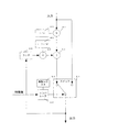
本実施の形態では、第1の実施の形態において説明したオーバーフロー処理を基本としてその改良を行った構成についてである。図31は、第8の実施の形態に係る画像表示装置の概略構成を示すブロック図である。
【0398】
なお本実施の形態のオーバーフロー処理の手法は第1の実施の形態に限るものではなく、他の実施の形態においても適用することができるものである。
【0399】
本実施の形態では、フレームごとの補正画像データの最大値を検出する最大値検出手段20と、最大値検出手段20の出力であるフレームごとの補正画像データの最大値を入力し、高域を遮断する(フレーム間の最大値の大きな変動を抑える)フィルタ手段40と、フィルタ手段40の出力を受け加算器12の出力が変調手段の入力範囲に収まるようなゲインを算出するゲイン算出手段21、及び算出されたゲインと、加算器の出力を乗算する乗算器によって、フレームごとにゲインを算出することにより、オーバーフローを防止している。
【0400】
この際に、表示画像のシーンが変わったことを検出する手段として以下に述べるような特徴量算出手段60を備えた。
【0401】
また、特徴量算出手段(シーン切り替え判別部)60の判別結果に基づいて下記に示すようにフィルタの動作を行うことにより好ましい表示を行うことができた。
【0402】
(特徴量算出手段(シーン切り替え判別部))
本実施の形態の特徴量算出手段60は、図31に示すように、各部と接続されている。
【0403】
特徴量算出手段60は、1フレーム分の画像データの平均輝度レベル(APL)を算出しさらにフレーム間の差分をとり絶対値を計算する手段である。
【0404】
平均輝度レベル(APL)算出は、加算器とレジスタなどによって構成できる回路である。平均輝度レベル(APL)算出は、レジスタに記憶されている値と、順次転送されてくる画像データを加算して再度レジスタに記憶する。そして順次、入力される画像データを加算する。
【0405】
レジスタの値は、フレームの先頭で0にクリアすれば、フレームの終了時にはそのフレーム内の画像データの加算値(1フレームの画素数は固定であるので、平均値に比例した値)が求まる。この値は平均輝度レベル(APL)となる。本実施の形態において、平均輝度レベル(APL)の最大値は255であるとする。
【0406】
次に、フレーム間の平均輝度レベル(APL)の差分を計算し、さらに絶対値を計算する。
【0407】
そして、特徴量算出手段60は、前記フレーム間の平均輝度レベル(APL)の差分の絶対値を出力する。
【0408】
(フィルタ手段)
本実施の形態のフィルタ手段40は、図31に示すように、最大値検出手段20の出力と、特徴量算出手段60の出力を入力し、後述する処理を行いゲイン算出手段21に出力する。
【0409】
フィルタ手段40の詳しい構成を図32に示す。
【0410】
図32において、41、42は乗算器、43は加算器、44はディジタルフィルタの遅延素子にあたるラッチ回路、45,46及び53は係数レジスタ、51はスイッチ、52はコンパレータである。
【0411】
上記構成において、フィルタ手段40の動作を説明する。
【0412】
(1)コンパレータ52に入力される特徴量算出手段60の出力(APLのフレーム間差分の絶対値)が係数レジスタ53の値以下の場合、スイッチ51の出力としてコンパレータ52の出力によって加算器43の出力が選択され、加算器43の出力が、フィルタ手段40の出力ならびにラッチ44への出力となる。
【0413】
この場合、係数レジスタ45,46、並びに、乗算器41,42、加算器43、ラッチ回路44は再帰型ディジタルフィルタを構成する。
【0414】
すなわち、現在の補正画像データの最大値は、乗算器41により係数レジスタ45に格納されている係数1/aが乗算される。
【0415】
一方、1フレーム前のフィルタ手段40の出力はラッチ回路44に格納され、係数レジスタ46に格納されている係数(1−1/a)が乗算器42により乗算される。
【0416】
これら二つの乗算結果を加算器43によって加算する。
【0417】
本発明者は、以上のフィルタ手段においてa=64としたものを用いて、ローパスフィルタを実現した。
【0418】
なお、係数レジスタ45,46は上述した値でなくても、ローパスフィルタを形成できればどのような値であっても良い。上述した値で構成した場合、乗算器41,42で扱う乗算係数の自然数aを2のn(nは自然数)乗とすると、ビットシフトと減算によって同等の計算がハードウエア化でき、回路規模を、少なくすることができる。
【0419】
(2)コンパレータ52に入力される特徴量算出手段60の出力(APLのフレーム間差分の絶対値)が係数レジスタ53の値より大きな場合(後述するが、シーンが変わったと判断したときである)、スイッチ51の出力としてコンパレータ52の出力によってフィルタ手段40の入力が選択され、フィルタ手段40の入力が、フィルタ手段40の出力並びにラッチ回路44への出力となる。
【0420】
すなわちフィルタ手段40は、
・フィルタ手段40に入力された補正画像データの最大値をそのまま出力する。
【0421】
・ラッチ回路44の内容を補正画像データの最大値に置き換える。
【0422】
以上の動作を行う。
【0423】
(フィルタ手段の他の実施の形態)
本実施の形態のフィルタ手段40の他の実施の形態を次に説明する。
【0424】
フィルタ手段40の他の実施の形態を図33に示す。
【0425】
図33において41a,41b,41c,41d,41eは乗算器、43aは加算器、44a,44b,44c,44dはディジタルフィルタの遅延素子にあたるラッチ回路、45a,45b,45c,45d,45e,53は係数レジスタ、52はコンパレータである。
【0426】
図33において、フィルタ手段40の他の実施の形態の動作を説明する。
【0427】
(1)コンパレータ52に入力される特徴量算出手段60の出力(APLのフレーム間差分の絶対値)が係数レジスタ53の値以下の場合、コンパレータ52は出力せず、乗算器41a,41b,41c,41d,41eと、係数レジスタ45a,45b,45c,45d,45eと、加算器43aと、ラッチ回路44a,44b,44c,44dは非再帰型ディジタルフィルタを構成する。
【0428】
では説明のため遅延素子の少ない(タップ数の少ない)フィルタの例を示したが、実際は16から128タップ程度、好ましくは30〜90タップ程度のフィルタが視覚的に良好であった。図32で説明した再帰型のディジタルフィルタ同様に、図33のディジタルフィルタも、係数レジスタ45a、45b、45c、45d、45eの値として、ローパス特性を持つものを使用した。
【0429】
(2)コンパレータ52に入力される特徴量算出手段60の出力(APLのフレーム間差分の絶対値)が係数レジスタ53の値より大きな場合(後述するが、シーンが変わったと判断したときである)、コンパレータ52は、ディジタルフィルタの遅延素子であるラッチ回路44a,44b,44c,44dのロードパルス(Ld)を出力する。
【0430】
そして、ラッチ回路44a,44b,44c,44dの内容を入力されたデータに置き換える。そして、フィルタ手段40に入力された補正画像データの最大値をそのまま出力する。
【0431】
そして、図32で示したディジタルフィルタ回路と同等の動作を行う(係数レジスタ45a,45b,45c,45d,45eの総和は1となるように選ぶ。)。
【0432】
(ゲイン算出手段(ゲイン算出部))
ゲイン算出手段21は、補正画像データDoutが変調手段の入力範囲に収まるようにゲインを算出する手段である。
【0433】
本実施の形態ではゲインはフィルタ手段40の出力をMAX’、定数をKf1とすると
【数22】
【0434】
上式では、多少オーバーフローが発生しても、自然画などのではゲインを大きめにした場合、明るく表示できるので主観的にきれいに見えることを示している。
【0435】
本実施の形態では、
Kf1=1
と本発明者らは決定し、良好な画像を得ることができた。
【0436】
本実施の形態でもゲインは1フレーム毎にゲインの値が変更される。
【0437】
なお、本実施の形態では、フレーム単位でのゲインの変動を抑えるためのフィルタを設けたことにより、厳密にはオーバーフローが起きることがある。
【0438】
このような課題に対し、補正画像データとゲインを乗算する乗算器の出力に対し後述するリミッタ手段を設け、乗算器の出力が変調手段の入力範囲に収まるように回路を設計した。
【0439】
(オーバーフロー処理の動作)
(1)フリッカの低減
オーバーフロー処理を行う場合、前述したようにフレーム単位で輝度を明るくすることができる。
【0440】
フィルタ手段40がない場合は、以下のような妨害感(フリッカ)が発生する場合があった。
【0441】
例えば、わかりやすい例として、下半分海で上半分空のような画像で、下半分海の部分のさざ波により太陽の反射光がきらきらしているシーンを考える。
【0442】
この場合、波のうねりにより太陽の反射光がきらきらしている部分に対応して補正画像データの最大値が小刻みに変化する。前述したようにフレーム単位でゲインを決定する場合、ゲインがフレーム単位で小刻みに変化するため、オーバーフロー処理した画像は、特に空部分の明るさがゲインの変化に応じて小刻みに変化し妨害感(フリッカ)が発生する。
【0443】
本実施の形態で示した構成では、オーバーフロー処理を行う場合、フィルタ手段40によって高域を除去し、最大補正画像データの変化を緩やかにする。
【0444】
そのため、上記のような、小刻みに補正画像データの最大値が変化するような画像であってもゲインが緩やかな変化となり、妨害感を発生せず輝度を上げることができる。
【0445】
前述したように、妨害感(フリッカ)を除去するためには、最大補正画像データの小刻みな変化を除去するローパスフィルタを用いたが、カットオフ周波数を下げすぎると実際に追従したいゲイン変化もしなくなる。
【0446】
そのため本発明者らが確認したところ、前述した図32の再帰型のフィルタにおいて、a=128または、a=64または、a=32または、a=16が良好であった。特に、a=64またはa=32が、主観評価の結果最適であった。また図33で示した非再帰型のフィルタでは16から128タップ程度が良好であり、特に30から90タップが主観的に良好であった。
【0447】
実際の画像データのフレーム番号対補正画像データの最大値(最大補正画像データ)のグラフを図34に示す。また、同じ画像のフレーム番号対本発明のフィルタ手段40の出力(図32の再帰型フィルタでa=64時)のグラフを図35に示す。両グラフを見てもわかるようにゲインの小刻みの変動が抑えられていることがわかる。図35は説明を簡単にするため係数レジスタ53の値が大きく(例えば絶対値が255相当)、シーンチェンジを行わない場合の例を示した。
【0448】
(2)シーンチェンジにおける違和感の低減
上述した画像において、妨害感(フリッカ)をなくすことができた。
【0449】
しかしながら、画像が、あるシーンから次のシーンへ移るとき(シーンチェンジ)、妨害感が発生する場合があった。
【0450】
具体的には、例えば白い砂浜のような明るいシーンから、夜空のような暗いシーンにシーンチェンジした場合を説明する。
【0451】
白い砂浜のシーンでは画像データが大きく、前述したように補正画像データも大きな値である、そのためゲインは小さな値となる。
【0452】
次に、夜空のような暗いシーンに変わった直後では、画像データは小さくさらに前述したように補正画像データも小さな値である(大きなゲインとなる)。しかし、フィルタ手段40により補正画像データにはローパスフィルタがかかるので、フィルタ手段40の出力は現在の最大補正画像データより大きな値となり、ゲインは小さな値となる。
【0453】
その後、時間の経過とともに(数秒)ゲインが大きな値に変化していく。
【0454】
そのため、夜空のような暗いシーンに変わった直後はとても暗く、数秒間でだんだん明るく表示され、画像を見ている人にとって違和感が生じていた。
【0455】
上記違和感を除去するために、本実施の形態において、上述したフィルタ手段40のローパスフィルタの特性は、特徴量算出手段60の出力(APLのフレーム間差分の絶対値)が係数レジスタ53の値より大きな場合に、
・フィルタ手段40に入力された最大補正画像データをそのまま出力する
・ラッチ回路44の内容を最大補正画像データに置き換える
ことを、行う。
【0456】
実際の係数レジスタ53の値として、特徴量算出手段60の出力(APLのフレーム間差分の絶対値)の最大値が255の時(APLの最大値が255の時)に20〜5の範囲、特に10の値が最適であった。
【0457】
すなわち、APLのフレーム間の差が10以上のときはシーンチェンジとみなしローパルフィルタの遅延素子の内容を入力データに変更し、ゲインの追従性をあげた。
【0458】
図34で示した画像のフレーム番号対APL値のグラフを図36に示す。係数レジスタ53の値が10の時の、フレーム番号対フィルタ手段40の出力(図32の再帰型フィルタでa=64時)のグラフを図37に示す。両図において、入力される画像は240フレームごとにシーンの異なる動画像である。図37を見てわかるように、シーンチェンジ時、フィルタ手段の出力は追従性よく変化し、さらにフリッカが抑えられているのがわかる。実際に表示された画像もフリッカ妨害感や、シーンチェンジ時の違和感が無く良好であった。
【0459】
ここで、入力画像データを逆ガンマ変換する前のデータを特徴量算出手段60に入力したが、逆ガンマ処理部の出力を特徴量算出手段60に入力し、平均輝度レベル(APL)のフレーム間差分を算出しても同様の効果が得られた。
【0460】
(第9の実施の形態)
本発明の第9の実施の形態として、図38に示す構成を説明する。
【0461】
第8の実施の形態においては、フィルタ手段40を最大値検出手段20の出力に対して備え、フィルタ手段40の出力値に対してゲインを算出する構成であったが、本実施の形態においては、最大値検出手段20の出力からゲイン算出手段21でゲインを算出し、算出したゲインに対してフィルタ手段40を備える構成とした。
【0462】
すなわち、フィルタ手段40においてゲインの変動を抑える処理を行う構成である。その他の各構成、及びフィルタ手段40の構成は第8の実施の形態と同様とすることで、好適な補正画像データを表示することができた。
【0463】
(第10の実施の形態)
第10の実施の形態においては、図39に示すように接続し、特徴量算出手段60は、入力された画像データの1フレーム単位のAPLのフレーム間差分の絶対値と、補正画像データの最大値MAXのフレーム間差分の絶対値の両方を算出する構成とした。
【0464】
またフィルタ手段40内には、図40に示すように、APLのフレーム間差分の絶対値を判定するためのコンパレータ52aと係数レジスタ53a、MAXのフレーム間差分の絶対値を判定するためのコンパレータ52bと係数レジスタ53b、二つの判定結果を参照するための判定手段54を用意した。本実施の形態においては、判定手段54をOR回路とした。他の構成は、ここまでの実施の形態と同じである。
【0465】
特徴量としてAPLのフレーム間差分のみを扱っていた場合、例えば黒い画面の1/3に白ベタの横ラインが表示されている画面(MAXは大きくなる)から画面全体に単色ベタが表示されている画面(MAXは小さくなる)に切り替わった時(両者のAPL値は同じ)にシーンチェンジと判定されず、数秒間違和感が現れてしまう。本実施の形態においては、この場合もMAXのフレーム間差分の判定によりシーンチェンジと判断され、良好な画像を得ることができた。
【0466】
また、本実施の形態においても、APLのフレーム間差分の絶対値を算出する際に、逆ガンマ処理部の出力を扱っても同様の効果が得られた。
【0467】
(第11の実施の形態)
これまでいくつかの実施の形態をもとに本発明の画像表示装置について説明してきた。
【0468】
一方、上記のすべての実施の形態に共通する問題として、入力される画像の品質に応じて下記のような問題が発生することがあった。
【0469】
入力画像データにノイズが乗っており、そのノイズを含んだ入力画像データに対して補正を行った場合、補正の結果として算出される補正画像データにおいてもノイズが乗ってしまうために、ノイズによってゲインがフレーム単位で変動し、表示画像の明るさがちらつく(フリッカがおこる)場合があった。
【0470】
本発明者らは検討した結果、このようなノイズは、
1)放送局で作られた画像の周辺部分、
2)スケーラなどを行って作成した画像の周辺部分、
3)インターレース信号をプログレッシブ信号に変換するI/P変換機の出力画像の周辺部であって、特に画像の上下数水平走査ラインの映像データ、
などの画像に多く発生していることがわかっている。
【0471】
画像1)〜3)は一例ではあるが、これらの場合、画像の周辺部分という特定の位置にノイズが多く発生していることがわかってきた。そしてこのノイズによりゲインが変化し表示画像に妨害感を与えていた。
【0472】
画像1)〜3)の原因は元画像を変換した場合に多く発生する。すなわち、元画像をフィルタ演算して新しい画像を生成する際、画像の周辺部(特にエッジ部分)はフィルタ演算の入力に元画像がない状態で処理しなくてはならない。そのため無いデータに対応する処理の違いなどから、画像の周辺部(特にエッジ部分)の画像データの値が劣化する(ノイズが発生する)場合が多い。
【0473】
特に、3)のI/P変換機の出力画像は、奇数フィールドと偶数フィールドでフィルタ演算する元画像が1水平ラインずれているので、元画像のフィールド単位すなわちI/P変換後のフレーム単位で、画像の上下水平ライン画像データの値が変化する。
【0474】
そして、3)の場合、ノイズに対する補正画像データが、最大値検出手段20において最大値として検出されると、そのノイズがフレーム単位で変化し、ゲインがフレーム単位で変動し、表示画像の明るさがちらついた(フリッカ)。
【0475】
一例として、後述する本発明の範囲選択手段400がない場合に、インターレース信号をプログレッシブ信号に変換するI/P変換機のからのある出力画像に対して補正を行ったときの最大値検出手段20からの出力を図41に示す。
【0476】
ある連続した入力画像データの最大補正画像データが、1フレームごとに大幅に変動している。これはすなわち、1フレームごとに大幅にゲインが変わり、フリッカとして出力画像に現れてしまうことを表している。
【0477】
前述したように、この原因となっているノイズは、元画像をフィルタ演算して新しい画像を生成する際に画像の周辺部(特にエッジ部分)に現れることがある。
【0478】
そのため本発明者らは、以下に示す範囲選択手段400を設けた。図42において400は範囲選択手段、20は最大値検出手段である。
【0479】
なお本実施の形態のオーバーフロー処理は第1の実施の形態の構成を例にとって説明しているが、他の実施の形態のオーバーフロー処理の形態においても適用できることはいうまでもない。
【0480】
範囲選択手段400は、例えば図43に示すように構成でき、401、402、403、404はそれぞれレジスタA1、A2、B1、B2である。405、406、407、408はそれぞれコンパレータA1、A2、B1、B2である。409はデコーダ、410はスイッチ、411はレジスタCである。
【0481】
レジスタA1(401)には最大値として検出したい補正画像データの垂直範囲の最小値が記憶されており、コンパレータA1(405)によりDoutの垂直位置情報である入力値Yと比較し、Yの方が大きい時に選択信号を発生する。
【0482】
一方、レジスタA2(402)には最大値として検出したい補正画像データの垂直範囲の最大値が記憶されており、コンパレータA2(406)によりDoutの垂直位置情報である入力値Yと比較し、Yの方が小さい時に選択信号を発生する。
【0483】
さらに、レジスタB、コンパレータBは水平位置についての選択部であり、上記レジスタA、コンパレータAと同様の構成とした。
【0484】
これらの選択信号から、AND回路等によって構成されるデコーダ409は、検出したい範囲内の補正画像データがDoutとしてスイッチ410に入力されている時の選択信号を発生する。レジスタC(411)には、例えば0が格納されており、スイッチ410は選択信号が発生しているときはDoutをスルーし、発生していないときは0を出力する構成とした。
【0485】
具体的に補正画像データの最大値を検出する範囲としては、前述したノイズを十分除去できるとともに、表示画像の特徴を取り入れることができる範囲として選択され、例えば、表示領域の上下の端部から、1本以上且つ全行配線数の1/10以下の本数の行配線に対する補正画像データを除いて、それ以外の中央部の行配線に対する補正画像データを選択することが好ましい。
【0486】
特に3)のI/P変換機の出力画像を入力する時、選択手段は、全行配線数を768本として、画像の上下水平ライン数本(1本以上10本以下)にあたる出力を0にするのみでも有効である。
【0487】
図44は、範囲選択手段400を用い、図41に示した画像データを入力した時の最大値検出手段20の出力を示している。
【0488】
図44から、最大補正画像データの1フレームごとの大幅な変動(すなわちゲイン変動)がなくなっているのがわかる。以上のように表示画像のフリッカの発生を防止できた。
【0489】
また、他の実施の形態として、範囲選択手段400を、例えば、図45に示す構成としても同様の効果が得られた。図45において412は乗算器、413はメモリである。メモリ413は、最大値として検出したくない補正画像データを小さい値にするための重みを、補正画像データの位置をアドレスとして格納したものであり、入力された補正画像データとメモリ413からの出力を乗算器412によって順次乗算して出力とした。例えば上下端付近の補正画像データを最大値として検出したくない場合、図46に示すような上下端を0、中央部を1とした滑らかな凸状の重みをメモリ413に格納すればよい。
【0490】
画像表示装置外においてI/P変換された画像など、前述したノイズの乗った画像も多く存在するため、以上説明した構成によって、最大補正画像データのノイズによる変動、すなわちゲイン変動を好適に抑えることが可能となった。
【0491】
(第12の実施の形態)
本発明における第12の実施の形態として、図47に示すように、補正データ算出手段14の出力に対して範囲選択手段400を備えた構成としても同様の効果が得られた。
【0492】
図47において、14は補正データ算出手段、400は範囲選択手段である。この場合、最大値として検出したくない位置の入力データに対しては補正データの加算を行わない、あるいは補正データを小さく重み付けし加算するように、範囲選択手段400によって、補正データを選択しない、あるいは重みをかけるといった処理が行われる。その他の各構成は第11の実施の形態と同様とすることで、好適な補正画像データを表示することができた。
【0493】
(第13の実施の形態)
本発明における第13の実施の形態として、図48に示す構成を説明する。20は最大値検出手段、21はゲイン算出手段、22R,22G,22Bは乗算器である。ここでは、ゲイン算出手段21によって算出されたゲインを、逆γ処理部17から出力であるRa、Ga、Baにフィードバックして乗算器22R,22G,22Bによって乗算する構成とした。すなわち、補正する前のデータに対して、補正後も変調手段8の必要とする入力範囲に収まる値になるよう、予め縮めておく構成である。その他の各構成は第11、第12の実施の形態と同様とすることで、好適な補正画像データを表示することができた。
【0494】
(第14の実施の形態)
本発明における第14の実施の形態として、図49に示す構成を説明する。本実施の形態では第12の実施の形態のように範囲選択手段400を接続し、第13の実施の形態のようにゲイン算出手段21によって算出されたゲインを、逆γ処理部17からの出力であるRa、Ga、Baにフィードバックして乗算器22R,22G,22Bによって乗算する構成である。その他の各構成は第11〜第13の実施の形態と同様とすることで、好適な補正画像データを表示することができた。
【0495】
(第15の実施の形態)
発明者らはこれまで述べてきたようなオーバーフロー処理において入力される画像によっては、以下のような問題点が生じることがわかってきた。
【0496】
以下、第1の実施の形態のオーバーフロー処理を例にとって説明を行う。なお、本実施の形態のオーバーフロー処理は第1の実施の形態を例にとって説明するが、他の実施の形態においても適用することができることはいうまでもない。
【0497】
たとえば、変調手段への入力ビット数が8ビットであって、補正画像データDoutのビット数が9ビットの時、あるフレームの補正画像データの最大値すなわち最大値検出手段の出力が255以上の時はゲインは1倍以下となり、補正画像データDoutに1倍以下のゲインを乗じることによる画質低下の問題はほとんど認知されない。
【0498】
しかしながら、夜景のような画面全体が暗い画像が入力された場合、そのフレームの補正画像データの最大値は小さな値になる。例えば、一例として補正画像データの値が25であったとすると、この時ゲインの値は約10(=255/25)になる。このゲインを補正画像データDoutに乗じると、以下の問題が生じた。
【0499】
第1に、本来暗い画像が、非常に明るく表示されてしまう、第2に、表示分解能がゲイン倍され粗くなり擬似輪郭が目立つ、という問題である。このため、表示画像の質が著しく低下する。すなわち、ゲインが大きな値の場合に上記問題が生じることになる。
【0500】
図50は、第15の実施の形態に係る画像表示装置の概略構成を示すブロック図である。
【0501】
本実施の形態においては、先に述べた表示画像の悪化を防止するために、後述するように、フレームごとの補正画像データの最大値を検出する最大値検出手段901と、加算器の出力(補正画像データ)が変調手段の入力範囲に収まるようなゲインを算出するゲイン算出手段902、ゲイン算出手段から算出されたゲインの最大値を制限するゲイン制限部903、及びゲイン制限部の出力と補正画像データとを乗算する乗算器904によって、全体的に暗い入力画像に対してゲインが必要以上に大きくならないように制御し、明るい入力画像に対してはオーバーフローを防止することが可能となる。
【0502】
(最大値検出手段(最大値検出部))
本実施の形態の最大値検出手段901は、図50に示すように、各部と接続されている。
【0503】
最大値検出手段901は、1フレーム分の補正画像データDoutのなかで、最大となる値を検出する手段である。検出された補正画像データの最大値(最大補正画像データ)は、ゲイン算出手段902へと転送される。
【0504】
(ゲイン算出手段(ゲイン算出部))
ゲイン算出手段902は、補正画像データDoutが変調手段の入力範囲に収まるようにゲインを算出する手段である。
【0505】
ゲインの決定方法は、第1の実施の形態の構成では、式12や式13により決定してもよい。
【0506】
また、ゲインは、垂直帰線期間に更新して1フレーム毎にゲインの値が変更される。
【0507】
また、本実施の形態でも第1の実施の形態と同様に、補正画像データとゲインを乗算する乗算器の出力に対し後述するリミッタ手段905を設けてもよい。
【0508】
(ゲイン制限部)
図50において、ゲイン制限部903はゲイン算出手段902で算出されたゲインの最大値を制限し乗算器904に出力する。
【0509】
ゲイン制限部903の構成はリミッタ回路(ゲインリミッタとも記す)であり、具体的な構成は図51に示すとおりである。
【0510】
ゲイン算出手段902の出力は、比較器9032の入力とスイッチ9033の接点aに入力される。比較器9032の他方の入力とスイッチ9033の接点bにはゲイン制限レジスタ9031からの出力が接続される。
【0511】
ゲイン制限レジスタ9031には予め最大ゲイン値が記憶されており、この最大ゲイン値とゲイン算出手段902で算出されたゲインとを比較器9032は比較し、ゲイン算出手段902で算出されたゲインがゲイン制限レジスタ9031に記憶されている最大ゲイン値より大きければ、スイッチ9033は接点bを選択し、ゲイン制限レジスタ9031に記憶されている最大ゲイン値を出力する。
【0512】
一方、ゲイン算出手段902で算出されたゲインがゲイン制限レジスタ9031に記憶されている最大ゲイン値より小さければ、スイッチ9033は接点aを選択し、ゲイン算出手段902で算出されたゲインを出力する。
【0513】
ゲイン制限レジスタ9031に記憶されている最大ゲイン値として0.5〜2程度が良好であり、とくに中でも、1としたところ良好であった。
【0514】
また、本発明者らは、上述したゲイン制限部903の構成以外に、図52のような構成によってゲインを制限してもよいことを確認している。
【0515】
図52において9034はゲイン制限テーブルであり、予めゲインの制限特性が記憶されているメモリ(ゲインテーブルメモリとも記す)である。
【0516】
ゲイン制限テーブル9034(ゲインテーブルメモリ)のアドレス線はゲイン算出手段902の出力に、ゲイン制限テーブル9034(ゲインテーブルメモリ)のデータ線は乗算器904に接続される。
【0517】
前記ゲインの制限特性は、例えば、図51で示したゲイン制限部903の特性を実現するためには図53(a)の特性をゲイン制限テーブル9034に記憶させておく(本例では最大ゲイン値を1としたが、0.5〜2の中から選ぶと良好である)。
【0518】
また、前記ゲインの制限特性を、図53(b)の特性のようになだらかに制限すると、さらに画像を良好に表示できた(本例では最大ゲイン値を1としたが、0.5〜2の中から選ぶと良好である)。
【0519】
本実施の形態ではゲイン算出手段902と、ゲイン制限部903をまとめて制限ゲイン算出手段と呼ぶ。
【0520】
制限ゲイン算出手段において、ゲイン算出手段902は最大値検出手段901で求めた1フレーム分の補正画像データDoutの中の最大値(最大補正画像データ)を入力とし、補正画像データDoutが変調手段の入力範囲に収まるために乗算すべきゲインを算出した。
【0521】
次に、ゲイン算出手段902で算出されたゲインの最大値を、ゲイン制限部903は制限し乗算器904に出力した。
【0522】
また、制限ゲイン算出手段は以下の構成であっても同様の効果が得られる。
【0523】
制限ゲイン算出手段は、最大値検出手段901で求めた1フレーム分の最大補正画像データに対し、その最小値を制限(最小値の下限を設定)する手段(不図示の補正画像最大値制限手段)を設ける。さらに、補正画像最大値制限手段の出力をゲイン算出手段902でゲインに算出する。
【0524】
不図示の補正画像最大値制限手段の実施の形態は、前出のゲイン制限部903の構成とほぼ同じであるので図は省略する。
【0525】
以上、本実施の形態の画像表示装置を用いれば、通常の画像では、走査配線に生じる電圧降下の影響を補正し、かつ表示画像の輝度を上げることができる。また平均輝度が低い画像が入力された場合には、走査配線に生じる電圧降下の影響を補正し、暗い画像が非常に明るく表示されてしまうことや、この時表示分解能がゲイン倍され粗くなり擬似輪郭が目立つことを防止でき、非常に好ましかった。
【0526】
(第16の実施の形態)
本発明者らは、これまで述べてきたようなオーバーフロー処理において、さらに検討を行ったところ、特徴量算出手段(シーン切り替え判別手段)としては以下のような処理を行う方がより精密に判別することができることを確認した。
【0527】
(特徴量算出手段(シーン切り替え判別部))
本実施の形態の特徴量算出手段60は、図54に示すように、各部と接続されている。
【0528】
図55に示す特徴量算出手段60は、所定エリアごとに1フレーム毎の画像データの部分平均輝度レベル(L_APL)を算出し、さらにフレーム間の差分をとり絶対値を計算し、各エリアの計算結果をそれぞれ所定値と比較した結果を加算する手段である。
【0529】
本実施の形態においては、所定エリアとして3箇所選んだ構成を説明する。
【0530】
図55において、61a,61b,61cはエリア判定手段、62a,62b,62cはラッチ、63a,63b,63cは差分算出手段、64a,64b,64cはコンパレータ、65a,65b,65cは係数レジスタ、66a,66b,66c,67は加算器である。
【0531】
加算器66a,66b,66cにおいて、それぞれラッチ62a,62b,62cに記憶されている値と、順次転送されてくる画像データを加算して再度ラッチ62a,62b,62cに記憶する。そして順次、入力される画像データを加算する。
【0532】
ここで、エリア判定手段61a,61b,61cは、入力された画像データの位置情報と、それぞれの内部に格納された所定エリア情報を比較し、一致している時にそれぞれラッチ62a,62b,62cに対してenable信号を出力する。
【0533】
ラッチ62a,62b,62cの値は、フレームの先頭で0にクリアすれば、フレームの終了時にはそのフレーム内の画像データの加算値(1フレームの各エリアの画素数は固定であるので、平均値に比例した値)が所定エリアごとに求まる。この値は各所定エリアの部分平均輝度レベル(L_APL)となる。
【0534】
次に、差分算出手段63a,63b,63cにおいて、所定エリアごとにフレーム間の部分平均輝度レベル(L_APL)の差分を計算し、さらに絶対値を計算する。
【0535】
そして、各所定エリアの絶対値をそれぞれコンパレータ64a,64b,64cにより、係数レジスタ65a,65b,65cに格納された所定値と比較し、所定値より大きければ各所定エリアにおいて部分的にシーンチェンジがあったとして1を出力する。各所定エリアの絶対値が各所定値より小さい時は0を出力する。
【0536】
さらに加算器67において各コンパレータ64a,64b,64cの出力を加算し、特徴量算出手段60の出力とする。したがって、特徴量算出手段60の出力はシーンチェンジと判断されたエリアが多いほど大きい値となる。
【0537】
(判定手段)
本実施の形態の判定手段80は図54に示すように、特徴量算出手段60の出力を入力し、所定の値と比較した結果を後述するフィルタ手段40に出力する。
【0538】
判定手段80の構成を示した図56において、83は係数レジスタ、84はコンパレータである。
【0539】
特徴量算出手段60からの出力を、コンパレータ84により係数レジスタ83に格納された所定値と比較し、入力値が所定値より大きければシーンチェンジであるとしてHighが出力される。
【0540】
ここで、特徴量算出手段60に備えた加算器67は、AND回路やOR回路を組み合わせたものとしてもよく、この場合には判定手段80は不要となるが、AND回路やOR回路の組み合わせを複雑にする必要がある。
【0541】
(シーンチェンジの判定)
上述したように、シーンチェンジ判定によってフィルタ手段40の出力を変更することで違和感が除去できたが、フレーム間の画面全体の平均輝度(APL)の変化によってシーンチェンジを判定した場合、シーンチェンジの誤検出が生じる場合があった。
【0542】
具体的には同一の背景に対して画面下に白い文字でテロップが現れた時であった。この場合、テロップによって画面全体の平均輝度(APL)が上がり、それに応じてシーンチェンジと判断されたため、テロップが現れた直後に急激に画面が暗くなってしまっていた。
【0543】
この現象を防ぐために本実施の形態においては、特徴量算出手段60における所定エリアとして、画面を上下に3分割したエリアを格納し、それぞれのエリア内の部分平均輝度(L_APL)を算出する構成とした。
【0544】
本構成によれば、テロップが現れた時に変化するのは画面下のエリアの部分平均輝度(L_APL)のみとなり、加算器67の出力(すなわち特徴量算出手段の出力)は1となる。したがって、係数レジスタ83aの値として、2を格納しておくことで、シーンチェンジの誤検出が防げた。
【0545】
ここで、実際の各係数レジスタ65a,65b,65cに格納した値として、差分検出手段63a,63b,63cの最大値が255の時に5〜20の範囲、特に10の値が最適であった。
【0546】
以上に述べた構成によって実際に表示された画像は、シーンチェンジが誤検出されることなく、フリッカ妨害感やシーンチェンジ時の違和感が除去され、良好であった。
【0547】
なお、上記の例においては、簡単のため横のテロップに対する違和感を除去する構成を述べたが、縦のテロップが現れるシーンにおける違和感の除去には、エリアを左右に区切れば効果的であった。実際にはそれらの複合による違和感を除去するために、位置情報で細かく区切ったエリアを採用すると効果的であった。また、各エリアは必ずしも独立している必要は無かった。
【0548】
また、逆ガンマ処理部の出力を特徴量算出手段60に入力し、各エリアの部分平均輝度レベル(L_APL)のフレーム間差分に基づいて判定しても同様の効果が得られた。
【0549】
また、補正画像データを特徴量算出手段60に入力し、各エリアの部分平均輝度レベル(L_APL)のフレーム間差分に基づいて判定しても同様の効果が得られた。
【0550】
また、特徴量算出手段60の構成を図57に示すようにし、補正画像データを特徴量算出手段60に入力し、各エリアの部分最大値のフレーム間差分に基づいて判定しても同様の効果が得られた。
【0551】
図57において、61a,61b,61cはエリア判定手段、62a,62b,61cはラッチ、63a,63b,63cは差分算出手段、64a,64b,64c,66a,66b,66cはコンパレータ、65a,65b,65cは係数レジスタ、67は加算器である。
【0552】
コンパレータ66a,66b,66cにおいて、それぞれラッチ62a,62b,62cに記憶されている値と、順次転送されてくる補正画像データを比較して大きい方の値を再度ラッチ62a,62b,62cに記憶する。そして順次、入力される画像データを比較する。
【0553】
ここで、エリア判定手段61a,61b,61cは、入力された補正画像データの位置情報と、それぞれの内部に格納された所定エリア情報を比較し、一致している時にそれぞれラッチ62a,62b,62cに対してenable信号を出力する。ラッチの値は、フレームの先頭で0にクリアすれば、フレームの終了時にはそのフレーム内の補正画像データの部分最大値が所定エリアごとに求まる。
【0554】
次に、差分算出手段63a,63b,63cにおいて、所定エリアごとに部分最大値の差分を計算し、さらに絶対値を計算する。
【0555】
そして、各所定エリアの絶対値をそれぞれコンパレータ64a,64b,64cにより、係数レジスタ65a,65b,65cに格納された所定値と比較し、所定値より大きければ各所定エリアにおいてシーンチェンジがあったとして1を出力する。各所定エリアの絶対値が各所定値より小さい時は0を出力する。
【0556】
さらに、加算器67において各コンパレータ64a,64b,64cの出力を加算し、特徴量算出手段60の出力とする。したがって、特徴量算出手段60の出力はシーンチェンジと判断されたエリアが多いほど大きい値となる。
【0557】
また、特徴量算出手段60は、メモリとして各エリアの算出値を格納するアドレスを確保し、CPUによって判定や計算を行う構成としても同様の効果が得られた。
【0558】
以上説明したように、本実施の形態によれば電圧降下補正を行った際のオーバーフロー処理を行う際に発生する場合がある妨害感(フリッカ)やシーンチェンジ時の違和感を、低減することが可能となり、画像の品質を良好にすることができた。
【0559】
(第17の実施の形態)
本発明者らは、これまで述べてきたようなオーバーフロー処理において、さらに検討を行ったところ、以下のようにゲインを算出する処理を行ったところさらに好ましいことを確認した。
【0560】
たとえば、第1の実施の形態に示したようなオーバーフロー処理を例とすると、オーバーフロー処理として補正画像データに乗算するためのゲインGとしては以下に示すようなことがわかってきた。
【0561】
A.オーバフローしないように計算されたゲインG以下の値を用いると、ゲインGの値に比例して輝度が変化する。ただしゲインGの値が小さい時は輝度が暗く、さらに階調性が悪くなる。
【0562】
B.オーバフローしないように計算されたゲインGより大きな値を用いると、ゲインGの値に従って輝度が増加する。ただしゲインGの値が大きな時は前記リミッタ905により忠実に画像を表示できなくなる。
【0563】
さらに、このようなゲインGを補正画像データDoutに乗算して画像を表示する検討をしていくと、外部環境、特に画像表示する場所の照度によって、主観的な表示画像に対する評価値が変化することがわかってきた。
【0564】
すなわち、
C.画像表示する場所の照度が基準値より低い時(暗い部屋で画面を見る時)、画面の輝度がより高くなるように表示するより(すなわち明るく表示するより)、前記走査配線の影響による画質劣化を正確に補正した方が、主観的な表示画像に対する評価値が良くなった。
【0565】
D.画像表示する場所の照度が基準値より高い時(明るい部屋で画面を見る時)、前記走査配線の影響による画質劣化を正確に補正するより、画面の輝度がより高くなるように表示する方が(すなわち明るく表示する方が)、主観的な表示画像に対する評価値が良くなった。
【0566】
ここで、基準値とは、必ずしも一義的に決定されるものではないが、画像表示装置の特性や、その使用者、使用分野等を勘案して、最適な値を基準値とすればよい。例えば、画像表示装置が最も使用される環境における照度を基準値とすることが考えられる。
【0567】
このような、構成的な特徴と主観的な評価から、本発明者らは以下のような構成で前記ゲインを補正画像データに乗算して画像を表示することによって良好な表示画像を得ることができた。
【0568】
図58は、第17の実施の形態に係る画像表示装置の概略構成を示すブロック図である。
【0569】
すなわち、前記構成に加え、外部環境を入力する外部環境入力手段906と、外部環境入力手段906の出力をKGAINに変換するKGAINテーブル(変換手段)907を有し、さらに、ゲイン算出手段902は、最大値検出手段901の出力と前記KGAINから後述するようにゲインGを算出し、さらに、算出されたゲインGと、補正画像データの出力を乗算する乗算器によって、フレームごとにゲインを算出し、変調手段の入力データを計算することによって、良好な表示画像を得ることができた。
【0570】
詳細は、以下に説明する。
【0571】
(最大値検出手段(最大値検出部))
本発明の最大値検出手段は図58に示すように、各部と接続されている。
【0572】
最大値検出手段901は、1フレーム分の補正画像データDoutのなかで、最大となる値を検出する手段である。
【0573】
検出された補正画像データの最大値(最大補正画像データ)は、ゲイン算出手段902へと転送される。
【0574】
(ゲイン算出手段(ゲイン算出部))
ゲイン算出手段902は、補正画像データDoutに乗算する乗数(ゲインG)を算出する手段である。ゲイン算出手段902の実際の計算式の一例を、以下に示す。
【0575】
ゲインの決定方法は、1フレーム内で、最大値検出部で検出した加算器の出力データの最大値をMAX、変調手段の入力範囲の最大値をINMAX、後述するKGAINテーブル(変換手段)の出力をKGAINとすると、
【数23】
【0576】
この方法によりゲインGを決定すれば、KGAINの値を1より大きくすることによってゲインGを大きめにでき、表示画像の輝度を明るくすることができる。
【0577】
このゲイン算出手段902で求めたゲインGは、垂直帰線期間に更新して1フレーム毎にゲインの値が変更される。
【0578】
KGAINが1より大きい場合、乗算器904の出力は変調手段8の入力範囲の最大値を超えるデータがより多く発生する。後述するように、補正画像データにKGAINを乗じた補正画像データDmultはオーバフローを起こす。
【0579】
さらに、本実施の形態の画像表示装置の構成では、1フレーム前の補正画像データの最大値を用いて、現在のフレームの補正画像データに乗算するゲインを算出する構成となっている。
【0580】
従って、厳密には、フレームごとの補正画像データの違いから、オーバーフローが起きることがある。
【0581】
このように上記2つのオーバフローの原因に対して、KGAINを乗じた補正画像データDmult(乗算器の出力)に対し後述するリミッタ手段905を設け、乗算器904の出力が変調手段8の入力範囲に収まるように回路を設計した。
【0582】
前述した主観評価の結果C.から、表示装置が置かれている環境が暗いときは、表示画像は忠実度を高く(その代わり輝度を抑え)するようにKGAIN=1に設定する。
【0583】
また、前述した主観評価の結果D.から、表示装置が置かれている環境が明るいときは、輝度を上げ(その代わり表示画像の忠実度を下げ)るためにKGAIN=1〜2を設定する。
【0584】
以上のようにKGAINを設定することによって、主観的に良好な画像表示を行える。
【0585】
KGAINの具体的な作成法については後述する。
【0586】
(乗算器)
ゲイン算出手段902の出力と、補正画像データDoutは、図58の乗算器904によって乗算され、補正画像データDmultとしてリミッタ手段905へ転送される。乗算器904はいわゆるロジック回路によって構成してもよいし、テーブルメモリ(ROMまたはRAM)に乗算結果を格納しておいて、乗算する2つのパラメータをアドレスに入力し、データから乗算結果を出力してもよい。
【0587】
また、乗算器904の出力が接続されているリミッタ手段905もテーブルメモリで構成できることから、リミッタ手段905と、乗算器904をひとつのテーブルメモリによって構成することもできる。
【0588】
この場合、テーブルメモリに格納するべき内容は、乗算結果をリミットするデータが記載されていればよい。
【0589】
なお、好ましいリミッタの特性については以下に述べる。
【0590】
(リミッタ手段)
以上のようにして、ゲインGを決定するが、前述したように、しばしばオーバーフローが起きる。そのため、変調器がオーバーフローしないように、リミッタ(Limiter)を設けておく。
【0591】
リミッタ手段905は、予め設定されたリミット値を有し、リミッタ手段905に入力される出力データDmultとリミット値とを比較し、出力データDmultよりもリミット値が小さければ、リミット値を出力し、出力データDmultよりもリミット値が大きければ、出力データDmultを出力する(図58における信号名は補正画像データDlim)。
【0592】
リミッタ手段905は、図59(a)に示すように最大値まで一定の傾きの直線である折れ線の特性を示すものでもよいし、図59(b)に示すように最大値で飽和する飽和特性のような曲線の特性を示すものでもよい。図59(a)の特性のリミッタはコンパレータによって実現することができ、図59(b)の特性のリミッタはテーブルメモリなどにより実現することができる。
【0593】
リミッタ手段905によって、変調手段8の入力範囲に完全に制限された補正画像データDlimは、シフトレジスタ5、ラッチ6を介して変調手段8へと供給される。
【0594】
(外部環境入力手段)
外部環境入力手段906は、例えばCdS受光素子やホトダイオード等のセンサからなり、表示パネル近傍に設置されている。そして表示装置の置かれている環境の照度を電気信号に変換し、さらに、アナログ/ディジタル変換器で、ディジタル信号に変換し出力する。
【0595】
外部環境入力手段906は、不図示のローパスフィルタを持ち、環境(照度)の時間的な変化に対して、出力をゆっくり変化するように設計すると表示画像はさらに良好になった。
【0596】
(ユーザー入力手段)
ユーザー入力手段908は、例えばスイッチなどで実現され、ユーザーの好みに応じて後述するKGAINテーブルに記憶されている変換特性を選択する。当然、リモコン等の手段によってもかまわない。
【0597】
(KGAINテーブル)
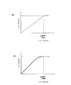
KGAINテーブル907は、前記外部環境入力手段の出力をKGAINに変換する変換手段である。KGAINは、例えば、図60(a)に示したように、暗い時は1を、明るいときは1.5を出力するようなテーブルであり、予め前記特性が記憶されているメモリで構成される。
【0598】
また、前記ユーザー入力手段の出力によって、ユーザーの好みに応じて、特性を、図60(a),(b),(c)等に選択することが可能である。この機能はKGAINテーブル907を構成する前記メモリの上位アドレスに前記ユーザー入力手段の出力を接続し、バンクを切り替えることによって実現する。
【0599】
(a)の特性は、外部環境が暗いときにKGAINを1、外部環境が明るいときにKGAINを1.5に変換する例である。
【0600】
この場合、後述するように外部環境が暗い時は、補正画像データDmultをオーバフロー無しに表示するためのゲインGを算出する。そして忠実に画像を表示できる。
【0601】
外部環境が明るい時は、ゲインGを大きめに算出し、表示輝度を大きくさせる。外部環境が明るい時は、補正画像データDmultは変調手段8をオーバフローするので、リミッタ905は乗算器904の出力(補正画像データDmult)をリミットしている。そのため輝度が大きくなる代わりに忠実度が悪くなる。
【0602】
このようなKGAINのテーブルを使うことによって、前述した主観評価(C.D.)で示したように、主観的に良好な表示が可能になった。
【0603】
(b)の特性は、外部環境が暗い時にKGAINを1、外部環境が明るい時にKGAINを2に変換する例である。この場合、(a)に比べ外部環境が明るい時のKGAINを大きくしたので、忠実度は悪くなるが(a)に比べ、より明るく画像を表示できる。ユーザーは、表示される入力画像の種類によって、ユーザー入力手段によって良好な変換テーブルを選択する。
【0604】
(c)の特性は、KGAINを1に固定にする例である。この場合、外部環境の明るさに係わらず、KGAINは1に設定するので補正画像データDmultをオーバフロー無しに表示することができる。入力画像に対して忠実に画像を表示したいときにユーザーは選択するとよい。
【0605】
さらに本発明者らは、検討を重ね、KGAINテーブル907は以下のような特性を持つことによっても、良好な結果を得ることがわかった。
【0606】
例えば、図61(d)に示すようにKGAIN=1の領域を低照度から中照度までとした例である。この場合外部環境がやや明るくとも忠実に画像を表示できる。また、図61(e)の様に外部照度に対してなめらかにKGAINを変化させた特性であると外部照度が変化した際にも、画像表示パネルを見る人にとって違和感が少ない。
【0607】
また、図62(f),(g)に示すようなカーブも有効であった。
【0608】
以上記述した特性をユーザー入力手段の出力によって選択できるようにすることによって、ユーザーの好み・入力画像等の種類によって良好に表示できる。
【0609】
以上のように本発明では、外部環境入力手段を設けることにより、外部環境情報(照度)を入力し、その値をKGAINに変換する変換手段(KGAINテーブル)を用いKGAINを得る。
【0610】
そしてゲイン算出手段より、ゲインGを算出し、算出されたゲインGを補正画像データあるいは入力画像データに乗じることによって、画像表示する場所の照度が基準値より低い時(暗い部屋で画面を見る時)、画面の輝度を大きくせず(すなわち明るく表示するより)前記走査配線の影響による画質劣化を正確に補正し、画像表示する場所の照度が基準値より高い時(明るい部屋で画面を見る時)、前記走査配線の影響による画質劣化を正確に補正することにより画面の輝度を大きくする(すなわち明るく表示する)ことによって、主観的に良好な表示画像を得ることができた。
【0611】
【発明の効果】
以上説明したように、本発明の画像表示装置によれば、従来からの課題であった、走査配線上の電圧降下による表示画像の劣化を好適に改善することができた。
【0612】
また、いくつかの近似を導入したことにより、電圧降下の影響を補正した、補正画像データを簡単に好適に計算することができ、非常に簡単なハードウエアでそれを実現することができるなど、非常に優れた効果があった。
【0613】
また、補正後の画像データが変調手段の入力範囲をオーバーフローしないように、オーバーフロー処理回路を備え、オーバーフロー処理においてはテレビジョン映像信号と、コンピュータ映像信号とで、オーバーフロー処理の方法を変えることにより高品位に画像を表示することができた。
【図面の簡単な説明】
【図1】本発明の実施の形態に係る画像表示装置の概観を示す図である。
【図2】表示パネルの電気的な接続を示す図である。
【図3】表面伝導型放出素子の特性を示す図である。
【図4】表示パネルの駆動方法を示す図である。
【図5】縮退モデルを説明する図である。
【図6】離散的に算出した電圧降下量を示すグラフである。
【図7】離散的に算出した放出電流の変化量を示すグラフである。
【図8】補正データの他の算出方法を説明するための図である。
【図9】画像データの大きさが192の場合の補正データの算出例を示す図である。
【図10】補正データの補間方法を説明するための図である。
【図11】第1の実施の形態に係る画像表示装置の概略構成を示すブロック図である。
【図12】画像表示装置の走査回路の構成を示すブロック図である。
【図13】画像表示装置の逆γ処理部の構成を示すブロック図である。
【図14】画像表示装置のデータ配列変換部の構成を示すブロック図である。
【図15】連続するフレームの例を示す図である。
【図16】連続するフレームでの画像データの大きさを示すグラフである。
【図17】連続するフレームでのゲインを示すグラフである。
【図18】画像表示装置の変調手段の構成及び動作を説明する図である。
【図19】画像表示装置の変調手段のタイミングチャートである。
【図20】画像表示装置の補正データ算出手段の構成を示すブロック図である。
【図21】画像表示装置の離散補正データ算出部の構成を示すブロック図である。
【図22】補正データ補間部の構成を示すブロック図である。
【図23】直線近似手段の構成を示すブロック図である。
【図24】画像表示装置のタイミングチャートである。
【図25】第2の実施の形態に係る画像表示装置の概略構成を示すブロック図である。
【図26】第3の実施の形態に係る画像表示装置の概略構成を示すブロック図である。
【図27】第4の実施の形態に係る画像表示装置の概略構成を示すブロック図である。
【図28】第5の実施の形態に係る画像表示装置の概略構成を示すブロック図である。
【図29】第5の実施の形態のゲイン算出部のブロック図である。
【図30】第6の実施の形態のゲイン算出部のブロック図である。
【図31】第8の実施の形態の画像表示装置の概略構成を示すブロック図である。
【図32】第8の実施の形態のフィルタ手段の構成を示すブロック図である。
【図33】第8の実施の形態のフィルタ手段の他の構成を示すブロック図である。
【図34】第8の実施の形態で説明した、ある動画像における最大補正画像データの変動を示す図である。
【図35】第8の実施の形態で説明した、フレーム番号対フィルタ手段の出力グラフである。
【図36】第8の実施の形態で説明した、フレーム番号対平均輝度(APL)グラフである。
【図37】第8の実施の形態で説明した、シーンチェンジを行ったフレーム番号対フィルタ手段の出力グラフである。
【図38】第9の実施の形態に係る画像表示装置の概略構成を示すブロック図である。
【図39】第10の実施の形態に係る画像表示装置の概略構成を示すブロック図である。
【図40】第10の実施の形態のフィルタ手段の構成を示すブロック図である。
【図41】第11の実施の形態で説明した、ノイズが乗った動画像の最大補正画像データの変化を示す図である。
【図42】第11の実施の形態に係る画像表示装置の概略構成を示すブロック図である。
【図43】第11の実施の形態の範囲選択手段の構成を示すブロック図である。
【図44】第11の実施の形態で説明した、ノイズ部を無視した時の最大補正画像データの変化を示す図である。
【図45】第11の実施の形態の範囲選択手段の他の構成を示すブロック図である。
【図46】第11の実施の形態の範囲選択手段の重みの特性を示す図である。
【図47】第12の実施の形態に係る画像表示装置の概略構成を示すブロック図である。
【図48】第13の実施の形態に係る画像表示装置の概略構成を示すブロック図である。
【図49】第14の実施の形態に係る画像表示装置の概略構成を示すブロック図である。
【図50】第15の実施の形態に係る画像表示装置の概略構成を示すブロック図である。
【図51】第15の実施の形態のゲイン制限部の第1の構成を示すブロック図である。
【図52】第15の実施の形態のゲイン制限部の第2の構成を示すブロック図である。
【図53】第15の実施の形態のゲイン制限テーブルのゲインの制限特性例である。
【図54】第16の実施の形態に係る画像表示装置の概略構成を示すブロック図である。
【図55】第16の実施の形態の特徴量算出手段の構成を示すブロック図である。
【図56】第16の実施の形態の判定手段の構成を示すブロック図である。
【図57】第16の実施の形態の特徴量算出手段の他の構成を示すブロック図である。
【図58】第17の実施の形態に係る画像表示装置の概略構成を示すブロック図である。
【図59】第17の実施の形態のリミッタ手段の特性を示す図である。
【図60】第17の実施の形態のKGAINテーブルの特性の一例を示す図である。
【図61】第17の実施の形態のKGAINテーブルの特性の一例を示す図である。
【図62】第17の実施の形態のKGAINテーブルの特性の一例を示す図である。
【図63】従来の画像表示装置の概略構成を示すブロック図である。
【符号の説明】
1 表示パネル
2 走査回路
3 同期分離回路
4 タイミング発生回路
5 シフトレジスタ
6 ラッチ
8 パルス幅変調手段
9 データ配列変換部
12 加算器
14 補正データ算出手段
14a 離散補正画像データ算出手段
14b 補正画像データ補間回路
17 逆γ処理部
19 遅延回路
20 最大値検出手段
21 ゲイン算出手段
22 乗算器
23 セレクタ
40 フィルタ手段
54 判定手段
60 特徴量算出手段
80 判定手段
100a,100b,100c,100d 点灯数カウント手段
101a,101b,101c,101d レジスタ
103 テーブルメモリ
107a,107b,107c コンパレータ
111 テーブルメモリ
123,124 デコーダ
400 範囲選択手段
409 デコーダ
901 最大値検出手段
902 ゲイン算出手段
903 ゲイン制限部
904 乗算器
905 リミッタ
906 外部環境入力手段
907 テーブル
908 ユーザー入力手段
1001 基板
1002 冷陰極素子
1003 行配線(走査配線)
1004 列配線(変調配線)
1007 フェースプレート
1008 蛍光膜
1009 メタルバック
9031 ゲイン制限レジスタ
9032 比較器
9033 スイッチ
9034 ゲイン制限テーブル[0001]
BACKGROUND OF THE INVENTION
The present invention relates to an image display apparatus including image forming elements arranged in a matrix, for example, a display including a plurality of surface conductive elements arranged in a matrix and a phosphor screen that emits light when irradiated with the electron beam. This is applied to a television receiver or a display device that receives a display signal from a television signal or a computer using a panel and displays an image, and in particular, a drive voltage caused by an electric resistance of a matrix wiring or the like of the display panel. The present invention relates to digital image data processing means having image data correcting means for correcting a voltage drop and amplitude adjusting means for controlling the amplitude of the corrected image data.
[0002]
[Prior art]
Conventionally, this type of image display device calculates the correction data by statistical calculation in order to correct the luminance drop due to the voltage drop due to the wiring resistance such as the electrical connection wiring to the electron-emitting device, and the electron beam Japanese Patent Laid-Open No. 8-248920 discloses an image display device having a configuration for combining a required value and a correction value.
[0003]
FIG. 63 is a schematic block diagram of an image display device according to the prior art. A configuration related to the correction of image data will be described below.
[0004]
First, luminance data for one line of the digital image signal is added by the
[0005]
On the other hand, the digital image signal is serial / parallel converted in the
[0006]
The
[0007]
Here, a statistical calculation process such as calculating the sum or average of the digital image signal is performed as in the summation process of luminance data for one line of the digital image signal in the
[0008]
On the other hand, as a general signal processing means, Japanese Patent Laid-Open No. 01-091515 discloses a pulse width modulation device having an overflow detector and a limiter, and Japanese Patent Laid-Open No. 07-273650 has an overflow detector and a gain controller. An A / D conversion circuit is disclosed.
[0009]
[Problems to be solved by the invention]
However, in the case of the prior art as described above, large-scale hardware such as a multiplier for each column wiring, a memory for outputting correction data, and a summer for giving an address signal to the memory is necessary. It was.
[0010]
Further, the correction may cause an overflow in the image data and disturb the display image.
[0011]
The present invention has been made to solve the above-mentioned problems of the prior art, and its object is to reduce the voltage drop due to the resistance of the matrix wiring of the display panel and the internal resistance of the scanning means with a small amount of hardware. An object of the present invention is to provide an image display device that corrects the influence appropriately and has excellent image quality.
[0012]
[Means for Solving the Problems]
In order to achieve the above object, the present invention provides:The following configuration is adopted. A plurality of row wirings and column wirings, a display panel connected to them and including image forming elements arranged on a matrix, scanning means for sequentially selecting and scanning the row wirings, and corresponding to input image data A corrected image data calculating unit that calculates corrected image data having a data value larger than the input image data value, an adjusting unit that adjusts the corrected image data or the value of the image data, and the column wiring. And a modulation unit that outputs a modulation signal to the column wiring, using the output from the adjustment unit as an input, and the adjustment unit corresponds to the whole or a part of the display area. A maximum value detection unit that detects a maximum value among the values of the correction image data, and a gain calculation unit that calculates a gain to be multiplied by the correction image data or the image data, The gain calculating unit calculates the gain so that a value obtained by smoothing the maximum value or a plurality of maximum values detected corresponding to a plurality of frames is within an input range of the modulation means. Image display device.
The corrected image data may be data for correcting the influence of a voltage drop generated by at least the resistance of the row wiring corresponding to the image data.
The corrected image data may be data obtained by performing correction on the image data to compensate for a decrease in luminance caused by a voltage drop due to a resistance of the row wiring.
It is preferable to have a limiter that limits the value of the adjusted corrected image data to be completely within the input range of the modulation means.
The gain may be an adaptive gain calculated for each frame.
The adjusting means includes a filter means for limiting the gain variation for each frame.
Good.
The adjustment unit further includes a scene switching determination unit that detects that the scene of the display image has changed, and the filter unit does not perform processing that restricts the variation in the gain when switching of the scene is determined. Is preferred.
The scene switching determination unit determines scene switching based on an inter-frame difference in average luminance level (APL) for each frame of input image data and / or a maximum inter-frame difference in corrected image data for each frame. Is preferred.
The adjustment unit preferably includes a gain limiting unit that limits the gain to a preset upper limit value or less.
It is preferable that the maximum value detection unit detects the maximum value of the corrected image data in a predetermined area, not the entire display area, of the corrected image data in the frame.
Preferably, the scene switching determination unit divides the display area into a plurality of areas, determines scene switching for each area, and determines scene switching for the entire screen from the determination result for each area. .
The adjustment unit includes an external illuminance input unit that detects illuminance around the image display device and outputs a signal corresponding to the detection result, and modulates the gain according to an output signal of the external illuminance input unit. Is preferred.
The adjustment means includes at least a first operation mode for outputting the adaptive gain calculated for each frame and a second operation mode for outputting a preset fixed gain that does not change for each frame, It is preferable to have two modes of operation.
The adjusting means selects the first operation mode when the input video signal is a television video signal, and the second adjustment unit selects the second operation mode when the input video signal is a computer video signal. It is preferable to select the operation mode.
A plurality of row wirings and column wirings, a display panel including image forming elements connected to them and arranged on a matrix, scanning means for sequentially selecting and scanning the row wirings, and modulation connected to the column wirings A correction image data calculation unit that calculates correction image data having a data value larger than the value of the input image data corresponding to the input image data, and the image display device comprising: So that the value of the corrected image data is within the input range of the modulating means. An adjustment unit that adjusts the correction image data or the value of the image data, and the modulation unit receives the output of the adjustment unit, outputs a modulation signal to the column wiring, and calculates the correction image data Means for calculating a voltage drop amount due to resistance of the row wiring at each of a discrete horizontal display position and a discrete time within one horizontal scanning period based on the input image data; Discrete corrected image data calculating means for calculating corrected image data corresponding to a discrete horizontal display position where the amount of voltage drop is calculated and a discrete time within one horizontal scanning period from the amount of voltage drop; An image display apparatus comprising: corrected image data interpolating means for interpolating the output of the corrected image data calculating means and calculating interpolated corrected image data.
The adjusting unit is configured to multiply the output of the discrete corrected image data calculating unit by a gain for adjusting a value, and so that the output of the corrected image data interpolating unit is within the input range of the modulating unit. It is preferable to have a limiter for limiting the value of the corrected image data.
The modulated signal is preferably a signal whose pulse width is modulated based on the image data.
The image forming element is preferably a surface conduction type emitting element.
[0021]
DETAILED DESCRIPTION OF THE INVENTION
A preferred embodiment of the present invention will be described below in detail with reference to the drawings, taking as an example an image display apparatus using a surface conduction electron-emitting device (hereinafter referred to as SCE).
[0022]
(First embodiment)
(Overview)
In a display device in which SCEs are arranged in a simple matrix, there is a phenomenon that a voltage drop occurs due to the current flowing into the scanning wiring and the wiring resistance of the scanning wiring, and the display image is deteriorated. Therefore, the image display apparatus according to the embodiment of the present invention is provided with a processing circuit that suitably corrects the influence of the voltage drop in the scanning wiring on the display image, and realizes it with a relatively small circuit scale. Configured.
[0023]
The correction circuit predicts and calculates the deterioration of the display image caused by the voltage drop according to the input image data, obtains correction data for correcting the deterioration, and corrects the input image data.
[0024]
As an image display device incorporating such a correction circuit, the present inventors have intensively studied an image display device of the following type.
[0025]
Hereinafter, in describing the present invention, first, an overview of a display panel of an image display device according to an embodiment of the present invention, electrical connection of the display panel, SCE characteristics, display panel driving method, and electrical resistance of scanning wiring The mechanism of the voltage drop caused by the above and the correction method and apparatus for the influence of the voltage drop will be described.
[0026]
(Overview of image display device)
FIG. 1 is a perspective view of a display panel used in the image display apparatus according to the present embodiment, and a part of the panel is cut away to show the internal structure. In the figure, 1005 is a rear plate, 1006 is a side wall, and 1007 is a face plate, and 1005 to 1007 form an airtight container for maintaining the inside of the display panel in a vacuum.
[0027]
A
[0028]
On the lower surface of the
[0029]
A metal back 1009 is formed on the lower surface of the
[0030]
Hv is a high-voltage terminal and is electrically connected to the metal back 1009. By applying a high voltage to the Hv terminal, a high voltage is applied between the
[0031]
(Characteristics of SCE)
The SCE has (emitter current Ie) vs. (element applied voltage Vf) characteristics and (element current If) vs. (element applied voltage Vf) characteristics as shown in FIG. Since the emission current Ie is remarkably smaller than the device current If and it is difficult to illustrate on the same scale, the two graphs are illustrated on different scales.
[0032]
The SCE has the following three characteristics with respect to the emission current Ie.
[0033]
First, when a voltage higher than a certain voltage (referred to as a threshold voltage Vth) is applied to the device, the emission current Ie increases rapidly. On the other hand, the emission current Ie is hardly detected at a voltage lower than the threshold voltage Vth.
[0034]
Second, since the emission current Ie changes depending on the voltage Vf applied to the element, the magnitude of the emission current Ie can be controlled by varying the voltage Vf.
[0035]
Third, since it has high-speed response, the emission time of the emission current Ie can be controlled by the application time of the voltage Vf.
[0036]
In the image display apparatus using the display panel shown in FIG. 1, if the first characteristic is used, it is possible to perform display by sequentially scanning the display screen. That is, a voltage equal to or higher than the threshold voltage Vth is appropriately applied to the driven element according to the desired light emission luminance, and a voltage lower than the threshold voltage Vth is applied to the non-selected element. By sequentially switching the elements to be driven, it is possible to perform display by sequentially scanning the display screen.
[0037]
Further, by utilizing the second characteristic, the light emission luminance of the phosphor can be controlled by the voltage Vf applied to the element, and image display can be performed.
[0038]
Further, by utilizing the third characteristic, the light emission time of the phosphor can be controlled by the time during which the voltage Vf is applied to the element, and an image can be displayed.
[0039]
In the image display device of the present invention, modulation is performed using the third characteristic.
[0040]
(Display panel drive method)
FIG. 4 shows an example of voltages applied to the voltage supply terminals of the scanning wiring and the modulation wiring when the display panel of the present invention is driven.
[0041]
Here, the horizontal scanning period I is a period during which the pixels in the i-th row emit light.
[0042]
In order to cause the pixels in the i-th row to emit light, the scanning wiring in the i-th row is set in a selected state, and the selection potential Vs is applied to the voltage supply terminal Dxi. Further, the voltage supply terminals Dxk (k = 1, 2,... N, where k ≠ i) of the other scanning wirings are set in a non-selected state, and a non-selection potential Vns is applied.
[0043]
In this embodiment, the selection potential Vs is set to -0.5 VSEL, which is half of the voltage VSEL shown in FIG. 3, and the non-selection potential Vns is set to the GND potential.
[0044]
A pulse width modulation signal having a voltage amplitude Vpwm was supplied to the voltage supply terminal of the modulation wiring. Conventionally, the pulse width of the pulse width modulation signal supplied to the j-th modulation wiring is determined according to the size of the image data of the pixel in the i-th row and j-th column of the image to be displayed unless correction is performed, A pulse width modulation signal corresponding to the size of image data of each pixel is supplied to all the modulation wirings.
[0045]
In the present invention, as will be described later, the pulse width of the pulse width modulation signal supplied to the j-th modulation wiring in order to correct the decrease in luminance due to the influence of the voltage drop is the i th of the image to be displayed. The pulse width modulation signal is supplied to all the modulation wirings according to the size of the image data of the pixel in the row and column j and the correction amount.
[0046]
In the present embodiment, the voltage Vpwm is set to +0.5 VSEL.
[0047]
(Voltage drop in scanning wiring)
As described above, the fundamental problem of the image display apparatus according to the present invention is that the voltage applied to the SCE decreases due to the potential on the scan line rising due to the voltage drop in the scan line of the display panel. The emission current from the SCE is reduced. Hereinafter, this voltage drop mechanism will be described.
[0048]
Although it depends on the design specifications and manufacturing method of the SCE, the element current for one element of the SCE is about several hundred μA when the voltage VSEL is applied.
[0049]
For this reason, when only one pixel on the selected scanning line is caused to emit light during a certain horizontal scanning period and the other pixels are not allowed to emit light, the element current flowing from the modulation wiring into the scanning wiring of the selected row is equivalent to one pixel. Since there is only a current (that is, the above-mentioned several hundreds of μA), a voltage drop hardly occurs and the light emission luminance does not decrease.
[0050]
However, when all the pixels in the selected row are caused to emit light in a certain horizontal scanning period, the current for all pixels flows from all the modulation wirings to the scanning wiring in the selected state. 100 mA to several A, and a voltage drop occurred on the scanning wiring due to the wiring resistance of the scanning wiring.
[0051]
If a voltage drop occurs on the scanning wiring, the voltage applied to both ends of the SCE is lowered. For this reason, the emission current emitted from the SCE is reduced, and as a result, the emission luminance is reduced.
[0052]
Further, more complicatedly, the magnitude of the voltage drop has a property of changing even during one horizontal scanning period by performing modulation by pulse width modulation.
[0053]
The case where the pulse width modulation signal supplied to each column outputs a pulse width modulation signal whose pulse width depends on the size of the data and whose rising edge is synchronized as shown in FIG. I'll think about it. In such a case, although depending on the input image data, in general, in one horizontal scanning period, the number of pixels that are lit increases as soon as the pulse rises, and then the pixels are turned off in order from the lower luminance. Therefore, the number of pixels to be lit decreases with time in one horizontal scanning period.
[0054]
Therefore, the magnitude of the voltage drop generated on the scanning wiring also tends to decrease gradually as the beginning of one horizontal scanning period.
[0055]
Since the output of the pulse width modulation signal changes every time corresponding to one gradation of modulation, the temporal change in voltage drop also changes every time corresponding to one gradation of the pulse width modulation signal.
[0056]
The voltage drop in the scanning wiring has been described above.
[0057]
(Voltage drop calculation method)
Next, a correction method for the influence of the voltage drop will be described in detail.
[0058]
In order to obtain the correction amount for reducing the influence of the voltage drop, as the first step, hardware for predicting the magnitude of the voltage drop and its time change in real time is required. As a display panel of an image display device, it is common to have thousands of modulation wirings, and it is very difficult to calculate the voltage drop at the intersection of all the modulation wirings and the scanning wiring. It is not realistic to create hardware that calculates the real time.
[0059]
Therefore, the voltage drop amount is calculated by blocking the position in the same row and also blocking the image data in the size direction.
[0060]
Such blocking is based on the following characteristics of the voltage drop.
[0061]
i) At a certain point in one horizontal scanning period, the voltage drop generated on the scanning wiring is a spatially continuous amount on the scanning wiring and is a very smooth curve.
[0062]
ii) Although the magnitude of the voltage drop varies depending on the display image, it changes with time corresponding to one gradation of pulse width modulation, and is roughly larger at the rising edge of the pulse, and gradually becomes smaller in time. Or keep its size.
[0063]
That is, in the driving method as shown in FIG. 4, the magnitude of the voltage drop does not increase within one horizontal scanning period.
[0064]
More specifically, the voltage change over time was roughly predicted by calculating the voltage drop based on the degenerate model described below for a plurality of times.
[0065]
(Calculation of voltage drop by degenerate model)
FIG. 5A is a diagram for explaining blocks and nodes when performing degeneration.
[0066]
In FIG. 5, only the selected scanning wiring, each modulation wiring, and the SCE connected to the intersection are shown for the sake of simplicity.
[0067]
Now, at a certain time in one horizontal scanning period, the lighting state of each pixel on the selected scanning wiring (that is, whether the output of the modulation means is “H” or “L”) is known. It shall be.
[0068]
In this lighting state, an element current flowing from each modulation wiring to the selected scanning wiring is defined as Ifi (i = 1, 2,... N, i is a column number).
[0069]
Also, as shown in FIG. 5, a block is defined with a group of n modulation wirings and a portion of the selected scanning wiring that intersects the SCEs arranged at the intersection. In this embodiment, the block is divided into four blocks.
[0070]
In addition, a position called a node is set at the boundary position of each block. The node is a horizontal position (reference point) for discretely calculating a voltage drop amount generated on the scanning wiring in the degenerate model.
[0071]
In the present embodiment, five nodes,
[0072]
FIG. 5B is a diagram for explaining a degenerate model.
[0073]
In the degeneration model, n modulation wirings included in one block in FIG. 5A are degenerated into one, and one degenerated modulation wiring is connected so as to be located at the center of the scanning wiring block. .
[0074]
Further, it is assumed that a current source is connected to the demodulated modulation wiring of each block, and the total current IF0 to IF3 in each block flows from each current source.
[0075]
That is, IFj (j = 0, 1,... 3) is
[Expression 1]
[0076]
In addition, the potential at both ends of the scan wiring is Vs in the example of FIG. 5A, whereas the GND potential in FIG. 5B flows into the scan wiring selected from the modulation wiring in the degenerate model. This is because the voltage drop amount of each part on the scanning wiring can be calculated by calculating the voltage (potential difference) of each part with the power supply part as a reference (GND) potential by modeling the current by the current source (that is, , Defined as a reference potential for calculating the voltage drop.)
[0077]
The SCE is omitted because, when viewed from the selected scanning wiring, if an equivalent current flows from the column wiring, the generated voltage drop itself does not change regardless of the presence or absence of the SCE. is there. Therefore, here, the SCE is omitted by setting the current value flowing from the current source of each block to the total current value (Equation 1) of the element currents in each block.
[0078]
In addition, the wiring resistance of the scanning wiring of each block is set to n times the wiring resistance r of the scanning wiring in one section (here, one section is the intersection of the scanning wiring with a certain column wiring and the adjacent column wiring. (In the present embodiment, the wiring resistance of the scanning wiring in one section is assumed to be uniform.)
[0079]
In such a degenerate model, the voltage drop amounts DV0 to DV4 generated at each node on the scanning wiring can be easily calculated by the following product-sum formula.
[0080]
[Expression 2]
[0081]
That is,
[Equation 3]
[0082]
However, aij is a voltage generated at the i-th node when a unit current is injected only into the j-th block in the degenerate model (hereinafter, this is defined as aij).
[0083]
The above aij is derived by Kirchhoff's law, and once calculated, it may be stored as a table.
[0084]
Furthermore, for the total current IF0 to IF3 of each block defined by
[Expression 4]
[0085]
However, in the above equation, “County” is a variable that takes 1 when the i-th pixel on the selected scanning line is in a lighting state, and takes 0 when it is in a light-off state.
[0086]
IFS is an amount obtained by multiplying the element current IF flowing when the voltage VSEL is applied to both ends of the SCE1 element by a coefficient α that takes a value between 0 and 1.
[0087]
That is,
[Equation 5]
[0088]
[0089]
Originally, in order to calculate the voltage drop amount, it is necessary to repeatedly calculate the voltage rise of the scanning wiring due to the voltage drop and the decrease amount of the element current due to this, but this convergence calculation is calculated by hardware. Is not realistic.
[0090]
Therefore, in the present invention, αIF is approximately used as the convergence value of IF.
[0091]
Specifically, the IF reduction rate (= α1) when the voltage drop amount is the maximum (when all white), and the IF reduction rate (= α2) when the voltage drop amount is (minimum = 0). ) Is estimated in advance, and is obtained as an average value of α1 and α2 or 0.8 × α1.
[0092]
FIG. 5C is an example of a result of calculating the voltage drop amounts DV0 to DV4 of each node using a degenerate model in a certain lighting state.
[0093]
Since the voltage drop becomes a very smooth curve, it is assumed that the voltage drop between the nodes approximately takes a value as shown by a dotted line in FIG.
[0094]
As described above, by using this degenerate model, it is possible to calculate the voltage drop at the node position at a desired point in time for the input image data.
[0095]
As described above, the voltage drop amount in a certain lighting state is simply calculated using the degenerate model.
[0096]
The voltage drop generated on the selected scanning wiring changes with time in one horizontal scanning period. As described above, this is the lighting state at that time for several times in one horizontal scanning period. And predicted by calculating the voltage drop for the lighting state using a degenerate model.
[0097]
Note that the number of lighting in each block at a certain point in one horizontal scanning period can be easily obtained by referring to the image data of each block.
[0098]
As an example, assume that the number of bits of input data to the pulse width modulation circuit is 8 bits, and the pulse width modulation circuit outputs a pulse width corresponding to the size of the input data.
[0099]
That is, when the input data is 0, the output is “L”, when the input data is 255, “H” is output during one horizontal scanning period, and when the input data is 128, the output is the first in one horizontal scanning period. It is assumed that “H” is output during the half period and “L” is output during the latter half period.
[0100]
In such a case, the number of lighting at the start time of the pulse width modulation signal (the rise time in the example of the modulation signal in this example) is simple if the number of input data to the pulse width modulation circuit is greater than 0. Can be detected.
[0101]
Similarly, the number of lighting at the center of one horizontal scanning period can be easily detected by counting the number of input data to the pulse width modulation circuit that is greater than 128.
[0102]
Thus, if the image data is compared with respect to a certain threshold and the number of outputs of the comparator being true is counted, the number of lightings at an arbitrary time can be easily calculated.
[0103]
Here, in order to simplify the following explanation, an amount of time called a time slot is defined.
[0104]
That is, the time slot represents the time from the rise of the pulse width modulation signal in one horizontal scanning period, and time slot = 0 is defined to represent the time immediately after the start time of the pulse width modulation signal. To do.
[0105]
Time slot = 64 is defined as representing the time when 64 gradations have elapsed from the start time of the pulse width modulation signal.
[0106]
Similarly, time slot = 128 is defined as representing the time when 128 gradations have elapsed from the start time of the pulse width modulation signal.
[0107]
In this example, the pulse width modulation is shown by using the rise time as a reference, and the pulse width is modulated from the rise time, but similarly, even when the pulse width is modulated using the pulse fall time as a reference, The direction in which the axis advances and the direction in which the time slot advances are opposite, but it goes without saying that the same applies.
[0108]
(Calculation of correction data from voltage drop)
As described above, the time change of the voltage drop during one horizontal scanning period can be calculated approximately and discretely by repeatedly calculating using the degenerate model.
[0109]
FIG. 6 is an example in which the voltage drop is repeatedly calculated for a certain image data, and the time change of the voltage drop in the scanning wiring is calculated (the voltage drop and the time change shown here are the same image). It is an example for the data, and the voltage drop for the other image data is naturally subject to other changes.)
[0110]
In FIG. 6, the voltage drop at each time is discretely calculated by performing the calculation by applying the degeneracy model to each of the four time points of time slots = 0, 64, 128, and 192.
[0111]
In FIG. 6, the amount of voltage drop at each node is connected by a dotted line, but the dotted line is shown for easy viewing of the figure. The voltage drop calculated by this degenerate model is □, ○, It was calculated discretely at the position of each node shown.
[0112]
The present inventors examined a method for calculating correction data for correcting image data from a voltage drop amount as the next stage in which the magnitude of the voltage drop and its time change can be calculated.
[0113]
FIG. 7 is a graph in which the emission current emitted from the SCE in the lighting state is estimated when the voltage drop shown in FIG. 6 occurs on the selected scanning wiring.
[0114]
The vertical axis represents the amount of emission current at each position in percentage with the magnitude of the emission current emitted when there is no voltage drop as 100%, and the horizontal axis represents the horizontal position.
[0115]
As shown in FIG. 7, at the horizontal position (reference point) of
The emission current when time slot = 0 is Ie0,
The emission current when time slot = 64 is Ie1,
The emission current at time slot = 128 is Ie2,
The emission current when the time slot is 192 is Ie3
And
[0116]
FIG. 7 is calculated from the voltage drop amount of FIG. 6 and the graph of “driving voltage versus emission current” of FIG. Specifically, the value of the emission current when a voltage obtained by subtracting the amount of voltage drop from the voltage VSEL is mechanically plotted.
[0117]
Accordingly, FIG. 7 merely means the current discharged from the SCE in the lit state, and the SCE in the unlit state does not release the current.
[0118]
Hereinafter, a method for calculating correction data for correcting image data from the voltage drop amount will be described below.
[0119]
(Correction data calculation method)
FIGS. 8A, 8B, and 8C are diagrams for explaining a method for calculating correction data of the voltage drop amount from the time change of the emission current of FIG. FIG. 8 shows an example in which correction data for image data having a size of 64 is calculated.
[0120]
The amount of light emission with brightness is nothing but the amount of emitted charge obtained by temporally integrating the emission current caused by the emission current pulse. Therefore, in the following, the description will be made based on the amount of emitted charges when considering the variation in luminance due to the voltage drop.
[0121]
If the emission current when there is no voltage drop effect is IE and the time corresponding to one gradation of pulse width modulation is Δt, it should be emitted by the emission current pulse when the image data is 64. The discharge charge amount Q0 is obtained by multiplying the amplitude IE of the discharge current pulse by the pulse width (64 × Δt),
[Formula 6]
[0122]
However, in practice, a phenomenon occurs in which the emission current decreases due to a voltage drop on the scanning wiring.
[0123]
The amount of charge emitted by the emission current pulse considering the influence of the voltage drop can be approximately calculated as follows. That is, if the emission currents at time slot = 0 and 64 of
[0124]
That is,
[Expression 7]
[0125]
Next, as shown in FIG. 8C, it is assumed that the influence of the voltage drop can be removed when the pulse width is increased by DC1 in order to correct the decrease in the emission current due to the voltage drop.
[0126]
Further, when the voltage drop is corrected and the pulse width is increased, the amount of emission current in each time slot is considered to change, but here, for simplicity, as shown in FIG. When = 0, the emission current is Ie0, and the emission current at time slot = (64 + DC1) is Ie1.
[0127]
Further, the emission current between the
[0128]
Then, the emission charge amount Q2 due to the emission current pulse after correction is
[Equation 8]
[0129]
If this is equal to the aforementioned Q0,
[Equation 9]
[0130]
Solving this for DC1,
[Expression 10]
[0131]
In this way, correction data when the image data is 64 was calculated.
[0132]
That is, the correction amount CDdata may be added to CDdata = DC1 as described in
[0133]
Similarly, for image data having a size of 192, correction amounts can be obtained for each of the three periods as shown in FIG.
[0134]
When the pulse width is 0, naturally, there is no influence of the voltage drop on the emission current, so that the correction data is 0 and the correction data CData added to the image data is also 0.
[0135]
In this way, the correction data is calculated for the discrete image data such as 0, 64, 128, and 192 in order to reduce the calculation amount.
[0136]
FIG. 10A shows an example of discrete correction data for certain input data obtained by this method.
[0137]
In the figure, the horizontal axis corresponds to the horizontal display position, and the position of each node is described. The vertical axis represents the size of the correction data.
[0138]
The discrete correction data is calculated with respect to the position of the node indicated by □, ○, ●, △ and the size of the image data Data (image data reference value = 0, 64, 128, 192). .
[0139]
(Interpolation method for discrete correction data)
The correction data calculated discretely is discrete with respect to the position of each node, and does not give correction data at an arbitrary horizontal position (column wiring number). At the same time, it is correction data for image data having a predetermined reference value size of image data at each node position, and does not give correction data according to the actual image data size. .
[0140]
Therefore, the inventors calculated correction data suitable for the size of the input image data in each column wiring by interpolating discretely calculated correction data.
[0141]
FIG. 10B is a diagram showing a method for calculating correction data corresponding to the image data Data at x located between the node n and the
[0142]
As a premise, it is assumed that the correction data has already been discretely calculated at the positions Xn and Xn + 1 of the nodes n and n + 1.
[0143]
Data that is input image data takes a value between Dk and Dk + 1 as image data reference values.
[0144]
Now, if the discrete correction data with respect to the reference value of the k-th image data at the node n is expressed as CDdata [k] [n], the correction data CA of the pulse width Dk at the position x is CDdata [k] [n]. And the value of CData [k] [n + 1] can be calculated as follows by linear approximation.
[0145]
That is,
## EQU11 ##
[0146]
However, Xn and Xn + 1 are the horizontal display positions of the nodes n and (n + 1), respectively, and are constants determined when determining the above-described block.
[0147]
Further, the correction data CB of the image data Dk + 1 at the position x can be calculated as follows.
[0148]
Ie
[Expression 12]
[0149]
By linearly approximating the correction data of CA and CB, the correction data CD for the image data Data at the position x can be calculated as follows.
[0150]
That is,
[Formula 13]
[0151]
As described above, in order to calculate the correction data suitable for the actual position and the size of the image data from the discrete correction data, it can be easily calculated by the methods described in
[0152]
If the correction data calculated in this way is added to the image data to correct the image data, and pulse width modulation is performed according to the corrected image data (referred to as corrected image data), it has been a conventional problem. The influence of the voltage drop in the display image can be reduced, and the image quality can be improved.
[0153]
In addition, the hardware for correction, which has been a problem for some time, can be reduced by introducing the approximation such as degeneration described so far, so the amount of calculation can be reduced. There was an excellent merit that it could be configured.
[0154]
(Explanation of functions of the entire system and each part)
Next, the hardware of an image display device incorporating correction data calculation means will be described.
[0155]
FIG. 11 is a block diagram showing an outline of the circuit configuration. In the figure, 1 is the display panel of FIG. 1, Dx1 to DxM and Dx1 ′ to DxM ′ are voltage supply terminals of the scanning wiring of the
[0156]
In FIG. 11, R, G, and B are RGB parallel input video data, Ra, Ga, and Ba are RGB parallel video data that has been subjected to inverse γ conversion processing, which will be described later, and Data is parallel / serial by the data
[0157]
(Synchronous separation circuit, selector)
The image display apparatus according to the present embodiment can display both television signals such as NTSC, PAL, SECAM, and HDTV, and VGA that is an output of a computer.
[0158]
The HDTV video signal is first separated into synchronization signals Vsync and Hsync by the
[0159]
A video signal output from a computer such as a VGA is A / D converted by an A / D converter (not shown) and supplied to the
[0160]
The
[0161]
(Timing generation circuit)
The
[0162]
The timing signal generated by the
[0163]
(Scanning circuit)
As shown in FIG. 12, the
[0164]
The
[0165]
Tscan is a timing signal group generated from a vertical synchronization signal, a horizontal synchronization signal, and the like.
[0166]
Each of the
[0167]
In order to reduce the voltage drop in the scanning wiring, the scanning circuit is preferably connected to both ends of the scanning wiring of the
[0168]
On the other hand, the embodiment of the present invention is effective even when the scanning circuit is not connected to both ends of the scanning wiring, and can be applied only by changing the parameters.
[0169]
(Reverse γ processing part)
The CRT has a light emission characteristic (hereinafter referred to as an inverse γ characteristic) of approximately 2.2 to the input.
[0170]
The input video signal considers such characteristics of the CRT, and is generally converted in accordance with a γ characteristic of the power of 0.45 so as to have a linear light emission characteristic when displayed on the CRT.
[0171]
On the other hand, when the display panel of the image display apparatus according to the embodiment of the present invention modulates according to the application time of the driving voltage, it has a light emission characteristic that is almost linear with respect to the application time, and therefore, the input video signal is converted to the inverse γ. It is necessary to perform conversion (hereinafter referred to as inverse γ conversion) based on the characteristics.
[0172]
The inverse
[0173]
The inverse
[0174]
The inverse
[0175]
(Data array converter)
The data
[0176]
Although not shown in FIG. 14, the FIFO memory is provided with two horizontal pixels of memory for odd lines and even lines. When odd-numbered video data is input, data is written to the odd-line FIFO, while image data stored in the previous horizontal scanning period is read from the even-line FIFO memory. When the even-numbered video data is input, the data is written in the even-line FIFO, while the image data stored in the previous horizontal period is read from the odd-line FIFO memory.
[0177]
The data read from the FIFO memory is parallel-serial converted by the selector according to the pixel arrangement of the display panel, and output as RGB serial image data SData. Although not described in detail, it operates based on a timing control signal from the
[0178]
(Delay circuit 19)
The image data SData rearranged by the data
[0179]
The
[0180]
(Adder 12)
The
[0181]
Note that the number of bits of the corrected image data Dout that is the output of the
[0182]
More specifically, it is assumed that the image data Data has a data width of 8 bits, the maximum value is 255, the correction data CD has a data width of 7 bits, and the maximum value is 120.
[0183]
At this time, the maximum value of the addition result was 255 + 120 = 375.
[0184]
On the other hand, the corrected image data Dout, which is the output of the
[0185]
(Overflow processing (amplitude adjustment means))
In the present invention, as described above, the correction is realized by the corrected image data Dout obtained by adding the calculated correction data CD to the image data Data.
[0186]
Now, it is assumed that the number of bits of the modulation means 8 is 8 bits and the number of bits of the corrected image data Dout that is the output of the
[0187]
Then, if the corrected image data Dout is directly connected to the input of the modulation means 8, overflow occurs.
[0188]
That is, since the data of 8 bits or more is folded and modulated by the modulation means for 8 bits, the image quality is remarkably lowered.
[0189]
Therefore, it is necessary to adjust the amplitude of the corrected image data before being input to the modulation means 8.
[0190]
If the number of input bits of the modulation means 8 is increased, overflow at the input of the modulation means 8 can be prevented, but on the other hand, the pulse width of the pulse output from the modulation signal cannot be extended to any extent.
[0191]
In other words, since the image display apparatus of the present invention performs driving by sequentially selecting scanning lines, the pulse width output from the modulation means 8 cannot extend the pulse beyond the assigned scanning time.
[0192]
Therefore, the upper limit of the input range of the modulation means 8 corresponds to the maximum input value determined by the number of bits of the modulation means 8 or the maximum pulse width (that is, the time for selecting one line of scanning wiring) that can be modulated. Defined by input data value.
[0193]
In the present embodiment, the upper limit of the input range of the modulation means 8 will be described below as an example when it is defined by the maximum value of the input data of the modulation means 8.
[0194]
As a configuration for preventing overflow, an all-white pattern having the maximum input image data ((R, G, B) = (FFh, FFh, FFh)) is input when the number of bits of the image data is 8 bits. At this time, the maximum value of the corrected image data Dout may be estimated in advance, and the corrected image data Dout may be multiplied by a gain such that the corrected image data Dout falls within the input range of the
[0195]
In the fixed gain method, overflow does not occur, but an image with a low average luminance can be displayed with a larger gain, but a small gain is multiplied, so the luminance of the display image may become darker. is there.
[0196]
On the other hand, the maximum value of the corrected image data Dout for each frame is detected, a gain is calculated so that the maximum value is within the input range of the modulation means 8, and the gain is multiplied by the corrected image data Dout to prevent overflow. May be. Hereinafter, this method is referred to as an adaptive gain method.
[0197]
In the adaptive gain method, the maximum value detecting means 20 for detecting the maximum value MAX for each frame of the corrected image data Dout and the gain calculation for calculating the gain G1 for multiplying the corrected image data Dout from the maximum value. Means 21 and a multiplier for multiplying the corrected image data Dout and the gain G1 are necessary.
[0198]
In the adaptive gain method, the gain for preventing overflow is preferably calculated in units of frames.
[0199]
For example, it is possible to prevent the overflow by calculating the gain for each horizontal line. However, in this case, the display image is uncomfortable due to the difference in gain for each horizontal line, which is not preferable.
[0200]
The outline of the fixed gain method and the adaptive gain method has been described above.
[0201]
The present inventors have confirmed that the amplitude of the corrected image data can be suitably adjusted regardless of which method is used to calculate the gain.
[0202]
Therefore, in the present embodiment, amplitude adjustment is performed by the adaptive gain method.
[0203]
Hereinafter, in the present embodiment, a circuit configuration as means for adjusting the amplitude of the corrected image data by the adaptive gain method will be described in detail.
[0204]
(Maximum value detection means (maximum value detection unit))
The maximum value detecting means 20 of the present invention is connected to each part as shown in FIG.
[0205]
The maximum
[0206]
The maximum value detection means 20 is a circuit that can be easily configured by a comparator and a register. The maximum
[0207]
If the value of the register is cleared to 0 at the beginning of the frame, the maximum value of the corrected image data in the frame is stored in the register at the end of the frame.
[0208]
The maximum value of the corrected image data Dout detected in this way is transferred to the gain calculating means 21.
[0209]
(Gain calculation means (gain calculation unit))
The gain calculating means 21 is a means for calculating a gain for performing amplitude adjustment so that the corrected image data Dout is within the input range of the modulating means 8 based on the adaptive gain method.
[0210]
As for the gain, when the maximum value detected by the maximum
[Expression 14]
[0211]
The gain calculation means 21 updates the gain in the vertical blanking period and changes the gain value for each frame.
[0212]
In the configuration of the image display device of the present invention, the gain multiplied by the corrected image data of the current frame is calculated using the maximum value of the corrected image data of the previous frame.
[0213]
Therefore, strictly speaking, overflow may occur due to a difference in corrected image data for each frame.
[0214]
For such a problem, it is preferable to provide a limiter means to be described later for the output of the multiplier that multiplies the corrected image data and the gain, and to design the circuit so that the output of the multiplier falls within the input range of the modulation means. It was. It can be considered that the above overflow processing is performed using the correlation of the corrected image data (image data) between adjacent frames.
[0215]
If a frame memory is provided between the maximum value detection circuit and the multiplier, an overflow can be prevented with a configuration without a time delay.
[0216]
In addition, the present inventors have confirmed that the gain determination method of the adaptive gain method may calculate the gain by the following method.
[0217]
That is, as the gain to be applied to the corrected image data of the current frame, the maximum value of the corrected image data detected in the frame before the current frame is smoothed (averaged) in the frame direction, and the average value AMAX is obtained. On the other hand, the gain G1 ′ is
[Expression 15]
[0218]
In the third method, the gain G1 for each frame may be calculated by
[0219]
The present inventors have confirmed that any of these three methods is preferable. On the other hand, the second and third methods are more likely to flicker in the display image than the first method. There is another effect that is greatly reduced, which is very suitable (this will be described later with reference to FIGS. 15 to 17).
[0220]
The present inventors have examined the number of frames to be averaged with respect to the second method and the third method. For example, when 16 frames to 64 frames are averaged, a preferable image with less flicker is obtained. Obtained.
[0221]
Even in the case of the second and third methods, there is a correlation between frames in the (corrected) image data as in the first method, so that the probability of occurrence of overflow can be reduced. Overflow cannot be prevented.
[0222]
As a countermeasure for this, it was further preferable that the overflow was generally prevented by the above-described method, and a limiter was provided at the output of the multiplier to completely prevent the overflow.
[0223]
FIG. 15 is a diagram for explaining flicker by taking the first method and the second method as examples.
[0224]
FIG. 15 is an example of a moving image in which a white bar rotates counterclockwise in a gray background. When such an image is displayed, the size of the correction data CD changes for each frame as the bar rotates.
[0225]
FIG. 16 is a diagram for explaining corrected image data when such a moving image is corrected. In FIG. 16, the corrected image data having the maximum value in each frame is extracted and graphed.
[0226]
Note that the white portion in FIG. 16 corresponds to the original image data, and the gray portion corresponds to the portion expanded by performing the correction.
[0227]
When an image as shown in FIG. 15 is displayed, the maximum value of the corrected image data of consecutive frames varies as shown in FIG.
[0228]
Therefore, when the gain is set for each frame as shown in
[0229]
On the other hand, when the gain is determined by Expression 13, since the gain is averaged, as shown in FIG. 17B, the fluctuation of the gain is reduced and the fluctuation of the luminance is reduced, so that the flicker feeling is reduced. There was an excellent effect.
[0230]
In FIG. 17B, the white circle graph represents the gain according to
[0231]
Although the third method has not been discussed in detail here, the present inventors have confirmed that the flicker is reduced because the gain variation is reduced as in the second method.
[0232]
The gain calculation means 21 averages the gain for the continuous scene screen as described above. On the other hand, when the image scene changes, the gain calculation means 21 uses the gain after the scene change. It was preferred to change quickly.
[0233]
On the other hand, the gain calculating means 21 is provided with a preset threshold value, which is a scene switching threshold value Gth, and the gain of the previous frame calculated by
[Expression 16]
[Expression 17]
[0234]
Especially as the values of A and B,
A = 1, B = 1/16 to 1/64
It was preferable when we set to degree.
[0235]
The scene switching determination and the gain calculation method are not limited to this, and may be detected by a configuration as shown in an eighth embodiment described later.
[0236]
(Multiplier)
The gain G1 calculated by the gain calculating means 21 and the corrected image data Dout that is the output of the
[0237]
(Limiter means (limitation means))
As described above, there is no problem if the gain can be determined so that overflow does not occur, but according to some of the gain determination methods described above, it is difficult to determine the gain so that overflow does not occur. A limiter can also be provided.
[0238]
The limiter has a preset limit value. The limit value is compared with the output data Dmul input to the limiter. If the limit value is smaller than the output data, the limit value is output and the limit value is greater than the output data. Is larger, output data is output (the signal name in FIG. 11 is the corrected image data Dlim).
[0239]
The corrected image data Dlim completely limited to the input range of the modulation means 8 by the limiter means is supplied to the modulation means 8 via a shift register and a latch.
[0240]
(Shift register, latch circuit)
The corrected image data Dlim, which is the output of the limiter circuit, is serial / parallel converted from the serial data format to the parallel image data ID1 to IDN for each modulation wiring by the
[0241]
In this embodiment, the image data ID1 to IDN and D1 to DN are each 8-bit image data. These operation timings operate based on the timing control signals TSFT and Dataload from the timing generation circuit 4 (FIG. 11).
[0242]
(Details of modulation means)
Parallel image data D <b> 1 to DN as outputs of the
[0243]
As shown in FIG. 18A, the modulation means 8 is a pulse width modulation circuit (PWM circuit) including a PWM counter and a comparator and a switch (FET in the figure) for each modulation wiring.
[0244]
The relationship between the image data D1 to DN and the output pulse width of the modulation means is linear as shown in FIG.
[0245]
FIG. 18C shows three examples of the output waveform of the modulation means.
[0246]
In FIG. 18C, the upper waveform is the waveform when the input data to the modulation means is 0, the middle waveform is the waveform when the input data to the modulation means is 128, and the lower waveform is the modulation waveform. It is a waveform when the input data to the means is 255.
[0247]
In this example, the number of bits of input data D1 to DN to the modulation means is 8 bits.
[0248]
In the above description, there is a place where a modulation signal having a pulse width corresponding to one horizontal scanning period is output when the input data of the modulation means is 255. For details, FIG. As described above, although there is a very short time before the pulse rises and after the fall, there are a few periods during which the pulses are not driven to provide a timing margin.
[0249]
FIG. 19 is a timing chart showing the operation of the modulating means of the present invention.
[0250]
In FIG. 19, Hsync is a horizontal synchronizing signal, Dataload is a load signal to the
[0251]
As shown in FIG. 19, when one horizontal scanning period starts, the
[0252]
As shown in the figure, the PWM counter starts counting based on Pwmstart and Pwmclk. When the count value reaches 255, the counter is stopped and the
[0253]
The comparator provided for each column compares the count value of the PWM counter with the image data of each column, and outputs High when the value of the PWM counter is equal to or greater than the image data, and outputs Low during other periods. .
[0254]
The output of the comparator is connected to the gate of the switch in each column. During the period when the output of the comparator is Low, the upper switch (Vpwm side) in the figure is ON, and the lower switch (GND side) is OFF. The modulation wiring is connected to the voltage Vpwm.
[0255]
On the contrary, during the period when the output of the comparator is High, the upper switch in the figure is turned OFF, the lower switch is turned ON, and the voltage of the modulation wiring is connected to the GND potential.
[0256]
As each unit operates as described above, the pulse width modulation signal output from the modulation means has a waveform in which the rising edges of the pulses are synchronized as shown by D1, D2, and DN in FIG.
[0257]
(Correction data calculation means)
The correction data calculation means 14 is a circuit that calculates correction data for the voltage drop by the correction data calculation method described above. As shown in FIG. 20, the correction data calculation means 14 includes two blocks, a discrete correction data calculation unit and a correction data interpolation unit.
[0258]
The discrete correction data calculation unit calculates a voltage drop amount from the input video signal, and calculates correction data discretely from the voltage drop amount. The discrete correction data calculation unit calculates the correction data discretely by introducing the concept of the above-described degeneration model in order to reduce the calculation amount and the hardware amount.
[0259]
The correction data calculated discretely is interpolated by a correction data interpolation unit, and correction data CD suitable for the size of the image data and the horizontal display position x is calculated.
[0260]
(Discrete correction data calculation unit)
FIG. 21 shows a discrete correction data calculation unit for calculating correction data discretely according to the present invention.
[0261]
As described below, the discrete correction data calculation unit divides the image data into blocks, calculates the statistic (number of lightings) for each block, and calculates the time change of the voltage drop at each node position from the statistic. A function as a voltage drop amount calculation unit to calculate, a function to convert the voltage drop amount for each time into a light emission luminance amount, a function to calculate the light emission luminance total amount by integrating the light emission luminance amount in the time direction, and those To correction data for a reference value of image data at discrete reference points.
[0262]
In FIG. 21, 100a to 100d are lighting number counting means, 101a to 101d are register groups for storing the number of lighting at each time for each block, 102 is a CPU, 103 is a parameter aij described in
[0263]
The lighting number counting means 100a to 100d are composed of a comparator and an adder as shown in FIG. The video signals Ra, Ga, Ba are respectively input to the
[0264]
Cval corresponds to the image data reference value set for the image data described above.
[0265]
The
[0266]
The outputs of the comparators are added to each other by the
[0267]
0, 64, 128, and 192 are input to the lighting number counting means 100a to 100d as comparison values Cval of the comparators, respectively.
[0268]
As a result, the lighting number counting means 100a counts the number of image data larger than 0 among the image data, and stores the total for each block in the
[0269]
Similarly, the lighting number counting means 100b counts the number of image data larger than 64 of the image data, and stores the total for each block in the
[0270]
Similarly, the lighting number counting means 100c counts the number of image data larger than 128 among the image data, and stores the total for each block in the
[0271]
Similarly, the lighting number counting means 100d counts the number of image data larger than 192 in the image data, and stores the total for each block in the register 101d.
[0272]
When the number of lightings for each block and time is counted, the CPU reads the parameter table aij stored in the
[0273]
In this embodiment, a product-sum operation function for smoothly performing the calculation of
[0274]
As a means for realizing the calculation shown in
[0275]
That is, the number of lighting of each block may be input, and the voltage drop amount at each node position may be stored in the memory for all possible input patterns.
[0276]
When the calculation of the voltage drop amount is completed, the CPU reads the voltage drop amount for each block for each time from the
[0277]
The calculated discrete correction data was stored in the
[0278]
(Correction data interpolation unit)
The correction data interpolation unit is a means for calculating correction data corresponding to the position (horizontal position) where the image data is displayed and the size of the image data. The means interpolates discretely calculated correction data, thereby calculating correction data corresponding to the display position (horizontal position) of the image data and the size of the image data.
[0279]
FIG. 22 is a diagram for explaining the correction data interpolation unit.
[0280]
In FIG. 22, a
[0281]
Further, the
[0282]
Further, the straight line approximation means 120 to 122 are straight line approximation means a to c for performing straight line approximation of
[0283]
FIG. 23 shows a configuration example of the linear approximation means a. In general, the linear approximation means can be constituted by a subtractor, an integrator, an adder, a divider, etc., as represented by the operators of
[0284]
However, preferably, the number of column wirings between nodes for calculating discrete correction data and the interval between image data reference values for calculating discrete correction data (that is, the time interval for calculating a voltage drop) are a power of 2. This configuration has the advantage that the hardware can be configured very easily. If they are set to a power of 2, in the divider shown in FIG. 23, Xn + 1−Xn becomes a power of 2 and may be bit-shifted.
[0285]
If the value of Xn + 1−Xn is always a constant value and is a value represented by a power of 2, the addition result of the adder may be shifted by the power of the power and output. There is no need to make it.
[0286]
Further, by setting the interval between the nodes for calculating the discrete correction data and the interval between the image data to powers of 2 at other locations, for example, the
[0287]
(Operation timing of each part)
FIG. 24 shows a timing chart of the operation timing of each part.
[0288]
In FIG. 24, Hsync is a horizontal synchronization signal, DotCLK is a clock generated from the horizontal synchronization signal Hsync by a PLL circuit in the timing generation circuit, R, G, and B are digital image data from the input switching circuit, and Data is a data array. The converted image data, Dlim is the output of the limiter means, the corrected image data subjected to the voltage drop correction, TSFT is the shift clock for transferring the corrected image data Dlim to the
[0289]
With the start of one horizontal period, the digital image data RGB is transferred from the
[0290]
R_I, G_I, and B_I are input to the correction
[0291]
Following the calculation of the voltage drop amount, discrete correction data is calculated, and the calculation result is stored in the register.
[0292]
In the scanning period I + 1, the correction data interpolating means interpolates the discrete correction data and calculates the correction data in synchronization with the output of the image data Data_I one horizontal scanning period before from the data array conversion unit. The interpolated correction data is supplied to the
[0293]
The
[0294]
The pulse width modulation means 8 outputs a pulse width modulation signal having a pulse width corresponding to the latched image data. In the image display apparatus according to the present embodiment, as a result, the pulse width output from the modulation unit is displayed with a distance of two horizontal scanning periods with respect to the input image data.
[0295]
When an image is displayed using such an image display device, it is possible to correct the amount of voltage drop in the scanning wiring, which has been a problem in the past, and to improve the deterioration of the display image caused by that. A good image could be displayed.
[0296]
In addition, by introducing several approximations, the correction amount of image data for correcting the voltage drop can be easily and suitably calculated, and can be realized with very simple hardware. And so on.
[0297]
(Second Embodiment)
In the first embodiment, the maximum value of the corrected image data is detected, the gain is calculated so that the maximum value corresponds to the maximum value of the input range of the modulation means, and the gain and the corrected image data are multiplied. And overflow was prevented.
[0298]
In contrast, in the second embodiment, the maximum value of the corrected image data is detected in the same manner, but before correction is performed so that the maximum value corresponds to the maximum value of the input range of the modulation means. The size of the image data is limited.
[0299]
In other words, in order to prevent overflow, the input image data is multiplied by a gain to reduce the amplitude range, thereby preventing overflow.
[0300]
Hereinafter, the overflow processing according to the present embodiment will be described with reference to FIG.
[0301]
In FIG. 25, 22R, 22G, and 22B are multipliers, 9 is a data array conversion unit, 5 is a shift register for one line of image data, 6 is a latch circuit for one line of image data, and 8 is modulated to a modulation wiring of the display panel. Pulse width modulation means for outputting a signal, 12 is an adder, 14 is correction data calculation means, 20 is a maximum value detection circuit (means) for detecting the maximum value of the corrected image data Dout in the frame, and 21 is a gain calculation. Means.
[0302]
Also, R, G, and B are RGB parallel input video data, Ra, Ga, and Ba are RGB parallel video data that has been subjected to inverse γ conversion, and Rx, Gx, and Bx are multiplied by a gain G2 by a multiplier. Image data, gain G2 is the gain calculated by the gain calculation unit, Data is image data that has been parallel-serial converted by the data
[0303]
(
[0304]
More specifically, the multiplier multiplies the image data by the gain G2 in accordance with the gain determined by the gain calculation means 21, and outputs the multiplied image data Rx, Gx, Bx.
[0305]
The gain G2 is a value calculated by the gain calculation means 21 so that corrected image data Dout, which is the result of adding image data Data and correction data CD in an
[0306]
(Maximum value detection means (maximum value detection unit))
Next, the maximum value detection means 20 will be described.
[0307]
The maximum value detection means 20 of the present invention is connected to each part as shown in FIG.
[0308]
The maximum
[0309]
(Gain calculation means (gain calculation unit))
The
[0310]
On the other hand, as another method of calculating the gain, the gain may be calculated by the fixed gain method in the configuration of the present embodiment (FIG. 25).
[0311]
The gain determination method is as follows. The maximum value of the corrected image data Dout in one frame is MAX, the maximum value of the input range of the modulation means is INMAX, and the gain G2 calculated by the gain calculation means for the previous frame is GB.
[Expression 18]
[0312]
In the gain calculation means 21, the gain is updated in the vertical blanking period, and the gain value is changed for each frame.
[0313]
Note that the configuration of the image display apparatus according to the present embodiment is configured to calculate the gain by which the corrected image data of the current frame is multiplied using the maximum value of the corrected image data of the previous frame (that is, (It is configured to prevent overflow using the correlation of corrected image data (image data) between frames.)
[0314]
Therefore, strictly speaking, overflow may occur due to a difference in corrected image data for each frame.
[0315]
To solve this problem, it is more preferable to provide a limiter means for the output of the multiplier that multiplies the corrected image data and the gain, and to design the circuit so that the output of the multiplier always falls within the input range of the modulation means. won.
[0316]
In addition, as in the first embodiment, the inventors set the maximum value of the corrected image data detected in a frame earlier than the current frame in order to obtain another effect of preventing flicker. Average, and for the average value AMAX,
[Equation 19]
[0317]
As another method, the gain G2 for each frame may be calculated by
[0318]
The present inventors have confirmed that any of these three methods is preferable in terms of preventing overflow, but considering that flicker occurs as described in the first embodiment. For example, it is preferable to calculate by averaging.
[0319]
The present inventors examined the number of frames for averaging the maximum value of the corrected image data in the gain calculation method of Expression 15, but the maximum of the corrected image data from 16 to 64 frames before the current frame is examined. When the values were averaged, it was favorable.
[0320]
In this method, as shown in FIG. 25, it is needless to say that it is preferable to provide a limiter for limiting the output of the adder to completely prevent overflow.
[0321]
Further, as in the first embodiment, a scene change may be detected to change the gain calculation method.
[0322]
(Third embodiment)
In the first embodiment, a reference value of discrete image data is set for input image data, a reference point is set on the row wiring, and the size of the image data reference value at the reference point is set. Correction data for image data was calculated.
[0323]
Furthermore, the correction data calculated according to the horizontal display position of the input image data and its size is calculated by interpolating the correction data calculated discretely, and corrected by adding the image data with an adder. Was realized.
[0324]
On the other hand, the same correction can be performed by the configuration of FIG. The third embodiment will be described below with reference to FIG.
[0325]
26 differs from FIG. 11 in that 14 correction data calculation means and
[0326]
The flow for calculating the corrected image data of the image display device of FIG. 26 will be described below.
[0327]
(1) Discrete corrected image data CDA (that is, a correction result that is the sum of the discrete correction data and the image data reference value) for the discrete horizontal position and the image data reference value is calculated (discrete corrected image data calculation unit ).
[0328]
(2) The corrected image data calculated discretely is interpolated, and corrected image data corresponding to the size of the input image data Data and the horizontal display position x is calculated (corrected image data interpolation circuit).
[0329]
(3) The maximum value of the interpolated corrected image data is detected (maximum value detection means), and the gain G1 is calculated (gain calculation means) so that it is within the input range of the modulation means. The calculated gain G1 is multiplied by the corrected image data Dout (multiplier), and the amplitude of the corrected image data is completely limited by a limiter, which is input to the shift register, latch, and modulation means.
[0330]
Note that the calculation method of the discrete correction image data CDA described in (1) can be easily calculated by modifying the conventional method of calculating the discrete correction data (
[0331]
That is,
[0332]
In such a configuration, since the corrected image data obtained by adding the image data and the correction data is calculated at the discrete calculation stage, it is not necessary to add the image data and the correction data after the interpolation. For this reason, the
[0333]
Further, the configuration of the corrected image data interpolation circuit can be configured with the same configuration as that of the correction data interpolation unit of FIG. 22 described in the first embodiment.
[0334]
As described above, even with such a configuration, the influence of the voltage drop can be suitably corrected, which is very preferable.
[0335]
In the present embodiment, the configuration for preventing overflow of the corrected image data is the configuration of the first embodiment. However, the configuration of the second embodiment is not particularly limited thereto. Needless to say, the configuration may be adopted.
[0336]
(Fourth embodiment)
In the third embodiment, a reference value of discrete image data is set for input image data, a reference point is set on the row wiring, and image data of the size of the image data reference value at the reference point is set. The corrected image data for is calculated.
[0337]
Further, the corrected image data corresponding to the horizontal display position and the size of the input image data is calculated by interpolating the corrected image data calculated discretely.
[0338]
Further, by multiplying the calculated corrected image data Dout by a gain, the amplitude of the corrected image data Dout is adjusted and adjusted so as to correspond to the input range of the modulation means.
[0339]
Furthermore, the gain is calculated according to
[0340]
Further, the gain was calculated according to Equation 15 for another purpose of preventing flicker.
[0341]
On the other hand, the same effect can be obtained by the configuration of FIG. The fourth embodiment will be described below with reference to FIG.
[0342]
27 differs from FIG. 26 in that the discrete correction image data CDA is multiplied by the gain value calculated by the gain calculation means 21. In FIG.
[0343]
By multiplying the gain, the amplitude of the discrete corrected image data CDA is adjusted and output to the corrected image
[0344]
The corrected image
[0345]
At this time, the amplitude adjustment is performed so that the output Dout of the corrected image
[0346]
However, strictly speaking, the gain G3 when multiplying the discrete corrected image data is
[Expression 20]
[Expression 21]
[0347]
However,
INMAX: Maximum value of the input range of the modulation means
MAX: Maximum value of the corrected image data Dout for each frame
AMAX: A value obtained by averaging the maximum value MAX for each frame
GB: Gain G3 calculated by the gain calculation means in the previous frame
It is.
[0348]
Therefore, in the above configuration, the frequency of occurrence of overflow can be greatly reduced, but strictly speaking, overflow cannot be completely prevented.
[0349]
Therefore, also in the present embodiment, by providing a limiter between the corrected image
[0350]
The position where the limiter is provided may be the position shown in FIG. 27, but is not particularly limited thereto.
[0351]
For example, the same effect can be obtained by providing another limiter for limiting the discrete corrected image data CDL to be within the input range of the modulation means without providing the limiter shown in FIG.
[0352]
(Fifth embodiment)
In the first embodiment, the fixed gain method and the adaptive gain method have been described as the method for determining the gain.
[0353]
The adaptive gain method is a method of detecting the maximum value of the corrected image data for each frame and adaptively calculating the gain so that it does not overflow.
[0354]
The adaptive gain method has the advantage that the display image can be brightened compared to the fixed gain method because the range is adaptively adjusted for both bright and dark images. Variations in luminance may be observed due to variations in gain.
[0355]
Therefore, the inventors further studied, and as a result, the luminance fluctuation due to the gain fluctuation is not so noticeable when the television video is displayed, but when the video output from the computer is displayed. I ’ve found that I ’m very worried.
[0356]
For example, consider a window screen that is often seen in video output by a computer.
[0357]
As an example, when a white window (R, G, B) = (FFh, FFh, FFh) is displayed on the background of green (8 bits (R, G, B) = (0, FFh, 0)) Consider display pattern 1).
[0358]
In this case, the portion where the corrected image data is maximized in the frame is a portion displaying a white window.
[0359]
On the other hand, when the white window is closed to have only a green background (hereinafter referred to as display pattern 2), the maximum value of the corrected image data is determined by the green background.
[0360]
In the image display device of the present invention, the maximum value of the corrected image data is larger in the
“Gain of
It becomes.
[0361]
Then, when the
[0362]
When switching from
[0363]
Such a sense of incongruity due to fluctuations in brightness can be made inconspicuous by the process of averaging the gains described above, but it is extremely difficult for video signals that are flat in the screen, such as computer video signals. However, since the luminance fluctuates, it is not so preferable.
[0364]
Therefore, the present inventors calculated the gain by the fixed gain method when displaying the video signal of the computer, and calculated the gain by the adaptive gain method when displaying the television signal. I liked it very much.
[0365]
FIG. 28 is a diagram showing an image display apparatus according to the present embodiment.
[0366]
In FIG. 28, the difference from the entire system diagram of the first embodiment (FIG. 11) is that the type signal SVS of the video signal selected from the
[0367]
Thereby, the gain calculating means 21 calculates the gain by the fixed gain method when the video signal to be displayed is the video output of the computer, and calculates the gain G1 by the adaptive gain method when it is a television image. did.
[0368]
FIG. 29 is a diagram for explaining the gain calculating means 21 of the present embodiment.
[0369]
In the gain calculation means 21, the gain is calculated by an adaptive gain method using an adaptive gain calculation circuit based on the maximum value of the corrected image data detected by the maximum value detection means 20. The calculated gain GD is supplied to the selector.
[0370]
The gain GS of the fixed gain method is also supplied to the selector.
[0371]
The selector refers to the video type signal SVS, and when the video signal to be displayed is a television signal, the output G1 of the selector is selected as the gain GD by the adaptive gain method and is a computer video signal The gain GS of the fixed gain method is selected.
[0372]
In the present embodiment, the fixed gain method is used when displaying a computer video signal, and the adaptive gain method is used when displaying a television video signal. The user may select which mode to set in accordance with the interface.
[0373]
Further, a video input terminal for a computer and a video input terminal for a television may be provided, and the mode switching may be automatically performed based on which is the currently displayed video.
[0374]
As a mode for selecting the display quality of the image display device, select the adaptive gain method when you want to display a bright screen with priority on peak luminance, and select a fixed gain when you want to prioritize screen fidelity over peak luminance. You may choose the law.
[0375]
As described above, when a television video signal is displayed, the gain is calculated by the adaptive gain method, and when a computer video signal is displayed, the gain is calculated by the fixed gain method. While displaying a bright screen, it was possible to display a preferable image without a sense of incongruity when displaying a video signal from a computer.
[0376]
In the present embodiment, as shown in FIG. 28, the configuration of the first embodiment is adopted as the configuration for preventing the overflow of the corrected image data. However, the configuration is particularly limited to this. There is no.
[0377]
That is, the same effect can be obtained even in the configuration for adjusting the amplitude range of the input image data shown in the second embodiment (FIG. 25).
[0378]
In addition, similar effects can be obtained even when the amplitude range of the discrete corrected image data is adjusted as in the fourth embodiment (FIG. 27).
[0379]
(Sixth embodiment)
In the fifth embodiment, the gain is determined by the fixed gain method when displaying the computer video signal, and the gain is determined by the adaptive gain method when displaying the television video signal (FIG. 29).
[0380]
In the sixth embodiment, when the
[0381]
In FIG. 30A, the adaptive gain calculation circuit calculates the adaptive gain GD with reference to the maximum value MAX of the corrected image data from the maximum value detection means 20. The calculated gain GD is input to the limiter.
[0382]
The limiter is a circuit that limits the gain GD in accordance with the limit value output from the limiter register and outputs it as the gain G1.
[0383]
The limiter register stores a plurality of limit values.
[0384]
Which of the plurality of limit values is output is determined by the video type signal SVS and the dynamic mode / low power mode switching signal SMODE shown in FIG.
[0385]
In the present embodiment, the relationship between a plurality of limiter values is set as follows, which is preferable.
[0386]
Dynamic mode> Low power mode> Computer mode
FIG. 30B shows the input / output characteristics of the limiter with respect to the limiter value thus determined.
[0387]
As shown in FIG. 30B, since the limit value of the limiter is set to a very large value in the dynamic mode, the output of the limiter is equal to the adaptive gain GD.
[0388]
On the other hand, in the low power mode, the limiter output is the same as the adaptive gain GD when the adaptive gain GD is small, but is limited by the limiter when the gain is large. Thus, when the input image data is bright, the gain is calculated by the adaptive gain method, and when the input image data is dark, the gain is calculated by the fixed gain method, so that the screen is bright when the screen is bright and there is no luminance fluctuation when the screen is dark. Was able to display the image faithfully, and was preferable.
[0389]
In the computer mode, when the limit value was selected so that the output of the limiter would be the limit value in the computer mode, a suitable image without the above-mentioned uncomfortable feeling could be displayed.
[0390]
In this embodiment, the gain GD is calculated by the adaptive gain method and then limited by the limiter. However, the present invention is not particularly limited to this. For example, corrected image data that is input to the adaptive gain calculation circuit It goes without saying that the same effect can be obtained as a result even if a minimum value defining means for defining the minimum value for the maximum value is provided.
[0390]
In addition, as the configuration of the present embodiment, the configuration for adjusting the amplitude range of the corrected image data includes the first embodiment (FIG. 11), the second embodiment (FIG. 25), and the fourth. Any configuration of the embodiment (FIG. 27) is suitable.
[0392]
(Seventh embodiment)
In the first embodiment, as a configuration for preventing the overflow of the corrected image data, the corrected image data is multiplied by a gain to limit the amplitude range.
[0393]
In addition, it has been described that the amplitude range is completely limited by limiting the upper limit of the amplitude range of the corrected image data whose amplitude has been adjusted by the input upper limit value of the modulation means.
[0394]
On the other hand, as a configuration for suitably performing correction while preventing overflow, the upper limit of the amplitude range of the corrected image data is simply limited by the input upper limit value of the modulation means without multiplying the corrected image data by a gain. Is preferred.
[0395]
In the second embodiment, as a configuration for preventing overflow of the corrected image data, the image data before correction is multiplied by a gain to limit the amplitude range, and the image data multiplied by the gain is used. In contrast, a configuration has been described in which corrected image data is calculated and the gain is calculated so that the upper limit value of the amplitude of the corrected image data corresponds to the input upper limit value of the modulation means.
[0396]
On the other hand, as another configuration for suitably correcting while preventing overflow, the image data before correction is limited, and the corrected image data is calculated for the limited image data. It is also preferable to adjust the limit value of the limiter so that the corrected image data does not overflow the input range of the modulation means.
[0397]
(Eighth embodiment)
In the present embodiment, the improvement is made on the basis of the overflow processing described in the first embodiment. FIG. 31 is a block diagram showing a schematic configuration of an image display apparatus according to the eighth embodiment.
[0398]
Note that the overflow processing method of the present embodiment is not limited to the first embodiment, and can be applied to other embodiments.
[0399]
In the present embodiment, the maximum value detecting means 20 for detecting the maximum value of the corrected image data for each frame and the maximum value of the corrected image data for each frame, which is the output of the maximum
[0400]
At this time, a feature amount calculating means 60 as described below is provided as means for detecting that the scene of the display image has changed.
[0401]
Further, based on the determination result of the feature amount calculation means (scene switching determination unit) 60, a preferable display can be performed by performing the filter operation as described below.
[0402]
(Feature amount calculation means (scene switching determination unit))
As shown in FIG. 31, the feature value calculating means 60 of this embodiment is connected to each part.
[0403]
The feature amount calculation means 60 is a means for calculating an average luminance level (APL) of image data for one frame, and further calculating an absolute value by taking a difference between frames.
[0404]
The average luminance level (APL) calculation is a circuit that can be configured by an adder and a register. In calculating the average luminance level (APL), the value stored in the register and the sequentially transferred image data are added and stored again in the register. Then, sequentially input image data is added.
[0405]
If the value of the register is cleared to 0 at the beginning of the frame, the addition value of the image data in the frame is obtained at the end of the frame (since the number of pixels in one frame is fixed), a value proportional to the average value is obtained. This value is the average luminance level (APL). In the present embodiment, it is assumed that the maximum value of the average luminance level (APL) is 255.
[0406]
Next, a difference in average luminance level (APL) between frames is calculated, and an absolute value is further calculated.
[0407]
And the feature-value calculation means 60 outputs the absolute value of the difference of the average luminance level (APL) between the said frames.
[0408]
(Filter means)
As shown in FIG. 31, the
[0409]
A detailed configuration of the filter means 40 is shown in FIG.
[0410]
In FIG. 32, 41 and 42 are multipliers, 43 is an adder, 44 is a latch circuit corresponding to a delay element of the digital filter, 45, 46 and 53 are coefficient registers, 51 is a switch, and 52 is a comparator.
[0411]
In the above configuration, the operation of the filter means 40 will be described.
[0412]
(1) When the output of the feature amount calculation means 60 input to the comparator 52 (the absolute value of the APL interframe difference) is less than or equal to the value of the
[0413]
In this case, the coefficient registers 45 and 46, the
[0414]
That is, the maximum value of the current corrected image data is multiplied by the
[0415]
On the other hand, the output of the filter means 40 one frame before is stored in the
[0416]
These two multiplication results are added by the adder 43.
[0417]
The inventor has realized a low-pass filter by using the above filter means in which a = 64.
[0418]
The coefficient registers 45 and 46 are not limited to the values described above, but may be any values as long as a low-pass filter can be formed. In the case of the above-described values, if the natural number a of the multiplication coefficient handled by the
[0419]
(2) When the output of the feature value calculation means 60 (the absolute value of the APL interframe difference) input to the
[0420]
That is, the filter means 40
The maximum value of the corrected image data input to the
[0421]
Replace the contents of the
[0422]
The above operation is performed.
[0423]
(Other embodiments of filter means)
Another embodiment of the filter means 40 of this embodiment will be described next.
[0424]
Another embodiment of the filter means 40 is shown in FIG.
[0425]
In FIG. 33, 41a, 41b, 41c, 41d and 41e are multipliers, 43a is an adder, 44a, 44b, 44c and 44d are latch circuits corresponding to delay elements of the digital filter, 45a, 45b, 45c, 45d, 45e and 53 are The
[0426]
In FIG. 33, the operation of another embodiment of the filter means 40 will be described.
[0427]
(1) When the output of the feature value calculation means 60 input to the comparator 52 (the absolute value of the APL interframe difference) is less than or equal to the value of the
[0428]
For the sake of explanation, an example of a filter with a small number of delay elements (a small number of taps) has been shown. However, a filter with about 16 to 128 taps, preferably about 30 to 90 taps, was visually good. Similar to the recursive digital filter described with reference to FIG. 32, the digital filter of FIG. 33 has a low-pass characteristic as the values of the
[0429]
(2) When the output of the feature value calculation means 60 (the absolute value of the APL interframe difference) input to the
[0430]
Then, the contents of the
[0431]
Then, an operation equivalent to that of the digital filter circuit shown in FIG. 32 is performed (the sum of
[0432]
(Gain calculation means (gain calculation unit))
The gain calculation means 21 is a means for calculating the gain so that the corrected image data Dout is within the input range of the modulation means.
[0433]
In the present embodiment, the gain is assumed that the output of the filter means 40 is MAX 'and the constant is Kf1.
[Expression 22]
[0434]
The above equation shows that even if a slight overflow occurs, if the gain is increased in a natural image or the like, it can be displayed brightly, so that it looks subjectively beautiful.
[0435]
In this embodiment,
Kf1 = 1
The present inventors determined that a good image could be obtained.
[0436]
Also in this embodiment, the gain value is changed every frame.
[0437]
In the present embodiment, strictly speaking, an overflow may occur due to the provision of a filter for suppressing gain fluctuations in units of frames.
[0438]
In order to solve such a problem, a limiter means to be described later is provided for the output of the multiplier that multiplies the corrected image data and the gain, and the circuit is designed so that the output of the multiplier falls within the input range of the modulation means.
[0439]
(Overflow processing operation)
(1) Reduction of flicker
When the overflow process is performed, the luminance can be increased in units of frames as described above.
[0440]
When there is no filter means 40, the following interference (flicker) may occur.
[0441]
For example, as an easy-to-understand example, consider a scene in which the reflected light of the sun is shining due to the ripples in the lower half of the sea in the image of the lower half of the sea in the upper half of the sky.
[0442]
In this case, the maximum value of the corrected image data changes in small increments corresponding to the portion where the reflected light of the sun is shining due to the wave swell. As described above, when the gain is determined in units of frames, the gain changes in small increments in units of frames. Flicker) occurs.
[0443]
In the configuration shown in the present embodiment, when the overflow process is performed, the high frequency is removed by the filter means 40, and the change in the maximum corrected image data is moderated.
[0444]
For this reason, even for an image in which the maximum value of the corrected image data changes in small increments as described above, the gain becomes a gradual change, and the luminance can be increased without causing a sense of interference.
[0445]
As described above, in order to remove the feeling of interference (flicker), a low-pass filter that removes small changes in the maximum corrected image data is used. .
[0446]
Therefore, the present inventors confirmed that a = 128, a = 64, a = 32, or a = 16 was good in the recursive filter shown in FIG. In particular, a = 64 or a = 32 was optimum as a result of subjective evaluation. In the non-recursive filter shown in FIG. 33, about 16 to 128 taps are good, and in particular, 30 to 90 taps are subjectively good.
[0447]
A graph of the frame number of actual image data versus the maximum value of corrected image data (maximum corrected image data) is shown in FIG. FIG. 35 shows a graph of the frame number of the same image versus the output of the filter means 40 of the present invention (when the recursive filter of FIG. 32 is a = 64). As can be seen from both graphs, it can be seen that the fluctuation of the gain in small increments is suppressed. FIG. 35 shows an example in which the value of the
[0448]
(2) Reduction of discomfort during scene changes
It was possible to eliminate the feeling of interference (flicker) in the image described above.
[0449]
However, when an image moves from one scene to the next (scene change), there is a case where a feeling of interference occurs.
[0450]
Specifically, for example, a case where a scene is changed from a bright scene such as a white sand beach to a dark scene such as a night sky will be described.
[0451]
In a white sandy scene, the image data is large, and the correction image data is also a large value as described above. Therefore, the gain is a small value.
[0452]
Next, immediately after changing to a dark scene such as the night sky, the image data is small, and the corrected image data is also a small value (having a large gain) as described above. However, since the corrected image data is low-pass filtered by the filter means 40, the output of the filter means 40 has a larger value than the current maximum corrected image data, and the gain has a small value.
[0453]
Thereafter, the gain changes to a large value as time passes (several seconds).
[0454]
Therefore, immediately after changing to a dark scene such as the night sky, it was very dark and gradually displayed brightly in a few seconds, which made the viewers feel uncomfortable.
[0455]
In this embodiment, in order to eliminate the sense of discomfort, the low-pass filter characteristic of the filter means 40 described above is that the output of the feature quantity calculation means 60 (the absolute value of the APL interframe difference) is greater than the value of the
The maximum corrected image data input to the filter means 40 is output as it is.
Replace the contents of the
Do that.
[0456]
As the actual value of the
[0457]
That is, when the difference between the APL frames is 10 or more, it is regarded as a scene change, and the content of the delay element of the low-pass filter is changed to the input data, thereby improving the gain followability.
[0458]
A graph of the frame number versus APL value of the image shown in FIG. 34 is shown in FIG. FIG. 37 shows a graph of frame number versus output of the filter means 40 when the value of the
[0459]
Here, the data before the input image data is subjected to the inverse gamma conversion is input to the feature
[0460]
(Ninth embodiment)
The configuration shown in FIG. 38 will be described as a ninth embodiment of the present invention.
[0461]
In the eighth embodiment, the filter means 40 is provided for the output of the maximum value detection means 20, and the gain is calculated for the output value of the filter means 40. However, in the present embodiment, The gain calculation means 21 calculates the gain from the output of the maximum value detection means 20, and the filter means 40 is provided for the calculated gain.
[0462]
In other words, the
[0463]
(Tenth embodiment)
In the tenth embodiment, the connection is made as shown in FIG. 39, and the feature amount calculating means 60 calculates the absolute value of the APL interframe difference of the input image data in units of one frame and the maximum of the corrected image data. Both absolute values of the difference between the frames of the value MAX are calculated.
[0464]
Further, in the filter means 40, as shown in FIG. 40, a comparator 52a for determining the absolute value of the APL inter-frame difference, a coefficient register 53a, and a
[0465]
When only the difference between frames of APL is handled as a feature amount, for example, a solid color is displayed on the entire screen from a screen in which a horizontal line of white solid is displayed on 1/3 of a black screen (MAX increases). When the screen is switched to a screen (MAX becomes smaller) (the APL values of both are the same), the scene change is not determined and a sense of incongruity appears for several seconds. In this embodiment, in this case as well, a scene change is determined by determining the difference between MAX frames, and a good image can be obtained.
[0466]
Also in this embodiment, the same effect can be obtained even when the output of the inverse gamma processing unit is handled when calculating the absolute value of the APL inter-frame difference.
[0467]
(Eleventh embodiment)
The image display device of the present invention has been described so far based on some embodiments.
[0468]
On the other hand, as a problem common to all the above embodiments, the following problem may occur depending on the quality of an input image.
[0469]
When noise is added to the input image data and the input image data including the noise is corrected, the noise is also added to the corrected image data calculated as a result of the correction. May fluctuate in units of frames, and the brightness of the displayed image may flicker (flickering).
[0470]
As a result of studies by the present inventors, such noise is
1) Peripheral parts of images made by broadcast stations,
2) Peripheral parts of images created using scalers, etc.
3) A peripheral portion of an output image of an I / P converter that converts an interlace signal into a progressive signal, in particular, video data of several horizontal scanning lines above and below the image;
It is known that many images are generated.
[0471]
Although the images 1) to 3) are only examples, it has been found that in these cases, a lot of noise is generated at a specific position in the peripheral portion of the image. The gain is changed by this noise, and the display image is disturbed.
[0472]
Many causes of images 1) to 3) occur when the original image is converted. That is, when a new image is generated by performing a filter operation on the original image, the peripheral portion (especially the edge portion) of the image must be processed without the original image being input to the filter operation. For this reason, there are many cases where the value of the image data in the peripheral portion (especially the edge portion) of the image deteriorates (noise occurs) due to a difference in processing corresponding to missing data.
[0473]
In particular, in the output image of the I / P converter of 3), since the original image filtered by the odd field and the even field is shifted by one horizontal line, the field unit of the original image, that is, the frame unit after the I / P conversion. The value of the upper and lower horizontal line image data of the image changes.
[0474]
In the case of 3), when the corrected image data for noise is detected as the maximum value by the maximum
[0475]
As an example, when there is no
[0476]
The maximum corrected image data of certain continuous input image data varies greatly from frame to frame. This means that the gain changes greatly every frame and appears as flicker in the output image.
[0477]
As described above, the noise that causes this may appear in the peripheral portion (especially the edge portion) of the image when the original image is filtered to generate a new image.
[0478]
Therefore, the present inventors provided the range selection means 400 shown below. In FIG. 42, 400 is a range selection means, and 20 is a maximum value detection means.
[0479]
Although the overflow processing of the present embodiment has been described by taking the configuration of the first embodiment as an example, it is needless to say that the overflow processing can be applied to the forms of overflow processing of other embodiments.
[0480]
The
[0481]
The register A1 (401) stores the minimum value of the vertical range of the corrected image data to be detected as the maximum value, and the comparator A1 (405) compares it with the input value Y which is the vertical position information of Dout. When the signal is large, a selection signal is generated.
[0482]
On the other hand, the maximum value of the vertical range of the corrected image data to be detected as the maximum value is stored in the register A2 (402), and is compared with the input value Y which is the vertical position information of Dout by the comparator A2 (406). When is smaller, a selection signal is generated.
[0483]
Further, the register B and the comparator B are selection units for the horizontal position, and have the same configuration as the register A and the comparator A.
[0484]
From these selection signals, the decoder 409 constituted by an AND circuit or the like generates a selection signal when corrected image data within a range to be detected is input to the
[0485]
Specifically, the range for detecting the maximum value of the corrected image data is selected as a range that can sufficiently remove the above-described noise and can incorporate the characteristics of the display image. For example, from the upper and lower ends of the display area, It is preferable to select correction image data for the other row wirings in the central portion, except for the correction image data for one or more row wirings of 1/10 or less of the total number of row wirings.
[0486]
In particular, when the output image of the I / P converter of 3) is input, the selection means sets the number of wirings in all rows to 768, and sets the output corresponding to several horizontal lines (1 to 10) in the image to 0. Even just doing it is effective.
[0487]
FIG. 44 shows the output of the maximum value detection means 20 when the range selection means 400 is used and the image data shown in FIG. 41 is input.
[0488]
From FIG. 44, it can be seen that there is no significant fluctuation (that is, gain fluctuation) for each frame of the maximum corrected image data. As described above, the flicker of the display image can be prevented.
[0489]
Further, as another embodiment, the same effect can be obtained even when the
[0490]
Since there are many images with noise as described above, such as I / P converted images outside the image display device, the above-described configuration suitably suppresses fluctuations due to noise in the maximum corrected image data, that is, gain fluctuations. Became possible.
[0491]
(Twelfth embodiment)
As the twelfth embodiment of the present invention, as shown in FIG. 47, the same effect can be obtained even when the
[0492]
In FIG. 47, 14 is a correction data calculation means, and 400 is a range selection means. In this case, correction data is not added to input data at a position that is not desired to be detected as the maximum value, or correction data is not selected by the
[0493]
(Thirteenth embodiment)
The configuration shown in FIG. 48 will be described as a thirteenth embodiment of the present invention. 20 is a maximum value detecting means, 21 is a gain calculating means, and 22R, 22G and 22B are multipliers. Here, the gain calculated by the gain calculating means 21 is fed back to Ra, Ga, Ba as outputs from the inverse
[0494]
(Fourteenth embodiment)
The configuration shown in FIG. 49 will be described as a fourteenth embodiment of the present invention. In the present embodiment, the
[0495]
(Fifteenth embodiment)
The inventors have found that the following problems occur depending on the image input in the overflow processing as described above.
[0496]
Hereinafter, an explanation will be given by taking the overflow process of the first embodiment as an example. The overflow processing of this embodiment will be described by taking the first embodiment as an example, but it is needless to say that it can be applied to other embodiments.
[0497]
For example, when the number of input bits to the modulation means is 8 bits and the number of bits of the corrected image data Dout is 9 bits, the maximum value of the corrected image data in a certain frame, that is, the output of the maximum value detecting means is 255 or more. The gain becomes 1 or less, and the problem of image quality degradation caused by multiplying the corrected image data Dout by a gain of 1 or less is hardly recognized.
[0498]
However, when an image having a dark entire screen such as a night view is input, the maximum value of the corrected image data of the frame becomes a small value. For example, if the value of the corrected image data is 25 as an example, the gain value at this time is about 10 (= 255/25). When this gain is multiplied by the corrected image data Dout, the following problems occur.
[0499]
The first problem is that an originally dark image is displayed very brightly, and the second problem is that the display resolution is increased by a factor of two and becomes rough, and the pseudo contour is conspicuous. For this reason, the quality of a display image falls remarkably. That is, the above problem occurs when the gain is a large value.
[0500]
FIG. 50 is a block diagram showing a schematic configuration of the image display apparatus according to the fifteenth embodiment.
[0501]
In this embodiment, in order to prevent the above-described deterioration of the display image, as will be described later, the maximum value detecting means 901 for detecting the maximum value of the corrected image data for each frame and the output of the adder ( Gain calculation means 902 for calculating a gain such that the corrected image data) falls within the input range of the modulation means, a
[0502]
(Maximum value detection means (maximum value detection unit))
As shown in FIG. 50, the maximum value detecting means 901 of this embodiment is connected to each part.
[0503]
The maximum value detecting means 901 is a means for detecting the maximum value in the corrected image data Dout for one frame. The detected maximum value of the corrected image data (maximum corrected image data) is transferred to the
[0504]
(Gain calculation means (gain calculation unit))
The
[0505]
The gain determination method may be determined by
[0506]
Also, the gain is updated during the vertical blanking period, and the gain value is changed for each frame.
[0507]
Also in this embodiment, similarly to the first embodiment, a
[0508]
(Gain limiter)
In FIG. 50, the
[0509]
The configuration of the
[0510]
The output of the gain calculation means 902 is input to the input of the
[0511]
The
[0512]
On the other hand, if the gain calculated by the gain calculating means 902 is smaller than the maximum gain value stored in the
[0513]
As the maximum gain value stored in the
[0514]
Further, the present inventors have confirmed that the gain may be limited by a configuration as shown in FIG. 52 in addition to the configuration of the
[0515]
In FIG. 52,
[0516]
The address line of the gain limit table 9034 (gain table memory) is connected to the output of the gain calculation means 902, and the data line of the gain limit table 9034 (gain table memory) is connected to the
[0517]
For example, in order to realize the characteristics of the
[0518]
Further, when the gain limiting characteristic is gently limited as shown in FIG. 53B, an image can be displayed more satisfactorily (in this example, the maximum gain value is set to 1, but 0.5 to 2). It is good to choose from.)
[0519]
In the present embodiment, the gain calculation means 902 and the
[0520]
In the limit gain calculating means, the gain calculating means 902 receives the maximum value (maximum corrected image data) in the corrected image data Dout for one frame obtained by the maximum value detecting means 901, and the corrected image data Dout is the modulation means. The gain to be multiplied to fall within the input range was calculated.
[0521]
Next, the
[0522]
Further, the same effect can be obtained even if the limiting gain calculating means has the following configuration.
[0523]
The limit gain calculating means limits the minimum value (sets a minimum value lower limit) for the maximum corrected image data for one frame obtained by the maximum value detecting means 901 (corrected image maximum value limiting means (not shown)). ). Further, the output of the corrected image maximum value limiting unit is calculated as a gain by the
[0524]
Since the embodiment of the corrected image maximum value limiting means (not shown) is substantially the same as the configuration of the above-described
[0525]
As described above, by using the image display device according to the present embodiment, it is possible to correct the influence of the voltage drop generated in the scanning wiring and increase the luminance of the display image in a normal image. Also, when an image with low average brightness is input, the effect of the voltage drop that occurs in the scanning wiring is corrected, and a dark image is displayed very brightly. It was possible to prevent the outline from being conspicuous and was very preferable.
[0526]
(Sixteenth embodiment)
As a result of further investigation in the overflow processing as described above, the present inventors discriminate more precisely when the following processing is performed as the feature amount calculation means (scene switching discrimination means). Confirmed that it can.
[0527]
(Feature amount calculation means (scene switching determination unit))
As shown in FIG. 54, the feature value calculating means 60 of this embodiment is connected to each part.
[0528]
55 calculates a partial average luminance level (L_APL) of image data for each frame for each predetermined area, calculates an absolute value by taking a difference between frames, and calculates each area. It is means for adding the results of comparing the results with predetermined values.
[0529]
In the present embodiment, a configuration in which three locations are selected as the predetermined area will be described.
[0530]
In FIG. 55, 61a, 61b and 61c are area determination means, 62a, 62b and 62c are latches, 63a, 63b and 63c are difference calculation means, 64a, 64b and 64c are comparators, 65a, 65b and 65c are coefficient registers, and 66a. , 66b, 66c, 67 are adders.
[0531]
In the
[0532]
Here, the area determination means 61a, 61b, 61c compares the position information of the input image data with the predetermined area information stored in each of them, and when they match, the area determination means 61a, 61b, 61c respectively store them in the
[0533]
If the values of the
[0534]
Next, the difference calculation means 63a, 63b, 63c calculate the difference of the partial average luminance level (L_APL) between frames for each predetermined area, and further calculate the absolute value.
[0535]
Then, the absolute value of each predetermined area is compared with the predetermined value stored in the
[0536]
Further, the
[0537]
(Judgment means)
As shown in FIG. 54, the
[0538]
In FIG. 56 showing the configuration of the determining
[0539]
The output from the feature amount calculation means 60 is compared with a predetermined value stored in the coefficient register 83 by the comparator 84, and if the input value is larger than the predetermined value, High is output as a scene change.
[0540]
Here, the
[0541]
(Determination of scene change)
As described above, the uncomfortable feeling can be eliminated by changing the output of the filter means 40 by the scene change determination. However, when the scene change is determined by the change of the average luminance (APL) of the entire screen between frames, the scene change There was a case where a false detection occurred.
[0542]
Specifically, it was when a telop appeared in white letters at the bottom of the screen against the same background. In this case, the average luminance (APL) of the entire screen is increased by the telop, and the scene change is determined accordingly, so that the screen is darkened immediately after the telop appears.
[0543]
In order to prevent this phenomenon, in the present embodiment, as a predetermined area in the feature amount calculation means 60, an area obtained by dividing the screen into three parts in the vertical direction is stored, and a partial average luminance (L_APL) in each area is calculated. did.
[0544]
According to this configuration, only the partial average luminance (L_APL) of the area at the bottom of the screen changes when the telop appears, and the output of the adder 67 (that is, the output of the feature amount calculation means) is 1. Therefore, by storing 2 as the value of the coefficient register 83a, erroneous detection of a scene change can be prevented.
[0545]
Here, as the values stored in the
[0546]
The image actually displayed with the above-described configuration was good because the scene change was not erroneously detected, and the flicker disturbance feeling and the uncomfortable feeling at the scene change were removed.
[0547]
In the above example, a configuration has been described for removing the uncomfortable feeling with respect to the horizontal telop for the sake of simplicity, but it was effective to divide the area into left and right to remove the uncomfortable feeling in the scene where the vertical telop appears. . Actually, in order to remove the sense of incongruity due to their combination, it is effective to adopt an area finely divided by position information. Also, each area did not necessarily have to be independent.
[0548]
Further, the same effect can be obtained by inputting the output of the inverse gamma processing unit to the feature amount calculating means 60 and making a determination based on the inter-frame difference of the partial average luminance level (L_APL) of each area.
[0549]
Further, the same effect can be obtained by inputting the corrected image data to the feature amount calculating means 60 and making a determination based on the inter-frame difference of the partial average luminance level (L_APL) of each area.
[0550]
Also, the same effect can be obtained by making the configuration of the feature amount calculating means 60 as shown in FIG. 57, inputting the corrected image data to the feature amount calculating means 60, and making a determination based on the inter-frame difference of the partial maximum value of each area. was gotten.
[0551]
57, 61a, 61b, 61c are area determination means, 62a, 62b, 61c are latches, 63a, 63b, 63c are difference calculation means, 64a, 64b, 64c, 66a, 66b, 66c are comparators, 65a, 65b, 65c is a coefficient register and 67 is an adder.
[0552]
In the
[0553]
Here, the area determination means 61a, 61b, 61c compares the positional information of the input corrected image data with the predetermined area information stored therein, and when they match, the
[0554]
Next, the difference calculation means 63a, 63b, and 63c calculate the difference between the partial maximum values for each predetermined area, and further calculate the absolute value.
[0555]
Then, the absolute value of each predetermined area is compared with the predetermined value stored in the
[0556]
Further, the
[0557]
Further, the same effect can be obtained when the feature amount calculating means 60 secures an address for storing the calculated value of each area as a memory and performs determination and calculation by the CPU.
[0558]
As described above, according to the present embodiment, it is possible to reduce the feeling of interference (flicker) that may occur when performing overflow processing when voltage drop correction is performed, and the uncomfortable feeling at the time of a scene change. As a result, the image quality was improved.
[0559]
(Seventeenth embodiment)
The inventors of the present invention have further studied the overflow process as described above, and have confirmed that it is more preferable to perform the process of calculating the gain as follows.
[0560]
For example, taking the overflow process as shown in the first embodiment as an example, it has been found that the gain G for multiplying the corrected image data as the overflow process is as follows.
[0561]
A. If a value less than or equal to the gain G calculated so as not to overflow is used, the luminance changes in proportion to the value of the gain G. However, when the value of the gain G is small, the luminance is dark and the gradation is further deteriorated.
[0562]
B. If a value larger than the gain G calculated so as not to overflow is used, the luminance increases according to the value of the gain G. However, when the value of the gain G is large, the
[0563]
Further, when the image is displayed by multiplying the corrected image data Dout by such a gain G, the evaluation value for the subjective display image changes depending on the external environment, particularly the illuminance of the place where the image is displayed. I understand that.
[0564]
That is,
C. When the illuminance at the place where the image is displayed is lower than the reference value (when the screen is viewed in a dark room), the image quality is deteriorated due to the influence of the scanning wiring, rather than displaying the screen with higher brightness (that is, displaying it brighter). The evaluation value with respect to the subjective display image was improved by correcting correctly.
[0565]
D. When the illuminance at the image display location is higher than the reference value (when viewing the screen in a bright room), it is better to display the screen with higher brightness than to correct the image quality degradation due to the influence of the scanning wiring. The evaluation value with respect to the subjective display image was improved (that is, the display was brighter).
[0566]
Here, the reference value is not necessarily determined uniquely, but an optimum value may be set as the reference value in consideration of the characteristics of the image display apparatus, the user, the field of use, and the like. For example, it is conceivable that the illuminance in the environment where the image display device is most used is used as the reference value.
[0567]
From such structural features and subjective evaluation, the present inventors can obtain a good display image by displaying the image by multiplying the corrected image data by the gain in the following configuration. did it.
[0568]
FIG. 58 is a block diagram showing a schematic configuration of the image display apparatus according to the seventeenth embodiment.
[0569]
That is, in addition to the above-described configuration, it has an external
[0570]
Details will be described below.
[0571]
(Maximum value detection means (maximum value detection unit))
The maximum value detecting means of the present invention is connected to each part as shown in FIG.
[0572]
The maximum value detecting means 901 is a means for detecting the maximum value in the corrected image data Dout for one frame.
[0573]
The detected maximum value of the corrected image data (maximum corrected image data) is transferred to the
[0574]
(Gain calculation means (gain calculation unit))
The
[0575]
The gain determination method is as follows: within one frame, the maximum value of the output data of the adder detected by the maximum value detection unit is MAX, the maximum value of the input range of the modulation means is INMAX, and the output of a KGAIN table (conversion means) described later is output. Is KGAIN,
[Expression 23]
[0576]
If the gain G is determined by this method, the gain G can be increased by increasing the value of KGAIN above 1, and the brightness of the display image can be increased.
[0577]
The gain G obtained by the gain calculation means 902 is updated during the vertical blanking period, and the gain value is changed for each frame.
[0578]
When KGAIN is larger than 1, the output of the
[0579]
Furthermore, in the configuration of the image display apparatus according to the present embodiment, the gain that is multiplied by the corrected image data of the current frame is calculated using the maximum value of the corrected image data of the previous frame.
[0580]
Therefore, strictly speaking, overflow may occur due to a difference in corrected image data for each frame.
[0581]
Thus, for the above two causes of overflow, a limiter means 905 described later is provided for the corrected image data Dmul (multiplier output) multiplied by KGAIN, and the output of the
[0582]
As a result of the aforementioned subjective evaluation C. Therefore, when the environment where the display device is placed is dark, the display image is set to KGAIN = 1 so that the fidelity is high (instead, the luminance is suppressed).
[0583]
In addition, as a result of the subjective evaluation described above, D.E. Therefore, when the environment in which the display device is placed is bright, KGAIN = 1 to 2 is set to increase the brightness (instead of decreasing the fidelity of the display image).
[0584]
By setting KGAIN as described above, a subjectively good image display can be performed.
[0585]
A specific method for creating KGAIN will be described later.
[0586]
(Multiplier)
The output of the gain calculating means 902 and the corrected image data Dout are multiplied by the
[0587]
Further, since the
[0588]
In this case, the content to be stored in the table memory only needs to describe data that limits the multiplication result.
[0589]
Preferred limiter characteristics are described below.
[0590]
(Limiter means)
As described above, the gain G is determined. As described above, overflow often occurs. Therefore, a limiter is provided so that the modulator does not overflow.
[0591]
The
[0592]
The
[0593]
The corrected image data Dlim completely limited to the input range of the
[0594]
(External environment input means)
The external
[0595]
When the external
[0596]
(User input means)
The
[0597]
(KGAIN table)
The KGAIN table 907 is conversion means for converting the output of the external environment input means into KGAIN. For example, as shown in FIG. 60A, KGAIN is a table that outputs 1 when it is dark and 1.5 when it is bright, and is composed of a memory in which the above characteristics are stored in advance. .
[0598]
Further, according to the user's preference, the characteristics can be selected as shown in FIGS. 60A, 60B, 60C, etc. according to the output of the user input means. This function is realized by connecting the output of the user input means to the upper address of the memory constituting the KGAIN table 907 and switching the bank.
[0599]
The characteristic (a) is an example of converting KGAIN to 1 when the external environment is dark and converting KGAIN to 1.5 when the external environment is bright.
[0600]
In this case, as described later, when the external environment is dark, a gain G for displaying the corrected image data Dmult without overflow is calculated. And an image can be displayed faithfully.
[0601]
When the external environment is bright, the gain G is calculated to be large and the display luminance is increased. When the external environment is bright, the corrected image data Dmul overflows the modulation means 8, so that the
[0602]
By using such a KGAIN table, subjectively good display is possible as shown in the subjective evaluation (CD) described above.
[0603]
The characteristic (b) is an example in which KGAIN is converted to 1 when the external environment is dark, and KGAIN is converted to 2 when the external environment is bright. In this case, since KGAIN when the external environment is brighter than (a) is increased, the fidelity is deteriorated, but an image can be displayed brighter than (a). The user selects a good conversion table by user input means depending on the type of input image to be displayed.
[0604]
The characteristic (c) is an example in which KGAIN is fixed to 1. In this case, KGAIN is set to 1 regardless of the brightness of the external environment, so that the corrected image data Dmul can be displayed without overflow. The user may select this when displaying an image faithfully with respect to the input image.
[0605]
Furthermore, the present inventors have repeatedly studied and found that the KGAIN table 907 can obtain good results also by having the following characteristics.
[0606]
For example, as shown in FIG. 61 (d), the area of KGAIN = 1 is from low to medium illuminance. In this case, an image can be displayed faithfully even if the external environment is slightly bright. Also, as shown in FIG. 61 (e), when the external illuminance changes when the KGAIN is smoothly changed with respect to the external illuminance, there is little uncomfortable feeling for the person viewing the image display panel.
[0607]
Further, curves as shown in FIGS. 62 (f) and (g) were also effective.
[0608]
By making it possible to select the characteristics described above according to the output of the user input means, it is possible to display well according to the type of user preference, input image, and the like.
[0609]
As described above, in the present invention, by providing the external environment input means, KGAIN is obtained using the conversion means (KGAIN table) for inputting the external environment information (illuminance) and converting the value into KGAIN.
[0610]
Then, the gain calculating means calculates the gain G and multiplies the calculated gain G by the corrected image data or the input image data, so that the illuminance at the place where the image is displayed is lower than the reference value (when the screen is viewed in a dark room) ) Corrects image quality degradation due to the influence of the scanning wiring without increasing the brightness of the screen (that is, brighter display), and when the illuminance of the place where the image is displayed is higher than the reference value (when viewing the screen in a bright room) ), By accurately correcting the image quality deterioration due to the influence of the scanning wiring, the display brightness can be subjectively improved by increasing the luminance of the screen (that is, displaying brightly).
[0611]
【The invention's effect】
As described above, according to the image display device of the present invention, it has been possible to suitably improve the deterioration of the display image due to the voltage drop on the scanning wiring, which has been a problem in the past.
[0612]
In addition, by introducing several approximations, it is possible to easily calculate the corrected image data, which corrects the influence of the voltage drop, can be realized with very simple hardware, etc. There was a very good effect.
[0613]
In addition, an overflow processing circuit is provided so that the corrected image data does not overflow the input range of the modulation means. In the overflow processing, the overflow processing method is changed by changing the method of overflow processing between the television video signal and the computer video signal. I was able to display an image with high quality.
[Brief description of the drawings]
FIG. 1 is a diagram showing an overview of an image display apparatus according to an embodiment of the present invention.
FIG. 2 is a diagram showing an electrical connection of a display panel.
FIG. 3 is a diagram showing characteristics of a surface conduction electron-emitting device.
FIG. 4 is a diagram showing a display panel driving method.
FIG. 5 is a diagram illustrating a degenerate model.
FIG. 6 is a graph showing voltage drop amounts calculated discretely.
FIG. 7 is a graph showing the amount of change in emission current calculated discretely.
FIG. 8 is a diagram for explaining another calculation method of correction data;
FIG. 9 is a diagram illustrating an example of calculation of correction data when the size of image data is 192;
FIG. 10 is a diagram for explaining a correction data interpolation method;
FIG. 11 is a block diagram showing a schematic configuration of the image display apparatus according to the first embodiment.
FIG. 12 is a block diagram illustrating a configuration of a scanning circuit of the image display device.
FIG. 13 is a block diagram illustrating a configuration of an inverse γ processing unit of the image display apparatus.
FIG. 14 is a block diagram illustrating a configuration of a data array conversion unit of the image display device.
FIG. 15 is a diagram illustrating an example of continuous frames.
FIG. 16 is a graph showing the size of image data in consecutive frames.
FIG. 17 is a graph showing gain in consecutive frames.
FIG. 18 is a diagram illustrating the configuration and operation of a modulation unit of an image display device.
FIG. 19 is a timing chart of the modulation means of the image display device.
FIG. 20 is a block diagram illustrating a configuration of correction data calculation means of the image display device.
FIG. 21 is a block diagram illustrating a configuration of a discrete correction data calculation unit of the image display device.
FIG. 22 is a block diagram illustrating a configuration of a correction data interpolation unit.
FIG. 23 is a block diagram showing a configuration of a linear approximation means.
FIG. 24 is a timing chart of the image display device.
FIG. 25 is a block diagram showing a schematic configuration of an image display apparatus according to a second embodiment.
FIG. 26 is a block diagram showing a schematic configuration of an image display apparatus according to a third embodiment.
FIG. 27 is a block diagram showing a schematic configuration of an image display apparatus according to a fourth embodiment.
FIG. 28 is a block diagram illustrating a schematic configuration of an image display apparatus according to a fifth embodiment.
FIG. 29 is a block diagram of a gain calculation unit according to the fifth embodiment.
FIG. 30 is a block diagram of a gain calculation unit according to the sixth embodiment.
FIG. 31 is a block diagram illustrating a schematic configuration of an image display device according to an eighth embodiment;
FIG. 32 is a block diagram showing a configuration of filter means according to an eighth embodiment.
FIG. 33 is a block diagram showing another configuration of the filter means of the eighth embodiment.
FIG. 34 is a diagram illustrating fluctuations in maximum corrected image data in a certain moving image described in the eighth embodiment.
FIG. 35 is an output graph of frame number versus filter means described in the eighth embodiment.
FIG. 36 is a frame number vs. average luminance (APL) graph described in the eighth embodiment.
FIG. 37 is an output graph of frame number vs. filter means subjected to scene change described in the eighth embodiment.
FIG. 38 is a block diagram showing a schematic configuration of an image display apparatus according to a ninth embodiment.
FIG. 39 is a block diagram showing a schematic configuration of an image display apparatus according to a tenth embodiment.
FIG. 40 is a block diagram showing a configuration of filter means of a tenth embodiment.
FIG. 41 is a diagram illustrating a change in maximum corrected image data of a moving image with noise described in the eleventh embodiment.
FIG. 42 is a block diagram showing a schematic configuration of an image display apparatus according to an eleventh embodiment.
FIG. 43 is a block diagram showing a configuration of range selection means of the eleventh embodiment.
FIG. 44 is a diagram illustrating a change in maximum correction image data when a noise portion is ignored as described in the eleventh embodiment.
FIG. 45 is a block diagram showing another configuration of the range selection means of the eleventh embodiment.
FIG. 46 is a diagram illustrating weight characteristics of the range selection unit according to the eleventh embodiment.
FIG. 47 is a block diagram showing a schematic configuration of an image display apparatus according to a twelfth embodiment.
FIG. 48 is a block diagram showing a schematic configuration of an image display apparatus according to a thirteenth embodiment.
FIG. 49 is a block diagram showing a schematic configuration of an image display apparatus according to a fourteenth embodiment.
FIG. 50 is a block diagram showing a schematic configuration of an image display apparatus according to a fifteenth embodiment.
FIG. 51 is a block diagram showing a first configuration of a gain limiting unit according to a fifteenth embodiment.
FIG. 52 is a block diagram showing a second configuration of the gain limiting unit according to the fifteenth embodiment.
FIG. 53 is a gain limiting characteristic example of the gain limiting table according to the fifteenth embodiment;
FIG. 54 is a block diagram showing a schematic configuration of an image display apparatus according to a sixteenth embodiment.
FIG. 55 is a block diagram illustrating a configuration of a feature amount calculating unit according to a sixteenth embodiment.
FIG. 56 is a block diagram illustrating a configuration of a determination unit according to a sixteenth embodiment.
FIG. 57 is a block diagram showing another configuration of the feature value calculating means of the sixteenth embodiment.
FIG. 58 is a block diagram showing a schematic configuration of an image display apparatus according to a seventeenth embodiment.
FIG. 59 is a diagram showing characteristics of limiter means in the seventeenth embodiment.
FIG. 60 is a diagram illustrating an example of characteristics of a KGAIN table according to the seventeenth embodiment;
FIG. 61 is a diagram illustrating an example of characteristics of a KGAIN table according to a seventeenth embodiment;
FIG. 62 is a diagram illustrating an example of characteristics of the KGAIN table according to the seventeenth embodiment;
FIG. 63 is a block diagram showing a schematic configuration of a conventional image display apparatus.
[Explanation of symbols]
1 Display panel
2 Scanning circuit
3 Sync separation circuit
4 Timing generator
5 Shift register
6 Latch
8 Pulse width modulation means
9 Data array converter
12 Adder
14 Correction data calculation means
14a Discrete correction image data calculation means
14b Correction image data interpolation circuit
17 Reverse γ processing section
19 Delay circuit
20 Maximum value detection means
21 Gain calculation means
22 multiplier
23 Selector
40 Filter means
54 judgment means
60 feature amount calculation means
80 judging means
100a, 100b, 100c, 100d Lighting number counting means
101a, 101b, 101c, 101d registers
103 Table memory
107a, 107b, 107c comparator
111 table memory
123,124 decoder
400 range selection means
409 decoder
901 Maximum value detection means
902 Gain calculation means
903 Gain limiter
904 multiplier
905 Limiter
906 External environment input means
907 table
908 User input means
1001 Substrate
1002 Cold cathode devices
1003 Row wiring (scanning wiring)
1004 Column wiring (modulation wiring)
1007 Face plate
1008 Fluorescent film
1009 Metal back
9031 Gain limit register
9032 comparator
9033 switch
9034 Gain limit table
Claims (18)
前記行配線を順次選択し走査する走査手段と、
入力された画像データに対応して、データの値が前記入力された画像データの値より大きい補正画像データを算出する補正画像データ算出手段と、
前記補正画像データもしくは前記画像データの値を調整する調整手段と、
前記列配線に接続されており、前記調整手段からの出力を入力として、前記列配線に変調信号を出力する変調手段と、
を有しており、
前記調整手段は、表示領域の全体もしくは一部に対応する前記補正画像データの値のうちの最大値を検出する最大値検出部と、前記補正画像データまたは前記画像データに乗じるゲインを算出するゲイン算出部と、を有しており、
前記ゲイン算出部は、前記最大値もしくは複数のフレームに対応して検出される複数の前記最大値を平滑化した値が前記変調手段の入力範囲に収まるようにゲインを算出することを特徴とする画像表示装置。 A plurality of row wirings and column wirings, and a display panel connected to them and including image forming elements arranged on a matrix;
Scanning means for sequentially selecting and scanning the row wiring;
Corresponding to the input image data, corrected image data calculating means for calculating corrected image data whose data value is larger than the input image data value;
Adjusting means for adjusting the corrected image data or the value of the image data;
Modulation means connected to the column wiring, using the output from the adjustment means as an input, and outputting a modulation signal to the column wiring ;
A has,
The adjustment unit includes a maximum value detection unit that detects a maximum value among the values of the corrected image data corresponding to all or a part of a display area, and a gain that calculates a gain to be multiplied by the corrected image data or the image data. And a calculation unit,
The gain calculating unit calculates the gain so that a value obtained by smoothing the maximum value or a plurality of maximum values detected corresponding to a plurality of frames is within an input range of the modulation means. Image display device.
前記フィルタ手段は、シーンの切り替えが判別されたときには、前記ゲインの変動を制限した処理を行わないことを特徴とする請求項6に記載の画像表示装置。 The adjustment unit further includes a scene switching determination unit that detects that the scene of the display image has changed,
The image display apparatus according to claim 6 , wherein the filter unit does not perform a process that restricts a change in the gain when a scene change is determined.
該表示領域を複数のエリアに分割し、各々のエリアごとにシーンの切り替えを判別し、
各々のエリアごとの判別結果から、画面全体のシーン切り替えを判別することを特徴とする請求項7に記載の画像表示装置。The scene switching determination unit
The display area is divided into a plurality of areas, scene switching is determined for each area,
8. The image display device according to claim 7 , wherein scene switching of the entire screen is determined from the determination result for each area.
フレームごとに算出される適応型ゲインを出力する第1の動作モードと、フレームごとに変化しない予め設定された固定型ゲインを出力する第2の動作モードとを含む、少なくとも2つの動作モードを備えることを特徴とする請求項1乃至3のいずれか1項に記載の画像表示装置。 The adjusting means includes
Comprising a first operation mode for outputting the proper応型gain that will be calculated for each frame, and a second operation mode for outputting the fixed gain set in advance does not change from frame to frame, at least two modes of operation The image display apparatus according to claim 1 , wherein the image display apparatus is an image display apparatus.
入力される映像信号がテレビジョン用の映像信号であるときは前記第1の動作モードを選択し、
前記入力される映像信号がコンピュータ用の映像信号であるときは前記第2の動作モードを選択することを特徴とする請求項13に記載の画像表示装置。 The adjusting means includes
When the input video signal is a television video signal, the first operation mode is selected ,
14. The image display apparatus according to claim 13 , wherein when the input video signal is a video signal for a computer, the second operation mode is selected .
前記行配線を順次選択し走査する走査手段と、Scanning means for sequentially selecting and scanning the row wiring;
前記列配線に接続された変調手段と、を備える画像表示装置であって、An image display device comprising: modulation means connected to the column wiring;
入力された画像データに対応して、データの値が前記入力された画像データの値より大きい補正画像データを算出する補正画像データ算出手段と、Corresponding to the input image data, corrected image data calculating means for calculating corrected image data whose data value is larger than the input image data value;
前記補正画像データの値が前記変調手段の入力範囲に収まるように前記補正画像データもしくは前記画像データの値を調整する調整手段と、を有し、Adjusting means for adjusting the value of the corrected image data or the image data so that the value of the corrected image data falls within the input range of the modulating means;
前記変調手段は、前記調整手段の出力を入力として、前記列配線に変調信号を出力し、The modulation means receives the output of the adjustment means as an input and outputs a modulation signal to the column wiring;
前記補正画像データ算出手段は、The corrected image data calculating means includes
前記入力された画像データに基づいて、離散的な水平表示位置及び1水平走査期間内の離散的な時間のそれぞれにおける前記行配線の抵抗による電圧降下の量を算出する手段と、Means for calculating the amount of voltage drop due to the resistance of the row wiring at each of a discrete horizontal display position and a discrete time within one horizontal scanning period based on the input image data;
前記電圧降下の量から、前記電圧降下の量を算出した離散的な水平表示位置及び1水平走査期間内の離散的な時間に対応する補正画像データを算出する離散補正画像データ算出手段と、Discrete corrected image data calculating means for calculating corrected image data corresponding to a discrete horizontal display position where the amount of voltage drop is calculated and a discrete time within one horizontal scanning period from the amount of voltage drop;
前記離散補正画像データ算出手段の出力を補間して、補間された補正画像データを算出する補正画像データ補間手段と、を備えることを特徴とする画像表示装置。An image display apparatus comprising: corrected image data interpolating means for interpolating the output of the discrete corrected image data calculating means to calculate interpolated corrected image data.
前記離散補正画像データ算出手段の出力に対し、値を調整するためのゲインを乗算する手段と、さらに前記補正画像データ補間手段の出力が前記変調手段の入力範囲に収まるように前記補正画像データの値を制限するリミッタとを有することを特徴とする請求項15に記載の画像表示装置。 The adjusting means includes
Means for multiplying the output of the discrete corrected image data calculating means by a gain for adjusting a value ; and further, the output of the corrected image data so that the output of the corrected image data interpolating means falls within the input range of the modulating means. The image display device according to claim 15 , further comprising a limiter for limiting the value .
Priority Applications (1)
| Application Number | Priority Date | Filing Date | Title |
|---|---|---|---|
| JP2002178456A JP3715950B2 (en) | 2001-07-09 | 2002-06-19 | Image display device |
Applications Claiming Priority (17)
| Application Number | Priority Date | Filing Date | Title |
|---|---|---|---|
| JP2001208359 | 2001-07-09 | ||
| JP2001-208359 | 2001-07-09 | ||
| JP2001-208249 | 2001-07-09 | ||
| JP2001208249 | 2001-07-09 | ||
| JP2001353889 | 2001-11-19 | ||
| JP2001-353851 | 2001-11-19 | ||
| JP2001353851 | 2001-11-19 | ||
| JP2001-353889 | 2001-11-19 | ||
| JP2001-361478 | 2001-11-27 | ||
| JP2001361478 | 2001-11-27 | ||
| JP2001364561 | 2001-11-29 | ||
| JP2001-364561 | 2001-11-29 | ||
| JP2001370466 | 2001-12-04 | ||
| JP2001-370466 | 2001-12-04 | ||
| JP2001-374624 | 2001-12-07 | ||
| JP2001374624 | 2001-12-07 | ||
| JP2002178456A JP3715950B2 (en) | 2001-07-09 | 2002-06-19 | Image display device |
Publications (3)
| Publication Number | Publication Date |
|---|---|
| JP2003233344A JP2003233344A (en) | 2003-08-22 |
| JP2003233344A5 JP2003233344A5 (en) | 2005-10-27 |
| JP3715950B2 true JP3715950B2 (en) | 2005-11-16 |
Family
ID=27792422
Family Applications (1)
| Application Number | Title | Priority Date | Filing Date |
|---|---|---|---|
| JP2002178456A Expired - Fee Related JP3715950B2 (en) | 2001-07-09 | 2002-06-19 | Image display device |
Country Status (1)
| Country | Link |
|---|---|
| JP (1) | JP3715950B2 (en) |
Families Citing this family (9)
| Publication number | Priority date | Publication date | Assignee | Title |
|---|---|---|---|---|
| JP2007163555A (en) * | 2005-12-09 | 2007-06-28 | Sharp Corp | Liquid crystal display device and liquid crystal display method |
| US8085282B2 (en) | 2006-12-13 | 2011-12-27 | Canon Kabushiki Kaisha | Image display apparatus and driving method of image display apparatus |
| JP2009210599A (en) | 2008-02-29 | 2009-09-17 | Canon Inc | Image display apparatus, correction circuit thereof and method for driving image display apparatus |
| JP2009210600A (en) | 2008-02-29 | 2009-09-17 | Canon Inc | Image display apparatus, correction circuit thereof and method for driving image display apparatus |
| KR101519913B1 (en) * | 2008-12-10 | 2015-05-21 | 엘지디스플레이 주식회사 | Data correction system and method of video display device |
| JP5340083B2 (en) | 2009-08-28 | 2013-11-13 | キヤノン株式会社 | Image display apparatus and brightness control method thereof |
| JP5665388B2 (en) | 2010-06-28 | 2015-02-04 | キヤノン株式会社 | Image processing apparatus and control method thereof |
| KR102218460B1 (en) * | 2014-09-30 | 2021-02-23 | 엘지디스플레이 주식회사 | Display device and visibility enhancement method thereof |
| CN112119449B (en) * | 2018-05-22 | 2023-02-10 | 索尼公司 | Image processing apparatus, display apparatus, and image processing method |
-
2002
- 2002-06-19 JP JP2002178456A patent/JP3715950B2/en not_active Expired - Fee Related
Also Published As
| Publication number | Publication date |
|---|---|
| JP2003233344A (en) | 2003-08-22 |
Similar Documents
| Publication | Publication Date | Title |
|---|---|---|
| US6873308B2 (en) | Image display apparatus | |
| US6952193B2 (en) | Image display apparatus and image display methods | |
| JP3893341B2 (en) | Image display device and method for adjusting image display device | |
| US7414622B2 (en) | Display apparatus, and image signal processing apparatus and drive control apparatus for the same | |
| US20010033260A1 (en) | Liquid crystal display device for displaying video data | |
| US6985141B2 (en) | Display driving method and display apparatus utilizing the same | |
| JP2001343957A (en) | Liquid crystal display device | |
| JP4333163B2 (en) | Image processing apparatus, image display apparatus, and image processing method | |
| US20040263538A1 (en) | Display apparatus and display driving method for effectively eliminating the occurence of a moving image false contour | |
| JP4072445B2 (en) | Image display device | |
| JP3715950B2 (en) | Image display device | |
| JP3927900B2 (en) | Display device | |
| JP3715947B2 (en) | Image display device | |
| JP4072426B2 (en) | Image display device | |
| JP2003134418A (en) | Driving controller, video display unit, driving control method, and design property | |
| JP2003022044A (en) | Image display device | |
| JP3715948B2 (en) | Image display device | |
| JP2003029689A (en) | Device and method for displaying image | |
| JP2003029693A (en) | Device and method for displaying image | |
| JP2003029695A (en) | Device and method for displaying image | |
| JP2003162249A (en) | Image display device and image display method | |
| JP2003195797A (en) | Device and method for displaying picture | |
| JP2003167546A (en) | Image display device and image display method | |
| JP2003195799A (en) | Picture display device and display method therefor | |
| JP2003108062A (en) | Picture display device and method for adjusting the device |
Legal Events
| Date | Code | Title | Description |
|---|---|---|---|
| A977 | Report on retrieval |
Free format text: JAPANESE INTERMEDIATE CODE: A971007 Effective date: 20050527 |
|
| A521 | Written amendment |
Free format text: JAPANESE INTERMEDIATE CODE: A523 Effective date: 20050802 |
|
| TRDD | Decision of grant or rejection written | ||
| A01 | Written decision to grant a patent or to grant a registration (utility model) |
Free format text: JAPANESE INTERMEDIATE CODE: A01 Effective date: 20050817 |
|
| A61 | First payment of annual fees (during grant procedure) |
Free format text: JAPANESE INTERMEDIATE CODE: A61 Effective date: 20050826 |
|
| R150 | Certificate of patent or registration of utility model |
Free format text: JAPANESE INTERMEDIATE CODE: R150 |
|
| FPAY | Renewal fee payment (event date is renewal date of database) |
Free format text: PAYMENT UNTIL: 20090902 Year of fee payment: 4 |
|
| FPAY | Renewal fee payment (event date is renewal date of database) |
Free format text: PAYMENT UNTIL: 20090902 Year of fee payment: 4 |
|
| FPAY | Renewal fee payment (event date is renewal date of database) |
Free format text: PAYMENT UNTIL: 20100902 Year of fee payment: 5 |
|
| FPAY | Renewal fee payment (event date is renewal date of database) |
Free format text: PAYMENT UNTIL: 20110902 Year of fee payment: 6 |
|
| FPAY | Renewal fee payment (event date is renewal date of database) |
Free format text: PAYMENT UNTIL: 20110902 Year of fee payment: 6 |
|
| FPAY | Renewal fee payment (event date is renewal date of database) |
Free format text: PAYMENT UNTIL: 20120902 Year of fee payment: 7 |
|
| FPAY | Renewal fee payment (event date is renewal date of database) |
Free format text: PAYMENT UNTIL: 20120902 Year of fee payment: 7 |
|
| FPAY | Renewal fee payment (event date is renewal date of database) |
Free format text: PAYMENT UNTIL: 20130902 Year of fee payment: 8 |
|
| LAPS | Cancellation because of no payment of annual fees |