JP3696360B2 - Semiconductor device - Google Patents
Semiconductor device Download PDFInfo
- Publication number
- JP3696360B2 JP3696360B2 JP03481997A JP3481997A JP3696360B2 JP 3696360 B2 JP3696360 B2 JP 3696360B2 JP 03481997 A JP03481997 A JP 03481997A JP 3481997 A JP3481997 A JP 3481997A JP 3696360 B2 JP3696360 B2 JP 3696360B2
- Authority
- JP
- Japan
- Prior art keywords
- chip
- adhesive film
- bump
- electrode pad
- electrode pads
- Prior art date
- Legal status (The legal status is an assumption and is not a legal conclusion. Google has not performed a legal analysis and makes no representation as to the accuracy of the status listed.)
- Expired - Fee Related
Links
Images


Classifications
-
- H—ELECTRICITY
- H01—ELECTRIC ELEMENTS
- H01L—SEMICONDUCTOR DEVICES NOT COVERED BY CLASS H10
- H01L2224/00—Indexing scheme for arrangements for connecting or disconnecting semiconductor or solid-state bodies and methods related thereto as covered by H01L24/00
- H01L2224/01—Means for bonding being attached to, or being formed on, the surface to be connected, e.g. chip-to-package, die-attach, "first-level" interconnects; Manufacturing methods related thereto
- H01L2224/10—Bump connectors; Manufacturing methods related thereto
- H01L2224/15—Structure, shape, material or disposition of the bump connectors after the connecting process
- H01L2224/16—Structure, shape, material or disposition of the bump connectors after the connecting process of an individual bump connector
- H01L2224/161—Disposition
- H01L2224/16135—Disposition the bump connector connecting between different semiconductor or solid-state bodies, i.e. chip-to-chip
- H01L2224/16145—Disposition the bump connector connecting between different semiconductor or solid-state bodies, i.e. chip-to-chip the bodies being stacked
-
- H—ELECTRICITY
- H01—ELECTRIC ELEMENTS
- H01L—SEMICONDUCTOR DEVICES NOT COVERED BY CLASS H10
- H01L2224/00—Indexing scheme for arrangements for connecting or disconnecting semiconductor or solid-state bodies and methods related thereto as covered by H01L24/00
- H01L2224/01—Means for bonding being attached to, or being formed on, the surface to be connected, e.g. chip-to-package, die-attach, "first-level" interconnects; Manufacturing methods related thereto
- H01L2224/42—Wire connectors; Manufacturing methods related thereto
- H01L2224/47—Structure, shape, material or disposition of the wire connectors after the connecting process
- H01L2224/48—Structure, shape, material or disposition of the wire connectors after the connecting process of an individual wire connector
- H01L2224/481—Disposition
- H01L2224/48151—Connecting between a semiconductor or solid-state body and an item not being a semiconductor or solid-state body, e.g. chip-to-substrate, chip-to-passive
- H01L2224/48221—Connecting between a semiconductor or solid-state body and an item not being a semiconductor or solid-state body, e.g. chip-to-substrate, chip-to-passive the body and the item being stacked
- H01L2224/48245—Connecting between a semiconductor or solid-state body and an item not being a semiconductor or solid-state body, e.g. chip-to-substrate, chip-to-passive the body and the item being stacked the item being metallic
- H01L2224/48247—Connecting between a semiconductor or solid-state body and an item not being a semiconductor or solid-state body, e.g. chip-to-substrate, chip-to-passive the body and the item being stacked the item being metallic connecting the wire to a bond pad of the item
-
- H—ELECTRICITY
- H01—ELECTRIC ELEMENTS
- H01L—SEMICONDUCTOR DEVICES NOT COVERED BY CLASS H10
- H01L2224/00—Indexing scheme for arrangements for connecting or disconnecting semiconductor or solid-state bodies and methods related thereto as covered by H01L24/00
- H01L2224/80—Methods for connecting semiconductor or other solid state bodies using means for bonding being attached to, or being formed on, the surface to be connected
- H01L2224/83—Methods for connecting semiconductor or other solid state bodies using means for bonding being attached to, or being formed on, the surface to be connected using a layer connector
- H01L2224/831—Methods for connecting semiconductor or other solid state bodies using means for bonding being attached to, or being formed on, the surface to be connected using a layer connector the layer connector being supplied to the parts to be connected in the bonding apparatus
- H01L2224/83101—Methods for connecting semiconductor or other solid state bodies using means for bonding being attached to, or being formed on, the surface to be connected using a layer connector the layer connector being supplied to the parts to be connected in the bonding apparatus as prepeg comprising a layer connector, e.g. provided in an insulating plate member
-
- H—ELECTRICITY
- H01—ELECTRIC ELEMENTS
- H01L—SEMICONDUCTOR DEVICES NOT COVERED BY CLASS H10
- H01L2924/00—Indexing scheme for arrangements or methods for connecting or disconnecting semiconductor or solid-state bodies as covered by H01L24/00
- H01L2924/10—Details of semiconductor or other solid state devices to be connected
- H01L2924/1015—Shape
- H01L2924/10155—Shape being other than a cuboid
- H01L2924/10158—Shape being other than a cuboid at the passive surface
-
- H—ELECTRICITY
- H05—ELECTRIC TECHNIQUES NOT OTHERWISE PROVIDED FOR
- H05K—PRINTED CIRCUITS; CASINGS OR CONSTRUCTIONAL DETAILS OF ELECTRIC APPARATUS; MANUFACTURE OF ASSEMBLAGES OF ELECTRICAL COMPONENTS
- H05K3/00—Apparatus or processes for manufacturing printed circuits
- H05K3/30—Assembling printed circuits with electric components, e.g. with resistor
- H05K3/32—Assembling printed circuits with electric components, e.g. with resistor electrically connecting electric components or wires to printed circuits
- H05K3/321—Assembling printed circuits with electric components, e.g. with resistor electrically connecting electric components or wires to printed circuits by conductive adhesives
Description
【0001】
【発明の属する技術分野】
本発明は,回路素子の多数個を形成したICチップを,別のICチップ又は回路基板等に対して,これらにおける各電極パッドの相互間を電気的に接続した状態で,ボンディング(接合)して成る半導体装置に関するものである。
【0002】
【従来の技術】
従来,ICチップを,別のICチップ又は回路基板等に対して,これらにおける各電極パッドの相互間を電気的に接続した状態で,ボンディングするに際しては,前記ICチップに形成した各電極パッドと,前記別のICチップ又は回路基板等に形成した各電極パッドのうちいずれか一方バンプを設けて,このバンプを,他方の電極パッドに対して圧着するか,両方の電極パッドの各々にバンプを設けて,このバンプ同士を圧着すると言う方法を採用している。
【0003】
【発明が解決しようとする課題】
しかし,この方法において,ICチップと別のICチップ又は回路基板等とのうちいずれか一方の電極パッドに設けたバンプを他方の電極パッドに対して圧着するか,又は,一方の電極パッドに設けたバンプを他方の電極パッドに設けたバンプに対して圧着するには,比較的大きい押圧力を加えなければならず,ICチップ,及び電極パッド並びにバンプに欠け又は割れが発生するおそれが大きいから,不良品の発生率が高いと言う問題があった。
【0004】
本発明は,これらの問題を解消することを技術的課題とするものである。
【0005】
【課題を解決するための手段】
この技術的課題を達成するため本発明は,
「第1ICチップと,この第1ICチップの表面側に当該第1ICチップの周囲が突出するように配設した小さい形状の第2ICチップと,前記第1ICチップの周囲に配設した複数本のリード端子とから成り,前記第1ICチップにおける表面のうち前記第2ICチップより外側の部分に,前記各リード端子との間をワイヤボンディングするためのワイヤボンディングパッドの複数個を周囲方向に並べて設ける一方,前記第2ICチップを,その片面に形成した電極パッドを前記第1ICチップの表面に形成した電極パッドに対面するようにし,前記第2ICチップにおける各電極パッド及び前記第1ICチップにおける各電極パッドのうちいずれか一方にバンプを,電極パッドから突出するように設け,前記第2ICチップを,前記第1ICチップに対して,その間に介挿した接着フィルムにて接着する一方,前記接着フィルムのうち前記バンプに該当する部分に,当該接着フィルムを貫通する小孔の多数個を,当該小孔のうち複数個が前記バンプの箇所に位置するようなピッチ間隔で穿設し,この各小孔内に,導電粒子の粉末を互いに接触するように充填する。」
と言う構成にした。
【0006】
【発明の作用・効果】
前記したように構成したことにより,第2ICチップを,これよりも大きくて,且つ,リード端子に対してワイヤボンディングにて電気的に接続される第1ICチップに対して,接着フィルムを介して強固にボンディングすることができると同時に,この接着フィルムに穿設の小孔に充填した導電粒子の粉末を介して電気的に接続できるのである。
【0007】
このように,第2ICチップを,これよりも大きくて,且つ,リード端子に対してワイヤボンディングにて電気的に接続される第1ICチップに対して,その間に介挿した接着フィルムにて接着する場合において,前記接着フィルムに導電粒子の粉末を混入することにより,この導電粒子の粉末により電気的に接続することができると考えられる。
【0008】
しかし,この接着フィルムに混入した導電粒子の粉末により電気的に接続するためには,接着フィルムをバンプにて大きく圧縮変形することにより,各導電粒子が互いに接触するようにしなければならないが,接着フィルムをバンプにて圧縮変形するとき,これに混入されている導電粒子が,バンプと電極パッドとの間の部分を逃げることになるから,電気的接続に不良が発生すると言うように,電気的接続の確実性が低下することになる。
【0009】
これに対して,本発明のように,前記接着フィルムにこれを貫通する小孔を多数個を穿設し,この各小孔内に,導電粒子の粉末を互いに接触するように充填すると言う構成にすると,前記接着フィルムを大きく圧縮変形することなく,接着フィルムに穿設の小孔に充填した導電粒子の粉末を介して電気的に接続することができるのである。
【0010】
従って,本発明によると,第2ICチップを,これよりも大きくて,且つ,リード端子に対してワイヤボンディングにて電気的に接続される第1ICチップに対して,その電極パッド同士を確実に電気的に接続した状態のもとで,強固にボンディングすることができるものでありながら,前記第2ICチップを,前記第1ICチップに対して,その間に接着フィルムを接着するだけで良いから,ボンディングの工程が簡単になり,これに要するコストを大幅に低減できるのであり,しかも,前記の押圧は,従来におけるバンプ接合のよりも遙かに軽いから,ICチップに欠け又は割れが発生することを大幅に低減できると言う効果を有する。
【0011】
【発明の実施の形態】
以下,本発明の実施の形態を図面について説明する。
【0012】
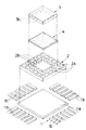
図1〜図6において,符号1は,矩形状のチップマウント部1aと,このチップマウント部1aにおける四つの各辺から外向きに延びる複数本のリード端子1bとを備えたリードフレームを示す。
【0013】
また,符号2は,前記リードフレーム1におけるチップマウント部1aに対してダイボンディングされる第1ICチップを示し,この第1ICチップ2の上面には,図示しない能動素子又は受動素子等のような回路素子の多数個が形成されていると共に,その周囲,つまり,後述する第2ICチップ3より外側の部分にワイヤボンディングパッド2aの多数個が周囲方向に並べて設けられ,更に,その内側に後述する第2ICチップ3に対する接続用の電極パッド2bの多数個が形成されている。また,この第1ICチップ2の上面には,前記各ワイヤボンディングパッド2a及び各電極パッド2bの部分を除く部分に,絶縁性のパシベーション膜2cが形成されている。
【0014】
更にまた,符号3は,前記第1ICチップ2の上面にボンディングされる小さい形状の第2ICチップを示し,この第2ICチップ3における表裏両面のうち少なくとも片面には,前記第1ICチップ2と同様に図示しない能動素子又は受動素子等のような回路素子の多数個が形成されている共に,前記第1ICチップ2における各電極パッド2bの各々に対応する箇所ごとに接続用の電極パッド3aが形成され,この各電極パッド3aの各々には,バンプ3bが,電極パッド3aから突出するように設けられている。
【0015】
そして,前記第2ICチップ3を,その回路素子,電極パッド3a及びバンプ3bを形成した片面を下向きにして,前記第1ICチップ2の上面側に配設し,その間に接着フィルム4を介挿したのち,前記第2ICチップ3を,第1ICチップ2に向かって,その間における前記接着フィルム4を,第2ICチップ3における各バンプ3bと第1ICチップ2における各電極パッド2bとで挟むように押圧し,この押圧を保持した状態で,加熱等にて前記接着フィルム4を乾燥・硬化することにより,前記第2ICチップ3を,第1ICチップ2に対して,図4に示すように,その間に介挿した接着フィルム4を介してボンディングすることができるのである。
【0016】
この場合において,前記接着フィルム4に,図5に示すように,前記バンプ3bの直径よりも小さい内径にした小孔4bの多数個を,当該小孔4bのうち複数個が前記バンプ3bの箇所に位置するようなピッチ間隔で穿設し,この各小孔4b内に,導電粒子の粉末4cを,その導電粒子が互いに接触するような密度で充填するのであり,これにより,第2ICチップ3における各バンプ3bと第1ICチップ2における各電極パッド2bとの間には,前記接着フィルム4に穿設した多数個の小孔4bのうち少なくとも一つ以上の小孔4bが位置することになるから,第2ICチップ3における各電極パッド3aと,第1ICチップ2における各電極パッド2bとの相互間を,前記バンプ3bと電極パッド2bとの間に位置する各小孔4b内に充填した導電粒子の粉末4cによって,電気的に確実に接続することができるのである。
【0017】
このようにして,第1ICチップ2に対して第2ICチップ3をボンディングすると,この第1ICチップ2を,図6に示すように,前記リードフレーム1におけるチップマウント部1aに対してダイボンディングし,次いで,この第1ICチップ2における各ワイヤボンディングパッド2aと,リードフレーム1における各リード端子1bとの間を,細い金属線5によるワイヤボンディングにて電気的に接続したのち,これらの全体を,合成樹脂製のパッケージ体6にて密封することにより,密封型の半導体装置とするのである。 なお,前記の説明は,突出する形態のバンプ3bを,第2ICチップ3における各電極パッド3aに設けた場合であったが,これに代えて,突出する形態のバンプ3bを,第1ICチップ2における各電極パッド2bに設けた構成にしても良いことは言うまでもない。
【図面の簡単な説明】
【図1】 本発明の実施形態を示す分解斜視図である。
【図2】 図1の縦断正面図である。
【図3】 図2の要部拡大図である。
【図4】 第2ICチップを第1ICチップに対してボンディングした状態を示す縦断正面図である。
【図5】 本発明の実施形態に使用する接着フィルムの要部拡大断面図である。
【図6】 密封型半導体装置の縦断正面図である。
【符号の説明】
1 リードフレーム
1a チップマウント部
1b リード端子
2 第1ICチップ
2a 第1ICチップのワイヤボンディングパッド
2b 第1ICチップの電極パッド
3 第2ICチップ
3a 第2ICチップの電極パッド
3b バンプ
4 接着フィルム
4b 小孔
4c 導電粒子の粉末[0001]
BACKGROUND OF THE INVENTION
In the present invention, an IC chip in which a large number of circuit elements are formed is bonded to another IC chip or a circuit board in a state where the electrode pads are electrically connected to each other. The present invention relates to a semiconductor device .
[0002]
[Prior art]
Conventionally, when bonding an IC chip to another IC chip or a circuit board in a state where the respective electrode pads are electrically connected to each other, each electrode pad formed on the IC chip and , Either one of the electrode pads formed on the other IC chip or the circuit board is provided with a bump, and this bump is pressed against the other electrode pad, or the bump is applied to each of both electrode pads. A method is used in which the bumps are crimped together.
[0003]
[Problems to be solved by the invention]
However, in this method, a bump provided on one of the electrode pads of the IC chip and another IC chip or circuit board is pressure-bonded to the other electrode pad, or provided on one electrode pad. In order to crimp the bump on the other electrode pad, a relatively large pressing force must be applied, and the IC chip, the electrode pad, and the bump are likely to be chipped or cracked. There was a problem that the incidence of defective products was high.
[0004]
The present invention has a technical problem to solve these problems.
[0005]
[Means for Solving the Problems]
In order to achieve this technical problem, the present invention
“A first IC chip, a small second IC chip arranged so that the periphery of the first IC chip protrudes from the surface of the first IC chip, and a plurality of leads arranged around the first IC chip. A plurality of wire bonding pads arranged in the peripheral direction on the outer side of the second IC chip on the surface of the first IC chip, the wire bonding pads for wire bonding to the lead terminals, The electrode pad formed on one side of the second IC chip is opposed to the electrode pad formed on the surface of the first IC chip, and each of the electrode pads in the second IC chip and the electrode pads in the first IC chip a bump on one, provided so as to protrude from the electrode pad, the first 2IC chip, the first While adhering to the C chip with an adhesive film interposed therebetween, a large number of small holes penetrating the adhesive film are attached to portions corresponding to the bumps of the adhesive film. A plurality of holes are formed at pitch intervals so as to be located at the bumps , and the small particles are filled with the conductive particle powder so as to be in contact with each other. "
It was made the composition called.
[0006]
[Operation and effect of the invention]
With the above-described configuration, the second IC chip is larger than the second IC chip and is firmly connected to the first IC chip electrically connected to the lead terminal by wire bonding via an adhesive film. At the same time, it can be electrically connected through the conductive particle powder filled in the small holes formed in the adhesive film.
[0007]
In this way, the second IC chip is bonded to the first IC chip which is larger than this and is electrically connected to the lead terminal by wire bonding with an adhesive film interposed therebetween. In some cases, it is considered that the conductive film powder can be electrically connected by mixing the conductive film with the conductive particle powder.
[0008]
However, in order to electrically connect with the conductive particle powder mixed in the adhesive film, the adhesive film must be greatly compressed and deformed by bumps so that the conductive particles come into contact with each other. When the film is compressed and deformed by bumps, the conductive particles mixed in the film escape through the part between the bumps and the electrode pads. The reliability of connection will be reduced.
[0009]
On the other hand, as in the present invention, the adhesive film is provided with a plurality of small holes penetrating the adhesive film, and the conductive particles are filled in the small holes so as to contact each other. In this case, the adhesive film can be electrically connected via the conductive particle powder filled in the small holes formed in the adhesive film without greatly compressing and deforming the adhesive film.
[0010]
Therefore, according to the present invention, the electrode pads are reliably connected to the first IC chip which is larger than the second IC chip and is electrically connected to the lead terminals by wire bonding. The second IC chip can be bonded firmly to the first IC chip while it can be firmly bonded under the condition of being connected to the first IC chip. The process becomes simple and the cost required for this can be greatly reduced. Moreover, since the above-mentioned pressing is much lighter than the conventional bump bonding, the occurrence of chipping or cracking in the IC chip is greatly reduced. It has an effect that it can be reduced.
[0011]
DETAILED DESCRIPTION OF THE INVENTION
Embodiments of the present invention will be described below with reference to the drawings.
[0012]
1 to 6,
[0013]
[0014]
Further,
[0015]
Then, the
[0016]
In this case, as shown in FIG. 5, a plurality of small holes 4b having an inner diameter smaller than the diameter of the
[0017]
When the
[Brief description of the drawings]
FIG. 1 is an exploded perspective view showing an embodiment of the present invention.
FIG. 2 is a longitudinal front view of FIG. 1;
FIG. 3 is an enlarged view of a main part of FIG.
FIG. 4 is a longitudinal front view showing a state where a second IC chip is bonded to the first IC chip.
FIG. 5 is an enlarged cross-sectional view of a main part of an adhesive film used in an embodiment of the present invention.
FIG. 6 is a longitudinal front view of a sealed semiconductor device.
[Explanation of symbols]
DESCRIPTION OF
Claims (1)
Priority Applications (1)
| Application Number | Priority Date | Filing Date | Title |
|---|---|---|---|
| JP03481997A JP3696360B2 (en) | 1997-02-19 | 1997-02-19 | Semiconductor device |
Applications Claiming Priority (1)
| Application Number | Priority Date | Filing Date | Title |
|---|---|---|---|
| JP03481997A JP3696360B2 (en) | 1997-02-19 | 1997-02-19 | Semiconductor device |
Publications (2)
| Publication Number | Publication Date |
|---|---|
| JPH10233406A JPH10233406A (en) | 1998-09-02 |
| JP3696360B2 true JP3696360B2 (en) | 2005-09-14 |
Family
ID=12424821
Family Applications (1)
| Application Number | Title | Priority Date | Filing Date |
|---|---|---|---|
| JP03481997A Expired - Fee Related JP3696360B2 (en) | 1997-02-19 | 1997-02-19 | Semiconductor device |
Country Status (1)
| Country | Link |
|---|---|
| JP (1) | JP3696360B2 (en) |
Families Citing this family (2)
| Publication number | Priority date | Publication date | Assignee | Title |
|---|---|---|---|---|
| JP2002093855A (en) * | 2000-09-18 | 2002-03-29 | Toshiba Corp | Semiconductor device |
| CN113937010B (en) * | 2021-12-16 | 2022-03-29 | 绍兴中芯集成电路制造股份有限公司 | Method for manufacturing semiconductor device |
-
1997
- 1997-02-19 JP JP03481997A patent/JP3696360B2/en not_active Expired - Fee Related
Also Published As
| Publication number | Publication date |
|---|---|
| JPH10233406A (en) | 1998-09-02 |
Similar Documents
| Publication | Publication Date | Title |
|---|---|---|
| JP2914944B2 (en) | Bottom lead package | |
| US7148080B2 (en) | Method for joining lead frames in a package assembly, method for forming a chip stack package, and a chip stack package | |
| US5627405A (en) | Integrated circuit assembly incorporating an anisotropic elecctrically conductive layer | |
| JP3115155B2 (en) | Semiconductor device and manufacturing method thereof | |
| JP3349058B2 (en) | Structure of a semiconductor device having a plurality of IC chips | |
| JP2840316B2 (en) | Semiconductor device and manufacturing method thereof | |
| US8409930B2 (en) | Semiconductor device manufacturing method | |
| US6515357B2 (en) | Semiconductor package and semiconductor package fabrication method | |
| US20040099944A1 (en) | Semiconductor device | |
| US6952047B2 (en) | Assemblies having stacked semiconductor chips and methods of making same | |
| JP2738568B2 (en) | Semiconductor chip module | |
| JP3832102B2 (en) | Manufacturing method of semiconductor device | |
| JP2000332055A (en) | Flip-chip mounting structure and mounting method | |
| US5243497A (en) | Chip on board assembly | |
| JP3696360B2 (en) | Semiconductor device | |
| JP3866777B2 (en) | Semiconductor device and manufacturing method thereof | |
| JP3519924B2 (en) | Semiconductor device structure and method of manufacturing the same | |
| JP3815933B2 (en) | Semiconductor device and manufacturing method thereof | |
| JP3543254B2 (en) | Structure of a semiconductor device having a plurality of IC chips | |
| JP3543253B2 (en) | Structure of a semiconductor device having a plurality of IC chips | |
| JP3543251B2 (en) | IC chip bonding equipment | |
| US6291893B1 (en) | Power semiconductor device for “flip-chip” connections | |
| JP3286196B2 (en) | Structure of sealed semiconductor device having a plurality of IC chips | |
| JP3510520B2 (en) | Semiconductor package and manufacturing method thereof | |
| JP2000252320A (en) | Semiconductor device and manufacture thereof |
Legal Events
| Date | Code | Title | Description |
|---|---|---|---|
| A977 | Report on retrieval |
Free format text: JAPANESE INTERMEDIATE CODE: A971007 Effective date: 20040212 |
|
| A131 | Notification of reasons for refusal |
Free format text: JAPANESE INTERMEDIATE CODE: A131 Effective date: 20040224 |
|
| A521 | Request for written amendment filed |
Free format text: JAPANESE INTERMEDIATE CODE: A523 Effective date: 20040426 |
|
| A131 | Notification of reasons for refusal |
Free format text: JAPANESE INTERMEDIATE CODE: A131 Effective date: 20040720 |
|
| A521 | Request for written amendment filed |
Free format text: JAPANESE INTERMEDIATE CODE: A523 Effective date: 20040913 |
|
| A02 | Decision of refusal |
Free format text: JAPANESE INTERMEDIATE CODE: A02 Effective date: 20041026 |
|
| A521 | Request for written amendment filed |
Free format text: JAPANESE INTERMEDIATE CODE: A523 Effective date: 20041222 |
|
| A911 | Transfer to examiner for re-examination before appeal (zenchi) |
Free format text: JAPANESE INTERMEDIATE CODE: A911 Effective date: 20050106 |
|
| A131 | Notification of reasons for refusal |
Free format text: JAPANESE INTERMEDIATE CODE: A131 Effective date: 20050308 |
|
| A521 | Request for written amendment filed |
Free format text: JAPANESE INTERMEDIATE CODE: A523 Effective date: 20050509 |
|
| TRDD | Decision of grant or rejection written | ||
| A01 | Written decision to grant a patent or to grant a registration (utility model) |
Free format text: JAPANESE INTERMEDIATE CODE: A01 Effective date: 20050621 |
|
| A61 | First payment of annual fees (during grant procedure) |
Free format text: JAPANESE INTERMEDIATE CODE: A61 Effective date: 20050629 |
|
| R150 | Certificate of patent or registration of utility model |
Free format text: JAPANESE INTERMEDIATE CODE: R150 |
|
| FPAY | Renewal fee payment (event date is renewal date of database) |
Free format text: PAYMENT UNTIL: 20110708 Year of fee payment: 6 |
|
| FPAY | Renewal fee payment (event date is renewal date of database) |
Free format text: PAYMENT UNTIL: 20110708 Year of fee payment: 6 |
|
| FPAY | Renewal fee payment (event date is renewal date of database) |
Free format text: PAYMENT UNTIL: 20120708 Year of fee payment: 7 |
|
| LAPS | Cancellation because of no payment of annual fees |