JP3689913B2 - Manufacturing method of thin film piezoelectric element - Google Patents
Manufacturing method of thin film piezoelectric element Download PDFInfo
- Publication number
- JP3689913B2 JP3689913B2 JP51749896A JP51749896A JP3689913B2 JP 3689913 B2 JP3689913 B2 JP 3689913B2 JP 51749896 A JP51749896 A JP 51749896A JP 51749896 A JP51749896 A JP 51749896A JP 3689913 B2 JP3689913 B2 JP 3689913B2
- Authority
- JP
- Japan
- Prior art keywords
- film
- piezoelectric
- manufacturing
- piezoelectric element
- thin film
- Prior art date
- Legal status (The legal status is an assumption and is not a legal conclusion. Google has not performed a legal analysis and makes no representation as to the accuracy of the status listed.)
- Expired - Fee Related
Links
- 239000010409 thin film Substances 0.000 title claims description 37
- 238000004519 manufacturing process Methods 0.000 title claims description 23
- 239000010408 film Substances 0.000 claims description 111
- 238000010438 heat treatment Methods 0.000 claims description 30
- 239000002243 precursor Substances 0.000 claims description 27
- 239000000203 mixture Substances 0.000 claims description 20
- 239000000758 substrate Substances 0.000 claims description 19
- 229910052751 metal Inorganic materials 0.000 claims description 16
- 239000002184 metal Substances 0.000 claims description 16
- 238000009792 diffusion process Methods 0.000 claims description 12
- 238000000034 method Methods 0.000 claims description 12
- QVGXLLKOCUKJST-UHFFFAOYSA-N atomic oxygen Chemical compound [O] QVGXLLKOCUKJST-UHFFFAOYSA-N 0.000 claims description 11
- 239000001301 oxygen Substances 0.000 claims description 11
- 229910052760 oxygen Inorganic materials 0.000 claims description 11
- 239000000463 material Substances 0.000 claims description 7
- 230000002265 prevention Effects 0.000 claims description 7
- 238000004544 sputter deposition Methods 0.000 claims description 7
- 239000013078 crystal Substances 0.000 claims description 6
- 239000011777 magnesium Substances 0.000 claims description 6
- BASFCYQUMIYNBI-UHFFFAOYSA-N platinum Chemical group [Pt] BASFCYQUMIYNBI-UHFFFAOYSA-N 0.000 claims description 6
- 229910052787 antimony Inorganic materials 0.000 claims description 5
- PXHVJJICTQNCMI-UHFFFAOYSA-N nickel Substances [Ni] PXHVJJICTQNCMI-UHFFFAOYSA-N 0.000 claims description 5
- 229910052748 manganese Inorganic materials 0.000 claims description 4
- 229910052759 nickel Inorganic materials 0.000 claims description 4
- RVTZCBVAJQQJTK-UHFFFAOYSA-N oxygen(2-);zirconium(4+) Chemical compound [O-2].[O-2].[Zr+4] RVTZCBVAJQQJTK-UHFFFAOYSA-N 0.000 claims description 4
- 229910001928 zirconium oxide Inorganic materials 0.000 claims description 4
- 229910052793 cadmium Inorganic materials 0.000 claims description 3
- 229910052749 magnesium Inorganic materials 0.000 claims description 3
- 229910052758 niobium Inorganic materials 0.000 claims description 3
- ZBSCCQXBYNSKPV-UHFFFAOYSA-N oxolead;oxomagnesium;2,4,5-trioxa-1$l^{5},3$l^{5}-diniobabicyclo[1.1.1]pentane 1,3-dioxide Chemical compound [Mg]=O.[Pb]=O.[Pb]=O.[Pb]=O.O1[Nb]2(=O)O[Nb]1(=O)O2 ZBSCCQXBYNSKPV-UHFFFAOYSA-N 0.000 claims description 3
- 229910052715 tantalum Inorganic materials 0.000 claims description 3
- 239000011701 zinc Substances 0.000 claims description 3
- 229910052765 Lutetium Inorganic materials 0.000 claims description 2
- 229910052769 Ytterbium Inorganic materials 0.000 claims description 2
- 229910052804 chromium Inorganic materials 0.000 claims description 2
- 238000001816 cooling Methods 0.000 claims description 2
- 229910000449 hafnium oxide Inorganic materials 0.000 claims description 2
- WIHZLLGSGQNAGK-UHFFFAOYSA-N hafnium(4+);oxygen(2-) Chemical compound [O-2].[O-2].[Hf+4] WIHZLLGSGQNAGK-UHFFFAOYSA-N 0.000 claims description 2
- 229910052738 indium Inorganic materials 0.000 claims description 2
- 229910052742 iron Inorganic materials 0.000 claims description 2
- HEPLMSKRHVKCAQ-UHFFFAOYSA-N lead nickel Chemical compound [Ni].[Pb] HEPLMSKRHVKCAQ-UHFFFAOYSA-N 0.000 claims description 2
- JQJCSZOEVBFDKO-UHFFFAOYSA-N lead zinc Chemical compound [Zn].[Pb] JQJCSZOEVBFDKO-UHFFFAOYSA-N 0.000 claims description 2
- DJZHPOJZOWHJPP-UHFFFAOYSA-N magnesium;dioxido(dioxo)tungsten Chemical compound [Mg+2].[O-][W]([O-])(=O)=O DJZHPOJZOWHJPP-UHFFFAOYSA-N 0.000 claims description 2
- 239000012528 membrane Substances 0.000 claims description 2
- TWNQGVIAIRXVLR-UHFFFAOYSA-N oxo(oxoalumanyloxy)alumane Chemical compound O=[Al]O[Al]=O TWNQGVIAIRXVLR-UHFFFAOYSA-N 0.000 claims description 2
- BPUBBGLMJRNUCC-UHFFFAOYSA-N oxygen(2-);tantalum(5+) Chemical compound [O-2].[O-2].[O-2].[O-2].[O-2].[Ta+5].[Ta+5] BPUBBGLMJRNUCC-UHFFFAOYSA-N 0.000 claims description 2
- 229910052697 platinum Inorganic materials 0.000 claims description 2
- 229910052706 scandium Inorganic materials 0.000 claims description 2
- 229910001936 tantalum oxide Inorganic materials 0.000 claims description 2
- ZCUFMDLYAMJYST-UHFFFAOYSA-N thorium dioxide Chemical compound O=[Th]=O ZCUFMDLYAMJYST-UHFFFAOYSA-N 0.000 claims description 2
- 229910003452 thorium oxide Inorganic materials 0.000 claims description 2
- 229910052721 tungsten Inorganic materials 0.000 claims description 2
- 229910052727 yttrium Inorganic materials 0.000 claims description 2
- 229910052725 zinc Inorganic materials 0.000 claims description 2
- 230000004888 barrier function Effects 0.000 claims 1
- 229910052726 zirconium Inorganic materials 0.000 claims 1
- 229910052451 lead zirconate titanate Inorganic materials 0.000 description 18
- 238000010304 firing Methods 0.000 description 12
- 238000005530 etching Methods 0.000 description 10
- 229910021421 monocrystalline silicon Inorganic materials 0.000 description 10
- HTUMBQDCCIXGCV-UHFFFAOYSA-N lead oxide Chemical compound [O-2].[Pb+2] HTUMBQDCCIXGCV-UHFFFAOYSA-N 0.000 description 8
- YEXPOXQUZXUXJW-UHFFFAOYSA-N lead(II) oxide Inorganic materials [Pb]=O YEXPOXQUZXUXJW-UHFFFAOYSA-N 0.000 description 8
- KRHYYFGTRYWZRS-UHFFFAOYSA-N Fluorane Chemical compound F KRHYYFGTRYWZRS-UHFFFAOYSA-N 0.000 description 6
- 238000002425 crystallisation Methods 0.000 description 4
- 230000008025 crystallization Effects 0.000 description 4
- 238000010586 diagram Methods 0.000 description 4
- 238000005245 sintering Methods 0.000 description 4
- 239000010931 gold Substances 0.000 description 3
- QGZKDVFQNNGYKY-UHFFFAOYSA-N Ammonia Chemical compound N QGZKDVFQNNGYKY-UHFFFAOYSA-N 0.000 description 2
- XKRFYHLGVUSROY-UHFFFAOYSA-N Argon Chemical compound [Ar] XKRFYHLGVUSROY-UHFFFAOYSA-N 0.000 description 2
- MHAJPDPJQMAIIY-UHFFFAOYSA-N Hydrogen peroxide Chemical compound OO MHAJPDPJQMAIIY-UHFFFAOYSA-N 0.000 description 2
- KWYUFKZDYYNOTN-UHFFFAOYSA-M Potassium hydroxide Chemical compound [OH-].[K+] KWYUFKZDYYNOTN-UHFFFAOYSA-M 0.000 description 2
- 238000000137 annealing Methods 0.000 description 2
- 229910052788 barium Inorganic materials 0.000 description 2
- 238000006073 displacement reaction Methods 0.000 description 2
- 230000008020 evaporation Effects 0.000 description 2
- 238000001704 evaporation Methods 0.000 description 2
- 239000007789 gas Substances 0.000 description 2
- HFGPZNIAWCZYJU-UHFFFAOYSA-N lead zirconate titanate Chemical compound [O-2].[O-2].[O-2].[O-2].[O-2].[Ti+4].[Zr+4].[Pb+2] HFGPZNIAWCZYJU-UHFFFAOYSA-N 0.000 description 2
- 238000000206 photolithography Methods 0.000 description 2
- 229910052710 silicon Inorganic materials 0.000 description 2
- 239000000243 solution Substances 0.000 description 2
- 238000005477 sputtering target Methods 0.000 description 2
- 229910052712 strontium Inorganic materials 0.000 description 2
- XLYOFNOQVPJJNP-UHFFFAOYSA-N water Substances O XLYOFNOQVPJJNP-UHFFFAOYSA-N 0.000 description 2
- DDFHBQSCUXNBSA-UHFFFAOYSA-N 5-(5-carboxythiophen-2-yl)thiophene-2-carboxylic acid Chemical compound S1C(C(=O)O)=CC=C1C1=CC=C(C(O)=O)S1 DDFHBQSCUXNBSA-UHFFFAOYSA-N 0.000 description 1
- FYYHWMGAXLPEAU-UHFFFAOYSA-N Magnesium Chemical compound [Mg] FYYHWMGAXLPEAU-UHFFFAOYSA-N 0.000 description 1
- 229910052779 Neodymium Inorganic materials 0.000 description 1
- XUIMIQQOPSSXEZ-UHFFFAOYSA-N Silicon Chemical compound [Si] XUIMIQQOPSSXEZ-UHFFFAOYSA-N 0.000 description 1
- 238000002441 X-ray diffraction Methods 0.000 description 1
- 229910021529 ammonia Inorganic materials 0.000 description 1
- 239000007864 aqueous solution Substances 0.000 description 1
- 229910052786 argon Inorganic materials 0.000 description 1
- KVBCYCWRDBDGBG-UHFFFAOYSA-N azane;dihydrofluoride Chemical compound [NH4+].F.[F-] KVBCYCWRDBDGBG-UHFFFAOYSA-N 0.000 description 1
- 229910002056 binary alloy Inorganic materials 0.000 description 1
- 230000032798 delamination Effects 0.000 description 1
- 239000006185 dispersion Substances 0.000 description 1
- PCHJSUWPFVWCPO-UHFFFAOYSA-N gold Chemical compound [Au] PCHJSUWPFVWCPO-UHFFFAOYSA-N 0.000 description 1
- 229910052737 gold Inorganic materials 0.000 description 1
- 239000011261 inert gas Substances 0.000 description 1
- 229910052500 inorganic mineral Inorganic materials 0.000 description 1
- 229910052746 lanthanum Inorganic materials 0.000 description 1
- 238000002844 melting Methods 0.000 description 1
- 230000008018 melting Effects 0.000 description 1
- 239000011707 mineral Substances 0.000 description 1
- 239000011259 mixed solution Substances 0.000 description 1
- 229920002120 photoresistant polymer Polymers 0.000 description 1
- 230000010287 polarization Effects 0.000 description 1
- 230000000630 rising effect Effects 0.000 description 1
- 238000000682 scanning probe acoustic microscopy Methods 0.000 description 1
- 239000010703 silicon Substances 0.000 description 1
- 238000009279 wet oxidation reaction Methods 0.000 description 1
Images

Classifications
-
- B—PERFORMING OPERATIONS; TRANSPORTING
- B41—PRINTING; LINING MACHINES; TYPEWRITERS; STAMPS
- B41J—TYPEWRITERS; SELECTIVE PRINTING MECHANISMS, i.e. MECHANISMS PRINTING OTHERWISE THAN FROM A FORME; CORRECTION OF TYPOGRAPHICAL ERRORS
- B41J2/00—Typewriters or selective printing mechanisms characterised by the printing or marking process for which they are designed
- B41J2/005—Typewriters or selective printing mechanisms characterised by the printing or marking process for which they are designed characterised by bringing liquid or particles selectively into contact with a printing material
- B41J2/01—Ink jet
- B41J2/135—Nozzles
- B41J2/16—Production of nozzles
- B41J2/1621—Manufacturing processes
- B41J2/1626—Manufacturing processes etching
- B41J2/1629—Manufacturing processes etching wet etching
-
- B—PERFORMING OPERATIONS; TRANSPORTING
- B41—PRINTING; LINING MACHINES; TYPEWRITERS; STAMPS
- B41J—TYPEWRITERS; SELECTIVE PRINTING MECHANISMS, i.e. MECHANISMS PRINTING OTHERWISE THAN FROM A FORME; CORRECTION OF TYPOGRAPHICAL ERRORS
- B41J2/00—Typewriters or selective printing mechanisms characterised by the printing or marking process for which they are designed
- B41J2/005—Typewriters or selective printing mechanisms characterised by the printing or marking process for which they are designed characterised by bringing liquid or particles selectively into contact with a printing material
- B41J2/01—Ink jet
- B41J2/135—Nozzles
- B41J2/16—Production of nozzles
- B41J2/1607—Production of print heads with piezoelectric elements
- B41J2/161—Production of print heads with piezoelectric elements of film type, deformed by bending and disposed on a diaphragm
-
- B—PERFORMING OPERATIONS; TRANSPORTING
- B41—PRINTING; LINING MACHINES; TYPEWRITERS; STAMPS
- B41J—TYPEWRITERS; SELECTIVE PRINTING MECHANISMS, i.e. MECHANISMS PRINTING OTHERWISE THAN FROM A FORME; CORRECTION OF TYPOGRAPHICAL ERRORS
- B41J2/00—Typewriters or selective printing mechanisms characterised by the printing or marking process for which they are designed
- B41J2/005—Typewriters or selective printing mechanisms characterised by the printing or marking process for which they are designed characterised by bringing liquid or particles selectively into contact with a printing material
- B41J2/01—Ink jet
- B41J2/135—Nozzles
- B41J2/16—Production of nozzles
- B41J2/1621—Manufacturing processes
- B41J2/1631—Manufacturing processes photolithography
-
- B—PERFORMING OPERATIONS; TRANSPORTING
- B41—PRINTING; LINING MACHINES; TYPEWRITERS; STAMPS
- B41J—TYPEWRITERS; SELECTIVE PRINTING MECHANISMS, i.e. MECHANISMS PRINTING OTHERWISE THAN FROM A FORME; CORRECTION OF TYPOGRAPHICAL ERRORS
- B41J2/00—Typewriters or selective printing mechanisms characterised by the printing or marking process for which they are designed
- B41J2/005—Typewriters or selective printing mechanisms characterised by the printing or marking process for which they are designed characterised by bringing liquid or particles selectively into contact with a printing material
- B41J2/01—Ink jet
- B41J2/135—Nozzles
- B41J2/16—Production of nozzles
- B41J2/1621—Manufacturing processes
- B41J2/164—Manufacturing processes thin film formation
- B41J2/1646—Manufacturing processes thin film formation thin film formation by sputtering
-
- H—ELECTRICITY
- H10—SEMICONDUCTOR DEVICES; ELECTRIC SOLID-STATE DEVICES NOT OTHERWISE PROVIDED FOR
- H10N—ELECTRIC SOLID-STATE DEVICES NOT OTHERWISE PROVIDED FOR
- H10N30/00—Piezoelectric or electrostrictive devices
- H10N30/01—Manufacture or treatment
- H10N30/07—Forming of piezoelectric or electrostrictive parts or bodies on an electrical element or another base
- H10N30/074—Forming of piezoelectric or electrostrictive parts or bodies on an electrical element or another base by depositing piezoelectric or electrostrictive layers, e.g. aerosol or screen printing
- H10N30/076—Forming of piezoelectric or electrostrictive parts or bodies on an electrical element or another base by depositing piezoelectric or electrostrictive layers, e.g. aerosol or screen printing by vapour phase deposition
-
- H—ELECTRICITY
- H10—SEMICONDUCTOR DEVICES; ELECTRIC SOLID-STATE DEVICES NOT OTHERWISE PROVIDED FOR
- H10N—ELECTRIC SOLID-STATE DEVICES NOT OTHERWISE PROVIDED FOR
- H10N30/00—Piezoelectric or electrostrictive devices
- H10N30/20—Piezoelectric or electrostrictive devices with electrical input and mechanical output, e.g. functioning as actuators or vibrators
- H10N30/204—Piezoelectric or electrostrictive devices with electrical input and mechanical output, e.g. functioning as actuators or vibrators using bending displacement, e.g. unimorph, bimorph or multimorph cantilever or membrane benders
- H10N30/2041—Beam type
- H10N30/2042—Cantilevers, i.e. having one fixed end
-
- H—ELECTRICITY
- H10—SEMICONDUCTOR DEVICES; ELECTRIC SOLID-STATE DEVICES NOT OTHERWISE PROVIDED FOR
- H10N—ELECTRIC SOLID-STATE DEVICES NOT OTHERWISE PROVIDED FOR
- H10N30/00—Piezoelectric or electrostrictive devices
- H10N30/20—Piezoelectric or electrostrictive devices with electrical input and mechanical output, e.g. functioning as actuators or vibrators
- H10N30/204—Piezoelectric or electrostrictive devices with electrical input and mechanical output, e.g. functioning as actuators or vibrators using bending displacement, e.g. unimorph, bimorph or multimorph cantilever or membrane benders
- H10N30/2047—Membrane type
-
- H—ELECTRICITY
- H10—SEMICONDUCTOR DEVICES; ELECTRIC SOLID-STATE DEVICES NOT OTHERWISE PROVIDED FOR
- H10N—ELECTRIC SOLID-STATE DEVICES NOT OTHERWISE PROVIDED FOR
- H10N30/00—Piezoelectric or electrostrictive devices
- H10N30/80—Constructional details
- H10N30/85—Piezoelectric or electrostrictive active materials
- H10N30/853—Ceramic compositions
- H10N30/8548—Lead based oxides
- H10N30/8554—Lead zirconium titanate based
-
- B—PERFORMING OPERATIONS; TRANSPORTING
- B41—PRINTING; LINING MACHINES; TYPEWRITERS; STAMPS
- B41J—TYPEWRITERS; SELECTIVE PRINTING MECHANISMS, i.e. MECHANISMS PRINTING OTHERWISE THAN FROM A FORME; CORRECTION OF TYPOGRAPHICAL ERRORS
- B41J2/00—Typewriters or selective printing mechanisms characterised by the printing or marking process for which they are designed
- B41J2/005—Typewriters or selective printing mechanisms characterised by the printing or marking process for which they are designed characterised by bringing liquid or particles selectively into contact with a printing material
- B41J2/01—Ink jet
- B41J2/135—Nozzles
- B41J2/14—Structure thereof only for on-demand ink jet heads
- B41J2002/14387—Front shooter
-
- B—PERFORMING OPERATIONS; TRANSPORTING
- B41—PRINTING; LINING MACHINES; TYPEWRITERS; STAMPS
- B41J—TYPEWRITERS; SELECTIVE PRINTING MECHANISMS, i.e. MECHANISMS PRINTING OTHERWISE THAN FROM A FORME; CORRECTION OF TYPOGRAPHICAL ERRORS
- B41J2202/00—Embodiments of or processes related to ink-jet or thermal heads
- B41J2202/01—Embodiments of or processes related to ink-jet heads
- B41J2202/03—Specific materials used
Description
[発明の背景]
発明の分野
本発明は、電気的エネルギーを機械的エネルギーに変換し、またはその逆を行う薄膜型の圧電体素子に関し、さらに詳しくはアクチュエータ、圧力センサ、温度センサ、インクジェット記録用ヘッドなどに用いられる薄膜型の圧電体素子に関する。
背景技術
チタン酸ジルコン酸鉛(二成分系PZT)に第三成分を加えた三成分系からなる圧電体素子は、その特性において良好であることが知られている。従って、この三成分系PZTにより薄い圧電素子が得られればインクジェット記録ヘッドをより小型化でき有利である。
しかしながら、第三成分系の圧電素子を薄膜の形態で得ようとすると、良好な特性のものが得られ難い。
本発明者らの知る限りでは、従来、薄膜圧電体膜においてその厚さ方向の鉛のばらつきに着目し、それを制御することで良好な薄膜圧電体膜が得られたとする報告はなされていない。
例えば、Applied Physics Letters, 1991, Vol.58,No. 11, 1161-1163には二成分系PZTを用いた強誘電体が開示されている。しかしながら、この報告はこの強誘電体の特性を詳細に開示はしているが、圧電体としての特性の評価は行っていない。
また、特表平5−504740号公報は二成分系PZTを用いた記録ヘッドを開示しているが、三成分系にあってその厚さ方向の鉛のばらつきを制御することが有利であることを開示または示唆するものではない。
[発明の概要]
本発明者等は、今般、三成分系のPZTを用いた薄膜圧電体膜においては、その厚み方向のPb組成のばらつきがその特性に大きく関連するとの知見を得た。さらに、そのばらつきを良好に制御する好適な製造法を確立した。
従って、本発明は、三成分系のPZTを用いた、良好な特性の薄膜圧電体素子の提供をその目的としている。
そして、本発明による薄膜圧電体素子は多結晶体よりなる圧電体膜と、該圧電体膜を挟む二つの電極とを含んでなる薄膜圧電体素子であって、
前記圧電体膜が第三成分を5モル%以上含んでなる三成分系PZTであり、かつその厚さが5μm以下であり、前記圧電体膜におけるその厚み方向のPb組成のばらつきが±5%以下であるものである。
【図面の簡単な説明】
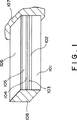
図1は、本発明による薄膜圧電体素子の構造を表す図である。
図2は、本発明による薄膜圧電体素子を用いたインクジェット記録ヘッドの製造法の説明図であって、図2(a)は、その上にSi酸化膜102と、拡散防止膜103と、下電極104と、そして圧電体膜の前駆体膜505が形成された単結晶Si基板101を示し、図2(b)は前駆体膜505を焼成して、圧電体膜105に変換し、更に上電極106を形成した後、インクキャビティー502となる空間がエッチングにより形成された基板101を表し、図2(c)はSi熱酸化膜501およびSi熱酸化膜102がエッチングにより除かれた基板101を表し、そして図2(d)はノズル504が開けられたオリフィスプレート503が接着された基板101を表す図である。
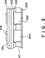
図3は、本発明による薄膜圧電体素子を用いたインクジェット記録ヘッドの別の好ましい構造を表す図である。
[発明の具体的説明]
薄膜圧電体素子
本発明による薄膜圧電体素子は、多結晶体よりなる圧電体膜と、この圧電体膜を挟む二つの電極とから基本的になるものである。そして、圧電体膜が第三成分を5モル%以上含んでなる三成分系PZTであり、かつその厚さが5μm以下であり、また圧電体膜におけるその厚み方向のPb組成のばらつきが±5%以下であるものである。
本発明による圧電体素子は、圧電体膜におけるその厚み方向のPb組成のばらつきが±5%以下と制御された結果、良好な特性を有する。一般に、圧電体素子の変位量は次の式で表現できるとされている。
変位量=a×d31×V=a×ε33×g33×V
(ここで、aは比例定数、d31は圧電定数、ε33は比誘電率、g31は電圧出力係数、そしてVは印加電圧を表す)
本発明の好ましい態様によれば、本発明による薄膜圧電体素子は上記式中にあって、比誘電率ε33は1500以上、より好ましくは2000以上の値を示す。さらに、圧電定数d31にあっては、160pC/N以上、より好ましくは180pC/N以上の値を示す。
本発明の好ましい態様によれば、本発明による薄膜圧電体素子における圧電体の膜厚は1μm〜5μm程度である。
本発明による薄膜圧電体素子は、いわゆる二成分系とよばれるチタン酸ジルコン酸鉛(PZT)に第三成分(例えば、マグネシウムニオブ酸鉛)が更に加えられたものである。ここで、二成分系PZTの好ましい具体例としては、下記の式で表わされる組成を有するものが挙げられる。
Pb(ZrXTi1-X)O3+YPbO
(ここで、0.40≦X≦0.6、0≦Y≦0.3である)
そして、第三成分の好ましい具体例としては、
Pb(AgBh)O3
(式中、
Aは、Mg、Co、Zn、Cd、Mn、およびNiからなる群から選択される2価の金属またはSb、Y、Fe、Sc、Yb、Lu、In、およびCrからなる群から選択される3価の金属を表し、
Bは、Nb、Ta、およびSbからなる群から選択される5価の金属またはWおよびTeからなる群から選択される6価の金属を表し、また
gおよびhは1/2を表すが、但し、Aが3価の金属を表し、かつBが6価の金属を表すことはなく、
またAが2価の金属を表し、かつBが5価の金属を表す場合、gは1/3を表し、hは2/3を表す。)
第三成分の好ましい具体例としては、マグネシウムニオプ酸鉛(Pb(Mg1/3Nb2/3)O3)、亜鉛ニオブ酸鉛(Pb(Zn1/3Nb2/3)O3)、ニッケルニオブ酸鉛(Pb(Ni1/3Nb2/3)O3)、マグネシウムタングステン酸鉛(Pb(Mg1/2W1/2)等が挙げられる。
本発明にあっては、上記組成において第三成分の添加量を5モル%以上、好ましくは10モル%以上、より好ましくは20モル%以上とする。
さらに本発明の好ましい態様によれば、その圧電特性改善するために、微量のBa、Sr、Cd、La、Nd、Nb、Ta、Sb、Bi、W、Mo、Ca、Ni、Mn、Siなどが添加されてもよい。とりわけ、0.10モル%以下のSr、Baの添加が圧電特性の改善にとり好ましい。また、0.10モル%以下のMn、Niの添加がその焼結性を改善するので好ましい。
具体的な薄膜圧電体素子の構造を図面を用いて説明する。図1において、薄膜圧電体素子はシリコン(Si)基板101と、Si熱酸化膜102と、拡散防止膜103、下電極(例えば、Ptからなる)104と、圧電体膜105と、上電極106(例えば、Auからなる)とから構成される。
ここで、拡散防止膜は後記する加熱焼成工程において、圧電体膜からのPbが拡散してSi熱酸化膜に至ることを防止する。PbがSi熱酸化膜に拡散すると、場合によってこのSi熱酸化膜を溶かしてしまうおそれがあるからである。この拡散防止膜は、好ましくは酸化ジルコニウム、酸化トリウム、酸化ハフニウム、酸化タンタル、または酸化アルミニウムからなる。
各層の厚さは適宜決定されてよいが、Si基板は10〜1000μm程度、好ましくは100〜400μm、Si熱酸化膜は0.05〜3μm程度、好ましくは0.1〜1μm、拡散防止膜は0.02〜2μm程度、好ましくは0.04〜1μm、上電極および下電極は0.05〜2μm程度、好ましくは0.1〜0.2程度である。
薄膜圧電体素子の製造
本発明による薄膜圧電体素子は、圧電体膜におけるその厚み方向のPb組成のばらつきが±5%以下と制御された以外は、慣用されている種々の薄膜作製手法を利用して製造されてよい。
好ましい薄膜作製の手法としてはスパッタリングが挙げられる。すなわち、特定成分のPZT焼結体をスパッタリングのターゲットとして用い、電極膜上にスパッタリングによりアモルファス状の圧電体膜前駆体膜を形成する。ここで、この前駆体の組成は、焼結後に第三成分が5モル%以上含んでなる三成分系PZTとなるよう制御される必要がある。本発明の好ましい態様によれば、この前駆体は、化学量論的組成に対してPbを過剰に含むものであるのが好ましい。Pbを10〜30モル%過剰に含んでなるのが好ましく、より好ましくは10〜20モル%である。
次のこのアモルファス状の前駆体を加熱し結晶化し、焼結させる。この加熱は酸素雰囲気中(例えば、酸素中、または酸素とアルゴンなどの不活性ガスとの混合ガス中)において行われる。
本発明者らは、上記の加熱処理にあって、前駆体から拡散するPbOが前駆体表面まで至りPbO皮膜となる現象を確認した。このPbO皮膜が前駆体焼成時に発生するガスの発散を阻害し、層剥離の原因の一つになるものと考えられた。そこで、この前駆体の焼成はPbO皮膜の発生がないように制御して行われるのが好ましい。具体的にはこのPbO皮膜(鉱物名としてMassicotと呼ばれる)の融点と思われる888℃未満の温度において焼成されるのが好ましいといえるが、他の焼成条件を制御することで必ずしも、この温度以上の温度における焼成が本発明の範囲から排除されるものではない。
本発明の好ましい態様によれば、この焼結を一段で行うことが可能である。具体的には、前駆体膜が形成された前記電極を、酸素を含む雰囲気(酸素濃度は好ましくは10〜100%)中で800〜888℃の温度、好ましくは830〜880℃、より好ましくは850〜870℃において加熱する。この加熱は、前駆体膜をペブロスカイト構造の結晶よりなる圧電体膜とするのに十分な時間行う。
また本発明の別の好ましい態様によれば、この焼結を二段階に分けて行うことも可能である。焼成を二段階に分けて行うことで、Pb組成のばらつきをより容易に制御することが可能である。すなわち、一段による焼成にあってはPbの蒸発と結晶化のための焼成とが同時に行われるが、二段による焼成にあっては、まず結晶化のための焼成と、Pbの蒸発を伴う焼成を分けて実施することができるからである(実際には、最初の結晶化のための焼成にあってもPbの蒸発がないわけではない)。具体的な加熱条件は、第1の加熱工程として、酸素を含む雰囲気(酸素濃度は好ましくは10〜100%)中で、前記一段で焼成を行う方法よりも低い温度700〜800℃、好ましくは730〜780℃、より好ましくは750〜770℃において加熱を行う。この加熱は、前駆体膜をペブロスカイト構造の結晶よりなる圧電体膜とするのに十分な時間行う。続いて、第2加熱工程を、加熱温度800〜888℃、好ましくは830〜880℃、より好ましくは850〜870℃程度で実施する。
第1加熱工程と第2加熱工程とは、連続して行われてもよく、また第1加熱工程の後、膜を室温まで冷却した後、第2加熱工程が行われてもよい。
上記焼結は、その結晶化が可能な限り種々の加熱炉を利用することができるが、昇温速度の大きな加熱炉を利用するのが好ましい。例えば、ランプアニール炉の利用が好ましい。好ましい昇温速度としては、上記いずれの方法においても、10℃/秒以上であり、より好ましくは50℃/秒以上である。
以上のように形成された電極上の圧電体膜の上にさらに電極を設け、薄膜圧電体素子とする。
薄膜圧電体素子を用いたインクジェット記録ヘッド
本発明による薄膜圧電体素子は、その良好な特性を利用して、種々の用途に用いられてよい。
例えば、インクジェット記録ヘッドの振動子として利用することができる。本発明による薄膜圧電体素子を利用することで、記録ヘッドの小型化および高解像度化が可能となる。さらに、本発明による圧電体素子は大きな圧力でインクを吐出させることができ、また高い周波数によって駆動が行えるとの利点がある。
本発明による薄膜圧電体素子を利用した好ましい記録ヘッドの断面図は図2(d)に示されるとおりである。この記録ヘッドは、薄膜圧電体素子が設けられ、かつキャビティー502とが設けられた単結晶Si基板101と、ノズル504が設けられたプレート503とからなる。単結晶Si基板101上には、Si熱酸化膜102と、拡散防止膜103、下電極104と、圧電体膜105と、上電極106とから構成される。キャビティー502はインク供給路(図示せず)に通じており、インク供給路から供給されるインク組成物はキャビティー502に溜まる。ここで、圧電体膜105に下電極104と上電極106とを通じて電圧が印加されると、キャビティー502を変形させ、インクに圧力を加える。この圧力によってインクがノズル504より吐出され、インクジェット記録が行える。
このような記録ヘッドは次のような方法によって好ましく製造することができる。図2(a)に示されるように、単結晶Si基板101の両面に、湿式酸化法により、厚み1μmのSi熱酸化膜102および501を形成する。次に、裏面のSi熱酸化膜501をフォトレジストを用いた通常のフォトリソ工程によって、キャビティー502を形成するためにマスクパターンを形成し、Si熱酸化膜501を、フッ酸および弗化アンモニウムの1:10の緩衝弗酸溶液を用いてエッチングを行う。この際、Si熱酸化膜501のパターンが単結晶Si基枚101の結晶方位の面(111)に合うようにする、すなわち図2の単結晶Si基板101の紙面と垂直な面が(111)となるようにするのが好ましい。エッチングのマスクピッチは、ノズルピッチに対応する。高解像度のインクジェット記録ヘッドにあっては、ノズルピッチが例えば140μm程度となるため、エッチングのマスクピッチも同様とする。更に、反対側のSi熱酸化膜102側に、拡散防止膜103、下電極膜104を形成する。さらに、下電極104上全面に圧電体膜の前駆体膜505を形成し、慣用されているフォトリソ工程(例えば、フッ酸系のエッチング液を用いる方法)により、図2(a)に示されているように、インクキャビティー上に、圧電体膜の前駆体膜505を残す。この前駆体膜505を焼成して再結晶させ、圧電体膜105とする。その後、慣用されている方法によって上電極106を形成する。さらに、圧電体膜105および上電極106をマスキングし、単結晶Si基板101をエッチングし、インクキャビティー502を形成する。このエッチングは例えば水酸化カリウム溶液による異方性エッチングによるのが好ましい。例えば、水酸化カリウム溶液の単結晶Siの結晶面方位に対するエッチング選択比は、非常に大きく、(110)面:(111)面=300:1程度である。そのため、インクキャビティー502のような形状を得るためには非常に有利である。
次に、図2(c)に示すように、単結晶Si基板101のエッチングマスクであるSi熱酸化膜501と、インクキャビティー502の上部にあるSi熱酸化膜102をフッ酸−弗化アンモニウム水溶液で、エッチングして除去する。
そして、ノズル504が開けられたオリフィスプレート503を装着して、図2(d)に記載のインクジェット記録ヘッドを得ることができる。
さらに、他の好ましいインクジェット記録ヘッドの断面図は図6に示されるとおりである。この態様では、圧電体膜105をインクキャビティー502の上部全面に形成した例である。
[実施例]
本発明を以下の実施例によって詳細に説明するが、本発明はこれら実施例に限定されるものではない。
実施例1
厚さ400μm、直径4インチの単結晶Si基板を、アンモニア−過酸化水素−水の混合溶液で洗浄した後、水蒸気を含む酸素雰囲気中で1100℃、3時間加熱して湿式酸化を行い、1μmの厚さのSi熱酸化膜を形成した。このSi熱酸化膜の上に、次に高周波スパッタリング法によって、酸化ジルコニウムターゲットを用いて1μmの厚さの酸化ジルコニウム膜を拡散防止膜として形成した。更にこの拡散防止膜上に下部電極としての厚さ0.5μmの白金膜を直流スパッタ法により形成した。
この下部電極上に、スパッタリングターゲットとして組成の制御されたPZTの焼結体を用い、基板温度200℃以下の条件下において高周波スパッタリング法によって、膜厚3μmの圧電体膜前駆体膜を形成した。この前駆体膜はアモルファス状態であった。
前駆体膜が形成されたSi基板をランプアニール装置によって加熱して、前駆体膜を結晶化し、焼結させて圧電体膜とした。加熱条件は、昇温速度100℃/秒として次の第1表に記載の温度まで上昇させ、その後その温度で1分間維持した。また、雰囲気は酸素100%とした。
圧電体膜の上にさらに、直流スパッタ法によって、膜厚0.5μmの金膜を形成し、薄膜圧電体素子とした。
得られたPZT膜の組成は、マグネシウムニオブ酸鉛−ジルコン酸鉛−チタン酸鉛(Pb(Mg1/3Nb2/3)O3−PbZrO3−PbTiO3)の三成分系PZTにおいて、それぞれ40モル%−38モル%−22モル%であった。
また、PZT膜の方向におけるPbの組成分布を、オージェ電子分光法により観察した結果、そのばらつきは次の第1表に示されるとおりであった。
得られた薄膜圧電体素子に分極処理を施した。すなわち、Pt膜およびAu膜間に60Vの電圧を1分間印加した。その後、圧電定数d31を測定した。その値は次の第1表に示されるとおりであった。

実施例2
熱処理条件を860℃、5秒とし、さらに圧電体膜の前駆体におけるPbO組成の過剰量を次の表に示されるように変化させた以外は、実施例1と同様にして薄膜圧電体素子を得た。
得られた圧電体素子のPbのばらつきと、圧電定数は次の第2表に示されるとおりであった。
熱処理を二段階に分けて実施した以外は、実施例1と同様にして薄膜圧電体素子を得た。第一の熱処理は次の第3表に示される温度で1分間、また第二の熱処理は870℃で1分間行った。
得られた圧電体素子のPbのばらつきと、圧電定数は次の第3表に示されるとおりであった。
Field of the Invention The present invention relates to a thin film type piezoelectric element that converts electrical energy into mechanical energy and vice versa, and more specifically, an actuator, a pressure sensor, a temperature sensor, and an inkjet recording head. The present invention relates to a thin film type piezoelectric element used for such as.
BACKGROUND ART It is known that a piezoelectric element composed of a ternary system in which a third component is added to lead zirconate titanate (binary system PZT) has good characteristics. Therefore, if a thin piezoelectric element can be obtained by this three-component PZT, it is advantageous that the ink jet recording head can be further downsized.
However, if a third component type piezoelectric element is obtained in the form of a thin film, it is difficult to obtain one having good characteristics.
As far as the present inventors know, there has been no report that a thin film piezoelectric film has been obtained by focusing on and controlling the lead variation in the thickness direction of the thin film piezoelectric film. .
For example, Applied Physics Letters, 1991, Vol. 58, No. 11, 1161-1163 discloses a ferroelectric using a two-component PZT. However, although this report discloses the characteristics of the ferroelectric material in detail, the characteristics as a piezoelectric material are not evaluated.
Also, Japanese Patent Publication No. 5-504740 discloses a recording head using a two-component system PZT. However, it is advantageous to control the variation of lead in the thickness direction in a three-component system. Is not disclosed or suggested.
[Summary of Invention]
The present inventors have recently found that in a thin film piezoelectric film using ternary PZT, variations in the Pb composition in the thickness direction are largely related to the characteristics. Furthermore, the suitable manufacturing method which controls the dispersion | variation favorably was established.
Accordingly, an object of the present invention is to provide a thin film piezoelectric element having good characteristics using ternary PZT.
The thin film piezoelectric element according to the present invention is a thin film piezoelectric element including a piezoelectric film made of a polycrystal and two electrodes sandwiching the piezoelectric film,
The piezoelectric film is a ternary PZT containing 5 mol% or more of the third component and has a thickness of 5 μm or less, and the Pb composition variation in the thickness direction of the piezoelectric film is ± 5%. It is the following.
[Brief description of the drawings]
FIG. 1 is a diagram showing the structure of a thin film piezoelectric element according to the present invention.
FIG. 2 is an explanatory diagram of a method of manufacturing an ink jet recording head using a thin film piezoelectric element according to the present invention. FIG. 2 (a) shows a
FIG. 3 is a diagram showing another preferred structure of an ink jet recording head using the thin film piezoelectric element according to the present invention.
[Detailed Description of the Invention]
Thin film piezoelectric element The thin film piezoelectric element according to the present invention is basically composed of a piezoelectric film made of a polycrystalline material and two electrodes sandwiching the piezoelectric film. The piezoelectric film is a three-component PZT containing 5 mol% or more of the third component and has a thickness of 5 μm or less, and the Pb composition variation in the thickness direction in the piezoelectric film is ± 5. % Or less.
The piezoelectric element according to the present invention has good characteristics as a result of controlling the variation of the Pb composition in the thickness direction of the piezoelectric film to be ± 5% or less. In general, the displacement amount of a piezoelectric element can be expressed by the following equation.
Displacement amount = a × d31 × V = a × ε33 × g33 × V
(Where a is a proportional constant, d31 is a piezoelectric constant, ε33 is a relative dielectric constant, g31 is a voltage output coefficient, and V is an applied voltage)
According to a preferred embodiment of the present invention, the thin film piezoelectric element according to the present invention is in the above formula, and the relative dielectric constant ε33 is 1500 or more, more preferably 2000 or more. Furthermore, in the piezoelectric constant d31, the value is 160 pC / N or more, more preferably 180 pC / N or more.
According to a preferred aspect of the present invention, the film thickness of the piezoelectric body in the thin film piezoelectric element according to the present invention is about 1 μm to 5 μm.
The thin film piezoelectric element according to the present invention is obtained by further adding a third component (for example, lead magnesium niobate) to lead zirconate titanate (PZT) called a so-called two-component system. Here, preferred specific examples of the two-component PZT include those having a composition represented by the following formula.
Pb (Zr X Ti 1-X ) O 3 + YPbO
(Where 0.40 ≦ X ≦ 0.6 and 0 ≦ Y ≦ 0.3)
And as a preferable specific example of the third component,
Pb (A g B h ) O 3
(Where
A is selected from a divalent metal selected from the group consisting of Mg, Co, Zn, Cd, Mn, and Ni or a group consisting of Sb, Y, Fe, Sc, Yb, Lu, In, and Cr. Represents a trivalent metal,
B represents a pentavalent metal selected from the group consisting of Nb, Ta, and Sb or a hexavalent metal selected from the group consisting of W and Te, and g and h represent 1/2, However, A does not represent a trivalent metal and B does not represent a hexavalent metal,
When A represents a divalent metal and B represents a pentavalent metal, g represents 1/3 and h represents 2/3. )
Preferable specific examples of the third component include lead magnesium niobate (Pb (Mg 1/3 Nb 2/3 ) O 3 ), lead zinc niobate (Pb (Zn 1/3 Nb 2/3 ) O 3 ). And lead nickel niobate (Pb (Ni 1/3 Nb 2/3 ) O 3 ) and lead magnesium tungstate (Pb (Mg 1/2 W 1/2 )).
In the present invention, the amount of the third component added in the above composition is 5 mol% or more, preferably 10 mol% or more, more preferably 20 mol% or more.
Furthermore, according to a preferred aspect of the present invention, a small amount of Ba, Sr, Cd, La, Nd, Nb, Ta, Sb, Bi, W, Mo, Ca, Ni, Mn, Si, etc. are used to improve the piezoelectric characteristics. May be added. In particular, addition of 0.10 mol% or less of Sr and Ba is preferable for improving the piezoelectric characteristics. Further, addition of 0.10 mol% or less of Mn and Ni is preferable because the sinterability is improved.
A specific structure of the thin film piezoelectric element will be described with reference to the drawings. In FIG. 1, a thin film piezoelectric element includes a silicon (Si)
Here, the diffusion preventing film prevents Pb from the piezoelectric film from diffusing and reaching the Si thermal oxide film in the heating and baking process described later. This is because if Pb diffuses into the Si thermal oxide film, the Si thermal oxide film may be dissolved in some cases. This diffusion prevention film is preferably made of zirconium oxide, thorium oxide, hafnium oxide, tantalum oxide, or aluminum oxide.
The thickness of each layer may be determined as appropriate, but the Si substrate is about 10 to 1000 μm, preferably 100 to 400 μm, the Si thermal oxide film is about 0.05 to 3 μm, preferably 0.1 to 1 μm, and the diffusion prevention film is About 0.02 to 2 μm, preferably 0.04 to 1 μm, and the upper and lower electrodes are about 0.05 to 2 μm, preferably about 0.1 to 0.2.
Production of thin film piezoelectric element The thin film piezoelectric element according to the present invention is a variety of commonly used thin films except that the variation in the Pb composition in the thickness direction of the piezoelectric film is controlled to be ± 5% or less. It may be manufactured using a production technique.
A preferable method for forming a thin film is sputtering. That is, a PZT sintered body having a specific component is used as a sputtering target, and an amorphous piezoelectric film precursor film is formed on the electrode film by sputtering. Here, the composition of this precursor needs to be controlled so that it becomes a ternary PZT containing 5 mol% or more of the third component after sintering. According to a preferred embodiment of the present invention, the precursor preferably contains an excess of Pb with respect to the stoichiometric composition. Pb is preferably contained in an excess of 10 to 30 mol%, more preferably 10 to 20 mol%.
Next, this amorphous precursor is heated, crystallized and sintered. This heating is performed in an oxygen atmosphere (for example, in oxygen or a mixed gas of oxygen and an inert gas such as argon).
The inventors of the present invention have confirmed a phenomenon in which the PbO diffused from the precursor reaches the precursor surface and becomes a PbO film in the above heat treatment. This PbO film was thought to inhibit gas divergence generated during firing of the precursor and to be one of the causes of delamination. Therefore, it is preferable to perform the firing of the precursor in a controlled manner so that no PbO film is generated. Specifically, it can be said that firing is preferably performed at a temperature of less than 888 ° C., which is considered to be the melting point of the PbO film (named as Massicot as a mineral name). Firing at this temperature is not excluded from the scope of the present invention.
According to a preferred embodiment of the present invention, this sintering can be performed in one step. Specifically, the electrode on which the precursor film is formed is heated to 800 to 888 ° C. in an atmosphere containing oxygen (oxygen concentration is preferably 10 to 100%), preferably 830 to 880 ° C., more preferably Heat at 850-870 ° C. This heating is performed for a time sufficient to make the precursor film a piezoelectric film made of a crystal having a perovskite structure.
According to another preferred embodiment of the present invention, this sintering can be performed in two stages. By performing the firing in two stages, it is possible to more easily control the variation in the Pb composition. In other words, Pb evaporation and crystallization firing are performed at the same time in one-stage firing, but in two-stage firing, first, firing for crystallization and firing with Pb evaporation. (In practice, Pb does not evaporate even in the first crystallization firing). The specific heating conditions are as follows. As the first heating step, in an atmosphere containing oxygen (oxygen concentration is preferably 10 to 100%), the temperature is 700 to 800 ° C., which is lower than the method of firing in one step, preferably Heating is performed at 730 to 780 ° C, more preferably 750 to 770 ° C. This heating is performed for a time sufficient to make the precursor film a piezoelectric film made of a crystal having a perovskite structure. Then, a 2nd heating process is implemented at the heating temperature of 800-888 degreeC, Preferably it is 830-880 degreeC, More preferably, it is about 850-870 degreeC.
A 1st heating process and a 2nd heating process may be performed continuously, and after cooling a film | membrane to room temperature after a 1st heating process, a 2nd heating process may be performed.
For the sintering, various heating furnaces can be used as long as the crystallization is possible, but it is preferable to use a heating furnace having a high temperature rising rate. For example, it is preferable to use a lamp annealing furnace. A preferable temperature increase rate is 10 ° C./second or more, more preferably 50 ° C./second or more, in any of the above methods.
An electrode is further provided on the piezoelectric film on the electrode formed as described above to form a thin film piezoelectric element.
Ink jet recording head using thin film piezoelectric element The thin film piezoelectric element according to the present invention may be used for various applications by utilizing its good characteristics.
For example, it can be used as a vibrator of an ink jet recording head. By using the thin film piezoelectric element according to the present invention, it is possible to reduce the size and the resolution of the recording head. Furthermore, the piezoelectric element according to the present invention has an advantage that it can eject ink with a large pressure and can be driven at a high frequency.
A cross-sectional view of a preferred recording head using the thin film piezoelectric element according to the present invention is as shown in FIG. This recording head comprises a single
Such a recording head can be preferably manufactured by the following method. As shown in FIG. 2A, Si
Next, as shown in FIG. 2C, the Si
Then, the ink jet recording head shown in FIG. 2D can be obtained by mounting the
Further, a cross-sectional view of another preferred ink jet recording head is as shown in FIG. In this embodiment, the
[Example]
The present invention will be described in detail by the following examples, but the present invention is not limited to these examples.
Example 1
A single crystal Si substrate having a thickness of 400 μm and a diameter of 4 inches is washed with a mixed solution of ammonia, hydrogen peroxide, and water, and then wet-oxidized by heating at 1100 ° C. for 3 hours in an oxygen atmosphere containing water vapor. A Si thermal oxide film having a thickness of 5 mm was formed. Next, a zirconium oxide film having a thickness of 1 μm was formed as a diffusion preventing film on the Si thermal oxide film by a high frequency sputtering method using a zirconium oxide target. Further, a platinum film having a thickness of 0.5 μm as a lower electrode was formed on the diffusion preventing film by a direct current sputtering method.
A piezoelectric film precursor film having a film thickness of 3 μm was formed on the lower electrode by a high-frequency sputtering method using a PZT sintered body having a controlled composition as a sputtering target under a substrate temperature of 200 ° C. or lower. This precursor film was in an amorphous state.
The Si substrate on which the precursor film was formed was heated by a lamp annealing device, and the precursor film was crystallized and sintered to obtain a piezoelectric film. As heating conditions, the temperature was raised to a temperature shown in Table 1 below at a rate of temperature increase of 100 ° C./second, and then maintained at that temperature for 1 minute. The atmosphere was 100% oxygen.
A gold film having a film thickness of 0.5 μm was further formed on the piezoelectric film by direct current sputtering to obtain a thin film piezoelectric element.
The composition of the obtained PZT film is as follows: ternary PZT of lead magnesium niobate-lead zirconate-lead titanate (Pb (Mg 1/3 Nb 2/3 ) O 3 —PbZrO 3 —PbTiO 3 ) It was 40 mol% -38 mol% -22 mol%.
Further, as a result of observing the composition distribution of Pb in the direction of the PZT film by Auger electron spectroscopy, the variation was as shown in Table 1 below.
The obtained thin film piezoelectric element was subjected to polarization treatment. That is, a voltage of 60 V was applied for 1 minute between the Pt film and the Au film. Thereafter, the piezoelectric constant d31 was measured. The values were as shown in Table 1 below.
Example 2
A thin film piezoelectric element was fabricated in the same manner as in Example 1 except that the heat treatment condition was 860 ° C., 5 seconds, and the PbO composition excess in the piezoelectric film precursor was changed as shown in the following table. Obtained.
The variation of Pb and the piezoelectric constant of the obtained piezoelectric element were as shown in the following Table 2.
A thin film piezoelectric element was obtained in the same manner as in Example 1 except that the heat treatment was performed in two stages. The first heat treatment was performed at the temperature shown in Table 3 below for 1 minute, and the second heat treatment was performed at 870 ° C. for 1 minute.
The variation of Pb and the piezoelectric constant of the obtained piezoelectric element were as shown in Table 3 below.
Claims (18)
前記圧電体膜が第三成分を5モル%以上含んでなる三成分系PZTであり、かつその厚さが5μm以下であり、前記圧電体膜におけるその厚み方向のPb組成のばらつきが±5%以下であり、該方法が、
電極上に化学量論的組成に対してPbが過剰である、圧電体の前駆体膜を形成する工程と、
前駆体膜が形成された前記電極を、酸素を含む雰囲気中で700〜800℃の温度で加熱し、前記前駆体膜をペブロスカイト構造の結晶よりなる圧電体膜とする第1加熱工程と、そして
圧電体膜が形成された前記電極を、酸素を含む雰囲気中で800〜888℃の温度で加熱し、前記圧電体膜を更に緻密に結晶化させる第2加熱工程と
を含んでなる、方法。A method of manufacturing a thin film piezoelectric element comprising a piezoelectric film made of a polycrystalline material and two electrodes sandwiching the piezoelectric film,
The piezoelectric film is a ternary PZT containing 5 mol% or more of the third component and has a thickness of 5 μm or less, and the Pb composition variation in the thickness direction of the piezoelectric film is ± 5%. And the method comprises:
Forming a piezoelectric precursor film having an excess of Pb relative to the stoichiometric composition on the electrode;
A first heating step in which the electrode on which the precursor film is formed is heated at a temperature of 700 to 800 ° C. in an oxygen-containing atmosphere so that the precursor film is a piezoelectric film made of a crystal having a perovskite structure; and And a second heating step in which the electrode on which the piezoelectric film is formed is heated at a temperature of 800 to 888 ° C. in an oxygen-containing atmosphere to crystallize the piezoelectric film more densely.
Pb(AgBh)O3
(式中、
Aは、Mg、Co、Zn、Cd、Mn、およびNiからなる群から選択される2価の金属またはSb、Y、Fe、Sc、Yb、Lu、In、およびCrからなる群から選択される3価の金属を表し、
Bは、Nb、Ta、およびSbからなる群から選択される5価の金属またはWおよびTeからなる群から選択される6価の金属を表し、また
gおよびhは1/2を表すが、但し、Aが3価の金属を表し、かつBが6価の金属を表すことはなく、
またAが2価の金属を表し、かつBが5価の金属を表す場合、gは1/3を表し、hは2/3を表す。)The production method according to any one of claims 1 to 9, wherein the third component is represented by the following formula:
Pb (AgBh) O 3
(Where
A is selected from a divalent metal selected from the group consisting of Mg, Co, Zn, Cd, Mn, and Ni or a group consisting of Sb, Y, Fe, Sc, Yb, Lu, In, and Cr. Represents a trivalent metal,
B represents a pentavalent metal selected from the group consisting of Nb, Ta, and Sb or a hexavalent metal selected from the group consisting of W and Te, and g and h represent 1/2, However, A does not represent a trivalent metal and B does not represent a hexavalent metal,
When A represents a divalent metal and B represents a pentavalent metal, g represents 1/3 and h represents 2/3. )
Applications Claiming Priority (2)
| Application Number | Priority Date | Filing Date | Title |
|---|---|---|---|
| JP32563394 | 1994-12-27 | ||
| PCT/JP1995/002721 WO1996020503A1 (en) | 1994-12-27 | 1995-12-27 | Thin-film piezoelectric element, process for preparing the same, and ink jet recording head made by using said element |
Publications (1)
| Publication Number | Publication Date |
|---|---|
| JP3689913B2 true JP3689913B2 (en) | 2005-08-31 |
Family
ID=18179031
Family Applications (1)
| Application Number | Title | Priority Date | Filing Date |
|---|---|---|---|
| JP51749896A Expired - Fee Related JP3689913B2 (en) | 1994-12-27 | 1995-12-27 | Manufacturing method of thin film piezoelectric element |
Country Status (5)
| Country | Link |
|---|---|
| US (1) | US5814923A (en) |
| EP (1) | EP0747976B1 (en) |
| JP (1) | JP3689913B2 (en) |
| DE (1) | DE69517417T2 (en) |
| WO (1) | WO1996020503A1 (en) |
Families Citing this family (19)
| Publication number | Priority date | Publication date | Assignee | Title |
|---|---|---|---|---|
| JP3713921B2 (en) * | 1996-10-24 | 2005-11-09 | セイコーエプソン株式会社 | Method for manufacturing ink jet recording head |
| JP3682684B2 (en) * | 1997-10-20 | 2005-08-10 | セイコーエプソン株式会社 | Method for manufacturing piezoelectric thin film element |
| WO1999045598A1 (en) * | 1998-03-04 | 1999-09-10 | Seiko Epson Corporation | Piezoelectric device, ink-jet recording head, method fo manufacture, and printer |
| JP2001057449A (en) * | 1999-06-08 | 2001-02-27 | Matsushita Electric Ind Co Ltd | Thin plate piezoelectric element, piezoelectric oscillator and voice generator utilizing it |
| US20030189241A1 (en) * | 2000-09-27 | 2003-10-09 | Takeshi Kamada | Dielectric thin film element, actuator comprising it, ink jet head, and ink jet recorder |
| DE60238599D1 (en) * | 2001-03-12 | 2011-01-27 | Ngk Insulators Ltd | TYPE-ACTUATOR WITH PIEZOELECTIVE / ELECTROSTRICTIVE FILM AND METHOD FOR THE PRODUCTION THEREOF |
| US6620237B2 (en) | 2001-11-15 | 2003-09-16 | Spectra, Inc. | Oriented piezoelectric film |
| EP1616700A1 (en) * | 2004-07-13 | 2006-01-18 | Brother Kogyo Kabushiki Kaisha | Piezoelectric actuator, ink jet head, and method of manufacturing them |
| US7419252B2 (en) | 2004-07-13 | 2008-09-02 | Brother Kogyo Kabushiki Kaisha | Ink jet head, piezo-electric actuator, and method of manufacturing them |
| JP5123532B2 (en) * | 2007-01-30 | 2013-01-23 | 太陽誘電株式会社 | Micro cantilever |
| JP4276276B2 (en) * | 2007-09-07 | 2009-06-10 | 富士フイルム株式会社 | Method for manufacturing piezoelectric element |
| DE102007045089A1 (en) * | 2007-09-07 | 2009-03-12 | Epcos Ag | Ceramic material, method for producing the same and electroceramic component comprising the ceramic material |
| CN102077457B (en) * | 2008-07-02 | 2013-06-26 | 阿尔卑斯电气株式会社 | Polymeric actuator and device equipped with polymeric actuator |
| JP5444662B2 (en) * | 2008-08-25 | 2014-03-19 | ソニー株式会社 | Method for manufacturing piezoelectric device |
| JP5585209B2 (en) * | 2009-05-28 | 2014-09-10 | 株式会社リコー | Electromechanical transducer manufacturing method, electromechanical transducer manufactured by the manufacturing method, droplet ejection head, and droplet ejection apparatus |
| WO2011021464A1 (en) * | 2009-08-20 | 2011-02-24 | 株式会社村田製作所 | Manufacturing method of laminated ceramic capacitor, and laminated ceramic capacitor |
| JP2012215518A (en) * | 2011-04-01 | 2012-11-08 | Rohm Co Ltd | Piezoelectric thin film structure, and angle speed detector |
| KR101776237B1 (en) * | 2015-05-21 | 2017-09-11 | 연세대학교 산학협력단 | Pad for sensing of snoring and sleep apnea |
| JP2017080946A (en) * | 2015-10-26 | 2017-05-18 | セイコーエプソン株式会社 | Method of manufacturing mems device, mems device, liquid injection head, and liquid injection device |
Family Cites Families (21)
| Publication number | Priority date | Publication date | Assignee | Title |
|---|---|---|---|---|
| JPS54105799A (en) * | 1978-02-07 | 1979-08-20 | Toshiba Corp | Compound piezo-electric unit and preparation |
| US4565642A (en) * | 1982-07-14 | 1986-01-21 | Hitachi, Ltd. | Piezoelectric substances |
| US4636908A (en) * | 1983-01-31 | 1987-01-13 | Nippon Soda Co., Ltd. | Thin-film dielectric and process for its production |
| JPS63238799A (en) * | 1986-12-12 | 1988-10-04 | Fuji Electric Co Ltd | Manufacture of piezo-electric type vibrator |
| US4862029A (en) * | 1987-02-11 | 1989-08-29 | Tosoh Corporation | Actuator |
| JPH0762235B2 (en) * | 1987-10-05 | 1995-07-05 | 松下電器産業株式会社 | Method of manufacturing ferroelectric thin film |
| JPH02248089A (en) * | 1989-03-22 | 1990-10-03 | Toshiba Corp | Electronic component |
| US5032471A (en) * | 1989-03-24 | 1991-07-16 | Mitsubishi Mining And Cement Co. Ltd. | Pyroelectric ceramic composition and multilayered structure therefrom |
| US5141903A (en) * | 1989-03-31 | 1992-08-25 | Mitsubishi Mining And Cement Co. Ltd. | Pyroelectric ceramic composition |
| JP2886588B2 (en) * | 1989-07-11 | 1999-04-26 | 日本碍子株式会社 | Piezoelectric / electrostrictive actuator |
| JPH03112863A (en) * | 1989-09-28 | 1991-05-14 | Mitsubishi Materials Corp | Piezoelectric ceramic sintered composition |
| JPH07108102B2 (en) * | 1990-05-01 | 1995-11-15 | 日本碍子株式会社 | Method for manufacturing piezoelectric / electrostrictive film type actuator |
| US5210455A (en) * | 1990-07-26 | 1993-05-11 | Ngk Insulators, Ltd. | Piezoelectric/electrostrictive actuator having ceramic substrate having recess defining thin-walled portion |
| CN1025703C (en) * | 1990-10-29 | 1994-08-17 | 湖北大学 | High power piezoelectric ceramic material |
| JPH06235268A (en) * | 1991-05-21 | 1994-08-23 | Kiyoshi Tokunaga | Transverse warehousing and delivering system parking garage for vehicle |
| EP0526048B1 (en) * | 1991-07-18 | 1997-11-12 | Ngk Insulators, Ltd. | Piezoelectric/electrostrictive element having ceramic substrate formed essentially of stabilized zirconia |
| JP3182909B2 (en) * | 1991-09-25 | 2001-07-03 | セイコーエプソン株式会社 | Method of manufacturing ferroelectric capacitor and method of manufacturing ferroelectric memory device |
| JP3144949B2 (en) * | 1992-05-27 | 2001-03-12 | 日本碍子株式会社 | Piezoelectric / electrostrictive actuator |
| US5645753A (en) * | 1994-05-19 | 1997-07-08 | Kyocera Corporation | Piezo-electric ceramic composition |
| US5825121A (en) * | 1994-07-08 | 1998-10-20 | Seiko Epson Corporation | Thin film piezoelectric device and ink jet recording head comprising the same |
| US5658485A (en) * | 1995-10-03 | 1997-08-19 | Lucent Technologies Inc. | Pyrochlore based oxides with high dielectric constant and low temperature coefficient |
-
1995
- 1995-12-27 US US08/696,914 patent/US5814923A/en not_active Expired - Lifetime
- 1995-12-27 EP EP95942281A patent/EP0747976B1/en not_active Expired - Lifetime
- 1995-12-27 WO PCT/JP1995/002721 patent/WO1996020503A1/en active IP Right Grant
- 1995-12-27 JP JP51749896A patent/JP3689913B2/en not_active Expired - Fee Related
- 1995-12-27 DE DE69517417T patent/DE69517417T2/en not_active Expired - Lifetime
Also Published As
| Publication number | Publication date |
|---|---|
| US5814923A (en) | 1998-09-29 |
| EP0747976B1 (en) | 2000-06-07 |
| WO1996020503A1 (en) | 1996-07-04 |
| DE69517417D1 (en) | 2000-07-13 |
| DE69517417T2 (en) | 2000-10-26 |
| EP0747976A4 (en) | 1999-03-31 |
| EP0747976A1 (en) | 1996-12-11 |
Similar Documents
| Publication | Publication Date | Title |
|---|---|---|
| JP3689913B2 (en) | Manufacturing method of thin film piezoelectric element | |
| US5825121A (en) | Thin film piezoelectric device and ink jet recording head comprising the same | |
| US5802686A (en) | Process for the preparation of an ink jet printer head | |
| JP4618196B2 (en) | Piezoelectric actuator and ink jet recording head | |
| JP5245107B2 (en) | Piezoelectric element, piezoelectric actuator, ink jet recording head | |
| US20080199599A1 (en) | Method of manufacturing dielectric layer and method of manufacturing liquid jet head | |
| JP3381473B2 (en) | Liquid jet head | |
| JP5370346B2 (en) | Piezoelectric element and ink jet recording head | |
| JP3582550B2 (en) | Method of manufacturing printer head for inkjet recording | |
| JP3734176B2 (en) | Method for manufacturing printer head for inkjet recording and method for manufacturing actuator | |
| JP3371391B2 (en) | Thin film piezoelectric element and ink jet recording head using the same | |
| JP2003008096A (en) | Piezoelectric/electrostrictive film element |
Legal Events
| Date | Code | Title | Description |
|---|---|---|---|
| A131 | Notification of reasons for refusal |
Free format text: JAPANESE INTERMEDIATE CODE: A131 Effective date: 20040113 |
|
| A521 | Request for written amendment filed |
Free format text: JAPANESE INTERMEDIATE CODE: A523 Effective date: 20040315 |
|
| A131 | Notification of reasons for refusal |
Free format text: JAPANESE INTERMEDIATE CODE: A131 Effective date: 20050315 |
|
| A521 | Request for written amendment filed |
Free format text: JAPANESE INTERMEDIATE CODE: A523 Effective date: 20050328 |
|
| TRDD | Decision of grant or rejection written | ||
| A01 | Written decision to grant a patent or to grant a registration (utility model) |
Free format text: JAPANESE INTERMEDIATE CODE: A01 Effective date: 20050524 |
|
| A61 | First payment of annual fees (during grant procedure) |
Free format text: JAPANESE INTERMEDIATE CODE: A61 Effective date: 20050606 |
|
| R150 | Certificate of patent or registration of utility model |
Free format text: JAPANESE INTERMEDIATE CODE: R150 |
|
| FPAY | Renewal fee payment (event date is renewal date of database) |
Free format text: PAYMENT UNTIL: 20090624 Year of fee payment: 4 |
|
| FPAY | Renewal fee payment (event date is renewal date of database) |
Free format text: PAYMENT UNTIL: 20100624 Year of fee payment: 5 |
|
| FPAY | Renewal fee payment (event date is renewal date of database) |
Free format text: PAYMENT UNTIL: 20110624 Year of fee payment: 6 |
|
| FPAY | Renewal fee payment (event date is renewal date of database) |
Free format text: PAYMENT UNTIL: 20110624 Year of fee payment: 6 |
|
| FPAY | Renewal fee payment (event date is renewal date of database) |
Free format text: PAYMENT UNTIL: 20120624 Year of fee payment: 7 |
|
| LAPS | Cancellation because of no payment of annual fees |