JP3689757B2 - Method for forming gate electrode of semiconductor element - Google Patents
Method for forming gate electrode of semiconductor element Download PDFInfo
- Publication number
- JP3689757B2 JP3689757B2 JP35270099A JP35270099A JP3689757B2 JP 3689757 B2 JP3689757 B2 JP 3689757B2 JP 35270099 A JP35270099 A JP 35270099A JP 35270099 A JP35270099 A JP 35270099A JP 3689757 B2 JP3689757 B2 JP 3689757B2
- Authority
- JP
- Japan
- Prior art keywords
- film
- gate electrode
- forming
- gate
- metal
- Prior art date
- Legal status (The legal status is an assumption and is not a legal conclusion. Google has not performed a legal analysis and makes no representation as to the accuracy of the status listed.)
- Expired - Fee Related
Links
Images


Classifications
-
- H—ELECTRICITY
- H10—SEMICONDUCTOR DEVICES; ELECTRIC SOLID-STATE DEVICES NOT OTHERWISE PROVIDED FOR
- H10D—INORGANIC ELECTRIC SEMICONDUCTOR DEVICES
- H10D64/00—Electrodes of devices having potential barriers
- H10D64/60—Electrodes characterised by their materials
- H10D64/66—Electrodes having a conductor capacitively coupled to a semiconductor by an insulator, e.g. MIS electrodes
- H10D64/661—Electrodes having a conductor capacitively coupled to a semiconductor by an insulator, e.g. MIS electrodes the conductor comprising a layer of silicon contacting the insulator, e.g. polysilicon having vertical doping variation
- H10D64/662—Electrodes having a conductor capacitively coupled to a semiconductor by an insulator, e.g. MIS electrodes the conductor comprising a layer of silicon contacting the insulator, e.g. polysilicon having vertical doping variation the conductor further comprising additional layers, e.g. multiple silicon layers having different crystal structures
- H10D64/664—Electrodes having a conductor capacitively coupled to a semiconductor by an insulator, e.g. MIS electrodes the conductor comprising a layer of silicon contacting the insulator, e.g. polysilicon having vertical doping variation the conductor further comprising additional layers, e.g. multiple silicon layers having different crystal structures the additional layers comprising a barrier layer between the layer of silicon and an upper metal or metal silicide layer
-
- H10D64/011—
-
- H10D64/01312—
-
- H10D64/01354—
Landscapes
- Electrodes Of Semiconductors (AREA)
- Insulated Gate Type Field-Effect Transistor (AREA)
Description
【0001】
【発明の属する技術分野】
本発明は、半導体製造技術に関し、特に半導体素子のゲート電極形成方法に関する。
【0002】
【従来の技術】
一般に、MOSトランジスタのゲート電極は、ポリシリコン膜を用いて形成してきた。ポリシリコンゲート電極は、その形成工程が安定しているという利点がある。しかし、半導体素子の高集積化により、ゲート電極を始めとして各種パターンが微細化しており、最近は0.15μm線幅以下まで微細化が進行している。これに伴い、通常のゲート電極材料として用いるドープしたポリシリコン(doped polysilicon)は、高い比抵抗特性のため、遅延時間が長くて高速動作が要求される素子に適用し難しいという問題点があった。
【0003】
かかる問題点は、半導体装置が高集積化するにつれて深刻な問題となっている。これを改善する為に、タングステン、チタンなどの高融点金属元素を用いたポリサイド(polycide、ポリシリコン/シリサイド(silicide))構造のゲート電極技術が提示された。しかし、こうしたポリサイド構造のゲート電極も超高集積化した半導体素子の動作速度の向上には限界があり、最近はタングステン(W)の様な高融点金属(refractory metal)をゲート電極として用いる技術が盛んに研究・開発されている。
【0004】
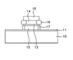
図1は、従来技術により形成されたタングステンゲート電極の断面図であって、これを参照して以下に従来の工程を説明する。
【0005】
従来工程では、まず、シリコン基板10の上にゲート酸化膜11を成長させ、その上にドープしたポリシリコン膜(doped polysilicon)12を蒸着する。次に、ポリシリコン膜12の上に拡散防止膜としてWN膜13及びタングステン膜14を蒸着し、その上にマスク酸化膜15を蒸着する。
【0006】
続いて、マスク酸化膜15及びタングステン膜14、WN膜13及びポリシリコン膜12を順次選択エッチングしてゲート電極をパターニングする。
【0007】
以後、ゲート電極パターニングのためのドライエッチングの際に、ゲート電極及びゲート酸化膜11のエッチング損傷の回復のために、ゲート再酸化(gate re-oxidation)工程を行う。
【0008】
【発明が解決しようとする課題】
このとき、タングステン膜14が高温の酸化雰囲気に露出することで、タングステン膜14の側壁に、揮発性絶縁物質のタングステンオクサイド(WO3)16が形成されて、ゲート電極の形態(morphology)が壊れることになる。このように変形されたゲート電極は、イオン注入工程及び側壁スペーサ形成工程などの後続工程に影響を与えることになり、所望の素子特性を得にくくなる。また、タングステン膜14の酸化がひどい場合、タングステン(W)の量が低減して、ゲート電極の抵抗が増加するという問題点があった。
【0009】
図1の符号17は、ゲート再酸化工程によりポリシリコン膜12側壁に形成された熱酸化膜である。
【0010】
上記の問題点を解決するために、山本(N.Yamamoto)等によりウェット水素酸化(Wet Hydrogen Oxidation)(Journal of Electrochemical Society,Vol.133,p.401(1986)参照)工程が提案されたが、この工程は必要な厚さの熱酸化膜を得る為に、高温(1000℃)で、長時間の酸化工程を行わなければならない。これにより、金属ゲート電極の使用が予想される4GDRAM以上の半導体素子では、莫大な熱量(thermal budget)が要求される。
【0011】
また、かかる問題を避けるために、窒素雰囲気下で熱処理を行う場合、ゲート酸化膜の特性は酸素雰囲気下で熱処理を行う場合に比べて劣化するという問題点があった。
【0012】
従って、本発明の目的は、ゲート再酸化工程の際、所要熱量及びゲート絶縁膜の劣化を増加させることなく、金属の異常酸化現象を防止できる半導体素子のゲート電極形成方法を提供することにある。
【0013】
【課題を解決するための手段】
上記の問題点を解決するために、本発明による半導体素子のゲート電極形成方法は、半導体基板の上にゲート絶縁膜を形成し、前記ゲート絶縁膜の上にポリシリコン膜を形成する段階と、前記ポリシリコン膜の上に拡散防止膜を形成する段階と、前記拡散防止膜の上に、酸化時に導電性金属酸化膜を形成できる金属からなる金属膜を形成する段階と、前記金属膜、前記拡散防止膜及び前記ポリシリコン膜を選択エッチングしてゲート電極パターンを形成する段階と、前記半導体基板の全体構造に対してゲート再酸化工程を行う段階とを含み、前記金属膜は、イリジウム(Ir)、オスミウム(Os)のいずれか一つにより形成され、前記ゲート再酸化を行う段階の際、前記ゲート電極パターンの金属層側壁に均一な導電性金属酸化膜が形成されることを特徴とする。
【0014】
つまり、本発明は、従来のタングステンの様な高融点金属の代わりに、イリジウム(Ir)、オスミウム(Os)などの様に酸化されて非揮発性の導電性金属酸化膜を形成する金属をゲート電極材料として用いる。これにより、通常のゲート再酸化工程を行っても、金属膜の異常酸化現象なしに均一な酸化膜を得ることができ、かつその酸化膜は電導性のため、ゲート電極の抵抗特性を改善することができる。
【0015】
【発明の実施の形態】
次に、本発明にかかる、半導体素子のゲート電極形成方法の実施の形態の具体例を図面を参照しながら説明する。
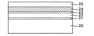
図2乃至図4は、本発明の一実施例によるイリジウムゲート電極形成工程図であって、これを参照して以下に説明する。
【0016】
まず、図2に示すように、シリコン基板20の上にゲート酸化膜21を成長させ、その上にドープしたポリシリコン膜22を500〜1500Å厚さで蒸着する。続いて、その上に拡散防止膜として50〜300Å厚さのWN膜23(またはTiN膜)及び300〜1000Å厚さのイリジウム膜(Ir)24を蒸着し、イリジウム膜24の上にマスク酸化膜25を蒸着する。
【0017】
次に、図3に示すように、マスク酸化膜25、イリジウム膜24、WN膜23及びポリシリコン膜22を選択的にドライエッチングしてゲート電極をパターニングする。このとき、ゲート酸化膜21も僅かにエッチングされる。
【0018】
続いて、図4に示すように、700〜900℃温度のウェットまたはドライ雰囲気下で、通常のゲート再酸化工程を行い、ゲート酸化膜21のエッチング損傷を回復させ、ポリシリコン膜22側壁には熱酸化膜26aを、イリジウム膜24側壁には導電性酸化イリジウム膜(IrO2)26bをそれぞれ30〜150Åの均一な厚さで形成する。前記導電性酸化イリジウム膜(IrO2)26bは、200μΩ・cm以下の比抵抗を持つことにより非常に良好な導電性を持つ。
【0019】
以後、LDD(Lighiy Doped Drain)イオン注入及び側壁スペーサ形成工程を行い、ソース/ドレインのイオン注入を行うことになる。
【0020】
前記の様な工程を行うことにより、ゲート再酸化工程の際、ゲート金属側壁に均一な導電性金属酸化膜が形成されるので、異常酸化現象を防止できる。
【0021】
尚、本発明は本実施例に限られるものではない。例えば、前記実施例では、ゲート金属としてイリジウムを用いる場合を一例にして説明したが、その代わりに、ルテニウム(Ru)、オスミウム(Os)の様に酸化されて導電性金属酸化膜を形成する金属であれば用いても良い。また、その他本発明の趣旨から逸脱しない範囲内で、多様に変形・実施することが可能である。
【0022】
【発明の効果】
以上のように、本発明は、既存のポリシリコンゲートまたはポリサイドゲートの為に、セットアップされたゲート再酸化工程をそのまま使用しても金属膜の異常酸化現象を抑制でき、別の追加工程なしにゲート電極の電気的特性及び工程の安全性を確保することができる。
【図面の簡単な説明】
【図1】従来技術により形成されたタングステンゲート電極の断面図である。
【図2】本発明の一実施例によるイリジウムゲート電極形成工程図である。
【図3】本発明の一実施例によるイリジウムゲート電極形成工程図である。
【図4】本発明の一実施例によるイリジウムゲート電極形成工程図である。
【符号の説明】
20 シリコン基板
21 ゲート酸化膜
22 ドープしたポリシリコン膜
23 WN膜
24 イリジウム膜
25 マスク酸化膜
26a 熱酸化膜
26b 酸化イリジウム膜[0001]
BACKGROUND OF THE INVENTION
The present invention relates to a semiconductor manufacturing technique, and more particularly to a method for forming a gate electrode of a semiconductor element.
[0002]
[Prior art]
In general, the gate electrode of a MOS transistor has been formed using a polysilicon film. The polysilicon gate electrode has an advantage that its formation process is stable. However, with the high integration of semiconductor elements, various patterns including gate electrodes have been miniaturized, and recently, miniaturization has progressed to a line width of 0.15 μm or less. Along with this, doped polysilicon used as a normal gate electrode material has a problem that it is difficult to apply to a device requiring high speed operation due to a long delay time due to its high specific resistance characteristics. .
[0003]
Such a problem becomes a serious problem as the semiconductor device is highly integrated. In order to improve this, a gate electrode technology of a polycide (polycide, polysilicon / silicide) structure using a refractory metal element such as tungsten or titanium has been proposed. However, there is a limit to the improvement of the operation speed of the semiconductor device in which such a polycide structure gate electrode is also highly integrated. Recently, there is a technology using a refractory metal such as tungsten (W) as a gate electrode. It is actively researched and developed.
[0004]
FIG. 1 is a cross-sectional view of a tungsten gate electrode formed by a conventional technique, and a conventional process will be described below with reference to this.
[0005]
In the conventional process, first, a
[0006]
Subsequently, the
[0007]
Thereafter, in dry etching for gate electrode patterning, a gate re-oxidation process is performed to recover etching damage of the gate electrode and the
[0008]
[Problems to be solved by the invention]
At this time, the
[0009]
[0010]
In order to solve the above problems, N. Yamamoto et al. Proposed a wet hydrogen oxidation (see Journal of Electrochemical Society, Vol. 133, p. 401 (1986)) process. In this process, in order to obtain a thermal oxide film having a necessary thickness, an oxidation process for a long time must be performed at a high temperature (1000 ° C.). As a result, an enormous thermal budget is required for a semiconductor device of 4GDRAM or higher where the use of a metal gate electrode is expected.
[0011]
In order to avoid such a problem, when the heat treatment is performed in a nitrogen atmosphere, the characteristics of the gate oxide film are deteriorated as compared with the case where the heat treatment is performed in an oxygen atmosphere.
[0012]
Accordingly, an object of the present invention is to provide a method for forming a gate electrode of a semiconductor device capable of preventing an abnormal oxidation phenomenon of a metal without increasing required heat amount and deterioration of a gate insulating film during a gate reoxidation process. .
[0013]
[Means for Solving the Problems]
In order to solve the above problems, a method of forming a gate electrode of a semiconductor device according to the present invention includes forming a gate insulating film on a semiconductor substrate and forming a polysilicon film on the gate insulating film; Forming a diffusion prevention film on the polysilicon film, forming a metal film made of a metal capable of forming a conductive metal oxide film upon oxidation on the diffusion prevention film, the metal film, A step of selectively etching the diffusion barrier layer and the polysilicon layer to form a gate electrode pattern; and a step of performing a gate reoxidation process on the entire structure of the semiconductor substrate , wherein the metal layer comprises iridium (Ir) ), A uniform conductive metal oxide film is formed on the sidewall of the metal layer of the gate electrode pattern during the gate re-oxidation. Characterized in that that.
[0014]
That is, the present invention gates a metal that forms a non-volatile conductive metal oxide film, such as iridium (Ir) or osmium (Os), instead of a conventional high melting point metal such as tungsten. Used as electrode material. As a result, even if a normal gate re-oxidation process is performed, a uniform oxide film can be obtained without an abnormal oxidation phenomenon of the metal film, and since the oxide film is conductive, the resistance characteristic of the gate electrode is improved. be able to.
[0015]
DETAILED DESCRIPTION OF THE INVENTION
Next, a specific example of an embodiment of a method for forming a gate electrode of a semiconductor element according to the present invention will be described with reference to the drawings.
2 to 4 are iridium gate electrode forming steps according to an embodiment of the present invention, which will be described below with reference to FIG.
[0016]
First, as shown in FIG. 2, a
[0017]
Next, as shown in FIG. 3, the
[0018]
Subsequently, as shown in FIG. 4, a normal gate reoxidation process is performed in a wet or dry atmosphere at a temperature of 700 to 900 ° C. to recover the etching damage of the
[0019]
Thereafter, LDD (Lighiy Doped Drain) ion implantation and sidewall spacer forming steps are performed, and source / drain ion implantation is performed.
[0020]
By performing the process as described above, a uniform conductive metal oxide film is formed on the gate metal side wall during the gate reoxidation process, so that an abnormal oxidation phenomenon can be prevented.
[0021]
The present invention is not limited to this embodiment. For example, in the above embodiment, the case where iridium is used as the gate metal has been described as an example. Instead, a metal that is oxidized like ruthenium (Ru) or osmium (Os) to form a conductive metal oxide film If so, it may be used. In addition, various modifications and implementations can be made without departing from the spirit of the present invention.
[0022]
【The invention's effect】
As described above, the present invention can suppress the abnormal oxidation phenomenon of the metal film even if the set-up gate reoxidation process is used as it is for the existing polysilicon gate or polycide gate, and there is no additional process. In addition, the electrical characteristics of the gate electrode and the process safety can be ensured.
[Brief description of the drawings]
FIG. 1 is a cross-sectional view of a tungsten gate electrode formed by a conventional technique.
FIG. 2 is a process diagram of forming an iridium gate electrode according to an embodiment of the present invention.
FIG. 3 is a process diagram of forming an iridium gate electrode according to an embodiment of the present invention.
FIG. 4 is a process diagram of forming an iridium gate electrode according to an embodiment of the present invention.
[Explanation of symbols]
20
Claims (4)
前記ポリシリコン膜の上に拡散防止膜を形成する段階と、
前記拡散防止膜の上に、酸化時に導電性金属酸化膜を形成できる金属からなる金属膜を形成する段階と、
前記金属膜、前記拡散防止膜及び前記ポリシリコン膜を選択エッチングしてゲート電極パターンを形成する段階と、
前記半導体基板の全体構造に対してゲート再酸化工程を行う段階とを含み、
前記金属膜は、イリジウム(Ir)、オスミウム(Os)のいずれか一つにより形成され、
前記ゲート再酸化を行う段階の際、前記ゲート電極パターンの金属層側壁に均一な導電性金属酸化膜が形成されることを特徴とする半導体素子のゲート電極形成方法。Forming a gate insulating film on the semiconductor substrate and forming a polysilicon film on the gate insulating film;
Forming a diffusion barrier layer on the polysilicon film;
Forming a metal film made of a metal capable of forming a conductive metal oxide film upon oxidation on the diffusion preventing film;
Selectively etching the metal film, the diffusion barrier film and the polysilicon film to form a gate electrode pattern;
Performing a gate reoxidation process on the entire structure of the semiconductor substrate ,
The metal film is formed of any one of iridium (Ir) and osmium (Os),
A method for forming a gate electrode of a semiconductor device , wherein a uniform conductive metal oxide film is formed on a sidewall of the metal layer of the gate electrode pattern during the gate re-oxidation .
Applications Claiming Priority (2)
| Application Number | Priority Date | Filing Date | Title |
|---|---|---|---|
| KR1019980058595A KR100318442B1 (en) | 1998-12-24 | 1998-12-24 | A method for forming metal gate electrode in semiconductor device |
| KR1998/P58595 | 1998-12-24 |
Publications (2)
| Publication Number | Publication Date |
|---|---|
| JP2000196083A JP2000196083A (en) | 2000-07-14 |
| JP3689757B2 true JP3689757B2 (en) | 2005-08-31 |
Family
ID=19565677
Family Applications (1)
| Application Number | Title | Priority Date | Filing Date |
|---|---|---|---|
| JP35270099A Expired - Fee Related JP3689757B2 (en) | 1998-12-24 | 1999-12-13 | Method for forming gate electrode of semiconductor element |
Country Status (4)
| Country | Link |
|---|---|
| US (1) | US6303494B1 (en) |
| JP (1) | JP3689757B2 (en) |
| KR (1) | KR100318442B1 (en) |
| TW (1) | TW432513B (en) |
Families Citing this family (8)
| Publication number | Priority date | Publication date | Assignee | Title |
|---|---|---|---|---|
| KR100313943B1 (en) * | 1999-04-22 | 2001-11-15 | 김영환 | Method for forming gate of semiconductor device |
| JP2000349285A (en) * | 1999-06-04 | 2000-12-15 | Hitachi Ltd | Method of manufacturing semiconductor integrated circuit device and semiconductor integrated circuit device |
| TW434704B (en) * | 1999-06-11 | 2001-05-16 | Univ Nat Yunlin Sci & Tech | Device of amorphous WO3 ion sensitive field effect transistor (ISFET) and method for making the same |
| KR100511897B1 (en) * | 1999-06-24 | 2005-09-02 | 주식회사 하이닉스반도체 | method of forming gate electrode of semiconductor device |
| US6830975B2 (en) * | 2002-01-31 | 2004-12-14 | Micron Technology, Inc. | Method of forming field effect transistor comprising at least one of a conductive metal or metal compound in electrical connection with transistor gate semiconductor material |
| JP4622213B2 (en) * | 2003-07-04 | 2011-02-02 | 株式会社日立製作所 | Semiconductor device |
| KR100596802B1 (en) * | 2005-05-27 | 2006-07-04 | 주식회사 하이닉스반도체 | Manufacturing method of semiconductor device |
| JP2007073637A (en) * | 2005-09-05 | 2007-03-22 | Tokyo Electron Ltd | Film-forming method and semiconductor device manufacturing method |
Family Cites Families (12)
| Publication number | Priority date | Publication date | Assignee | Title |
|---|---|---|---|---|
| JPS5979573A (en) | 1982-10-29 | 1984-05-08 | Hitachi Ltd | semiconductor equipment |
| US4839700A (en) | 1987-12-16 | 1989-06-13 | California Institute Of Technology | Solid-state non-volatile electronically programmable reversible variable resistance device |
| JPH022134A (en) | 1988-06-15 | 1990-01-08 | Toshiba Corp | Insulation gate type transistor |
| US5264380A (en) | 1989-12-18 | 1993-11-23 | Motorola, Inc. | Method of making an MOS transistor having improved transconductance and short channel characteristics |
| JPH03286569A (en) | 1990-04-03 | 1991-12-17 | Nec Corp | Mes-type field-effect transistor |
| JPH0548095A (en) | 1991-08-07 | 1993-02-26 | Canon Inc | Semiconductor device and manufacturing method thereof |
| JPH09246490A (en) * | 1996-03-11 | 1997-09-19 | Toshiba Corp | Semiconductor device and manufacturing method thereof |
| US5723893A (en) | 1996-05-28 | 1998-03-03 | Taiwan Semiconductor Manufacturing Company, Ltd. | Method for fabricating double silicide gate electrode structures on CMOS-field effect transistors |
| DE19623517C1 (en) | 1996-06-12 | 1997-08-21 | Siemens Ag | MOS transistors for biotechnical applications |
| JP3454058B2 (en) | 1996-12-11 | 2003-10-06 | 富士通株式会社 | Semiconductor memory and manufacturing method thereof |
| JPH10294431A (en) * | 1997-04-18 | 1998-11-04 | Oki Electric Ind Co Ltd | Semiconductor storage element and its manufacture |
| US5907780A (en) | 1998-06-17 | 1999-05-25 | Advanced Micro Devices, Inc. | Incorporating silicon atoms into a metal oxide gate dielectric using gas cluster ion beam implantation |
-
1998
- 1998-12-24 KR KR1019980058595A patent/KR100318442B1/en not_active Expired - Fee Related
-
1999
- 1999-12-07 TW TW088121363A patent/TW432513B/en not_active IP Right Cessation
- 1999-12-13 JP JP35270099A patent/JP3689757B2/en not_active Expired - Fee Related
- 1999-12-14 US US09/460,815 patent/US6303494B1/en not_active Expired - Fee Related
Also Published As
| Publication number | Publication date |
|---|---|
| US6303494B1 (en) | 2001-10-16 |
| KR20000042430A (en) | 2000-07-15 |
| JP2000196083A (en) | 2000-07-14 |
| TW432513B (en) | 2001-05-01 |
| KR100318442B1 (en) | 2002-02-19 |
Similar Documents
| Publication | Publication Date | Title |
|---|---|---|
| JP4484392B2 (en) | Method for forming gate electrode of semiconductor element | |
| JP3406265B2 (en) | Semiconductor device and manufacturing method thereof | |
| JP3689757B2 (en) | Method for forming gate electrode of semiconductor element | |
| US6218252B1 (en) | Method of forming gate in semiconductor device | |
| JP2738371B2 (en) | Method for manufacturing semiconductor device | |
| KR100296140B1 (en) | Gate electrode formation method of semiconductor device | |
| KR100819685B1 (en) | Manufacturing method of semiconductor device | |
| JP4424652B2 (en) | Method for forming gate electrode of semiconductor element | |
| JP2003158196A (en) | Semiconductor device and method of manufacturing the same | |
| KR19980060621A (en) | Manufacturing method of semiconductor device | |
| KR100353525B1 (en) | Method for forming gate electrode in semiconductor device | |
| KR20020013195A (en) | Method for forming gate pattern of semiconductor device | |
| KR100365409B1 (en) | Method for forming a gate electrode in semiconductor device | |
| KR100335274B1 (en) | Manufacturing method of semiconductor device | |
| KR20040059931A (en) | Method for fabricating dual gate oxide of semiconductor device | |
| KR100265348B1 (en) | Method for fabricating mosfet having polycide gate | |
| KR100806135B1 (en) | Method for manufacturing a semiconductor device having a metal gate electrode | |
| KR100465855B1 (en) | Gate electrode formation method of semiconductor device | |
| KR100543654B1 (en) | Gate Forming Method of Semiconductor Device | |
| TW558759B (en) | Method of forming and etching resistor protection oxide layer | |
| KR100265349B1 (en) | Method for fabricating mosfet having polycide gate | |
| KR20000061321A (en) | Manufacturing method for mos transistor | |
| KR100693878B1 (en) | Semiconductor device having low resistance and manufacturing method thereof | |
| KR100403355B1 (en) | Manufacturing method of semiconductor device | |
| KR20040036960A (en) | Semiconductor and fabricating method of it |
Legal Events
| Date | Code | Title | Description |
|---|---|---|---|
| A977 | Report on retrieval |
Free format text: JAPANESE INTERMEDIATE CODE: A971007 Effective date: 20041221 |
|
| A131 | Notification of reasons for refusal |
Free format text: JAPANESE INTERMEDIATE CODE: A131 Effective date: 20050104 |
|
| A521 | Request for written amendment filed |
Free format text: JAPANESE INTERMEDIATE CODE: A523 Effective date: 20050404 |
|
| RD02 | Notification of acceptance of power of attorney |
Free format text: JAPANESE INTERMEDIATE CODE: A7422 Effective date: 20050404 |
|
| TRDD | Decision of grant or rejection written | ||
| A01 | Written decision to grant a patent or to grant a registration (utility model) |
Free format text: JAPANESE INTERMEDIATE CODE: A01 Effective date: 20050510 |
|
| A61 | First payment of annual fees (during grant procedure) |
Free format text: JAPANESE INTERMEDIATE CODE: A61 Effective date: 20050524 |
|
| R150 | Certificate of patent or registration of utility model |
Free format text: JAPANESE INTERMEDIATE CODE: R150 |
|
| FPAY | Renewal fee payment (event date is renewal date of database) |
Free format text: PAYMENT UNTIL: 20080624 Year of fee payment: 3 |
|
| FPAY | Renewal fee payment (event date is renewal date of database) |
Free format text: PAYMENT UNTIL: 20090624 Year of fee payment: 4 |
|
| FPAY | Renewal fee payment (event date is renewal date of database) |
Free format text: PAYMENT UNTIL: 20100624 Year of fee payment: 5 |
|
| FPAY | Renewal fee payment (event date is renewal date of database) |
Free format text: PAYMENT UNTIL: 20110624 Year of fee payment: 6 |
|
| FPAY | Renewal fee payment (event date is renewal date of database) |
Free format text: PAYMENT UNTIL: 20120624 Year of fee payment: 7 |
|
| FPAY | Renewal fee payment (event date is renewal date of database) |
Free format text: PAYMENT UNTIL: 20130624 Year of fee payment: 8 |
|
| LAPS | Cancellation because of no payment of annual fees |