JP3678437B2 - Method for manufacturing liquid crystal display device and liquid crystal display device - Google Patents
Method for manufacturing liquid crystal display device and liquid crystal display device Download PDFInfo
- Publication number
- JP3678437B2 JP3678437B2 JP4559694A JP4559694A JP3678437B2 JP 3678437 B2 JP3678437 B2 JP 3678437B2 JP 4559694 A JP4559694 A JP 4559694A JP 4559694 A JP4559694 A JP 4559694A JP 3678437 B2 JP3678437 B2 JP 3678437B2
- Authority
- JP
- Japan
- Prior art keywords
- thin film
- film transistor
- gate electrode
- region
- conductivity type
- Prior art date
- Legal status (The legal status is an assumption and is not a legal conclusion. Google has not performed a legal analysis and makes no representation as to the accuracy of the status listed.)
- Expired - Lifetime
Links
Images


Classifications
-
- H—ELECTRICITY
- H01—ELECTRIC ELEMENTS
- H01L—SEMICONDUCTOR DEVICES NOT COVERED BY CLASS H10
- H01L27/00—Devices consisting of a plurality of semiconductor or other solid-state components formed in or on a common substrate
- H01L27/02—Devices consisting of a plurality of semiconductor or other solid-state components formed in or on a common substrate including semiconductor components specially adapted for rectifying, oscillating, amplifying or switching and having at least one potential-jump barrier or surface barrier; including integrated passive circuit elements with at least one potential-jump barrier or surface barrier
- H01L27/12—Devices consisting of a plurality of semiconductor or other solid-state components formed in or on a common substrate including semiconductor components specially adapted for rectifying, oscillating, amplifying or switching and having at least one potential-jump barrier or surface barrier; including integrated passive circuit elements with at least one potential-jump barrier or surface barrier the substrate being other than a semiconductor body, e.g. an insulating body
- H01L27/1214—Devices consisting of a plurality of semiconductor or other solid-state components formed in or on a common substrate including semiconductor components specially adapted for rectifying, oscillating, amplifying or switching and having at least one potential-jump barrier or surface barrier; including integrated passive circuit elements with at least one potential-jump barrier or surface barrier the substrate being other than a semiconductor body, e.g. an insulating body comprising a plurality of TFTs formed on a non-semiconducting substrate, e.g. driving circuits for AMLCDs
- H01L27/1259—Multistep manufacturing methods
- H01L27/1288—Multistep manufacturing methods employing particular masking sequences or specially adapted masks, e.g. half-tone mask
-
- H—ELECTRICITY
- H01—ELECTRIC ELEMENTS
- H01L—SEMICONDUCTOR DEVICES NOT COVERED BY CLASS H10
- H01L27/00—Devices consisting of a plurality of semiconductor or other solid-state components formed in or on a common substrate
- H01L27/02—Devices consisting of a plurality of semiconductor or other solid-state components formed in or on a common substrate including semiconductor components specially adapted for rectifying, oscillating, amplifying or switching and having at least one potential-jump barrier or surface barrier; including integrated passive circuit elements with at least one potential-jump barrier or surface barrier
- H01L27/12—Devices consisting of a plurality of semiconductor or other solid-state components formed in or on a common substrate including semiconductor components specially adapted for rectifying, oscillating, amplifying or switching and having at least one potential-jump barrier or surface barrier; including integrated passive circuit elements with at least one potential-jump barrier or surface barrier the substrate being other than a semiconductor body, e.g. an insulating body
- H01L27/1214—Devices consisting of a plurality of semiconductor or other solid-state components formed in or on a common substrate including semiconductor components specially adapted for rectifying, oscillating, amplifying or switching and having at least one potential-jump barrier or surface barrier; including integrated passive circuit elements with at least one potential-jump barrier or surface barrier the substrate being other than a semiconductor body, e.g. an insulating body comprising a plurality of TFTs formed on a non-semiconducting substrate, e.g. driving circuits for AMLCDs
Description
【0001】
【産業上の利用分野】
本発明は、液晶表示基板の製造方法に係り、いわゆるアクティブ・マトリックス方式と称され、各画素に対応して薄膜スイッチング素子(TFT)を備えた液晶表示基板の製造方法に関する。
【0002】
【従来の技術】
上述した薄膜スイッチング素子を備える液晶表示基板は、マトリックス状に配置された各画素のうち、所定の列方向に配列された各画素に対応する薄膜スイッチング素子を全てオンするとともに、このオンされた薄膜スイッチング素子を介して各画素に映像信号に対応する電圧を印加するようになっている。
【0003】
そして、薄膜スイッチング素子は、透明基板面に形成された島状のたとえばポリSiからなる半導体層を覆うようにして絶縁膜を形成し、さらに、この絶縁膜上に前記半導体層を分断するようにゲート電極を形成し、該ゲート電極をマスクとした不純物のイオン打ち込みでソースおよびドレインの各領域を形成する(セルフ・アライメント)ことによって得られるMOS型トランジスタを構成している。
【0004】
この場合、列方向に配列された各薄膜スイッチング素子のゲート電極は共通接続されて走査信号線を構成し、行方向に配列された各薄膜スイッチング素子のドレイン電極は共通接続されて映像信号線を構成している。
【0005】
【発明が解決しようとする課題】
しかしながら、このように構成された液晶表示基板において、その薄膜スイッチング素子は、上述したようにゲート電極をマスクとした不純物イオン打ち込みによってソースおよびドレインの各領域を形成していることから、ゲート電極のチャンネル長に対応する端辺の直下に前記各領域の端辺が位置づけられて形成されてしまうことになる。
【0006】
このため、薄膜スイッチング素子をオンからオフにした段階で、画素電極側に充電された電荷がソースに対して負電位となったゲート電極を介してドレイン側になだれ現象を起こしてしまうことになる(Drain induced Break down)。
【0007】
この弊害を除くためにはゲート電極に対してソースあるいはドレインの各領域をオフセット構造にすることが考えられるが、製造工数を増大させてしまうという問題が残されることになる。
【0008】
それ故、本発明はこのような事情に基づいてなされたものであり、その目的とするところのものは、従来の製造工数を全く増大することなく、表示領域内に形成されている薄膜トランジスタ素子のドレインが引き起こすブレイクダウンの発生を防止できる液晶表示基板の製造方法を提供することにある。
【0009】
【課題を解決するための手段】
このような目的を達成するために、本発明は、基本的には、一方の透明基板の面に表示領域とそれ以外の領域を有し、前記表示領域にはその各画素に対応したMOS型トランジスタ(薄膜トランジスタ素子:以下、この明細書において表示領域内のみに形成されているトランジスタを薄膜トランジスタと称する)が形成されているとともに液晶を介して他方の透明基板が対向配置され、前記表示領域以外の領域にはコンプリメンタリMOS型トランジスタを含む回路が形成されている液晶表示基板において、前記表示領域の薄膜トランジスタ素子のソースおよびドレインの各領域をそのゲート電極をマスクとして不純物の打ち込みで形成する際に、前記表示領域以外の領域のコンプリメンタリMOS型トランジスタのうちの一方のMOS型トランジスタを覆って形成するマスクと同一かつ同工程で少なくとも前記ゲート電極のチャンネル長に対応する辺部を覆ってマスクを形成した後に、前記不純物の打ち込みで前記ソースおよびドレインの各領域を形成することを特徴とするものである。
【0010】
【作用】
このように構成した液晶表示基板の製造方法によれば、ゲート電極のチャンネル長に対応する辺部を覆ってマスクを形成した後に不純物の打ち込みをおこなっていることから、これによって形成されるソースおよびドレインの各領域はゲート電極に対してオフセット構造となる。これにより、薄膜トランジスタ素子のドレインが引き起こすブレイクダウンの発生を防止できるようになる。
【0011】
そして、前記マスクは表示領域以外の領域において形成過程にあるコンプリメンタルMOS型トランジスタのうちの一方のMOS型トランジスタ(薄膜トランジスタと異なる導電型のトランジスタ)を覆わなければならないマスクと同一のものを同工程でそのまま適用させることから製造工程の増大を伴うことがなくなる。
【0012】
【実施例】
以下、本発明が適用される液晶表示基板の一実施例を図6ないし図8を用いて説明する。
【0013】
まず、図6において、図6(a)には液晶表示基板100の平面図を示している。この液晶表示基板100はその周辺部を除く中央部が表示領域(PIXEL AREA)となっている。この表示領域は下ガラス基板に液晶を介して上ガラス基板が対向して配置された領域で、マトリックス状に配置された画素(PIXEL)を構成するようになっている。
【0014】
そして、この表示領域の図中左右両側の下ガラス基板面には垂直走査回路Vが形成されている。
【0015】
この垂直走査回路Vは、図6(b)に示すように、多数のインバータ回路を含む回路から構成され、また、これらインバータ回路は図示していないがコンプリメンタリMOS型トランジスタから構成されている。
【0016】
この垂直走査回路Vの各出力はゲート信号線GLを介して表示領域(PIXEL AREA)内に送出されるようになっている。このゲート信号線GLは該表示領域内の下ガラス基板面に列(X)方向に延在しかつ行(Y)方向に並設される複数の信号線からなっている。
【0017】
また図中、表示領域(PIXEL AREA)の下側の表示領域外の下ガラス基板には映像信号駆動回路Hが形成されている。
【0018】
この映像信号駆動回路Hは、図7(a)に示すように、多数のインバータ回路を含む回路から構成され、また、これらインバータ回路は図示していないがコンプリメンタリMOS型トランジスタから構成されている。なお、図7(a)に示す液晶表示基板は図6(a)に示すそれと同じものである。
【0019】
この映像信号駆動回路Hの各出力はドレイン信号線DLを介して表示領域(PIXEL AREA)内に送出されるようになっている。このドレイン信号線DLは該表示領域内の下ガラス基板面に行(Y)方向に延在しかつ列(X)方向に並設される複数の信号線からなっている。
【0020】
図8(a)は、前記表示領域(PIXEL AREA)内の構成の一部を示したものである。他の部分においても同様のパターンで構成されたものとなっている。
【0021】
同図において、互いに直交して並設されるゲート信号線GLとドレイン信号線DLで囲まれる各領域が画素領域となり、この画素領域にはたとえばITO(Indium-Tin-Oxide)からなる画素電極CLcが形成されている。そして、この画素電極CLcの近傍には薄膜トランジスタ素子(TFT)が形成され、この薄膜トランジスタ素子(TFT)を介して該画素電極CLcはドレイン信号線DLに接続されている。
【0022】
薄膜トランジスタ素子(TFT)のゲート電極は前記ゲート信号線GLの一部を用いて形成されている。
【0023】
これにより、ゲート信号線GLに信号が入力されると、薄膜トランジスタ素子(TFT)がオン状態になり、この薄膜トランジスタ素子(TFT)を介してドレイン信号線DLから映像信号に対応する電圧が画素電極CLcに印加されることになる。
【0024】
画素電極CLcは液晶を介して図示しない共通電極(上ガラス基板側に形成されている)との間に電界を構成し、この電界によって該液晶の透光度合いを変化させるようになっている。
【0025】
なお、この画素電極CLcは、その近傍に形成された保持容量素子(Cst)に接続されている。この保持容量素子(Cst)は、たとえば、薄膜トランジスタ(TFT)がオフ状態となった後の映像信号を長く蓄積させる等の目的で形成されたものである。
【0026】
図8の実施例では保持容量素子Cstが画素電極CLcに接続されない側の電極を介して容量線に接続され、たとえば共通電極と同等の電圧が印加される。
【0027】
図8(b)は同図(a)の等価回路を示すものである。
【0028】
次に、このような構成からなる表示基板の製造方法の一実施例を図1ないし図4を用いてステップ毎に説明する。なお、各図において、図中左側は表示領域内に形成される薄膜トランジスタ素子(TFT)の形成領域を、また、図中右側は表示領域以外の領域内に形成されるコンプリメンタリMOS型トランジスタの形成領域を示している。また、前記薄膜トランジスタ素子(TFT)の製造方法は、図8のI−I線における断面図に基づいて説明する。
また、図2から図4では薄膜トランジスタ(TFT)の製造方法に加えて、保持容量素子(Cst)の製造方法についても示している。ただし、図が複雑になることを避けるために、薄膜トランジスタ(TFT)と保持容量素子(Cst)の位置関係は実際のものとは異なり模式的に記載してある。
【0029】
ステップ1.(図1(a))
主表面が充分に洗浄されたガラス基板を用意する。
【0030】
ステップ2.(図1(b))
ガラス基板の主表面の全域にたとえばディポジション法によってポリシリコン(poly-Si)層2を形成する。
【0031】
ステップ3.(図1(c))
該ポリシリコン層2を選択エッチングする。この選択エッチングにより、該ポリシリコン層2は表示領域における薄膜トランジスタ(TFT)および保持容量素子(Cst)の形成領域に、表示領域以外の領域におけるスイッチング素子(特に、コンプリメンタリMOSトランジスタ)の形成領域に残存させるようにする。
【0032】
ステップ4.(図1(d))
残存されたポリシリコン層2の表面に熱酸化処理を施すことにより、シリコン酸化膜3を形成する。このシリコン酸化膜3は後に形成される薄膜トランジスタ(TFT)等のゲート酸化膜となるものである。
【0033】
ステップ5.(図1(e))
このように加工された主表面の全域にフォトレジスト膜4を塗布し、その選択除去により前記保持容量素子(Cst)の形成領域を露呈させる。
【0034】
その後、イオン打ち込み方法を用いて高濃度のN型不純物をドープして、該保持容量(Cst)の形成領域におけるポリシリコン層2を導電化させる。この導電化されたポリシリコン層2は後に形成される保持容量素子(Cst)の一方の電極となるものである。
【0035】
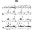
ステップ6.(図2(a))
残存されている前記フォトレジスト膜4を除去し、リン(P)処理されたポリシリコン(poly-Si)層5をたとえばディポジション方法を用いて全域に形成する。
【0036】
ステップ7.(図2(b))
前記ポリシリコン(Poly-Si)層5を選択エッチングし、これにより薄膜トランジスタ(TFT)、コンプリメンタリMOS型トランジスタの各ゲート電極を形成するとともに、保持容量素子(Cst)を形成する。
【0037】
ステップ8.(図2(c))
そして、残存されているポリシリコン(poly-Si)層5をマスクとして、このポリシリコン(poly-Si)層5から露呈されている前記シリコン酸化膜3をエッチングする。
【0038】
前記シリコン酸化膜3のエッチングにより露呈されたポリシリコン(poly-Si)層2、およびゲート電極等として形成されているポリシリコン(poly-Si)5層を軽く熱酸化することにより、それらの表面にシリコン酸化膜を形成する。
【0039】
ステップ9.(図2(d))
コンプリメンタリMOS型トランジスタのうちP型のMOS型トランジスタの全域を覆ってフォトレジスト7を形成する。なお、該P型のMOS型トランジスタは薄膜トランジスタ素子(TFT)と異なる導電型を有するトランジスタである。
【0040】
ここで、この実施例では、特に、同工程で薄膜トランジスタ(TFT)のゲート電極を覆ってフォトレジスト7Aを形成する。
【0041】
すなわち、全域に形成したフォトレジスト7を選択除去する際に、コンプリメンタリMOS型トランジスタのうちP型のMOS型トランジスタの上面に形成されているフォトレジスト、および薄膜トランジスタ(TFT)のゲート電極の上面に形成されているフォトレジスト(符号7Aで示す)を残存させて他のフォトレジストを除去する。
【0042】
この場合、薄膜トランジスタ素子(TFT)側に残存させるフォトレジスト7Aは少なくともゲート電極のチャンネル長方向の辺の側壁を覆うように形成することが必須となる。
【0043】
その後、このように加工された表面の全域に高濃度のN型不純物をイオン打ち込み方法を用いて高濃度のN型不純物をドープする。
【0044】
これにより、薄膜トランジスタ(TFT)のソースS、ドレインDの各領域、およびコンプリメンタリMOS型トランジスタのうちN型のMOS型トランジスタのソースS、ドレインDの各領域が形成されるようになる。
【0045】
ここで、薄膜トランジスタ素子(TFT)のソースS、ドレインDの各領域は、図5に詳細に示すように、ゲート電極のチャンネル長方向の辺の直下からlの距離を隔ててソースSおよびドレインDの領域の端辺が位置づけられることになる。
【0046】
これにより、ソースSおよびドレインDの各領域はゲート電極(符号5で示す)に対してオフセットされた構造で形成されることになる。
【0047】
ステップ10.(図3(a))
残存されているフォトレジスト7を除去し、さらに新たなフォトレシジスト8を全域に形成した後にこのフォトレジスト8を選択除去する。この選択除去によって、コンプリメンタリMOS型トランジスタのうちP型のMOS型トランジスタのみを露呈させる。
【0048】
その後、フッ化ボロン(BF2)からなるP型不純物をイオン打ち込み方法によりドープし、これにより該MOS型トランジスタのソースS、ドレインDの各領域を形成する。
【0049】
ステップ11.(図3(b))
残存しているフォトレジスト8を除去し、たとえば気相成長法によってシリコン酸化膜およびリンシリケートガラスを順次形成して、2層構造の絶縁膜9を形成する。
【0050】
ステップ12.(図3(c))
絶縁膜9を選択エッチングする。この選択エッチングは、薄膜トランジスタ(TFT)のドレイン領域の一部、コンプリメンタリMOS型トランジスタのそれぞれのトランジスタのソース、ドレイン領域の各一部を露呈させるためのコンタクトホールCHを形成するためになされる。
【0051】
ステップ13.(図3(d))
コンタクトホールCHの形成部分を含んで絶縁膜9の全域にアルミニゥム膜10を形成する。
【0052】
ステップ14.(図4(a))
アルミニュム膜10を選択エッチングし、この選択エッチングにより前記コンタクトホールCHにおいて接続部を有する配線層が形成される。
【0053】
ステップ15.(図4(b))
このように配線層が形成された表面の全域にシリコン酸化膜からなる絶縁膜11を形成する。
【0054】
その後、画素領域およびその周辺に相当する領域部の絶縁膜11選択エッチングによって除去する。
【0055】
ステップ16.(図4(c))
画素領域となる部分に相当する一層目の絶縁膜9を選択エッチングし、この絶縁膜の下層に位置づけられるポリシリコン(poly-Si)層2を露呈させる。
【0056】
ステップ17.(図4(d))
このように加工された表面全域にITOからなる透明導電膜を形成し、この透明導電膜を選択エッチングすることにより前記画素領域およびその周辺における透明導電膜を残存させ、これを画素電極12とする。
【0057】
このような実施例に示すような液晶表示基板の製造方法によれば、ゲート電極の少なくともチャンネル長に対応する辺部を覆ってマスク(図2(d)の符号7Aに相当する)を形成した後に不純物の打ち込みをおこなっていることから、これによって形成されるソースSおよびドレインDの各領域はゲート電極に対してオフセット構造となる。これにより、薄膜トランジスタ素子(TFT)のドレインが引き起こすブレイクダウンの発生を防止できるようになる。
【0058】
図9(a)はこのようにして形成されたN型薄膜トランジスタ素子の特性を従来のものと比較して示したものであり、図中点線は従来の特性、実線は本実施例による特性を示したものである。
【0059】
同図から明らかなように、ゲート電位が負の場合にドレイン電流が流れていないことが判明する。
【0060】
なお、図9(b)はP型の薄膜トランジスタ素子(TFT)を形成する場合においても同様な効果を奏することを示したものである。
【0061】
以上示したことから明らかなように、本実施例による液晶表示基板の製造方法によれば、ゲート電極の少なくともチャンネル長に対応する辺部を覆ってマスクを形成した後に不純物の打ち込みをおこなっていることから、これによって形成されるソースおよびドレインの各領域はゲート電極に対してオフセット構造となる。これにより、薄膜トランジスタ素子のドレインが引き起こすブレイクダウンの発生を防止できるようになる。
【0062】
そして、前記マスクは表示領域以外の領域において形成過程にあるコンプリメンタリMOS型トランジスタのうちの一方のMOS型トランジスタ(薄膜トランジスタと異なる導電型のトランジスタ)を覆わなければならないマスクと同一のものを同工程でそのまま適用させることから製造工程の増大を伴うことがなくなる。
【0063】
なお、上述した液晶表示基板は図8に示したように薄膜トランジスタ素子が一画素に対して一個のものについて説明したものであるが、これに限らず、図10に示すように二個備えたものにあっても適用できることはいうまでもない。
【0064】
また、図10に示す実施例によれば、画素電極CLcに接続される保持容量素子Caddの画素電極CLcに接続されない側の電極を介して隣の画素のゲート信号線に接続されるので、図8に示す実施例と異なって、容量線が不要となる。従って、図10の実施例では、容量線がなくなった分、開口率が広がり、製造工程が簡略化される等の効果を有する。
【0065】
【発明の効果】
以上説明したことから明らかなように、本発明による液晶表示基板の製造方法によれば、従来の製造工数を全く増大することなく、表示領域内に形成されている薄膜トランジスタ素子のドレインが引き起こすブレイクダウンの発生を防止できるようになる。
【図面の簡単な説明】
【図1】(a)ないし(e)は、本発明による液晶表示基板の製造方法の一実施例を示す第一図である。
【図2】(a)ないし(d)は、本発明による液晶表示基板の製造方法の一実施例を示す第二図である。
【図3】(a)ないし(d)は、本発明による液晶表示基板の製造方法の一実施例を示す第三図である。
【図4】(a)ないし(d)は、本発明による液晶表示基板の製造方法の一実施例を示す第四図である。
【図5】本発明による液晶表示基板の製造方法の詳細を示す説明図である。
【図6】本発明が適用される液晶表示基板の表示領域外に形成される回路を示した図である。
【図7】本発明が適用される液晶表示基板の表示領域外に形成される回路を示した図である。
【図8】本発明が適用される液晶表示基板の表示領域内に形成される回路を示した図である。
【図9】本発明による液晶表示基板の製造方法の効果を示す説明図である。
【図10】本発明による液晶表示基板の製造方法の他の実施例を示す説明図である。
【符号の説明】
TFT 薄膜トランジスタ素子
7、7A フォトレジスト
S ソース領域
D ドレイン領域[0001]
[Industrial application fields]
The present invention relates to a manufacturing method of a liquid crystal display substrate, which is called a so-called active matrix method, and relates to a manufacturing method of a liquid crystal display substrate provided with a thin film switching element (TFT) corresponding to each pixel.
[0002]
[Prior art]
The liquid crystal display substrate provided with the thin film switching element described above turns on all the thin film switching elements corresponding to the pixels arranged in a predetermined column direction among the pixels arranged in a matrix, and the turned thin film A voltage corresponding to the video signal is applied to each pixel via the switching element.
[0003]
The thin film switching element forms an insulating film so as to cover an island-shaped semiconductor layer made of, for example, poly-Si formed on the transparent substrate surface, and further divides the semiconductor layer on the insulating film. A MOS transistor obtained by forming a gate electrode and forming source and drain regions by ion implantation of impurities using the gate electrode as a mask (self-alignment) is formed.
[0004]
In this case, the gate electrodes of the thin film switching elements arranged in the column direction are commonly connected to form a scanning signal line, and the drain electrodes of the thin film switching elements arranged in the row direction are commonly connected to connect the video signal line. It is composed.
[0005]
[Problems to be solved by the invention]
However, in the liquid crystal display substrate configured in this way, the thin film switching element forms the source and drain regions by impurity ion implantation using the gate electrode as a mask as described above. The edge of each region is positioned and formed immediately below the edge corresponding to the channel length .
[0006]
For this reason, when the thin film switching element is turned off from on, the charge charged on the pixel electrode side causes an avalanche phenomenon on the drain side through the gate electrode having a negative potential with respect to the source. (Drain induced Break down).
[0007]
In order to eliminate this adverse effect, it is conceivable that the source or drain regions are offset with respect to the gate electrode, but the problem of increasing the number of manufacturing steps remains.
[0008]
Therefore, the present invention has been made based on such circumstances, and the object of the present invention is the thin film transistor element formed in the display region without increasing the number of conventional manufacturing steps. An object of the present invention is to provide a method of manufacturing a liquid crystal display substrate that can prevent breakdown caused by a drain.
[0009]
[Means for Solving the Problems]
In order to achieve such an object, the present invention basically has a display area and other areas on the surface of one transparent substrate, and the display area is a MOS type corresponding to each pixel. A transistor (thin film transistor element: hereinafter, a transistor formed only in the display region is referred to as a thin film transistor) is formed, and the other transparent substrate is disposed to face the liquid crystal so that the region other than the display region is disposed. In the liquid crystal display substrate in which a circuit including a complementary MOS transistor is formed in the region, when the source and drain regions of the thin film transistor element in the display region are formed by implanting impurities using the gate electrode as a mask, One of the complementary MOS transistors in the area other than the display area is the MOS transistor. After forming a mask covering at least the sides corresponding to the tea down channel length of the gate electrode with the mask and the same and the same step of forming over the Njisuta, forming each region of the source and drain in implantation of the impurity It is characterized by doing.
[0010]
[Action]
According to the manufacturing method of the liquid crystal display substrate configured as described above, since the impurity is implanted after forming the mask covering the side corresponding to the channel length of the gate electrode, the source formed thereby and Each drain region has an offset structure with respect to the gate electrode. As a result, breakdown caused by the drain of the thin film transistor element can be prevented.
[0011]
The mask is the same as the mask that must cover one of the complementary MOS transistors in the formation process other than the display region (a transistor having a different conductivity type from the thin film transistor). Therefore, the manufacturing process is not increased.
[0012]
【Example】
Hereinafter, an embodiment of a liquid crystal display substrate to which the present invention is applied will be described with reference to FIGS.
[0013]
First, in FIG. 6, FIG. 6A shows a plan view of the liquid
[0014]
A vertical scanning circuit V is formed on the lower glass substrate surface on both the left and right sides of the display area.
[0015]
As shown in FIG. 6B, the vertical scanning circuit V is composed of a circuit including a large number of inverter circuits, and these inverter circuits are composed of complementary MOS transistors although not shown.
[0016]
Each output of the vertical scanning circuit V is sent into the display area ( PIXEL AREA) via the gate signal line GL. The gate signal line GL includes a plurality of signal lines extending in the column (X) direction and arranged in parallel in the row (Y) direction on the lower glass substrate surface in the display region.
[0017]
In the figure, a video signal driving circuit H is formed on the lower glass substrate outside the display area below the display area (PI XE L AREA).
[0018]
As shown in FIG. 7A, the video signal driving circuit H is composed of a circuit including a large number of inverter circuits, and these inverter circuits are composed of complementary MOS type transistors (not shown). Note that the liquid crystal display substrate shown in FIG. 7A is the same as that shown in FIG.
[0019]
Each output of the video signal driving circuit H is sent into the display area ( PIXEL AREA) via the drain signal line DL. The drain signal line DL includes a plurality of signal lines that extend in the row (Y) direction and are arranged in parallel in the column (X) direction on the lower glass substrate surface in the display region.
[0020]
FIG. 8A shows a part of the configuration in the display area (PI XE L AREA). The other parts are also configured in the same pattern.
[0021]
In the figure, each region surrounded by the gate signal line GL and the drain signal line DL that are arranged in parallel with each other is a pixel region. The pixel region includes a pixel electrode CLc made of, for example, ITO (Indium-Tin-Oxide). Is formed. A thin film transistor element (TFT) is formed in the vicinity of the pixel electrode CLc, and the pixel electrode CLc is connected to the drain signal line DL via the thin film transistor element (TFT).
[0022]
A gate electrode of a thin film transistor element (TFT) is formed using a part of the gate signal line GL.
[0023]
Accordingly, when a signal is input to the gate signal line GL, the thin film transistor element (TFT) is turned on, and a voltage corresponding to the video signal is output from the drain signal line DL through the thin film transistor element (TFT) to the pixel electrode CLc. Will be applied.
[0024]
The pixel electrode CLc forms an electric field between the pixel electrode CLc and a common electrode (not shown) (formed on the upper glass substrate side) via a liquid crystal, and the translucency of the liquid crystal is changed by the electric field.
[0025]
The pixel electrode CLc is connected to a storage capacitor element (Cst) formed in the vicinity thereof. The storage capacitor element (Cst) is formed, for example, for the purpose of accumulating a video signal after the thin film transistor (TFT) is turned off.
[0026]
In the embodiment of FIG. 8, the storage capacitor element Cst is connected to the capacitor line via an electrode not connected to the pixel electrode CLc, and for example, a voltage equivalent to the common electrode is applied.
[0027]
FIG. 8B shows an equivalent circuit of FIG.
[0028]
Next, an embodiment of a method for manufacturing a display substrate having such a configuration will be described step by step with reference to FIGS. In each figure, the left side in the figure is a formation area of a thin film transistor element (TFT) formed in the display area, and the right side in the figure is a formation area of a complementary MOS transistor formed in an area other than the display area. Is shown. In addition, a method for manufacturing the thin film transistor element (TFT) will be described based on a cross-sectional view taken along line II in FIG.
2 to 4 also show a method for manufacturing a storage capacitor element (Cst) in addition to a method for manufacturing a thin film transistor (TFT). However, in order to avoid complication of the drawing, the positional relationship between the thin film transistor (TFT) and the storage capacitor element (Cst) is schematically shown unlike the actual one.
[0029]
A glass substrate whose main surface is sufficiently cleaned is prepared.
[0030]
A polysilicon (poly-Si)
[0031]
The
[0032]
Step 4. (Fig. 1 (d))
The surface of the remaining
[0033]
The photoresist film 4 is applied to the entire area of the main surface thus processed, and the formation region of the storage capacitor element (Cst) is exposed by selective removal.
[0034]
Thereafter, a high concentration N- type impurity is doped using an ion implantation method, and the
[0035]
Step 6. (Fig. 2 (a))
The remaining photoresist film 4 is removed, and a phosphorous (P) -treated polysilicon (poly-Si)
[0036]
Step 7. (Fig. 2 (b))
The polysilicon (Poly-Si)
[0037]
Step 8. (Fig. 2 (c))
Then, using the remaining polysilicon (poly-Si)
[0038]
The surface of the polysilicon (poly-Si)
[0039]
A photoresist 7 is formed to cover the entire area of the P-type MOS transistor among the complementary MOS-type transistors. The P-type MOS transistor is a transistor having a conductivity type different from that of the thin film transistor element (TFT).
[0040]
Here, in this embodiment, in particular, the
[0041]
That is, when selectively removing the photoresist 7 formed in the entire area, the photoresist formed on the upper surface of the P-type MOS transistor among the complementary MOS transistors and the upper surface of the gate electrode of the thin film transistor (TFT). The remaining photoresist (indicated by
[0042]
In this case, it is essential to form the
[0043]
Then, doped with high concentration of N-type impurities using the thus processed surface high-concentration N-type impurity ion implantation method on the entire.
[0044]
As a result, the source S and drain D regions of the thin film transistor (TFT) and the source S and drain D regions of the N-type MOS transistor among the complementary MOS transistors are formed.
[0045]
Here, the source S of the thin film transistor element (TFT), each region of the drain D, sea urchin I be shown in detail in Figure 5, the source S and the drain at a distance l from immediately below the channel length direction of the gate electrode side The edge of the region D is positioned.
[0046]
Thereby, each region of the source S and the drain D is formed with a structure offset with respect to the gate electrode (indicated by reference numeral 5).
[0047]
The remaining photoresist 7 is removed and a new photoresist 8 is formed over the entire area, and then the photoresist 8 is selectively removed. By this selective removal, only the P-type MOS transistor among the complementary MOS-type transistors is exposed.
[0048]
Thereafter, a P-type impurity composed of boron fluoride (BF 2 ) is doped by an ion implantation method, thereby forming the source S and drain D regions of the MOS transistor.
[0049]
The remaining photoresist 8 is removed, and a silicon oxide film and a phosphorus silicate glass are sequentially formed by, for example, a vapor phase growth method to form an insulating
[0050]
The insulating
[0051]
Step 13. (Fig. 3 (d))
An
[0052]
Step 14. (Fig. 4 (a))
The
[0053]
Thus, the insulating
[0054]
Thereafter, the insulating
[0055]
Step 16. (Fig. 4 (c))
The first-
[0056]
Step 17. (Fig. 4 (d))
A transparent conductive film made of ITO is formed on the entire surface thus processed, and the transparent conductive film is selectively etched to leave the transparent conductive film in the pixel region and its periphery, which is used as the
[0057]
According to the method of manufacturing a liquid crystal display substrate as shown in the embodiment, a mask (corresponding to 7A in FIG. 2D) is formed covering at least the side corresponding to the channel length of the gate electrode. Since the impurities are implanted later, the source S and drain D regions formed thereby have an offset structure with respect to the gate electrode. As a result, breakdown caused by the drain of the thin film transistor element (TFT) can be prevented.
[0058]
FIG. 9A shows the characteristics of the N-type thin film transistor element thus formed in comparison with the conventional one. In the figure, the dotted line indicates the conventional characteristic, and the solid line indicates the characteristic according to this embodiment. It is a thing.
[0059]
As is apparent from the figure, it is found that no drain current flows when the gate potential is negative.
[0060]
FIG. 9B shows that the same effect can be obtained when a P-type thin film transistor element (TFT) is formed.
[0061]
As is apparent from the above description, according to the method of manufacturing the liquid crystal display substrate according to the present embodiment, the impurity is implanted after the mask is formed so as to cover at least the side corresponding to the channel length of the gate electrode. Thus, the source and drain regions formed thereby have an offset structure with respect to the gate electrode. As a result, breakdown caused by the drain of the thin film transistor element can be prevented.
[0062]
The mask is the same as the mask that must cover one of the complementary MOS transistors in the formation process other than the display region (a transistor having a different conductivity type from the thin film transistor). Since it is applied as it is, there is no increase in the manufacturing process.
[0063]
Note that the liquid crystal display substrate described above has been described with respect to one thin film transistor element for one pixel as shown in FIG. 8, but not limited to this, as shown in FIG. Needless to say, this is applicable.
[0064]
Further, according to the embodiment shown in FIG. 10, the storage capacitor element Cadd connected to the pixel electrode CLc is connected to the gate signal line of the adjacent pixel via the electrode not connected to the pixel electrode CLc. Unlike the embodiment shown in FIG. 8, no capacitor line is required. Therefore, the embodiment of FIG. 10 has an effect that the aperture ratio is increased and the manufacturing process is simplified because the capacity line is eliminated.
[0065]
【The invention's effect】
As is apparent from the above description, according to the method of manufacturing a liquid crystal display substrate according to the present invention, breakdown caused by the drain of the thin film transistor element formed in the display region without increasing the number of conventional manufacturing steps. Can be prevented.
[Brief description of the drawings]
FIGS. 1A to 1E are first views showing an embodiment of a method of manufacturing a liquid crystal display substrate according to the present invention.
FIGS. 2A to 2D are second views showing an embodiment of a method of manufacturing a liquid crystal display substrate according to the present invention.
FIGS. 3A to 3D are third views showing an embodiment of a method for manufacturing a liquid crystal display substrate according to the present invention. FIGS.
FIGS. 4A to 4D are fourth views showing an embodiment of a method for manufacturing a liquid crystal display substrate according to the present invention. FIGS.
FIG. 5 is an explanatory view showing details of a method of manufacturing a liquid crystal display substrate according to the present invention.
FIG. 6 is a diagram showing a circuit formed outside a display area of a liquid crystal display substrate to which the present invention is applied.
FIG. 7 is a diagram showing a circuit formed outside a display area of a liquid crystal display substrate to which the present invention is applied.
FIG. 8 is a diagram showing a circuit formed in a display area of a liquid crystal display substrate to which the present invention is applied.
FIG. 9 is an explanatory view showing the effect of the method of manufacturing a liquid crystal display substrate according to the present invention.
FIG. 10 is an explanatory view showing another embodiment of a method for producing a liquid crystal display substrate according to the present invention.
[Explanation of symbols]
TFT Thin
Claims (3)
上記透明基板上にポリシリコン層を形成し、パターニングする工程と、
上記パターニングされたポリシリコン層の表面に絶縁膜を形成する工程と、
上記表示領域の上記絶縁膜上に上記第3の薄膜トランジスタの第3のゲート電極及び上記保持容量素子の上記電極を形成すると共に、上記表示領域外の領域の上記絶縁膜上に、上記第1の薄膜トランジスタの第1のゲート電極と上記第2の薄膜トランジスタの第2のゲート電極を形成する工程と、
上記第1のゲート電極、上記第2のゲート電極、上記第3のゲート電極及び上記上部電極をマスクとして、該第1のゲート電極、該第2のゲート電極、該第3のゲート電極及び該上部電極から露出された上記絶縁膜をエッチング除去する工程と、
上記第1のゲート電極、上記第2のゲート電極、上記第3のゲート電極及び上記上部電極の上面及び側壁及び、上記ポリシリコン層の露出面に酸化膜を形成する工程と、
上記第1の薄膜トランジスタを覆う第1のマスクを形成すると共に、上記第3の薄膜トランジスタの上記第3のゲート電極を上記側壁をも含めて覆う第2のマスクを形成する工程と、
上記第1のマスクが上記第1のトランジスタを覆った状態で、上記第3の薄膜トランジスタのソース領域およびドレイン領域を上記第2のマスクを用いて第2導電型の不純物の打ち込みで形成すると同時に、上記第2の薄膜トランジスタのソース領域およびドレイン領域を上記第2の薄膜トランジスタのゲート電極をマスクとして第2導電型の不純物の打ち込みで形成する工程と、
上記第2の薄膜トランジスタと、上記第3の薄膜トランジスタと、上記保持容量素子の上部電極を覆った状態で、上記第1の薄膜トランジスタの上記第1のゲート電極をマスクとして第1導電型の不純物の打ち込みで、ソース領域およびドレイン領域を形成する工程と
を含むことを特徴とする液晶表示装置の製造方法。A second conductive type third thin film transistor and a storage capacitor element which are formed in a display region on the transparent substrate and form a pixel, and a third thin film transistor which is formed in a region outside the display region on the transparent substrate. A method of manufacturing a liquid crystal display device including a first conductivity type first thin film transistor and a second conductivity type second thin film transistor, which are different in conductivity type,
Forming and patterning a polysilicon layer on the transparent substrate;
Forming an insulating film on the surface of the patterned polysilicon layer;
A third gate electrode of the third thin film transistor and the electrode of the storage capacitor element are formed on the insulating film in the display region, and the first film is formed on the insulating film in a region outside the display region . forming a first second gate electrode of the gate electrode and the second thin film transistor of the thin film transistor,
Using the first gate electrode, the second gate electrode, the third gate electrode, and the upper electrode as a mask, the first gate electrode, the second gate electrode, the third gate electrode, and the a step of etching and removing the insulating layer exposed from the upper electrode,
Forming an oxide film on the upper surface and side walls of the first gate electrode, the second gate electrode, the third gate electrode and the upper electrode, and the exposed surface of the polysilicon layer ;
And forming a first mask covering said first thin film transistor, a step of the third gate electrode of the third thin film transistor to form a second mask covering, including the side walls,
In the state where the first mask covers the first transistor, the source region and the drain region of the third thin film transistor are formed by implanting a second conductivity type impurity using the second mask, forming a source region and a drain region of the second thin film transistor in the implantation of the second conductivity type impurity using the gate electrode as a mask of the second thin film transistor,
Implanting impurities of the first conductivity type using the first gate electrode of the first thin film transistor as a mask while covering the second thin film transistor, the third thin film transistor, and the upper electrode of the storage capacitor element And forming a source region and a drain region,
A method of manufacturing a liquid crystal display device comprising :
上記透明基板上の表示領域以外の領域に形成された、
上記第3の薄膜トランジスタと異なる導電型の第1導電型の第1の薄膜トランジスタと第2導電型の第2の薄膜トランジスタとを備えた液晶表示装置において、
上記第3の薄膜トランジスタの、島状に形成されたポリシリコン層からなるチャネル形成領域上に第3のゲート絶縁膜を介して形成された一対の側壁酸化膜を有する第3のゲート電極と、
上記第1の薄膜トランジスタの、島状に形成されたポリシリコン層からなるチャネル形成領域上に第1のゲート絶縁膜を介して形成された一対の側壁酸化膜を有する第1のゲート電極と、
上記第2の薄膜トランジスタの、島状に形成されたポリシリコン層からなるチャネル形成領域上に第2のゲート絶縁膜を介して形成された一対の側壁酸化膜を有する第2のゲート電極と、
上記第3の薄膜トランジスタの、島状に形成されたポリシリコン層からなるチャネル形成領域を延長した領域に不純物の打ち込みで形成された上記保持容量素子の一方の電極と、
上記保持容量素子の一方の電極上に絶縁膜を介して形成された保持容量素子の上部電極と、
上記第1の薄膜トランジスタのチャネル形成領域の両側に、第1導電型の不純物の打ち込みで上記第1のゲート電極と自己整合的に形成されたソース領域およびドレイン領域と、
上記第2の薄膜トランジスタのチャネル形成領域の両側に、第2導電型の不純物の打ち込みで上記第2のゲート電極と自己整合的に形成されたソース領域およびドレイン領域と、
上記第3の薄膜トランジスタはオフセット構造を備え、そのチャネル形成領域の両側に第2導電型の不純物の打ち込みで形成されたソース領域およびドレイン領域とを備えるとともに、
上記第1の薄膜トランジスタの形成された島状ポリシリコン層、上記第2の薄膜トランジスタの形成された島状ポリシリコン層及び上記第3の薄膜トランジスタの形成された島状ポリシリコン層は同層で形成され、
上記第1のゲート絶縁膜、上記第2のゲート絶縁膜及び上記第3のゲート絶縁膜は上記保持容量素子の絶縁膜と同層で形成され、
上記第1のゲート電極、上記第2のゲート電極及び上記第3のゲート電極は上記保持容量素子の上記上部電極と同層で形成され、
さらに、上記第1の薄膜トランジスタの形成された島状ポリシリコン層表面、上記第2の薄膜トランジスタの形成された島状ポリシリコン層表面及び上記第3の薄膜トランジスタの形成された島状ポリシリコン層表面には、同一工程で形成された酸化膜が形成されており、上記酸化膜の膜厚は、上記絶縁膜の膜厚より薄いことを特徴とする液晶表示装置。A second conductive type third thin film transistor and a storage capacitor element for forming a pixel formed in the display region on the transparent substrate;
Formed in an area other than the display area on the transparent substrate,
The liquid crystal display device and a second thin film transistor of the first thin film transistor and the second conductivity type of the first conductivity type of the third thin film transistor is different conductivity type,
A third gate electrode having a pair of side wall oxide films formed on a channel formation region formed of an island-shaped polysilicon layer of the third thin film transistor via a third gate insulating film;
A first gate electrode having a pair of side wall oxide films formed on a channel formation region formed of an island-shaped polysilicon layer of the first thin film transistor via a first gate insulating film ;
A second gate electrode having the second thin film transistor, a pair of sidewall oxide film formed through a second gate insulating film in a channel formation region of a polysilicon layer formed in an island shape,
One electrode of the storage capacitor element formed by implanting an impurity in a region obtained by extending a channel formation region formed of an island-shaped polysilicon layer of the third thin film transistor;
An upper electrode of a storage capacitor element formed on one electrode of the storage capacitor element via an insulating film;
A source region and a drain region formed in self-alignment with the first gate electrode by implanting impurities of the first conductivity type on both sides of the channel formation region of the first thin film transistor;
A source region and a drain region formed in self-alignment with the second gate electrode by implanting impurities of a second conductivity type on both sides of the channel formation region of the second thin film transistor;
The third thin film transistor has an offset structure, and includes a source region and a drain region formed by implanting impurities of the second conductivity type on both sides of the channel formation region,
The island-shaped polysilicon layer on which the first thin film transistor is formed, the island-shaped polysilicon layer on which the second thin film transistor is formed, and the island-shaped polysilicon layer on which the third thin film transistor is formed are formed in the same layer. ,
The first gate insulating film, the second gate insulating film, and the third gate insulating film are formed in the same layer as the insulating film of the storage capacitor element,
The first gate electrode, the second gate electrode, and the third gate electrode are formed in the same layer as the upper electrode of the storage capacitor,
Furthermore, the surface of the island-like polysilicon layer on which the first thin film transistor is formed, the surface of the island-like polysilicon layer on which the second thin film transistor is formed, and the surface of the island-like polysilicon layer on which the third thin film transistor is formed. The liquid crystal display device is characterized in that an oxide film formed in the same process is formed, and the film thickness of the oxide film is smaller than the film thickness of the insulating film .
Priority Applications (3)
| Application Number | Priority Date | Filing Date | Title |
|---|---|---|---|
| JP4559694A JP3678437B2 (en) | 1994-03-16 | 1994-03-16 | Method for manufacturing liquid crystal display device and liquid crystal display device |
| US08/404,462 US5506165A (en) | 1994-03-16 | 1995-03-15 | Method of manufacturing liquid-crystal display panel |
| KR19950005400A KR950027445A (en) | 1994-03-16 | 1995-03-16 |
Applications Claiming Priority (1)
| Application Number | Priority Date | Filing Date | Title |
|---|---|---|---|
| JP4559694A JP3678437B2 (en) | 1994-03-16 | 1994-03-16 | Method for manufacturing liquid crystal display device and liquid crystal display device |
Publications (2)
| Publication Number | Publication Date |
|---|---|
| JPH07254711A JPH07254711A (en) | 1995-10-03 |
| JP3678437B2 true JP3678437B2 (en) | 2005-08-03 |
Family
ID=12723739
Family Applications (1)
| Application Number | Title | Priority Date | Filing Date |
|---|---|---|---|
| JP4559694A Expired - Lifetime JP3678437B2 (en) | 1994-03-16 | 1994-03-16 | Method for manufacturing liquid crystal display device and liquid crystal display device |
Country Status (3)
| Country | Link |
|---|---|
| US (1) | US5506165A (en) |
| JP (1) | JP3678437B2 (en) |
| KR (1) | KR950027445A (en) |
Families Citing this family (9)
| Publication number | Priority date | Publication date | Assignee | Title |
|---|---|---|---|---|
| JP2653099B2 (en) * | 1988-05-17 | 1997-09-10 | セイコーエプソン株式会社 | Active matrix panel, projection display and viewfinder |
| US7271410B2 (en) * | 1995-03-28 | 2007-09-18 | Semiconductor Energy Laboratory Co., Ltd. | Active matrix circuit |
| JPH08264802A (en) * | 1995-03-28 | 1996-10-11 | Semiconductor Energy Lab Co Ltd | Manufacture of semiconductor, manufacture of thin film transistor and thin film transistor |
| JP2000111945A (en) * | 1998-10-01 | 2000-04-21 | Sony Corp | Electrooptical device, driving substrate for electrooptical device and their preparation |
| US6492190B2 (en) | 1998-10-05 | 2002-12-10 | Sony Corporation | Method of producing electrooptical device and method of producing driving substrate for driving electrooptical device |
| US20030078658A1 (en) * | 2001-01-25 | 2003-04-24 | Gholam-Reza Zadno-Azizi | Single-piece accomodating intraocular lens system |
| KR100437475B1 (en) * | 2001-04-13 | 2004-06-23 | 삼성에스디아이 주식회사 | Method for fabricating display device used in flat display device |
| JP2004045576A (en) * | 2002-07-09 | 2004-02-12 | Sharp Corp | Liquid crystal display device and method for manufacturing the same |
| CN100395884C (en) * | 2003-11-07 | 2008-06-18 | 友达光电股份有限公司 | Method for forming CMOS transistor |
Family Cites Families (4)
| Publication number | Priority date | Publication date | Assignee | Title |
|---|---|---|---|---|
| JPS6319876A (en) * | 1986-07-11 | 1988-01-27 | Fuji Xerox Co Ltd | Thin film transistor device |
| JP2771820B2 (en) * | 1988-07-08 | 1998-07-02 | 株式会社日立製作所 | Active matrix panel and manufacturing method thereof |
| US5256562A (en) * | 1990-12-31 | 1993-10-26 | Kopin Corporation | Method for manufacturing a semiconductor device using a circuit transfer film |
| KR960001941B1 (en) * | 1992-11-10 | 1996-02-08 | 재단법인한국전자통신연구소 | Plate display device |
-
1994
- 1994-03-16 JP JP4559694A patent/JP3678437B2/en not_active Expired - Lifetime
-
1995
- 1995-03-15 US US08/404,462 patent/US5506165A/en not_active Expired - Lifetime
- 1995-03-16 KR KR19950005400A patent/KR950027445A/ko not_active Application Discontinuation
Also Published As
| Publication number | Publication date |
|---|---|
| KR950027445A (en) | 1995-10-16 |
| JPH07254711A (en) | 1995-10-03 |
| US5506165A (en) | 1996-04-09 |
Similar Documents
| Publication | Publication Date | Title |
|---|---|---|
| JP3614671B2 (en) | Active matrix display device | |
| KR100205388B1 (en) | Liquid crystal display device and its manufacturing method | |
| US7968387B2 (en) | Thin film transistor and method of fabricating thin film transistor substrate | |
| KR100205373B1 (en) | Manufacturing method of liquid crystal display element | |
| JP3070062B2 (en) | Liquid crystal display device and method of manufacturing the same | |
| US20100197059A1 (en) | Array substrate for liquid crystal display device and method of fabricating the same | |
| JP3678437B2 (en) | Method for manufacturing liquid crystal display device and liquid crystal display device | |
| JP3556307B2 (en) | Active matrix display device | |
| JP3808107B2 (en) | Liquid crystal display device and manufacturing method thereof | |
| KR20070002771A (en) | Thin film transistor plate and method of fabricating the same | |
| JP3783786B2 (en) | Active matrix display device | |
| JP3375814B2 (en) | Active matrix display device | |
| JPH0864830A (en) | Active matrix substrate and method of fabrication thereof | |
| JP3216053B2 (en) | Liquid crystal display | |
| KR101172015B1 (en) | Thin film transistor plate and method of fabricating the same | |
| JP5090693B2 (en) | Display device and manufacturing method thereof | |
| KR100339346B1 (en) | Method for fabricating liquid crystal display | |
| KR100192234B1 (en) | Structure and fabrication method of liquid crystal display device | |
| KR100209622B1 (en) | Liquid crystal display device and its manufacturing method | |
| JPH10253984A (en) | Liquid crystal display device | |
| JP3961403B2 (en) | Active matrix display device | |
| KR0156180B1 (en) | Method for producing lcd device | |
| JP3535301B2 (en) | Active matrix display device | |
| JP3856619B2 (en) | Semiconductor device, liquid crystal display device, manufacturing method of semiconductor device, and manufacturing method of liquid crystal display device | |
| KR100580391B1 (en) | Polycrystalline silicon thin film transistor and thin film transistor substrate for liquid crystal display including the same and manufacturing method thereof |
Legal Events
| Date | Code | Title | Description |
|---|---|---|---|
| A521 | Request for written amendment filed |
Free format text: JAPANESE INTERMEDIATE CODE: A523 Effective date: 20050401 |
|
| A61 | First payment of annual fees (during grant procedure) |
Free format text: JAPANESE INTERMEDIATE CODE: A61 Effective date: 20050510 |
|
| R150 | Certificate of patent or registration of utility model |
Free format text: JAPANESE INTERMEDIATE CODE: R150 |
|
| FPAY | Renewal fee payment (event date is renewal date of database) |
Free format text: PAYMENT UNTIL: 20080520 Year of fee payment: 3 |
|
| FPAY | Renewal fee payment (event date is renewal date of database) |
Free format text: PAYMENT UNTIL: 20090520 Year of fee payment: 4 |
|
| FPAY | Renewal fee payment (event date is renewal date of database) |
Free format text: PAYMENT UNTIL: 20100520 Year of fee payment: 5 |
|
| FPAY | Renewal fee payment (event date is renewal date of database) |
Free format text: PAYMENT UNTIL: 20110520 Year of fee payment: 6 |
|
| FPAY | Renewal fee payment (event date is renewal date of database) |
Free format text: PAYMENT UNTIL: 20110520 Year of fee payment: 6 |
|
| S531 | Written request for registration of change of domicile |
Free format text: JAPANESE INTERMEDIATE CODE: R313531 |
|
| FPAY | Renewal fee payment (event date is renewal date of database) |
Free format text: PAYMENT UNTIL: 20110520 Year of fee payment: 6 |
|
| R371 | Transfer withdrawn |
Free format text: JAPANESE INTERMEDIATE CODE: R371 |
|
| FPAY | Renewal fee payment (event date is renewal date of database) |
Free format text: PAYMENT UNTIL: 20110520 Year of fee payment: 6 |
|
| S111 | Request for change of ownership or part of ownership |
Free format text: JAPANESE INTERMEDIATE CODE: R313111 |
|
| S631 | Written request for registration of reclamation of domicile |
Free format text: JAPANESE INTERMEDIATE CODE: R313631 |
|
| FPAY | Renewal fee payment (event date is renewal date of database) |
Free format text: PAYMENT UNTIL: 20110520 Year of fee payment: 6 |
|
| R350 | Written notification of registration of transfer |
Free format text: JAPANESE INTERMEDIATE CODE: R350 |
|
| FPAY | Renewal fee payment (event date is renewal date of database) |
Free format text: PAYMENT UNTIL: 20110520 Year of fee payment: 6 |
|
| FPAY | Renewal fee payment (event date is renewal date of database) |
Free format text: PAYMENT UNTIL: 20110520 Year of fee payment: 6 |
|
| FPAY | Renewal fee payment (event date is renewal date of database) |
Free format text: PAYMENT UNTIL: 20110520 Year of fee payment: 6 |
|
| S111 | Request for change of ownership or part of ownership |
Free format text: JAPANESE INTERMEDIATE CODE: R313115 Free format text: JAPANESE INTERMEDIATE CODE: R313121 |
|
| FPAY | Renewal fee payment (event date is renewal date of database) |
Free format text: PAYMENT UNTIL: 20120520 Year of fee payment: 7 |
|
| R350 | Written notification of registration of transfer |
Free format text: JAPANESE INTERMEDIATE CODE: R350 |
|
| FPAY | Renewal fee payment (event date is renewal date of database) |
Free format text: PAYMENT UNTIL: 20130520 Year of fee payment: 8 |
|
| FPAY | Renewal fee payment (event date is renewal date of database) |
Free format text: PAYMENT UNTIL: 20140520 Year of fee payment: 9 |
|
| EXPY | Cancellation because of completion of term |