JP3677570B2 - Extraction chip detection method - Google Patents
Extraction chip detection method Download PDFInfo
- Publication number
- JP3677570B2 JP3677570B2 JP30648095A JP30648095A JP3677570B2 JP 3677570 B2 JP3677570 B2 JP 3677570B2 JP 30648095 A JP30648095 A JP 30648095A JP 30648095 A JP30648095 A JP 30648095A JP 3677570 B2 JP3677570 B2 JP 3677570B2
- Authority
- JP
- Japan
- Prior art keywords
- light
- liquid collection
- chip
- liquid
- hole
- Prior art date
- Legal status (The legal status is an assumption and is not a legal conclusion. Google has not performed a legal analysis and makes no representation as to the accuracy of the status listed.)
- Expired - Fee Related
Links
Images


Description
【0001】
【発明の属する技術分野】
この発明は、採液チップが定位置に有るか否かを検出する方法に属する。特に採血管、採尿管等の検液容器から、分析に必要な所定量の検液を採取するチップの検出方法に適する。
【0002】
【従来の技術】
血液、尿等の液体を化学分析するためには、液体を定量的に採取する必要がある。その一般的な採取方法は、図4に示すように吸引ノズル2の先端に付けられた採液チップ1を検液の入った容器3に浸漬し、吸引ポンプ(図示省略)で吸引するというものである。採液チップは、検液を吸引できるように、上下方向に貫通した管状をなしている。そして、多数の検液もしくは測定項目を短時間で分析するために、分析装置内のラックに複数本並べて収納され、使用時に自動機構によりノズル先端に装着され、バイオハザードの観点から使い捨てにされる。このような方法において、採液チップを自動機構によりノズル先端に装着することは、操作性及び効率の点で望ましい。
【0003】
ただし、チップのラックへのセット忘れ、セット漏れ、ラック内の複数本のチップのうち一部だけ使用した後に測定終了して翌日残りのチップで測定するときなどに起因して、吸引ノズル先端に採液チップを付けること無く、吸引ノズルで直接検液を吸引した場合、吸引ノズルの詰まり、検液による分析装置の汚染、異なる検液との混濁等の問題を生じる。従って、吸引ノズルの先端に採液チップが装着されていることの確認は、重要である。
【0004】
この確認方法として、図5に示すように、チップの外周側面に光をあて反射光を検出する(図5(a))、チップがセットされるときにチップと当たって揺動する機械的接点をラック内に設けておき、機械的接点の揺動に伴う信号を検出する(図5(b))、などが知られている。
【0005】
【発明が解決しようとする課題】
しかし、上記従来の確認方法では、チップを配置するためだけの面積の他に、光源や機械的接点等の検出機構が占有するための平面積を必要とし、分析装置全体の平面積が大きくなる。
【0006】
それ故、この発明の目的は、採液チップ検出機構の平面積が小さくてすむ採液チップ検出方法を提供することにある。
【0007】
【課題を解決するための手段】
その目的を達成するために、この発明の採液チップ検出方法は、
吸引ノズルに装着される管状の採液チップが、装着前に定位置に有るか否かを検出する方法において、定位置にあるとしたときの採液チップの軸線上に発光素子及び受光素子を対向させて設置し、発光素子から発せられて受光素子に入る光エネルギー量によって検出することを特徴とする。
【0008】
この発明において、検出機構として別途に設ける必要があるのは、発光素子及び受光素子であるが、それら素子を採液チップの軸線上に設置しているので、平面的にはそれら素子の設置に伴って占有面積が拡大することはない。そして、採液チップが定位置にないときは、発光素子から発せられる光は受光素子に入るが、採液チップが定位置にあるときは、光の一部が採液チップに吸収される。従って、採液チップが定位置にあるときと無いときとで、受光素子に入る光エネルギー量が異なり、そのエネルギー差を電気信号等の出力に変換することで、採液チップの有無を検出することができる。
【0009】
【発明の実施の形態】
この発明において、発光素子とは、例えば発光ダイオードで、受光素子とは、例えばフォトトランジスタである。
【0010】
この発明の第1の実施形態は、採液チップの外周形状とほぼ相補する形状の貫通孔が設けられ光を遮断する材質からなるラックの貫通孔内を、吸引ノズルに装着される前の採液チップの定位置とするものである。このようにすれば、発光素子から発する光エネルギー、貫通孔の内径及び採液チップの内径が一定であるから、採液チップが有るときと無いときの入光エネルギー比を算出することができ、電気回路の設計が容易となる。
【0011】
さらに、複数項目又は複数検液を複数の採液チップで連続して採取して分析するために、通常1つのラックに貫通孔が多数設けられ、複数本の採液チップが収納される。そんなとき、各貫通孔に対応して発光素子及び受光素子を複数組設け、それぞれの発光素子と貫通孔との間及び受光素子と貫通孔との間に、所定範囲の波長の光のみ透過させるフィルタを配置し、且つ隣り合うフィルタは互いに光の透過帯域が異なるものとすれば、隣り合う発光素子から発せられる光の相互干渉を防ぐことができ、正確に検出することができる。
【0012】
また、上記のようにフィルタを配置する手段に代えて、隣り合う発光素子から発せられる光を、互いに異なる変調方式又は変調度で変調し、受光素子にそれぞれの変調に対応した復調回路を接続しても同様に光の相互干渉を防ぐことができる。
【0013】
【実施例】
−実施例1−
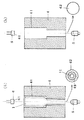
この発明の採液チップ検出方法の第1の実施例を図面とともに説明する。図1は、採液チップの定位置、発光素子及び受光素子の位置関係を示す軸方向断面図であり、図1(a)は採液チップが定位置に有るときの状態、図1(b)は採液チップが定位置に無いときの状態をあらわす。
【0014】
図中、採液チップ1は、着色された半透明樹脂材料からなり、吸引ノズルに装着される側の外径3〜5mm程度の大径部と検液を採取する側の外径1mm前後の小径部とが連なった径違い管形状をなしている。採液チップ1を吸引ノズル2に装着した後、検液を採取する方法は、図4とともに説明した従来技術と同様である。
【0015】
採液チップ1は、吸引ノズルに装着される前は、不透明樹脂材料からなるラック4の貫通孔41に小径部を下にして鉛直方向に収納されている。貫通孔41は、採液チップ1の外周形状とほぼ相補する形状をなす。従って、採液チップ1が貫通孔41に収納されているとき、採液チップ1の軸線は貫通孔41のそれと一致する。そして、採液チップ1は、貫通孔41内を、吸引ノズル2に装着される前の定位置とする。
【0016】
貫通孔41の下側開口面42に接近して発光素子としての発光ダイオード5、同じく上側開口面に接近して受光素子としてのフォトトランジスタ6が、その中心線を貫通孔41の軸線に合わせて設置されている。
【0017】
発光ダイオード5の発光面積は、貫通孔の下側開口面42のそれと同等か又はより広く、且つ両者は充分接近している。従って、下側開口面42の面積を拡散光源面と近似することができ、この実施例では、採液チップ1が貫通孔41に収納されているか否かを、以下のように判別する。
【0018】
採液チップ1が貫通孔41に収納されていない状態(図1(b))における受光素子6への入光エネルギーFs1は、
Fs1≒F1×ω1/2π
ただし、F1:発光ダイオード5から発する光エネルギー
ω1:貫通孔41の下側開口面42から見たフォトトランジスタ6の受光面61の立体角
で示される。
【0019】
一方、採液チップ1が収納されている状態(図1(a))における受光素子への入光エネルギーFs2は、
Fs2≒F1×(ω2/2π+η×ω3/2π)
ただし、ω2:採液チップ1の下側開口面11から見たフォトトランジスタ6の受光面61の立体角
ω3:貫通孔41の下側開口面42と採液チップ1の下側開口面11との間隙43から見たフォトトランジスタ6の受光面61の立体角
η :発光ダイオード5側からみた採液チップ1材料にあてられる光の平均透過率
で示される。
【0020】
平均透過率ηが充分小さいとき、近似的にFs2は、
Fs2≒F1×ω2/2π
となるから、採液チップ1が貫通孔41内に有るときと無いときの入光エネルギー比は、
Fs2/Fs1≒ω2/ω1
のように立体角の比で示される。よって、そのエネルギー差を電気信号等の出力に変換することで、採液チップの有無を検出することができる。
【0021】
この実施例において、検出機構として別途に設ける必要があるのは、発光ダイオード5及びフォトトランジスタ6であるが、それら素子を貫通孔41の軸線上に設置しているので、平面的にはそれら素子の設置に伴って占有面積が拡大することはない。
【0022】
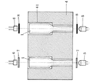
−実施例2−
バイオハザードのために採液チップは使い捨てにされる。従って、複数の測定項目又は複数の検液を連続して分析できるように、1つのラックに貫通孔が多数設けられ、複数本の採液チップが収納されることがある。そんなとき、複数本の採液チップの有無を同時検出するために、実施例1の検出機構を複数並置するだけでは、隣の発光素子から洩れる光によって受光素子が誤動作する可能性がある。
【0023】
この発明の第2の実施例は、複数の採液チップの定位置を接近させても誤検出しない構成例を示すものである。この実施例の検出機構は、図2に示される。図中、検出機構の基本構造は図1と同一である。
【0024】
ただし、1つのラック4に貫通孔41が複数設けられ、それに対応して発光ダイオード5及びフォトトランジスタ6が複数組設けられている点で、図1と異なる。そして、それぞれの発光ダイオード5と貫通孔41との間及びフォトトランジスタ6と貫通孔41との間に、所定範囲の波長の光のみ透過させるフィルタ7、7、8、8が配置されている。上下のフィルタ7、7の透過帯域は同じであるが、隣り合うフィルタ7、8は互いに透過帯域が異なるように、フィルタの種類が選択されている。例えば図面左側のフィルタ7、7として透過帯域610nmのものを配置し、右側のフィルタ8、8として透過帯域820nmのものを配置すると言った具合である。
【0025】
検出方法は、実施例1と同様に入光エネルギー差に基づくが、この例によれば、左右のフィルタの透過帯域が異なるので、隣の発光ダイオードから発せられる光がフォトトランジスタに入射することはない。従って、隣り合う発光ダイオードから発せられる光の相互干渉を防ぐことができ、複数の採液チップの定位置が接近していても正確に検出することができる。その結果、分析装置を小型化することができる。
【0026】
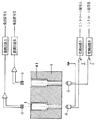
−実施例3−
この例も実施例2と同じく、1つのラックに複数本の採液チップが収納されているときに、それらの有無を同時検出する方法である。この例では、図2のフィルタに代えて、各発光ダイオード5及び各フォトトランジスタ6にそれぞれ変調回路及び復調回路が接続されている。そして、隣り合う発光ダイオード5から発せられる光は、互いに異なる変調方式又は変調度で変調され、フォトトランジスタ6で受光した後、それぞれの変調に対応して復調され、検出信号として取り出される。例えば、図面左側の発光ダイオード5から発せられる光は1kHz、右側の発光ダイオード5から発せられる光は5kHzに周波数変調がなされている。このようにしても実施例2と同様に光の相互干渉を防ぐことができる。
【0027】
【発明の効果】
以上のように、この発明の採液チップ検出方法によれば、検出機構のために特別に占有面積を拡大する必要がないので、卓上型分析装置における採液チップ欠落防止のために有用である。
【図面の簡単な説明】
【図1】実施例1の採液チップ検出方法に用いられる検出機構を示す断面図である。
【図2】実施例1の採液チップ検出方法に用いられる検出機構を示す断面図である。
【図3】実施例1の採液チップ検出方法に用いられる検出機構を示す回路図である。
【図4】採液チップによって検液が採取されるところを示す説明図である。
【図5】従来の採液チップ検出方法に用いられる検出機構を説明する図である。
【符号の説明】
1 採液チップ
2 吸引ノズル
3 容器
4 ラック
41 貫通孔
5 発光ダイオード(発光素子)
6 フォトトランジスタ(受光素子)
7,8 フィルタ[0001]
BACKGROUND OF THE INVENTION
The present invention belongs to a method for detecting whether or not a liquid collection chip is in a fixed position. In particular, it is suitable for a chip detection method for collecting a predetermined amount of test solution necessary for analysis from a test vessel such as a blood collection tube or urine collection tube.
[0002]
[Prior art]
In order to chemically analyze a liquid such as blood or urine, it is necessary to collect the liquid quantitatively. As shown in FIG. 4, the general sampling method is to immerse the
[0003]
However, due to forgetting to set the chip in the rack, set leakage, or when using only a part of the multiple chips in the rack and measuring with the remaining chips the next day, the tip of the suction nozzle If the test solution is sucked directly with the suction nozzle without attaching a sample tip, problems such as clogging of the suction nozzle, contamination of the analyzer due to the test solution, and turbidity with different test solutions occur. Therefore, it is important to confirm that the collection tip is attached to the tip of the suction nozzle.
[0004]
As a confirmation method, as shown in FIG. 5, light is applied to the outer peripheral side surface of the chip and the reflected light is detected (FIG. 5 (a)). Is provided in the rack, and a signal associated with the swing of the mechanical contact is detected (FIG. 5B).
[0005]
[Problems to be solved by the invention]
However, in the above conventional confirmation method, in addition to the area for arranging the chip, a plane area for the detection mechanism such as the light source and the mechanical contact to occupy is required, and the plane area of the entire analyzer increases. .
[0006]
SUMMARY OF THE INVENTION Therefore, an object of the present invention is to provide a liquid collection chip detection method in which the flat area of the liquid collection chip detection mechanism can be reduced.
[0007]
[Means for Solving the Problems]
In order to achieve the object, the liquid collection chip detection method of the present invention comprises:
In the method of detecting whether or not the tubular liquid collecting chip attached to the suction nozzle is in a fixed position before mounting, the light emitting element and the light receiving element are arranged on the axis of the liquid collecting chip when it is assumed to be in the fixed position. It is arranged to face each other, and is detected by the amount of light energy emitted from the light emitting element and entering the light receiving element.
[0008]
In the present invention, it is necessary to separately provide a light-emitting element and a light-receiving element as a detection mechanism, but since these elements are installed on the axis of the liquid collection chip, the elements are installed in a plan view. Accordingly, the occupied area does not increase. When the liquid collection chip is not in the fixed position, the light emitted from the light emitting element enters the light receiving element, but when the liquid collection chip is in the fixed position, a part of the light is absorbed by the liquid collection chip. Therefore, the amount of light energy entering the light receiving element differs depending on whether or not the liquid collection chip is in a fixed position, and the presence or absence of the liquid collection chip is detected by converting the energy difference into an output such as an electric signal. be able to.
[0009]
DETAILED DESCRIPTION OF THE INVENTION
In the present invention, the light emitting element is, for example, a light emitting diode, and the light receiving element is, for example, a phototransistor.
[0010]
In the first embodiment of the present invention, the through hole of the rack made of a material that blocks the light and is provided with a through hole having a shape substantially complementary to the outer peripheral shape of the liquid collection chip is collected before being attached to the suction nozzle. This is a fixed position of the liquid chip. In this way, since the light energy emitted from the light emitting element, the inner diameter of the through hole and the inner diameter of the liquid collection chip are constant, it is possible to calculate the light incident energy ratio when there is no liquid collection chip and when there is no liquid collection chip, The design of the electric circuit becomes easy.
[0011]
Furthermore, in order to continuously collect and analyze a plurality of items or a plurality of test solutions with a plurality of liquid collection chips, a plurality of through holes are usually provided in one rack, and a plurality of liquid collection chips are stored. In such a case, a plurality of sets of light emitting elements and light receiving elements are provided corresponding to each through hole, and only light having a wavelength in a predetermined range is transmitted between each light emitting element and the through hole and between the light receiving element and the through hole. If a filter is disposed and adjacent filters have different light transmission bands, mutual interference of light emitted from adjacent light emitting elements can be prevented and detection can be performed accurately.
[0012]
Further, in place of the means for arranging the filter as described above, light emitted from adjacent light emitting elements is modulated with different modulation schemes or modulation degrees, and a demodulation circuit corresponding to each modulation is connected to the light receiving element. However, mutual interference of light can be similarly prevented.
[0013]
【Example】
Example 1
A first embodiment of the liquid collection chip detection method of the present invention will be described with reference to the drawings. FIG. 1 is a sectional view in the axial direction showing a fixed position of a liquid collection chip and a positional relationship between a light emitting element and a light receiving element. FIG. 1A is a state when the liquid collection chip is in a fixed position, and FIG. ) Shows the condition when the collection tip is not in place.
[0014]
In the figure, the
[0015]
Prior to being mounted on the suction nozzle, the
[0016]
The
[0017]
The light emitting area of the
[0018]
The incident light energy Fs1 to the
Fs1≈F1 × ω1 / 2π
Here, F1: light energy ω1 emitted from the
[0019]
On the other hand, the incident light energy Fs2 to the light receiving element in the state where the
Fs2≈F1 × (ω2 / 2π + η × ω3 / 2π)
However, ω2: solid angle ω3 of the
[0020]
When the average transmittance η is sufficiently small, Fs2 is approximately
Fs2≈F1 × ω2 / 2π
Therefore, the incident light energy ratio when the
Fs2 / Fs1≈ω2 / ω1
It is indicated by the ratio of solid angles. Therefore, the presence / absence of the liquid collection chip can be detected by converting the energy difference into an output such as an electric signal.
[0021]
In this embodiment, the light-emitting
[0022]
-Example 2-
The collection tip is made disposable for biohazard. Therefore, a plurality of through holes may be provided in one rack so that a plurality of liquid collection chips can be accommodated so that a plurality of measurement items or a plurality of test solutions can be continuously analyzed. In such a case, in order to simultaneously detect the presence / absence of a plurality of liquid collection chips, if only a plurality of detection mechanisms of Example 1 are juxtaposed, the light receiving element may malfunction due to light leaking from the adjacent light emitting element.
[0023]
The second embodiment of the present invention shows a configuration example in which erroneous detection is not performed even when the fixed positions of a plurality of liquid collection chips are brought close to each other. The detection mechanism of this embodiment is shown in FIG. In the figure, the basic structure of the detection mechanism is the same as in FIG.
[0024]
However, it differs from FIG. 1 in that a plurality of through
[0025]
The detection method is based on the difference in incident energy as in the first embodiment. However, according to this example, since the transmission bands of the left and right filters are different, the light emitted from the adjacent light emitting diode does not enter the phototransistor. Absent. Therefore, mutual interference of light emitted from adjacent light emitting diodes can be prevented, and accurate detection can be performed even when the fixed positions of a plurality of liquid collection chips are close to each other. As a result, the analyzer can be miniaturized.
[0026]
-Example 3-
Similar to the second embodiment, this example is a method for simultaneously detecting the presence or absence of a plurality of liquid collection chips in one rack. In this example, a modulation circuit and a demodulation circuit are connected to each
[0027]
【The invention's effect】
As described above, according to the liquid collection chip detection method of the present invention, it is not necessary to enlarge the occupied area specially for the detection mechanism, which is useful for preventing the liquid collection chip from being lost in the desktop analyzer. .
[Brief description of the drawings]
FIG. 1 is a cross-sectional view showing a detection mechanism used in a liquid collection chip detection method of Example 1. FIG.
FIG. 2 is a cross-sectional view showing a detection mechanism used in the liquid collection chip detection method of Example 1.
FIG. 3 is a circuit diagram showing a detection mechanism used in the liquid collection chip detection method of Example 1.
FIG. 4 is an explanatory view showing a state where a test liquid is collected by a liquid collecting chip.
FIG. 5 is a diagram for explaining a detection mechanism used in a conventional liquid collection chip detection method.
[Explanation of symbols]
DESCRIPTION OF
6 Phototransistor (light receiving element)
7,8 Filter
Claims (4)
Priority Applications (1)
| Application Number | Priority Date | Filing Date | Title |
|---|---|---|---|
| JP30648095A JP3677570B2 (en) | 1995-10-30 | 1995-10-30 | Extraction chip detection method |
Applications Claiming Priority (1)
| Application Number | Priority Date | Filing Date | Title |
|---|---|---|---|
| JP30648095A JP3677570B2 (en) | 1995-10-30 | 1995-10-30 | Extraction chip detection method |
Publications (2)
| Publication Number | Publication Date |
|---|---|
| JPH09127135A JPH09127135A (en) | 1997-05-16 |
| JP3677570B2 true JP3677570B2 (en) | 2005-08-03 |
Family
ID=17957532
Family Applications (1)
| Application Number | Title | Priority Date | Filing Date |
|---|---|---|---|
| JP30648095A Expired - Fee Related JP3677570B2 (en) | 1995-10-30 | 1995-10-30 | Extraction chip detection method |
Country Status (1)
| Country | Link |
|---|---|
| JP (1) | JP3677570B2 (en) |
Family Cites Families (6)
| Publication number | Priority date | Publication date | Assignee | Title |
|---|---|---|---|---|
| JPS59147268A (en) * | 1983-01-21 | 1984-08-23 | ザ パーキン―エルマー コーポレイション | Method and device for automatically moving liquid sample among plurality of vessel |
| JPS62115348A (en) * | 1985-09-30 | 1987-05-27 | モレキユラ− デバイスイズ コ−ポレイシヨン | Device and method of measuring luminous intensity by multiple beam |
| JPH0619321B2 (en) * | 1986-06-27 | 1994-03-16 | 東ソー株式会社 | Absorbance measuring device for microplate |
| DE4023182A1 (en) * | 1990-07-20 | 1992-01-23 | Kodak Ag | Device for moving pipettes in analyser - moves plate shaped pipette tray to processing station of analyser for alignment with pipette tray resting on moving unit |
| JPH0579472U (en) * | 1992-03-27 | 1993-10-29 | 株式会社島津製作所 | Dispenser tip mounting state detector |
| JPH07270426A (en) * | 1994-03-31 | 1995-10-20 | Suzuki Motor Corp | Agglutination data collecting apparatus for blood etc. |
-
1995
- 1995-10-30 JP JP30648095A patent/JP3677570B2/en not_active Expired - Fee Related
Also Published As
| Publication number | Publication date |
|---|---|
| JPH09127135A (en) | 1997-05-16 |
Similar Documents
| Publication | Publication Date | Title |
|---|---|---|
| AU641130B2 (en) | Coded cuvette for use in testing apparatus | |
| EP1484601B1 (en) | Optical arrangement for assay reading device | |
| US4859864A (en) | Sensor and method for detecting the presence of air bubbles in liquid | |
| CN100374863C (en) | Automated point of care detection system including complete sample processing capabilities | |
| JP3255597B2 (en) | Methods and devices for determining the presence of hemolysis, jaundice or lipemia, methods for determining serum index, methods and devices for transferring samples, and methods and devices for performing pre-tests | |
| US20060008896A1 (en) | Electronic analyte assaying device | |
| US20110033341A1 (en) | Test element analysis system | |
| US20050036148A1 (en) | Optical arrangement for assay reading device | |
| CN108351292A (en) | Porous speculum for carrying out optical detection to the analyte in fluid | |
| CN101285762B (en) | Multi-parameter immunity-chromatography test strip quantitative determination instrument | |
| JPH02284064A (en) | Automatic analyzer | |
| CN101806726A (en) | Double-wavelength absorbance detection device for analyzing trace liquid | |
| EP3458839A1 (en) | Evanescent hemolysis detection | |
| CN102128830B (en) | Immunochromatographic test paper strip color signal quantitative detector | |
| JP3677570B2 (en) | Extraction chip detection method | |
| JP2004245830A (en) | Molded small-quantity waveguided optical format | |
| TW201604533A (en) | Portable electronic assay device, portable assay device and kit thereof | |
| CN201382904Y (en) | Bottle-packed liquid foreign body detection device | |
| CN208076398U (en) | A kind of portable dry type fluorescence detector | |
| CN217586807U (en) | Hematocrit value detection device and specific protein analyzer | |
| CN107152953B (en) | Liquid level detection method and device suitable for sample adding of glycosylated hemoglobin | |
| CN216979104U (en) | Blood coagulation analyzer | |
| JP2004061222A (en) | Micro biochemical evaluation apparatus | |
| CN216051348U (en) | Detection apparatus for detect liquid refracting index based on light stream accuse chip | |
| CN201382905Y (en) | Modulating signal foreign matter analysis detecting device |
Legal Events
| Date | Code | Title | Description |
|---|---|---|---|
| A977 | Report on retrieval |
Free format text: JAPANESE INTERMEDIATE CODE: A971007 Effective date: 20040517 |
|
| A131 | Notification of reasons for refusal |
Free format text: JAPANESE INTERMEDIATE CODE: A131 Effective date: 20040609 |
|
| TRDD | Decision of grant or rejection written | ||
| A01 | Written decision to grant a patent or to grant a registration (utility model) |
Free format text: JAPANESE INTERMEDIATE CODE: A01 Effective date: 20050401 |
|
| A61 | First payment of annual fees (during grant procedure) |
Free format text: JAPANESE INTERMEDIATE CODE: A61 Effective date: 20050419 |
|
| R150 | Certificate of patent or registration of utility model |
Free format text: JAPANESE INTERMEDIATE CODE: R150 |
|
| FPAY | Renewal fee payment (event date is renewal date of database) |
Free format text: PAYMENT UNTIL: 20090520 Year of fee payment: 4 |
|
| FPAY | Renewal fee payment (event date is renewal date of database) |
Free format text: PAYMENT UNTIL: 20090520 Year of fee payment: 4 |
|
| FPAY | Renewal fee payment (event date is renewal date of database) |
Free format text: PAYMENT UNTIL: 20100520 Year of fee payment: 5 |
|
| FPAY | Renewal fee payment (event date is renewal date of database) |
Free format text: PAYMENT UNTIL: 20100520 Year of fee payment: 5 |
|
| FPAY | Renewal fee payment (event date is renewal date of database) |
Free format text: PAYMENT UNTIL: 20110520 Year of fee payment: 6 |
|
| FPAY | Renewal fee payment (event date is renewal date of database) |
Free format text: PAYMENT UNTIL: 20120520 Year of fee payment: 7 |
|
| FPAY | Renewal fee payment (event date is renewal date of database) |
Free format text: PAYMENT UNTIL: 20130520 Year of fee payment: 8 |
|
| R250 | Receipt of annual fees |
Free format text: JAPANESE INTERMEDIATE CODE: R250 |
|
| R250 | Receipt of annual fees |
Free format text: JAPANESE INTERMEDIATE CODE: R250 |
|
| LAPS | Cancellation because of no payment of annual fees |