JP3672384B2 - Sense circuit - Google Patents
Sense circuit Download PDFInfo
- Publication number
- JP3672384B2 JP3672384B2 JP19500496A JP19500496A JP3672384B2 JP 3672384 B2 JP3672384 B2 JP 3672384B2 JP 19500496 A JP19500496 A JP 19500496A JP 19500496 A JP19500496 A JP 19500496A JP 3672384 B2 JP3672384 B2 JP 3672384B2
- Authority
- JP
- Japan
- Prior art keywords
- activation signal
- mos transistor
- gate
- sense amplifier
- drain
- Prior art date
- Legal status (The legal status is an assumption and is not a legal conclusion. Google has not performed a legal analysis and makes no representation as to the accuracy of the status listed.)
- Expired - Fee Related
Links
- 230000004913 activation Effects 0.000 claims description 145
- 230000007274 generation of a signal involved in cell-cell signaling Effects 0.000 claims description 23
- 230000000295 complement effect Effects 0.000 claims description 11
- 230000003213 activating effect Effects 0.000 claims description 8
- 239000003990 capacitor Substances 0.000 claims description 8
- 108010075750 P-Type Calcium Channels Proteins 0.000 claims 11
- 108090000699 N-Type Calcium Channels Proteins 0.000 claims 7
- 102000004129 N-Type Calcium Channels Human genes 0.000 claims 7
- 108091006146 Channels Proteins 0.000 claims 4
- 238000010586 diagram Methods 0.000 description 27
- 230000000694 effects Effects 0.000 description 9
- 230000002093 peripheral effect Effects 0.000 description 3
- 230000007423 decrease Effects 0.000 description 2
- 238000007599 discharging Methods 0.000 description 2
- 230000003071 parasitic effect Effects 0.000 description 2
- 230000000717 retained effect Effects 0.000 description 2
- 230000006866 deterioration Effects 0.000 description 1
- 239000004065 semiconductor Substances 0.000 description 1
- 230000009466 transformation Effects 0.000 description 1
Images


Classifications
-
- G—PHYSICS
- G11—INFORMATION STORAGE
- G11C—STATIC STORES
- G11C11/00—Digital stores characterised by the use of particular electric or magnetic storage elements; Storage elements therefor
- G11C11/21—Digital stores characterised by the use of particular electric or magnetic storage elements; Storage elements therefor using electric elements
- G11C11/34—Digital stores characterised by the use of particular electric or magnetic storage elements; Storage elements therefor using electric elements using semiconductor devices
- G11C11/40—Digital stores characterised by the use of particular electric or magnetic storage elements; Storage elements therefor using electric elements using semiconductor devices using transistors
- G11C11/401—Digital stores characterised by the use of particular electric or magnetic storage elements; Storage elements therefor using electric elements using semiconductor devices using transistors forming cells needing refreshing or charge regeneration, i.e. dynamic cells
- G11C11/4063—Auxiliary circuits, e.g. for addressing, decoding, driving, writing, sensing or timing
- G11C11/407—Auxiliary circuits, e.g. for addressing, decoding, driving, writing, sensing or timing for memory cells of the field-effect type
- G11C11/409—Read-write [R-W] circuits
- G11C11/4091—Sense or sense/refresh amplifiers, or associated sense circuitry, e.g. for coupled bit-line precharging, equalising or isolating
-
- G—PHYSICS
- G11—INFORMATION STORAGE
- G11C—STATIC STORES
- G11C11/00—Digital stores characterised by the use of particular electric or magnetic storage elements; Storage elements therefor
- G11C11/21—Digital stores characterised by the use of particular electric or magnetic storage elements; Storage elements therefor using electric elements
- G11C11/34—Digital stores characterised by the use of particular electric or magnetic storage elements; Storage elements therefor using electric elements using semiconductor devices
- G11C11/40—Digital stores characterised by the use of particular electric or magnetic storage elements; Storage elements therefor using electric elements using semiconductor devices using transistors
- G11C11/401—Digital stores characterised by the use of particular electric or magnetic storage elements; Storage elements therefor using electric elements using semiconductor devices using transistors forming cells needing refreshing or charge regeneration, i.e. dynamic cells
- G11C11/4063—Auxiliary circuits, e.g. for addressing, decoding, driving, writing, sensing or timing
- G11C11/407—Auxiliary circuits, e.g. for addressing, decoding, driving, writing, sensing or timing for memory cells of the field-effect type
- G11C11/4074—Power supply or voltage generation circuits, e.g. bias voltage generators, substrate voltage generators, back-up power, power control circuits
-
- G—PHYSICS
- G11—INFORMATION STORAGE
- G11C—STATIC STORES
- G11C11/00—Digital stores characterised by the use of particular electric or magnetic storage elements; Storage elements therefor
- G11C11/21—Digital stores characterised by the use of particular electric or magnetic storage elements; Storage elements therefor using electric elements
- G11C11/34—Digital stores characterised by the use of particular electric or magnetic storage elements; Storage elements therefor using electric elements using semiconductor devices
- G11C11/40—Digital stores characterised by the use of particular electric or magnetic storage elements; Storage elements therefor using electric elements using semiconductor devices using transistors
- G11C11/401—Digital stores characterised by the use of particular electric or magnetic storage elements; Storage elements therefor using electric elements using semiconductor devices using transistors forming cells needing refreshing or charge regeneration, i.e. dynamic cells
- G11C11/4063—Auxiliary circuits, e.g. for addressing, decoding, driving, writing, sensing or timing
- G11C11/407—Auxiliary circuits, e.g. for addressing, decoding, driving, writing, sensing or timing for memory cells of the field-effect type
- G11C11/409—Read-write [R-W] circuits
- G11C11/4094—Bit-line management or control circuits
-
- G—PHYSICS
- G11—INFORMATION STORAGE
- G11C—STATIC STORES
- G11C5/00—Details of stores covered by group G11C11/00
- G11C5/14—Power supply arrangements, e.g. power down, chip selection or deselection, layout of wirings or power grids, or multiple supply levels
- G11C5/147—Voltage reference generators, voltage or current regulators; Internally lowered supply levels; Compensation for voltage drops
-
- G—PHYSICS
- G11—INFORMATION STORAGE
- G11C—STATIC STORES
- G11C7/00—Arrangements for writing information into, or reading information out from, a digital store
- G11C7/06—Sense amplifiers; Associated circuits, e.g. timing or triggering circuits
- G11C7/065—Differential amplifiers of latching type
-
- G—PHYSICS
- G11—INFORMATION STORAGE
- G11C—STATIC STORES
- G11C7/00—Arrangements for writing information into, or reading information out from, a digital store
- G11C7/12—Bit line control circuits, e.g. drivers, boosters, pull-up circuits, pull-down circuits, precharging circuits, equalising circuits, for bit lines
Description
【0001】
【発明の属する技術分野】
本発明は、半導体メモリに接続されたビット線の間の電位差を検知してそれを増幅するセンス回路に関するものである。
【0002】
【従来の技術】
図2は、従来のDRAMの要部を示す回路図である。
DRAMでは、メモリセルアレイ1中に複数のメモリセルM1,M2,…を備えている。各メモリセルM1,M2,…は同様の構成であり、平行平板容量2とNチャネル型MOSトランジスタ(以下、NMOSという)3とを有している。各容量2の一方の電極は、NMOS3のソースに接続され、該容量2の他方の電極には、セルプレート電位を設定する基準電位VCPが与えられる接続になっている。図2中のメモリセルM1におけるNMOS3のドレインは、ビット線BLに接続され、該NMOS3のゲートがワード線WL0に接続されている。メモリセルM2のNMOS3のドレインは、ビット線BLBに接続され、この該NMOS3のゲートが、ワード線WL1に接続されている。
メモリセルアレイ1から導出されたビット線対BL,BLBには、イコライズ回路4が接続されている。イコライズ回路4は各ビット線BL,BLBの電位を同一レベルに設定するものであり、ビット線プリチャージ用の基準電位VBLがソースに接続された2個のNMOS4a,4bを備えている。各NMOS4a,4bのドレインは、ビット線対BL,BLBにそれぞれ接続され、これらNMOS4a,4bのゲートには、制御信号EQM が共通に与えられるようになっている。各基準電位VCP及び基準電位VBLは、共に電源電位VCCの約1/2の中間電位であり、VCP発生回路5及びVBL発生回路6でそれぞれ生成されて与えられる構成である。
【0003】
ビット線対BL,BLBの先に、センス回路10が接続されている。
センス回路10において、ビット線対BL,BLBはトランスファゲートを構成する2つのNMOS11,12を介してセンスアンプノードNA,NABにそれぞれ接続されている。即ち、各NMOS11,12のゲートには、制御信号TGが入力され、該制御信号TGに基づきNMOS11,12がオンして各ノードNA,NABとビット対BL,BLBとが、それぞれ接続される構成である。
ノードNAとノードNABの間には、ソース同士が接続された2つのPチャネル型MOSトランジスタ(以下、PMOSという)13a,13bで構成されたセンスアンプ13と、ソース同士が接続された2つのNMOS14a,14bで構成されたセンスアンプ14とが、設けられている。ノードNAは、PMOS13a及びNMOS14aのドレインと、PMOS13b及びNMOS14bのゲートに接続されている。ノードNABは、PMOS13b及びNMOS14bのドレインと、PMOS13a及びNMOS14aのゲートに接続されている。
【0004】
PMOS13a,13bのソースは、ソースが電源電位VCCに接続されたPMOS15のドレインに接続されている。NMOS14a,14bのソースは、ソースが電源電位VSSに接続されたNMOS16のドレインに接続されている。NMOS16のゲートには、センス開始信号SLNGB がインバータ17を介して信号SLNGとなって与えられる構成になっている。NMOS15には、信号SLNGがインバータ18を介して信号SLPGになって与えられる構成である。各インバータ17,18は、電源電位VCCと電源電位VSS間に接続され、入力信号のレベルに応じて出力信号のレベルを電位VCCまたは電位VSSに設定する構成である。
実際のDRAMでは、メモリセルアレイ1からは複数組のビット線対BL,BLBが導出されているので、それらに対応して複数のセンス回路10がアレイ化されている。ただし、PMOS15、NMOS16、及びインバータ17,18は、複数のセンス回路10で共用される構成である。
図3は、図2の動作を示す波形図であり、この図3を参照しつつ、DRAMの動作を説明する。
【0005】
制御信号EQM が“H”レベルから“L”レベルに変化することで、イコライズ回路4中のNMOS4a,4bがオフ状態になり、ビット線対BL,BLBが基準電位VBLから切り離される。この状態で、ワード線WL0が選択されて昇圧レベルの電位VCC+Vt +αに立ち上がると、ビット線対BL,BLBの間に、メモリセルの情報に応じた微小電位差が生じる。ワード線WL0の立ち上がるのと同時に、制御信号TGも昇圧レベルの電位VCC+Vt +αに立ち上がり、NMOS11,12がオンする。これにより、ビット線対BL,BLBがノードNA,NABに接続される。
【0006】
センス動作は、センス開始信号SLNGB が“H”レベルから“L”レベルに変化することで開始される。センス開始信号SLNGB が“L”レベルに変化すると、インバータ17により、センスアンプ活性化信号SLNGが“L”レベルから“H”レベル(電位VCC) に変化し、センスアンプ活性化信号SLPGが“H”レベルから “L”レベル(電位VSS)に変化する。これにより、PMOS15とNMOS16が共にオン状態になって、センスアンプ13,14が活性化する。活性化したセンスアンプ13,14によって、ビット線対BL,BLBとノードNA,NABにおける微小電位差が感知され、ビット線対BL,BLBに対するPMOS15とNMOS16を介した充放電が行われて微小電位差が増幅される。
【0007】
【発明が解決しようとする課題】
しかしながら、従来のDRAMでは、次のような課題があった。
センス回路10のセンス動作で発生するビット線対BL,BLBの充放電電流と、PMOS15とNMOS16に電源電位VCC,VSSを供給する配線の寄生抵抗とによる電圧降下のため、電源電位VCC,VSSに電源ノイズが発生する。この電源ノイズのため、従来のDRAMでは、周辺回路の動作マージンが悪化していた。
【0008】
【課題を解決するための手段】
センス回路は、ビット線対に接続され、メモリセルの保持データに応じた該ビット線対の間の微小電位差を感知する第1及び第2のセンスアンプと、そのビット線対と第1及び第2のセンスアンプの間の導通制御を行うトランスファゲートとを有している。さらに、センス回路は、与えられた制御信号に基づき、論理レベルが互いに相補的な第1の活性化信号と第2の活性化信号とを生成する活性化信号生成回路と、第1のセンスアンプと第1の電源電位との間に接続され、ゲートに入力された第1の活性化信号に基づきオン、オフし、このオン状態のとき該第1のセンスアンプを活性化する第1のMOSトランジスタと、第2のセンスアンプと第1の電源電位よりも高い第2の電源電位との間に接続され、第2の活性化信号をゲートに入力してオン、オフし、このオン状態のとき該第2のセンスアンプを活性化する第2のMOSトランジスタとを、備えている。そして、第1及び第2のセンスアンプを活性化して各ビット線に対する第1及び第2の電源電位からの充放電を行い、ビット線対の間の微小電位差を保持データの論理レベルに対応した電位差に設定する構成である。
【0009】
前記課題を解決するために、第1〜第5の発明は、センス回路中の活性化信号生成回路を次のような構成にしている。即ち、第1〜第5の発明における活性化信号生成回路は、第2の活性化信号の論理レベルのうちの第2のMOSトランジスタをオン状態にする論理レベルを、第1の電源電位と第2の電源電位の間の中間電位に設定する構成にしている。
第1〜第5の発明によれば、以上のようにセンス回路を構成したので、第1の活性化信号と第2の活性化信号が第1及び第2のMOSトランジスタのゲートに与えられて、第1及び第2のセンスアンプが活性化する。これにより、ビット線対の間の微小電位差が、保持データの論理レベルに対応した電位差に設定される。ここで、第2の活性化信号のレベルは、第1の電源電位と第2の電源電位の間の中間電位に設定されているので、第2のMOSトランジスタの動作領域が従来とは異なると共に、該第2のMOSトランジスタにおけるオン抵抗が増加する。従って、前記課題を解決することができる。
【0010】
【発明の実施の形態】
第1の実施形態
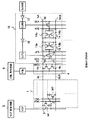
図1は、本発明の第1の実施形態を示すDRAMの要部の回路図である。
このDRAMでは、メモリセルアレイ20中に複数のメモリセルM1,M2,…を備えている。各メモリセルM1,M2,…は同様の構成であり、容量素子である平行平板容量21とNMOS22とで構成されている。各容量21の一方の電極は、NMOS22のソースに接続され、該容量21の他方の電極には、セルプレート電位を設定する第1の基準電位である電位VCPが与えられる接続になっている。電位VCPは、第1の電源電位VSSと第2の電源電位VCCの中間の、約1/2VCCの電位であり、VCP発生回路23で生成されたものである。
図1中のメモリセルM1におけるNMOS22のドレインは、ビット線BLに接続され、該NMOS22のゲートがワード線WL0に接続されている。メモリセルM2のNMOS22のドレインは、ビット線BLBに接続され、この該NMOS22のゲートが、ワード線WL1に接続されている。メモリセルアレイ20から導出されたビット線対BL,BLBには、イコライズ回路25が接続されている。
【0011】
イコライズ回路25は各ビット線BL,BLBの電位を同一レベルに設定するものであり、ビット線プリチャージ用の第2の基準電位VBLがソースに与えられた2個のNMOS25a,25bを備えている。各NMOS25a,25bのドレインは、ビット線対BL,BLBにそれぞれ接続され、これらNMOS25a,25bのゲートには、プリチャージ制御信号EQM が共通に与えられるようになっている。電位VBLは、第1の電源電位VSSと第2の電源電位VCCの中間の約1/2VCCの電位であり、VBL発生回路26で生成されたものである。ビット線対BL,BLBの先に、センス回路30が接続されている。
センス回路30において、ビット線対BL,BLBは、トランスファゲートを構成する2つのNMOS31,32を介してセンスアンプノードNA,NABにそれぞれ接続されている。即ち、各NMOS31,32のゲートには、制御信号TGが入力され、該制御信号TGに基づきNMOS31,32がオンし、ノードNA,NABとビット対BL,BLBとが接続される構成である。
【0012】
ノードNAとノードNABの間には、第1及び第2のセンスアンプ33,34が接続されている。センスアンプ33は、ソース同士が接続された2つのNMOS33a,33bで構成されている。センスアンプ34は、ソース同士が接続された2つのPMOS34a,34bで構成されている。ノードNAは、NMOS33a及びPMOS34aのドレインと、NMOS33b及びPMOS34bのゲートに接続されている。ノードNABは、NMOS33b及びPMOS34bのドレインと、NMOS33a及びPMOS34aのゲートに接続されている。NMOS33a,34bのソースは、ソースが電源電位VSSに接続された第1のMOSトランジスタであるNMOS35のドレインに接続されている。PMOS34a,34bのソースは、ソースが電源電位VCCに接続された第2のMOSトランジスタであるPMOS36のドレインに接続されている。
【0013】
このセンス回路30には、さらに、第1の活性化信号SLNGと第2の活性化信号SLPGとを生成する活性化信号生成回路が設けられている。活性化信号生成回路は、第1手段のインバータ37と第2手段のインバータ38とで構成されている。インバータ37には、制御信号であるセンス開始信号SLNGB がゲート入力され、該該インバータ37が活性化信号SLNGを出力する構成である。インバータ38は、活性化信号SLNGに対して相補的論理レベルを示す活性化信号SLPGを出力するものであり、PMOS38aとNMOS38bで構成されている。これらPMOS38aとNMOS38bのゲートには活性化信号SLNGが共通に入力されると共に、そのドレイン同士は接続されている。PMOS38aのソースは電源電位VCCに接続されている。NMOS38bのソースは、従来とは異なり、基準電位VBLに接続されている。インバータ37の出力する活性化信号SLNGがNMOS35のゲートに与えられ、インバータ38の出力する活性化信号SLPGがPMOS36のゲートに与えられる接続である。
【0014】
図1では簡単のためセンス回路30を一つのみ示しているが、通常のDRAMでは、メモリセルアレイ20からは複数組のビット線対BL,BLBが導出されているので、それらに対応して複数のセンス回路30がアレイ化されている。ただし、NMOS35、PMOS36、及びインバータ37,38は、複数のセン 回路30で共用される構成である。
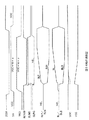
図4は、図1の動作を示す波形図であり、この図4を参照しつつ、DRAMの動作を説明する。
プリチャージ制御信号EQM が、図4のタイミングで、“H”レベルから“L”レベルに変化することで、イコライズ回路25中のNMOS25a,25bがオフ状態になり、ビット線対BL,BLBが基準電位VBLから切り離される。この状態で、ワード線WL0が選択されて昇圧レベルの電位VCC+Vt +αに立ち上がると、ビット線対BL,BLBの間に、メモリセルの保持情報に応じた微小電位差が生じる。ワード線WL0の立ち上がるのと同時に、制御信号TGも昇圧レベルの電位VCC+Vt +αに立ち上がり、トランスファゲートのNMOS31,32がオンする。これにより、ビット線対BL,BLBが、ノードNA,NABに接続される。
【0015】
センス動作は、センス開始信号SLNGB が“H”レベルから“L”レベルに変化することで開始される。センス開始信号SLNGB が“L”レベルに変化すると、インバータ37により、活性化信号SLNGが“L”レベルから“H”レベル(電位VCC) に変化し、NMOS38bがオンして活性化信号SLPGが“H”レベルから “L”レベルに変化する。活性化信号SLPGの“L”レベルは、NMOS38bによって、基準電位VBLに設定される。
これにより、活性化信号SLNGの“H”レベルを入力するNMOS35と、活性化信号SLPGの“L”レベルを入力するPMOS36が共にオン状態になり、センスアンプ33,34が活性化する。活性化したセンスアンプ33,34によって、ビット線対BL,BLBとノードNA,NABにおける微小電位差が感知され、ビット線対BL,BLBに対するPMOS36とNMOS35を介した充放電が行われる。そして、各ビット線BL,BLBの電位差が、メモリセルの保持するデータに対応した値になる。
以上のように、この第1の実施形態では、インバータ38の出力する活性化信号SLPGの“L”レベルは、基準電位VBL(1/2VCC)に設定され、該基準電位VBLがPMOS36のゲートに与えられる構成である。従って、次の(a)〜(c)のような効果が得られる。
【0016】
(a) PMOS36におけるオン抵抗は、従来のように電位VSSでオン状態になる場合よりも大きくなり、充放電を行う際の該PMOS36での電圧降下が大きくなる。そのため、電源電位V CCを供給する配線における寄生抵抗での電圧降下が最小限に抑えられ、周辺回路の動作マージンが悪化しない。
(b) PMOS36のゲート電位が、基準電位VBL(1/2VCC)に設定されるので、該PMOS36でのドレイン電流対ドレイン・ソース間電圧特性が、従来とは異なり、定電流源でビット線対BL,BLBへの充電を行っているのに近くなり、充電のピーク電流を低減できる。
(c) ビット線対BL,BLBをプリチャージする電位VBLで、PMOS36をオンさせるので、ビット線対BL,BLBのプリチャージ状態をモニタして、充電電流を選択することになり、電位VBLの値が変化しても、その値にかかわらず、常に一定のビット線対BL,BLBの充電スピードが得られる。例えば、ビット線BLのプリチャージ電位が1/2VCC+δVの場合には、ビット線BLに対する充電電流はδV分の電荷量が少なくてよい。このときには、活性化信号SLPGの電位レベルもδV上昇し、PMOS36のセンスアンプ33への活性化能力が低下する。即ち、ビット線BLに対する充電電流の減少分、PMOS36に対する活性化能力が低下し、充電スピードが変わらない。
【0017】
第2の実施形態
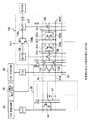
図5は、本発明の第2の実施形態を示すDRAMの要部の回路図であり、図1中の要素と共通する要素には共通の符号が付されている。
このDRAMは、第1の実施形態と同様のメモリセルアレイ20と、イコライズ回路25と、VCP発生回路23と、VBL発生回路26と、図1とは異なるセンス回路40とを備えている。
センス回路40は、ビット線対BL,BLBの先に接続されている。センス回路40において、ビット線対BL,BLBは、トランスファゲートを構成する2つのNMOS41,42を介し、センスアンプノードNA,NABにそれぞれ接続されている。ノードNAとノードNABの間には、第1及び第2のセンスアンプ43,44が接続されている。センスアンプ43は、ソース同士が接続された2つのNMOS43a,43bで構成されている。センスアンプ44は、ソース同士が接続された2つのPMOS44a,44bで構成されている。ノードNAは、NMOS43a及びPMOS44aのドレインと、NMOS43b及びPMOS44bのゲートに接続されている。ノードNABは、NMOS43b及びPMOS44bのドレインと、NMOS43a及びPMOS44aのゲートに接続されている。NMOS43a,44bのソースは、ソースが電源電位VSSに接続された第1のMOSトランジスタであるNMOS45のドレインに接続されている。PMOS44a,44bのソースは、ソースが電源電位VCCに接続された第2のMOSトランジスタであるPMOS46のドレインに接続されている。
【0018】
このセンス回路40には、さらに、第1の活性化信号SLNGと第2の活性化信号SLPGとを生成する第1の実施形態とは異なる活性化信号生成回路が設けられている。活性化信号生成回路は、第1手段のインバータ47と第2手段のインバータ48とで構成されている。インバータ47には、制御信号のセンス開始信号SLNGB がゲートに入力され、該該インバータ47が活性化信号SLNGを出力する構成である。インバータ48は、活性化信号SLNGに対して相補的論理レベルを示す活性化信号SLPGを出力するものであり、第1のPMOS48aと第2のPMOS48bとで構成されている。PMOS48aのゲートには、活性化信号SLNGが入力され、PMOS48bのゲートには、センス開始信号SLNGB が入力される接続である。PMOS48aのドレインとPMOS48bのドレインとが接続されている。PMOS48aのソースは、電源電位VCCに接続され、PMOS48bのソースは基準電位VBLに接続されている。インバータ47の出力する活性化信号SLNGが、NMOS45のゲートに与えられ、インバータ48の出力する活性化信号SLPGが、PMOS46のゲートに与えられる接続である。
【0019】
図1では簡単のためセンス回路40を一つのみ示しているが、通常のDRAMでは、メモリセルアレイ20から複数組のビット線対BL,BLBが導出されているので、それらに対応して複数のセンス回路40がアレイ化されている。ただし、NMOS45、PMOS46、及びインバータ47,48は、複数のセンス回路40で共用される構成である。
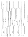
図6は、図5の動作を示す波形図であり、この図5を参照しつつ、DRAMの動作を説明する。
この第2の実施形態のDRAMの動作は、基本的に第1の実施形態と同様である。即ち、プリチャージ制御信号EQM により、イコライズ回路25中のNMOS25a,25bがオフ状態になってから、トランスファゲートのNMOS41,42がオンし、ビット線対BL,BLBがノードNA,NABに接続されるまでの動作は、第1の実施形態と同様である。センス開始信号SLNGB が“H”レベルから“L”レベルに変化することでセンス動作が開始される。センス開始信号SLNGB が“L”レベルに変化すると、インバータ47により、活性化信号SLNGが “L”レベルから“H”レベル(電位VCC) に変化する。これと同時にPMOS48bがオンして活性化信号SLPGが“H”レベルから“L”レベルに変化する。活性化信号SLPGの“L”レベルは、PMOS48bによって、基準電位VBLに設定される。
【0020】
これにより、活性化信号SLNGの“H”レベルを入力するNMOS45と、活性化信号SLPGが“L”レベルを入力するPMOS46が共にオン状態になって、センスアンプ43,44が活性化する。活性化したセンスアンプ43,44によって、ビット線対BL,BLBとノードNA,NABにおける微小電位差が感知され、ビット線対BL,BLBに対するPMOS46とNMOS45を介した充放電が行われる。そして、各ビット線BL,BLBの電位差が、メモリセルの保持するデータに対応した値になる。
以上のように、この第2の実施形態では、活性化信号SLPGの“L”レベルは、基準電位VBL(1/2VCC)に設定されてPMOS46のゲートに与えられる構成なので、第1の実施形態と同様の(a)〜(c)の効果が期待できる。そのうえ、センス開始信号SLNGB でインバータ48のPMOS48bがオンするので、活性化信号SLPGの立ち下がりをインバータ1つ分だけ速くできる。
【0021】
第3の実施形態
図7は、本発明の第3の実施形態を示すDRAMの要部の回路図であり、図1、図5中の要素と共通する要素には共通の符号が付されている。
このDRAMは、第1及び第2の実施形態と同様のメモリセルアレイ20、イコライズ回路25、VCP発生回路23及びVBL発生回路26と、図1或いは図5とは異なるセンス回路50とを、備えている。
センス回路50は、ビット線対BL,BLBの先に接続されている。センス回路50において、ビット線対BL,BLBは、トランスファゲートを構成する2つのNMOS51,52を介してセンスアンプノードNA,NABにそれぞれ接続されている。ノードNAとノードNABの間には、第1及び第2のセンスアンプ53,54が接続されている。センスアンプ53は、ソース同士が接続された2つのNMOS53a,53bで構成されている。センスアンプ54は、ソース同士が接続された2つのPMOS54a,54bで構成されている。
【0022】
ノードNAは、NMOS53a及びPMOS54aのドレインと、NMOS53b及びPMOS54bのゲートに接続されている。ノードNABは、NMOS53b及びPMOS54bのドレインと、NMOS53a及びPMOS54aのゲートに接続されている。NMOS53a,54bのソースは、ソースが電源電位VSSに接続された第1のMOSトランジスタであるNMOS55のドレインに接続されている。PMOS54a,54bのソースは、ソースが電源電位VCCに接続された第2のMOSトランジスタであるPMOS56のドレインに接続されている。
このセンス回路50には、第1の活性化信号SLNGと第2の活性化信号SLPGとを生成する第1及び第2の実施形態とは異なる活性化信号生成回路が設けられている。活性化信号生成回路は、第1手段のインバータ57と第2手段のインバータ58とで構成されている。インバータ57には、制御信号であるセンス開始信号SLNGB がゲート入力され、該インバータ57が活性化信号SLNGを出力する構成である。インバータ58は、活性化信号SLNGに対して相補的論理レベルを示す活性化信号SLPGを出力するものであり、第1のPMOS58aと第2のPMOS58bと第1のNMOS58cとで構成されている。
【0023】
PMOS58aとNMOS58cのゲートには活性化信号SLNGが共通に入力され、PMOS58bのゲートには、センス開始信号SLNGB が入力される接続になっている。PMOS58aとPMOS58bとNMOS58cのドレインは、共通に接続されている。PMOS58aのソースは、電源電位VCCに接続され、PMOS58bとNMOS58cのソースが、基準電位VBLに接続されている。インバータ57の出力する活性化信号SLNGがNMOS55のゲートに与えられ、インバータ58の出力する活性化信号SLPGが、PMOS56のゲートに与えられる接続である。
図7では簡単のためセンス回路50を一つのみ示しているが、実際のDRAMでは、それらに対応して複数のセンス回路50がアレイ化されている。
図8は、図7の動作を示す波形図であり、この図を参照しつつ、図7の動作を説明する。
【0024】
この第3の実施形態における動作も、第1及び第2の実施形態と基本的に同じである。よって、第1のブリチャージ制御信号EQM により、イコライズ回路25中のNMOS25a,25bがオフ状態になってから、トランスファゲートのNMOS51,52がオンし、ビット線対BL,BLBがノードNA,NABに接続されるまでの動作は、第1及び第2の実施形態と同様である。センス開始信号SLNGB が“H”レベルから“L”レベルに変化することでセンス動作が開始される。センス開始信号SLNGB が“L”レベルに変化すると、インバータ57により、活性化信号SLNGが“L”レベルから“H”レベル(電位VCC) に変化する。これと同時にPMOS58bがオンして活性化信号SLPGが“H”レベルから“L”レベルに変化する。PMOS58bがオンしてから、1インバータ分遅れてNMOS58cがオンする。NMOS58cがオンすることで、活性化信号SLPGのレベルが安定し、該活性化信号SLPGの“L”レベルは、基準電位VBLに設定される。
【0025】
これにより、活性化信号SLNGの“H”レベルを入力するNMOS55と、活性化信号SLPGの“L”レベルを入力するPMOS56が共にオン状態になって、センスアンプ53,54が活性化する。活性化したセンスアンプ53,54によって、ビット線対BL,BLBとノードNA,NABにおける微小電位差が感知され、ビット線対BL,BLBに対するPMOS56とNMOS55を介した充放電が行われる。そして、各ビット線BL,BLBの電位差が、メモリセルの保持するデータに対応した値になる。
以上のように、この第3の実施形態では、活性化信号SLPGの“L”レベルは、基準電位VBL(1/2VCC)に設定されてPMOS56のゲートに与えられる構成なので、第1及び第2の実施形態における(a)と(b)の効果が期待できる。そのうえ、センス開始信号SLNGB でインバータ58のPMOS58bがオンするので、活性化信号SLPGの立ち下がりをインバータ1つ分だけ速くできる。さらに、NMOS58cを設けているので、活性化信号SLPGの立ち下がり電位レベルを第2の実施形態よりも確実にできる。
【0026】
第4の実施形態
図9は、本発明の第4の実施形態を示すDRAMの要部の回路図であり、図1、図5及び図7中の要素と共通する要素には共通の符号が付されている。
前記第1の実施形態では活性化信号SLPGの電位を基準電位VBLに設定していたが、このDRAMでは、活性化信号SLPGの電位を基準電位VCPに設定することを特徴にしている。
図9のDRAMは、第1〜第3の実施形態と同様のメモリセルアレイ20、イコライズ回路25、VCP発生回路23及びVBL発生回路26を備えると共に、基準電位VCPを入力するセンス回路60を備えている。
【0027】
センス回路60の構成は、図1とほぼ同様であり、ビット線対BL,BLBが、トランスファゲートを構成する2つのNMOS61,62を介してセンスアンプノードNA,NABにそれぞれ接続されている。ノードNAとノードNABの間には、第1及び第2のセンスアンプ63,64が接続されている。センスアンプ63は、ソース同士が接続された2つのNMOS63a,63bで構成されている。センスアンプ64は、ソース同士が接続された2つのPMOS64a,64bで構成されている。ノードNAは、NMOS63a及びPMOS64aのドレインと、NMOS63b及びPMOS64bのゲートに接続されている。ノードNABは、NMOS63b及びPMOS64bのドレインと、NMOS63a及びPMOS64aのゲートに接続されている。NMOS63a,64bのソースは、ソースが電源電位VSSに接続された第1のMOSトランジスタであるNMOS65のドレインに接続されている。PMOS64a,64bのソースは、ソースが電源電位VCCに接続された第2のMOSトランジスタであるPMOS66のドレインに接続されている。
【0028】
このセンス回路60には、さらに、第1の活性化信号SLNGと第2の活性化信号SLPGとを生成する活性化信号生成回路が設けられている。活性化信号生成回路は、第1手段のインバータ67と第2手段のインバータ68とで構成されている。インバータ67には、制御信号であるセンス開始信号SLNGB がゲート入力され、該インバータ67が活性化信号SLNGを出力する構成である。インバータ68は、活性化信号SLNGに対して相補的論理レベルを示す活性化信号SLPGを出力するものであり、PMOS68aとNMOS68bとで構成されている。PMOS68aとNMOS68cのゲートには、活性化信号SLNGが共通に入力される接続になっている。PMOS68aとNMOS68bのドレインは、共通に接続されている。PMOS68aのソースは、電源電位VCCに接続され、NMOS68bのソースが基準電位VCPに接続されている。インバータ67の出力する活性化信号SLNGが、NMOS65のゲートに与えられ、インバータ68の出力する活性化信号SLPGが、PMOS66のゲートに与えられる接続である。
【0029】
図10は、図9の動作を示す波形図である。
このDRAMでは、センス回路60中のNMOS68bのソースに基準電位VBLと同じ電位(1/2VCC)の基準電位VCPが入力される構成であり、活性化信号SLPGの電位も図4と同じになる。即ち、第1の実施形態とまったく同じ動作が行われる。
以上のように、この第4の実施形態では、NMOS68bのソースに基準電位VCPを入力する構成にしているので、第1の実施形態における(c)の効果は得られないが、(a)及び(b)の効果が得られる。
【0030】
第5の実施形態
図11は、本発明の第5の実施形態を示すDRAMの要部の回路図であり、図1、図5、図7及び図9中の要素と共通する要素には共通の符号が付されている。
活性化信号SLPGの電位レベルを設定する電位は、基準電位VBLでも基準電位VCPでもどちらを用いても電源ノイズを減少させることを、第4の実施形態では説明している。この第5の実施形態では、基準電位VBLと基準電位VCPとの間がトランスファゲート等の接続手段70で接続可能な構成のDRAMを説明する。
まず、DRAMの構成を説明する。このDRAMは、第1〜第4の実施形態と同様のメモリセルアレイ20、イコライズ回路25、VCP発生回路23及びVBL発生回路26を備えている。接続手段70は、オン状態のとき基準電位VBLと基準電位VCPとを接続する構成である。
【0031】
一方、ビット線対BL,BLBの先に、センス回路80が接続されている。センス回路80の構成は、図1とほぼ同様であり、ビット線対BL,BLBが、トランスファゲートを構成する2つのNMOS81,82を介してセンスアンプノードNA,NABにそれぞれ接続されている。ノードNAとノードNABの間には、第1及び第2のセンスアンプ83,84が接続されている。センスアンプ83は、ソース同士が接続された2つのNMOS83a,83bで構成されている。センスアンプ84は、ソース同士が接続された2つのPMOS84a,84bで構成されている。
【0032】
ノードNAは、NMOS83a及びPMOS84aのドレインと、NMOS83b及びPMOS84bのゲートとに接続されている。ノードNABは、NMOS83b及びPMOS84bのドレインと、NMOS83a及びPMOS84aのゲートとに接続されている。NMOS83a,84bのソースは、ソースが電源電位VSSに接続された第1のMOSトランジスタであるNMOS85のドレインに接続されている。PMOS84a,84bのソースは、ソースが電源電位VCCに接続された第2のMOSトランジスタであるPMOS86のドレインに接続されている。
このセンス回路80には、第1の活性化信号SLNGと第2の活性化信号SLPGとを生成する活性化信号生成回路が設けられている。活性化信号生成回路は、第1手段のインバータ87と第2手段のインバータ88とで構成されている。インバータ87には、制御信号であるセンス開始信号SLNGB がゲート入力され、該インバータ87が、活性化信号SLNGを出力する構成である。インバータ88は、活性化信号SLNGに対して相補的論理レベルを示す活性化信号SLPGを出力するものであり、PMOS88aとNMOS88bで構成されている。PMOS88aとNMOS88bのゲートには、活性化信号SLNGが共通に入力される接続になっている。PMOS88aとNMOS88bのドレインは、共通に接続されている。PMOS88aのソースは、電源電位VCCに接続され、NMOS88bのソースが同じ電位レベルの基準電位VCP,VBLに接続されている。インバータ87の出力する活性化信号SLNGがNMOS85のゲートに与えられ、インバータ88の出力する活性化信号SLPGがPMOS86のゲートに与えられる接続である。
【0033】
図12は、図11の動作を示す波形図である。
このDRAMでは、センス回路80中のNMOS88bのソースに、ほぼ同じ電位(1/2VCC)の基準電位VBLと基準電位VCPが入力される構成であり、活性化信号SLPGの電位も図4と同じになる。即ち、第1の実施形態とまったく同じ動作が行われる。
以上のように、この第5の実施形態では、NMOS88bのソースに基準電位VCPと基準電位VBLを入力する構成にしているので、第1の実施形態における (a)〜(c)と同様の効果が得られる。
【0034】
第6の実施形態
図13は、本発明の第6の実施形態を示すDRAMの要部の回路図であり、図1、図5、図7、図9及び図11中の要素と共通する要素には共通の符号が付されている。
第1〜第5の実施形態では、活性化信号SLPGの電位レベルを設定する電位は、基準電位VBLあるいは基準電位VCPとしていたが、この第6の実施形態では、ソース電位発生回路90を設け、基準電位VBLや基準電位VCPとは独立の第3の基準電位VX で活性化信号SLPGの“L”レベルを設定する構成にしている。
【0035】
このDRAMは、第1〜第5の実施形態と同様のメモリセルアレイ20、イコライズ回路25、VCP発生回路23及びVBL発生回路26を備えている。ビット線対BL,BLBの先に、センス回路100が接続されている。センス回路100の構成は、図1とほぼ同様であり、ビット線対BL,BLBが、トランスファゲートを構成する2つのNMOS101,102を介してセンスアンプノードNA,NABにそれぞれ接続されている。ノードNAとノードNABの間には、第1及び第2のセンスアンプ103,104が接続されている。センスアンプ103は、ソース同士が接続された2つのNMOS103a,103bで構成されている。センスアンプ104は、ソース同士が接続された2つのPMOS104a,104bで構成されている。ノードNAは、NMOS103a及びPMOS104aのドレインと、NMOS103b及びPMOS104bのゲートとに接続されている。ノードNABは、NMOS103b及びPMOS104bのドレインと、NMOS103a及びPMOS104aのゲートとに接続されている。NMOS103a,104bのソースは、ソースが電源電位VSSに接続された第1のMOSトランジスタであるNMOS105のドレインに接続されている。PMOS104a,104bのソースは、ソースが電源電位VCCに接続された第2のMOSトランジスタであるPMOS106のドレインに接続されている。
【0036】
このセンス回路100には、第1の活性化信号SLNGと第2の活性化信号SLPGとを生成する活性化信号生成回路が設けられている。活性化信号生成回路は、第1手段のインバータ107と第2手段のインバータ108とで構成されている。インバータ107には、制御信号であるセンス開始信号SLNGB がゲート入力され、該インバータ107が活性化信号SLNGを出力する構成である。インバータ108は、活性化信号SLNGに対して相補的論理レベルを示す活性化信号SLPGを出力するものであり、PMOS108aとNMOS108bで構成されている。PMOS108aとNMOS108bのゲートには、活性化信号SLNGが共通に入力される接続になっている。PMOS108aとNMOS108bのドレインは、共通に接続されている。PMOS108aのソースは、電源電位VCCに接続され、NMOS108bのソースが、ソース電位発生回路90からの基準電位V Xに接続されている。インバータ107の出力する活性化信号SLNGが、NMOS105のゲートに与えられ、インバータ108の出力する活性化信号SLPGが、PMOS106のゲートに与えられる接続である。
【0037】
図14は、図13の動作を示す波形図である。
このDRAMでは、ソース電位発生回路90を設け、センス回路100中のNMOS108bのソースには、基準電位VX が入力される構成である。基準電位VX は、基準電位VBLや基準電位VCPとは異なり、独立に変更が可能である。よって、基準電位VX のレベルを適切に選択することで、第1の実施形態の(a)及び(b)の効果を、さらに確実にしたDRAMを構成できる。
なお、本発明は、上記実施形態に限定されず種々の変形が可能である。
例えば、メモリセルアレイ20、イコライズ回路25の内部の構成は、第1〜第6の実施形態に限定されず、他の回路構成でもよい。また、第4の実施形態では、第1の実施形態のセンス回路30と同様のセンス回路60に基準電位VCPを与え、活性化信号 SLPGのレベルを基準電位VCPに設定しているが、センス回路60の構成を第2及び第3の実施形態のセンス回路40,50と同様の構成にした場合でも、適用が可能である。この場合にも、第2及び第3の実施形態と同じ効果が得られる。
【0038】
【発明の効果】
以上詳細に説明したように、第1〜第5の発明によれば、活性化信号生成回路を、第2の活性化信号の論理レベルのうちの第2のMOSトランジスタをオン状態にする論理レベルを、第1の電源電位と第2の電源電位の間の中間電位に設定する構成にしている。そのため、第2の活性化信号のレベルが、中間電位に設定され、第2のMOSトランジスタの動作領域が従来の電源電位に設定される場合とは異なると共に、該第2のMOSトランジスタにおけるオン抵抗が増加する。よって、ビット線対に対する充放電の際のピーク電流を低減できると共に電源ノイズの発生が防止でき、周辺回路での動作マージンの悪化が防止できる。
【図面の簡単な説明】
【図1】本発明の第1の実施形態を示すDRAMの要部の回路図である。
【図2】従来のDRAMの要部を示す回路図である。
【図3】図2の動作を示す波形図である。
【図4】図1の動作を示す波形図である。
【図5】本発明の第2の実施形態を示すDRAMの要部の回路図である。
【図6】図5の動作を示す波形図である。
【図7】本発明の第3の実施形態を示すDRAMの要部の回路図である。
【図8】図7の動作を示す波形図である。
【図9】本発明の第4の実施形態を示すDRAMの要部の回路図である。
【図10】図9の動作を示す波形図である。
【図11】本発明の第5の実施形態を示すDRAMの要部の回路図である。
【図12】図11の動作を示す波形図である。
【図13】本発明の第6の実施形態を示すDRAMの要部の回路図である。
【図14】図13の動作を示す波形図である。
【符号の説明】
21 平行平板容量
20 メモリセルアレイ
23 VCP発生回路
25 イコライズ回路
26 VBL発生回路
30,40,50,60,80,100 センス回路
33,43,53,63,83,103 第1のセンスアンプ
34,44,54,64,84,104 第2のセンスアンプ
35,45,55,65,85,105 NMOS(第1のMOSトランジスタ)
36,46,56,66,86,106 PMOS(第2のMOSトランジスタ)
37,47,57,67,87,107 インバータ(第1手段)
38,48,58,68,88,108 インバータ(第2手段)
70 トランスファゲート
90 ソース電位発生回路
VCC,VSS 第1及び第2の電源電位
VCP,VBL 第1及び第2の基準電位
M1,M2 メモリセル
BL,BLB ビット線[0001]
BACKGROUND OF THE INVENTION
The present invention relates to a sense circuit that detects and amplifies a potential difference between bit lines connected to a semiconductor memory.
[0002]
[Prior art]
FIG. 2 is a circuit diagram showing a main part of a conventional DRAM.
In the DRAM, a memory cell array 1 includes a plurality of memory cells M1, M2,. Each of the memory cells M1, M2,... Has the same configuration, and has a parallel plate capacitor 2 and an N-channel MOS transistor (hereinafter referred to as NMOS) 3. One electrode of each capacitor 2 is connected to the source of the
An equalize circuit 4 is connected to the bit line pair BL, BLB derived from the memory cell array 1. The equalizing circuit 4 sets the potentials of the bit lines BL and BLB to the same level, and includes two
[0003]
A
In the
Between the node NA and the node NAB, a
[0004]
The sources of the
In an actual DRAM, a plurality of pairs of bit lines BL and BLB are derived from the memory cell array 1, and a plurality of
FIG. 3 is a waveform diagram showing the operation of FIG. 2, and the operation of the DRAM will be described with reference to FIG.
[0005]
When the control signal EQM changes from the “H” level to the “L” level, the
[0006]
The sense operation is started when the sense start signal SLNGB changes from “H” level to “L” level. When sense start signal SLNGB changes to "L" level, inverter 17 causes sense amplifier activation signal SLNG to change from "L" level to "H" level (potential VCC), and sense amplifier activation signal SLPG changes to "H". It changes from “level” to “L” level (potential VSS). As a result, both the PMOS 15 and the
[0007]
[Problems to be solved by the invention]
However, the conventional DRAM has the following problems.
Due to the voltage drop due to the charge / discharge current of the bit line pair BL, BLB generated by the sensing operation of the
[0008]
[Means for Solving the Problems]
The sense circuit is connected to the bit line pair, and senses a minute potential difference between the bit line pair according to the data held in the memory cell.Sense amplifierAnd a transfer gate for controlling conduction between the bit line pair and the first and second sense amplifiers. Further, the sense circuit includes an activation signal generation circuit for generating a first activation signal and a second activation signal whose logic levels are complementary to each other based on the supplied control signal, and a first sense amplifier And a first MOS that is turned on and off based on a first activation signal input to the gate and activates the first sense amplifier in the on state. The transistor is connected between the second sense amplifier and the second power supply potential higher than the first power supply potential, and is turned on and off by inputting a second activation signal to the gate. And a second MOS transistor for activating the second sense amplifier. Then, the first and second sense amplifiers are activated to charge / discharge from the first and second power supply potentials to each bit line, and the minute potential difference between the bit line pair corresponds to the logic level of the retained data. In this configuration, the potential difference is set.
[0009]
In order to solve the above problems,5thIn the present invention, the activation signal generation circuit in the sense circuit is configured as follows. That is, first to first5thIn the invention, the activation signal generation circuit sets a logic level for turning on the second MOS transistor among the logic levels of the second activation signal between the first power supply potential and the second power supply potential. The intermediate potential is set.
1st to 1st5thAccording to the invention, since the sense circuit is configured as described above, the first activation signal and the second activation signal are applied to the gates of the first and second MOS transistors, and the first and second activation signals are supplied. 2 sense amplifiers are activated. Thereby, the minute potential difference between the bit line pairs is set to a potential difference corresponding to the logic level of the retained data. Here, since the level of the second activation signal is set to an intermediate potential between the first power supply potential and the second power supply potential, the operation region of the second MOS transistor is different from the conventional one. The on-resistance in the second MOS transistor increases. Therefore, the said subject can be solved.
[0010]
DETAILED DESCRIPTION OF THE INVENTION
First embodiment
FIG. 1 is a circuit diagram of a main part of a DRAM showing a first embodiment of the present invention.
In this DRAM, a
The drain of the
[0011]
The equalizing
In the
[0012]
The first and
[0013]
The
[0014]
In FIG. 1, only one
FIG. 4 is a waveform diagram showing the operation of FIG. 1, and the operation of the DRAM will be described with reference to FIG.
When the precharge control signal EQM changes from the “H” level to the “L” level at the timing shown in FIG. 4, the
[0015]
The sense operation is started when the sense start signal SLNGB changes from “H” level to “L” level. When the sense start signal SLNGB changes to the “L” level, the
As a result, both the
As described above, in the first embodiment, the “L” level of the activation signal SLPG output from the
[0016]
(A) The on-resistance in the
(B) Since the gate potential of the
(C) Since the
[0017]
Second embodiment
FIG. 5 is a circuit diagram of a main part of a DRAM showing a second embodiment of the present invention. Elements common to those in FIG. 1 are denoted by common reference numerals.
This DRAM includes a
The
[0018]
The
[0019]
In FIG. 1, only one
FIG. 6 is a waveform diagram showing the operation of FIG. 5, and the operation of the DRAM will be described with reference to FIG.
The operation of the DRAM of the second embodiment is basically the same as that of the first embodiment. That is, after the
[0020]
As a result, both the
As described above, in the second embodiment, since the “L” level of the activation signal SLPG is set to the reference potential VBL (1/2 VCC) and applied to the gate of the
[0021]
Third embodiment
FIG. 7 is a circuit diagram of a main part of a DRAM showing a third embodiment of the present invention. Elements common to those in FIGS. 1 and 5 are denoted by common reference numerals.
This DRAM includes a
The
[0022]
The node NA is connected to the drains of the NMOS 53a and the
The
[0023]
An activation signal SLNG is commonly input to the gates of the
FIG.Now, for simplicity, only one
FIG. 8 is a waveform diagram showing the operation of FIG. 7, and the operation of FIG. 7 will be described with reference to this figure.
[0024]
The operation in the third embodiment is basically the same as that in the first and second embodiments. Therefore, after the
[0025]
As a result, both the
As described above, in the third embodiment, since the “L” level of the activation signal SLPG is set to the reference potential VBL (1/2 VCC) and applied to the gate of the
[0026]
Fourth embodiment
FIG. 9 is a circuit diagram of a main part of a DRAM showing a fourth embodiment of the present invention. Elements common to those in FIGS. 1, 5, and 7 are denoted by common reference numerals.
In the first embodiment, the potential of the activation signal SLPG is set to the reference potential VBL. In this DRAM, the potential of the activation signal SLPG is set to the reference potential VCP.
The DRAM of FIG. 9 has the same
[0027]
The configuration of the
[0028]
The
[0029]
FIG. 10 is a waveform diagram showing the operation of FIG.
In this DRAM, the reference potential VCP having the same potential (1/2 VCC) as the reference potential VBL is inputted to the source of the
As described above, in the fourth embodiment, since the reference potential VCP is input to the source of the
[0030]
Fifth embodiment
FIG. 11 is a circuit diagram of an essential part of a DRAM showing a fifth embodiment of the present invention. Elements common to those in FIGS. 1, 5, 7 and 9 are denoted by common reference numerals. ing.
The potential for setting the potential level of the activation signal SLPG is the power supply noise regardless of whether the reference potential VBL or the reference potential VCP is used.TheThe reduction is described in the fourth embodiment. In the fifth embodiment, a DRAM having a configuration in which the reference potential VBL and the reference potential VCP can be connected by connection means 70 such as a transfer gate will be described.
First, the configuration of the DRAM will be described. This DRAM has the same
[0031]
on the other hand,Bit line pair BL,
[0032]
The node NA is connected to the drains of the
The
[0033]
FIG. 12 is a waveform diagram showing the operation of FIG.
In this DRAM, the reference potential VBL and the reference potential VCP having substantially the same potential (1/2 VCC) are input to the source of the
As described above, in the fifth embodiment, since the reference potential VCP and the reference potential VBL are input to the source of the
[0034]
Sixth embodiment
FIG. 13 is a circuit diagram of a main part of a DRAM showing a sixth embodiment of the present invention. Elements common to those in FIGS. 1, 5, 7, 9, and 11 are denoted by common reference numerals. Is attached.
First~In the fifth embodiment, the potential for setting the potential level of the activation signal SLPG is the reference potential VBL or the reference potential VCP. However, in the sixth embodiment, the source
[0035]
This DRAM has the same
[0036]
thisSense circuit 100Is provided with an activation signal generation circuit for generating a first activation signal SLNG and a second activation signal SLPG. The activation signal generation circuit includes an
[0037]
FIG. 14 is a waveform diagram showing the operation of FIG.
In this DRAM,Source potential generation circuit 90The reference potential VX is input to the source of the
In addition, this invention is not limited to the said embodiment, A various deformation | transformation is possible.
For example, the internal configurations of the
[0038]
【The invention's effect】
As explained in detail above, first to first5thAccording to the invention, the activation signal generation circuit sets the logic level for turning on the second MOS transistor among the logic levels of the second activation signal to the first power supply potential and the second power supply potential. The intermediate potential is set to an intermediate potential. Therefore, the level of the second activation signal is set to an intermediate potential, which is different from the case where the operation region of the second MOS transistor is set to the conventional power supply potential, and the on-resistance in the second MOS transistor. Will increase. Therefore, the peak current at the time of charging / discharging the bit line pair can be reduced, the generation of power supply noise can be prevented, and the deterioration of the operation margin in the peripheral circuit can be prevented.
[Brief description of the drawings]
FIG. 1 is a circuit diagram of a main part of a DRAM showing a first embodiment of the present invention.
FIG. 2 is a circuit diagram showing a main part of a conventional DRAM.
FIG. 3 is a waveform diagram showing the operation of FIG. 2;
4 is a waveform diagram showing the operation of FIG. 1. FIG.
FIG. 5 is a circuit diagram of a main part of a DRAM showing a second embodiment of the present invention.
6 is a waveform diagram showing the operation of FIG. 5. FIG.
FIG. 7 is a circuit diagram of a main part of a DRAM showing a third embodiment of the present invention.
FIG. 8 is a waveform diagram showing the operation of FIG. 7;
FIG. 9 is a circuit diagram of a main part of a DRAM showing a fourth embodiment of the present invention.
10 is a waveform diagram showing the operation of FIG. 9. FIG.
FIG. 11 is a circuit diagram of essential parts of a DRAM showing a fifth embodiment of the present invention.
12 is a waveform diagram showing the operation of FIG. 11. FIG.
FIG. 13 is a circuit diagram of a main part of a DRAM showing a sixth embodiment of the present invention.
14 is a waveform chart showing the operation of FIG.
[Explanation of symbols]
21 Parallel plate capacity
20 Memory cell array
23 VCP generation circuit
25 Equalize circuit
26 VBL generation circuit
30, 40, 50, 60, 80, 100 sense circuit
33, 43, 53, 63, 83, 103 First sense amplifier
34, 44, 54, 64, 84, 104 Second sense amplifier
35, 45, 55, 65, 85, 105 NMOS (first MOS transistor)
36, 46, 56, 66, 86, 106 PMOS (second MOS transistor)
37, 47, 57, 67, 87, 107 Inverter (first means)
38, 48, 58, 68, 88, 108 Inverter (second means)
70 Transfer gate
90 Source potential generation circuit
VCC, VSS First and second power supply potentials
VCP, VBL First and second reference potentials
M1, M2 memory cells
BL, BLB bit line
Claims (5)
前記ビット線対の間に接続され、選択した前記メモリセルの保持データに対するアクセスで該ビット線対の間に表れる微小電位差を感知するN型チャネルMOSトランジスタで構成された第1のセンスアンプとP型チャネルMOSトランジスタで構成された第2のセンスアンプと、 A first sense amplifier connected between the bit line pair and configured by an N-type channel MOS transistor that senses a minute potential difference appearing between the bit line pair when accessing the data held in the selected memory cell; A second sense amplifier composed of a type channel MOS transistor;
前記ビット線対と前記第1及び第2のセンスアンプの間の導通制御を行うトランスファゲートと、 A transfer gate for controlling conduction between the bit line pair and the first and second sense amplifiers;
与えられた制御信号に基づき、論理レベルが互いに相補的な第1の活性化信号と第2の活性化信号とを生成する活性化信号生成回路と、 An activation signal generation circuit for generating a first activation signal and a second activation signal whose logic levels are complementary to each other based on a given control signal;
ソースが前記第1の電源電位に接続されると共にドレインが前記第1のセンスアンプに接続され、ゲートに入力された前記第1の活性化信号に基づきオン、オフし、このオン状態のとき該第1のセンスアンプを活性化する第1のMOSトランジスタと、 The source is connected to the first power supply potential and the drain is connected to the first sense amplifier, and is turned on and off based on the first activation signal input to the gate. A first MOS transistor for activating the first sense amplifier;
ソースが前記第2の電源電位に接続されると共にドレインが前記第2のセンスアンプに接続され、ゲートに入力された前記第2の活性化信号に基づきオン、オフし、このオン状態のとき該第2のセンスアンプを活性化する第2のMOSトランジスタとを備えたセンス回路において、 The source is connected to the second power supply potential and the drain is connected to the second sense amplifier, and is turned on and off based on the second activation signal input to the gate. In a sense circuit including a second MOS transistor for activating the second sense amplifier,
前記活性化信号生成回路は、 The activation signal generation circuit includes:
前記制御信号をゲートに入力して該制御信号のレベルに応じた論理レベルの前記第1の活性化信号を出力する第1手段と、 First means for inputting the control signal to a gate and outputting the first activation signal having a logic level corresponding to the level of the control signal;
ソースが前記第2の電源電位に接続されて前記第1の活性化信号をゲートに入力するP型チャネルMOSトランジスタと、ドレインが該P型チャネルMOSトランジスタのドレインに接続されると共にソースが前記第1の基準電位または前記第2の基準電位に接続され、前記第1の活性化信号をゲートに入力して該ドレインから前記第2の活性化信号を出力するN型チャネルMOSトランジスタとを備えた第2手段とで構成したことを特徴とするセンス回路。 A P-type channel MOS transistor having a source connected to the second power supply potential and inputting the first activation signal to the gate; a drain connected to the drain of the P-type channel MOS transistor; And an N-type channel MOS transistor connected to the first reference potential or the second reference potential, inputting the first activation signal to the gate and outputting the second activation signal from the drain. A sense circuit comprising the second means.
前記ビット線対の間に接続され、選択した前記メモリセルの保持データに対するアクセスで該ビット線対の間に表れる微小電位差を感知するN型チャネルMOSトランジスタで構成された第1のセンスアンプとP型チャネルMOSトランジスタで構成された第2のセンスアンプと、 A first sense amplifier connected between the bit line pair and configured by an N-type channel MOS transistor that senses a minute potential difference appearing between the bit line pair when accessing the data held in the selected memory cell; A second sense amplifier composed of a type channel MOS transistor;
前記ビット線対と前記第1及び第2のセンスアンプの間の導通制御を行うトランスファゲートと、 A transfer gate for controlling conduction between the bit line pair and the first and second sense amplifiers;
与えられた制御信号に基づき、論理レベルが互いに相補的な第1の活性化信号と第2の活性化信号とを生成する活性化信号生成回路と、 An activation signal generation circuit for generating a first activation signal and a second activation signal whose logic levels are complementary to each other based on a given control signal;
ソースが前記第1の電源電位に接続されると共にドレインが前記第1のセンスアンプに接続され、ゲートに入力された前記第1の活性化信号に基づきオン、オフし、このオン状態のとき該第1のセンスアンプを活性化する第1のMOSトランジスタと、 The source is connected to the first power supply potential and the drain is connected to the first sense amplifier, and is turned on and off based on the first activation signal input to the gate. A first MOS transistor for activating the first sense amplifier;
ソースが前記第2の電源電位に接続されると共にドレインが前記第2のセンスアンプに接続され、ゲートに入力された前記第2の活性化信号に基づきオン、オフし、このオン状態のとき該第2のセンスアンプを活性化する第2のMOSトランジスタとを備えたセンス回路において、 The source is connected to the second power supply potential and the drain is connected to the second sense amplifier, and is turned on and off based on the second activation signal input to the gate. In a sense circuit including a second MOS transistor for activating the second sense amplifier,
前記活性化信号生成回路は、 The activation signal generation circuit includes:
前記制御信号をゲートに入力して該制御信号のレベルに応じた論理レベルの前記第1の活性化信号を出力する第1手段と、 First means for inputting the control signal to a gate and outputting the first activation signal having a logic level corresponding to the level of the control signal;
ソースが前記第2の電源電位に接続されて前記第1の活性化信号をゲートに入力する第1のP型チャネルMOSトランジスタと、ドレインが該第1のP型チャネルMOSトランジスタのドレインに接続されると共にソースが前記第1の基準電位または前記第2の基準電位に接続され、前記制御信号をゲートに入力して該ドレインから前記第2の活性化信号を出力する第2のP型チャネルMOSトランジスタとを備えた第2手段とで構成したことを特徴とするセンス回路。 A first P-type channel MOS transistor having a source connected to the second power supply potential and inputting the first activation signal to the gate, and a drain connected to the drain of the first P-type channel MOS transistor And a source connected to the first reference potential or the second reference potential, a second P-type channel MOS which inputs the control signal to the gate and outputs the second activation signal from the drain A sense circuit comprising: a second means including a transistor.
前記ビット線対の間に接続され、選択した前記メモリセルの保持データに対するアクセスで該ビット線対の間に表れる微小電位差を感知するN型チャネルMOSトランジスタで構成された第1のセンスアンプとP型チャネルMOSトランジスタで構成された第2のセンスアンプと、 A first sense amplifier connected between the bit line pair and configured by an N-type channel MOS transistor that senses a minute potential difference appearing between the bit line pair when accessing the data held in the selected memory cell; A second sense amplifier composed of a type channel MOS transistor;
前記ビット線対と前記第1及び第2のセンスアンプの間の導通制御を行うトランスファゲートと、 A transfer gate for controlling conduction between the bit line pair and the first and second sense amplifiers;
与えられた制御信号に基づき、論理レベルが互いに相補的な第1の活性化信号と第2の活性化信号とを生成する活性化信号生成回路と、 An activation signal generation circuit for generating a first activation signal and a second activation signal whose logic levels are complementary to each other based on a given control signal;
ソースが第1の電源電位に接続されると共にドレインが前記第1のセンスアンプに接続され、ゲートに入力された前記第1の活性化信号に基づきオン、オフし、このオン状態のとき該第1のセンスアンプを活性化する第1のMOSトランジスタと、 The source is connected to the first power supply potential and the drain is connected to the first sense amplifier, and is turned on and off based on the first activation signal input to the gate. A first MOS transistor for activating one sense amplifier;
ソースが前記第2の電源電位に接続されると共にドレインが前記第2のセンスアンプに接続され、ゲートに入力された前記第2の活性化信号に基づきオン、オフし、このオン状態のとき該第2のセンスアンプを活性化する第2のMOSトランジスタとを備えたセンス回路において、 The source is connected to the second power supply potential and the drain is connected to the second sense amplifier, and is turned on and off based on the second activation signal input to the gate. In a sense circuit including a second MOS transistor for activating the second sense amplifier,
前記活性化信号生成回路は、 The activation signal generation circuit includes:
前記制御信号をゲートに入力して該制御信号のレベルに応じた論理レベルの前記第1の活性化信号を出力する第1手段と、 First means for inputting the control signal to a gate and outputting the first activation signal having a logic level corresponding to the level of the control signal;
ソースが前記第2の電源電位に接続されて前記第1の活性化信号をゲートに入力する第1のP型チャネルMOSトランジスタと、ドレインが該第1のP型チャネルMOSトランジスタのドレインに接続されると共にソースが前記第1の基準電位または前記第2の基準電位に接続され、前記制御信号をゲートに入力する第2のP型チャネルMOSトランジスタと、ドレインが該第1及び第2のP型チャネルMOSトランジスタのドレインに接続されると共にソースが前記第1の基準電位または前記第2の基準電位に接続され、前記第1の活性化信号をゲートに入力する第1のN型チャネルMOSトランジスタとを有し、前記第2のP型チャネルMOSトランジスタ及び前記第1のN型チャネルMOSトランジスタのドレインから前記第2の活性化信号を出力する第2手段とで構成したことを特徴とするセンス回路。 A first P-type channel MOS transistor having a source connected to the second power supply potential and inputting the first activation signal to the gate, and a drain connected to the drain of the first P-type channel MOS transistor And a source connected to the first reference potential or the second reference potential, a second P-type channel MOS transistor for inputting the control signal to a gate, and a drain to the first and second P-type A first N-type channel MOS transistor connected to a drain of a channel MOS transistor and having a source connected to the first reference potential or the second reference potential and inputting the first activation signal to a gate; And the second active state from the drains of the second P-type channel MOS transistor and the first N-type channel MOS transistor. Sense circuit, characterized in that is constituted by a second means for outputting a signal.
前記第1の基準電位と前記第2の基準電位とは独立に第3の基準電位を出力するソース電位発生回路と、 A source potential generating circuit for outputting a third reference potential independently of the first reference potential and the second reference potential;
前記制御信号をゲートに入力して該制御信号のレベルに応じた論理レベルの第1の活性化信号を出力する第1手段と、ソースが前記第2の電源電位に接続されて前記第1の活性化信号をゲートに入力するP型チャネルMOSトランジスタと、ドレインが該P型チャネルMOSトランジスタのドレインに接続されると共にソースが前記第3の基準電位に接続され、前記第1の活性化信号をゲートに入力して該ドレインから、該第1の活性化信号とは相補的な論理レベルの第2の活性化信号を出力するN型チャネルMOSトランジスタとを有した第2手段とで構成された活性化信号生成回路と、 A first means for inputting the control signal to the gate and outputting a first activation signal having a logic level corresponding to the level of the control signal; a source connected to the second power supply potential; A P-type channel MOS transistor for inputting an activation signal to the gate; a drain connected to the drain of the P-type channel MOS transistor; a source connected to the third reference potential; and the first activation signal And a second means having an N-type channel MOS transistor which inputs to the gate and outputs a second activation signal having a logic level complementary to the first activation signal from the drain. An activation signal generation circuit;
ソースが前記第1の電源電位に接続されると共にドレインが前記第1のセンスアンプに接続され、ゲートに入力された前記第1の活性化信号に基づきオン、オフし、このオン状 A source is connected to the first power supply potential and a drain is connected to the first sense amplifier, and is turned on / off based on the first activation signal input to the gate. 態のとき該第1のセンスアンプを活性化する第1のMOSトランジスタと、A first MOS transistor that activates the first sense amplifier when in a state;
ソースが前記第2の電源電位に接続されると共にドレインが前記第2のセンスアンプに接続され、ゲートに入力された前記第2の活性化信号に基づきオン、オフし、このオン状態のとき該第2のセンスアンプを活性化する第2のMOSトランジスタとを、 The source is connected to the second power supply potential and the drain is connected to the second sense amplifier, and is turned on and off based on the second activation signal input to the gate. A second MOS transistor for activating the second sense amplifier;
備えたことを特徴とするセンス回路。 A sense circuit comprising:
Priority Applications (7)
| Application Number | Priority Date | Filing Date | Title |
|---|---|---|---|
| JP19500496A JP3672384B2 (en) | 1996-07-24 | 1996-07-24 | Sense circuit |
| TW086108069A TW328591B (en) | 1996-07-24 | 1997-06-12 | Sense circuit |
| EP97305400A EP0821364B1 (en) | 1996-07-24 | 1997-07-18 | Sense circuit |
| DE69726225T DE69726225T2 (en) | 1996-07-24 | 1997-07-18 | read circuit |
| US08/897,645 US5949729A (en) | 1996-07-24 | 1997-07-21 | Memory device with current limiting feature |
| KR1019970034494A KR100338271B1 (en) | 1996-07-24 | 1997-07-23 | Sense circuit |
| CNB971153558A CN1191587C (en) | 1996-07-24 | 1997-07-24 | Sense circuit |
Applications Claiming Priority (1)
| Application Number | Priority Date | Filing Date | Title |
|---|---|---|---|
| JP19500496A JP3672384B2 (en) | 1996-07-24 | 1996-07-24 | Sense circuit |
Publications (2)
| Publication Number | Publication Date |
|---|---|
| JPH1040681A JPH1040681A (en) | 1998-02-13 |
| JP3672384B2 true JP3672384B2 (en) | 2005-07-20 |
Family
ID=16333941
Family Applications (1)
| Application Number | Title | Priority Date | Filing Date |
|---|---|---|---|
| JP19500496A Expired - Fee Related JP3672384B2 (en) | 1996-07-24 | 1996-07-24 | Sense circuit |
Country Status (7)
| Country | Link |
|---|---|
| US (1) | US5949729A (en) |
| EP (1) | EP0821364B1 (en) |
| JP (1) | JP3672384B2 (en) |
| KR (1) | KR100338271B1 (en) |
| CN (1) | CN1191587C (en) |
| DE (1) | DE69726225T2 (en) |
| TW (1) | TW328591B (en) |
Families Citing this family (18)
| Publication number | Priority date | Publication date | Assignee | Title |
|---|---|---|---|---|
| US5959916A (en) * | 1998-02-06 | 1999-09-28 | International Business Machines Corporation | Write driver and bit line precharge apparatus and method |
| US6128236A (en) * | 1998-12-17 | 2000-10-03 | Nippon Steel Semiconductor Corp. | Current sensing differential amplifier with high rejection of power supply variations and method for an integrated circuit memory device |
| US6198677B1 (en) * | 1998-12-29 | 2001-03-06 | International Business Machines Corporation | Boosted sensing ground circuit |
| KR100361862B1 (en) | 1998-12-30 | 2003-02-20 | 주식회사 하이닉스반도체 | Semiconductor memory device and sensing current reduction method |
| US6535415B2 (en) * | 1999-02-22 | 2003-03-18 | Hitachi, Ltd. | Semiconductor device |
| JP2000243085A (en) * | 1999-02-22 | 2000-09-08 | Hitachi Ltd | Semiconductor device |
| US6236605B1 (en) * | 1999-03-26 | 2001-05-22 | Fujitsu Limited | Semiconductor integrated circuit and semiconductor memory device including overdriving sense amplifier |
| JP2001084767A (en) * | 1999-08-30 | 2001-03-30 | Internatl Business Mach Corp <Ibm> | Sense amplifier |
| JP4366858B2 (en) * | 2000-09-18 | 2009-11-18 | ソニー株式会社 | MOS transistor circuit |
| JP4032039B2 (en) * | 2004-04-06 | 2008-01-16 | 株式会社東芝 | Semiconductor memory device |
| KR100702004B1 (en) * | 2004-08-02 | 2007-03-30 | 삼성전자주식회사 | Semiconductor memory device and bit line sensing method of the same |
| JP4411616B2 (en) * | 2006-07-24 | 2010-02-10 | エルピーダメモリ株式会社 | Semiconductor memory device and control method thereof |
| KR20130068482A (en) * | 2011-12-15 | 2013-06-26 | 에스케이하이닉스 주식회사 | Semiconductor memory apparatus |
| FR3017897B1 (en) | 2014-02-21 | 2019-09-27 | I.T.H.P.P | ROTARY DRILLING SYSTEM BY ELECTRIC DISCHARGES |
| KR20160069147A (en) * | 2014-12-08 | 2016-06-16 | 에스케이하이닉스 주식회사 | Data sense amplifier and memory device including the same |
| US10236036B2 (en) * | 2017-05-09 | 2019-03-19 | Micron Technology, Inc. | Sense amplifier signal boost |
| JP7065637B2 (en) * | 2018-02-22 | 2022-05-12 | ルネサスエレクトロニクス株式会社 | Semiconductor device |
| US10566036B2 (en) | 2018-06-15 | 2020-02-18 | Micron Technology, Inc. | Apparatuses and method for reducing sense amplifier leakage current during active power-down |
Family Cites Families (9)
| Publication number | Priority date | Publication date | Assignee | Title |
|---|---|---|---|---|
| JPS61158094A (en) * | 1984-12-28 | 1986-07-17 | Toshiba Corp | Sense amplifier drive circuit of dynamic memory |
| JPH0752670B2 (en) * | 1987-10-14 | 1995-06-05 | キヤノン株式会社 | Electroluminescent device and manufacturing method thereof |
| KR940003409B1 (en) * | 1991-07-31 | 1994-04-21 | 삼성전자 주식회사 | Sense-amp control circuit of the semiconductor memory device |
| JPH0574156A (en) * | 1991-09-13 | 1993-03-26 | Sumitomo Metal Ind Ltd | Semiconductor memory circuit |
| JPH06150646A (en) * | 1992-11-13 | 1994-05-31 | Nec Corp | Semiconductor memory |
| JPH06302189A (en) * | 1993-02-22 | 1994-10-28 | Toshiba Corp | Semiconductor storage |
| JPH06309869A (en) * | 1993-04-28 | 1994-11-04 | Oki Electric Ind Co Ltd | Semiconductor storage device |
| US5508965A (en) * | 1993-09-14 | 1996-04-16 | Fujitsu Limited | Semiconductor memory device |
| US5539701A (en) * | 1994-08-05 | 1996-07-23 | Nippon Steel Corporation | Sense circuit for semiconductor memory devices |
-
1996
- 1996-07-24 JP JP19500496A patent/JP3672384B2/en not_active Expired - Fee Related
-
1997
- 1997-06-12 TW TW086108069A patent/TW328591B/en active
- 1997-07-18 DE DE69726225T patent/DE69726225T2/en not_active Expired - Fee Related
- 1997-07-18 EP EP97305400A patent/EP0821364B1/en not_active Expired - Lifetime
- 1997-07-21 US US08/897,645 patent/US5949729A/en not_active Expired - Fee Related
- 1997-07-23 KR KR1019970034494A patent/KR100338271B1/en not_active IP Right Cessation
- 1997-07-24 CN CNB971153558A patent/CN1191587C/en not_active Expired - Fee Related
Also Published As
| Publication number | Publication date |
|---|---|
| EP0821364B1 (en) | 2003-11-19 |
| DE69726225T2 (en) | 2004-08-19 |
| US5949729A (en) | 1999-09-07 |
| EP0821364A2 (en) | 1998-01-28 |
| EP0821364A3 (en) | 1999-03-10 |
| CN1191587C (en) | 2005-03-02 |
| KR980011418A (en) | 1998-04-30 |
| CN1172329A (en) | 1998-02-04 |
| JPH1040681A (en) | 1998-02-13 |
| DE69726225D1 (en) | 2003-12-24 |
| KR100338271B1 (en) | 2002-07-18 |
| TW328591B (en) | 1998-03-21 |
Similar Documents
| Publication | Publication Date | Title |
|---|---|---|
| JP3672384B2 (en) | Sense circuit | |
| EP0643393B1 (en) | Semiconductor memory device having voltage booster circuit | |
| KR100395260B1 (en) | Semiconductor device | |
| US4751681A (en) | Dynamic differential amplifier | |
| EP0905904B1 (en) | Semiconductor integrated circuit having tri-state logic gate circuit | |
| JP2006318642A (en) | Dynamic random access memory | |
| EP0220721B1 (en) | Sense or differential amplifier circuit | |
| KR0140175B1 (en) | Sense amplifier in memory device | |
| JPH0821236B2 (en) | Semiconductor memory device | |
| JPH0766664B2 (en) | Semiconductor memory circuit | |
| US4564925A (en) | Semiconductor memory | |
| JP3359567B2 (en) | Semiconductor memory device having charge amplification bit line sense amplifier | |
| JP3039059B2 (en) | Readout circuit of dynamic RAM | |
| US5815450A (en) | Semiconductor memory device | |
| US5777934A (en) | Semiconductor memory device with variable plate voltage generator | |
| JPH07169261A (en) | Semiconductor memory device | |
| JP3212622B2 (en) | Semiconductor integrated circuit device | |
| JPH07134896A (en) | Buffer circuit of semiconductor memory device | |
| JPS6211439B2 (en) | ||
| JP2555156B2 (en) | Dynamic RAM | |
| US5768200A (en) | Charging a sense amplifier | |
| JPH0690875B2 (en) | Semiconductor memory circuit | |
| JP2986939B2 (en) | Dynamic RAM | |
| JPH06223571A (en) | Semiconductor integrated circuit device | |
| JP2643298B2 (en) | Device and method for driving sense amplifier for semiconductor memory |
Legal Events
| Date | Code | Title | Description |
|---|---|---|---|
| A977 | Report on retrieval |
Free format text: JAPANESE INTERMEDIATE CODE: A971007 Effective date: 20040204 |
|
| A131 | Notification of reasons for refusal |
Free format text: JAPANESE INTERMEDIATE CODE: A131 Effective date: 20040309 |
|
| A521 | Request for written amendment filed |
Free format text: JAPANESE INTERMEDIATE CODE: A523 Effective date: 20040506 |
|
| TRDD | Decision of grant or rejection written | ||
| A01 | Written decision to grant a patent or to grant a registration (utility model) |
Free format text: JAPANESE INTERMEDIATE CODE: A01 Effective date: 20050419 |
|
| A61 | First payment of annual fees (during grant procedure) |
Free format text: JAPANESE INTERMEDIATE CODE: A61 Effective date: 20050419 |
|
| R150 | Certificate of patent or registration of utility model |
Free format text: JAPANESE INTERMEDIATE CODE: R150 |
|
| LAPS | Cancellation because of no payment of annual fees |