EP0821364A2 - Sense circuit - Google Patents
Sense circuit Download PDFInfo
- Publication number
- EP0821364A2 EP0821364A2 EP97305400A EP97305400A EP0821364A2 EP 0821364 A2 EP0821364 A2 EP 0821364A2 EP 97305400 A EP97305400 A EP 97305400A EP 97305400 A EP97305400 A EP 97305400A EP 0821364 A2 EP0821364 A2 EP 0821364A2
- Authority
- EP
- European Patent Office
- Prior art keywords
- nmos
- pmos
- sense
- circuit
- activating signal
- Prior art date
- Legal status (The legal status is an assumption and is not a legal conclusion. Google has not performed a legal analysis and makes no representation as to the accuracy of the status listed.)
- Granted
Links
- 230000003321 amplification Effects 0.000 claims description 7
- 238000003199 nucleic acid amplification method Methods 0.000 claims description 7
- 238000003491 array Methods 0.000 claims description 6
- 230000003213 activating effect Effects 0.000 abstract description 113
- 238000010586 diagram Methods 0.000 description 14
- 230000007274 generation of a signal involved in cell-cell signaling Effects 0.000 description 13
- 230000006399 behavior Effects 0.000 description 7
- 238000007599 discharging Methods 0.000 description 7
- 239000003990 capacitor Substances 0.000 description 6
- 230000000295 complement effect Effects 0.000 description 6
- 230000003247 decreasing effect Effects 0.000 description 4
- 239000004065 semiconductor Substances 0.000 description 3
- 230000003071 parasitic effect Effects 0.000 description 2
- 230000002093 peripheral effect Effects 0.000 description 2
- 229910052710 silicon Inorganic materials 0.000 description 2
- 239000010703 silicon Substances 0.000 description 2
- 101001074602 Homo sapiens Protein PIMREG Proteins 0.000 description 1
- 102100036258 Protein PIMREG Human genes 0.000 description 1
- XUIMIQQOPSSXEZ-UHFFFAOYSA-N Silicon Chemical compound [Si] XUIMIQQOPSSXEZ-UHFFFAOYSA-N 0.000 description 1
- 230000004913 activation Effects 0.000 description 1
- 239000002184 metal Substances 0.000 description 1
- 229910044991 metal oxide Inorganic materials 0.000 description 1
- 150000004706 metal oxides Chemical class 0.000 description 1
Images


Classifications
-
- G—PHYSICS
- G11—INFORMATION STORAGE
- G11C—STATIC STORES
- G11C11/00—Digital stores characterised by the use of particular electric or magnetic storage elements; Storage elements therefor
- G11C11/21—Digital stores characterised by the use of particular electric or magnetic storage elements; Storage elements therefor using electric elements
- G11C11/34—Digital stores characterised by the use of particular electric or magnetic storage elements; Storage elements therefor using electric elements using semiconductor devices
- G11C11/40—Digital stores characterised by the use of particular electric or magnetic storage elements; Storage elements therefor using electric elements using semiconductor devices using transistors
- G11C11/401—Digital stores characterised by the use of particular electric or magnetic storage elements; Storage elements therefor using electric elements using semiconductor devices using transistors forming cells needing refreshing or charge regeneration, i.e. dynamic cells
- G11C11/4063—Auxiliary circuits, e.g. for addressing, decoding, driving, writing, sensing or timing
- G11C11/407—Auxiliary circuits, e.g. for addressing, decoding, driving, writing, sensing or timing for memory cells of the field-effect type
- G11C11/409—Read-write [R-W] circuits
- G11C11/4091—Sense or sense/refresh amplifiers, or associated sense circuitry, e.g. for coupled bit-line precharging, equalising or isolating
-
- G—PHYSICS
- G11—INFORMATION STORAGE
- G11C—STATIC STORES
- G11C11/00—Digital stores characterised by the use of particular electric or magnetic storage elements; Storage elements therefor
- G11C11/21—Digital stores characterised by the use of particular electric or magnetic storage elements; Storage elements therefor using electric elements
- G11C11/34—Digital stores characterised by the use of particular electric or magnetic storage elements; Storage elements therefor using electric elements using semiconductor devices
- G11C11/40—Digital stores characterised by the use of particular electric or magnetic storage elements; Storage elements therefor using electric elements using semiconductor devices using transistors
- G11C11/401—Digital stores characterised by the use of particular electric or magnetic storage elements; Storage elements therefor using electric elements using semiconductor devices using transistors forming cells needing refreshing or charge regeneration, i.e. dynamic cells
- G11C11/4063—Auxiliary circuits, e.g. for addressing, decoding, driving, writing, sensing or timing
- G11C11/407—Auxiliary circuits, e.g. for addressing, decoding, driving, writing, sensing or timing for memory cells of the field-effect type
- G11C11/4074—Power supply or voltage generation circuits, e.g. bias voltage generators, substrate voltage generators, back-up power, power control circuits
-
- G—PHYSICS
- G11—INFORMATION STORAGE
- G11C—STATIC STORES
- G11C11/00—Digital stores characterised by the use of particular electric or magnetic storage elements; Storage elements therefor
- G11C11/21—Digital stores characterised by the use of particular electric or magnetic storage elements; Storage elements therefor using electric elements
- G11C11/34—Digital stores characterised by the use of particular electric or magnetic storage elements; Storage elements therefor using electric elements using semiconductor devices
- G11C11/40—Digital stores characterised by the use of particular electric or magnetic storage elements; Storage elements therefor using electric elements using semiconductor devices using transistors
- G11C11/401—Digital stores characterised by the use of particular electric or magnetic storage elements; Storage elements therefor using electric elements using semiconductor devices using transistors forming cells needing refreshing or charge regeneration, i.e. dynamic cells
- G11C11/4063—Auxiliary circuits, e.g. for addressing, decoding, driving, writing, sensing or timing
- G11C11/407—Auxiliary circuits, e.g. for addressing, decoding, driving, writing, sensing or timing for memory cells of the field-effect type
- G11C11/409—Read-write [R-W] circuits
- G11C11/4094—Bit-line management or control circuits
-
- G—PHYSICS
- G11—INFORMATION STORAGE
- G11C—STATIC STORES
- G11C5/00—Details of stores covered by group G11C11/00
- G11C5/14—Power supply arrangements, e.g. power down, chip selection or deselection, layout of wirings or power grids, or multiple supply levels
- G11C5/147—Voltage reference generators, voltage or current regulators; Internally lowered supply levels; Compensation for voltage drops
-
- G—PHYSICS
- G11—INFORMATION STORAGE
- G11C—STATIC STORES
- G11C7/00—Arrangements for writing information into, or reading information out from, a digital store
- G11C7/06—Sense amplifiers; Associated circuits, e.g. timing or triggering circuits
- G11C7/065—Differential amplifiers of latching type
-
- G—PHYSICS
- G11—INFORMATION STORAGE
- G11C—STATIC STORES
- G11C7/00—Arrangements for writing information into, or reading information out from, a digital store
- G11C7/12—Bit line control circuits, e.g. drivers, boosters, pull-up circuits, pull-down circuits, precharging circuits, equalising circuits, for bit lines
Definitions
- the present invention relates to a sense amplifier circuit that senses and amplifies the potential difference between a pair of bit lines connected to a semiconductor memory.
- Fig. 1 shows a conventional main circuit for a dynamic random access memory (DRAM).
- DRAM dynamic random access memory
- Each memory cell has the same structure consisting of a parallel-plate capacitor 3 and an N-channel type metal oxide-silicon semiconductor (NMOS) 2.
- One electrode of the capacitor 3 is connected to the source electrode of the NMOS 2, while the other electrode of the capacitor is connected to a first reference potential VCP, which is the cell plate potential.
- VCP the first reference potential
- the drain and gate electrodes of the NMOS 2 in memory cell M1 are connected to a bit line BL and a word line WL0, respectively.
- the drain and gate electrodes of the NMOS 7 in memory cell M2 are connected to a bit line BLB and a word line WL1, respectively.
- the bit lines BL and BLB that are output from the memory cell array 1 are connected to an equalizing circuit 4.
- the equalizing circuit 4 is used to supply the same potential level to the bit lines BL and BLB, and consists of two NMOS's 4a and 4b, the source electrodes of which are connected to a second reference potential VBL for the purpose of pre-charging the bit lines.
- the drain electrodes of the NMOS's 4a and 4b are connected to the bit lines BL and BLB, respectively, while their gate electrodes (i.e., of the NMOS's 4a and 4b) are connected to a control signal EQM.
- the level of the first reference potential VCP and second potential VBL is halfway between a first power potential VSS and a second power potential VCC.
- the VCP and VBL are generated by a VCP generating circuit 5 and a VBL generating circuit 6, respectively.
- a sense circuit 10 is connected to the bit lines BL and BLB.
- the bit lines BL and BLB are connected to sense amplifier nodes NA and NAB by NMOS's 11 and 12, respectively, which are transfer gates. Further, the gate electrodes of the NMOS's 11 and 12 are connected to a control signal TG. When the control signal TG becomes active, the NMOS's 11 and 12 are turned on. Consequently, the nodes NA and NAB become connected to the bit lines BL and BLB through NMOS's 11 and 12, respectively.
- a sense amplifier 13 that consists of two P-channel type metal oxide silicon semiconductors (PMOS) 13a and 13b, the source electrodes of which are connected to each other.
- a second sense amplifier 14 that consists of NMOS's 14a and 14b, the source electrodes of which are connected to each other.
- the node NA is connected to the drain electrodes of the PMOS 13a and NMOS 14a, and to the gate electrodes of the PMOS 13b and NMOS 14b.
- the node NAB is connected to the drain electrodes of the PMOS 13b and NMOS 14b, and to the gate electrodes of the PMOS 13a and NMOS 14a.
- the source electrodes of the PMOS 13a and 13b are connected to the drain electrode of the PMOS 15, the source electrode of which is connected to the second power potential VCC.
- the source electrodes of the NMOS 14a and 14b are connected to the drain electrode of the NMOS 16, the source electrode of which is connected to the first power potential VSS.
- the gate electrode of the NMOS 16 is connected to a sense amplifier activating signal SLNG, which is the output signal of an inverter 17, the input of which is a sense starting signal SLNGB.
- the gate electrode of the PMOS 15 is connected to another sense amplifier activating signal SLPG, which is the output signal of an inverter 18, the input of which is the sense signal SLNG.
- the power and ground supplies of both inverters (17 and 18) are connected to the second power potential VCC and to the first power potential VSS, respectively, so that the output signal levels (of inverters 17 and 18) are either VCC or VSS, depending on the input signal level.
- a plurality of bit line pairs are output from a memory cell array 1. Accordingly, a plurality of sense circuits 10 are connected to corresponding bit line pairs.
- the PMOS 15, the NMOS 16, and the inverters 17 and 18, however, can be shared by several sense circuits.
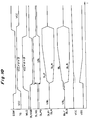
- Fig. 2 shows a waveform diagram illustrating the operation of the circuit in Fig. 1. The operation of a conventional DRAM will now be described with reference to Fig. 2.
- the sense operation starts when the sense starting signal SLNGB falls from “H” level to “L” level.
- the inverter 17 causes the sense amplifier activating signal SLNG to rise from “L” level to “H” level (VCC), and the sense amplifier activating signal SLPG falls from “H” level to “L” level (VSS). Therefore, both the PMOS 15 and the NMOS 16 are turned on and the sense amplifiers 13 and 14 are activated.
- the small potential difference between the nodes NA and NAB connected to the bit lines BL and BLB is sensed and amplified by the just-activated sense amplifiers 13 and 14 by charging and discharging the nodes NA and NAB through the PMOS 15 and NMOS 16, respectively.
- the object of the present invention is to provide a sense circuit which does not cause a sharp voltage drop on the power supply voltage.
- the sense circuit in a dynamic random access memory in which a plurality of memory arrays include a plurality of memory cells, a plurality memory cells in each of the plurality of memory arrays have respective piece of data, and the plurality of memory arrays share a voltage applied by a power supply in use for accessing of the piece of the data;
- the sense circuit comprises sense means for sensing a current which flows out of the memory cell corresponding to the piece of data upon accessing the piece of the data in the memory cell; amplification means for developing a specific voltage corresponding to the sensed current; and switching means for allowing a current in use for the development of the specific voltage to flow between the power supply and the amplification means in such a manner that the current therebetween does not cause the voltage applied to the plurality of the memory cells to sag.
- Fig. 1 shows the main circuit of a conventional DRAM.
- Fig. 2 shows a waveform diagram illustrating the operation of a conventional circuit.
- Fig. 3 shows the main circuit of the DRAM of a first embodiment of the present invention.
- Fig. 4 shows a waveform diagram illustrating the operation of the circuit of the first embodiment.
- Fig. 5 shows the main circuit of the DRAM of a second embodiment of the present invention.
- Fig. 6 shows a waveform diagram illustrating the operation of the circuit of the second embodiment.
- Fig. 7 shows the main circuit of the DRAM of a third embodiment of the present invention.
- Fig. 8 shows a waveform diagram illustrating the operation of the circuit of the third embodiment.
- Fig. 9 shows the main circuit of the DRAM of a fourth embodiment of the present invention.
- Fig. 10 shows a waveform diagram illustrating the operation of the circuit of the fourth embodiment.
- Fig. 11 shows the main circuit of the DRAM of a fifth embodiment of the present invention.
- Fig. 12 shows a waveform diagram illustrating the operation of the circuit of the fifth embodiment.
- Fig. 13 shows the main circuit of the DRAM of a sixth embodiment of the present invention.
- Fig. 14 shows a waveform diagram illustrating the operation of the circuit of the sixth embodiment.
- Fig. 3 shows the main circuit of the DRAM of a first embodiment of the present invention.
- each memory cell has the same structure and consists of a parallel-plate capacitor 21 and an NMOS 22.
- One electrode of the capacitor 21 is connected to the source electrode of the NMOS 22, while the other electrode of the capacitor is connected to a first reference potential VCP, which is the cell plate potential.
- the level of this first reference potential VCP is about midway between a first power potential VSS and a second power potential VCC, and is generated by a VCP generating circuit 23.
- the drain electrode of the NMOS 22 in the memory cell M1 shown in Fig. 3 is connected to a bit line BL, while the gate electrode (of the NMOS 22) is connected to a word line WL0.
- the drain electrode of the NMOS 27 in the memory cell M2 is connected to a bit line BLB, while the gate electrode (of the NMOS 27) is connected to a word line WL1.
- the bit lines BL and BLB that are output from the memory cell array 20 are connected to an equalizing circuit 25.
- the equalizing circuit 25 is used to supply the same potential level to the bit lines BL and BLB, and consists of NMOS's 25a and 25b, the source electrodes of which are connected to the second reference potential VBL for the purpose of pre-charging the bit lines.
- the drain electrodes of the NMOS's 25a and 25b are connected to the bit lines BL and BLB, respectively, and the gate electrodes (of the NMOS's 25a and 25b) are connected to the pre-charging control signal EQM.
- the level of the second reference potential VBL is about midway between the second power potential VCC and the first power potential VSS, and is generated by a VBL generating circuit 26.
- a sense circuit 30 is connected to the bit lines BL and BLB.
- bit lines BL and BLB are connected to sense amplifier nodes NA and NAB by NMOS's 31 and 32, respectively, which are transfer gates. Further, the gate electrodes of the NMOS's 31 and 32 are connected to the control signal TG. When the control signal TG becomes active, the NMOS's 31 and 32 are turned on. Consequently, the nodes NA and NAB become connected to the bit lines BL and BLB through the NMOS's 31 and 32, respectively.
- a sense amplifier 33 consisting of two NMOS's 33a and 33b, the source electrodes of which are connected to each other.
- a second sense amplifier 34 that consists of two PMOS's 34a and 34b, the source electrodes of which are connected to each other.
- the node NA is connected to the drain electrodes of the NMOS 33a and the PMOS 34a, and to the gate electrodes of the NMOS 33b and PMOS 34b.
- the node NAB is connected to the drain electrode of the NMOS 33b and PMOS 34b, and to the gate electrodes of the NMOS 33a and PMOS 34a.
- the source electrodes of the NMOS's 33a and 33b are connected to the drain electrode of NMOS 35, the source electrode of which is connected to the first power potential VSS.
- the source electrodes of the PMOS's 34a and 34b are connected to the drain electrode of PMOS 36, the source electrode of which is connected to the second power potential VCC.
- the sense circuit 30 has an activating signal generation circuit that generates the first activating signal SLNG and the second activating signal SLPG.
- the activating signal generation circuit consists of a first inverter 37 and a second inverter 38.
- the input signal of the inverter 37 is the sense starting signal SLNGB, which is one of the control signals, and the output signal of the inverter (37) is the first activating signal SLNG.
- the input signal of the inverter 38 is the first activating signal SLNG, and the output signal (of the inverter 38) is the second activating signal SLPG.
- the first and second activating signals SLNG and SLPG are logically complementary.
- the inverter 38 consists of a PMOS 38a and an NMOS 38b.
- the gate electrodes of the PMOS 38a and NMOS 38b are connected to the activating signal SLNG, while the drain electrodes of the PMOS 38a and NMOS 38b are connected together.
- the source electrode of the PMOS 38a is connected to the second power potential VCC.
- the source electrode of the NMOS 38b is connected to the second reference potential VBL, unlike in a conventional circuit.
- the output signal of the inverter 37 (the first activating signal SLNG) is provided to the gate of the NMOS 35, while the output signal of the inverter 38 (the second activating signal SLPG) is provided to the gate of the PMOS 36.
- Fig. 4 shows a waveform diagram illustrating the operation of the circuit in Fig. 3. The operation of the circuit of the first embodiment will now be described with reference to Fig. 4.
- the sense operation starts when the sense starting signal SLNGB falls from “H” level to “L” level.
- the inverter 37 causes the first activating signal SLNG to rise from “L” level to "H” level (VCC).
- the NMOS 38b is activated and the second activating signal SLPG falls from “H” level to “L” level.
- the “L” level of the second activating signal SLPG is the second reference potential VBL, which now flows through the NMOS 38b.
- both the NMOS 35, the input of which is the "H” level of the activating signal SLNG, and the PMOS 36, the input of which is the “L” level of the activating signal SLPG, are turned on, and the sense amplifiers 33 and 34 are activated.
- the small potential difference between the nodes NA and NAB connected to the bit lines BL and BLB is sensed and amplified by the activated sense amplifiers 33 and 34 by charging and discharging the nodes NA and NAB through the PMOS 36 and NMOS 35, respectively.
- the small potential difference between the bit lines BL and BLB becomes large enough to be memorized by the corresponding memory cell.
- the "L" level of the second activating signal SLPG which is the output of the inverter 38, is the second reference potential VBL (nearly (VSS+VCC)/2), and this second reference potential VBL is provided to the gate electrode of the PMOS 36. Accordingly, the following benefits (a), (b), and (c) are attained.
- Fig. 5 shows the main circuit of the DRAM of a second embodiment of the present invention.
- the naming conventions for the elements in Fig. 5 are the same as for those in Fig. 3.
- the DRAM circuit of the second embodiment like that of the first embodiment, has a memory cell array 20, an equalizing circuit 25, a VCP generating circuit 23, a VBL generating circuit 26, all of which are the same as those in the first embodiment, and a sense circuit 40, which differs from that in Fig. 3.
- the sense circuit 40 is connected to the bit lines BL and BLB.
- the bit lines BL and BLB are connected to the sense amplifier nodes NA and NAB by way of NMOS's 41 and 42, respectively, which are transfer gates. Additionally, there two sense amplifiers 43 and 44 between the nodes NA and NAB in the sense circuit 40.
- the first sense amplifier 43 consists of two NMOS's 43a and 43b, the source electrodes of which are connected to each other.
- the second sense amplifier 44 consists of two PMOS's 44a and 44b, the source electrodes of which are also connected to each other.
- the node NA is connected to the drain electrodes of the NMOS 43a and PMOS 44a, and to the gate electrodes of the NMOS 43b and PMOS 44b.
- the node NAB is connected to the drain electrodes of the NMOS 43b and PMOS 44b, and to the gate electrodes of the NMOS 43a and PMOS 44a.
- the source electrodes of the NMOS's 43a and 43b are connected to the drain electrode of NMOS 45, the source electrode of which is connected to the first power potential VSS.
- the source electrodes of the PMOS's 44a and 44b are connected to the drain electrode of PMOS 46, the source electrode of which is connected to the second power potential VCC.
- the sense circuit 40 has an activating signal generation circuit that generates a first activating signal SLNG and a second activating signal SLPG.
- the activating signal generation circuit consists of a first inverter 47 and a second inverter 48.
- the input signal of the inverter 47 is the sense starting signal SLNGB, which is one of the control signals, and the output signal (of the inverter 47) is the first activating signal SLNG.
- the input signal of the inverter 48 is the first activating signal SLNG, and the output signal (of the inverter 48) is the second activating signal SLPG.
- the first activating signal SLNG and the second activating signal SLPG are logically complementary.
- the inverter 48 consists of the PMOS's 48a and 48b.
- the gate electrodes of the PMOS 48a is connected to the first activating signal SLNG, while the gate electrode of the PMOS 48b is connected to the sense starting signal SLNGB.
- the drain electrodes of the PMOS 48a and PMOS 48b are connected together.
- the source electrode of the PMOS 48a is connected to the second power potential VCC.
- the source electrode of the PMOS 48b is connected to the second reference potential VBL.
- the output signal of the inverter 47 (the first activating signal SLNG) is provided to the gate of the NMOS 45, while the output signal of the inverter 48 (the second activating signal SLPG) is provided to the gate of the PMOS 46.
- Fig. 6 is a waveform diagram illustrating operation of the circuit in Fig. 5. The operation of the second embodiment will now be described with reference to Fig. 6.
- the DRAM behaviour of the second embodiment is fundamentally the same as that of the first embodiment.
- the NMOS's 25a and 25b in the equalizing circuit 25 are cut off when the pre-charging control signal EQM becomes "L".
- the NMOS's 41 and 42 are turned on, and the bit lines BL and BLB are connected to the nodes NA and NAB, respectively.
- the above behaviour is the same as that of the first embodiment.
- the sense operation starts when the sense starting signal SLNGB falls from “H” level to “L” level.
- the first activating signal SLNG is caused to rise from “L” level to "H” level (VCC) by the inverter 47.
- the PMOS 48b is turned on and the second activating signal SLPG falls from “H” level to “L” level.
- the “L” level of the second activating signal SLPG is the second reference potential VBL, which now flows through the PMOS 48b.
- both the NMOS 45, the input of which is the "H” level of the activating signal SLNG, and the PMOS 46, the input of which is the “L” level of the activating signal SLPG, are turned on, and the sense amplifiers 43 and 44 are activated.
- the small potential difference between the nodes NA and NAB connected to the bit lines BL and BLB is sensed and amplified by the activated sense amplifiers 43 and 44 by charging and discharging the nodes NA and NAB through the PMOS 46 and NMOS 45, respectively. Therefore the small potential difference between the bit lines BL and BLB becomes large enough to be memorized by the corresponding memory cell.
- an important aspect of the circuit structure of the second embodiment is that the "L" level of the second activating signal SLPG, which is set to the second reference potential VBL, is provided to the gate electrode of the PMOS 46. Consequently, the benefits (a), (b), and (c) of the first embodiment are also attained. Furthermore, the falling time of the second activating signal SLPG is one inverter stage faster than that of a conventional circuit. This is because the PMOS 48b of the inverter 48 is activated by the sense starting signal SLNGB (rather than by SLNG).
- Fig. 7 shows the main circuit of the DRAM of a third embodiment of the present invention.
- the naming conventions for the elements in Fig. 3, Fig. 5, and Fig. 7 are the same.
- the DRAM circuit of the third embodiment like that of the first and second embodiments, has a memory cell array 20, an equalizing circuit 25, a VCP generating circuit 23, a VBL generating circuit 26, all of which are the same as those in the first embodiment, and a sense circuit 50, which differs from that in Fig. 3 or Fig. 5.
- the sense circuit 50 is connected to the bit lines BL and BLB.
- the bit lines BL and BLB are connected to the sense amplifier nodes NA and NAB by way of NMOS's 51 and 52, respectively, which are transfer gates.
- NMOS's 51 and 52 respectively, which are transfer gates.
- the first sense amplifier 53 consists of two NMOS's 53a and 53b, the source electrodes of which are connected to each other.
- the second sense amplifier 54 consists of two PMOS's 54a and 54b, the source electrodes of which are connected to each other.
- the node NA is connected to the drain electrodes of the NMOS 53a and PMOS 54a, and to the gate electrodes of the NMOS 53b and PMOS 54b.
- the node NAB is connected to the drain electrodes of the NMOS 53b and PMOS 54b, and to the gate electrodes of the NMOS 53a and PMOS 54a.
- the source electrodes of the NMOS 53a and 53b are connected to the drain electrode of NMOS 55, the source electrodes of which is connected to the first power potential VSS.
- the source electrodes of the PMOS 54a and 54b are connected to the drain electrode of PMOS 56, the source electrodes of which is connected to the second power potential VCC.
- the sense circuit 50 which is different from that in the first and second embodiments, has an activating signal generation circuit that generates a first activating signal SLNG and a second activating signal SLPG.
- the activating signal generation circuit consists of a first inverter 57 and a second inverter 58.
- the input signal of the inverter 57 is the sense starting signal SLNGB, which is one of the control signals, and the output signal of the inverter 57 is the first activating signal SLNG.
- the input signal of the inverter 58 is the first activating signal SLNG and the output signal of the inverter 58 is the second activating signal SLPG.
- the first activating signal SLNG and the second activating signal SLPG are logically complementary.
- the inverter 58 consists of a PMOS 58a, a PMOS 58b and an NMOS 58c.
- the gate electrodes of the PMOS 58a and the NMOS 58c are connected to the first activating signal SLNG, while the gate electrode of the PMOS 58b is connected to the sense starting signal SLNGB.
- the drain electrodes of the PMOS 58a, PMOS 58b, and NMOS 58c are connected together.
- the source electrode of the PMOS 58a is connected to the second power potential VCC.
- the source electrodes of the PMOS 58b and NMOS 58c are connected to the second reference potential VBL.
- the output signal of the inverter 57 (the first activating signal SLNG) is provided to the gate of the NMOS 55, while the output signal of the inverter 58 (the second activating signal SLPG) is provided to the gate of the PMOS 56.
- Fig. 8 is a waveform diagram illustrating the operation of the circuit in Fig. 7. The operation of the circuit in Fig. 7 will now be described with reference to Fig. 8.
- the DRAM behaviour of the third embodiment is fundamentally the same as that of the first and second embodiments.
- the NMOS's 25a and 25b in the equalizing circuit 25 is cut off when the pre-charging control signal EQM becomes "L".
- the NMOS's 51 and 52 are turned on and the bit lines BL and BLB become connected to the nodes NA and NAB, respectively.
- the above behaviour is the same as that of the first and second embodiments.
- the sense operation starts when the sense starting signal SLNGB falls from "H" level to "L” level.
- the first activating signal SLNG is caused to rise from "L" level to "H” level (VCC) by the inverter 57.
- the PMOS 58b is turned on and the second activating signal SLPG falls from "H" level to "L” level.
- the NMOS 58c is also activated, though this happens after the activation of the PMOS 58b because of the propagation delay of the inverter 57.
- the activated NMOS 58c stabilizes the level of the second activating signal SLPG, and the "L" level of the second activating signal SLPG is fixed to the second reference potential level VBL.
- both the NMOS 55, the input of which is the "H” level of the activating signal SLNG, and the PMOS 56, the input of which is the “L” level of the activating signal SLPG, are turned on and the sense amplifiers 53 and 54 are activated.
- the small potential difference between the nodes NA and NAB connected to the bit lines BL and BLB is sensed and amplified by the activated sense amplifiers 53 and 54 by charging and discharging the nodes NA and NAB through the PMOS 56 and NMOS 55, respectively. Therefore the small potential difference between the bit lines BL and BLB becomes large enough to be memorized by the corresponding memory cell.
- an important aspect of the circuit structure of the third embodiment is that the "L" level of the second activating signal SLPG, which is set to the second reference potential VBL ((VSS+VCC)/2), is provided to the gate electrode of the PMOS 56. Consequently, the benefits (a) and (b) of the first and second embodiments are also attained.
- the falling time of the second activating signal SLPG is one inverter stage faster than that of a conventional circuit, since the PMOS 58b of the inverter 58 is activated by the sense starting signal SLNGB.
- the NMOS transistor 58c of the inverter 58 stabilizes the level of the second activating signal SLPG, and the "L" level of the second activating signal SLPG is fixed to the second reference potential level VBL.
- Fig. 9 shows the main circuit of the DRAM of a fourth embodiment of the present invention.
- the naming conventions for the elements in this embodiment are the same as those of the embodiments presented earlier (Fig. 3, Fig. 5, and Fig. 7).
- the electric potential of the second activating signal SLPG in the first embodiment is the second reference potential VBL
- the electric potential of the activating signal (SLPG) in this embodiment is the first reference potential VCP.
- the DRAM circuit of the fourth embodiment consists of a memory cell array 20, an equalizing circuit 25, a VCP generating circuit 23, a VBL generating circuit 26, and a sense circuit 60, to which the first reference potential VCP is provided.
- the sense circuit 60 which has almost same structure as the sense circuit in Fig. 3, is connected to the bit lines BL and BLB.
- the bit lines BL and BLB are connected to the sense amplifier nodes NA and NAB by NMOS's 61 and 62, respectively, which are transfer gates.
- the first sense amplifier 63 consists of two NMOS's 63a and 63b, the source electrodes of which are connected to each other.
- the second sense amplifier 64 consists of two PMOS's 64a and 64b, the source electrodes of which are connected to each other.
- the node NA is connected to the drain electrodes of the NMOS 63a and PMOS 64a, and to the gate electrodes of the NMOS 63b and PMOS 64b.
- the node NAB is connected to the drain electrodes of the NMOS 63b and PMOS 64b, and the gate electrodes of the NMOS 63a and PMOS 64a.
- the source electrodes of the NMOS's 63a and 63b are connected to the drain electrode of NMOS 65, the source electrode of which is connected to the first power potential VSS.
- the source electrodes of the PMOS's 64a and 64b are connected to the drain electrode of the PMOS 66, the source electrode of which is connected to the second power potential VCC.
- the sense circuit 60 has an activating signal generation circuit which generates a first activating signal SLNG and a second activating signal SLPG.
- the activating signal generation circuit consists of a first inverter 67 and a second inverter 68.
- the input signal of the inverter 67 is the sense starting signal SLNGB, which is one of the control signals, and the output signal of the inverter 67 is the first activating signal SLNG.
- the input signal of the inverter 68 is the first activating signal SLNG, and the output signal of the inverter 68 is the second activating signal SLPG.
- the first activating signal SLNG and the second activating signal SLPG are logically complementary.
- the inverter 68 consists of a PMOS 68a and an NMOS 68b.
- the gate electrodes of the PMOS 68a and NMOS 68b are connected to the activating signal SLNG, while the drain electrodes of the PMOS 68a and NMOS 68b are connected together.
- the source electrode of the PMOS 68a is connected to the second power potential VCC.
- the source electrode of the NMOS 68b is connected to the first reference potential VCP.
- the output signal of the inverter 67 (the first activating signal SLNG) is provided to the gate of the NMOS 65, while the output signal of the inverter 68 (the second activating signal SLPG) is provided to the gate of the PMOS 66.
- Fig. 10 is a waveform diagram illustrating the behaviour of the circuit in Fig. 9.
- the source electrode of the NMOS 68b in the inverter 68 is connected to the first reference potential VCP (instead of the second reference potential VBL), which is nearly (VSS+VCC)/2. Therefore, since the electric potential of the second activating signal SLPG is the same as that in Fig. 4, the operation of this circuit is the same as that described in the first embodiment.
- Fig. 11 shows the main circuit of the DRAM of a fifth embodiment of the present invention.
- the naming conventions for the elements are the same as those in Fig. 3, Fig. 5, Fig. 7 and Fig. 9. It is clear from the fourth embodiment that power noise reduction can be realized whether the first reference potential VCP or the second reference potential VBL is connected to the electric potential of the second activating signal.
- a connecting circuit 70 e.g., a transfer gate
- This circuit has a memory cell array 20, an equalizing circuit 25, a VCP generating circuit 23, and a VBL generating circuit 26, all of which are the same circuits found in the first through fourth embodiments.
- the connecting circuit 70 is used to connect the first reference potential VCP and the second reference potential VBL, which occurs when the connecting circuit 70 is activated.
- a sense circuit 80 is connected to the bit lines BL and BLB.
- the bit lines BL and BLB are connected to the sense amplifier nodes NA and NAB by way of NMOS 81 and 82, respectively, which are transfer gates.
- NMOS 81 and 82 are transfer gates.
- the first sense amplifier 83 consists of two NMOS's 83a and 83b, the source electrodes of which are connected to each other.
- the second sense amplifier 84 consists of two PMOS's 84a and 84b, the source electrodes of which are also connected to each other.
- the node NA is connected to the drain electrodes of the NMOS 83a and PMOS 84a, and to the gate electrodes of the NMOS 83b and PMOS 84b.
- the node NAB is connected to the drain electrodes of the NMOS 83b and PMOS 84b, and to the gate electrodes of the NMOS 83a and PMOS 84a.
- the source electrodes of the NMOS's 83a and 83b are connected to the drain electrode of NMOS 85, the source electrode of which is connected to the first power potential VSS.
- the source electrodes of the PMOS 84a and 84b are connected to the drain electrode of PMOS 86, the source electrode of which is connected to the second power potential VCC.
- the sense circuit 80 has an activating signal generation circuit which generates a first activating signal SLNG and a second activating signal SLPG.
- the activating signal generation circuit consists of a first inverter 87 and a second inverter 88.
- the input signal of the inverter 87 is the sense starting signal SLNGB, which is one of the control signals, and the output signal of the inverter 87 is the first activating signal SLNG.
- the input signal of the inverter 88 is the first activating signal SLNG, and the output signal of the inverter 88 is the second activating signal SLPG.
- the first activating signal SLNG and the second activating signal SLPG are logically complementary.
- the inverter 88 consists of a PMOS 88a and an NMOS 88b.
- the gate electrodes of the PMOS 88a and NMOS 88b are connected to the activating signal SLNG, while the drain electrodes of the PMOS 88a and NMOS 88b are connected together.
- the source electrode of the PMOS 88a is connected to the second power potential VCC.
- the source electrode of the NMOS 88b is connected to the first reference potential VCP and second reference potential VBL.
- the output signal of the inverter 87 (the first activating signal SLNG) is provided to the gate of the NMOS 85 while the output signal of the inverter 88 (the second activating signal SLPG) is provided to the gate of the PMOS 86.
- Fig. 12 is a waveform diagram illustrating the behaviour of the circuit in Fig. 11.
- the source electrode of the NMOS 88b in the inverter 88 is connected to the first reference potential VCP and to the second reference potential VBL, both of which are nearly (VSS+VCC)/2. Therefore, since the electric potential of the second activating signal SLPG is the same as that in Fig. 4, the operation of this circuit is the same as that of the first embodiment.
- the source electrode of the NMOS 88 is connected to both the first and second reference potentials VCP and VBL, the benefits (a), (b), and (c) of the first embodiment are attained.
- Fig. 13 shows the main circuit of the DRAM of a sixth embodiment of the present invention.
- the naming conventions for the elements are the same as for those in Fig. 3, Fig. 5, Fig. 7, Fig. 9 and Fig. 11.
- the electric potential of the second activating signal SLPG is either the first reference potential VCP or the second reference potential VBL.
- a source potential generating circuit 90 that outputs a third reference potential VX is introduced, and the "L" level of the second activating signal SLPG is this third reference potential VX (which is independent of the first and second reference potentials VCP and VBL).
- the DRAM circuit of the sixth embodiment has a memory cell array 20, an equalizing circuit 25, a VCP generating circuit 23, and a VBL generating circuit 26, which are the same circuits as those in the earlier embodiments.
- the sense circuit 100 has almost same structure as that in Fig. 1, and is connected to the bit lines BL and BLB.
- the bit lines BL and BLB are connected to the sense amplifier nodes NA and NAB by NMOS's 101 and 102, respectively, which are transfer gates. Additionally, there are two sense amplifiers 103 and 104 between the nodes NA and NAB in the sense circuit 100.
- the first sense amplifier 103 consists of two NMOS's 103a and 103b, the source electrodes of which are connected to each other, while the second sense amplifier 104 consists of two PMOS's 104a and 104b, the source electrodes of which are connected to each other.
- the node NA is connected to the drain electrodes of the NMOS 103a and PMOS 104a, and to the gate electrodes of the NMOS 103b and PMOS 104b.
- the node NAB is connected to the drain electrodes of the NMOS 103b and PMOS 104b, and to the gate electrodes of the NMOS 103a and PMOS 104a.
- the source electrodes of the NMOS 103a and 103b are connected to the drain electrode of NMOS 105, the source electrode of which is connected to the first power potential VSS.
- the source electrodes of the PMOS 104a and 104b are connected to the drain electrode of PMOS 106, the source electrode of which is connected to the second power potential VCC.
- the sense circuit 100 has an activating signal generation circuit which generates a first activating signal SLNG and a second activating signal SLPG.
- the activating signal generation circuit consists of a first inverter 107 and a second inverter 108.
- the input signal of the inverter 107 is the sense starting signal SLNGB, which is one of the control signals, while the output signal of the inverter 107 is the first activating signal SLNG.
- the input signal of the inverter 108 is the first activating signal SLNG, and the output signal of the inverter 108 is the second activating signal SLPG.
- the first activating signal SLNG and the second activating signal SLPG are logically complementary.
- the inverter 108 consists of a PMOS 108a and an NMOS 108b.
- the gate electrodes of the PMOS 108a and the NMOS 108b are connected to the activating signal SLNG, while the drain electrodes of the PMOS 108a and the NMOS 108b are connected together.
- the source electrode of the PMOS 108a is connected to the second power potential VCC.
- the source electrode of the NMOS 108b is connected to the third reference potential VX, which is supplied by the source potential generating circuit 90.
- the output signal of the inverter 107 (the first activating signal SLNG) is provided to the gate of the NMOS 105, while the output signal of the inverter 108 (the second activating signal SLPG) is provided to the gate of the PMOS 106.
- Fig. 14 shows a waveform diagram illustrating the behaviour of the circuit in Fig. 13.
- the source potential generating circuit 90 is introduced into the circuit of the sixth embodiment, and the source electrode of the NMOS 108b is connected to the third reference potential VX.
- the third reference potential VX can be changed independently of the first and second reference potentials VBL and VCP. Therefore, the DRAM circuit of the sixth embodiment can be realized by appropriate adjustments of the third reference potential level.
- the DRAM circuit of the sixth embodiment thus attains the benefits (a) and (b) of the first embodiment.
- the internal circuit structure for the memory cell array 20 or the equalizing circuit 25 can be changed to another circuit structure, and is therefore not limited to the structure described in the first through sixth embodiments.
- the sense circuit 60 in the fourth embodiment is connected to the first reference potential VCP (unlike the sense circuit 30 in the first embodiment, which is connected to the second reference potential VBL).
- the first reference potential VCP can likewise be applied to the sense circuits 40 and 60 in the second and third embodiments while attaining the same benefits.
- the active potential level of the second activating signal which activates the MOS transistors 36, 46, 56, 66, 86, and 106 in the respective activating signal generation circuits, is midway between the first and second power potentials. Therefore, the operating region of the MOS transistor, the input of which is the second activating signal with midway potential level, is different from that of a conventional circuit, the input of which is the second power potential.
- the conductive resistance of the MOS transistor in the present invention is higher than that of the MOS transistor in conventional circuits. Consequently, the peak current when charging and discharging the bit lines will be reduced, power noise will be decreased, and a decrease of operating margin of a peripheral circuit will be prevented.
Abstract
Description
Claims (4)
- The sense circuit in a dynamic random access memory in which a plurality of memory arrays include a plurality of memory cells, a plurality memory cells in each of the plurality of memory arrays have respective piece of data, the plurality of memory arrays share a voltage applied by a power supply in use for accessing of the piece of the data; the sense circuit comprising:sense means for sensing a current which flows out of the memory cell corresponding to the data upon accessing the piece of the data in the memory cell;amplification means for developing a specific voltage corresponding to the sensed current; andswitching means for allowing a current in use for the development of the specific voltage to flow between the power supply and the amplification means in such a manner that the current therebetween does not cause the voltage applied to the plurality of the memory cells to sag.
- The sense circuit as set forth in claim 1, further comprising voltage applying means for applying to the switching means such a voltage as to permit the switching means to adjust the amount of the current flowing into the amplification means.
- The sense circuit as set forth in claim 2, further comprising reduction means for reducing a period necessary for applying the voltage into the switching means by the voltage applying means.
- A dynamic random access memory including:a plurality of memory cells in an array,a power supply which provides a voltage shared by the plurality of memory cells for accessing data stored in the cells of the array individually, anda sensing circuit for each said memory cell, comprising:sense means for sensing a current which flows out of the memory cell corresponding to the stored data, when accessed,amplification means for developing an output voltage corresponding to the sensed current; and characterised byswitching means for allowing a current to flow from the power supply to the amplification means to produce said output voltage in such a manner that the voltage applied to the plurality of the memory cells does not drop.
Applications Claiming Priority (3)
| Application Number | Priority Date | Filing Date | Title |
|---|---|---|---|
| JP19500496A JP3672384B2 (en) | 1996-07-24 | 1996-07-24 | Sense circuit |
| JP19500496 | 1996-07-24 | ||
| JP195004/96 | 1996-07-24 |
Publications (3)
| Publication Number | Publication Date |
|---|---|
| EP0821364A2 true EP0821364A2 (en) | 1998-01-28 |
| EP0821364A3 EP0821364A3 (en) | 1999-03-10 |
| EP0821364B1 EP0821364B1 (en) | 2003-11-19 |
Family
ID=16333941
Family Applications (1)
| Application Number | Title | Priority Date | Filing Date |
|---|---|---|---|
| EP97305400A Expired - Lifetime EP0821364B1 (en) | 1996-07-24 | 1997-07-18 | Sense circuit |
Country Status (7)
| Country | Link |
|---|---|
| US (1) | US5949729A (en) |
| EP (1) | EP0821364B1 (en) |
| JP (1) | JP3672384B2 (en) |
| KR (1) | KR100338271B1 (en) |
| CN (1) | CN1191587C (en) |
| DE (1) | DE69726225T2 (en) |
| TW (1) | TW328591B (en) |
Cited By (1)
| Publication number | Priority date | Publication date | Assignee | Title |
|---|---|---|---|---|
| CN110189782A (en) * | 2018-02-22 | 2019-08-30 | 瑞萨电子株式会社 | Semiconductor devices |
Families Citing this family (17)
| Publication number | Priority date | Publication date | Assignee | Title |
|---|---|---|---|---|
| US5959916A (en) * | 1998-02-06 | 1999-09-28 | International Business Machines Corporation | Write driver and bit line precharge apparatus and method |
| US6128236A (en) * | 1998-12-17 | 2000-10-03 | Nippon Steel Semiconductor Corp. | Current sensing differential amplifier with high rejection of power supply variations and method for an integrated circuit memory device |
| US6198677B1 (en) * | 1998-12-29 | 2001-03-06 | International Business Machines Corporation | Boosted sensing ground circuit |
| KR100361862B1 (en) | 1998-12-30 | 2003-02-20 | 주식회사 하이닉스반도체 | Semiconductor memory device and sensing current reduction method |
| US6535415B2 (en) * | 1999-02-22 | 2003-03-18 | Hitachi, Ltd. | Semiconductor device |
| JP2000243085A (en) * | 1999-02-22 | 2000-09-08 | Hitachi Ltd | Semiconductor device |
| US6236605B1 (en) * | 1999-03-26 | 2001-05-22 | Fujitsu Limited | Semiconductor integrated circuit and semiconductor memory device including overdriving sense amplifier |
| JP2001084767A (en) * | 1999-08-30 | 2001-03-30 | Internatl Business Mach Corp <Ibm> | Sense amplifier |
| JP4366858B2 (en) * | 2000-09-18 | 2009-11-18 | ソニー株式会社 | MOS transistor circuit |
| JP4032039B2 (en) * | 2004-04-06 | 2008-01-16 | 株式会社東芝 | Semiconductor memory device |
| KR100702004B1 (en) * | 2004-08-02 | 2007-03-30 | 삼성전자주식회사 | Semiconductor memory device and bit line sensing method of the same |
| JP4411616B2 (en) * | 2006-07-24 | 2010-02-10 | エルピーダメモリ株式会社 | Semiconductor memory device and control method thereof |
| KR20130068482A (en) * | 2011-12-15 | 2013-06-26 | 에스케이하이닉스 주식회사 | Semiconductor memory apparatus |
| FR3017897B1 (en) * | 2014-02-21 | 2019-09-27 | I.T.H.P.P | ROTARY DRILLING SYSTEM BY ELECTRIC DISCHARGES |
| KR20160069147A (en) * | 2014-12-08 | 2016-06-16 | 에스케이하이닉스 주식회사 | Data sense amplifier and memory device including the same |
| US10236036B2 (en) * | 2017-05-09 | 2019-03-19 | Micron Technology, Inc. | Sense amplifier signal boost |
| US10566036B2 (en) | 2018-06-15 | 2020-02-18 | Micron Technology, Inc. | Apparatuses and method for reducing sense amplifier leakage current during active power-down |
Citations (2)
| Publication number | Priority date | Publication date | Assignee | Title |
|---|---|---|---|---|
| US5267203A (en) * | 1991-07-31 | 1993-11-30 | Samsung Electronics Co., Ltd. | Sense amplifier control circuit of a semiconductor memory device |
| US5508965A (en) * | 1993-09-14 | 1996-04-16 | Fujitsu Limited | Semiconductor memory device |
Family Cites Families (7)
| Publication number | Priority date | Publication date | Assignee | Title |
|---|---|---|---|---|
| JPS61158094A (en) * | 1984-12-28 | 1986-07-17 | Toshiba Corp | Sense amplifier drive circuit of dynamic memory |
| JPH0752670B2 (en) * | 1987-10-14 | 1995-06-05 | キヤノン株式会社 | Electroluminescent device and manufacturing method thereof |
| JPH0574156A (en) * | 1991-09-13 | 1993-03-26 | Sumitomo Metal Ind Ltd | Semiconductor memory circuit |
| JPH06150646A (en) * | 1992-11-13 | 1994-05-31 | Nec Corp | Semiconductor memory |
| JPH06302189A (en) * | 1993-02-22 | 1994-10-28 | Toshiba Corp | Semiconductor storage |
| JPH06309869A (en) * | 1993-04-28 | 1994-11-04 | Oki Electric Ind Co Ltd | Semiconductor storage device |
| US5539701A (en) * | 1994-08-05 | 1996-07-23 | Nippon Steel Corporation | Sense circuit for semiconductor memory devices |
-
1996
- 1996-07-24 JP JP19500496A patent/JP3672384B2/en not_active Expired - Fee Related
-
1997
- 1997-06-12 TW TW086108069A patent/TW328591B/en active
- 1997-07-18 EP EP97305400A patent/EP0821364B1/en not_active Expired - Lifetime
- 1997-07-18 DE DE69726225T patent/DE69726225T2/en not_active Expired - Fee Related
- 1997-07-21 US US08/897,645 patent/US5949729A/en not_active Expired - Fee Related
- 1997-07-23 KR KR1019970034494A patent/KR100338271B1/en not_active IP Right Cessation
- 1997-07-24 CN CNB971153558A patent/CN1191587C/en not_active Expired - Fee Related
Patent Citations (2)
| Publication number | Priority date | Publication date | Assignee | Title |
|---|---|---|---|---|
| US5267203A (en) * | 1991-07-31 | 1993-11-30 | Samsung Electronics Co., Ltd. | Sense amplifier control circuit of a semiconductor memory device |
| US5508965A (en) * | 1993-09-14 | 1996-04-16 | Fujitsu Limited | Semiconductor memory device |
Cited By (1)
| Publication number | Priority date | Publication date | Assignee | Title |
|---|---|---|---|---|
| CN110189782A (en) * | 2018-02-22 | 2019-08-30 | 瑞萨电子株式会社 | Semiconductor devices |
Also Published As
| Publication number | Publication date |
|---|---|
| DE69726225T2 (en) | 2004-08-19 |
| KR980011418A (en) | 1998-04-30 |
| EP0821364B1 (en) | 2003-11-19 |
| JP3672384B2 (en) | 2005-07-20 |
| KR100338271B1 (en) | 2002-07-18 |
| CN1172329A (en) | 1998-02-04 |
| TW328591B (en) | 1998-03-21 |
| EP0821364A3 (en) | 1999-03-10 |
| CN1191587C (en) | 2005-03-02 |
| DE69726225D1 (en) | 2003-12-24 |
| JPH1040681A (en) | 1998-02-13 |
| US5949729A (en) | 1999-09-07 |
Similar Documents
| Publication | Publication Date | Title |
|---|---|---|
| EP0821364B1 (en) | Sense circuit | |
| EP1349170B1 (en) | Sense amplifying circuit | |
| US4743784A (en) | Sense amplifier circuit | |
| KR0166505B1 (en) | Dram and sense amplifier array using separating internal power voltages | |
| US6201378B1 (en) | Semiconductor integrated circuit | |
| US6104655A (en) | Semiconductor storage device | |
| US5416371A (en) | Sense system for dynamic random access memory | |
| US6222780B1 (en) | High-speed SRAM having a stable cell ratio | |
| US5148399A (en) | Sense amplifier circuitry selectively separable from bit lines for dynamic random access memory | |
| KR0140175B1 (en) | Sense amplifier in memory device | |
| US6914836B2 (en) | Sense amplifier circuits using a single bit line input | |
| JP3359567B2 (en) | Semiconductor memory device having charge amplification bit line sense amplifier | |
| US5835403A (en) | Multiplication of storage capacitance in memory cells by using the Miller effect | |
| US5018105A (en) | Semiconductor memory device | |
| US5777934A (en) | Semiconductor memory device with variable plate voltage generator | |
| JPH0532839B2 (en) | ||
| US6490211B2 (en) | Random access memory device | |
| US5995410A (en) | Multiplication of storage capacitance in memory cells by using the Miller effect | |
| JP3723615B2 (en) | Dynamic semiconductor memory device | |
| US6181623B1 (en) | Semiconductor MOS/BIPOLAR composite transistor and semiconductor memory device using the same | |
| JP2555156B2 (en) | Dynamic RAM | |
| EP0318094B1 (en) | Integrated memory circuit with on-chip supply voltage control | |
| KR100291747B1 (en) | Precharge equalizer circuit | |
| JPS62165787A (en) | Semiconductor memory device | |
| US6806550B2 (en) | Evaluation configuration for semiconductor memories |
Legal Events
| Date | Code | Title | Description |
|---|---|---|---|
| PUAI | Public reference made under article 153(3) epc to a published international application that has entered the european phase |
Free format text: ORIGINAL CODE: 0009012 |
|
| AK | Designated contracting states |
Kind code of ref document: A2 Designated state(s): DE FR GB NL |
|
| AX | Request for extension of the european patent |
Free format text: AL;LT;LV;RO;SI |
|
| PUAL | Search report despatched |
Free format text: ORIGINAL CODE: 0009013 |
|
| AK | Designated contracting states |
Kind code of ref document: A3 Designated state(s): AT BE CH DE DK ES FI FR GB GR IE IT LI LU MC NL PT SE |
|
| AX | Request for extension of the european patent |
Free format text: AL;LT;LV;RO;SI |
|
| 17P | Request for examination filed |
Effective date: 19990811 |
|
| AKX | Designation fees paid |
Free format text: DE FR GB NL |
|
| 17Q | First examination report despatched |
Effective date: 20020314 |
|
| GRAH | Despatch of communication of intention to grant a patent |
Free format text: ORIGINAL CODE: EPIDOS IGRA |
|
| GRAS | Grant fee paid |
Free format text: ORIGINAL CODE: EPIDOSNIGR3 |
|
| GRAA | (expected) grant |
Free format text: ORIGINAL CODE: 0009210 |
|
| AK | Designated contracting states |
Kind code of ref document: B1 Designated state(s): DE FR GB NL |
|
| REG | Reference to a national code |
Ref country code: GB Ref legal event code: FG4D |
|
| REF | Corresponds to: |
Ref document number: 69726225 Country of ref document: DE Date of ref document: 20031224 Kind code of ref document: P |
|
| ET | Fr: translation filed | ||
| PLBE | No opposition filed within time limit |
Free format text: ORIGINAL CODE: 0009261 |
|
| STAA | Information on the status of an ep patent application or granted ep patent |
Free format text: STATUS: NO OPPOSITION FILED WITHIN TIME LIMIT |
|
| 26N | No opposition filed |
Effective date: 20040820 |
|
| PGFP | Annual fee paid to national office [announced via postgrant information from national office to epo] |
Ref country code: GB Payment date: 20060712 Year of fee payment: 10 |
|
| PGFP | Annual fee paid to national office [announced via postgrant information from national office to epo] |
Ref country code: DE Payment date: 20060713 Year of fee payment: 10 |
|
| PGFP | Annual fee paid to national office [announced via postgrant information from national office to epo] |
Ref country code: NL Payment date: 20060716 Year of fee payment: 10 |
|
| PGFP | Annual fee paid to national office [announced via postgrant information from national office to epo] |
Ref country code: FR Payment date: 20060719 Year of fee payment: 10 |
|
| GBPC | Gb: european patent ceased through non-payment of renewal fee |
Effective date: 20070718 |
|
| NLV4 | Nl: lapsed or anulled due to non-payment of the annual fee |
Effective date: 20080201 |
|
| PG25 | Lapsed in a contracting state [announced via postgrant information from national office to epo] |
Ref country code: NL Free format text: LAPSE BECAUSE OF NON-PAYMENT OF DUE FEES Effective date: 20080201 Ref country code: DE Free format text: LAPSE BECAUSE OF NON-PAYMENT OF DUE FEES Effective date: 20080201 |
|
| PG25 | Lapsed in a contracting state [announced via postgrant information from national office to epo] |
Ref country code: GB Free format text: LAPSE BECAUSE OF NON-PAYMENT OF DUE FEES Effective date: 20070718 |
|
| REG | Reference to a national code |
Ref country code: FR Ref legal event code: ST Effective date: 20080331 |
|
| PG25 | Lapsed in a contracting state [announced via postgrant information from national office to epo] |
Ref country code: FR Free format text: LAPSE BECAUSE OF NON-PAYMENT OF DUE FEES Effective date: 20070731 |