JP3667920B2 - IC card - Google Patents
IC card Download PDFInfo
- Publication number
- JP3667920B2 JP3667920B2 JP3798097A JP3798097A JP3667920B2 JP 3667920 B2 JP3667920 B2 JP 3667920B2 JP 3798097 A JP3798097 A JP 3798097A JP 3798097 A JP3798097 A JP 3798097A JP 3667920 B2 JP3667920 B2 JP 3667920B2
- Authority
- JP
- Japan
- Prior art keywords
- data
- card
- memory
- response
- display
- Prior art date
- Legal status (The legal status is an assumption and is not a legal conclusion. Google has not performed a legal analysis and makes no representation as to the accuracy of the status listed.)
- Expired - Fee Related
Links
Images


Classifications
-
- G—PHYSICS
- G06—COMPUTING; CALCULATING OR COUNTING
- G06K—GRAPHICAL DATA READING; PRESENTATION OF DATA; RECORD CARRIERS; HANDLING RECORD CARRIERS
- G06K19/00—Record carriers for use with machines and with at least a part designed to carry digital markings
- G06K19/06—Record carriers for use with machines and with at least a part designed to carry digital markings characterised by the kind of the digital marking, e.g. shape, nature, code
- G06K19/067—Record carriers with conductive marks, printed circuits or semiconductor circuit elements, e.g. credit or identity cards also with resonating or responding marks without active components
- G06K19/07—Record carriers with conductive marks, printed circuits or semiconductor circuit elements, e.g. credit or identity cards also with resonating or responding marks without active components with integrated circuit chips
- G06K19/077—Constructional details, e.g. mounting of circuits in the carrier
- G06K19/07701—Constructional details, e.g. mounting of circuits in the carrier the record carrier comprising an interface suitable for human interaction
- G06K19/07703—Constructional details, e.g. mounting of circuits in the carrier the record carrier comprising an interface suitable for human interaction the interface being visual
-
- G—PHYSICS
- G06—COMPUTING; CALCULATING OR COUNTING
- G06K—GRAPHICAL DATA READING; PRESENTATION OF DATA; RECORD CARRIERS; HANDLING RECORD CARRIERS
- G06K19/00—Record carriers for use with machines and with at least a part designed to carry digital markings
- G06K19/06—Record carriers for use with machines and with at least a part designed to carry digital markings characterised by the kind of the digital marking, e.g. shape, nature, code
- G06K19/067—Record carriers with conductive marks, printed circuits or semiconductor circuit elements, e.g. credit or identity cards also with resonating or responding marks without active components
- G06K19/07—Record carriers with conductive marks, printed circuits or semiconductor circuit elements, e.g. credit or identity cards also with resonating or responding marks without active components with integrated circuit chips
- G06K19/073—Special arrangements for circuits, e.g. for protecting identification code in memory
Landscapes
- Engineering & Computer Science (AREA)
- Computer Hardware Design (AREA)
- Microelectronics & Electronic Packaging (AREA)
- Physics & Mathematics (AREA)
- General Physics & Mathematics (AREA)
- Theoretical Computer Science (AREA)
- Computer Security & Cryptography (AREA)
- General Engineering & Computer Science (AREA)
- Credit Cards Or The Like (AREA)
- Techniques For Improving Reliability Of Storages (AREA)
Description
【0001】
【発明の属する技術分野】
本発明は、ICカードに関し、特に、データ通信における応答状態を表示することが可能なICカードに関するものである。
【0002】
【従来の技術】
従来より、外部に設置された質問器との間でデータ通信を行なうICカードがある。
【0003】
図6は、従来のICカード300の基本的な構成を概略的に示したブロック図である。ここに示した従来のICカード300は、信号重畳方式の非接触型のICカードであり、図示しない質問器から受ける1つ、または2つ以上の周波数の信号を使用して、電力の供給と情報の送受信とを行なう。
【0004】
図6における従来のICカード300は、1つの周波数を使用するICカードの一例であり、同調回路15、整流回路16、増幅復調回路17、変調増幅回路18、およびSP/PS変換回路19を備える。
【0005】
同調回路15は、アンテナとして機能するコイルLと、コンデンサCとを備える。整流回路16は、同調回路15で受信した信号を整流して、電力を生成し、ICカード300の各部に供給する。一方、増幅復調回路17は、同調回路15で受けた質問器からの情報Qを増幅して、復調する。増幅復調回路17から出力される信号は、SP/PS変換回路19でSP変換される。
【0006】
図6を参照して、さらに従来のICカード300は、主制御回路11と、メモリ10とを備える。
【0007】
主制御回路11は、SP/PS変換回路19から出力された信号を処理する。主制御回路11から出力された保持すべきデータは、データ保持用のメモリ10に記憶(保持)される。
【0008】
また、主制御回路11は、質問器から受けた情報Qの内容に応じて、指定されたメモリ10の領域からデータを読出し、これに基づき返答情報Aを生成する。返答情報Aは、SP/PS変換回路19でPS変換された後に、変調増幅回路18で処理され、アンテナLから質問器に送信される。
【0009】
【発明が解決しようとする課題】
ところで、上述のような従来のICカード300の応答状態の確認は、すべて図示しない質問器側で行なうこととしていため、従来のICカード300には、応答状態を確認する機能が備えられていなかった。
【0010】
したがって、ICカード300を使用しているユーザ側は、ICカード300の内部で何が起こっているか、どのような状態であるかを知ることができないという問題があった。
【0011】
例えば、複数のICカード300が、同時、もしくは時間間隔を開けず順次にデータ通信を行なった場合であって、質問器側でいずれかのICカード300からの応答の異常を検知した場合であっても、ユーザ側は、どのICカード300がデータ通信の異常を起こしたのか解らないという問題があった。
【0012】
これでは、質問器および応答器(ICカード)を含めたシステム全体の信頼性を確保することが困難となる。
【0013】
そこで、本発明は、かかる問題を解決するためになされたものであり、その目的は、データ通信における応答状態を外部表示することができるICカードを提供することにある。
【0014】
さらに、もう一つの目的は、データ通信における応答状態を一定期間持続的に表示することができるICカードを提供することにある。
【0015】
【課題を解決するための手段】
この発明によれば、ICカードは、外部から受けた第1のデータに応答してデータ通信を行なうICカードであって、第1のデータを記憶する第1の記憶手段と、第1のデータが第1の記憶手段に書込まれる前に第1の記憶手段に記憶されている第2のデータを待避させて記憶する第2の記憶手段と、第1のデータの受信および応答を制御する制御手段と、制御手段からの指示を受けてデータ通信の応答状態を表示する表示手段とを備え、制御手段は、第1の記憶手段への第1のデータの書込状態が正常であるか否かを判定する判定手段と、第1のデータの書込状態が異常のとき、第2の記憶手段に待避した第2のデータを用いて第1の記憶手段の内容を復旧する復旧手段とを含み、表示手段は、判定手段の判定結果が正常判定のとき、応答状態が正常であると表示し、判定手段の判定結果が異常判定であって、かつ、復旧手段により第1の記憶手段の内容が復旧されたとき、第1の記憶手段の内容が復旧されたことを表示し、判定手段の判定結果が異常判定であって、かつ、復旧手段により第1の記憶手段の内容の復旧ができなかったとき、応答状態が異常であると表示する。
【0019】
好ましくは、ICカードは、表示手段における表示を所定期間持続させるため、表示手段に一定期間電力を供給する電力供給手段をさらに備える。
【0020】
好ましくは、表示手段は、LCDまたはLEDのいずれかを含む。
【0021】
好ましくは、電力供給手段は、コンデンサを含む。
【0022】
好ましくは、電力供給手段は、電池を含む。
【0023】
好ましくは、電力供給手段は、太陽電池を含む。
【0025】
【発明の実施の形態】
[実施の形態1]
本発明の実施の形態1は、ICカードにおいて、表示機能を備え、データ保持用メモリのデータの書込み状態に基づき、データ通信におけるICカードの応答状態を外部表示することを可能としたものである。
【0026】
図1は、本発明の実施の形態1におけるICカ−ド100の要部の構成を示したブロック図であり、残りの部分については、図6に示した従来のICカード300の構成(但し、メモリ10を除く)と共通するので、その図示および説明は省略する。なお、本発明が適用されるICカードは、接触型ICカードであっても、非接触型ICカードであっても構わない。
【0027】
図1に示すICカ−ド100が、従来のICカード300と異なる点は以下にある。まず、メモリ10に代えて、データ保持用不揮発性メモリ2(以下、データ保持用メモリ2と呼ぶ)と、データ保護用不揮発性メモリ3(以下、データ保護用メモリ3と呼ぶ)とを備えること、そして、データ保持用メモリ2のデータの書込み状態を判定する異常判定回路1を備えること、さらに応答状態を表示する応答状態表示器7と応答状態表示器7に電力を一定期間供給する電力供給回路8とを備えることにある。
【0028】
図1を参照して、本発明の実施の形態1におけるICカード100の構成について説明する。
【0029】
レジスタ4は、今回のデータ通信で受信した保持すべきデータDAを図6に示した主制御回路11から受ける。なお、レジスタ4は、SRAMで構成しても構わない。データライトバッファ5は、レジスタ4のデータをデータ保持用メモリ2に書込むための回路である。アドレスデコーダ6は、データの読出し/書込み動作を行なうデータ保持用メモリ2の領域を指定する回路である。
【0030】
データ保持用メモリ2は、レジスタ4からデータDAを受けて、これを記憶する。図1を参照して、本発明の実施の形態1のデータ保持用メモリ2は、主制御回路11の制御に基づき、領域B1、B2、…、BNのいずれかに、1回のデータ通信で受信したデータDAを記憶するものとする。データ保持用メモリ2として、不揮発性のもの、たとえば、フラッシュメモリが用いられる。
【0031】
なお、本発明の実施の形態1におけるICカード100は、データ保持用メモリ2に記憶されているデータに基づき、データ通信処理を行なう。したがって、データ保持用メモリ2のデータに異常がある場合、データ通信で異常が発生する。
【0032】
データ保護用メモリ3は、データ保持用メモリ2に記憶されているデータを待避するメモリであって、データ保持用メモリ2のデータが破壊等された場合にデータ復旧を行なうために用いられる。図1を参照して、本発明の実施の形態1のデータ保護用メモリ3は、1回のデータ通信で受けるデータDAを記憶するための容量(領域B1,B2, …,もしくはBNの各容量以上)を備えるものとする。データ保護用メモリ3として、不揮発性のもの、例えば、フラッシュメモリが用いられる。
【0033】
なお、データ保護用メモリ3に書込むデータは、データ保持用メモリ2に記憶されている内容と一対一に対応が取れていればよく、例えば、データ保持用メモリ2のデータを反転したものであってもよい。
【0034】
異常判定回路1は、主制御回路11の指示のもと、データ保持用メモリ2のデータの書込み状態を判定して、これを状態判断用フラグFLGに記録して出力する。例えば、データ書込み時に電源異常が発生した場合、データ化けが起こることから、本発明の実施の形態1の異常判定回路1は、ICカード100を動作させる電源の状態に応じて、データ保持用メモリ2の書き込み状態を判定するものとする。
【0035】
状態判断用フラグFLGは、後述するように、データの処理状態に応じてその値が更新される。データ保持用メモリ2に保持すべきデータDAが記憶された場合は、状態判断用フラグFLGは初期化(データ書込み状態が正常と判定される)される。一方、データ保持用メモリ2にデータDAを書込む途中でデータに異常が発生した場合には、それ以降の処理にかかわらず、状態判断用フラグFLGは初期化されず、異常が発生した時点での値を保持する(データ書込み状態が異常と判定される)。
【0036】
なお、状態判断用のフラグFLGの値は、次のデータ通信処理まで保持される。状態判断用フラグFLGの一例として、不揮発性のメモリで構成するものが挙げられる。
【0037】
応答状態表示器7は、主制御回路11の指示を受けて、ICカード100の応答状態に関する表示を行なう。具体的には、状態判断用フラグFLGに応じて以下の内容を表示する。第1に、データ保持用メモリ2のデータ書込み状態が正常である場合には、正常な応答が完了したことを示す表示(正常通信完了表示)を行なう。第2に、データ保持用メモリ2のデータ書込み状態が異常であったが、データ保護用メモリ3のデータを用いてデータ復旧ができた場合には、データが復旧されたことを示す表示(データ復旧表示)を行なう。第3に、データ保持用メモリ2の書込み状態が異常であって、復旧するためのデータがデータ保護用メモリ3に存在しない場合には、応答が異常であったことを示す表示(通信異常表示)を行なう。
【0038】
電力供給回路8は、応答状態表示器7に一定期間電力を供給する回路である。応答状態表示器7は、この電力供給回路8からの電力の供給を受けて、応答状態を所定の期間持続して表示する。電力供給回路8は、図6に示した整流回路16から電流の供給を受ける大容量のコンデンサで構成するもの、その他、蓄電池を含むもの、太陽電池を含むもの等が挙げられる。
【0039】
続いて、本発明の実施の形態1におけるICカード100の動作について説明する。
【0040】
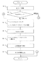
図2〜図3は、本発明の実施の形態1におけるICカ−ド100のデータ保持および復旧に関する動作を説明するためのフロー図の一例である。ここでは、状態判断用フラグFLGは、0もしくは1の値をとり、データ書込み状態が正常である場合には0に初期化されるものとする。
【0041】
図2〜図3を参照して、ICカード100のデータ保持、データ復旧動作、および応答状態の表示について説明する。
【0042】
ステップS1において、ICカードが起動する。
ステップS2において、状態判断用フラグFLGをチェックして、データ保持用メモリ2にデータが正常に書込まれているか(=0)否かを調べる。
【0043】
先ず、状態判断用フラグFLGが0、すなわちデータ保持用メモリ2のデータ書込み状態が正常である場合について説明する。
【0044】
なお、特に図示しないが、以下に示すステップS3〜ステップS5の処理中であって、データ保持用メモリ2へ書込が行なわれる期間以外は、ICカード100は、データ保持用メモリ2のデータを用いてデータ通信を行なっている。
【0045】
ステップS3では、レジスタ4にデータDAを入力する。そして、データ保持用メモリ2の領域B1のデータを読出して、データ保護用メモリ3に待避する(書込む)。ステップS4では、状態判断用フラグFLGを1(データ保持用メモリ2の領域B1のデータをデータ保護用メモリ3に待避した状態)に設定しておく。ステップS5では、レジスタ4に書込まれているデータDAを、データ保持用メモリ2の領域B1に書込む。
【0046】
ステップS5の処理(データ保持用メモリ2にデータDAを書込んだ状態)が終了した後は、ステップS6において、応答状態表示器7が、正常通信完了表示を行なう。そして、ステップS7において、状態判断用フラグFLGを初期化(=0)する。
【0047】
続いて、状態判断用フラグFLGが1、すなわちデータ保持用メモリ2のデータ書込み状態が異常である場合について説明する。
【0048】
なお、特に図示しないが、以下に説明する処理は、ICカード100が起動を開始してからデータ保持用メモリ2へのアクセスが開始されるまでの間に行なわれる。
【0049】
ステップS8ではデータ保持用メモリ2のデータを復旧するために必要なデータが、データ保護用メモリ3に存在するか否かを調べる。復旧用のデータが存在しない場合(例えば、初回の通信時には、データ保護用メモリ3にデータが存在しない)には、通信異常が発生することになるので、ステップS12において、応答状態表示器7が、通信異常表示を行なう。
【0050】
一方、復旧用のデータが存在した場合には、ステップS9において、応答状態表示器7が、データ復旧表示を行なう。そして、ステップS10において、データ保護用メモリ3に待避したデータを読出して、これをデータ保持用メモリ2の領域B1に書込む。この結果、通信異常の原因となるデータが破棄され、データ保持用メモリ2に正常なデータが書込まれる(復旧する)。ステップS10での復旧処理が終了した後は、ステップS11において、状態判断用フラグFLGを初期化(=0)する。そして、ステップS11で正常状態になった後は、上記に説明したステップS3〜S6の処理を行なう。
【0051】
図4は、本発明の実施の形態1におけるICカード100の外観構成を示す図である。図4の(a)に示すように、応答状態表示器7の一例として、LED(図4(a)におけるL1、L2、L3)を用いたものが挙げられる。例えば、図4におけるL1、L2、L3を、それぞれ正常通信完了表示、データ復旧表示、通信異常表示に対応させることができる。また、2色のLEDを用いることにより、正常通信表示、通信異常表示を視覚的に認識され易いように表示することもできる。
【0052】
また、表示内容としては、上記に説明したものに限られず、何らかの通信内容を表示するもの(図4(b)におけるL4、L5、L6、L7)であってもよい。
【0053】
その他、応答状態表示器7としては、LCDを用いたもの、また図4の(c)に示すように、LCD(図4(c)におけるL8)とLED(図4(c)におけるL1、L2)とを共に使用したものが挙げられる。
【0054】
以上のように、ICカード100は、表示機能を備え、さらにデータ保持用メモリ2のデータの書込み状態を判定して、その判定結果を用いることにより、データ通信におけるICカード100の応答状態を外部表示することができる。
【0055】
[実施の形態2]
本発明の実施の形態2は、ICカードにおいて、データ保持用のメインメモリ、もしくはデータ保持用のサブメモリを用いたデータ通信におけるICカードの応答状態を外部表示するものである。
【0056】
本発明の実施の形態2においては、電源異常のみならず、外部からの応力や、静電気などが原因となって起こるデータの変化を検知する。
【0057】
図5は、本発明の実施の形態2におけるICカ−ド200の要部の構成を示したブロック図であり、残りの部分については、図6に示した従来のICカード300の構成(但し、メモリ10を除く)と共通するので、その図示および説明は省略する。なお、本発明が適用されるICカードは、接触型ICカードであっても、非接触型ICカードであっても構わない。
【0058】
図5に示すICカ−ド200が、従来のICカード300と異なる主な点は以下にある。まず、メモリ10に代えて、データ保持用不揮発性メインメモリ(以下、メインメモリと呼ぶ)20と、データ保持用不揮発性サブメモリ(以下、サブメモリと呼ぶ)21とを備えこと、そして、メインメモリ20、サブメモリ21の誤り検出を行なう誤り検出回路22、23を備えること、さらに応答状態を表示する応答状態表示器30と応答状態表示器30に電力を一定期間供給する電力供給回路8とを備えることにある。
【0059】
図5を参照して、本発明の実施の形態2におけるICカード200の構成について説明する。
【0060】
メインメモリ20は、セレクタ28を介して、サブメモリ21は、セレクタ29を介して、それぞれ主制御回路11と接続される。
【0061】
サブメモリ21は、メインメモリ20のバックアップ用として用いられ、メインメモリ20のデータと1対1で対応できるデータを書込む。なお、サブメモリ21に書込むデータは、メインメモリ20に書込むデータを反転したもの、またはメインメモリ20に書込んだデータと補数の関係にあるものであってもよい。
【0062】
メインメモリ20、サブメモリ21としては、例えば、EEPROMやフラッシュメモリ、強誘電体メモリなどが用いられる。
【0063】
誤り検出回路22、23は、それぞれメモリメモリ20、サブメモリ21の書き込みデータの誤りを検出するための回路である。誤り検出回路22、23は、検出した結果に基づき、セレクタ28、29を制御する。この結果、主制御回路11がデータを読み出すことができるメモリ(メインメモリ20またはサブメモリ21)が選択される。
【0064】
誤り検出回路22、23としては、パリティチェック回路や、CRCチェック回路などが挙げられる。誤り検出は、1ビット毎でも複数バイト毎に行なってもよい。
【0065】
誤り補正回路26、27は、誤り検出回路22、23によって誤りが検出された場合に、その誤りを補正するための回路である。
【0066】
応答状態表示器30は、主制御回路11の指示を受けて、ICカード200の応答状態に関する表示を行なう。具体的には、メインメモリ20、サブメモリ21の誤り検出に応じて表示を切換える。応答状態表示器30としては、本発明の実施の形態1で既に説明したように、LCDや、LEDを用いたものが挙げられる。
【0067】
電力供給回路8は、本発明の実施の形態1で既に説明したように、応答状態表示器30に一定期間電力を供給する。
【0068】
続いて、本発明の実施の形態2におけるICカード200の動作について説明する。
【0069】
質問器からデータを受けると、主制御回路11は、保持すべきデータDAを、セレクタ28、29を介して、メインメモリ20とサブメモリ21とに記憶させる。
【0070】
誤り検出回路22は、メインメモリ20に記憶されているデータに誤りがあるか否かを検出する。メインメモリ20のデータに誤りが検出されない場合は、誤り検出回路22は、メインメモリ20からデータが主制御回路11に読み出されるようにセレクタ28を制御し、サブメモリ21からデータが読み出されないようにセレクタ29を制御する。一方、メインメモリ20にデータの誤りを検出した場合には、メインメモリ20からデータが読み出されないようにセレクタ28を制御し、サブメモリ21からデータが読み出されるようにセレクタ29を制御する。
【0071】
誤り検出回路23は、サブメモリ21に記憶されているデータに誤りがあるか否かを検出する。メインメモリ20のみならず、サブメモリ21にもデータの誤りが検出された場合には、メインメモリ20およびサブメモリ21からのデータが主制御回路11に与えられない。この場合、主制御回路11は、例えば、質問器に対してデータの送信を再要求する、またはデータに誤りがあることを明示することになる。誤りが検出されると、誤り補正回路26、27は、メインメモリ20またはサブメモリ21からデータを読み出した後、データの誤りを補正する。
【0072】
応答状態表示器30は、例えば、メインメモリ20またはサブメモリ21のいずれか一方からデータが読み出された場合には、正常通信完了表示を行ない、いずれのメモリ20、21からもデータが読み出されなかった場合に、通信異常表示を行なう。
【0073】
また、応答状態表示器30は、メインメモリ20からデータが読み出された場合には、正常通信完了表示を行ない、サブメモリ21からデータの読み出しを行なった場合には、バックアップ表示を行ない、いずれのメモリ20、21からもデータが読み出されなかった場合に、通信異常表示を行なうようにしてもよい。
【0074】
なお、誤り検出回路23を省略し、誤り検出回路22によってメインメモリ20のデータの誤りのみを検出するようにしてもよい。この場合には、応答状態表示器30は、正常通信表示および通信異常表示を行なうように構成すればよい。
【0075】
以上のように、ICカード200は、表示機能を備え、メインメモリ20と、サブメモリ21とのデータの誤りを検出することにより、これに基づきデータ通信におけるICカード200の応答状態を外部表示することができる。
【0076】
【発明の効果】
以上のように、本発明によれば、表示機能を備え、データの書込み状態を判定した結果を用いることによって、データ通信における応答状態を外部表示することができる。
【0077】
さらに、電力供給機能を備えることにより、応答状態を、一定期間持続的に表示することができる。
【0078】
また、この結果、ICカードの信頼性を向上することができる。
【図面の簡単な説明】
【図1】本発明の実施の形態1におけるICカード100の要部の構成を示したブロック図である。
【図2】本発明の実施の形態1におけるICカード100におけるデータ保持、データ復旧動作、および応答状態の表示を説明するためのフロー図である。
【図3】本発明の実施の形態1におけるICカード100におけるデータ保持、データ復旧動作、および応答状態の表示を説明するためのフロー図である。
【図4】本発明の実施の形態1におけるICカード100の外観構成を示す図である。
【図5】本発明の実施の形態2におけるICカード200の要部の構成を示したブロック図である。
【図6】従来のICカード300の構成を概略的に表したブロック図である。
【符号の説明】
1 異常判定回路
2 データ保持用メモリ
3 データ保護用メモリ
4 レジスタ
5 データライトバッファ
6 アドレスデコーダ
11 主制御回路
7、30 応答状態表示器
8 電力供給回路
20 データ保持用メインメモリ
21 データ保持用サブメモリ
22、23 誤り検出回路
26、27 誤り補正回路
28、29 セレクタ
100、200、300 ICカード[0001]
BACKGROUND OF THE INVENTION
The present invention relates to an IC card, and more particularly to an IC card capable of displaying a response state in data communication.
[0002]
[Prior art]
Conventionally, there is an IC card that performs data communication with an interrogator installed outside.
[0003]
FIG. 6 is a block diagram schematically showing a basic configuration of a
[0004]
The
[0005]
The
[0006]
Referring to FIG. 6, the
[0007]
The
[0008]
The
[0009]
[Problems to be solved by the invention]
By the way, since the confirmation of the response state of the
[0010]
Therefore, there is a problem that the user using the
[0011]
For example, this is a case where a plurality of
[0012]
This makes it difficult to ensure the reliability of the entire system including the interrogator and the responder (IC card).
[0013]
Accordingly, the present invention has been made to solve such a problem, and an object thereof is to provide an IC card that can externally display a response state in data communication.
[0014]
Furthermore, another object is to provide an IC card that can continuously display a response state in data communication for a certain period.
[0015]
[Means for Solving the Problems]
According to the present invention, the IC card is an IC card for performing data communication in response to the first data received from the outside, the first storage means for storing the first data, and the first data. The second storage means for storing and storing the second data stored in the first storage means before the data is written to the first storage means, and controlling the reception and response of the first data Control means and display means for displaying a response state of data communication in response to an instruction from the control means, wherein the control means is normal in the state of writing the first data to the first storage means Determining means for determining whether or not, and a restoring means for restoring the contents of the first storage means using the second data saved in the second storage means when the writing state of the first data is abnormal Display means responds when the judgment result of the judgment means is normal judgment. When the state is normal, the determination result of the determination means is an abnormality determination, and the contents of the first storage means are restored by the restoration means, the contents of the first storage means are restored When the determination result of the determination means is an abnormality determination and the contents of the first storage means cannot be recovered by the recovery means, it is displayed that the response state is abnormal.
[0019]
Preferably, the IC card further includes power supply means for supplying power to the display means for a certain period in order to maintain the display on the display means for a predetermined period.
[0020]
Preferably, the display means includes either an LCD or an LED.
[0021]
Preferably, the power supply means includes a capacitor.
[0022]
Preferably, the power supply means includes a battery.
[0023]
Preferably, the power supply means includes a solar cell.
[0025]
DETAILED DESCRIPTION OF THE INVENTION
[Embodiment 1]
In the first embodiment of the present invention, the IC card has a display function, and based on the data write state of the data holding memory, the response state of the IC card in data communication can be externally displayed. .
[0026]
FIG. 1 is a block diagram showing the configuration of the main part of the
[0027]
The
[0028]
With reference to FIG. 1, the structure of the
[0029]
The
[0030]
The
[0031]
The
[0032]
The data protection memory 3 is a memory for saving data stored in the
[0033]
The data to be written in the data protection memory 3 is only required to have a one-to-one correspondence with the contents stored in the
[0034]
The abnormality determination circuit 1 determines the data writing state of the
[0035]
As will be described later, the value of the state determination flag FLG is updated according to the data processing state. When data DA to be held is stored in the
[0036]
The value of the state determination flag FLG is held until the next data communication process. As an example of the state determination flag FLG, a flag constituted by a non-volatile memory can be cited.
[0037]
The
[0038]
The power supply circuit 8 is a circuit that supplies power to the
[0039]
Subsequently, the operation of the
[0040]
2 to 3 are examples of flowcharts for explaining operations related to data retention and recovery of the
[0041]
With reference to FIGS. 2 to 3, data holding, data recovery operation, and response status display of the
[0042]
In step S1, the IC card is activated.
In step S2, the state determination flag FLG is checked to determine whether data is normally written in the data holding memory 2 (= 0).
[0043]
First, a case where the state determination flag FLG is 0, that is, the data write state of the
[0044]
Although not particularly illustrated, the
[0045]
In step S3, data DA is input to the
[0046]
After the processing of step S5 (the state where the data DA is written in the data holding memory 2) is completed, the
[0047]
Next, a case where the state determination flag FLG is 1, that is, the data write state of the
[0048]
Although not particularly illustrated, the processing described below is performed between the start of activation of the
[0049]
In step S8, it is checked whether or not the data necessary for restoring the data in the
[0050]
On the other hand, if there is data for recovery, the
[0051]
FIG. 4 is a diagram showing an external configuration of the
[0052]
The display contents are not limited to those described above, and may be those that display some communication contents (L4, L5, L6, and L7 in FIG. 4B).
[0053]
In addition, as the
[0054]
As described above, the
[0055]
[Embodiment 2]
The second embodiment of the present invention externally displays the response state of the IC card in data communication using the data holding main memory or the data holding sub memory in the IC card.
[0056]
In the second embodiment of the present invention, not only power supply abnormality but also data change caused by external stress or static electricity is detected.
[0057]
FIG. 5 is a block diagram showing the configuration of the main part of the
[0058]
The
[0059]
With reference to FIG. 5, the configuration of
[0060]
The
[0061]
The
[0062]
As the
[0063]
The
[0064]
Examples of the
[0065]
The
[0066]
The
[0067]
As already described in the first embodiment of the present invention, the power supply circuit 8 supplies power to the
[0068]
Next, the operation of the
[0069]
When receiving data from the interrogator, the
[0070]
The
[0071]
The
[0072]
For example, when data is read from either the
[0073]
The
[0074]
Note that the
[0075]
As described above, the
[0076]
【The invention's effect】
As described above, according to the present invention, a response function in data communication can be externally displayed by using a result of determining a data writing state by providing a display function.
[0077]
Furthermore, by providing the power supply function, the response state can be continuously displayed for a certain period.
[0078]
As a result, the reliability of the IC card can be improved.
[Brief description of the drawings]
FIG. 1 is a block diagram showing a configuration of a main part of an
FIG. 2 is a flowchart for explaining data holding, data recovery operation, and response state display in the
FIG. 3 is a flowchart for explaining data retention, data recovery operation, and response state display in the
FIG. 4 is a diagram showing an external configuration of an
FIG. 5 is a block diagram showing a configuration of a main part of an
6 is a block diagram schematically showing the configuration of a
[Explanation of symbols]
DESCRIPTION OF SYMBOLS 1
Claims (6)
前記第1のデータを記憶する第1の記憶手段と、
前記第1のデータが前記第1の記憶手段に書込まれる前に前記第1の記憶手段に記憶されている第2のデータを待避させて記憶する第2の記憶手段と、
前記第1のデータの受信および応答を制御する制御手段と、
前記制御手段からの指示を受けて前記データ通信の応答状態を表示する表示手段とを備え、
前記制御手段は、
前記第1の記憶手段への前記第1のデータの書込状態が正常であるか否かを判定する判定手段と、
前記第1のデータの書込状態が異常のとき、前記第2の記憶手段に待避した前記第2のデータを用いて前記第1の記憶手段の内容を復旧する復旧手段とを含み、
前記表示手段は、
前記判定手段の判定結果が正常判定のとき、前記応答状態が正常であると表示し、
前記判定手段の判定結果が異常判定であって、かつ、前記復旧手段により前記第1の記憶手段の内容が復旧されたとき、前記第1の記憶手段の内容が復旧されたことを表示し、
前記判定手段の判定結果が異常判定であって、かつ、前記復旧手段により前記第1の記憶手段の内容の復旧ができなかったとき、前記応答状態が異常であると表示する、ICカード。 An IC card that performs data communication in response to first data received from the outside,
First storage means for storing the first data;
Second storage means for storing and storing the second data stored in the first storage means before the first data is written to the first storage means;
Control means for controlling reception and response of the first data;
Display means for displaying a response status of the data communication in response to an instruction from the control means;
The control means includes
Determining means for determining whether or not the writing state of the first data to the first storage means is normal;
Recovery means for recovering the contents of the first storage means using the second data saved in the second storage means when the writing state of the first data is abnormal,
The display means includes
When the determination result of the determination means is normal, the response state is displayed as normal,
When the determination result of the determination unit is an abnormality determination and the content of the first storage unit is restored by the restoration unit, the content of the first storage unit is displayed,
An IC card which displays that the response state is abnormal when the determination result of the determination means is an abnormality determination and the recovery means cannot restore the contents of the first storage means .
Priority Applications (9)
| Application Number | Priority Date | Filing Date | Title |
|---|---|---|---|
| JP3798097A JP3667920B2 (en) | 1997-02-21 | 1997-02-21 | IC card |
| PCT/JP1998/000059 WO1998037510A1 (en) | 1997-02-21 | 1998-01-09 | Ic card |
| CN98802612A CN1248337A (en) | 1997-02-21 | 1998-01-09 | IC card |
| DE69802805T DE69802805T2 (en) | 1997-02-21 | 1998-01-09 | CHIP CARD |
| CA002278346A CA2278346A1 (en) | 1997-02-21 | 1998-01-09 | Ic card |
| US09/341,116 US6454172B1 (en) | 1997-02-21 | 1998-01-09 | IC card having a display for displaying a response state |
| KR10-1999-7006193A KR100378224B1 (en) | 1997-02-21 | 1998-01-09 | Ic card |
| EP98900201A EP0991012B1 (en) | 1997-02-21 | 1998-01-09 | Ic card |
| AU53426/98A AU5342698A (en) | 1997-02-21 | 1998-01-09 | Ic card |
Applications Claiming Priority (1)
| Application Number | Priority Date | Filing Date | Title |
|---|---|---|---|
| JP3798097A JP3667920B2 (en) | 1997-02-21 | 1997-02-21 | IC card |
Publications (2)
| Publication Number | Publication Date |
|---|---|
| JPH10240873A JPH10240873A (en) | 1998-09-11 |
| JP3667920B2 true JP3667920B2 (en) | 2005-07-06 |
Family
ID=12512726
Family Applications (1)
| Application Number | Title | Priority Date | Filing Date |
|---|---|---|---|
| JP3798097A Expired - Fee Related JP3667920B2 (en) | 1997-02-21 | 1997-02-21 | IC card |
Country Status (9)
| Country | Link |
|---|---|
| US (1) | US6454172B1 (en) |
| EP (1) | EP0991012B1 (en) |
| JP (1) | JP3667920B2 (en) |
| KR (1) | KR100378224B1 (en) |
| CN (1) | CN1248337A (en) |
| AU (1) | AU5342698A (en) |
| CA (1) | CA2278346A1 (en) |
| DE (1) | DE69802805T2 (en) |
| WO (1) | WO1998037510A1 (en) |
Families Citing this family (18)
| Publication number | Priority date | Publication date | Assignee | Title |
|---|---|---|---|---|
| JP3567787B2 (en) * | 1999-03-23 | 2004-09-22 | ミノルタ株式会社 | Data storage medium |
| JP2002236891A (en) * | 2001-02-08 | 2002-08-23 | Mitsubishi Heavy Ind Ltd | Radio tag with data display function |
| US7228469B2 (en) * | 2003-01-02 | 2007-06-05 | Fujitsu Limited | Portable information device, method for recovering data in portable information device, and computer product |
| US9022294B2 (en) * | 2003-04-14 | 2015-05-05 | G. Holdings Ltd. | Portable electronic device and method for alternate data conveyance operations responsive to an invariable activation command |
| AU2003216668A1 (en) * | 2003-04-14 | 2004-11-01 | G. Holdings Ltd. | Portable electronic device capable of alternate data conveyance operations responsive to an invariable activation command |
| US20050134461A1 (en) † | 2003-09-03 | 2005-06-23 | Alexander Gelbman | Electronically updateable label and display |
| GB2418036B (en) * | 2004-09-08 | 2007-10-31 | Advanced Risc Mach Ltd | Communication transaction control between independent domains of an integrated circuit |
| US8011592B2 (en) * | 2007-01-19 | 2011-09-06 | Sipix Imaging, Inc. | Temperature management in an integrated circuit card with electrophoretic display |
| WO2010029943A1 (en) | 2008-09-10 | 2010-03-18 | パナソニック電工株式会社 | Radio identification card |
| JP5149747B2 (en) * | 2008-09-11 | 2013-02-20 | パナソニック株式会社 | Non-contact identification device and non-contact identification system using the same |
| JP5149746B2 (en) * | 2008-09-10 | 2013-02-20 | パナソニック株式会社 | Thin identification device |
| JP2010067006A (en) * | 2008-09-10 | 2010-03-25 | Panasonic Electric Works Co Ltd | Display |
| JP4992924B2 (en) * | 2009-03-12 | 2012-08-08 | オムロン株式会社 | IC card and data transmission / reception system |
| TW201039242A (en) * | 2009-04-21 | 2010-11-01 | Princeton Technology Corp | IC card with display function |
| FR2949165B1 (en) * | 2009-08-11 | 2011-10-07 | Oberthur Technologies | MICROCIRCUIT CARD COMPRISING A LIGHT EMITTING DIODE |
| TWI423142B (en) * | 2009-09-09 | 2014-01-11 | Electronic display type smart card | |
| US20120226934A1 (en) * | 2011-03-01 | 2012-09-06 | Rao G R Mohan | Mission critical nand flash |
| DE102012102941A1 (en) * | 2012-04-04 | 2013-10-10 | Sportident Gmbh | Passive RFID transponder with signaling device and method for operating such an RFID transponder |
Family Cites Families (33)
| Publication number | Priority date | Publication date | Assignee | Title |
|---|---|---|---|---|
| SE411600B (en) * | 1978-05-25 | 1980-01-14 | Trehn Karl Bengt | SPECIAL FOR MOTOR VEHICLE PROVIDED PARKING SYSTEM |
| EP0247623A3 (en) | 1984-03-19 | 1989-09-20 | Omron Tateisi Electronics Co. | Ic card transaction system |
| US4749982A (en) | 1984-06-19 | 1988-06-07 | Casio Computer Co., Ltd. | Intelligent card |
| IL72802A (en) * | 1984-08-29 | 1990-01-18 | N T E Parkulator | Time metering device particularly useful as a parking card |
| US4614861A (en) * | 1984-11-15 | 1986-09-30 | Intellicard International, Inc. | Unitary, self-contained card verification and validation system and method |
| US4766293A (en) * | 1986-06-26 | 1988-08-23 | Visa International Service Association | Portable financial transaction card capable of authorizing a transaction in foreign currencies |
| JP2514954B2 (en) * | 1987-03-13 | 1996-07-10 | 三菱電機株式会社 | IC card |
| JPS63226752A (en) * | 1987-03-16 | 1988-09-21 | Omron Tateisi Electronics Co | Data writing system for id system |
| US4868376A (en) * | 1987-05-15 | 1989-09-19 | Smartcard International Inc. | Intelligent portable interactive personal data system |
| JPH01189745A (en) * | 1988-01-25 | 1989-07-28 | Nec Corp | Memory write system |
| JP2833136B2 (en) * | 1990-04-03 | 1998-12-09 | オムロン株式会社 | Non-contact storage media processing system |
| FR2666425A1 (en) * | 1990-08-31 | 1992-03-06 | Gemplus Card Int | METHOD AND DEVICE FOR UPDATING INFORMATION IN A MEMORY AND THEIR USE IN MEMORY CARDS. |
| JPH04113489A (en) * | 1990-09-04 | 1992-04-14 | Mitsubishi Electric Corp | Non-contact ic card |
| US5659890A (en) * | 1991-07-25 | 1997-08-19 | Casio Computer Co., Ltd. | Portable radio apparatus equipped with function to display received message information |
| US5585787A (en) * | 1991-12-09 | 1996-12-17 | Wallerstein; Robert S. | Programmable credit card |
| GB9307623D0 (en) * | 1993-04-13 | 1993-06-02 | Jonhig Ltd | Data writing to eeprom |
| KR960005370Y1 (en) * | 1993-12-09 | 1996-06-28 | 포항종합제철 주식회사 | Wire belt cleaner |
| US5623552A (en) * | 1994-01-21 | 1997-04-22 | Cardguard International, Inc. | Self-authenticating identification card with fingerprint identification |
| US5479172A (en) | 1994-02-10 | 1995-12-26 | Racom Systems, Inc. | Power supply and power enable circuit for an RF/ID transponder |
| US5590038A (en) * | 1994-06-20 | 1996-12-31 | Pitroda; Satyan G. | Universal electronic transaction card including receipt storage and system and methods of conducting electronic transactions |
| JPH0830841A (en) | 1994-07-11 | 1996-02-02 | Nec Corp | Ic card with aural guidable display input function |
| JP3406444B2 (en) * | 1995-01-10 | 2003-05-12 | 富士通株式会社 | Bus controller for data transfer system |
| JPH09114945A (en) * | 1995-10-20 | 1997-05-02 | Matsushita Electric Ind Co Ltd | Non-contact ic card |
| ATE226344T1 (en) * | 1996-01-08 | 2002-11-15 | Juergen Dethloff | METHOD AND SYSTEM FOR PAYING SERVICES AND PORTABLE DATA CARRIER FOR SUCH A SYSTEM |
| JPH09212598A (en) * | 1996-01-31 | 1997-08-15 | Toshiba Corp | Portable terminal device for ic card |
| JPH09282862A (en) * | 1996-04-11 | 1997-10-31 | Mitsubishi Electric Corp | Memory card |
| JPH1011555A (en) * | 1996-06-25 | 1998-01-16 | Hitachi Ltd | Information ic card |
| US5754762A (en) * | 1997-01-13 | 1998-05-19 | Kuo; Chih-Cheng | Secure multiple application IC card using interrupt instruction issued by operating system or application program to control operation flag that determines the operational mode of bi-modal CPU |
| JPH10260912A (en) * | 1997-03-17 | 1998-09-29 | Mitsubishi Electric Corp | Memory card |
| JP3822707B2 (en) * | 1997-05-08 | 2006-09-20 | 株式会社ルネサステクノロジ | IC card |
| JP3728366B2 (en) * | 1997-05-13 | 2005-12-21 | 株式会社ルネサステクノロジ | IC card |
| JPH10340575A (en) * | 1997-06-04 | 1998-12-22 | Sony Corp | External memory device, its controller and data transmission/reception device |
| US6019284A (en) * | 1998-01-27 | 2000-02-01 | Viztec Inc. | Flexible chip card with display |
-
1997
- 1997-02-21 JP JP3798097A patent/JP3667920B2/en not_active Expired - Fee Related
-
1998
- 1998-01-09 DE DE69802805T patent/DE69802805T2/en not_active Expired - Fee Related
- 1998-01-09 US US09/341,116 patent/US6454172B1/en not_active Expired - Fee Related
- 1998-01-09 CN CN98802612A patent/CN1248337A/en active Pending
- 1998-01-09 AU AU53426/98A patent/AU5342698A/en not_active Abandoned
- 1998-01-09 KR KR10-1999-7006193A patent/KR100378224B1/en not_active IP Right Cessation
- 1998-01-09 WO PCT/JP1998/000059 patent/WO1998037510A1/en active IP Right Grant
- 1998-01-09 EP EP98900201A patent/EP0991012B1/en not_active Expired - Lifetime
- 1998-01-09 CA CA002278346A patent/CA2278346A1/en not_active Abandoned
Also Published As
| Publication number | Publication date |
|---|---|
| DE69802805T2 (en) | 2002-06-13 |
| KR20000069978A (en) | 2000-11-25 |
| AU5342698A (en) | 1998-09-09 |
| EP0991012B1 (en) | 2001-12-05 |
| CN1248337A (en) | 2000-03-22 |
| DE69802805D1 (en) | 2002-01-17 |
| WO1998037510A1 (en) | 1998-08-27 |
| EP0991012A1 (en) | 2000-04-05 |
| KR100378224B1 (en) | 2003-03-29 |
| CA2278346A1 (en) | 1998-08-27 |
| US6454172B1 (en) | 2002-09-24 |
| JPH10240873A (en) | 1998-09-11 |
| EP0991012A4 (en) | 2000-05-03 |
Similar Documents
| Publication | Publication Date | Title |
|---|---|---|
| JP3667920B2 (en) | IC card | |
| US5715431A (en) | Tamper proof security measure in data writing to non-volatile memory | |
| JP2922211B2 (en) | Fault tolerant smart card | |
| JP3706703B2 (en) | IC card | |
| JP2002062956A (en) | Service interruption processing method and service interruption processing device | |
| JP4950214B2 (en) | Method for detecting a power outage in a data storage device and method for restoring a data storage device | |
| US8151176B2 (en) | CPU instruction RAM parity error procedure | |
| JP2000035923A (en) | Abnormality detecting method and abnormality detecting device | |
| JP2641996B2 (en) | Data retention method | |
| JPH05276560A (en) | Data storage method at momentary interruption in remote controller for hot water supply equipment | |
| JPH02245954A (en) | Semiconductor storage device | |
| JP2697332B2 (en) | Operation setting information reliability improvement device | |
| JP3060376U (en) | Memory device | |
| JPH05297128A (en) | Individual body distinguishing device | |
| JPH0341860B2 (en) | ||
| JP2554117B2 (en) | Vehicle data processor | |
| JPH09297714A (en) | Method and device for backing up data | |
| JPH11222365A (en) | Elevator control device | |
| JPH0359740A (en) | Memory fault detection system | |
| JPH09212368A (en) | Remote loading transmission equipment | |
| JPH07326197A (en) | Data storing method of eeprom and electronic device | |
| JPS60225953A (en) | Memory checking method at the time of power supply restoration | |
| JPH03100849A (en) | Information processor | |
| JPH02171991A (en) | Control method for ic card | |
| JPH05314017A (en) | Data recovering system |
Legal Events
| Date | Code | Title | Description |
|---|---|---|---|
| A131 | Notification of reasons for refusal |
Free format text: JAPANESE INTERMEDIATE CODE: A131 Effective date: 20040713 |
|
| A521 | Written amendment |
Free format text: JAPANESE INTERMEDIATE CODE: A523 Effective date: 20040910 |
|
| A131 | Notification of reasons for refusal |
Free format text: JAPANESE INTERMEDIATE CODE: A131 Effective date: 20041130 |
|
| A521 | Written amendment |
Free format text: JAPANESE INTERMEDIATE CODE: A523 Effective date: 20050127 |
|
| TRDD | Decision of grant or rejection written | ||
| A01 | Written decision to grant a patent or to grant a registration (utility model) |
Free format text: JAPANESE INTERMEDIATE CODE: A01 Effective date: 20050315 |
|
| A61 | First payment of annual fees (during grant procedure) |
Free format text: JAPANESE INTERMEDIATE CODE: A61 Effective date: 20050407 |
|
| R150 | Certificate of patent or registration of utility model |
Free format text: JAPANESE INTERMEDIATE CODE: R150 |
|
| FPAY | Renewal fee payment (event date is renewal date of database) |
Free format text: PAYMENT UNTIL: 20110415 Year of fee payment: 6 |
|
| LAPS | Cancellation because of no payment of annual fees |