JP3661737B2 - Voltage type inverter - Google Patents
Voltage type inverter Download PDFInfo
- Publication number
- JP3661737B2 JP3661737B2 JP27833597A JP27833597A JP3661737B2 JP 3661737 B2 JP3661737 B2 JP 3661737B2 JP 27833597 A JP27833597 A JP 27833597A JP 27833597 A JP27833597 A JP 27833597A JP 3661737 B2 JP3661737 B2 JP 3661737B2
- Authority
- JP
- Japan
- Prior art keywords
- phase
- zero
- voltage
- inverter
- circuit
- Prior art date
- Legal status (The legal status is an assumption and is not a legal conclusion. Google has not performed a legal analysis and makes no representation as to the accuracy of the status listed.)
- Expired - Fee Related
Links
Images


Description
【0001】
【発明の属する技術分野】
本発明は、交流電動機等を可変速駆動するための電圧形インバータに関し、特に電圧形インバータの零相電流を低減する技術に関する。
【0002】
【従来の技術】
図7は、三相電圧形インバータの漏れ電流を低減することを目的として構成された従来技術を示している。
図において、1は交流電圧源としての三相交流電源、2はダイオードD1〜D6からなるダイオード整流回路、3は平滑コンデンサ、4は各々に逆並列ダイオードが接続されたIGBT等の自己消弧形半導体スイッチ素子Tr1〜Tr6からなるインバータ部、5は三相誘導電動機等の負荷、6は4つの巻線が互いに密結合された零相トランス、7はインバータ部4の交流出力側と零相トランス6の二次側巻線の一端との間に3個のコンデンサが星形結線されてなるコンデンサ回路である。
【0003】
図7に示した回路の動作を略述すれば、基本的には、インバータ部4のスイッチングにより変動する零相電圧とは逆向きの零相電圧を零相トランス6によって発生させることで、負荷5を含む零相電流経路の零相電圧をキャンセルし、結果として、負荷5側の零相電流を低減させるものである。
【0004】
【発明が解決しようとする課題】
図7の回路構成によると、負荷側の中性点とアース間の零相電流であるi2は確かに低減できるが、電源側の零相電流であるi1はi2とi3との和の電流になるので、i3が減少しない限り低減されない。
よって、電源側の零相電流であるi1により周辺機器に悪影響を与える場合がある。また、ノイズの規制値の基準となる雑音端子電圧は、電源側の零相電流と線間の浮遊容量を通して流れる電流とによって決定されるので、この雑音端子電圧も低減されないことになる。
そこで本発明は、電源側の零相電流を低減して周辺機器への悪影響を抑え、雑音端子電圧の低減を可能にした電圧形インバータを提供しようとするものである。
【0005】
【課題を解決するための手段】
上記課題を解決するため、請求項1記載の発明は、交流電圧を整流回路により整流した直流電圧を入力としてインバータ部により直流−交流電力変換を行い、n相(n≧2であり、n=2を単相とする。以下、同様。)交流電圧を負荷に出力する電圧形インバータにおいて、前記インバータ部のn相交流出力端子を、互いに密結合している(n+1)個の巻線を有する零相トランスのn個の巻線を介して負荷に接続すると共に、前記n相交流出力端子を、n個のコンデンサが星形結線されたコンデンサ回路の各コンデンサの一端に接続し、このコンデンサ回路の中性点を前記零相トランスの残りの1個の巻線を介して直流中間回路の一方の電位点に接続し、かつ、前記零相トランスの一次側巻線としての前記n個の巻線と二次側巻線としての前記残りの1個の巻線との巻数比を変更して接続するものである。
【0006】
請求項2記載の発明は、交流電圧を整流回路により整流した直流電圧を入力としてインバータ部により直流−交流電力変換を行い、n相交流電圧を負荷に出力する電圧形インバータにおいて、直流中間回路の正電位側及び負電位側に、互いに密結合している3個の巻線を有する零相トランスの2個の巻線を介在させると共に、前記n相交流出力端子を、n個のコンデンサが星形結線されたコンデンサ回路の各コンデンサの一端に接続し、このコンデンサ回路の中性点を前記零相トランスの残りの1個の巻線を介して直流中間回路の一方の電位点に接続したものである。
【0007】
請求項3記載の発明は、交流電圧を整流回路により整流した直流電圧を入力としてインバータ部により直流−交流電力変換を行い、n相交流電圧を負荷に出力する電圧形インバータにおいて、前記交流電圧源のn相交流出力端子を、互いに密結合している(n+1)個の巻線を有する零相トランスのn個の巻線を介して前記整流回路に接続すると共に、前記n相交流出力端子を、n個のコンデンサが星形結線されたコンデンサ回路の各コンデンサの一端に接続し、このコンデンサ回路の中性点を、前記零相トランスの残りの1個の巻線を介し直流中間回路の一方の電位点に接続したものである。
【0008】
請求項4記載の発明は、請求項2または3記載の電圧形インバータにおいて、前記零相トランスの一次側巻線と二次側巻線との巻数比を変更して接続するものである。
【0009】
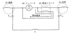
ここで、図4は零相電圧・零相電流に着目したインバータシステムの等価回路図である。
ここでは、インバータ40(ダイオード整流回路を含めて示してある)は零相電圧を発生する電圧源と見なし、電源10及び負荷50は、高周波的にはそれぞれが浮遊容量CS,CLと配線や接地線のインダクタンスLとを介して接地されていると見なしている。なお、一般的にインバータ40の浮遊容量は、例えば三相誘導電動機等の負荷50に比べて小さいこと、及び、電源10や負荷50とインバータ40とを接続する配線インダクタンスは接地線のインダクタンスLに比べて小さいことから、この図ではインバータ40の浮遊容量を省略してある。
この図のような等価回路によれば、インバータ40によって零相電圧が発生すると負荷50から電源10の経路で零相電流が流れることが容易に理解できる。
【0010】
図5は、本発明において同じく零相電圧・零相電流に着目したインバータシステムの等価回路図である。
この図5では、図4に対して、零相電圧の電圧源であるインバータ40と負荷50との間に零相トランス60が接続されており、その二次巻線はインバータ40に並列に接続されている。
この図から明らかなように、零相トランス60の二次側には、零相電圧の電圧源相当の電圧が加わり、零相トランス60の一次側にも同等の電圧が発生する。これにより、負荷50の浮遊容量CLを通る経路では零相電圧がキャンセルされ、負荷50側の零相電流が低減されると共に、回路構成上、電源10側の零相電流も低減されることがわかる。
【0011】
また、図6に示すように、零相トランス60をインバータ40の交流入力側に挿入したり、あるいはインバータ40の直流中間回路に挿入しても動作上は図5と同様になり、同様の効果を得ることができる。このように、零相トランス60は、インバータ40を零相電圧源とする零相電流の経路内であればどの位置に挿入しても良い。
【0012】
【発明の実施の形態】
以下、図に沿って本発明の実施形態を説明する。
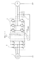
まず、図1は請求項1の発明に相当する第1実施形態を示す回路図である。本実施形態において、装置全体の構成要素は図7と同様である。すなわち、1は交流電圧源としての三相交流電源、2はダイオードD1〜D6からなるダイオード整流回路、3は直流中間回路(正電位点P−負電位点N間)に接続された平滑コンデンサ、4は各々に逆並列ダイオードが接続されたIGBT等の自己消弧形半導体スイッチ素子Tr1〜Tr6からなる三相電圧形インバータ、5は三相誘導電動機等の負荷、6は二次側巻線62を含む4つの巻線が互いに密結合された零相トランス、7はインバータ4の交流出力側に3個のコンデンサが星形結線されたコンデンサ回路であり、その中性点は前記二次側巻線62の一端に接続されている。なお、この図では、三相交流電源1及び負荷5の浮遊容量は図示していない。
【0013】
上記構成から明らかなように、本実施形態では、三相交流電源1の交流電圧をダイオード整流回路2により整流した直流電圧を入力としてインバータ部4により直流−交流電力変換を行い、三相交流電圧を負荷5に供給している。そして、交流出力電圧の相数をn(=3)とすると、インバータ部4の三相交流出力端子を、互いに密結合しているn+1(=4)個の巻線を有する零相トランス6のn(=3)個の巻線を介して負荷5に接続すると共に、前記三相交流出力端子を、n(=3)個のコンデンサが星形結線されたコンデンサ回路7の各コンデンサの一端に接続し、その中性点を零相トランス6の残りの1個の巻線(二次側巻線)を介し直流中間回路の一方の電位点に接続するものである。
なお、図示されていないが、単相電圧形インバータにおいては、インバータ部の交流出力端子数、零相トランスの巻線数及びコンデンサ回路のコンデンサ数等に関し、上記の数nを2とする。
【0014】
さて、図1の実施形態では、零相トランス6の二次側巻線62の他端がインバータ部4の直流中間回路の負電位点Nに接続されている。
このように接続すると、先に示した図5と同様に、零相トランス6の二次側巻線62にはインバータ部4によって零相電圧の電圧源相当の電圧が加わり、零相トランス6の一次側(負荷5の入力側)にも同等の電圧が発生する。これにより、負荷5の浮遊容量を通る経路においては零相電圧がキャンセルされ、負荷5側の零相電流が低減される。これと同時に、二次側巻線62の一端が接地されずに直流中間回路の負電位点Nに接続されているので、配線や接地線のインダクタンスを介して流れる電源1側の零相電流も低減されることになる。
【0015】
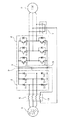
次に、図2は請求項2の発明に相当する第2実施形態を示している。
この実施形態では、直流中間回路の正電位側、負電位側に、3個の巻線が互いに密結合された零相トランス6Aの2個の巻線を挿入し、その二次側巻線62Aの一端を直流中間回路の負電位点Nに接続すると共に、他端をコンデンサ回路7の中性点に接続してある。
なお、単相電圧形インバータの場合にも合計3個の巻線を有する零相トランス6Aを用い、インバータ部の2つの交流出力端子を2個の星形結線されたコンデンサからなるコンデンサ回路に接続してその中性点と直流中間回路の一方の電位点との間に零相トランス62の二次側巻線62Aを接続するものである。
【0016】
本実施形態においても、インバータ部4からなる零相電圧源に対して二次側巻線62Aが並列に接続されており、零相トランス6Aの作用によってインバータ部4から負荷5を通る経路の零相電流が低減され、これによって電源1を通る経路の零相電流も大幅に低減される。
【0017】
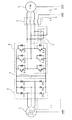
図3は請求項3の発明に相当する第3実施形態であり、原理上、図6の構成に対応している。
本実施形態では、零相トランス6が三相交流電源1とダイオード整流回路2との間に挿入され、その二次側巻線62がコンデンサ回路7の中性点と直流中間回路の負電位点との間に接続されている。
この実施形態においても、インバータ部4からなる零相電圧源に対して二次側巻線62が並列に接続されており、零相トランス6の作用によってインバータ部4から負荷5を通る経路の零相電流が低減される。このため、電源1を通る経路の零相電流も大幅に低減されることになる。
単相電圧形インバータの場合には、図1の実施形態と同様に、インバータ部の交流出力端子数、零相トランスの巻線数及びコンデンサ回路のコンデンサ数等が変更される。
【0018】
なお、上記各実施形態において、零相トランス6または6Aの一次側巻線と二次側巻線との巻数比を変更すれば、二次側巻線62または62Aを通る経路の零相電流を低減させることができる。
また、上記各実施形態では、二次側巻線62または62Aの一端を直流中間回路の負電位点に接続してあるが、正電位点に接続しても良い。
【0019】
【発明の効果】
以上のように請求項1〜3記載の発明によれば、零相トランスをインバータ部の交流出力側、直流中間回路または交流入力側に挿入し、その二次側巻線を零相電圧源としてのインバータ部に対し並列に接続することにより、負荷を流れる零相電流を低減して交流電源側の零相電流を低減することができる。
これにより、周辺機器への悪影響を回避し、また、電源側零相電流に起因する雑音端子電圧の低減も可能になる。
更に、請求項4記載の発明によれば、零相トランスの二次側巻線を通る経路の零相電流を低減させることができる。
【図面の簡単な説明】
【図1】本発明の第1実施形態を示す回路図である。
【図2】本発明の第2実施形態を示す回路図である。
【図3】本発明の第3実施形態を示す回路図である。
【図4】零相電圧・零相電流に着目したインバータシステムの等価回路図である。
【図5】本発明の原理を説明するためのインバータシステムの等価回路図である。
【図6】本発明の原理を説明するためのインバータシステムの等価回路図である。
【図7】従来技術を示す回路図である。
【符号の説明】
1 三相交流電源
2 ダイオード整流回路
3 平滑コンデンサ
4 インバータ部
5 負荷
6,6A 零相トランス
7 コンデンサ回路
10 電源
40 インバータ
50 負荷
60 零相トランス
62,62A 二次側巻線
Tr1〜Tr6 自己消弧形半導体スイッチ素子
D1〜D6 ダイオード[0001]
BACKGROUND OF THE INVENTION
The present invention relates to a voltage source inverter for driving an AC motor or the like at a variable speed, and more particularly to a technique for reducing a zero-phase current of the voltage source inverter.
[0002]
[Prior art]
FIG. 7 shows a conventional technique configured to reduce the leakage current of the three-phase voltage source inverter.
In the figure, 1 is a three-phase AC power source as an AC voltage source, 2 is a diode rectifier circuit composed of diodes D1 to D6, 3 is a smoothing capacitor, and 4 is a self-extinguishing type such as an IGBT to which an antiparallel diode is connected. Inverter unit composed of semiconductor switch elements Tr1 to Tr6, 5 is a load such as a three-phase induction motor, 6 is a zero-phase transformer in which four windings are tightly coupled to each other, 7 is an AC output side of
[0003]
Briefly describing the operation of the circuit shown in FIG. 7, basically, the zero-
[0004]
[Problems to be solved by the invention]
According to the circuit configuration of FIG. 7, i2 which is the zero-phase current between the neutral point on the load side and the ground can be surely reduced, but i1 which is the zero-phase current on the power source side is the sum of i2 and i3. Therefore, it is not reduced unless i3 is reduced.
Therefore, the peripheral device may be adversely affected by i1 which is the zero-phase current on the power supply side. In addition, the noise terminal voltage that serves as a reference for the noise regulation value is determined by the zero-phase current on the power supply side and the current flowing through the stray capacitance between the lines, so this noise terminal voltage is not reduced.
Therefore, the present invention is intended to provide a voltage source inverter that reduces the zero-phase current on the power source side to suppress adverse effects on peripheral devices and enables the reduction of the noise terminal voltage.
[0005]
[Means for Solving the Problems]
In order to solve the above-mentioned problem, the invention described in claim 1 performs DC-AC power conversion by an inverter unit using a DC voltage obtained by rectifying an AC voltage by a rectifier circuit, and performs n-phase (n ≧ 2 and n = 2 is a single phase, and so on.) In a voltage source inverter that outputs an AC voltage to a load, the n-phase AC output terminal of the inverter unit has (n + 1) windings that are tightly coupled to each other. The n-phase AC output terminal is connected to a load via n windings of a zero-phase transformer, and the capacitor circuit is connected to one end of each capacitor of a capacitor circuit in which n capacitors are star-connected. said n winding of the neutral point via the remaining one winding of the zero-phase transformer connected to one potential point of the DC intermediate circuit, and, as a primary winding of the zero-phase transformer Wire and secondary winding as Serial by changing the turns ratio of the remaining one winding is intended to be connected.
[0006]
The invention according to
[0007]
According to a third aspect of the present invention, there is provided a voltage source inverter that performs DC-AC power conversion by an inverter unit using a DC voltage obtained by rectifying an AC voltage by a rectifier circuit and outputs an n-phase AC voltage to a load. Are connected to the rectifier circuit through n windings of a zero-phase transformer having (n + 1) windings that are tightly coupled to each other, and the n-phase AC output terminals are , N capacitors are connected to one end of each capacitor of the star-connected capacitor circuit, and the neutral point of this capacitor circuit is connected to one of the DC intermediate circuits via the remaining one winding of the zero-phase transformer. Are connected to the potential point.
[0008]
According to a fourth aspect of the present invention, in the voltage source inverter according to the second or third aspect, the winding ratio of the primary side winding and the secondary side winding of the zero-phase transformer is changed and connected.
[0009]
Here, FIG. 4 is an equivalent circuit diagram of the inverter system focusing on the zero-phase voltage and the zero-phase current.
Here, the inverter 40 (shown including the diode rectifier circuit) is regarded as a voltage source that generates a zero-phase voltage, and the power source 10 and the load 50 are respectively connected to the stray capacitances C S and C L in terms of high frequency. And grounded via the inductance L of the grounding wire. In general, the stray capacitance of the inverter 40 is smaller than that of the load 50 such as a three-phase induction motor, and the wiring inductance connecting the power source 10 or the load 50 and the inverter 40 is the inductance L of the ground line. In this figure, the stray capacitance of the inverter 40 is omitted because it is small.
According to the equivalent circuit as shown in this figure, it can be easily understood that when a zero-phase voltage is generated by the inverter 40, a zero-phase current flows from the load 50 through the path of the power source 10.
[0010]
FIG. 5 is an equivalent circuit diagram of an inverter system that pays attention to the zero-phase voltage and the zero-phase current in the present invention.
In FIG. 5, a zero-phase transformer 60 is connected between the inverter 40, which is a voltage source of zero-phase voltage, and the load 50, and its secondary winding is connected in parallel to the inverter 40. Has been.
As is apparent from this figure, a voltage equivalent to a voltage source of the zero-phase voltage is applied to the secondary side of the zero-phase transformer 60, and an equivalent voltage is also generated on the primary side of the zero-phase transformer 60. Thus, a path through the stray capacitance C L of the load 50 is canceled zero-phase voltage, with zero-phase current of the load 50 side is reduced, the circuit configuration, the zero-phase current of the power supply 10 side is reduced I understand.
[0011]
Further, as shown in FIG. 6, even if the zero-phase transformer 60 is inserted into the AC input side of the inverter 40 or inserted into the DC intermediate circuit of the inverter 40, the operation is the same as in FIG. Can be obtained. Thus, the zero-phase transformer 60 may be inserted at any position within the path of the zero-phase current using the inverter 40 as the zero-phase voltage source.
[0012]
DETAILED DESCRIPTION OF THE INVENTION
Hereinafter, embodiments of the present invention will be described with reference to the drawings.
FIG. 1 is a circuit diagram showing a first embodiment corresponding to the first aspect of the invention. In this embodiment, the components of the entire apparatus are the same as in FIG. That is, 1 is a three-phase AC power source as an AC voltage source, 2 is a diode rectifier circuit composed of diodes D1 to D6, 3 is a smoothing capacitor connected to a DC intermediate circuit (between positive potential point P and negative potential point N), 4 is a three-phase voltage source inverter composed of self-extinguishing semiconductor switching elements Tr1 to Tr6 such as IGBTs each connected with an antiparallel diode, 5 is a load such as a three-phase induction motor, and 6 is a
[0013]
As is apparent from the above configuration, in the present embodiment, a DC voltage obtained by rectifying the AC voltage of the three-phase AC power source 1 by the
Although not shown, in the single-phase voltage source inverter, the number n is set to 2 with respect to the number of AC output terminals of the inverter unit, the number of windings of the zero-phase transformer, the number of capacitors of the capacitor circuit, and the like.
[0014]
In the embodiment of FIG. 1, the other end of the secondary winding 62 of the zero-
When connected in this way, a voltage corresponding to the voltage source of the zero-phase voltage is applied to the secondary winding 62 of the zero-
[0015]
Next, FIG. 2 shows a second embodiment corresponding to the invention of
In this embodiment, two windings of a zero-phase transformer 6A in which three windings are tightly coupled to each other are inserted on the positive potential side and negative potential side of the DC intermediate circuit, and the secondary winding 62A Is connected to the negative potential point N of the DC intermediate circuit, and the other end is connected to the neutral point of the
In the case of a single-phase voltage source inverter as well, a zero-phase transformer 6A having a total of three windings is used, and the two AC output terminals of the inverter section are connected to a capacitor circuit composed of two star-connected capacitors. The secondary winding 62A of the zero-
[0016]
Also in the present embodiment, the secondary winding 62A is connected in parallel to the zero-phase voltage source composed of the
[0017]
FIG. 3 shows a third embodiment corresponding to the invention of
In the present embodiment, the zero-
Also in this embodiment, the secondary winding 62 is connected in parallel to the zero-phase voltage source composed of the
In the case of a single-phase voltage source inverter, the number of AC output terminals of the inverter unit, the number of windings of the zero-phase transformer, the number of capacitors of the capacitor circuit, and the like are changed as in the embodiment of FIG.
[0018]
In each of the above embodiments, if the turns ratio of the primary side winding and the secondary side winding of the zero
Further, in each of the above embodiments, one end of the secondary winding 62 or 62A is connected to the negative potential point of the DC intermediate circuit, but it may be connected to a positive potential point.
[0019]
【The invention's effect】
As described above, according to the first to third aspects of the present invention, the zero-phase transformer is inserted into the AC output side, the DC intermediate circuit or the AC input side of the inverter unit, and the secondary winding is used as the zero-phase voltage source. By connecting in parallel to the inverter section, the zero-phase current flowing through the load can be reduced and the zero-phase current on the AC power supply side can be reduced.
As a result, adverse effects on the peripheral devices can be avoided, and the noise terminal voltage caused by the power-source side zero-phase current can be reduced.
Furthermore, according to the fourth aspect of the present invention, the zero-phase current in the path passing through the secondary winding of the zero-phase transformer can be reduced.
[Brief description of the drawings]
FIG. 1 is a circuit diagram showing a first embodiment of the present invention.
FIG. 2 is a circuit diagram showing a second embodiment of the present invention.
FIG. 3 is a circuit diagram showing a third embodiment of the present invention.
FIG. 4 is an equivalent circuit diagram of an inverter system focusing on zero-phase voltage and zero-phase current.
FIG. 5 is an equivalent circuit diagram of an inverter system for explaining the principle of the present invention.
FIG. 6 is an equivalent circuit diagram of an inverter system for explaining the principle of the present invention.
FIG. 7 is a circuit diagram showing a conventional technique.
[Explanation of symbols]
DESCRIPTION OF SYMBOLS 1 Three-phase alternating
Claims (4)
前記インバータ部のn相交流出力端子を、互いに密結合している(n+1)個の巻線を有する零相トランスのn個の巻線を介して負荷に接続すると共に、前記n相交流出力端子を、n個のコンデンサが星形結線されたコンデンサ回路の各コンデンサの一端に接続し、このコンデンサ回路の中性点を前記零相トランスの残りの1個の巻線を介して直流中間回路の一方の電位点に接続し、かつ、
前記零相トランスの一次側巻線としての前記n個の巻線と二次側巻線としての前記残りの1個の巻線との巻数比を変更して接続することを特徴とする電圧形インバータ。A voltage that performs DC-AC power conversion by an inverter unit using a DC voltage rectified by a rectifier circuit as an input, and outputs an n-phase (n ≧ 2 and n = 2 is a single phase) AC voltage to a load. In the inverter
The n-phase AC output terminal of the inverter unit is connected to a load via n windings of a zero-phase transformer having (n + 1) windings that are tightly coupled to each other, and the n-phase AC output terminal Is connected to one end of each capacitor of a capacitor circuit in which n capacitors are star-connected, and the neutral point of this capacitor circuit is connected to the DC intermediate circuit via the remaining one winding of the zero-phase transformer. Connected to one potential point , and
A voltage type wherein the n number of windings as the primary side winding of the zero-phase transformer and the remaining one winding as the secondary side winding are changed and connected. Inverter.
直流中間回路の正電位側及び負電位側に、互いに密結合している3個の巻線を有する零相トランスの2個の巻線を介在させると共に、前記n相交流出力端子を、n個のコンデンサが星形結線されたコンデンサ回路の各コンデンサの一端に接続し、このコンデンサ回路の中性点を前記零相トランスの残りの1個の巻線を介して直流中間回路の一方の電位点に接続したことを特徴とする電圧形インバータ。A voltage that performs DC-AC power conversion by an inverter unit using a DC voltage rectified by a rectifier circuit as an input, and outputs an n-phase (n ≧ 2 and n = 2 is a single phase) AC voltage to a load. In the inverter
Two windings of a zero-phase transformer having three windings tightly coupled to each other are interposed on the positive potential side and the negative potential side of the DC intermediate circuit, and n number of the n-phase AC output terminals are provided. Is connected to one end of each capacitor of the star-connected capacitor circuit, and the neutral point of this capacitor circuit is connected to one potential point of the DC intermediate circuit via the remaining one winding of the zero-phase transformer. A voltage-type inverter characterized by being connected to.
前記交流電圧源のn相交流出力端子を、互いに密結合している(n+1)個の巻線を有する零相トランスのn個の巻線を介して前記整流回路に接続すると共に、前記n相交流出力端子を、n個のコンデンサが星形結線されたコンデンサ回路の各コンデンサの一端に接続し、このコンデンサ回路の中性点を、前記零相トランスの残りの1個の巻線を介し直流中間回路の一方の電位点に接続したことを特徴とする電圧形インバータ。A voltage that performs DC-AC power conversion by an inverter unit using a DC voltage rectified by a rectifier circuit as an input, and outputs an n-phase (n ≧ 2 and n = 2 is a single phase) AC voltage to a load. In the inverter
The n-phase AC output terminal of the AC voltage source is connected to the rectifier circuit through n windings of a zero-phase transformer having (n + 1) windings that are tightly coupled to each other, and the n-phase The AC output terminal is connected to one end of each capacitor of a capacitor circuit in which n capacitors are star-connected, and the neutral point of this capacitor circuit is connected to the DC via the remaining one winding of the zero-phase transformer. A voltage source inverter connected to one potential point of an intermediate circuit.
前記零相トランスの一次側巻線と二次側巻線との巻数比を変更して接続することを特徴とする電圧形インバータ。The voltage source inverter according to claim 2 or 3,
A voltage source inverter, wherein the winding ratio of the primary side winding and the secondary side winding of the zero-phase transformer is changed and connected.
Priority Applications (1)
| Application Number | Priority Date | Filing Date | Title |
|---|---|---|---|
| JP27833597A JP3661737B2 (en) | 1997-10-13 | 1997-10-13 | Voltage type inverter |
Applications Claiming Priority (1)
| Application Number | Priority Date | Filing Date | Title |
|---|---|---|---|
| JP27833597A JP3661737B2 (en) | 1997-10-13 | 1997-10-13 | Voltage type inverter |
Publications (2)
| Publication Number | Publication Date |
|---|---|
| JPH11122953A JPH11122953A (en) | 1999-04-30 |
| JP3661737B2 true JP3661737B2 (en) | 2005-06-22 |
Family
ID=17595906
Family Applications (1)
| Application Number | Title | Priority Date | Filing Date |
|---|---|---|---|
| JP27833597A Expired - Fee Related JP3661737B2 (en) | 1997-10-13 | 1997-10-13 | Voltage type inverter |
Country Status (1)
| Country | Link |
|---|---|
| JP (1) | JP3661737B2 (en) |
Families Citing this family (8)
| Publication number | Priority date | Publication date | Assignee | Title |
|---|---|---|---|---|
| JP3393374B2 (en) * | 1999-09-14 | 2003-04-07 | 株式会社日立製作所 | Power conversion system |
| KR100974619B1 (en) | 2003-09-15 | 2010-08-06 | 현대중공업 주식회사 | The suppresses system the overvoltage which is input in the electric motor to the inverter system that use filter design method and this |
| JP2005143230A (en) * | 2003-11-07 | 2005-06-02 | Yaskawa Electric Corp | Filtering device for matrix converter |
| CZ297931B6 (en) * | 2004-11-02 | 2007-05-02 | Azd Praha S. R. O. | Safe three-phase contactless switch |
| JP2007181341A (en) * | 2005-12-28 | 2007-07-12 | Yaskawa Electric Corp | Converter device |
| JP5093452B2 (en) * | 2007-03-07 | 2012-12-12 | 学校法人同志社 | Common mode leakage current suppression circuit applied to power conversion equipment |
| JP5147624B2 (en) * | 2008-09-30 | 2013-02-20 | 株式会社日立製作所 | Inverter device |
| JPWO2010100934A1 (en) * | 2009-03-05 | 2012-09-06 | 三菱電機株式会社 | Leakage current reduction device |
-
1997
- 1997-10-13 JP JP27833597A patent/JP3661737B2/en not_active Expired - Fee Related
Also Published As
| Publication number | Publication date |
|---|---|
| JPH11122953A (en) | 1999-04-30 |
Similar Documents
| Publication | Publication Date | Title |
|---|---|---|
| US6288915B1 (en) | Converter circuit arrangement having a DC intermediate circuit | |
| EP1564875B1 (en) | Filter | |
| US7602622B2 (en) | Compensator with filter for use with a three-phase drive powering a one-phase load | |
| US5952812A (en) | AC-DC power converting device | |
| US7548439B2 (en) | Electric power converter for reducing generated high frequency components | |
| US4519022A (en) | Ripple reduction circuit for an inverter | |
| JP3661737B2 (en) | Voltage type inverter | |
| JP3912096B2 (en) | Noise reduction device for power converter | |
| JP2004222421A (en) | Power conversion apparatus | |
| WO2017183426A1 (en) | Motor driving device | |
| JP3063354B2 (en) | General-purpose inverter | |
| JP3656705B2 (en) | Voltage type inverter | |
| US20090016089A1 (en) | Electromechanical power transfer system with even phase number dynamoelectric machine and three level inverter | |
| JPH08237936A (en) | Noise filter for voltage type inverter | |
| JPH07123350B2 (en) | Inverter device | |
| JP2004007991A (en) | Drive unit of electric vehicle | |
| JP2000308368A (en) | Power conversion circuit | |
| JP3535321B2 (en) | Electric vehicle drive | |
| JPH09103078A (en) | Power converter | |
| JP2002044953A (en) | Rectifier of three-phase half-voltage output type | |
| JPH0746847A (en) | Three-phase rectifier | |
| JP3316858B2 (en) | Constant voltage / constant frequency power supply | |
| JP3246584B2 (en) | AC / DC converter | |
| JP2004056882A (en) | Multilevel pwm inverter controller | |
| JP6636219B1 (en) | Power converter |
Legal Events
| Date | Code | Title | Description |
|---|---|---|---|
| RD04 | Notification of resignation of power of attorney |
Free format text: JAPANESE INTERMEDIATE CODE: A7424 Effective date: 20040205 |
|
| A977 | Report on retrieval |
Free format text: JAPANESE INTERMEDIATE CODE: A971007 Effective date: 20041201 |
|
| A131 | Notification of reasons for refusal |
Free format text: JAPANESE INTERMEDIATE CODE: A131 Effective date: 20041209 |
|
| A521 | Written amendment |
Free format text: JAPANESE INTERMEDIATE CODE: A523 Effective date: 20050204 |
|
| TRDD | Decision of grant or rejection written | ||
| A01 | Written decision to grant a patent or to grant a registration (utility model) |
Free format text: JAPANESE INTERMEDIATE CODE: A01 Effective date: 20050302 |
|
| A61 | First payment of annual fees (during grant procedure) |
Free format text: JAPANESE INTERMEDIATE CODE: A61 Effective date: 20050315 |
|
| R150 | Certificate of patent or registration of utility model |
Free format text: JAPANESE INTERMEDIATE CODE: R150 |
|
| FPAY | Renewal fee payment (event date is renewal date of database) |
Free format text: PAYMENT UNTIL: 20080401 Year of fee payment: 3 |
|
| FPAY | Renewal fee payment (event date is renewal date of database) |
Free format text: PAYMENT UNTIL: 20090401 Year of fee payment: 4 |
|
| FPAY | Renewal fee payment (event date is renewal date of database) |
Free format text: PAYMENT UNTIL: 20090401 Year of fee payment: 4 |
|
| S111 | Request for change of ownership or part of ownership |
Free format text: JAPANESE INTERMEDIATE CODE: R313111 |
|
| FPAY | Renewal fee payment (event date is renewal date of database) |
Free format text: PAYMENT UNTIL: 20090401 Year of fee payment: 4 |
|
| R350 | Written notification of registration of transfer |
Free format text: JAPANESE INTERMEDIATE CODE: R350 |
|
| FPAY | Renewal fee payment (event date is renewal date of database) |
Free format text: PAYMENT UNTIL: 20100401 Year of fee payment: 5 |
|
| FPAY | Renewal fee payment (event date is renewal date of database) |
Free format text: PAYMENT UNTIL: 20110401 Year of fee payment: 6 |
|
| FPAY | Renewal fee payment (event date is renewal date of database) |
Free format text: PAYMENT UNTIL: 20120401 Year of fee payment: 7 |
|
| S111 | Request for change of ownership or part of ownership |
Free format text: JAPANESE INTERMEDIATE CODE: R313111 |
|
| FPAY | Renewal fee payment (event date is renewal date of database) |
Free format text: PAYMENT UNTIL: 20120401 Year of fee payment: 7 |
|
| R350 | Written notification of registration of transfer |
Free format text: JAPANESE INTERMEDIATE CODE: R350 |
|
| FPAY | Renewal fee payment (event date is renewal date of database) |
Free format text: PAYMENT UNTIL: 20120401 Year of fee payment: 7 |
|
| FPAY | Renewal fee payment (event date is renewal date of database) |
Free format text: PAYMENT UNTIL: 20130401 Year of fee payment: 8 |
|
| FPAY | Renewal fee payment (event date is renewal date of database) |
Free format text: PAYMENT UNTIL: 20130401 Year of fee payment: 8 |
|
| FPAY | Renewal fee payment (event date is renewal date of database) |
Free format text: PAYMENT UNTIL: 20140401 Year of fee payment: 9 |
|
| LAPS | Cancellation because of no payment of annual fees |