JP3631462B2 - Method and apparatus for measuring full frame size based on display signal - Google Patents
Method and apparatus for measuring full frame size based on display signal Download PDFInfo
- Publication number
- JP3631462B2 JP3631462B2 JP2001380543A JP2001380543A JP3631462B2 JP 3631462 B2 JP3631462 B2 JP 3631462B2 JP 2001380543 A JP2001380543 A JP 2001380543A JP 2001380543 A JP2001380543 A JP 2001380543A JP 3631462 B2 JP3631462 B2 JP 3631462B2
- Authority
- JP
- Japan
- Prior art keywords
- signal
- display
- primary color
- data enable
- full frame
- Prior art date
- Legal status (The legal status is an assumption and is not a legal conclusion. Google has not performed a legal analysis and makes no representation as to the accuracy of the status listed.)
- Expired - Fee Related
Links
Images


Classifications
-
- G—PHYSICS
- G06—COMPUTING; CALCULATING OR COUNTING
- G06F—ELECTRIC DIGITAL DATA PROCESSING
- G06F3/00—Input arrangements for transferring data to be processed into a form capable of being handled by the computer; Output arrangements for transferring data from processing unit to output unit, e.g. interface arrangements
- G06F3/14—Digital output to display device ; Cooperation and interconnection of the display device with other functional units
- G06F3/147—Digital output to display device ; Cooperation and interconnection of the display device with other functional units using display panels
-
- G—PHYSICS
- G06—COMPUTING; CALCULATING OR COUNTING
- G06F—ELECTRIC DIGITAL DATA PROCESSING
- G06F3/00—Input arrangements for transferring data to be processed into a form capable of being handled by the computer; Output arrangements for transferring data from processing unit to output unit, e.g. interface arrangements
- G06F3/14—Digital output to display device ; Cooperation and interconnection of the display device with other functional units
- G06F3/153—Digital output to display device ; Cooperation and interconnection of the display device with other functional units using cathode-ray tubes
-
- G—PHYSICS
- G09—EDUCATION; CRYPTOGRAPHY; DISPLAY; ADVERTISING; SEALS
- G09G—ARRANGEMENTS OR CIRCUITS FOR CONTROL OF INDICATING DEVICES USING STATIC MEANS TO PRESENT VARIABLE INFORMATION
- G09G2340/00—Aspects of display data processing
- G09G2340/04—Changes in size, position or resolution of an image
- G09G2340/0407—Resolution change, inclusive of the use of different resolutions for different screen areas
-
- G—PHYSICS
- G09—EDUCATION; CRYPTOGRAPHY; DISPLAY; ADVERTISING; SEALS
- G09G—ARRANGEMENTS OR CIRCUITS FOR CONTROL OF INDICATING DEVICES USING STATIC MEANS TO PRESENT VARIABLE INFORMATION
- G09G2340/00—Aspects of display data processing
- G09G2340/04—Changes in size, position or resolution of an image
- G09G2340/0464—Positioning
Description
【0001】
【発明の属する技術分野】
この出願は、2001年1月5日に出願された台湾出願第090100317号を参照として含む。
この発明は、概して、表示信号に基づいてフルフレームサイズを測定するための方法およびその装置に関し、さらに詳細にはデータ・イネーブル信号による表示信号に基づいてフルフレームサイズを測定するための方法およびその装置に関する。
【0002】
【関連技術の説明】
表示特性を維持するために、ブラウン管(CRT)や液晶表示(LCD)モニターなどの表示モニターは、その表示モニターに印加された表示信号により指示されたフルフレームのサイズや位置を調整する必要がある。表示信号により指示された表示フレームを、表示モニターのスクリーン上の適切な位置に表示するために、表示モニターは、フルフレームサイズのような表示パラメータを決定しなければならない。従来の方法および装置が有する問題点を説明するために、次に表示モニターの電気回路構成、表示信号、およびフルフレームのサイズと位置の決定について説明する。
【0003】
表示モニターの電気回路構成が、図1に示されている。表示モニターは、差分信号受信/復号装置110と比処理装置とを含む。表示モニターに付加された表示信号は、一般に、低電圧差分(LVD)符号化信号である。LVD符号化信号とは、三原色信号、水平同期信号Hs、垂直同期信号Vs、データ・イネーブル信号DE、および画素クロック信号CKを含む信号を指す。図1において、LVD符号化信号102は、Rx0−、Rx0+、Rx1−、Rx1+、Rx2−、Rx2+、RxC−、およびRxC+により示された信号を含む。表示モニターはこれらの信号を処理する前にはデジタル信号だけしか表示できないので、表示モニターは、これらの信号をデジタル表示信号104に変換および復号するために、差分信号受信/復号装置110を使用する。LVD符号化信号102を受信すると、差分信号受信/復号装置110は、このLVD符号化信号102をデジタル表示信号104(すなわち赤色(RD)、緑色(GD)、青色信号(BD)を含む三原色信号)、水平同期信号Hs、垂直同期信号Vs、データ・イネーブル信号DE、および画素クロックCK等に変換および復号する。デジタル表示信号104が比処理装置130に印加されると、比処理装置130が位相調整または補間を行なうことにより、適切な出力ビデオ信号が得られる。位相調整または補間は、フルフレームサイズ測定の中心ではないので、それらについての説明は省略する。水平同期信号Hs、垂直同期信号Vs、データ・イネーブル信号DE、および画素クロック信号CKを印加された表示モニターの作動については後述する。
【0004】
水平同期信号Hs、垂直同期信号Vs、データ・イネーブル信号DE、および画素クロック信号CKは、複数ユニットの周波数を有する。画素クロック信号CKは、1秒当りに表示される画素数を示し、カラー表示する1個の画素とカラー表示する次の画素との間の間隔を決定する。フレームのデータを受信すると、表示モニターはフレームの画素の色を1本ずつ線で表示する。まず、最初の線の最初の画素が色を表示する。次に、最初の線の2番目の画素が色を表示する。このプロセスは、最初の線の最後の画素が色を表示するまで、同様に続けられる。その後に、次の線、たとえば2番目の線が同様に最初の画素から最後の画素まで色を表示する。同様に、最後の線の最後の画素が色を表示するまで、このプロセスが続く。人間の視覚システムは視覚の持続性を有しているため、スクリーン上のすべての画素は、必要とされるフレームを形成する。他のフレームを受け取ると、表示モニターは同じ方法でフレームを表示する。各線の最後の画素が色を表示した後、水平同期信号Hsは、カラー表示する画素の走査を次の線の最初の画素から進めることが重要である。そのようにして、水平同期信号Hsは、1秒間に色を表示する画素の横列数を決定する。さらに、最終縦列最終横列の画素が色を表示した後、垂直同期信号Vsは、カラー表示する画素の走査を第1縦列第1横列の画素から進める。そのようにして、垂直同期信号Vsは、1秒当りに表示されるフレームの数を決定する。人間の視覚システムは視覚の持続性を有しているため、閾値よりも速い速度で表示されたフレームは、たとえば映画のように対象の連続運動となる。表示モニターが異なるフレームを更新(リフレッシュ)する速度をリフレッシュレートと呼び、これは垂直同期信号Vsの周波数である。一般的なコンピュータ表示システムのリフレッシュレートは60Hz以上であり、すなわち表示モニターは1秒当り少なくとも60フレームを表示する。下記において、水平同期信号Hs、垂直同期信号Vs、データ・イネーブル信号DE、および画素クロック信号CKのタイミング関係を説明する。
【0005】
図2では、水平同期信号Hs、垂直同期信号Vsおよびデータ・イネーブル信号DEのタイミング関係を説明する。例として1024x768画素の解像度を取り上げる。この解像度のために、水平同期信号Hs、垂直同期信号Vs、および画素クロック信号CKはそれぞれ48.36kHz、60Hz、および65MHzであってよい。フレームの表示期間中、毎秒60個のフレームが表示され、各フレームに768個の横列が存在するため、Vs信号はHs信号の768サイクルの後にのみその状態を変更する。さらに、データ・イネーブル信号DEは各横列の表示期間を決定する。各横列に対し、1024個の画素が表示されるべきである。したがって、データ・イネーブル信号DEが有効になると、表示モニターは1024画素の色を表示する。画素クロック信号CKは固定周波数を有しているため、図2Bに示したように、画素クロック信号CKはそれに対応して、データ・イネーブル信号DEの有効期間中に1024サイクル振動する。次にデジタル表示信号を画素クロック信号CKを介してサンプリングすることにより、1024画素の色情報が得られ、サンプリングされた色情報はデータ・イネーブル信号DEの有効期間中、1024画素に適用される。その結果、データ・イネーブル信号DEはフルフレームサイズの幅を決定するのに利用できる。
【0006】
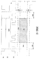
図3は、さらに、表示領域が上記の信号にどのように関連するかを示している。図3に示された表示領域300は、1024x768画素のアレイを示している。表示領域300における各画素の色は、デジタル表示信号を画素クロック信号CKを介してサンプリングすることにより表示されるので、各横列の全ての画素は画素クロック信号CKのパルス列の1024パルスに対応する。図3に示されているように、表示領域300の各横列の長さは、データ・イネーブル信号DEが有効であるときデータ・イネーブル信号DEにより決定される。水平同期信号Hsは表示領域300の各横列の表示を決定するが、各横列の長さはHs信号によっては決定されない。さらに、Hs信号が有効化される各期間の開始後および終了前に、Hs信号が表示領域300に対応しない期間(すなわちHs信号が表示信号300の外側の画素がない領域と対応する期間)が存在し、これらの期間はそれぞれ一般にバックポーチおよびフロントポーチと呼ばれる。たとえば、表示領域300の左側の点線で囲われた四角形は、Hs信号のバックポーチBPHに対応する。表示領域300の右側の点線で囲われた四角形は、Hs信号のフロントポーチFPHに対応する。さらに、垂直同期信号Vsもまた同様にフロントポーチおよびバックポーチを有する。表示領域300の上側の点線で囲われた領域は、Vs信号が表示領域300と対応しない期間に対応し、Vs信号のバックポーチBPVと呼ばれる。表示領域300の下側の点線で囲われた領域は、Vs信号の他の期間に対応し、Vs信号のフロントポーチFPVと呼ばれる。「ポーチ」という言葉が、同期(HsまたはVs)信号が表示領域の外側の表示される画素がない領域に対応する期間を指示するものとして一般に使用されることが、さらに重要である。
【0007】
表示信号により指示されたフレームをスクリーン上の適切な位置に表示するために、従来の表示モニターは、一般に、表示モニターに印加された表示信号によって指示されたフルフレームのサイズおよび位置を、表示信号と表示モニター内に設けられた表示信号設定とを比較して調整する。具体的にいえば、HsおよびVs信号の周波数および極性が、表示モニターに設けられた表示信号設定と比較される。もし表示信号の水平同期信号Hsの周波数および極性が表示モニターに設けられた表示信号設定の1つと一致すると、表示モニターは、決定された表示信号設定用のフレーム調整データを用いて表示信号により指示されたフレームを調整し、それによってフレームを適切な位置に表示する。しかしながら、種々のビデオアダプタが市販されているため、もしビデオアダプタからの表示信号の周波数および極性が表示モニターに設けられた表示信号設定の1つと一致しても、表示信号のフロントポーチおよびバックポーチのためのタイミングが前記の一致した表示信号設定値のタイミングと異なる場合がある。この場合には、もし一致した表示信号設定値のためのフレーム調整データがフレーム調整に用いられると、不適切な調整が行なわれ、フレームをスクリーンの適切な位置に表示できず、その結果表示特性を低下させる。たとえば、フレームが領域からずれて表示されたり、画素の総数が正しくなかったりする。
【0008】
上記の問題を解決するために、表示信号のフロントポーチおよびバックポーチのタイミングを正確に決定するための制御チップが開発されている。しかしながら、これらの制御チップは表示信号により指示されたフレームの最初および最後の画素に基づいてフロントポーチおよびバックポーチを決定する方法を用いており、この場合、フレームの最初および最後の画素は、黒以外の色を表示する。ノンフルサイズフレームまたは黒色を表示するフレームが制御チップに適用されると、フロントポーチおよびバックポーチのタイミングの決定は、予期しない結果をもたらすことがあり、その場合、黒色を表示するフレームは、コマンドモードの黒色スクリーンのように、赤色、緑色および青色を有していない。
【0009】
【発明の概要】
従って、この発明の目的は、デジタル表示信号に基づいてフルフレームサイズを測定するための方法とそのための装置を提供することである。たとえ表示されるべき表示フレームが黒色フレームまたはノンフルフレームであっても、デジタル表示信号により指示された表示フレームのパターンに関係なく、フルフレームサイズを正確に測定することができる。
【0010】
この発明は、データ・イネーブル信号によるデジタル表示信号に基づいてフルフレームサイズを測定する装置を提供することにより、上記の目的を達成する。この場合、デジタル表示信号は多数の表示ビットを有する原色信号を含む。この装置は、タイミング制御装置とマルチプレクシング装置とを含む。タイミング制御装置は、多数の入力端子と1個の制御信号出力端子とを有する。各入力端子は、原色信号の表示ビットに連結できる。タイミング制御装置は制御信号出力端子を介して制御信号を出力する。さらに、制御信号は表示調整を行なうべきかどうかを指示するために使用される。マルチプレクシング装置は、タイミング制御装置とデータ・イネーブル信号と原色信号のn番目のビットに連結されている。マルチプレクシング装置は、制御信号に基づいて、データ・イネーブル信号と原色信号のn番目のビットとのいずれかを選択してタイミング制御装置のn番目の入力端子に付加する。この場合、nはmよりも大きくなく、nとmは0よりも大きい整数である。
【0011】
デジタル表示信号の実際のフレームを表示しなければならないとき、原色カラー表示ビットのn番目のビットが選択され、マルチプレクシング装置を介してタイミング制御装置に付加される。タイミング制御装置が表示調整を行なわねばならないとき、タイミング制御装置はデータ・イネーブル信号をマルチプレクシング装置に出力し、マルチプレクシング装置はそのデータ・イネーブル信号をタイミング制御装置に付加する。データ・イネーブル信号に基づいて、タイミング制御装置は、フルフレームのサイズおよび位置が得られるように、フロントポーチおよびバックポーチのような表示パラメータを決定する。表示調整の後、タイミング制御装置はデータ・イネーブル信号のロジック状態を変更して、タイミング制御装置の入力端子が元来の表示ビット配列を有する原色信号を受け取れるようにし、それによって表示調整に基づいて表示信号が指示したフレームが表示できる。
【0012】
この発明によれば、データ・イネーブル信号による表示信号に基づいてフルフレームサイズを測定する方法が提供され、この場合、表示信号はm個の表示ビットを有する原色信号を含む。この方法は、つぎのステップを含む。最初に、データ・イネーブル信号が提供される。次に、このデータ・イネーブル信号を原色信号のn番目のビットの代わりに用いることにより、代用表示信号が提供される。最後に、データ・イネーブル信号に基づいてフルフレームサイズが測定される。この場合、nはmより大きくなく、mおよびnは0より大きい整数である。
【0013】
上記のように、データ・イネーブル信号は原色信号の1個の表示ビットの代わりに用いられる。この発明によれば、表示パラメータを測定するために、データ・イネーブル信号を異なる方法で他の1個の表示ビットまたは多数の表示ビットの代わりに用いることができる。たとえば、データ・イネーブル信号を、前記原色信号の他の表示ビットまたは多数の表示ビットの代わりに用いることができ、また、タイミング制御装置に付加された他の原色信号の1個または多数の表示ビットの代わりに用いることができる。
【0014】
この発明の他の目的、特徴および利点は、下記の好ましい実施形態から明らかになるであろう。ただし、これらの実施形態は、この発明を限定するものではない。説明は、添付図面を参照して行なう。
【0015】
【発明の実施の形態】
この発明により表示信号に基づいてディスプレイフレームのサイズを測定するために、データ・イネーブル信号をデジタル表示信号の1個または多数の表示ビットの代わりに用い、この表示ビットの代用の後、このデジタル表示信号をディスプレイフレームのサイズを測定するためのタイミング制御装置に送る。データ・イネーブル信号は、表示されるべきフレームを指示するために水平同期信号が有効にされている期間にのみ有効にされるので、表示信号により指示されたフレームが全ブラックフレームまたはノンフルフレームに対応しても、表示ビットの代用の後、フルフレームサイズはディスプレイフレーム位置や解像度のような対応する表示パラメータとともに正確に測定できる。フルフレームサイズの測定により、表示信号のための表示調整を実施できる。フルフレームサイズの測定はいつでも実施できるが、表示ビットの代わりに用いたデジタル表示信号は、表示されるべき実際のイメージに対応しないということに留意すべきである。したがって、フルフレームサイズの測定によって表示の質が影響を受けないようにするために、表示ビット代用後の表示信号を、フルフレームサイズ測定およびディスプレイ調整を実施した後に、元の表示ビット配列に戻すべきである。したがって、実際には、ディスプレイ調整の前と後とに表示ビット代用と表示信号の回復とをそれぞれ行なうために、マルチプレクシング装置を用いて信号を切り換えることができる。
【0016】
図4Aは、この発明の好ましい実施形態によるフルフレームサイズ測定装置を示している。この装置は、マルチプレクシング装置410と、タイミング制御装置430とを含む。タイミング制御装置430は、入力ポートRi、Gi、Biと制御信号端子CTとを含む。入力ポートRi、Gi、Biは、それぞれ三原色信号、すなわち赤色信号RD、緑色信号GD、青色信号BDを受け取るために使用される。三原色信号がタイミング制御装置430に付加されると、タイミング制御装置430はフルフレームサイズ、ディスプレイフレーム位置、それらの信号用の前後ポーチのような表示のためのパラメータを決定できる。タイミング制御装置430は、ピクセルワークス(Pixelworks)社製のPW164−20Rのようなタイミング制御チップであってよい。もし各原色信号をm個の表示ビットで表わすと、それに対応してタイミング制御装置430の各入力ポートにm個の入力端子を設ける必要があることに留意すべきである。例として24ビットの表示信号を取り上げる。この信号の各原色信号、すなわち赤色信号RD、緑色信号GD、青色信号BDは、それぞれ8表示ビットの原色データを有しているため、入力ポートRi、Gi、Biは、対応する原色信号の8表示ビットに合わせた8個の入力端子を有している。表示ビットと入力端子との関係は、後に詳述する。さらに、表示信号の表示ビットの代わりにデータ・イネーブル信号を用いて、表示調整が終わった後に元の表示ビット配列を回復するために、マルチプレクシング装置410はタイミング制御装置430に連結されており、2つの信号、すなわちデータ・イネーブル信号と、このデータ・イネーブル信号が代用する表示信号のいくつかの表示ビットとの切り換えに使用される。この実施形態のデータ・イネーブル信号DEと赤色信号の表示ビットとの切り換えを、図によって説明する。
【0017】
図4Bは図4Aの装置の構造を図示しており、表示ビットと入力端子との関係が詳細に示されている。赤色信号RDは、8個の表示ビット、すなわちRD0、RD1、……、RD7 からなる。同様に、緑色信号GDは、8個の表示ビット、すなわちGD0、GD1、……、GDからなり、青色信号BDは、8個の表示ビット、すなわちBD0、BD2、……、BD7からなる。図4Bにおいて、各表示ビットは、対応する入力ポートの入力端子に連結されている。たとえば、表示ビットRD6は入力ポートRiの入力端子Ri6に連結されており、表示ビットGD7は入力ポートGiの入力端子Gi7に連結されている。図4Bに示した信号および入力端子に関して、データ・イネーブル信号DEは、フルフレームサイズを測定するために、赤色信号RDの最も高い表示ビットRD7の代わりに用いられる。実際には、データ・イネーブル信号DEは、表示パラメータを測定するために別の方法でほかの一個または多数の表示ビットの代わりに用いることができる。たとえば、データ・イネーブル信号DEは、赤色信号RDの他の表示ビットや、赤色信号RDの多数の表示ビットや、他の原色信号の一個または多数の表示ビットの代わりに用いることができる。これらの例は、図4Bに示した実施形態に基づいて容易に得ることができるので、簡潔にするためにこれ以上の説明を省略する。
【0018】
フルフレームサイズを測定するために、データ・イネーブル信号DEと赤色信号の表示ビットとの切り換えが行なわれる。図4Bにおいて、表示信号がタイミング制御装置430に送られると、タイミング制御装置430は制御信号端子CTを介して制御信号Ctrlを出力する。制御信号Ctrlは次にマルチプレクシング装置410のマルチプレクサ415に送られる。制御信号Ctrlの論理状態、たとえば論理1状態に応答して、マルチプレクサ415は、選択的にスイッチSW1を閉じて(入れて)スイッチSW2を開き(切り)、その結果、データ・イネーブル信号DEは赤色信号RDの8番目の表示ビットすなわち表示ビットRD7の代わりに用いられ、入力端子Ri7に送られる。その後、タイミング制御装置430は、フルフレームサイズや位置など測定するために、その計算機能を用いて前後ポーチのような表示パラメータの測定を開始する。このようにして、測定されたフルフレームサイズや位置により、タイミング制御装置430に連結された表示モジュール(図示せず)は、正確に表示信号に基づいてフレームを表示できる。データ・イネーブル信号DEが入力端子Ri7に付加されると、たとえ表示信号が完全なブラックフレームまたはノンフルフレームを示していても、その表示信号により示された表示フレームのパターンにかかわりなく、フルフレームサイズが確定できることに留意すべきである。
【0019】
表示調整の後、タイミング制御装置430は制御信号Ctrlの論理状態を、たとえば論理1から論理0へ変えることができる。マルチプレクシング装置415は、次に、スイッチSW1を開いて(切って)スイッチSW2を閉じ(入れ)、その結果、赤色信号RDの8番目の表示ビットすなわちRD7が入力端子Ri7に入力される。このようにして、タイミング制御装置430は、表示信号の実際の表示ビットを受け取る。さらに、タイミング制御装置430は表示幾何学に基づいて調整を行なうので、表示信号によって示される像は、最適のサイズで最適位置に示される。このようにして最適な表示効果が得られる。
【0020】
さらに、水平同期信号、垂直同期信号または極性信号のように、タイミング制御装置430への入力に変化が起こった場合、タイミング制御装置430は最適な表示特性を維持するために上記の表示パラメータの測定と表示調整を行なうことができる。
フルフレームサイズを測定するために、データ・イネーブル信号DEは、1つの原色信号の最も高い表示ビット、たとえば表示ビットRD7、GD7またはBD7の代わりに用いられるのが好ましいことに留意すべきである。なぜならば、通常、最も高い表示ビットは、たとえば24ビットまたは18ビットカラー解像度のように異なるカラー解像度に用いられるビット数に関係なく使用されるが、低い方の表示ビットは、カラー解像度によっては放棄される場合があるからである。もしデータ・イネーブル信号DEが最も高い表示ビットではない表示ビットの代わりに用いられると、表示信号が低いカラー解像度に用いられるにつれて、その表示ビットは使用されなくなる場合がある。したがって、ディスプレイが種々のカラー解像度をサポートできるように、データ・イネーブル信号DEと最も高い表示ビットとを組み合わせるのが望ましい。上記の実施形態はカラー表示について説明したが、この発明は、発明の精神から逸脱することなくモノクローム表示にも適用できる。
【0021】
上記のように、データ・イネーブル信号を介してフルフレームサイズを測定する方法および装置は、たとえ表示信号により指示されるイメージが全ブラックフレームまたはノンフルフレームに対応する場合であっても、この表示信号に基づいて正確にフルフレームサイズを測定することができ、したがって最適な表示特性を得ることができる。
好ましい実施形態によって例示しながら発明を説明してきたが、本発明がこれに限定されるものではないと解されるべきである。種々の変形ならびに類似の構成および手法を包含することが意図されているのであって、請求項は、これらの変形ならびに類似の構成および手法を包含するように最広義に解釈すべきである。
【図面の簡単な説明】
【図1】従来の表示における低電圧差分信号の処理を示すブロック線図である。
【図2A】図1の差分信号受信/復元装置からの水平同期信号、垂直同期信号およびデータ・イネーブル信号の関係を示すタイミング線図である。
【図2B】図2Aのデータ・イネーブル信号と画素クロック信号との関係を示すタイミング線図である。
【図3】表示領域と種々の信号との関係を示す。
【図4A】この発明の好ましい実施形態によるフルフレームサイズを測定するための装置のブロック線図である。
【図4B】図4Aに示した装置の構造を示す。[0001]
BACKGROUND OF THE INVENTION
This application includes by reference Taiwan application 090100317 filed on January 5, 2001.
The present invention relates generally to a method and apparatus for measuring a full frame size based on a display signal, and more particularly, to a method and a method for measuring a full frame size based on a display signal with a data enable signal. Relates to the device.
[0002]
[Description of related technology]
In order to maintain display characteristics, a display monitor such as a cathode ray tube (CRT) or a liquid crystal display (LCD) monitor needs to adjust the size and position of a full frame indicated by a display signal applied to the display monitor. . In order to display the display frame indicated by the display signal at an appropriate position on the screen of the display monitor, the display monitor must determine display parameters such as the full frame size. In order to explain the problems of the conventional method and apparatus, the determination of the electrical circuit configuration of the display monitor, the display signal, and the size and position of the full frame will now be described.
[0003]
The electric circuit configuration of the display monitor is shown in FIG. The display monitor includes a differential signal receiving /
[0004]
The horizontal synchronization signal Hs, the vertical synchronization signal Vs, the data enable signal DE, and the pixel clock signal CK have a frequency of a plurality of units. The pixel clock signal CK indicates the number of pixels displayed per second, and determines the interval between one pixel for color display and the next pixel for color display. When the frame data is received, the display monitor displays the color of the pixel of the frame one line at a time. First, the first pixel of the first line displays the color. Next, the second pixel of the first line displays the color. This process continues in the same manner until the last pixel of the first line displays color. Thereafter, the next line, for example the second line, similarly displays the color from the first pixel to the last pixel. Similarly, this process continues until the last pixel of the last line displays color. Since the human visual system has visual persistence, every pixel on the screen forms the required frame. When another frame is received, the display monitor displays the frame in the same way. After the last pixel of each line displays a color, the horizontal synchronization signal Hs is important to advance the scanning of the pixel for color display from the first pixel of the next line. As such, the horizontal synchronization signal Hs determines the number of rows of pixels that display color per second. Further, after the pixels in the last column and the last row display colors, the vertical synchronization signal Vs advances scanning of the pixels to be displayed in color from the pixels in the first column and the first row. As such, the vertical synchronization signal Vs determines the number of frames displayed per second. Since the human visual system has visual persistence, a frame displayed at a speed faster than the threshold is a continuous motion of the object, for example, like a movie. The speed at which the display monitor updates (refreshes) different frames is called the refresh rate, which is the frequency of the vertical synchronization signal Vs. A typical computer display system has a refresh rate of 60 Hz or higher, i.e., the display monitor displays at least 60 frames per second. In the following, the timing relationship among the horizontal synchronizing signal Hs, the vertical synchronizing signal Vs, the data enable signal DE, and the pixel clock signal CK will be described.
[0005]
In FIG. 2, the timing relationship among the horizontal synchronizing signal Hs, the vertical synchronizing signal Vs, and the data enable signal DE will be described. Take a resolution of 1024 × 768 pixels as an example. For this resolution, the horizontal synchronization signal Hs, the vertical synchronization signal Vs, and the pixel clock signal CK may be 48.36 kHz, 60 Hz, and 65 MHz, respectively. During the frame display period, 60 frames are displayed per second and there are 768 rows in each frame, so the Vs signal changes its state only after 768 cycles of the Hs signal. Furthermore, the data enable signal DE determines the display period of each row. For each row, 1024 pixels should be displayed. Therefore, when the data enable signal DE becomes valid, the display monitor displays a color of 1024 pixels. Since the pixel clock signal CK has a fixed frequency, as shown in FIG. 2B, the pixel clock signal CK oscillates correspondingly for 1024 cycles during the valid period of the data enable signal DE. Next, the digital display signal is sampled via the pixel clock signal CK to obtain color information of 1024 pixels, and the sampled color information is applied to the 1024 pixels during the effective period of the data enable signal DE. As a result, the data enable signal DE can be used to determine the width of the full frame size.
[0006]
FIG. 3 further shows how the display area relates to the above signals. The
[0007]
In order to display the frame indicated by the display signal at an appropriate position on the screen, a conventional display monitor generally displays the size and position of the full frame indicated by the display signal applied to the display monitor. And the display signal setting provided in the display monitor are compared and adjusted. Specifically, the frequency and polarity of the Hs and Vs signals are compared with the display signal settings provided on the display monitor. If the frequency and polarity of the horizontal synchronizing signal Hs of the display signal coincide with one of the display signal settings provided in the display monitor, the display monitor indicates by the display signal using the frame adjustment data for the determined display signal setting. Adjust the displayed frame, thereby displaying the frame in the appropriate position. However, since various video adapters are commercially available, even if the frequency and polarity of the display signal from the video adapter matches one of the display signal settings provided on the display monitor, the front and back porch of the display signal There is a case where the timing for the above is different from the timing of the matched display signal set value. In this case, if the frame adjustment data for the matching display signal setting value is used for frame adjustment, improper adjustment is performed and the frame cannot be displayed at the appropriate position on the screen, resulting in display characteristics. Reduce. For example, the frame may be displayed off the area, or the total number of pixels may be incorrect.
[0008]
In order to solve the above problems, a control chip for accurately determining the timing of the front porch and the back porch of the display signal has been developed. However, these control chips use a method of determining the front and back porches based on the first and last pixels of the frame indicated by the display signal, where the first and last pixels of the frame are black. Display a color other than. When a non-full size frame or a frame that displays black is applied to the control chip, the determination of the front and back porch timings can have unexpected results, in which case the frame that displays black is It does not have red, green and blue like the mode black screen.
[0009]
SUMMARY OF THE INVENTION
Accordingly, it is an object of the present invention to provide a method and apparatus for measuring full frame size based on a digital display signal. Even if the display frame to be displayed is a black frame or a non-full frame, the full frame size can be accurately measured regardless of the pattern of the display frame indicated by the digital display signal.
[0010]
The present invention achieves the above object by providing an apparatus for measuring a full frame size based on a digital display signal by a data enable signal. In this case, the digital display signal includes a primary color signal having a number of display bits. The apparatus includes a timing control device and a multiplexing device. The timing control device has a large number of input terminals and one control signal output terminal. Each input terminal can be connected to a display bit of a primary color signal. The timing control device outputs a control signal via a control signal output terminal. In addition, the control signal is used to indicate whether display adjustment should be performed. The multiplexing device is connected to the timing control device, the data enable signal, and the nth bit of the primary color signal. Based on the control signal, the multiplexing device selects either the data enable signal or the nth bit of the primary color signal and adds it to the nth input terminal of the timing control device. In this case, n is not larger than m, and n and m are integers larger than 0.
[0011]
When the actual frame of the digital display signal must be displayed, the nth bit of the primary color display bit is selected and added to the timing controller via the multiplexing unit. When the timing controller must make display adjustments, the timing controller outputs a data enable signal to the multiplexing device, and the multiplexing device adds the data enable signal to the timing controller. Based on the data enable signal, the timing controller determines display parameters such as front porch and back porch so that a full frame size and position is obtained. After the display adjustment, the timing controller changes the logic state of the data enable signal so that the input terminal of the timing controller receives the primary color signal having the original display bit arrangement, thereby making it possible to The frame indicated by the display signal can be displayed.
[0012]
According to the present invention, a method for measuring a full frame size based on a display signal by a data enable signal is provided, wherein the display signal includes a primary color signal having m display bits. The method includes the following steps. Initially, a data enable signal is provided. This data enable signal is then used in place of the nth bit of the primary color signal to provide a substitute display signal. Finally, the full frame size is measured based on the data enable signal. In this case, n is not greater than m, and m and n are integers greater than 0.
[0013]
As described above, the data enable signal is used in place of one display bit of the primary color signal. In accordance with the present invention, the data enable signal can be used in a different manner in place of one other display bit or multiple display bits to measure display parameters. For example, a data enable signal can be used in place of other display bits or multiple display bits of the primary color signal, and one or multiple display bits of other primary color signals added to the timing controller. Can be used instead of
[0014]
Other objects, features and advantages of the present invention will become apparent from the following preferred embodiments. However, these embodiments do not limit the present invention. The description will be given with reference to the accompanying drawings.
[0015]
DETAILED DESCRIPTION OF THE INVENTION
In order to measure the size of the display frame based on the display signal according to the invention, a data enable signal is used in place of one or a number of display bits of the digital display signal, and after substituting this display bit, the digital display The signal is sent to a timing controller for measuring the size of the display frame. The data enable signal is enabled only during the period when the horizontal sync signal is enabled to indicate the frame to be displayed, so that the frame indicated by the display signal becomes all black frames or non-full frames. Even so, after substituting the display bits, the full frame size can be accurately measured along with the corresponding display parameters such as display frame position and resolution. Display adjustment for the display signal can be performed by measuring the full frame size. It should be noted that although full frame size measurements can be made at any time, the digital display signal used in place of the display bits does not correspond to the actual image to be displayed. Therefore, in order to prevent the display quality from being affected by the measurement of the full frame size, the display signal after substitution of the display bits is restored to the original display bit arrangement after performing the full frame size measurement and the display adjustment. Should. Therefore, in practice, it is possible to switch signals using a multiplexing device to perform display bit substitution and display signal recovery before and after display adjustment, respectively.
[0016]
FIG. 4A shows a full frame size measuring apparatus according to a preferred embodiment of the present invention. This device includes a
[0017]
FIG. 4B illustrates the structure of the device of FIG. 4A, showing the relationship between display bits and input terminals in detail. The red signal RD is composed of 8 display bits, that is, RD0, RD1,. Similarly, the green signal GD is composed of 8 display bits, that is, GD0, GD1,... GD, and the blue signal BD is composed of 8 display bits, that is, BD0, BD2,. In FIG. 4B, each display bit is connected to the input terminal of the corresponding input port. For example, the display bit RD6 is connected to the input terminal Ri6 of the input port Ri, and the display bit GD7 is connected to the input terminal Gi7 of the input port Gi. With respect to the signal and input terminal shown in FIG. 4B, the data enable signal DE is used in place of the highest display bit RD7 of the red signal RD to measure the full frame size. In practice, the data enable signal DE can be used instead of one or many other display bits in another way to measure the display parameters. For example, the data enable signal DE can be used in place of other display bits of the red signal RD, multiple display bits of the red signal RD, and one or multiple display bits of the other primary color signals. These examples can be easily obtained based on the embodiment shown in FIG. 4B, so further explanation is omitted for the sake of brevity.
[0018]
In order to measure the full frame size, the data enable signal DE and the display bit of the red signal are switched. In FIG. 4B, when the display signal is sent to the
[0019]
After the display adjustment, the
[0020]
Further, when a change occurs in the input to the
It should be noted that in order to measure the full frame size, the data enable signal DE is preferably used in place of the highest display bit of one primary color signal, for example display bits RD7, GD7 or BD7. This is because the highest display bit is usually used regardless of the number of bits used for different color resolutions, such as 24-bit or 18-bit color resolution, while the lower display bit is abandoned depending on the color resolution. It is because it may be done. If the data enable signal DE is used instead of a display bit that is not the highest display bit, that display bit may become unusable as the display signal is used for a lower color resolution. Therefore, it is desirable to combine the data enable signal DE with the highest display bit so that the display can support various color resolutions. Although the above embodiment has been described with respect to color display, the present invention can also be applied to monochrome display without departing from the spirit of the invention.
[0021]
As described above, the method and apparatus for measuring the full frame size via the data enable signal allows this display even if the image indicated by the display signal corresponds to a full black frame or a non-full frame. The full frame size can be accurately measured based on the signal, and thus optimal display characteristics can be obtained.
Although the invention has been described with reference to the preferred embodiments, it should be understood that the invention is not limited thereto. Since various modifications and similar configurations and techniques are intended to be encompassed, the claims should be construed in the broadest sense so as to encompass these modifications and similar structures and techniques.
[Brief description of the drawings]
FIG. 1 is a block diagram showing processing of a low voltage difference signal in a conventional display.
2A is a timing diagram showing a relationship between a horizontal synchronizing signal, a vertical synchronizing signal, and a data enable signal from the differential signal receiving / restoring apparatus of FIG. 1. FIG.
FIG. 2B is a timing diagram showing the relationship between the data enable signal and the pixel clock signal of FIG. 2A.
FIG. 3 shows a relationship between a display area and various signals.
FIG. 4A is a block diagram of an apparatus for measuring full frame size according to a preferred embodiment of the present invention.
4B shows the structure of the device shown in FIG. 4A.
Claims (18)
前記データ・イネーブル信号を提供するステップと、
前記データ・イネーブル信号を原色信号のn番目のビットの代わりに用いることにより、代用表示信号を提供するステップと、
前記代用表示信号に基づいてフルフレームサイズを測定するステップとを含み、nはmより大きくなく、mおよびnは0より大きい整数である方法。A method for measuring a full frame size based on a digital display signal by a data enable signal, wherein the digital display signal includes a primary color signal having m display bits,
Providing the data enable signal;
Providing a substitute display signal by using the data enable signal in place of the nth bit of the primary color signal;
Measuring a full frame size based on the surrogate display signal, wherein n is not greater than m and m and n are integers greater than 0.
m個の入力端子と1個の制御信号出力端子とを含んでおり、前記m個の入力端子を前記m個の表示ビットに連結することが可能であり、前記制御信号出力端子を介して制御信号を出力する、タイミング制御装置と、
前記タイミング制御装置とデータ・イネーブル信号と原色信号のn番目のビットとに連結されたマルチプレクシング装置であって、前記データ・イネーブル信号と前記原色信号のn番目のビットとのいずれかを選択して前記タイミング制御装置のm個の入力端子のうちのn番目の入力端子へ制御信号を印加するマルチプレクシング装置とからなり、nはmより大きくなく、mおよびnは0より大きい整数である、
フルフレームサイズを測定するための装置。An apparatus for measuring a full frame size based on a digital display signal by a data enable signal, wherein the digital display signal includes a primary color signal having m display bits,
It includes m input terminals and one control signal output terminal, and the m input terminals can be connected to the m display bits and controlled via the control signal output terminal. A timing control device for outputting a signal;
A multiplexing device connected to the timing control device, the data enable signal, and the nth bit of the primary color signal, and selects either the data enable signal or the nth bit of the primary color signal; A multiplexing device that applies a control signal to the nth input terminal of the m input terminals of the timing control device, where n is not greater than m and m and n are integers greater than 0.
A device for measuring full frame size.
Applications Claiming Priority (2)
| Application Number | Priority Date | Filing Date | Title |
|---|---|---|---|
| TW090100317A TW493159B (en) | 2001-01-05 | 2001-01-05 | Method and device to detect the full-screen size by data enable signal |
| TW090100317 | 2001-01-05 |
Publications (2)
| Publication Number | Publication Date |
|---|---|
| JP2002271826A JP2002271826A (en) | 2002-09-20 |
| JP3631462B2 true JP3631462B2 (en) | 2005-03-23 |
Family
ID=21676956
Family Applications (1)
| Application Number | Title | Priority Date | Filing Date |
|---|---|---|---|
| JP2001380543A Expired - Fee Related JP3631462B2 (en) | 2001-01-05 | 2001-12-13 | Method and apparatus for measuring full frame size based on display signal |
Country Status (3)
| Country | Link |
|---|---|
| US (1) | US6690368B2 (en) |
| JP (1) | JP3631462B2 (en) |
| TW (1) | TW493159B (en) |
Families Citing this family (8)
| Publication number | Priority date | Publication date | Assignee | Title |
|---|---|---|---|---|
| KR100494713B1 (en) * | 2003-03-31 | 2005-06-13 | 비오이 하이디스 테크놀로지 주식회사 | Liquid crystal display |
| US20080174601A1 (en) * | 2007-01-22 | 2008-07-24 | Palm, Inc. | Video Control for Providing Multiple Screen Resolutions Using Modified Timing Signal |
| US8072394B2 (en) * | 2007-06-01 | 2011-12-06 | National Semiconductor Corporation | Video display driver with data enable learning |
| TWI423243B (en) * | 2009-03-19 | 2014-01-11 | Qisda Corp | Method of dynamic display mode setting and displaying device |
| US10890288B2 (en) | 2018-04-13 | 2021-01-12 | Microsoft Technology Licensing, Llc | Systems and methods of providing a multipositional display |
| US11538442B2 (en) * | 2018-04-13 | 2022-12-27 | Microsoft Technology Licensing, Llc | Systems and methods of displaying virtual elements on a multipositional display |
| US10627854B2 (en) | 2018-04-13 | 2020-04-21 | Microsoft Technology Licensing, Llc | Systems and methods of providing a multipositional display |
| US11493953B2 (en) | 2019-07-01 | 2022-11-08 | Microsoft Technology Licensing, Llc | Multi-position display with an unfixed center of rotation |
Family Cites Families (6)
| Publication number | Priority date | Publication date | Assignee | Title |
|---|---|---|---|---|
| US5592194A (en) * | 1988-04-27 | 1997-01-07 | Seiko Epson Corporation | Display controller |
| KR0142468B1 (en) * | 1995-01-27 | 1998-08-17 | 김광호 | The central display driving system and methd of liquid crystal display system on the practical screen |
| JP3384659B2 (en) * | 1995-10-16 | 2003-03-10 | 三洋電機株式会社 | Reduced video signal processing circuit |
| JPH09212139A (en) * | 1996-02-02 | 1997-08-15 | Sony Corp | Image display system |
| JPH09325741A (en) * | 1996-05-31 | 1997-12-16 | Sony Corp | Picture display system |
| US6597373B1 (en) * | 2000-01-07 | 2003-07-22 | Intel Corporation | System and method of aligning images for display devices |
-
2001
- 2001-01-05 TW TW090100317A patent/TW493159B/en not_active IP Right Cessation
- 2001-12-13 JP JP2001380543A patent/JP3631462B2/en not_active Expired - Fee Related
- 2001-12-27 US US10/026,822 patent/US6690368B2/en not_active Expired - Lifetime
Also Published As
| Publication number | Publication date |
|---|---|
| US6690368B2 (en) | 2004-02-10 |
| US20020089522A1 (en) | 2002-07-11 |
| JP2002271826A (en) | 2002-09-20 |
| TW493159B (en) | 2002-07-01 |
Similar Documents
| Publication | Publication Date | Title |
|---|---|---|
| US8310489B2 (en) | Method and apparatus for rendering video | |
| US6078317A (en) | Display device, and display control method and apparatus therefor | |
| US6894706B1 (en) | Automatic resolution detection | |
| EP0502600A2 (en) | Method and apparatus for displaying RGB and sync video without auxiliary frame storage memory | |
| JP3631462B2 (en) | Method and apparatus for measuring full frame size based on display signal | |
| JP2001343949A (en) | Video display device by projector | |
| MXPA00007414A (en) | Over range image display device and method of monitor. | |
| JPH09178779A (en) | Oscilloscope having video signal input | |
| JPH07219485A (en) | Liquid crystal display device | |
| JP2000175081A (en) | Noise reduction circuit | |
| US7280091B2 (en) | Analog front-end circuit for digital displaying apparatus and control method thereof | |
| US20060238454A1 (en) | Analog front-end circuit for digital displaying apparatus and control method thereof | |
| US20170318234A1 (en) | Semiconductor device, video display system and video signal output method | |
| US6011538A (en) | Method and apparatus for displaying images when an analog-to-digital converter in a digital display unit is unable to sample an analog display signal at a desired high sampling frequency | |
| US7002564B1 (en) | Failsafe display of frame locked graphics | |
| JP2002006804A (en) | Multiple screen display device | |
| US7486283B1 (en) | Method and apparatus for communicating digital data from a computer system to a display device | |
| KR100207315B1 (en) | Plate display device | |
| JPH08331486A (en) | Image display device | |
| JP4035937B2 (en) | Display drive device | |
| JPH0981081A (en) | Liquid crystal display system | |
| JPH0744125A (en) | Liquid crystal display device | |
| JPH0876718A (en) | Display device | |
| TW200805896A (en) | Analog front-end circuit for digital displaying apparatus and control method thereof | |
| JPH07298204A (en) | Video signal processing unit |
Legal Events
| Date | Code | Title | Description |
|---|---|---|---|
| A977 | Report on retrieval |
Free format text: JAPANESE INTERMEDIATE CODE: A971007 Effective date: 20041130 |
|
| TRDD | Decision of grant or rejection written | ||
| A01 | Written decision to grant a patent or to grant a registration (utility model) |
Free format text: JAPANESE INTERMEDIATE CODE: A01 Effective date: 20041207 |
|
| A61 | First payment of annual fees (during grant procedure) |
Free format text: JAPANESE INTERMEDIATE CODE: A61 Effective date: 20041216 |
|
| R150 | Certificate of patent or registration of utility model |
Free format text: JAPANESE INTERMEDIATE CODE: R150 |
|
| FPAY | Renewal fee payment (event date is renewal date of database) |
Free format text: PAYMENT UNTIL: 20081224 Year of fee payment: 4 |
|
| FPAY | Renewal fee payment (event date is renewal date of database) |
Free format text: PAYMENT UNTIL: 20091224 Year of fee payment: 5 |
|
| FPAY | Renewal fee payment (event date is renewal date of database) |
Free format text: PAYMENT UNTIL: 20091224 Year of fee payment: 5 |
|
| FPAY | Renewal fee payment (event date is renewal date of database) |
Free format text: PAYMENT UNTIL: 20101224 Year of fee payment: 6 |
|
| FPAY | Renewal fee payment (event date is renewal date of database) |
Free format text: PAYMENT UNTIL: 20111224 Year of fee payment: 7 |
|
| FPAY | Renewal fee payment (event date is renewal date of database) |
Free format text: PAYMENT UNTIL: 20121224 Year of fee payment: 8 |
|
| FPAY | Renewal fee payment (event date is renewal date of database) |
Free format text: PAYMENT UNTIL: 20121224 Year of fee payment: 8 |
|
| FPAY | Renewal fee payment (event date is renewal date of database) |
Free format text: PAYMENT UNTIL: 20131224 Year of fee payment: 9 |
|
| R250 | Receipt of annual fees |
Free format text: JAPANESE INTERMEDIATE CODE: R250 |
|
| R250 | Receipt of annual fees |
Free format text: JAPANESE INTERMEDIATE CODE: R250 |
|
| R250 | Receipt of annual fees |
Free format text: JAPANESE INTERMEDIATE CODE: R250 |
|
| R250 | Receipt of annual fees |
Free format text: JAPANESE INTERMEDIATE CODE: R250 |
|
| LAPS | Cancellation because of no payment of annual fees |