JP3620936B2 - Back-illuminated light receiving device and manufacturing method thereof - Google Patents
Back-illuminated light receiving device and manufacturing method thereof Download PDFInfo
- Publication number
- JP3620936B2 JP3620936B2 JP27000696A JP27000696A JP3620936B2 JP 3620936 B2 JP3620936 B2 JP 3620936B2 JP 27000696 A JP27000696 A JP 27000696A JP 27000696 A JP27000696 A JP 27000696A JP 3620936 B2 JP3620936 B2 JP 3620936B2
- Authority
- JP
- Japan
- Prior art keywords
- oxide film
- field oxide
- receiving device
- light receiving
- reinforcing member
- Prior art date
- Legal status (The legal status is an assumption and is not a legal conclusion. Google has not performed a legal analysis and makes no representation as to the accuracy of the status listed.)
- Expired - Lifetime
Links
- 238000004519 manufacturing process Methods 0.000 title claims description 25
- 239000004065 semiconductor Substances 0.000 claims description 55
- 229910021420 polycrystalline silicon Inorganic materials 0.000 claims description 38
- 229920005591 polysilicon Polymers 0.000 claims description 38
- 230000003014 reinforcing effect Effects 0.000 claims description 32
- 239000000758 substrate Substances 0.000 claims description 32
- 229910052782 aluminium Inorganic materials 0.000 claims description 28
- XAGFODPZIPBFFR-UHFFFAOYSA-N aluminium Chemical compound [Al] XAGFODPZIPBFFR-UHFFFAOYSA-N 0.000 claims description 28
- 238000009825 accumulation Methods 0.000 claims description 21
- 238000000034 method Methods 0.000 claims description 16
- 239000005388 borosilicate glass Substances 0.000 claims description 12
- 238000005468 ion implantation Methods 0.000 claims description 9
- 229910052710 silicon Inorganic materials 0.000 claims description 9
- 239000010703 silicon Substances 0.000 claims description 9
- 239000005380 borophosphosilicate glass Substances 0.000 claims description 8
- 230000015572 biosynthetic process Effects 0.000 claims description 6
- 239000000463 material Substances 0.000 claims description 6
- 239000000470 constituent Substances 0.000 claims description 3
- 239000002245 particle Substances 0.000 claims description 3
- 230000002093 peripheral effect Effects 0.000 claims description 3
- 230000003213 activating effect Effects 0.000 claims description 2
- 238000000151 deposition Methods 0.000 claims description 2
- 238000012545 processing Methods 0.000 claims description 2
- 238000010586 diagram Methods 0.000 description 12
- 238000005286 illumination Methods 0.000 description 9
- 230000001681 protective effect Effects 0.000 description 9
- XUIMIQQOPSSXEZ-UHFFFAOYSA-N Silicon Chemical compound [Si] XUIMIQQOPSSXEZ-UHFFFAOYSA-N 0.000 description 7
- 229910052751 metal Inorganic materials 0.000 description 7
- 239000002184 metal Substances 0.000 description 7
- 239000003870 refractory metal Substances 0.000 description 7
- 238000012546 transfer Methods 0.000 description 7
- 238000010438 heat treatment Methods 0.000 description 6
- 238000000137 annealing Methods 0.000 description 5
- 229910021332 silicide Inorganic materials 0.000 description 5
- FVBUAEGBCNSCDD-UHFFFAOYSA-N silicide(4-) Chemical compound [Si-4] FVBUAEGBCNSCDD-UHFFFAOYSA-N 0.000 description 4
- 238000010521 absorption reaction Methods 0.000 description 3
- 238000006243 chemical reaction Methods 0.000 description 2
- 238000001312 dry etching Methods 0.000 description 2
- 230000000694 effects Effects 0.000 description 2
- 238000003384 imaging method Methods 0.000 description 2
- 238000002844 melting Methods 0.000 description 2
- 230000008018 melting Effects 0.000 description 2
- 230000006798 recombination Effects 0.000 description 2
- 238000005215 recombination Methods 0.000 description 2
- 230000035945 sensitivity Effects 0.000 description 2
- ZOXJGFHDIHLPTG-UHFFFAOYSA-N Boron Chemical compound [B] ZOXJGFHDIHLPTG-UHFFFAOYSA-N 0.000 description 1
- ZOKXTWBITQBERF-UHFFFAOYSA-N Molybdenum Chemical compound [Mo] ZOKXTWBITQBERF-UHFFFAOYSA-N 0.000 description 1
- 230000004913 activation Effects 0.000 description 1
- 239000000853 adhesive Substances 0.000 description 1
- 229910052796 boron Inorganic materials 0.000 description 1
- 238000007796 conventional method Methods 0.000 description 1
- 230000007423 decrease Effects 0.000 description 1
- 238000005530 etching Methods 0.000 description 1
- 239000011521 glass Substances 0.000 description 1
- 238000002955 isolation Methods 0.000 description 1
- 238000005259 measurement Methods 0.000 description 1
- 239000012528 membrane Substances 0.000 description 1
- 229910052750 molybdenum Inorganic materials 0.000 description 1
- 239000011733 molybdenum Substances 0.000 description 1
- 230000003647 oxidation Effects 0.000 description 1
- 238000007254 oxidation reaction Methods 0.000 description 1
- 230000002787 reinforcement Effects 0.000 description 1
- 238000005245 sintering Methods 0.000 description 1
- 238000003860 storage Methods 0.000 description 1
- WFKWXMTUELFFGS-UHFFFAOYSA-N tungsten Chemical compound [W] WFKWXMTUELFFGS-UHFFFAOYSA-N 0.000 description 1
- 229910052721 tungsten Inorganic materials 0.000 description 1
- 239000010937 tungsten Substances 0.000 description 1
Images


Classifications
-
- H—ELECTRICITY
- H01—ELECTRIC ELEMENTS
- H01L—SEMICONDUCTOR DEVICES NOT COVERED BY CLASS H10
- H01L31/00—Semiconductor devices sensitive to infrared radiation, light, electromagnetic radiation of shorter wavelength or corpuscular radiation and specially adapted either for the conversion of the energy of such radiation into electrical energy or for the control of electrical energy by such radiation; Processes or apparatus specially adapted for the manufacture or treatment thereof or of parts thereof; Details thereof
- H01L31/02—Details
- H01L31/0224—Electrodes
- H01L31/022408—Electrodes for devices characterised by at least one potential jump barrier or surface barrier
-
- H—ELECTRICITY
- H01—ELECTRIC ELEMENTS
- H01L—SEMICONDUCTOR DEVICES NOT COVERED BY CLASS H10
- H01L31/00—Semiconductor devices sensitive to infrared radiation, light, electromagnetic radiation of shorter wavelength or corpuscular radiation and specially adapted either for the conversion of the energy of such radiation into electrical energy or for the control of electrical energy by such radiation; Processes or apparatus specially adapted for the manufacture or treatment thereof or of parts thereof; Details thereof
- H01L31/08—Semiconductor devices sensitive to infrared radiation, light, electromagnetic radiation of shorter wavelength or corpuscular radiation and specially adapted either for the conversion of the energy of such radiation into electrical energy or for the control of electrical energy by such radiation; Processes or apparatus specially adapted for the manufacture or treatment thereof or of parts thereof; Details thereof in which radiation controls flow of current through the device, e.g. photoresistors
- H01L31/10—Semiconductor devices sensitive to infrared radiation, light, electromagnetic radiation of shorter wavelength or corpuscular radiation and specially adapted either for the conversion of the energy of such radiation into electrical energy or for the control of electrical energy by such radiation; Processes or apparatus specially adapted for the manufacture or treatment thereof or of parts thereof; Details thereof in which radiation controls flow of current through the device, e.g. photoresistors characterised by at least one potential-jump barrier or surface barrier, e.g. phototransistors
- H01L31/101—Devices sensitive to infrared, visible or ultraviolet radiation
- H01L31/112—Devices sensitive to infrared, visible or ultraviolet radiation characterised by field-effect operation, e.g. junction field-effect phototransistor
- H01L31/1124—Devices with PN homojunction gate
- H01L31/1125—Devices with PN homojunction gate the device being a CCD device
Description
【0001】
【発明の属する技術分野】
本発明は、紫外線やγ線、あるいは、荷電粒子線などの吸収係数が大きなエネルギー線の照射に対して有効な、裏面照射型電荷結合デバイス(Charge Coupled Device;CCD)や裏面照射型アクティブピクセルセンサ(Active Pixel Sensor;APS)といった裏面照射型受光デバイスおよびこうした裏面照射型受光デバイスの製造方法に関するものである。
【0002】
【従来の技術】
一般に、実用的なCCD撮像デバイスとしては、フレーム転送(FT)、フルフレーム転送(FFT)、インターライン転送(IT)の三方式が代表的であり、このうち計測用としては、主にフル・フレーム転送方式が用いられる。
【0003】
フルフレーム転送方式の特長は、蓄積部が無く、受光部の面積を大きくできるので、光の利用率が高く、微弱光の計測に適していることである。一方、入射光が電荷転送用電極に吸収され得るので、吸収係数の大きな入力、例えば、波長の短い光に関しては感度低下が著しい。
【0004】
典型的なフルフレーム転送方式のCCDの受光部の構造では、ポリシリコン電極が隙間無く受光部の表面を覆い、また、各電極の分離のため、厚さが数μmにも及ぶPSG膜が重ねられている。特に、ポリシリコンは、400nm以下の波長の光や電子を吸収してしまうので、光電変換に寄与することができない。
【0005】
このような光検出器に関しては、基板の受光部を15μmから20μm程度に薄くして、光を裏面から照射するようにしたものがある。光電変換部はゲ−ト酸化膜の下に設けられて、ポリシリコン電極20が隙間無く覆い、短波長光を吸収してしまうが、基板の裏面には薄い酸化膜の他に障害物はなく、短波長光に対して高感度が期待できる。この裏面照射型CCDは200nm程度の短波長光まで感度があり、更に電子衝撃型CCD撮像デバイスにも応用される。このデバイスは電子衝撃により生じる信号電荷の増倍作用を利用できるので、高感度撮像デバイスとして期待される。
【0006】
裏面照射型CCDなどの裏面照射型受光デバイスにおける薄型化の必要性は、以下の通りである。
【0007】
上述のように、裏面照射型受光デバイスは、電荷読み取り部などが形成されている基板の表面とは反対の裏面が光の入射面となる。一方、吸収係数の大きな、波長が200〜300nmの光(紫外線)は、その殆どが入射面から僅かに入り込んだ位置で吸収されてしまう。具体的には、シリコン基板の場合には、入射面から0.01μmの深さまでで、入射光の殆どが吸収されてしまう。
【0008】
したがって、裏面付近で発生した光電子は、表面にあるCCDのポテンシャル井戸にまで拡散するまでの間で、その殆どが再結合により失われてしまう。また、ポテンシャル井戸にまで到達したとしても、数100μmという長い道のりを拡散している間に、信号同士が混じり合い、解像度を著しく低下させることになる。
【0009】
また、裏面照射型の受光デバイスでは、受光部の薄型化に加えて、裏面入射面にアキュームレーション層と称する層が形成され、ポテンシャルのスロープが形成されることが必要である。図4は、アキュームレーションの説明図である。図4において、図面に向かって左側が裏面、右側が表面を表している。基板910の裏面には、保護膜である酸化膜952が成長によって形成されている。
【0010】
しかし、酸化膜952には酸化膜電荷や界面準位が必ず存在し、これらはいずれも基板910の裏面を空乏化させるように働く。即ちポテンシャルプロファイルでみれば、図4中の実線で示したように裏面の酸化膜952に近付くにしたがって電子に対するポテンシャルが低くなり、即ち裏面から浅いところで生じた光電子はCCDのポテンシャル井戸には行くことができず、裏面酸化膜952とシリコンの界面に押しやられ再結合するのを待つ運命となる。したがって、受光部を薄形化し裏面を酸化後、裏面酸化膜952に近い基板910をアキュームレーション状態にし、図4中の点線に示したようなポテンシャルプロファイルにする。これにより、裏面の浅いところで生じた光電子も効率よく表面側のCCDのポテンシャル井戸に到達することができる。
【0011】
アキュームレーション層の形成は、裏面酸化膜952にボロンをイオン注入し、これを800℃以上で熱処理して注入原子の活性化を行うことで達成される。
【0012】
裏面照射型受光デバイスの製造にあたって、以上のような、成長酸化膜の形成、イオン注入後の高温アニールなどの熱処理を可能とする製造方法およびこの製造方法によって製造される裏面照射型受光デバイスとして、米国特許番号第4923825号公報に開示の技術(以後、従来例と呼ぶ)が提案されている。
【0013】
図5は、従来例の技術を用いた裏面照射型受光デバイスの構成図である。図5に示すように、このデバイスは、(a)電荷読み出し部911である電荷結合デバイス(CCD:Charge Coupled Device)が表面916側に形成された、シリコンを主材とする半導体薄板910と、(b)電荷読み出し部911の周囲に形成されたフィールド酸化膜920と、(c)電荷読み出し部911上およびフィールド酸化膜の表面926上の電荷読み出し部911の周辺部に形成されたポリシリコン配線931と、(d)電荷読み出し部911の形成領域とフィールド酸化膜920を隔てた領域上に形成されたポリシリコン電極932と、(e)ポリシリコン配線931とポリシリコン電極932とを電気的に接続する金属配線933と、(f)半導体薄板910の表面916上およびフィールド酸化膜920の表面926上に堆積された硼硅酸ガラスから成る補強部材940と、(g)半導体薄板910の裏面917に形成されたアキュームレーション層951と、(h)アキュームレーション層951の表面に形成された保護酸化膜952と、(i)ポリシリコン電極932上に形成された金属電極960とを備える。
【0014】
この裏面照射型受光デバイスは、以下のようにして製造される。図6および図7は、従来例の裏面照射型受光デバイスの製造工程図である。
【0015】
まず、半導体基板919に電荷読み出し部911を形成し、フィールド酸化膜920を形成した後、ポリシリコン配線931およびポリシリコン電極932を形成する(図6(a)参照)。引き続き、ポリシリコン配線931とポリシリコン電極932とを電気的に接続する金属配線933を形成する(図6(b)参照)。
【0016】
次に、半導体基板919の表面916とフィールド酸化膜920の表面926とが形成する面上に硼硅酸ガラスを堆積して、補強部材940を形成する(図6(c)参照)。引き続き、半導体基板919を薄板化して半導体薄板910とし、表面に保護酸化膜952を形成後、イオン注入および加熱による活性化を行ってアキュームレーション層951を形成する(図7(a)参照)。
【0017】
次いで、半導体薄板910の電荷読み出し部911の周囲部をエッチング除去して、ポリシリコン電極932を露出させる(図7(b)参照)。引き続き、ポリシリコン電極932に金属電極960を形成してボンディングパッドとする(図7(c)参照)。この後、ワイヤボンディングをボンディングパッドに施して、図8の裏面照射型受光デバイスを得る。
【0018】
【発明が解決しようとする課題】
従来の裏面照射型受光デバイスは上記のように製造されるので、以下のような問題点があった。
【0019】
半導体薄板910と補強部材940とに挟まれた金属配線933には、製造工程において、補強部材940の形成時における硼硅酸ガラスの焼結時の熱処理(850℃〜900℃)、保護酸化膜の成長時の熱処理(800℃〜900℃)、およびイオン注入後の高温アニール(800℃〜900℃)で高温加熱がなされる。
【0020】
したがって、金属配線933の材料として、融点が660℃程度であるアルミニウムを使用することができず、モリブデンやタングステンなどの高融点金属またはそれらのシリサイドなどを使用することとなる。
【0021】
現状の高融点金属またはそれらのシリサイドなど、特に高融点金属は、アルミニウムに比べて、下地との密着性、ドライエッチング性、およびコンタクト部の自然酸化膜還元性などの点で問題が多い。したがって、アルミニウムを使用したときのように、安定してプロセスを進行させることは困難である。
【0022】
高融点金属のシリサイドは、高融点金属自体と比較して、下地との密着性やドライエッチング性は良好である。しかし、高融点金属のシリサイドを使用した場合には、配線抵抗が大きくなる。
【0023】
天文観測用の受光デバイスでは大きな受光面積を必要とするので、配線長が長くなる。例えば、1画素サイズが12μm×12μmで、水平方向に2048画素とするとともに、垂直方向に4096画素とすると、チップの大きさは、水平方向が約2.5cm、垂直方向が約5cmにもなってしまう。
【0024】
更に、図8に示すように、こうしたチップ990を例えば水平方向に5個、垂直方向に2個配列してバタブル組立を行うと、水平方向12.5cm、垂直方向10cmの非常に大きな受光面積を得ることができる。こうしたバタブル組立にあたっては、垂直方向でのチップ間の受光部として働かないデッドレイヤを小さくするために、各チップ9901〜99010のボンディングパッド部は、水平な辺の一辺に揃えて配置される。したがって、垂直方向の配線長は約5cmにもなる。
【0025】
高融点金属のシリサイドの配線の代表的なシート抵抗は0.5Ω/□であるので、垂直方向の配線として、配線幅が20μm、配線長を5cmを想定すると、配線抵抗は1250Ωにもなる。配線容量を40nFとすると、CR時定数は50μsともなり、高速動作が困難になる。
【0026】
本発明は、上記を鑑みてなされたものであり、大きな受光面積であっても高速動作可能な裏面照射型受光デバイスを提供することを目的とする。
【0027】
また、本発明は、大きな受光面積であっても高速動作可能な裏面照射型受光デバイスを好適に製造することが可能な裏面照射型受光デバイスの製造方法を提供することを目的とする。
【0028】
【課題を解決するための手段】
請求項1の裏面照射型受光デバイスは、シリコンを主材とする半導体薄板の第1の表面に1次元あるいは2次元的な配列を有する電荷読み出し部が形成されるとともに、半導体薄板の第1の表面の裏面である第2の表面から入射した電磁波あるいは荷電粒子のエネルギーを検出するチップを配列してなる裏面照射型受光デバイスであって、チップは、(a)半導体薄板の第1の表面上側に配設された補強部材と、(b)電荷読み出し部の形成領域の周囲の補強部材に接して形成され、少なくとも電荷読み出し部の周辺部を除いて、補強部材との界面に対向する表面が露出されるとともに、露出領域にコンタクトホールが形成されたフィールド酸化膜と、(c)電荷読み出し部上およびフィールド酸化膜の補強部材との界面の電荷読み出し部からコンタクトホール形成領域に至る領域上に形成されたポリシリコン配線と、(d)半導体薄板の第2の表面に形成されたアキュームレーション層と、(e)フィールド酸化膜のコンタクトホール中およびフィールド酸化膜の露出領域上に形成され、ポリシリコン配線と電気的に接続するアルミニウム配線とを備え、各チップのアルミニウム配線に含まれるボンディングパッド部をチップの一辺に揃えてなることを特徴とする。
【0029】
ここで、補強部材として、硼硅酸ガラスおよび硼リン硅酸ガラスの内のいずれか一方を好適に採用できる。
【0030】
請求項1の裏面照射型受光デバイスでは、電荷読み出し部の電気信号の入出力を、電荷読み出し部近傍に形成され、配線長の短いポリシリコン配線と低抵抗のアルミニウム配線(ボンディングパッドを含む)とを介して行う。アルミニウム配線のシート抵抗は2×10⁻²程度なので、配線幅が20μm、配線長を5cmを想定しても、配線抵抗は50Ωで済む。配線容量を40nFとすると、CR時定数は2μsであり、従来に比べて格段に高速で動作する。
【0031】
請求項3の裏面照射型受光デバイスの製造方法は、(a)シリコンを主材とする半導体基板の第1の表面に電荷読み出し部を形成する第1の工程と、(b)電荷読み出し部の周囲の半導体基板の第1の表面上にフィールド酸化膜を形成する第2の工程と、(c)電荷読み出し部上および半導体基板の第1の表面に応じたフィールド酸化膜の第1の表面上に、選択的にポリシリコン配線を施す第3の工程と、(d)半導体基板の第1の表面上およびフィールド酸化膜の第1の表面上に補強部材を配設する第4の工程と、(e)半導体基板の第2の表面を加工して、半導体基板を半導体薄板とする第5の工程と、(f)半導体薄板の第2の表面側からイオン注入を行い、活性化して、アキュームレーション層を形成する第6の工程と、(g)電荷読み出し部の形成領域と電荷読み出し部の近接領域以外の半導体薄板の構成材料を除去し、フィールド酸化膜を露出させる第7の工程と、(h)フィールド酸化膜の露出領域にポリシリコン配線へ通じるコンタクトホールを形成する第8の工程と、(i)フィールド酸化膜のコンタクトホール中およびフィールド酸化膜の露出領域上に、ポリシリコン配線と電気的に接続するアルミニウム配線を施す第9の工程とを備えることを特徴とする。
【0032】
ここで、第4の工程を、(i)半導体基板の第1の表面とフィールド酸化膜の第1の表面とが成す面と補強部材とを貼り付ける工程とすることも可能であるし、また、(ii)半導体基板の第1の表面とフィールド酸化膜の第1の表面とが成す面上に補強部材用材料を堆積する工程とすることも可能である。
【0033】
また、補強部材として、硼硅酸ガラスおよび硼リン硅酸ガラスの内のいずれか一方を好適に採用できる。
【0034】
請求項3の裏面照射型受光デバイスの製造方法では、アルミニウム配線を施す工程(第9の工程)の前に、高温処理を必要とする全ての工程、例えば、補強部材940の配設工程(第4の工程)、保護酸化膜の成長工程(第5の工程)、およびイオン注入後の高温アニール工程(第6の工程)などを完了する。
【0035】
したがって、受光側にアキュームレーション層を形成しつつ、従来の半導体技術として確立した技術であるアルミニウム配線を使用することが可能となり、請求項1の裏面照射型受光デバイスを好適に製造される。
また、請求項7に記載の裏面照射型受光デバイスは、第1の表面に電荷読み出し部及び電荷読み出し部周囲に設けられるフィールド酸化膜を有すると共に、第2の表面にアキュムレーション層を有する半導体薄板と、第1の表面に配設された補強部材とを備えたチップを配列してなる裏面照射型受光デバイスにおいて、チップは、電荷読み出し部からフィールド酸化膜と補強部材との界面に至るポリシリコン配線と、フィールド酸化膜に設けられたコンタクトホールを介してポリシリコン配線に電気的に接続されたアルミニウム配線とを備え、各チップのアルミニウム配線に含まれるボンディングパッド部をチップの一辺に揃えてなることを特徴とする。
請求項8に記載の裏面照射型受光デバイスの製造方法は、アキュムレーション層をポリシリコン配線の形成後に活性化し、しかる後、アルミニウム配線を形成することを特徴とする。
【0036】
【発明の実施の形態】
以下、添付図面を参照して本発明の裏面照射型受光デバイスおよび裏面照射型受光デバイスの製造方法の実施の形態を説明する。なお、図面の説明にあたって同一の要素には同一の符号を付し、重複する説明を省略する。
【0037】
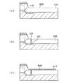
上述のように、図8に示したチップ990を例えば水平方向に5個、垂直方向に2個配列してバタブル組立を行うと、水平方向12.5cm、垂直方向10cmの非常に大きな受光面積を得ることができる。こうしたバタブル組立にあたっては、垂直方向でのチップ間の受光部として働かないデッドレイヤを小さくするために、各チップ9901〜99010のボンディングパッド部991は、水平な辺の一辺に揃えて配置されるが、高速動作が困難になる。本発明は、上記に鑑みてなされたものであり、大きな受光面積であっても高速動作可能な裏面照射型受光デバイスを提供する。
図1は本発明の一実施形態の裏面照射型受光デバイスの構成図である。
図1に示すように、この受光デバイスは、以下の要素を備えている。
(a)表面101側に電荷読み出し部110が形成された、シリコンを主材とする半導体薄板100。
(b)電荷読み出し部110の形成領域の周囲に形成され、電荷読み出し部110の周辺部を除いて、フィールド酸化膜200の表面202が露出されるとともに、露出領域にコンタクトホール205が形成されたフィールド酸化膜200。
(c)電荷読み出し部110上およびフィールド酸化膜の表面201上のコンタクトホール205の形成領域に至る領域上に形成されたポリシリコン配線300と、(d)半導体薄板100の表面101上のフィールド酸化膜200の表面201上に配設された補強部材400。
(d)半導体薄板100の表面102に形成されたアキュームレーション層510。
(e)アキュームレーション層510の表面上に形成された保護酸化膜520。
(f)フィールド酸化膜200のコンタクトホール205中およびフィールド酸化膜200の露出領域上に形成され、ポリシリコン配線300と電気的に接続するアルミニウム配線600(ボンディングパッド部610を含む)。
【0038】
ここで、補強部材として、硼硅酸ガラス(BSG)または硼リン硅酸ガラス(BPSG)を好適に採用できる。
【0039】
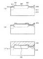
本実施形態の裏面照射型受光デバイスは、以下のようにして製造される。図2および図3は、本実施形態の裏面照射型受光デバイスの製造工程図である。
【0040】
まず、シリコンを主材とする半導体基板190の表面101に電荷読み出し部110を形成し、電荷読み出し部110の周囲の半導体基板190の表面101にフィールド酸化膜200を形成後、電荷読み出し部110上およびフィールド酸化膜200の表面201上に、選択的にポリシリコン配線300を施す(図2(a)参照)。
【0041】
次に、半導体基板190の表面101上およびフィールド酸化膜200の表面201に補強部材400を配設する(図2(b)参照)。補強部材400には、BSGまたはBPSGを好適に採用できる。そして、BSGまたはBPSGから成るガラス体を接着剤で貼り付けてもよいし、従来技術のようにBSGを堆積し焼結してもよい。
【0042】
引き続き、半導体基板190を加工して、半導体基板190を半導体薄板100とし、半導体薄板100の表面102上に保護酸化膜520を形成後、表面102側からイオン注入を行い、活性化して、アキュームレーション層510を形成する(図2(c)参照)。
【0043】
次いで、電荷読み出し部110の形成領域と電荷読み出し部110の近接領域とが形成する領域以外の半導体薄板100の構成材料を除去し、フィールド酸化膜200を露出させ(図3(a)参照)、フィールド酸化膜200の露出領域にポリシリコン配線300へ通じるコンタクトホール205を形成する(図3(b)参照)。
【0044】
そして、フィールド酸化膜200のコンタクトホール205中およびフィールド酸化膜200の露出領域上に、ポリシリコン配線300と電気的に接続するアルミニウム配線600(ボンディングパッド部610を含む)を施す。この後、ボンディングパッド部610にワイヤボンディングを施して、本実施形態の裏面照射型受光デバイスを得る。
【0045】
この製造方法では、アルミニウム配線600を施す工程の前に、高温処理を必要とする全ての工程、例えば、補強部材400の配設工程、保護酸化膜520の成長工程、およびイオン注入後の高温アニール工程などを完了する。
【0046】
したがって、受光側にアキュームレーション層510を形成しつつ、従来の半導体技術として確立した技術であるアルミニウム配線技術を使用して、アルミニウム配線600を施している。
【0047】
この結果、本実施形態の裏面照射型受光デバイスでは、受光側でアキュームレーションが可能となるので、電荷の収集効率が高くなるとともに、配線抵抗が小さいので高速動作が可能となる。
【0048】
【発明の効果】
以上、詳細に説明した通り、本発明の裏面照射型受光デバイスによれば、電荷読み出し部の電気信号の入出力を、電荷読み出し部近傍に形成され、配線長の短いポリシリコン配線と低抵抗のアルミニウム配線とを介して行う。したがって、従来に比べて格段に高速な動作が可能となる。
【0049】
また、本発明の裏面照射型受光デバイスの製造方法では、アルミニウム配線を施す工程の前に、高温処理を必要とする全ての工程、例えば、補強部材の配設工程、保護酸化膜の成長工程、およびイオン注入後の高温アニール工程などを完了する。したがって、従来の半導体技術として確立した技術であるアルミニウム配線を使用することが可能となり、本発明の裏面照射型受光デバイスを好適に製造できる。
【図面の簡単な説明】
【図1】本発明の一実施形態の裏面照射型受光デバイスの構成図である。
【図2】本発明の一実施形態の裏面照射型受光デバイスの製造工程図(前半)である。
【図3】本発明の一実施形態の裏面照射型受光デバイスの製造工程図(後半)である。
【図4】アキュームレーションの説明図である。
【図5】従来例の裏面照射型受光デバイスの構成図である。
【図6】従来例の裏面照射型受光デバイスの製造工程図(前半)である。
【図7】従来例の裏面照射型受光デバイスの製造工程図(後半)である。
【図8】バタブル組立の説明図である。
【符号の説明】
100…半導体薄板、110…電荷読み出し部、200…フィールド酸化膜、205…コンタクトホール、300…ポリシリコン配線、400…補強部材、510…アキュームレーション層、520…保護酸化膜、600…アルミニウム配線、610…ボンディングパッド部。[0001]
BACKGROUND OF THE INVENTION
The present invention relates to a back-illuminated charge coupled device (CCD) and a back-illuminated active pixel sensor that are effective for irradiation with energy rays having a large absorption coefficient such as ultraviolet rays, γ rays, or charged particle beams. The present invention relates to a backside illuminated light receiving device such as (Active Pixel Sensor; APS) and a method of manufacturing such a backside illuminated light receiving device.
[0002]
[Prior art]
In general, as a practical CCD image pickup device, there are three methods of frame transfer (FT), full frame transfer (FFT), and interline transfer (IT). A frame transfer method is used.
[0003]
The feature of the full frame transfer method is that there is no storage part and the area of the light receiving part can be increased, so that the light utilization rate is high and it is suitable for measurement of weak light. On the other hand, since the incident light can be absorbed by the charge transfer electrode, the sensitivity is significantly reduced for an input having a large absorption coefficient, for example, light having a short wavelength.
[0004]
In the structure of the light receiving part of a typical full frame transfer CCD, the polysilicon electrode covers the surface of the light receiving part without a gap, and a PSG film having a thickness of several μm is overlaid to separate each electrode. It has been. In particular, since polysilicon absorbs light and electrons having a wavelength of 400 nm or less, it cannot contribute to photoelectric conversion.
[0005]
With respect to such a photodetector, there is one in which the light receiving portion of the substrate is thinned from about 15 μm to about 20 μm and light is irradiated from the back surface. The photoelectric conversion portion is provided under the gate oxide film, and the polysilicon electrode 20 covers the gap without any gap and absorbs short wavelength light. However, there is no obstacle other than the thin oxide film on the back surface of the substrate. High sensitivity to short wavelength light can be expected. This back-illuminated CCD is sensitive to light having a short wavelength of about 200 nm, and is also applied to an electron impact type CCD imaging device. This device is expected as a high-sensitivity imaging device because it can utilize the signal charge multiplication effect caused by electron impact.
[0006]
The necessity of thinning in a backside illuminated light receiving device such as a backside illuminated CCD is as follows.
[0007]
As described above, in the backside illumination type light-receiving device, the back surface opposite to the surface of the substrate on which the charge reading unit or the like is formed is the light incident surface. On the other hand, most of light (ultraviolet light) having a large absorption coefficient and a wavelength of 200 to 300 nm is absorbed at a position slightly entering from the incident surface. Specifically, in the case of a silicon substrate, most of the incident light is absorbed up to a depth of 0.01 μm from the incident surface.
[0008]
Therefore, most of the photoelectrons generated in the vicinity of the back surface are lost due to recombination until they diffuse to the potential well of the CCD on the front surface. Even if the potential well is reached, the signals are mixed together while diffusing a long path of several hundreds of micrometers, and the resolution is significantly reduced.
[0009]
In addition, in the backside illumination type light receiving device, in addition to making the light receiving portion thin, it is necessary that a layer called an accumulation layer is formed on the back surface incident surface to form a potential slope. FIG. 4 is an explanatory diagram of accumulation. In FIG. 4, the left side represents the back surface and the right side represents the front surface. An
[0010]
However, the
[0011]
Formation of the accumulation layer is achieved by implanting boron into the
[0012]
In manufacturing a backside illuminated light receiving device, as described above, a manufacturing method that enables heat treatment such as formation of a growth oxide film and high temperature annealing after ion implantation, and a backside illuminated light receiving device manufactured by this manufacturing method, A technique (hereinafter referred to as a conventional example) disclosed in US Pat. No. 4,923,825 has been proposed.
[0013]
FIG. 5 is a configuration diagram of a backside illuminated light receiving device using a conventional technique. As shown in FIG. 5, this device includes (a) a semiconductor
[0014]
This back-illuminated light receiving device is manufactured as follows. 6 and 7 are manufacturing process diagrams of a conventional backside illuminated light receiving device.
[0015]
First, the
[0016]
Next, borosilicate glass is deposited on the surface formed by the
[0017]
Next, the periphery of the
[0018]
[Problems to be solved by the invention]
Since the conventional backside illuminated light receiving device is manufactured as described above, there are the following problems.
[0019]
The
[0020]
Therefore, aluminum having a melting point of about 660 ° C. cannot be used as a material for the
[0021]
Refractory metals such as current refractory metals or their silicides, in particular refractory metals, are more problematic than aluminum in terms of adhesion to the substrate, dry etching, and natural oxide film reduction at the contact portion. Therefore, it is difficult to proceed the process stably as when aluminum is used.
[0022]
The refractory metal silicide has better adhesion to the base and dry etching than the refractory metal itself. However, when a refractory metal silicide is used, the wiring resistance increases.
[0023]
Since a light receiving device for astronomical observation requires a large light receiving area, the wiring length becomes long. For example, if one pixel size is 12 μm × 12 μm, 2048 pixels in the horizontal direction and 4096 pixels in the vertical direction, the size of the chip is about 2.5 cm in the horizontal direction and about 5 cm in the vertical direction. End up.
[0024]
Further, as shown in FIG. 8, when five
[0025]
Since the typical sheet resistance of the refractory metal silicide wiring is 0.5Ω / □, assuming that the wiring width in the vertical direction is 20 μm and the wiring length is 5 cm, the wiring resistance is 1250Ω. If the wiring capacitance is 40 nF, the CR time constant is 50 μs, which makes high speed operation difficult.
[0026]
The present invention has been made in view of the above, and an object of the present invention is to provide a back-illuminated light receiving device that can operate at high speed even with a large light receiving area.
[0027]
Another object of the present invention is to provide a method for manufacturing a backside illuminated light receiving device that can suitably manufacture a backside illuminated light receiving device capable of high speed operation even with a large light receiving area.
[0028]
[Means for Solving the Problems]
According to a first aspect of the present invention, there is provided a backside illuminated light receiving device in which a charge readout portion having a one-dimensional or two-dimensional arrangement is formed on a first surface of a semiconductor thin plate mainly composed of silicon, and A back-side illuminated light receiving device in which chips for detecting the energy of electromagnetic waves or charged particles incident from the second surface, which is the back surface, are arranged, wherein the chip is (a) above the first surface of the semiconductor thin plate And (b) a surface that is formed in contact with the reinforcing member around the charge reading portion forming region and that faces the interface with the reinforcing member except at least the peripheral portion of the charge reading portion. A field oxide film that is exposed and has a contact hole formed in the exposed region; and (c) a charge readout portion at the interface between the charge readout portion and the reinforcing member of the field oxide film. Polysilicon wiring formed on the region reaching the contact hole forming region; (d) an accumulation layer formed on the second surface of the semiconductor thin plate; and (e) a contact hole in the field oxide film and the field oxide film. And an aluminum wiring electrically connected to the polysilicon wiring, and bonding pad portions included in the aluminum wiring of each chip are aligned on one side of the chip.
[0029]
Here, any one of borosilicate glass and borophosphosilicate glass can be suitably used as the reinforcing member.
[0030]
In the backside illuminated light receiving device according to claim 1, input / output of an electric signal of the charge readout portion is formed in the vicinity of the charge readout portion, and a polysilicon wiring having a short wiring length and a low resistance aluminum wiring (including a bonding pad) Do through. Since the sheet resistance of the aluminum wiring is about 2 × 10 −2 , even if the wiring width is 20 μm and the wiring length is 5 cm, the wiring resistance is 50Ω. When the wiring capacitance is 40 nF, the CR time constant is 2 μs, and the operation is much faster than in the past.
[0031]
According to a third aspect of the present invention, there is provided a backside illumination type light receiving device manufacturing method comprising: (a) a first step of forming a charge readout portion on a first surface of a semiconductor substrate mainly composed of silicon; A second step of forming a field oxide film on the first surface of the surrounding semiconductor substrate; (c) on the charge readout portion and on the first surface of the field oxide film corresponding to the first surface of the semiconductor substrate; A third step of selectively applying polysilicon wiring, and (d) a fourth step of disposing a reinforcing member on the first surface of the semiconductor substrate and on the first surface of the field oxide film, (E) a fifth step of processing the second surface of the semiconductor substrate to make the semiconductor substrate a semiconductor thin plate; and (f) ion implantation from the second surface side of the semiconductor thin plate to activate the accumulator. A sixth step of forming an isolation layer, and (g) charge A seventh step of removing the constituent material of the semiconductor thin plate other than the region where the protruding portion is formed and the adjacent region of the charge readout portion to expose the field oxide film, and (h) the polysilicon wiring in the exposed region of the field oxide film An eighth step of forming a contact hole to communicate with, and (i) a ninth step of applying an aluminum wiring electrically connected to the polysilicon wiring in the contact hole of the field oxide film and on the exposed region of the field oxide film; It is characterized by providing.
[0032]
Here, the fourth step may be (i) a step of attaching a reinforcing member to a surface formed by the first surface of the semiconductor substrate and the first surface of the field oxide film. (Ii) The step of depositing the reinforcing member material on the surface formed by the first surface of the semiconductor substrate and the first surface of the field oxide film may be employed.
[0033]
In addition, any one of borosilicate glass and borophosphosilicate glass can be suitably employed as the reinforcing member.
[0034]
In the method of manufacturing the backside illuminated light receiving device according to claim 3, all the steps that require high temperature treatment, for example, the step of disposing the reinforcing member 940 (first step) before the step of applying aluminum wiring (the ninth step). Step 4), a protective oxide film growth step (fifth step), a high-temperature annealing step after ion implantation (sixth step), and the like are completed.
[0035]
Therefore, it is possible to use aluminum wiring, which is a technique established as a conventional semiconductor technique, while forming an accumulation layer on the light receiving side, and the backside illuminated light receiving device according to claim 1 is preferably manufactured.
The backside illuminated light receiving device according to claim 7 includes a semiconductor thin plate having a charge readout portion on the first surface and a field oxide film provided around the charge readout portion, and an accumulation layer on the second surface. In the backside illumination type light receiving device in which chips each having a reinforcing member disposed on the first surface are arranged, the chip is a polysilicon wiring extending from the charge readout portion to the interface between the field oxide film and the reinforcing member. And an aluminum wiring electrically connected to the polysilicon wiring through a contact hole provided in the field oxide film, and bonding pad portions included in the aluminum wiring of each chip are aligned on one side of the chip It is characterized by.
The manufacturing method of the backside illuminated light receiving device according to claim 8 is characterized in that the accumulation layer is activated after the formation of the polysilicon wiring, and then the aluminum wiring is formed.
[0036]
DETAILED DESCRIPTION OF THE INVENTION
Embodiments of a backside illumination type light receiving device and a manufacturing method of the backside illumination type light receiving device of the present invention will be described below with reference to the accompanying drawings. In the description of the drawings, the same elements are denoted by the same reference numerals, and redundant description is omitted.
[0037]
As described above, for example, when five
FIG. 1 is a configuration diagram of a backside illuminated light receiving device according to an embodiment of the present invention.
As shown in FIG. 1, the light receiving device includes the following elements.
(A) A semiconductor
(B) The
(C)
(D) An
(E) A
(F) Aluminum wiring 600 (including bonding pad portion 610) formed in
[0038]
Here, borosilicate glass (BSG) or borophosphosilicate glass (BPSG) can be suitably employed as the reinforcing member.
[0039]
The backside illumination type light receiving device of this embodiment is manufactured as follows. 2 and 3 are manufacturing process diagrams of the backside illumination type light receiving device of this embodiment.
[0040]
First, the
[0041]
Next, the reinforcing
[0042]
Subsequently, the
[0043]
Next, the constituent material of the semiconductor
[0044]
Then, in the
[0045]
In this manufacturing method, before the step of applying the
[0046]
Therefore, while forming the
[0047]
As a result, in the backside illuminated light receiving device of this embodiment, accumulation is possible on the light receiving side, so that the charge collection efficiency is increased and the wiring resistance is small, so that high speed operation is possible.
[0048]
【The invention's effect】
As described above in detail, according to the backside illuminated light receiving device of the present invention, the input / output of the electrical signal of the charge readout part is formed in the vicinity of the charge readout part, and the polysilicon wiring having a short wiring length and the low resistance are provided. This is done via aluminum wiring. Therefore, the operation can be performed much faster than in the past.
[0049]
Further, in the method of manufacturing the backside illuminated light receiving device of the present invention, before the step of applying the aluminum wiring, all the steps that require high temperature treatment, for example, the step of arranging the reinforcing member, the step of growing the protective oxide film, And the high-temperature annealing process after ion implantation is completed. Therefore, it is possible to use aluminum wiring, which is a technique established as a conventional semiconductor technique, and the backside illumination type light receiving device of the present invention can be suitably manufactured.
[Brief description of the drawings]
FIG. 1 is a configuration diagram of a backside illuminated light receiving device according to an embodiment of the present invention.
FIG. 2 is a manufacturing process diagram (first half) of a backside illuminated light receiving device according to an embodiment of the present invention.
FIG. 3 is a manufacturing process diagram (second half) of a backside illuminated light receiving device according to an embodiment of the present invention;
FIG. 4 is an explanatory diagram of accumulation.
FIG. 5 is a configuration diagram of a backside illuminated light receiving device of a conventional example.
FIG. 6 is a manufacturing process diagram (first half) of a conventional backside illuminated light receiving device.
FIG. 7 is a manufacturing process diagram (second half) of a conventional backside illuminated light receiving device;
FIG. 8 is an explanatory view of a batable assembly.
[Explanation of symbols]
DESCRIPTION OF
Claims (8)
前記チップは、
前記半導体薄板の第1の表面上側に配設された補強部材と、
前記電荷読み出し部の形成領域の周囲の前記補強部材に接して形成され、少なくとも前記電荷読み出し部の周辺部を除いて、前記補強部材との界面に対向する表面が露出されるとともに、露出領域にコンタクトホールが形成されたフィールド酸化膜と、
前記電荷読み出し部上および前記フィールド酸化膜の前記補強部材との界面の前記電荷読み出し部からコンタクトホール形成領域に至る領域上に形成されたポリシリコン配線と、
前記半導体薄板の第2の表面に形成されたアキュームレーション層と、
前記フィールド酸化膜のコンタクトホール中および前記フィールド酸化膜の露出領域上に形成され、前記ポリシリコン配線と電気的に接続するアルミニウム配線と、
を備え、
各前記チップの前記アルミニウム配線に含まれるボンディングパッド部を前記チップの一辺に揃えてなることを特徴とする裏面照射型受光デバイス。A charge readout portion having a one-dimensional or two-dimensional arrangement is formed on a first surface of a semiconductor thin plate mainly made of silicon, and a second surface that is the back surface of the first surface of the semiconductor thin plate A back-illuminated light receiving device in which chips for detecting the energy of electromagnetic waves or charged particles incident from are arranged,
The chip is
A reinforcing member disposed above the first surface of the semiconductor thin plate;
The surface that is formed in contact with the reinforcing member around the charge reading portion forming region and that faces at least the peripheral portion of the charge reading portion and faces the interface with the reinforcing member is exposed, and is exposed to the exposed region. A field oxide film in which contact holes are formed;
A polysilicon wiring formed on the charge reading portion and on a region extending from the charge reading portion to a contact hole forming region at an interface between the field oxide film and the reinforcing member;
An accumulation layer formed on the second surface of the semiconductor sheet;
An aluminum wiring formed in a contact hole of the field oxide film and on an exposed region of the field oxide film, and electrically connected to the polysilicon wiring;
With
A backside illuminated light receiving device, wherein bonding pads included in the aluminum wiring of each chip are aligned on one side of the chip.
前記電荷読み出し部の周囲の前記半導体基板の第1の表面上にフィールド酸化膜を形成する第2の工程と、
前記電荷読み出し部上および前記半導体基板の第1の表面側に応じた前記フィールド酸化膜の第1の表面上に、選択的にポリシリコン配線を施す第3の工程と、
前記半導体基板の第1の表面上および前記フィールド酸化膜の第1の表面上に補強部材を配設する第4の工程と、
前記半導体基板の第2の表面を加工して、前記半導体基板を半導体薄板とする第5の工程と、
前記半導体薄板の第2の表面側からイオン注入を行い、活性化して、アキュームレーション層を形成する第6の工程と、
前記電荷読み出し部の形成領域と前記電荷読み出し部の近接領域以外の前記半導体薄板の構成材料を除去し、前記フィールド酸化膜を露出させる第7の工程と、
前記フィールド酸化膜の露出領域に前記ポリシリコン配線へ通じるコンタクトホールを形成する第8の工程と、
前記フィールド酸化膜のコンタクトホール中および前記フィールド酸化膜の露出領域上に、前記ポリシリコン配線と電気的に接続するアルミニウム配線を施す第9の工程と、
を備えることを特徴とする裏面照射型受光デバイスの製造方法。A first step of forming a charge readout portion on a first surface of a semiconductor substrate mainly composed of silicon;
A second step of forming a field oxide film on the first surface of the semiconductor substrate around the charge readout portion;
A third step of selectively applying polysilicon wiring on the charge readout portion and on the first surface of the field oxide film corresponding to the first surface side of the semiconductor substrate;
A fourth step of disposing a reinforcing member on the first surface of the semiconductor substrate and on the first surface of the field oxide film;
Processing a second surface of the semiconductor substrate to make the semiconductor substrate a semiconductor thin plate; and
A sixth step of performing ion implantation from the second surface side of the semiconductor thin plate and activating to form an accumulation layer;
A seventh step of removing the constituent material of the semiconductor thin plate other than the formation region of the charge readout portion and the adjacent region of the charge readout portion to expose the field oxide film;
An eighth step of forming a contact hole leading to the polysilicon wiring in the exposed region of the field oxide film;
A ninth step of applying an aluminum wiring electrically connected to the polysilicon wiring in a contact hole of the field oxide film and on an exposed region of the field oxide film;
A method for producing a backside illuminated light receiving device.
前記電荷読み出し部から前記フィールド酸化膜と前記補強部材との界面に至るポリシリコン配線と、前記フィールド酸化膜に設けられたコンタクトホールを介して前記ポリシリコン配線に電気的に接続されたアルミニウム配線とを備え、各前記チップの前記アルミニウム配線に含まれるボンディングパッド部を前記チップの一辺に揃えてなることを特徴とする裏面照射型受光デバイス。A semiconductor thin plate having a charge readout portion on the first surface and a field oxide film provided around the charge readout portion and having an accumulation layer on the second surface; and a reinforcing member disposed on the first surface; In a back-illuminated light-receiving device formed by arranging chips equipped with
Polysilicon wiring extending from the charge readout portion to the interface between the field oxide film and the reinforcing member, and aluminum wiring electrically connected to the polysilicon wiring through a contact hole provided in the field oxide film; A back-illuminated light-receiving device, wherein a bonding pad portion included in the aluminum wiring of each chip is aligned on one side of the chip.
Priority Applications (4)
| Application Number | Priority Date | Filing Date | Title |
|---|---|---|---|
| JP27000696A JP3620936B2 (en) | 1996-10-11 | 1996-10-11 | Back-illuminated light receiving device and manufacturing method thereof |
| EP97308026A EP0836231B1 (en) | 1996-10-11 | 1997-10-10 | Method of making a back irradiation type light-receiving device |
| DE69737492T DE69737492T2 (en) | 1996-10-11 | 1997-10-10 | Process for the preparation of a photosensitive component with back radiation incidence |
| US08/948,822 US6031274A (en) | 1996-10-11 | 1997-10-10 | Back irradiation type light-receiving device and method of making the same |
Applications Claiming Priority (1)
| Application Number | Priority Date | Filing Date | Title |
|---|---|---|---|
| JP27000696A JP3620936B2 (en) | 1996-10-11 | 1996-10-11 | Back-illuminated light receiving device and manufacturing method thereof |
Publications (2)
| Publication Number | Publication Date |
|---|---|
| JPH10116974A JPH10116974A (en) | 1998-05-06 |
| JP3620936B2 true JP3620936B2 (en) | 2005-02-16 |
Family
ID=17480247
Family Applications (1)
| Application Number | Title | Priority Date | Filing Date |
|---|---|---|---|
| JP27000696A Expired - Lifetime JP3620936B2 (en) | 1996-10-11 | 1996-10-11 | Back-illuminated light receiving device and manufacturing method thereof |
Country Status (4)
| Country | Link |
|---|---|
| US (1) | US6031274A (en) |
| EP (1) | EP0836231B1 (en) |
| JP (1) | JP3620936B2 (en) |
| DE (1) | DE69737492T2 (en) |
Families Citing this family (26)
| Publication number | Priority date | Publication date | Assignee | Title |
|---|---|---|---|---|
| JP4373695B2 (en) * | 2003-04-16 | 2009-11-25 | 浜松ホトニクス株式会社 | Manufacturing method of backside illuminated photodetector |
| US7901989B2 (en) | 2006-10-10 | 2011-03-08 | Tessera, Inc. | Reconstituted wafer level stacking |
| US7829438B2 (en) * | 2006-10-10 | 2010-11-09 | Tessera, Inc. | Edge connect wafer level stacking |
| US8513789B2 (en) | 2006-10-10 | 2013-08-20 | Tessera, Inc. | Edge connect wafer level stacking with leads extending along edges |
| US7791199B2 (en) * | 2006-11-22 | 2010-09-07 | Tessera, Inc. | Packaged semiconductor chips |
| US8569876B2 (en) | 2006-11-22 | 2013-10-29 | Tessera, Inc. | Packaged semiconductor chips with array |
| US7952195B2 (en) * | 2006-12-28 | 2011-05-31 | Tessera, Inc. | Stacked packages with bridging traces |
| CN101675516B (en) * | 2007-03-05 | 2012-06-20 | 数字光学欧洲有限公司 | Chips having rear contacts connected by through vias to front contacts |
| WO2009017758A2 (en) * | 2007-07-27 | 2009-02-05 | Tessera, Inc. | Reconstituted wafer stack packaging with after-applied pad extensions |
| KR101538648B1 (en) | 2007-07-31 | 2015-07-22 | 인벤사스 코포레이션 | Semiconductor packaging process using through silicon vias |
| CN101861646B (en) | 2007-08-03 | 2015-03-18 | 泰塞拉公司 | Stack packages using reconstituted wafers |
| US8043895B2 (en) * | 2007-08-09 | 2011-10-25 | Tessera, Inc. | Method of fabricating stacked assembly including plurality of stacked microelectronic elements |
| US20090212381A1 (en) * | 2008-02-26 | 2009-08-27 | Tessera, Inc. | Wafer level packages for rear-face illuminated solid state image sensors |
| US20100053407A1 (en) * | 2008-02-26 | 2010-03-04 | Tessera, Inc. | Wafer level compliant packages for rear-face illuminated solid state image sensors |
| JP5639052B2 (en) * | 2008-06-16 | 2014-12-10 | テッセラ,インコーポレイテッド | Edge stacking at wafer level |
| WO2010104610A2 (en) * | 2009-03-13 | 2010-09-16 | Tessera Technologies Hungary Kft. | Stacked microelectronic assemblies having vias extending through bond pads |
| US8791575B2 (en) | 2010-07-23 | 2014-07-29 | Tessera, Inc. | Microelectronic elements having metallic pads overlying vias |
| US8796135B2 (en) | 2010-07-23 | 2014-08-05 | Tessera, Inc. | Microelectronic elements with rear contacts connected with via first or via middle structures |
| US9640437B2 (en) | 2010-07-23 | 2017-05-02 | Tessera, Inc. | Methods of forming semiconductor elements using micro-abrasive particle stream |
| US8610259B2 (en) | 2010-09-17 | 2013-12-17 | Tessera, Inc. | Multi-function and shielded 3D interconnects |
| US8847380B2 (en) | 2010-09-17 | 2014-09-30 | Tessera, Inc. | Staged via formation from both sides of chip |
| KR101059490B1 (en) | 2010-11-15 | 2011-08-25 | 테세라 리써치 엘엘씨 | Conductive pads defined by embedded traces |
| US8587126B2 (en) | 2010-12-02 | 2013-11-19 | Tessera, Inc. | Stacked microelectronic assembly with TSVs formed in stages with plural active chips |
| US8637968B2 (en) | 2010-12-02 | 2014-01-28 | Tessera, Inc. | Stacked microelectronic assembly having interposer connecting active chips |
| US8736066B2 (en) | 2010-12-02 | 2014-05-27 | Tessera, Inc. | Stacked microelectronic assemby with TSVS formed in stages and carrier above chip |
| US8610264B2 (en) | 2010-12-08 | 2013-12-17 | Tessera, Inc. | Compliant interconnects in wafers |
Family Cites Families (6)
| Publication number | Priority date | Publication date | Assignee | Title |
|---|---|---|---|---|
| JPS54110068U (en) * | 1978-01-20 | 1979-08-02 | ||
| US4870475A (en) * | 1985-11-01 | 1989-09-26 | Nec Corporation | Semiconductor device and method of manufacturing the same |
| US4892842A (en) * | 1987-10-29 | 1990-01-09 | Tektronix, Inc. | Method of treating an integrated circuit |
| US4923825A (en) * | 1989-05-01 | 1990-05-08 | Tektronix, Inc. | Method of treating a semiconductor body |
| JPH06326293A (en) * | 1993-05-12 | 1994-11-25 | Hamamatsu Photonics Kk | Photodetector |
| JP3183390B2 (en) * | 1995-09-05 | 2001-07-09 | キヤノン株式会社 | Photoelectric conversion device and imaging device using the same |
-
1996
- 1996-10-11 JP JP27000696A patent/JP3620936B2/en not_active Expired - Lifetime
-
1997
- 1997-10-10 EP EP97308026A patent/EP0836231B1/en not_active Expired - Lifetime
- 1997-10-10 US US08/948,822 patent/US6031274A/en not_active Expired - Lifetime
- 1997-10-10 DE DE69737492T patent/DE69737492T2/en not_active Expired - Lifetime
Also Published As
| Publication number | Publication date |
|---|---|
| EP0836231A3 (en) | 1998-11-11 |
| DE69737492D1 (en) | 2007-05-03 |
| JPH10116974A (en) | 1998-05-06 |
| EP0836231B1 (en) | 2007-03-21 |
| DE69737492T2 (en) | 2007-11-29 |
| EP0836231A2 (en) | 1998-04-15 |
| US6031274A (en) | 2000-02-29 |
Similar Documents
| Publication | Publication Date | Title |
|---|---|---|
| JP3620936B2 (en) | Back-illuminated light receiving device and manufacturing method thereof | |
| JP3924352B2 (en) | Backside illuminated light receiving device | |
| JP5185205B2 (en) | Semiconductor photo detector | |
| TWI267982B (en) | Solid-state imaging device and method for manufacturing the same | |
| JP3759435B2 (en) | XY address type solid-state imaging device | |
| US5670817A (en) | Monolithic-hybrid radiation detector/readout | |
| JPH0135549B2 (en) | ||
| EP0616373A2 (en) | Photoelectric conversion semiconductor device and method of manufacturing the same | |
| JP5829224B2 (en) | MOS image sensor | |
| JP2009507392A (en) | Backside thinned image sensor with integrated lens stack | |
| US7810740B2 (en) | Back illuminated photodiode array, manufacturing method and semiconductor device thereof | |
| JP2797984B2 (en) | Solid-state imaging device and method of manufacturing the same | |
| JP2008514011A (en) | Manufacturing method of back-illuminated CMOS or CCD image sensor (IMAGER) made of SOI wafer | |
| JP4258875B2 (en) | Photoelectric conversion element and photoelectric conversion device | |
| JP2004031452A (en) | Rear face incident type imaging device | |
| JP2002314061A (en) | Solid-state image sensing device and its manufacturing method | |
| US5270221A (en) | Method of fabricating high quantum efficiency solid state sensors | |
| EP1569275B1 (en) | Backside-illuminated photodiode array, method for manufacturing same, and semiconductor device | |
| TW200822350A (en) | Method and apparatus for reducing smear in back-illuminated imaging sensors | |
| JP3049015B2 (en) | Active pixel cell with bandgap design | |
| JP2866328B2 (en) | Solid-state imaging device | |
| JP4397989B2 (en) | Semiconductor energy detector | |
| JPH08316450A (en) | Multilayer solid-state image pickup device and its manufacture | |
| JP4562875B2 (en) | Semiconductor device | |
| JPH05152551A (en) | Manufacture of solid-state imaging device |
Legal Events
| Date | Code | Title | Description |
|---|---|---|---|
| A02 | Decision of refusal |
Free format text: JAPANESE INTERMEDIATE CODE: A02 Effective date: 20040510 |
|
| A521 | Request for written amendment filed |
Free format text: JAPANESE INTERMEDIATE CODE: A523 Effective date: 20040708 |
|
| A521 | Request for written amendment filed |
Free format text: JAPANESE INTERMEDIATE CODE: A523 Effective date: 20040902 |
|
| A911 | Transfer to examiner for re-examination before appeal (zenchi) |
Free format text: JAPANESE INTERMEDIATE CODE: A911 Effective date: 20040908 |
|
| TRDD | Decision of grant or rejection written | ||
| A01 | Written decision to grant a patent or to grant a registration (utility model) |
Free format text: JAPANESE INTERMEDIATE CODE: A01 Effective date: 20041109 |
|
| A61 | First payment of annual fees (during grant procedure) |
Free format text: JAPANESE INTERMEDIATE CODE: A61 Effective date: 20041116 |
|
| R150 | Certificate of patent or registration of utility model |
Free format text: JAPANESE INTERMEDIATE CODE: R150 |
|
| S531 | Written request for registration of change of domicile |
Free format text: JAPANESE INTERMEDIATE CODE: R313532 |
|
| R350 | Written notification of registration of transfer |
Free format text: JAPANESE INTERMEDIATE CODE: R350 |
|
| FPAY | Renewal fee payment (event date is renewal date of database) |
Free format text: PAYMENT UNTIL: 20081126 Year of fee payment: 4 |
|
| FPAY | Renewal fee payment (event date is renewal date of database) |
Free format text: PAYMENT UNTIL: 20081126 Year of fee payment: 4 |
|
| FPAY | Renewal fee payment (event date is renewal date of database) |
Free format text: PAYMENT UNTIL: 20091126 Year of fee payment: 5 |
|
| FPAY | Renewal fee payment (event date is renewal date of database) |
Free format text: PAYMENT UNTIL: 20091126 Year of fee payment: 5 |
|
| FPAY | Renewal fee payment (event date is renewal date of database) |
Free format text: PAYMENT UNTIL: 20101126 Year of fee payment: 6 |
|
| FPAY | Renewal fee payment (event date is renewal date of database) |
Free format text: PAYMENT UNTIL: 20111126 Year of fee payment: 7 |
|
| FPAY | Renewal fee payment (event date is renewal date of database) |
Free format text: PAYMENT UNTIL: 20121126 Year of fee payment: 8 |
|
| FPAY | Renewal fee payment (event date is renewal date of database) |
Free format text: PAYMENT UNTIL: 20131126 Year of fee payment: 9 |
|
| EXPY | Cancellation because of completion of term |