JP3617618B2 - Manufacturing method of semiconductor laser device - Google Patents
Manufacturing method of semiconductor laser device Download PDFInfo
- Publication number
- JP3617618B2 JP3617618B2 JP36195099A JP36195099A JP3617618B2 JP 3617618 B2 JP3617618 B2 JP 3617618B2 JP 36195099 A JP36195099 A JP 36195099A JP 36195099 A JP36195099 A JP 36195099A JP 3617618 B2 JP3617618 B2 JP 3617618B2
- Authority
- JP
- Japan
- Prior art keywords
- film
- protective film
- angstrom
- laser
- thickness
- Prior art date
- Legal status (The legal status is an assumption and is not a legal conclusion. Google has not performed a legal analysis and makes no representation as to the accuracy of the status listed.)
- Expired - Fee Related
Links
Images


Landscapes
- Semiconductor Lasers (AREA)
Description
【0001】
【発明の属する技術分野】
本発明は、レーザチップの端面に所定の反射率を有する保護膜を設けた半導体レーザ素子およびその製造方法に関し、特に、高い信頼性を有する半導体レーザ素子に適した保護膜を得ることができる半導体レーザ素子およびその製造方法に関する。
【0002】
【従来の技術】
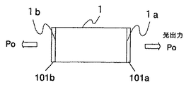
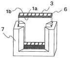
半導体レーザ素子においては、図3に示すように、GaAsレーザチップ1の両端面1a、1bに等しい反射率を有する保護膜101a、101bが設けられている構成のものが多い。この場合、両端面からの光出力Poは等しくなる。
【0003】
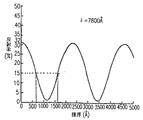
この保護膜101aがAl2O3からなる場合、例えばAl2O3膜の屈折率(n)をn=1.60、レーザチップ1の屈折率をn=3.50として計算すると、保護膜101aの膜厚dを変化させることによって、図4に示すように、保護膜101aの反射率が変化する。なお、この図4では、レーザ発振波長(λ)7800オングストロームでの計算結果を示している。
【0004】
この図4に示すように、保護膜の厚さに関わらず、反射率は保護膜が無い場合よりも小さくなる。そして、光学的膜厚n×dが発振波長の1/4の奇数倍になったときに反射率が最小となり、光学的膜厚n×dが発振波長の1/2の整数倍になったときに保護膜が無い場合とほぼ同じ反射率となる。これは、Al2O3保護膜101aの屈折率がGaAsレーザチップ1の屈折率よりも小さいためである。
【0005】
これに対して、GaAsレーザチップ1の屈折率よりも大きい屈折率を有する膜、例えばアモルファスSi等の膜を用いた場合、保護膜の厚さに関わらず、反射率は保護膜が無い場合よりも大きくなる。そして、光学的膜厚n×dが発振波長の1/4の奇数倍になったときに反射率が最大となり、光学的膜厚n×dが発振波長の1/2の整数倍になったときに保護膜が無い場合とほぼ同じ反射率となる。
【0006】
ところで、光出力20mW以上の高出力レーザの場合には、一般に、図5に示すように、主出射面(前面)側からの光出力Pfを高くするために、前面側1aを保護膜が無い場合の反射率よりも低い反射率となるように、その反対側(後面)側1bを保護膜が無い場合よりも高い反射率となるように設計している。
【0007】
例えば、前面側1aのAl2O3保護膜201aは膜厚を約700オングストローム〜1600オングストロームに形成することにより、その反射率を約15%以下に設定することができる。一方、後面側1bの保護膜100は、レーザチップ1の屈折率よりも大きい屈折率を有する膜を用いても、1層では十分に高い反射率が得られない。このため、第1層および第3層102bとして厚さλ/4(λ:波長)に相当するAl2O3膜、第2層および第4層104bとして厚さλ/4に相当するアモルファスSi膜を交互に積層し、最後の第5層103bとして厚さλ/2に相当するAl2O3膜を積層する。これにより、約85%以上の高反射率の保護膜を形成することができる。
【0008】
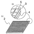
以下に、レーザチップの端面に上述したような所定の反射率を有する保護膜を形成する方法を説明する。まず、図6(a)および図6(b)に示すように、レーザウェハ2における特定の素子の電極3とそれに隣接する素子の電極3との間に、発光部(チャネル)4と直交する方向に、劈開線5をスクライブにより形成する。次に、図7に示すように、ウェハ2を劈開して、レーザバー(バー状態のレーザチップ)6を形成する。
【0009】
次に、図8に示すように、レーザバー6を、レーザバー固定用治具7に電極3面を重ねるようにしてセットする。このとき、全てのレーザバー6においてレーザチップの前面(主出射面)1a側および後面1b側が同じ向きとなるようにセットする。
【0010】
次に、レーザバー固定用治具7に固定されたレーザバー6の端面に所定の反射率を有する保護膜を成膜する。この成膜には、一般に、図9に示すような真空蒸着装置が用いられる。この真空蒸着装置は、チャンバー9内に蒸着源11と上記レーザバー固定用治具7を保持するためのホルダー8と蒸着膜厚モニター用の水晶振動子14を備えている。
【0011】
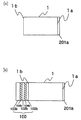
この装置を用いてレーザチップの両端面1a、1bに保護膜を蒸着する場合、まず、図9に示すように、ダクト10を通してチャンバー9内を真空にする。そして、所定の真空度に達した後、蒸着源11に入れた蒸着材料12を電子ビーム等で加熱して蒸発させて、図10(a)に示すようにレーザチップ1の端面1aに保護膜101aを蒸着する。蒸着完了後、引き続いてホルダー8を180゜回転させ、図1(b)に示すようにレーザチップ1のもう一方の端面1bに保護膜101bを蒸着する。両端面1a、1bに保護膜を形成するときの成膜速度(蒸着レート)は、蒸着完了までの間、ほぼ一定となるように制御される。この蒸着レートは加熱温度により制御されるので、電子ビーム蒸着の場合には電子ビームの強度により制御される。また、抵抗加熱の場合には、抵抗体に流す電流量で制御されることは良く知られている。この蒸着レートは、蒸着材料がAl2O3の場合、数オングストローム/秒〜30オングストローム/秒の間で設定されるのが一般的である。なお、蒸着は水晶振動子14にて膜厚をモニターしながら行い、所定の膜厚に達した時点で蒸着を停止する。
【0012】
さらに、高出力タイプの半導体レーザ素子の場合には、上述した手順と同様にして、図11(a)に示すように、前面(主出射面)1a側に反射率約15%以下の低反射保護膜201aを成膜した後、引き続いて図11(b)に示すように、後面1b側に高反射保護膜100を成膜する。この高反射保護膜100は、上述したように、第1層および第3層102bとして厚さλ/4(λ:波長)に相当するAl2O3膜、第2層および第4層104bとして厚さλ/4に相当するアモルファスSi膜を交互に積層し、最後の第5層103bとして厚さλ/2に相当するAl2O3膜を積層する。
【0013】
【発明が解決しようとする課題】
上述したように、レーザチップの端面に保護膜を形成する場合、保護膜の成膜速度は蒸着完了までの間、一定となるように制御される。よって、図9に示したように、蒸着材料12に入力される電子ビームパワー13も蒸着完了までの間、ほぼ一定となる。しかし、このようにして作製した半導体レーザ素子を高出力で動作させると、必要とされる信頼性が得られないという問題があった。
【0014】
本発明は、このような従来技術の問題点を解決すべくなされたものであり、レーザチップの端面に所定の反射率の保護膜を有し、信頼性の高い半導体レーザ素子およびその製造方法を提供することを目的とする。
【0015】
【課題を解決するための手段】
本発明の半導体レーザ素子の製造方法は、多数のレーザチップが形成されたレーザウェハを劈開して、複数のレーザチップがバー状態になったレーザバーを、各レーザチップのそれぞれの端面が両側に露出した状態で形成し、該レーザバーをバー固定用治具により保持して、該レーザバーにおける各レーザチップのそれぞれの端面に所定の反射率を有する所定の膜厚Tの保護膜を成膜する成膜工程を包含する半導体レーザ素子の製造方法において、前記成膜工程が、前記保護膜としてAl2O3膜を、電子ビーム蒸着法によって、5オングストローム/秒以上10オングストローム/秒以下の成膜速度rで、前記膜厚Tの1/5以上1/2以下に達するまで成膜する第1成膜工程と、該第1成膜工程に連続して、Al2O3膜を、前記膜厚Tに達するまで10オングストローム/秒以上20オングストローム/秒以下の成膜速度Rであってr<Rの条件で成膜する第2工程と、を包含すること特徴とし、そのことにより上記目的が達成される。
【0016】
好ましくは、前記第1の成膜工程の成膜速度が5オングストローム/秒であり、前記第2の成膜工程の成膜速度が10オングストローム/秒である。
【0017】
好ましくは、前記膜厚Tが1500オングストロームであり、前記第1の成膜工程における膜厚が、300オングストロームである。
【0018】
好ましくは、前記レーザバーにおける各レーザチップの一方の端面に成膜されたAl 2 O 3 膜上に、アモルファスSi膜とAl 2 O 3 膜とを交互に積層する第3成膜工程をさらに包含する。
【0024】
以下、本発明の作用について説明する。
【0025】
本発明にあっては、レーザチップの端面に所定の反射率を有する保護膜を成膜する際に、ある膜厚に達するまでを比較的低い成膜速度で成膜するので、レーザチップ端面に与えるダメージを小さくすることが可能である。また、残りの所定膜厚までをそれよりも速い成膜速度で成膜するので、緻密で大気中の水分や酸素を通しにくい、良好な膜質の保護膜を得ることが可能である。
【0026】
両端面に所定の反射率を有する保護膜を成膜した後、一方の端面(後面側)の保護膜上に多層膜を成膜して後面側を高反射率とすることにより、高出力の半導体レーザ素子にも適用可能である。
【0027】
GaAsレーザチップの場合、保護膜の材料としては例えばAl2O3を用いることができる。また、その上に成膜する多層膜としては、例えばアモルファスSiとAl2O3を交互に積層したものを用いることができる。この保護膜の成膜速度は、電子ビーム蒸着の場合、電子ビームの強度により制御することが可能である。そして、蒸発に寄与しない電子流の量を低くした条件下で端面近傍の保護膜を成膜可能であるので、光出射端面に与えるダメージが小さくなる。
【0028】
半導体レーザ素子の端面保護膜の形成方法において、保護膜がある膜厚に達するまでをある成膜速度で成膜し、残りの所定膜厚までをその2倍の成膜速度で成膜すると、半導体レーザ素子のCOD(光学的破壊レベル)は、従来方法により成膜品と比較して高くなるので好ましい。また、保護膜がある膜厚に達するまでを5オングストローム/秒以上10オングストローム/秒以下の成膜速度で成膜し、残りの所定膜厚までを10オングストローム/秒以上20オングストローム/秒以下の成膜速度で成膜すると、さらに半導体レーザ素子のCOD値が高くなるので好ましい。さらに、保護膜が所定膜厚の1/5以上1/2以下に達するまでをある成膜速度で成膜し、残りの所定膜厚までをそれよりも速い成膜速度で成膜すると、半導体レーザ素子のCOD値が従来方法による成膜品と比較して高くなるので好ましい。
【0029】
【発明の実施の形態】
まず、本発明の原理について簡単に説明する。
【0030】
レーザチップの端面に比較的高い成膜速度、例えば約10オングストローム/秒〜30オングストローム/秒程度で保護膜を成膜した場合、膜質が緻密で大気中の水分や酸素を通しにくく、端面の劣化を防止する効果の大きい保護膜が得られると考えられる。
【0031】
しかし、この場合、図9に示した蒸着材料12に入力する電子ビームパワー13も高くなるため、蒸着に寄与しない迷走電子や反跳電子等の電子流15が増加し、それがレーザチップ端面にダメージを与えて半導体レーザ素子としての信頼性が損なわれるおそれがある。また、保護膜材料の飛散速度も速くなるので、保護膜材料自身によりレーザチップ端面にダメージを与えるおそれもある。さらに、熱膨張率の大きく異なるレーザチップと保護膜との密着性が良いため、レーザ発振時には端面の温度が高くなり、熱応力によってレーザチップを構成している結晶にダメージを与えることも考えられる。
【0032】
一方、保護膜の成膜速度を比較的低い条件、例えば10オングストローム/秒程度以下とした場合、保護膜の膜質を良好なものにすることが困難であり、半導体レーザ素子としての信頼性を損なうおそれがある。
【0033】
本発明はこのような考察に基づいてなされたものである。以下に、本発明の実施形態について、図面を参照しながら説明する。
【0034】
(実施形態1)
図1は、本実施形態1における半導体レーザ素子の製造方法を説明するための図である。本実施形態では、図1(b−4)に示すように、レーザチップ1の一方の端面1a側に、所定の反射率を有し、その組成が一定で、所定膜厚Tのうち、端面1aからある膜厚までの部分301aの密度が残りの部分302aの密度よりも低い保護膜が所定膜厚Tで形成している。また、他方の端面1b側には、所定の反射率を有し、その組成が一定で、所定膜厚Tのうち、端面1bからある膜厚までの部分301bの密度が残りの部分302bの密度よりも低い保護膜を形成している。
【0035】
この半導体レーザ素子の製造は、以下のようにして行うことができる。まず、従来技術と同様に、図6に示したようなウェハ2を劈開して図7に示したようなバー状態のレーザチップ6を形成し、図8に示したようにそのバー状態のレーザチップ6をバー固定用治具7に電極3面を重ねるようにしてセットする。このとき、全てのレーザバー6においてレーザチップの端面1a側および端面1b側が同じ向きとなるようにセットする。そして、レーザバー固定用治具7に固定されたレーザバー6の端面1a、1bに所定の反射率を有する保護膜を成膜する。成膜時には、図9に示したような真空蒸着装置を用いる。
【0036】
図1(a−1)に示すように、レーザバーを積層したレーザバー固定用治具7をレーザバー(レーザチップ)1の端面1aが蒸着源11側に向くように、装置内のホルダー8にセットする。そして、装置のチャンバー9をダクト10を通して排気し、所定の真空度に達した後、蒸着源11から蒸着材料12を蒸発させて成膜を開始する。
【0037】
まず、図1(b−1)に示すように、端面1aに所定の膜厚Tオングストロームよりも薄いtオングストロームの保護膜301aを成膜速度rオングストローム/秒にて成膜する。続いて、図1(b−2)に示すように、保護膜が所定の膜厚Tオングストロームになるまでの間、保護膜302aを成膜速度Rオングストローム/秒にて成膜する。このとき、成膜速度r<成膜速度Rとなるように設定する。但し、蒸着材料がAl2O3の場合には、Rは30オングストローム/秒程度以下であるのが好ましい。
【0038】
このとき、図1(a−1)および図1(a−2)に示すように、保護膜301aの成膜速度rは保護膜302aの成膜速度Rに対して十分小さいため、保護膜301aの成膜時に蒸着材料12に照射する電子ビームパワー13’を、保護膜302aの成膜時に蒸着材料12に照射する電子ビームパワー13に比べて小さくすることができる。その結果、保護膜301aの成膜は、材料の蒸発に寄与しない電子流を低く抑えた状態にて行うことができる。
【0039】
このようにレーザチップ1の端面1aに保護膜301a、302aを成膜した後、図1(a−3)および図1(a−4)に示すように、ホルダー8を180゜回転させて、レーザチップ1のもう一方の端面1bに保護膜301b、302bを成膜する。この保護膜301b、302bは、端面1aに設けた保護膜301a、302aと同様に成膜することができる。
【0040】
まず、図1(b−3)に示すように、端面1bに所定の膜厚Tオングストロームよりも薄いtオングストロームの保護膜301bを成膜速度rオングストローム/秒にて成膜する。続いて、図1(b−4)に示すように、保護膜が所定の膜厚Tオングストロームになるまでの間、保護膜302bを成膜速度Rオングストローム/秒にて成膜する。このとき、成膜速度r<成膜速度Rとなるように設定する。
【0041】
このときにも、図1(a−3)および図1(a−4)に示すように、保護膜301bの成膜速度rは保護膜302bの成膜速度Rに対して十分小さいため、保護膜301bの成膜時に蒸着材料12に照射する電子ビームパワー13’を、保護膜301bの成膜時に蒸着材料12に照射する電子ビームパワー13に比べて小さくすることができる。その結果、端面1aに保護膜301aを成膜したときと同様に、保護膜301bの成膜は、材料の蒸発に寄与しない電子流を低く抑えた状態にて行うことができる。
【0042】
以上のように、本実施形態では、半導体レーザ素子の信頼性を左右する両光出射端面1a、1b近傍の成膜を、蒸発に寄与しない電子流の量を低くした条件下で行っているので、光出射端面に与えるダメージを小さくすることができる。しかも、残りの膜は高い成膜速度で行っているので、良好な膜質の保護膜を得ることができる。
【0043】
(実施形態2)
本実施形態2では、レーザチップ1の両端面に反射率が異なる保護膜を設けた例について説明する。このように反射率を非対称とした構造では、通常、高出力レーザに用いられ、低反射の膜は単層で、高反射の膜は多層構造であるのが一般的である。
【0044】
図2は、本実施形態2における半導体レーザ素子の製造方法を説明するための図である。光出力が約20mW以上の高出力レーザの場合、一般に、主出射面1a側からの光出力を高くするため、図2(b−5)に示すように、主出射面(前面)1a側を低反射、反対面(後面)1b側を高反射となるように設計する。本実施形態では、図2(b−5)に示すように、レーザチップ1の一方の主光出射端面(前面)1a側に、所定の反射率を有し、その組成が一定で、所定膜厚Tのうち、端面1aからある膜厚までの部分301aの密度が残りの部分302aの密度よりも低い保護膜が所定膜厚Tで形成している。また、他方の端面(後面)1b側には、多層構造により高反射の保護膜300を形成している。この保護膜300は、所定の反射率を有し、その組成が一定で、所定膜厚Tのうち、端面1bからある膜厚までの部分301bの密度が残りの部分302bの密度よりも低い保護膜を形成し、その上に第2層305b、第3層303b、第4層305bおよび第5層304bを形成している。
【0045】
保護膜材料としてAl2O3およびSiを用いる場合、主出射面1a側の保護膜をAl2O3の単層膜で形成し、その反射率が約15%以下の低反射となるように設計するのが一般的である。よって、保護膜301aおよび保護膜302aを加えた膜厚Tオングストロームは、その反射率が約15%以下の低反射となるように設定される。ここで、Al2O3膜の屈折率(n)をn=1.60、レーザチップの屈折率をn=3.50、発振波長(λ)を7800オングストロームとして計算すると、この反射率に対応する膜厚Tオングストロームは、図4に示すように約700オングストローム〜1600オングストロームとなる。
【0046】
一方、後面1b側の保護膜300は、第1層301b+302bおよび第3層303bとして厚さλ/4(波長λ)に相当するAl2O3膜と、第2層305bおよび第4層305bとして厚さλ/4に相当するアモルファスSi膜とを交互に積層し、さらに、第5層304bとして厚さλ/2に相当するAl2O3膜を有する。また、その反射率は約85%以上の高反射率となる。
【0047】
端面1a側の保護膜301a、302aおよび端面1b側の保護膜301b、302bの成膜は、図2(a−1)〜図2(a−4)および図2(b−1)〜図2(b−4)に示すように、実施形態1において図1(a−1)〜図1(a−4)および図1(b−1)〜図1(b−4)を用いて説明した成膜方法と同様に行うことができる。
【0048】
すなわち、図2(b−1)に示すように、端面1aに所定の膜厚Tオングストロームよりも薄いtオングストロームの保護膜301aを成膜速度rオングストローム/秒にて成膜する。続いて、図2(b−2)に示すように、保護膜が所定の膜厚Tオングストロームになるまでの間、保護膜302aを成膜速度Rオングストローム/秒にて成膜する。このとき、成膜速度r<成膜速度Rとなるように設定する。但し、蒸着材料がAl2O3の場合には、Rは10オングストローム/秒程度以上30オングストローム/秒程度以下とし、rは10オングストローム/秒程度以下であるのが好ましい。
【0049】
このようにレーザチップ1の端面1aに保護膜301a、302aを成膜した後、図2(a−3)および図2(a−4)に示すように、ホルダー8を180゜回転させて、レーザチップ1のもう一方の端面1bに保護膜301b、302bを成膜する。この保護膜301b、302bは、端面1aに設けた保護膜301a、302aと同様に成膜することができる。
【0050】
すなわち、図2(b−3)に示すように、端面1bに所定の膜厚Tオングストロームよりも薄いtオングストロームの保護膜301bを成膜速度rオングストローム/秒にて成膜する。続いて、図2(b−4)に示すように、保護膜が所定の膜厚Tオングストロームになるまでの間、保護膜302bを成膜速度Rオングストローム/秒にて成膜する。このとき、成膜速度r<成膜速度Rとなるように設定する。また、このときの所定膜厚Tと成膜速度rにて成膜する膜厚tは、t=T/5〜T/2程度に設定する。
【0051】
そして、端面1b側の第3層303bおよび第5層304bのAl2O3膜は、成膜開始から完了までの間、比較的高い一定の成膜速度(10オングストローム/秒〜30オングストローム/秒)で成膜を行う。また、第2層305bおよび第4層305bのアモルファスSi膜も、成膜開始から完了までの間、一定の成膜速度(1オングストローム/秒以下で成膜を行う。
【0052】
本実施形態でも、半導体レーザ素子の信頼性を左右する端面1a、1b近傍の成膜を、蒸発に寄与しない電子流の量を低くした条件下で行っているので、光出射端面に与えるダメージを小さくすることができる。しかも、残りの膜は高い成膜速度で行っているので、良好な膜質の保護膜を得ることができる。
【0053】
(実施形態3)
本実施形態3では、実施形態2と同様に、端面1aに所定の膜厚Tオングストロームよりも薄いtオングストロームの保護膜301aを成膜速度rオングストローム/秒にて成膜し、続いて、保護膜が所定の膜厚Tオングストロームになるまでの間、保護膜302aをRオングストローム/秒で成膜した。また、端面1bには所定の膜厚Tオングストロームよりも薄いtオングストロームの保護膜301bを成膜速度rオングストローム/秒にて成膜し、続いて、保護膜が所定の膜厚Tオングストロームになるまでの間、保護膜302bをRオングストローム/秒で成膜し、その上に第2層305b、第3層303b、第4層305bおよび第5層304bを形成した。但し、本実施形態3では、成膜速度rと成膜速度Rとの関係を約r=R/2に設定した。すなわち、保護膜301aの成膜速度rを保護膜302aの成膜速度Rの半分に設定し、保護膜301bの成膜速度rを保護膜302bの成膜速度Rの半分に設定した。
【0054】
蒸着材料がAl2O3である場合には、rは10オングストローム/秒程度以下、Rは20オングストローム/秒程度以下であるのが好ましく、かつ、Rとrの値はR/2となるように設定する。また、このときの所定膜厚Tと成膜速度rにて成膜する膜厚tはt=T/5〜T/2程度に設定する。
【0055】
上記範囲内でrおよびRの値をr=R/2になるように設定し、保護膜を形成した半導体レーザ素子によれば、従来の成膜方法に比べて高いCOD値を得ることが可能となる。
【0056】
(実施形態4)
本実施形態4では、実施形態2および実施形態3と同様に、端面1aに所定の膜厚Tオングストロームよりも薄いtオングストロームの保護膜301aを成膜速度rオングストローム/秒にて成膜し、続いて、保護膜が所定の膜厚Tオングストロームになるまでの間、保護膜302aをRオングストローム/秒で成膜した。また、端面1bには所定の膜厚Tオングストロームよりも薄いtオングストロームの保護膜301bを成膜速度rオングストローム/秒にて成膜し、続いて、保護膜が所定の膜厚Tオングストロームになるまでの間、保護膜302bをRオングストローム/秒で成膜し、その上に第2層305b、第3層303b、第4層305bおよび第5層304bを形成した。但し、本実施形態4では、成膜速度rを5オングストローム/秒以上10オングストローム/秒以下、成膜速度Rを10オングストローム/秒以上20オングストローム/秒以下とし、成膜速度rと成膜速度Rとの関係を約r=R/2に設定した。
【0057】
蒸着材料がAl2O3である場合には、実施形態3において、より具体的にrを5オングストローム/秒以上10オングストローム/秒以下、Rを10オングストローム/秒以上20オングストローム/秒以下とし、かつ、Rとrの値はR/2となるように設定する。また、このときの所定膜厚Tと成膜速度rにて成膜する膜厚tは、実施形態3と同様、t=T/5〜T/2程度に設定する。
【0058】
このようにして保護膜を形成した半導体レーザ素子によれば、最も高いCOD値を得ることが可能となる。
【0059】
(実施形態5)
本実施形態5では、実施形態2〜実施形態4と同様に、端面1aに所定の膜厚Tオングストロームよりも薄いtオングストロームの保護膜301aを成膜速度rオングストローム/秒にて成膜し、続いて、保護膜が所定の膜厚Tオングストロームになるまでの間、保護膜302aをRオングストローム/秒で成膜した。また、端面1bには所定の膜厚Tオングストロームよりも薄いtオングストロームの保護膜301bを成膜速度rオングストローム/秒にて成膜し、続いて、保護膜が所定の膜厚Tオングストロームになるまでの間、保護膜302bをRオングストローム/秒で成膜し、その上に第2層305b、第3層303b、第4層305bおよび第5層304bを形成した。但し、本実施形態5では、主出射面1a側の反射率を約15%以下にするために、屈折率n=3.50のレーザチップの端面に屈折率n=1.60のAl2O3膜を膜厚T1500オングストロームで成膜した。そして、成膜速度rを5オングストローム/秒として膜厚t=300オングストローム(所定膜厚Tの1/5)の保護膜301aおよび301bを成膜し、成膜速度Rを10オングストローム/秒以上として残りの保護膜302aおよび302bを成膜した。
【0060】
本実施形態5で作製した半導体レーザ素子と、従来の方法で端面保護膜を形成した半導体レーザ素子について、COD値(光学的破壊レベル)の比較を行った結果を下記表に示す。なお、この表において、αが本実施形態5で作製した半導体レーザ素子を示し、βが従来の方法で端面保護膜を形成した半導体レーザ素子を示す。
【0061】
【表1】

この表に示すように、本実施形態5によれば、全てのロットにおいて、COD値が約30mW〜70mW上昇していることが確認できた。
【0063】
なお、上記実施形態では電子ビーム蒸着法により保護膜を成膜したが、本発明は抵抗加熱による蒸着にも適用可能である。
【0064】
【発明の効果】
以上詳述したように、本発明によれば、レーザチップの端面に所定の反射率を有する保護膜を成膜する際に、レーザチップ端面に与えるダメージを小さくすることができ、しかも、保護膜の膜質を良好なものにすることができる。従って、半導体レーザ素子としての信頼性を向上することができる。さらに、両端面に所定の反射率を有する保護膜を成膜した後、一方の端面(後面)側の保護膜上に多層膜を成膜して高反射率とすることにより、高出力の半導体レーザ素子においても、信頼性を向上することができる。
【図面の簡単な説明】
【図1】実施形態1における半導体レーザ素子の製造工程を説明するための図である。
【図2】実施形態2における半導体レーザ素子の製造工程を説明するための図である。
【図3】従来の半導体レーザ素子の構造を示す図である。
【図4】保護膜の膜厚と反射率との関係を示す図である。
【図5】従来の半導体レーザ素子の構造を示す図である。
【図6】半導体レーザ素子の製造工程を説明するための図である。
【図7】半導体レーザ素子の製造工程を説明するための図である。
【図8】半導体レーザ素子の製造に用いられる治具を説明するための図である。
【図9】半導体レーザ素子の製造に用いられる蒸着装置を説明するための図である。
【図10】従来の半導体レーザ素子の製造工程を説明するための図である。
【図11】従来の半導体レーザ素子の製造工程を説明するための図である。
【符号の説明】
1 レーザチップ
1a、1b 端面
2 ウェハ
3 電極
4 発光部(チャネル)
5 劈開線
6 レーザバー
7 レーザバー固定用治具
8 ホルダー
9 チャンバー
10 ダクト
11 蒸着源
12 蒸着材料
13、13’ 電子ビームパワー
14 水晶振動子
15、15’ 電子流
101a、101b、100、201a、102b、300、301a、302a、301b、302b 保護膜
303b、102b 第3層
304b、103b 第5層
305b、104b 第2層および第4層
100 保護膜[0001]
BACKGROUND OF THE INVENTION
The present invention relates to a semiconductor laser device provided with a protective film having a predetermined reflectance on an end face of a laser chip and a method for manufacturing the same, and more particularly, a semiconductor capable of obtaining a protective film suitable for a highly reliable semiconductor laser device. The present invention relates to a laser element and a manufacturing method thereof.
[0002]
[Prior art]
As shown in FIG. 3, many semiconductor laser elements have a configuration in which
[0003]
This
[0004]
As shown in FIG. 4, regardless of the thickness of the protective film, the reflectance is smaller than that without the protective film. When the optical film thickness n × d is an odd multiple of 1/4 of the oscillation wavelength, the reflectance is minimized, and the optical film thickness n × d is an integral multiple of 1/2 of the oscillation wavelength. Sometimes the reflectivity is almost the same as when there is no protective film. This is Al2O3This is because the refractive index of the
[0005]
On the other hand, when a film having a refractive index larger than the refractive index of the GaAs
[0006]
By the way, in the case of a high-power laser having an optical output of 20 mW or more, generally, as shown in FIG. 5, there is no protective film on the
[0007]
For example, Al on the
[0008]
Hereinafter, a method for forming the protective film having the predetermined reflectance as described above on the end face of the laser chip will be described. First, as shown in FIGS. 6A and 6B, a direction perpendicular to the light emitting portion (channel) 4 between the
[0009]
Next, as shown in FIG. 8, the
[0010]
Next, a protective film having a predetermined reflectance is formed on the end face of the
[0011]
When a protective film is deposited on both
[0012]
Further, in the case of a high-power type semiconductor laser device, as shown in FIG. 11A, a low reflection with a reflectance of about 15% or less on the front surface (main emission surface) 1a side is performed in the same manner as described above. After the formation of the
[0013]
[Problems to be solved by the invention]
As described above, when a protective film is formed on the end face of the laser chip, the deposition rate of the protective film is controlled to be constant until the completion of vapor deposition. Therefore, as shown in FIG. 9, the
[0014]
The present invention has been made to solve the above-described problems of the prior art, and provides a highly reliable semiconductor laser element having a protective film having a predetermined reflectance on the end face of a laser chip and a method for manufacturing the same. The purpose is to provide.
[0015]
[Means for Solving the Problems]
In the method of manufacturing a semiconductor laser device according to the present invention, a laser wafer on which a plurality of laser chips are formed is cleaved to expose a laser bar in which a plurality of laser chips are in a bar state, and each end face of each laser chip is exposed on both sides. A film forming step of forming a protective film having a predetermined film thickness T having a predetermined reflectivity on each end face of each laser chip in the laser bar by holding the laser bar with a bar fixing jig In the method of manufacturing a semiconductor laser device including the step, the film forming step includes Al as the protective film.2O3The film is deposited at a rate of 5 angstroms / second to 10 angstroms / second by electron beam evaporation.rThen, a first film formation step of forming a film until it reaches 1/5 or more and 1/2 or less of the film thickness T;2O3The film formation rate of 10 angstrom / second or more and 20 angstrom / second or less until the film thickness T is reached.R and r <RAnd the second step of forming a film, thereby achieving the above object.
[0016]
Preferably, the film forming speed of the first film forming process is 5 angstrom / second, and the film forming speed of the second film forming process is 10 angstrom / second..
[0017]
Preferably, the film thickness T is 1500 angstroms, and the film thickness in the first film forming process is 300 angstroms.
[0018]
Preferably, Al is formed on one end face of each laser chip in the laser bar. 2 O 3 Amorphous Si film and Al on the film 2 O 3 A third film forming step of alternately stacking films is further included.
[0024]
The operation of the present invention will be described below.
[0025]
In the present invention, when a protective film having a predetermined reflectance is formed on the end face of the laser chip, the film is formed at a relatively low film formation speed until reaching a certain film thickness. It is possible to reduce the damage done. In addition, since the remaining film thickness is formed at a higher film formation rate than that, it is possible to obtain a protective film having a good film quality that is dense and difficult to pass moisture and oxygen in the atmosphere.
[0026]
After a protective film having a predetermined reflectivity is formed on both end faces, a multi-layer film is formed on the protective film on one end face (rear face side), and the rear face side has a high reflectivity. The present invention can also be applied to a semiconductor laser element.
[0027]
In the case of a GaAs laser chip, the protective film material is, for example, Al.2O3Can be used. In addition, as the multilayer film formed thereon, for example, amorphous Si and Al2O3Can be used that are alternately stacked. In the case of electron beam evaporation, the deposition rate of this protective film can be controlled by the intensity of the electron beam. Since the protective film in the vicinity of the end face can be formed under a condition where the amount of electron flow that does not contribute to evaporation is reduced, damage to the light emitting end face is reduced.
[0028]
In the method for forming the end face protective film of the semiconductor laser element, when the protective film is formed at a certain film formation speed until reaching a certain film thickness, and the remaining predetermined film thickness is formed at a film formation speed twice that, The COD (optical breakdown level) of the semiconductor laser element is preferable because it is higher than that of a film-formed product by the conventional method. In addition, a film is formed at a film formation rate of 5 angstrom / second or more and 10 angstrom / second or less until the protective film reaches a certain film thickness, and the remaining film thickness is formed at 10 angstrom / second or more and 20 angstrom / second or less. It is preferable to form the film at a film speed because the COD value of the semiconductor laser element is further increased. Further, when the protective film is formed at a film formation rate until the protective film reaches 1/5 or more and 1/2 or less of the predetermined film thickness, and the remaining film thickness is formed at a higher film formation speed, the semiconductor This is preferable because the COD value of the laser element is higher than that of a film-formed product obtained by a conventional method.
[0029]
DETAILED DESCRIPTION OF THE INVENTION
First, the principle of the present invention will be briefly described.
[0030]
When a protective film is formed on the end face of the laser chip at a relatively high film forming speed, for example, about 10 angstrom / second to about 30 angstrom / second, the film quality is dense and it is difficult for moisture and oxygen in the atmosphere to pass through and the end face is deteriorated. It is considered that a protective film having a large effect of preventing the above can be obtained.
[0031]
However, in this case, since the
[0032]
On the other hand, when the deposition rate of the protective film is relatively low, for example, about 10 angstroms / second or less, it is difficult to improve the quality of the protective film, and the reliability as a semiconductor laser element is impaired. There is a fear.
[0033]
The present invention has been made based on such consideration. Embodiments of the present invention will be described below with reference to the drawings.
[0034]
(Embodiment 1)
FIG. 1 is a diagram for explaining a method of manufacturing a semiconductor laser device according to the first embodiment. In this embodiment, as shown in FIG. 1 (b-4), one
[0035]
This semiconductor laser device can be manufactured as follows. First, as in the prior art, the
[0036]
As shown in FIG. 1 (a-1), a laser
[0037]
First, as shown in FIG. 1 (b-1), a
[0038]
At this time, as shown in FIGS. 1A-1 and 1A-2, since the deposition rate r of the
[0039]
After forming the
[0040]
First, as shown in FIG. 1B-3, a
[0041]
Also at this time, as shown in FIGS. 1 (a-3) and 1 (a-4), the deposition rate r of the
[0042]
As described above, in the present embodiment, the film formation in the vicinity of the two light emitting end faces 1a and 1b that determines the reliability of the semiconductor laser element is performed under a condition in which the amount of electron flow that does not contribute to evaporation is reduced. The damage given to the light emitting end face can be reduced. In addition, since the remaining films are formed at a high film formation rate, a protective film with good film quality can be obtained.
[0043]
(Embodiment 2)
In the second embodiment, an example in which protective films having different reflectivities are provided on both end faces of the
[0044]
FIG. 2 is a diagram for explaining a method of manufacturing a semiconductor laser device according to the second embodiment. In the case of a high-power laser having an optical output of about 20 mW or more, generally, in order to increase the optical output from the
[0045]
Al as protective film material2O3When Si and Si are used, the protective film on the
[0046]
On the other hand, the
[0047]
The
[0048]
That is, as shown in FIG. 2B-1, a
[0049]
After forming the
[0050]
That is, as shown in FIG. 2B-3, a
[0051]
And Al of the third layer 303b and the
[0052]
Also in this embodiment, since the film formation in the vicinity of the end faces 1a and 1b that affects the reliability of the semiconductor laser element is performed under a condition in which the amount of electron flow that does not contribute to evaporation is reduced, damage to the light emitting end face is caused. Can be small. In addition, since the remaining films are formed at a high film formation rate, a protective film with good film quality can be obtained.
[0053]
(Embodiment 3)
In the third embodiment, as in the second embodiment, a
[0054]
Evaporation material is Al2O3In this case, r is preferably about 10 angstrom / second or less, R is preferably about 20 angstrom / second or less, and the values of R and r are set to be R / 2. At this time, the film thickness t formed at the predetermined film thickness T and the film formation speed r is set to about t = T / 5 to T / 2.
[0055]
In the above range, the values of r and R are set so that r = R / 2, and the semiconductor laser device on which the protective film is formed can obtain a higher COD value than the conventional film forming method. It becomes.
[0056]
(Embodiment 4)
In the fourth embodiment, as in the second and third embodiments, a
[0057]
Evaporation material is Al2O3In the third embodiment, more specifically, in the third embodiment, r is 5 angstrom / second or more and 10 angstrom / second or less, R is 10 angstrom / second or more and 20 angstrom / second or less, and the values of R and r are Set to R / 2. Further, the film thickness t formed at the predetermined film thickness T and the film formation speed r at this time is set to about t = T / 5 to T / 2 as in the third embodiment.
[0058]
According to the semiconductor laser device having the protective film formed in this way, the highest COD value can be obtained.
[0059]
(Embodiment 5)
In the fifth embodiment, similarly to the second to fourth embodiments, a
[0060]
The following table shows the results of comparison of COD values (optical breakdown levels) for the semiconductor laser device fabricated in the fifth embodiment and the semiconductor laser device having the end face protective film formed by the conventional method. In this table, α indicates the semiconductor laser device manufactured in the fifth embodiment, and β indicates the semiconductor laser device in which the end face protective film is formed by the conventional method.
[0061]
[Table 1]
As shown in this table, according to the fifth embodiment, it was confirmed that the COD values increased by about 30 mW to 70 mW in all lots.
[0063]
In the above embodiment, the protective film is formed by the electron beam vapor deposition method, but the present invention is also applicable to vapor deposition by resistance heating.
[0064]
【The invention's effect】
As described above in detail, according to the present invention, when a protective film having a predetermined reflectance is formed on the end face of the laser chip, damage to the end face of the laser chip can be reduced, and the protective film The film quality can be improved. Therefore, the reliability as a semiconductor laser element can be improved. Furthermore, after a protective film having a predetermined reflectance is formed on both end faces, a multilayer film is formed on the protective film on one end face (rear face) side to obtain a high reflectivity, so that a high output semiconductor Also in the laser element, the reliability can be improved.
[Brief description of the drawings]
FIG. 1 is a drawing for explaining a manufacturing process of a semiconductor laser device in a first embodiment.
FIG. 2 is a diagram for explaining a manufacturing process of the semiconductor laser device in the second embodiment.
FIG. 3 is a diagram showing a structure of a conventional semiconductor laser element.
FIG. 4 is a diagram showing the relationship between the thickness of a protective film and the reflectance.
FIG. 5 is a diagram showing a structure of a conventional semiconductor laser device.
FIG. 6 is a diagram for explaining a manufacturing process of the semiconductor laser element.
FIG. 7 is a diagram for explaining a manufacturing process of the semiconductor laser element.
FIG. 8 is a view for explaining a jig used for manufacturing a semiconductor laser device.
FIG. 9 is a diagram for explaining a vapor deposition apparatus used for manufacturing a semiconductor laser device.
FIG. 10 is a diagram for explaining a manufacturing process of a conventional semiconductor laser device.
FIG. 11 is a diagram for explaining a manufacturing process of a conventional semiconductor laser device.
[Explanation of symbols]
1 Laser chip
1a, 1b end face
2 wafers
3 electrodes
4 Light emitting part (channel)
5 cleavage line
6 Laser bar
7 Laser bar fixing jig
8 Holder
9 Chamber
10 Duct
11 Deposition source
12 Vapor deposition materials
13, 13 'Electron beam power
14 Crystal resonator
15, 15 'electron flow
101a, 101b, 100, 201a, 102b, 300, 301a, 302a, 301b, 302b Protective film
303b, 102b 3rd layer
304b, 103b 5th layer
305b, 104b Second layer and fourth layer
100 protective film
Claims (4)
前記成膜工程が、
前記保護膜としてAl2O3膜を、電子ビーム蒸着法によって、5オングストローム/秒以上10オングストローム/秒以下の成膜速度rで、前記膜厚Tの1/5以上1/2以下に達するまで成膜する第1成膜工程と、
該第1成膜工程に連続して、Al2O3膜を、前記膜厚Tに達するまで10オングストローム/秒以上20オングストローム/秒以下の成膜速度Rであってr<Rの条件で成膜する第2工程と、
を包含すること特徴とする半導体レーザ素子の製造方法。Cleaving a laser wafer on which a large number of laser chips are formed, forming a laser bar in which a plurality of laser chips are in a bar state, with each end face of each laser chip exposed on both sides, and fixing the laser bar to the bar In a manufacturing method of a semiconductor laser device including a film forming step of forming a protective film having a predetermined film thickness T having a predetermined reflectance on each end face of each laser chip in the laser bar by holding by a jig,
The film forming step includes
An Al 2 O 3 film as the protective film, by electron beam evaporation, at 5 Å / sec or more 10 Å / sec deposition rate r, to reach 1/5 to 1/2 of the thickness T A first film forming step of forming a film;
In succession to the first film formation step, an Al 2 O 3 film is formed under the condition of r <R with a film formation rate R of 10 angstrom / second or more and 20 angstrom / second or less until the film thickness T is reached. A second step of filming;
A method for manufacturing a semiconductor laser device, comprising:
Priority Applications (1)
| Application Number | Priority Date | Filing Date | Title |
|---|---|---|---|
| JP36195099A JP3617618B2 (en) | 1999-12-20 | 1999-12-20 | Manufacturing method of semiconductor laser device |
Applications Claiming Priority (1)
| Application Number | Priority Date | Filing Date | Title |
|---|---|---|---|
| JP36195099A JP3617618B2 (en) | 1999-12-20 | 1999-12-20 | Manufacturing method of semiconductor laser device |
Publications (2)
| Publication Number | Publication Date |
|---|---|
| JP2001177179A JP2001177179A (en) | 2001-06-29 |
| JP3617618B2 true JP3617618B2 (en) | 2005-02-09 |
Family
ID=18475401
Family Applications (1)
| Application Number | Title | Priority Date | Filing Date |
|---|---|---|---|
| JP36195099A Expired - Fee Related JP3617618B2 (en) | 1999-12-20 | 1999-12-20 | Manufacturing method of semiconductor laser device |
Country Status (1)
| Country | Link |
|---|---|
| JP (1) | JP3617618B2 (en) |
-
1999
- 1999-12-20 JP JP36195099A patent/JP3617618B2/en not_active Expired - Fee Related
Also Published As
| Publication number | Publication date |
|---|---|
| JP2001177179A (en) | 2001-06-29 |
Similar Documents
| Publication | Publication Date | Title |
|---|---|---|
| JP4598845B2 (en) | Nitride semiconductor laser device | |
| US8735192B2 (en) | Nitride semiconductor light emitting device and method of fabricating nitride semiconductor laser device | |
| JP5430826B2 (en) | Nitride semiconductor laser device | |
| JP3856300B2 (en) | Semiconductor laser element | |
| JP2003209318A (en) | Semiconductor laser device and method of manufacturing semiconductor laser device | |
| JP6886493B2 (en) | Quantum well passivation structure for laser surface | |
| US6985504B2 (en) | Semiconductor laser and method for manufacturing the same | |
| JP2003198044A (en) | Semiconductor laser device, method of manufacturing the same, and laser bar fixing device | |
| JP3617618B2 (en) | Manufacturing method of semiconductor laser device | |
| JPH0451581A (en) | Semiconductor laser device | |
| JP2000049410A (en) | Nitride semiconductor laser device | |
| JP3509543B2 (en) | Method for manufacturing semiconductor laser device | |
| JP2004140323A (en) | Semiconductor laser device and method of manufacturing the same | |
| US6826218B2 (en) | Semiconductor laser device capable of suppressing leakage current in a light emitting end surface and method for manufacturing same | |
| US8541796B2 (en) | Nitride semiconductor light emitting device and method of fabricating nitride semiconductor laser device | |
| JP4066317B2 (en) | Semiconductor laser device, manufacturing method thereof, and optical disc apparatus | |
| JPH0766500A (en) | Optical thin film forming method | |
| JPS60187082A (en) | Semiconductor laser element and manufacture thereof | |
| JP4740037B2 (en) | Nitride semiconductor laser device and nitride semiconductor laser device including the same | |
| JPH08262198A (en) | X-ray multilayer mirror | |
| JP3382761B2 (en) | Semiconductor laser device | |
| KR100248208B1 (en) | Method for forming mirror coating of laser diode | |
| KR101039967B1 (en) | Semiconductor laser diode and manufacturing method thereof | |
| JP2012209576A (en) | Nitride semiconductor light emitting element | |
| JP2007095742A (en) | Semiconductor laser element and its manufacturing method |
Legal Events
| Date | Code | Title | Description |
|---|---|---|---|
| A977 | Report on retrieval |
Free format text: JAPANESE INTERMEDIATE CODE: A971007 Effective date: 20040226 |
|
| A131 | Notification of reasons for refusal |
Free format text: JAPANESE INTERMEDIATE CODE: A131 Effective date: 20040324 |
|
| A521 | Written amendment |
Free format text: JAPANESE INTERMEDIATE CODE: A523 Effective date: 20040520 |
|
| A131 | Notification of reasons for refusal |
Free format text: JAPANESE INTERMEDIATE CODE: A131 Effective date: 20040803 |
|
| A521 | Written amendment |
Free format text: JAPANESE INTERMEDIATE CODE: A523 Effective date: 20040831 |
|
| TRDD | Decision of grant or rejection written | ||
| A01 | Written decision to grant a patent or to grant a registration (utility model) |
Free format text: JAPANESE INTERMEDIATE CODE: A01 Effective date: 20041102 |
|
| A61 | First payment of annual fees (during grant procedure) |
Free format text: JAPANESE INTERMEDIATE CODE: A61 Effective date: 20041102 |
|
| R150 | Certificate of patent or registration of utility model |
Free format text: JAPANESE INTERMEDIATE CODE: R150 |
|
| FPAY | Renewal fee payment (event date is renewal date of database) |
Free format text: PAYMENT UNTIL: 20081119 Year of fee payment: 4 |
|
| FPAY | Renewal fee payment (event date is renewal date of database) |
Free format text: PAYMENT UNTIL: 20091119 Year of fee payment: 5 |
|
| FPAY | Renewal fee payment (event date is renewal date of database) |
Free format text: PAYMENT UNTIL: 20091119 Year of fee payment: 5 |
|
| FPAY | Renewal fee payment (event date is renewal date of database) |
Free format text: PAYMENT UNTIL: 20101119 Year of fee payment: 6 |
|
| FPAY | Renewal fee payment (event date is renewal date of database) |
Free format text: PAYMENT UNTIL: 20111119 Year of fee payment: 7 |
|
| FPAY | Renewal fee payment (event date is renewal date of database) |
Free format text: PAYMENT UNTIL: 20111119 Year of fee payment: 7 |
|
| FPAY | Renewal fee payment (event date is renewal date of database) |
Free format text: PAYMENT UNTIL: 20121119 Year of fee payment: 8 |
|
| FPAY | Renewal fee payment (event date is renewal date of database) |
Free format text: PAYMENT UNTIL: 20121119 Year of fee payment: 8 |
|
| FPAY | Renewal fee payment (event date is renewal date of database) |
Free format text: PAYMENT UNTIL: 20131119 Year of fee payment: 9 |
|
| RD04 | Notification of resignation of power of attorney |
Free format text: JAPANESE INTERMEDIATE CODE: R3D04 |
|
| LAPS | Cancellation because of no payment of annual fees |