JP3594856B2 - Active matrix display device - Google Patents
Active matrix display device Download PDFInfo
- Publication number
- JP3594856B2 JP3594856B2 JP32272699A JP32272699A JP3594856B2 JP 3594856 B2 JP3594856 B2 JP 3594856B2 JP 32272699 A JP32272699 A JP 32272699A JP 32272699 A JP32272699 A JP 32272699A JP 3594856 B2 JP3594856 B2 JP 3594856B2
- Authority
- JP
- Japan
- Prior art keywords
- light emitting
- reverse bias
- bias voltage
- emitting elements
- circuit
- Prior art date
- Legal status (The legal status is an assumption and is not a legal conclusion. Google has not performed a legal analysis and makes no representation as to the accuracy of the status listed.)
- Expired - Lifetime
Links
Images


Classifications
-
- G—PHYSICS
- G09—EDUCATION; CRYPTOGRAPHY; DISPLAY; ADVERTISING; SEALS
- G09G—ARRANGEMENTS OR CIRCUITS FOR CONTROL OF INDICATING DEVICES USING STATIC MEANS TO PRESENT VARIABLE INFORMATION
- G09G3/00—Control arrangements or circuits, of interest only in connection with visual indicators other than cathode-ray tubes
- G09G3/20—Control arrangements or circuits, of interest only in connection with visual indicators other than cathode-ray tubes for presentation of an assembly of a number of characters, e.g. a page, by composing the assembly by combination of individual elements arranged in a matrix no fixed position being assigned to or needed to be assigned to the individual characters or partial characters
- G09G3/22—Control arrangements or circuits, of interest only in connection with visual indicators other than cathode-ray tubes for presentation of an assembly of a number of characters, e.g. a page, by composing the assembly by combination of individual elements arranged in a matrix no fixed position being assigned to or needed to be assigned to the individual characters or partial characters using controlled light sources
- G09G3/30—Control arrangements or circuits, of interest only in connection with visual indicators other than cathode-ray tubes for presentation of an assembly of a number of characters, e.g. a page, by composing the assembly by combination of individual elements arranged in a matrix no fixed position being assigned to or needed to be assigned to the individual characters or partial characters using controlled light sources using electroluminescent panels
- G09G3/32—Control arrangements or circuits, of interest only in connection with visual indicators other than cathode-ray tubes for presentation of an assembly of a number of characters, e.g. a page, by composing the assembly by combination of individual elements arranged in a matrix no fixed position being assigned to or needed to be assigned to the individual characters or partial characters using controlled light sources using electroluminescent panels semiconductive, e.g. using light-emitting diodes [LED]
- G09G3/3208—Control arrangements or circuits, of interest only in connection with visual indicators other than cathode-ray tubes for presentation of an assembly of a number of characters, e.g. a page, by composing the assembly by combination of individual elements arranged in a matrix no fixed position being assigned to or needed to be assigned to the individual characters or partial characters using controlled light sources using electroluminescent panels semiconductive, e.g. using light-emitting diodes [LED] organic, e.g. using organic light-emitting diodes [OLED]
- G09G3/3266—Details of drivers for scan electrodes
-
- G—PHYSICS
- G09—EDUCATION; CRYPTOGRAPHY; DISPLAY; ADVERTISING; SEALS
- G09G—ARRANGEMENTS OR CIRCUITS FOR CONTROL OF INDICATING DEVICES USING STATIC MEANS TO PRESENT VARIABLE INFORMATION
- G09G3/00—Control arrangements or circuits, of interest only in connection with visual indicators other than cathode-ray tubes
- G09G3/20—Control arrangements or circuits, of interest only in connection with visual indicators other than cathode-ray tubes for presentation of an assembly of a number of characters, e.g. a page, by composing the assembly by combination of individual elements arranged in a matrix no fixed position being assigned to or needed to be assigned to the individual characters or partial characters
- G09G3/22—Control arrangements or circuits, of interest only in connection with visual indicators other than cathode-ray tubes for presentation of an assembly of a number of characters, e.g. a page, by composing the assembly by combination of individual elements arranged in a matrix no fixed position being assigned to or needed to be assigned to the individual characters or partial characters using controlled light sources
- G09G3/30—Control arrangements or circuits, of interest only in connection with visual indicators other than cathode-ray tubes for presentation of an assembly of a number of characters, e.g. a page, by composing the assembly by combination of individual elements arranged in a matrix no fixed position being assigned to or needed to be assigned to the individual characters or partial characters using controlled light sources using electroluminescent panels
- G09G3/32—Control arrangements or circuits, of interest only in connection with visual indicators other than cathode-ray tubes for presentation of an assembly of a number of characters, e.g. a page, by composing the assembly by combination of individual elements arranged in a matrix no fixed position being assigned to or needed to be assigned to the individual characters or partial characters using controlled light sources using electroluminescent panels semiconductive, e.g. using light-emitting diodes [LED]
- G09G3/3208—Control arrangements or circuits, of interest only in connection with visual indicators other than cathode-ray tubes for presentation of an assembly of a number of characters, e.g. a page, by composing the assembly by combination of individual elements arranged in a matrix no fixed position being assigned to or needed to be assigned to the individual characters or partial characters using controlled light sources using electroluminescent panels semiconductive, e.g. using light-emitting diodes [LED] organic, e.g. using organic light-emitting diodes [OLED]
- G09G3/3275—Details of drivers for data electrodes
-
- G—PHYSICS
- G09—EDUCATION; CRYPTOGRAPHY; DISPLAY; ADVERTISING; SEALS
- G09G—ARRANGEMENTS OR CIRCUITS FOR CONTROL OF INDICATING DEVICES USING STATIC MEANS TO PRESENT VARIABLE INFORMATION
- G09G2300/00—Aspects of the constitution of display devices
- G09G2300/04—Structural and physical details of display devices
- G09G2300/0421—Structural details of the set of electrodes
- G09G2300/0426—Layout of electrodes and connections
-
- G—PHYSICS
- G09—EDUCATION; CRYPTOGRAPHY; DISPLAY; ADVERTISING; SEALS
- G09G—ARRANGEMENTS OR CIRCUITS FOR CONTROL OF INDICATING DEVICES USING STATIC MEANS TO PRESENT VARIABLE INFORMATION
- G09G2300/00—Aspects of the constitution of display devices
- G09G2300/08—Active matrix structure, i.e. with use of active elements, inclusive of non-linear two terminal elements, in the pixels together with light emitting or modulating elements
- G09G2300/0809—Several active elements per pixel in active matrix panels
- G09G2300/0842—Several active elements per pixel in active matrix panels forming a memory circuit, e.g. a dynamic memory with one capacitor
-
- G—PHYSICS
- G09—EDUCATION; CRYPTOGRAPHY; DISPLAY; ADVERTISING; SEALS
- G09G—ARRANGEMENTS OR CIRCUITS FOR CONTROL OF INDICATING DEVICES USING STATIC MEANS TO PRESENT VARIABLE INFORMATION
- G09G2310/00—Command of the display device
- G09G2310/02—Addressing, scanning or driving the display screen or processing steps related thereto
- G09G2310/0243—Details of the generation of driving signals
- G09G2310/0254—Control of polarity reversal in general, other than for liquid crystal displays
- G09G2310/0256—Control of polarity reversal in general, other than for liquid crystal displays with the purpose of reversing the voltage across a light emitting or modulating element within a pixel
-
- G—PHYSICS
- G09—EDUCATION; CRYPTOGRAPHY; DISPLAY; ADVERTISING; SEALS
- G09G—ARRANGEMENTS OR CIRCUITS FOR CONTROL OF INDICATING DEVICES USING STATIC MEANS TO PRESENT VARIABLE INFORMATION
- G09G2320/00—Control of display operating conditions
- G09G2320/04—Maintaining the quality of display appearance
- G09G2320/043—Preventing or counteracting the effects of ageing
-
- G—PHYSICS
- G09—EDUCATION; CRYPTOGRAPHY; DISPLAY; ADVERTISING; SEALS
- G09G—ARRANGEMENTS OR CIRCUITS FOR CONTROL OF INDICATING DEVICES USING STATIC MEANS TO PRESENT VARIABLE INFORMATION
- G09G2360/00—Aspects of the architecture of display systems
- G09G2360/18—Use of a frame buffer in a display terminal, inclusive of the display panel
-
- G—PHYSICS
- G09—EDUCATION; CRYPTOGRAPHY; DISPLAY; ADVERTISING; SEALS
- G09G—ARRANGEMENTS OR CIRCUITS FOR CONTROL OF INDICATING DEVICES USING STATIC MEANS TO PRESENT VARIABLE INFORMATION
- G09G3/00—Control arrangements or circuits, of interest only in connection with visual indicators other than cathode-ray tubes
- G09G3/20—Control arrangements or circuits, of interest only in connection with visual indicators other than cathode-ray tubes for presentation of an assembly of a number of characters, e.g. a page, by composing the assembly by combination of individual elements arranged in a matrix no fixed position being assigned to or needed to be assigned to the individual characters or partial characters
- G09G3/2007—Display of intermediate tones
- G09G3/2018—Display of intermediate tones by time modulation using two or more time intervals
- G09G3/2022—Display of intermediate tones by time modulation using two or more time intervals using sub-frames
-
- H—ELECTRICITY
- H10—SEMICONDUCTOR DEVICES; ELECTRIC SOLID-STATE DEVICES NOT OTHERWISE PROVIDED FOR
- H10K—ORGANIC ELECTRIC SOLID-STATE DEVICES
- H10K59/00—Integrated devices, or assemblies of multiple devices, comprising at least one organic light-emitting element covered by group H10K50/00
- H10K59/10—OLED displays
- H10K59/12—Active-matrix OLED [AMOLED] displays
Description
【0001】
【発明の属する技術分野】
本発明はアクティブマトリクス型表示装置、特に、有機エレクトロルミネセンス素子等の発光素子を有するアクティブマトリクス型表示パネルを用いた表示装置に関する。
【0002】
【従来の技術】
発光素子をマトリクス状に配置して構成される発光表示パネルを用いたマトリクス型ディスプレイの開発が広く進められている。このような表示パネルに用いられる発光素子としては、例えば、有機材料を発光層として用いたエレクトロルミネセンス素子(以下、有機EL素子と称する)がある。かかる有機EL素子においては、素子を流れる電流によってその発光輝度を制御することができる。有機EL素子を用いた表示パネルとして、有機EL素子を単にマトリクス状に配置した単純マトリクス型表示パネルと、マトリクス状に配置した有機EL素子の各々にトランジスタからなる駆動素子を加えたアクティブマトリクス型表示パネルがある。アクティブマトリクス型表示パネルは単純マトリクス型表示パネルに比べて、低消費電力であり、また画素間のクロストークが少ないなどの利点を有し、特に大画面ディスプレイや高精細度ディスプレイに適している。
【0003】
図1は、従来のアクティブマトリクス型表示パネルの1つの画素10に対応する回路構成の1例を示している。
図1において、FET(Field Effect Transistor)11(アドレス選択用トランジスタ)のゲートGは、アドレス信号が供給されるアドレス走査電極線(走査ライン)に接続され、FET11のソースSはデータ信号が供給されるデータ電極線(データライン)に接続されている。FET11のドレインDはFET12(駆動用トランジスタ)のゲートGに接続され、キャパシタ13の一方の端子に接続されている。FET12のソースSはキャパシタ13の他方の端子と共に共通の陽極16に接続されている。FET12のドレインDは有機EL素子15の陽極に接続され、有機EL素子15の陰極は共通の陰極17に接続されている。
【0004】
図2に示すように、共通陽極16及び各有機EL素子15の陰極が接続された共通陰極17は、これらに電力を供給する電圧源18に接続されている。
この回路の発光制御動作について述べると、先ず、図1においてFET11のゲートGにオン電圧が供給されると、FET11はソースSに供給されるデータの電圧に対応した電流をソースSからドレインDへ流す。FET11のゲートGがオフ電圧であるとFET11はいわゆるカットオフとなり、FET11のドレインDはオープン状態となる。従って、FET11のゲートGがオン電圧の期間に、キャパシタ13は充電され、その電圧がFET12のゲートGに供給されて、FET12にはそのゲート電圧とソース電圧に基づいた電流が有機EL素子15を通じてソースSからドレインDへ流れ、有機EL素子15を発光せしめる。また、FET11のゲートGがオフ電圧になると、FET11はオープン状態となり、FET12はキャパシタ13に蓄積された電荷によりゲートGの電圧が保持され、次の走査まで駆動電流を維持し、有機EL素子15の発光も維持される。尚、FET12のゲートGとソースSの間にはゲート入力容量が存在するのでキャパシタ13を設けなくとも上記と同様な動作が可能である。
【0005】
アクティブマトリクス駆動により発光制御を行う表示パネルの1画素に対応する回路はこのように構成され、当該画素の有機EL素子15が駆動された場合に当該画素の発光が維持される。
上記したように、アクティブマトリクス型表示パネルにおいては、各発光素子の発光制御はFET等の駆動素子を含む駆動回路を制御することによってなされていた。
【0006】
【発明が解決しようとする課題】
しかしながら、従来のアクティブマトリクス型表示装置においては、駆動回路のみによって各発光素子の発光制御を行うので発光素子制御の自由度が低いという問題があった。
本発明はかかる点に鑑みてなされたものであり、その目的とするところは、発光素子制御の自由度が高いアクティブマトリクス型の表示装置を提供することにある。
【0007】
【課題を解決するための手段】
本発明による表示装置は、マトリクス状に配置された走査線及びデータ線の交差位置に配された複数の発光素子、複数の発光素子の各々を駆動する駆動回路及び複数の発光素子の各々の一方の端子に接続された導電部を含む表示パネルと、入力映像信号に応じて駆動回路を制御する表示制御部と、複数の発光素子に導電部を経て電力を供給する電源回路を含む電源部と、を有するアクティブマトリクス型の表示装置であって、上記導電部は、走査線又はデータ線の少なくとも1つ毎に設けられて互いに電気的に分離された複数の帯状電極からなり、電源部は複数の帯状電極の各々を電源回路に選択的に接続するスイッチ回路を含むことを特徴としている。
【0008】
また、本発明による表示装置は、上記発光素子の発光時に印加される電圧とは逆方向の逆バイアス電圧を生成する逆バイアス電圧生成回路と、複数の帯状電極を介して複数の発光素子に逆バイアス電圧を選択的に印可する逆バイアス電圧印可回路とを更に有することを特徴としている。
本発明の他の特徴として、上記表示制御部はタイマを有し、タイマの出力に応じて上記スイッチ回路を制御して複数の帯状電極の各々を上記電源回路に選択的に接続する。
【0009】
本発明による表示パネルは、マトリクス状に配置された走査線及びデータ線の交差位置に配された複数の発光素子と、複数の発光素子の各々を駆動する駆動回路と、複数の発光素子の各々の一方の端子に接続された導電部を含む表示パネルであって、上記導電部は、走査線又はデータ線の少なくとも1つ毎に設けられて互いに電気的に分離された複数の帯状電極からなることを特徴としている。
【0010】
【発明の実施の形態】
本発明の実施例を図面を参照しつつ詳細に説明する。尚、以下に説明する図において、実質的に同等な部分には同一の参照符を付している。
図3は、本発明の第1の実施例であるアクティブマトリクス型表示パネルを用いた有機EL表示装置20の構成を概略的に示している。
【0011】
図3において、アナログ/デジタル(A/D)変換器21は、アナログ映像信号入力を受けてデジタル映像信号データに変換する。変換により得られたデジタル映像信号はA/D変換器21からフレームメモリ24へ供給され1フレーム単位のデジタル映像信号データが一旦フレームメモリ24に記憶される。
一方、有機EL表示装置20内の各部の制御をなす表示制御部26は、相異なる発光時間をパラメータとする複数のサブフィールドによって、上記フレームメモリ24に記憶されたデジタル映像信号データを、列アドレスカウンタ22及び行アドレスカウンタ23を用いて制御することにより、複数(すなわち、サブフィールドの数)の階調表示データに変換し、それぞれ発光表示パネル30の画素のアドレスに対応する発光・非発光データと共に順次マルチプレクサ25に供給する。
【0012】
また、表示制御部26は、マルチプレクサ25に供給された発光・非発光データの中から各サブフィールドに対応する列データを第1行目(第1走査ライン)から順次画素の配列順にデータドライバ28が有するデータラッチ回路に保持させるように制御する。
表示制御部26は、データラッチ回路によって順次保持された各サブフィールド毎の列データを、走査ライン毎に表示パネル30に供給すると共に、走査ドライバ27によって、対応する走査ラインに含まれるEL素子15を同時に発光させる。また、表示制御部26は計時装置(タイマ)を内部に有し、後述するように、帯状電極に接続された電極制御ドライバ35(以下、帯状電極制御ドライバと称する)を制御する。帯状電極制御ドライバ35には電源回路36が接続されており、表示制御部26の制御の下、各EL素子15の発光制御及び後述する逆バイアス電圧印加制御がなされる。
【0013】
尚、図4に示すように、本実施例においては、サブフィールド2n階調法(n=8)に基づいた方法により、輝度階調の制御がなされる。すなわち、上記入力映像信号における1フレーム期間を8個のサブフィールド(SF1〜SF8)に分割し、各サブフィールド期間内における輝度(すなわち、各サブフィールド期間内における各EL素子15の発光期間:T1〜T8)の相対比がそれぞれ順に1/2,1/4,1/8,1/16,1/32,1/64,1/128,1/256(すなわち、1/21〜1/28)、となるように設定され、それらのサブフィールドの選択的組合せにより256通りの輝度階調表示が可能なように制御される。
【0014】
各EL素子15の発光制御は、各サブフィールド毎に行われる。すなわち、1フレームのデータ単位で、第1サブフィールドから第8サブフィールドまでのそれぞれの列データに関して行なわれる(すなわち、8回)。表示パネル30の各EL素子15は、供給される各サブフィールドの各々に対し、後述する所定の発光期間だけ発光制御され、1フレーム分の発光表示を多階調表示によって行うことができる。尚、かかるサブフィールド2n階調法を用いた画像表示装置は、例えば、本願と同一の出願人による特開平10−312173号公報に開示されている。
【0015】
また、本実施例においては、有機EL発光層に形成不良部が有る場合、その部分でリーク電流が発生して発光不良が生じることを防ぐために、有機EL素子に逆バイアス電圧を印加して不良部の除去が行えるようにしている。
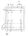
図5は、表示パネル30の構造の一部を模式的に示す、表示パネル30を裏面から見た場合の平面図である。
【0016】
この表示パネル30は、ガラスなどの透明な基板上に走査ライン5及びデータライン7がマトリクス状に配置されている。走査ライン5及びデータライン7の交差位置にはそれぞれ、アドレス選択用FET11、駆動用FET12、キャパシタ13及び発光部を構成する有機EL素子15が設けられている。尚、これらの回路構成は図1に示したものと同様である。
【0017】
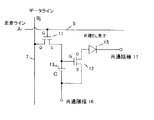
表示パネル30の裏面には、走査ライン(A1−An)に沿って延びた帯状の金属膜からなる帯状電極45(SE1−SEn)が形成されている。帯状電極45は走査ライン毎に設けられており、互いに電気的に分離されている。第k走査ライン(Ak)にFET11,12を介して接続されたEL素子15(ELk,j ,j=1〜m)の陰極は、対応する帯状電極45(SEk)に接続されている。すなわち、EL素子15の陰極は走査ライン毎に互いに電気的に分離され、走査ライン毎に独立して制御することができるようになっている。一方、EL素子15の陽極は駆動FET12を介してアノードライン47に接続されている。各アノードライン47は互いに電気的に接続されて表示パネル30内のEL素子15の共通の陽極として機能し、電源回路36の正の電圧出力端VDに接続されている。
【0018】
図6は、本実施例における表示パネル30及び帯状電極制御ドライバ35を模式的に示している。各帯状電極45は帯状電極制御ドライバ35内に設けられたスイッチS1〜Snにより選択的に電源回路36の電圧出力端VG、VB、又はVD(又はオープン)に接続されるようになっている。ここで、電圧VGは、EL素子15を発光せしめる場合に接続される電圧である。すなわち、電圧VGはアノードライン47に印加される電圧VDとの電圧差(=VD−VG)がEL素子15の所定の駆動電圧となるように選べばよい。また、EL素子15を非発光とする場合、アノードライン47は電圧VD(又はオープン)に切り換えられる。尚、この電圧は必ずしもVDでなくともよく、EL素子15を非発光とする電圧であればよい。更に、電圧VBはEL素子15に上記した逆バイアス電圧を印加するための電圧であり、アノードライン47に印加される電圧VDとの電圧差(=VD−VB<0)が所定の逆バイアス電圧となるように選ばれる。帯状電極制御ドライバ35は、表示制御部26からの制御信号に基づいて各帯状電極45に印加する電圧の切替えを行う。
【0019】
本発明における有機EL表示装置20は、このように構成され、入力映像信号に対し、各サブフィールド毎に表示パネルの画面全体のアドレス走査による発光制御を繰り返すことにより、フレーム単位の発光表示を多階調表示によって行うことができる。
以下に、表示制御部26が、表示パネル30の発光・非発光を制御して多階調表示を実現する発光制御動作について、図7に示すタイムチャートを参照しつつ詳細に説明する。
【0020】
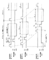
先ず、表示制御部26は、列アドレスカウンタ22、行アドレスカウンタ23、フレームメモリ24、及びマルチプレクサ25を制御し、1フレーム分のデジタル映像信号データを各サブフィールドに対応する階調表示データに変換し、マルチプレクサ25に供給する。次に、第1サブフィールド(SF1)に関する表示データのうち、第1走査ラインに対応する表示データをデータドライバ28内のデータラッチ回路(図示しない)にラッチさせる。表示制御部26はラッチされた第1走査ラインの列データのそれぞれを、対応する各アドレスに書き込む。すなわち、走査ドライバ27からアドレス信号を送出して第1走査ラインの各アドレス選択用FET11を導通せしめる。これと同時に、表示制御部26は帯状電極制御ドライバ35のスイッチS1を開状態(OPEN)からVGに切替える。これにより、第1走査ラインに対応する帯状電極45は電圧VGに接続され、映像信号データに応じて第1走査ライン内の発光すべきEL素子15は発光する。すなわち、発光を示すデータが供給されるアドレスのEL素子15を発光せしめる。
【0021】
表示制御部26は、発光開始後、所定の期間(T0)が経過したときに帯状電極制御ドライバ35を制御してスイッチS1をVGからVBに切替えて、所定の逆バイアス期間(TB)の間、帯状電極45を逆バイアス電圧に保持する。所定逆バイアス期間経過の後、スイッチS1をVBからVGに切替えて、再度EL素子15を発光せしめる。発光開始から所定の発光期間(TL,1)が経過の後、スイッチS1をVGから開状態(OPEN)に切替えて、EL素子15の発光を停止せしめる。尚、この場合、実際にEL素子15が発光している期間は、所定の発光期間から所定の逆バイアス期間を減じた期間(=TL,1−Tb)である。
【0022】
表示制御部26は、第1走査ラインの列データがラッチされた後のステップとして、上記した第1走査ラインの場合と同様にして第2走査ラインの各EL素子15の発光及び逆バイアス印加に関する制御動作を実行する。
全ての走査ライン、すなわち第n走査ラインまでの制御動作が終了した後、表示制御部26は、第2サブフィールド(SF2)に関する制御を実行する。第2サブフィールドにおいては第1サブフィールドと同様の発光制御がなされるが、帯状電極45への逆バイアス電圧印加はなされない。第3〜第nサブフィールド(SF3−SFn)については、第2サブフィールドと同様に、逆バイアス電圧を印加しない発光制御がなされる。すなわち、本実施例においては、1フレーム期間に対して、1つのサブフィールド期間においてのみ逆バイアス電圧印加が行われる。尚、本実施例において、各サブフィールド(SFk)内の各走査ラインの発光期間は同一(=TL,k )であるように制御される。
【0023】
本発明によれば、上記したように逆バイアス電圧印加制御が実行されるので、逆バイアス電圧を印加するタイミング及び印加期間の長さを走査ライン毎に任意に設定できる。一方、例えば各走査ラインに共通の電極を用いた場合では、図8に示すように、各走査ラインに同時に逆バイアス電圧が印加される。この場合、アドレス信号のパルス幅である書込み期間と逆バイアス電圧期間の相対的なタイミングに応じて各走査ラインの発光状態は変化し、走査ライン毎に輝度が異なってしまう。図9(a)に示すように、書込み期間と逆バイアス電圧期間が離れている場合と、図9(b)、(c)に示すように、これらの期間が重なっている場合とでは輝度に違いが生じる。この発光状態の変化はEL素子15を充電する際の時定数に起因するものである。しかしながら、本発明によれば、このような影響が生じないように逆バイアス電圧期間を設けることができるので、各走査ラインの発光状態を同一に維持しつつ逆バイアス電圧を印加することができる。
【0024】
また、アドレス信号に基づいて発光を停止(又は開始)する場合には、全ての走査ラインの走査が終了するまでEL素子15の発光データを更新できないので、発光期間をアドレス期間(TA)よりも短くすることができない。従って、階調表示の精度が制限されるという不都合が生じる。しかしながら、本発明によれば、前述のように、EL素子15の発光の開始及び停止のタイミングを任意に設定できるので、全ての走査ラインを走査するために要する期間であるアドレス期間(TA)よりも短い任意の発光期間をサブフィールドに対し割り当てることが可能であり、高精度の多階調表示が可能である。
【0025】
更に、本発明によれば、EL素子15の発光期間を任意に設定でき、その期間の長さによって輝度調整ができるので、例えば、駆動TFTへの輝度制御信号の振幅変調による輝度調整の場合と異なり、S/N比の劣化を生じさせることなく表示パネルの輝度を調整することが可能である。
上記した実施例においては、アドレス信号と同時にEL素子15の発光を開始するように帯状電極制御ドライバ35のスイッチを制御する場合を例に説明したが、前述のように発光の開始及び停止は任意に設定することができる。
【0026】
更に、1フレーム期間内の1つのサブフィールド期間においてのみ逆バイアス電圧を印加する場合を例に説明したが、これに限らず適宜逆バイアス電圧を印加するようにしてもよい。例えば、逆バイアス電圧の印加は数フレーム毎に1回でもよい。また、フレーム期間内における逆バイアス電圧の印加タイミングは任意でよい。
【0027】
図10は、発光期間及び逆バイアス電圧印加タイミングの他の例を示すタイムチャートである。発光期間はサブフィールド期間内の所定のタイミングに設けられ、逆バイアス印加が行われるサブフィールドにおいては、逆バイアス印加期間は発光期間と重ならないように非発光期間内に設けられている。
図11は、本発明の第2の実施例であるアクティブマトリクス型表示パネル30の構成を模式的に示している。有機EL表示装置20の構成は第1の実施例の場合と同様である。
【0028】
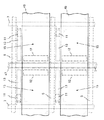
本実施例が上記した実施例と異なるのは、表示パネル30の帯状電極45が、各々が少なくとも1つの走査ラインを含む走査ラインブロック(SLB1−SLBp)毎に設けられている点である。すなわち、図11に示すように、例えば、走査ラインブロック1(SLB1)に含まれる走査ライン(A1−Ai)上のEL素子15(ELq,r ,(q=1〜i,r=1〜m))の陰極は同じ帯状電極45(SE1)に接続されている。他の各走査ラインブロック(SLB2〜SLBp)のEL素子15も同様にして帯状電極45(SE2〜SEp)の各々に接続されている。すなわち、EL素子15の陰極は走査ラインブロック毎に互いに電気的に分離されている。
【0029】
また、帯状電極制御ドライバ35は表示制御部26からの制御信号に応答して各スイッチS1〜Spを切替え、各帯状電極45を選択的に電源回路36の電圧出力端VB、VD又は接地電圧(GND)に接続する。すなわち、EL素子15を発光せしめる場合には接地電圧(GND)に、発光を停止する場合には共通陽極と同電圧のVDに、逆バイアス電圧を印加する場合には逆バイアス電圧VBに帯状電極45を接続する。このように、走査ラインブロック毎に独立して帯状電極45の接続を制御することができるようになっている。
【0030】
図12は、表示制御部26が実行する表示パネル30の制御動作を示すタイムチャートである。走査ラインブロック毎にEL素子15の発光制御及び逆バイアス電圧印加制御を行う点において、走査ライン毎に制御を行う第1の実施例の場合と異なる。各走査ラインブロックにおいて、発光制御及び逆バイアス電圧印加は、同一の走査ラインブロックに含まれる走査ラインに対して同時に行われる。また、各サブフィールドにおける発光期間の長さは同一のサブフィールド(SFk)内においては全ての走査ラインブロックに対して一定(TL,k )であるように制御される。
【0031】
図13は、本発明の第3の実施例であるアクティブマトリクス型表示パネル30の構成を模式的に示している。有機EL表示装置20の構成は第1の実施例の場合と同様である。
本実施例が上記した実施例と異なるのは、表示パネル30の帯状電極45(SE1−SEm)がデータライン(B1−Bm)に沿って形成されている点である。帯状電極45はデータライン毎に設けられており、互いに電気的に分離されている。第kデータライン(Bk)上のEL素子15(ELj,k , j=1〜n)の陰極は、対応する帯状電極45(SEk)に接続されている。各帯状電極45の電圧は帯状電極制御ドライバ35内に設けられたスイッチにより選択的に切替えることが可能である。すなわち、表示パネル30のEL素子15はデータライン毎に独立して制御することができるようになっている。従って、EL素子15に関して自由度の高い制御が可能である。
【0032】
例えば、各走査ラインに赤、緑及び青で発光する3種類のEL素子15が順に繰り返し接続されたカラー表示パネル30に本発明を適用することができる。この場合、帯状電極45の1つには1種類の発光色のEL素子15が接続されている。図12に示すように、EL素子15を発光させる場合、各帯状電極45は当該帯状電極45に接続されたEL素子15の種類に応じて、電源回路36の3種類の出力電圧(V1,V2,V3)のうち所定の1つに接続される。従って、EL素子15の種類に応じて、EL素子15の発光時の印加電圧を最適な電圧にすることができる。
【0033】
図14は、上記したカラー表示パネル30において発光時に電圧V1に接続される帯状電極45に関する制御動作を示すタイムチャートである。各走査ラインにおいてEL素子15は同時に発光し、また逆バイアス電圧印加も同時に行われる。電圧V2,V3に接続される帯状電極45も同様に制御される。また、印加電圧のみならず、発光期間をEL素子15の種類に応じて変化させてもよい。
【0034】
尚、上記した実施例においては、陰極を電気的に分離して帯状電極とした場合を例に説明したが、陽極を同様に帯状電極としてもよい。
更に、上記した実施例は例示であって、適宜組み合わせて用いることができる。
上記したように、本発明によれば、互いに電気的に分離された帯状の電極を少なくとも1つの走査ライン又はデータライン毎に設けているので、発光素子に印加する電圧及び印加のタイミングを自由に制御でき、安定性が高く高精度の多階調表示が可能である。
【0035】
【発明の効果】
上記したことから明らかなように、本発明によれば、安定性が高く高精度の多階調表示が可能なアクティブマトリクス型の表示装置を実現できる。
【図面の簡単な説明】
【図1】従来のアクティブマトリクス型表示パネルの1つの画素に対応する回路構成の1例を概略的に示す図である。
【図2】従来のアクティブマトリクス型表示パネルの概略的構成及び共通陽極及び共通陰極の接続を模式的に示す図である。
【図3】本発明の第1の実施例であるアクティブマトリクス型表示パネルを用いた有機EL表示装置の構成を概略的に示す図である。
【図4】デジタル映像信号の1フレーム期間、サブフィールド期間、及びアドレス期間を示す図である。
【図5】本発明の第1の実施例である表示パネルの構造の一部を模式的に示す平面図である。
【図6】本発明の第1の実施例である表示パネル及び帯状電極制御ドライバを模式的に示す図である。
【図7】表示制御部が実行する表示パネルの発光制御及び逆バイアス印加動作を示すタイムチャートである。
【図8】各走査ラインに同時に逆バイアス電圧を印加した場合のサブフィールド期間と逆バイアス期間の関係を模式的に示す図である。
【図9】図8における書込み期間と逆バイアス電圧期間の相対的なタイミングに応じて各走査ラインの発光状態が変化することを示す図である。
【図10】本発明の第1の実施例である表示パネルにおける、発光期間及び逆バイアス電圧印加タイミングの他の例を示すタイムチャートである。
【図11】本発明の第2の実施例であるアクティブマトリクス型表示パネルの構成を模式的に示す図である。
【図12】図11に示す表示パネルに関し表示制御部が実行する制御動作を示すタイムチャートである。
【図13】本発明の第2の実施例であるアクティブマトリクス型表示パネルの構成を模式的に示す図である。
【図14】図13に示す表示パネルに関し表示制御部が実行する制御動作を示すタイムチャートである。
【主要部分の符号の説明】
10 画素
11 アドレス選択用FET
12 駆動用FET
13 キャパシタ
15 発光素子
20 表示装置
21 A/D変換器
22 列アドレスカウンタ
23 行アドレスカウンタ
24 フレームメモリ
25 マルチプレクサ
26 表示制御部
27 走査ドライバ
28 データドライバ
30 表示パネル
35 帯状電極制御ドライバ
36 電源
45 帯状電極[0001]
BACKGROUND OF THE INVENTION
The present invention relates to an active matrix display device, and more particularly to a display device using an active matrix display panel having a light emitting element such as an organic electroluminescence element.
[0002]
[Prior art]
Development of a matrix type display using a light emitting display panel in which light emitting elements are arranged in a matrix is being widely promoted. As a light emitting element used for such a display panel, for example, there is an electroluminescent element using an organic material as a light emitting layer (hereinafter referred to as an organic EL element). In such an organic EL element, the light emission luminance can be controlled by a current flowing through the element. As a display panel using organic EL elements, a simple matrix type display panel in which organic EL elements are simply arranged in a matrix form, and an active matrix type display in which driving elements composed of transistors are added to each of the organic EL elements arranged in a matrix form There is a panel. An active matrix display panel has advantages such as low power consumption and less crosstalk between pixels compared to a simple matrix display panel, and is particularly suitable for large screen displays and high definition displays.
[0003]
FIG. 1 shows an example of a circuit configuration corresponding to one
In FIG. 1, a gate G of an FET (Field Effect Transistor) 11 (address selection transistor) is connected to an address scanning electrode line (scanning line) to which an address signal is supplied, and a source S of the
[0004]
As shown in FIG. 2, the
The light emission control operation of this circuit will be described. First, when an on-voltage is supplied to the gate G of the
[0005]
A circuit corresponding to one pixel of a display panel that performs light emission control by active matrix driving is configured in this manner, and light emission of the pixel is maintained when the
As described above, in the active matrix display panel, light emission control of each light emitting element is performed by controlling a driving circuit including a driving element such as an FET.
[0006]
[Problems to be solved by the invention]
However, the conventional active matrix display device has a problem in that the light emitting element control is low because the light emission control of each light emitting element is performed only by the drive circuit.
The present invention has been made in view of the above points, and an object thereof is to provide an active matrix display device having a high degree of freedom in controlling light emitting elements.
[0007]
[Means for Solving the Problems]
A display device according to the present invention includes a plurality of light emitting elements arranged at intersections of scanning lines and data lines arranged in a matrix, a driving circuit for driving each of the plurality of light emitting elements, and one of each of the plurality of light emitting elements. A display panel including a conductive portion connected to the terminal, a display control portion that controls a drive circuit in accordance with an input video signal, and a power supply portion that includes a power supply circuit that supplies power to the plurality of light emitting elements through the conductive portion, The conductive portion is composed of a plurality of strip-like electrodes provided for at least one of the scanning lines or the data lines and electrically separated from each other, and a plurality of power supply portions are provided. And a switch circuit for selectively connecting each of the strip electrodes to the power supply circuit.
[0008]
In addition, the display device according to the present invention reverses to the plurality of light emitting elements via the reverse bias voltage generation circuit that generates a reverse bias voltage in the direction opposite to the voltage applied when the light emitting element emits light, and the plurality of strip electrodes. And a reverse bias voltage applying circuit for selectively applying the bias voltage.
As another feature of the present invention, the display control unit includes a timer, and controls the switch circuit according to the output of the timer to selectively connect each of the plurality of strip electrodes to the power supply circuit.
[0009]
A display panel according to the present invention includes a plurality of light emitting elements arranged at intersections of scanning lines and data lines arranged in a matrix, a drive circuit that drives each of the plurality of light emitting elements, and each of the plurality of light emitting elements. A display panel including a conductive portion connected to one of the terminals, wherein the conductive portion includes a plurality of strip-like electrodes that are provided at least for each of the scanning lines or the data lines and are electrically separated from each other. It is characterized by that.
[0010]
DETAILED DESCRIPTION OF THE INVENTION
Embodiments of the present invention will be described in detail with reference to the drawings. In the drawings described below, substantially the same parts are denoted by the same reference numerals.
FIG. 3 schematically shows a configuration of an organic
[0011]
In FIG. 3, an analog / digital (A / D) converter 21 receives an analog video signal and converts it into digital video signal data. The digital video signal obtained by the conversion is supplied from the A / D converter 21 to the
On the other hand, the
[0012]
Further, the
The
[0013]
As shown in FIG. 4, in this embodiment, the luminance gradation is controlled by a method based on the
[0014]
The light emission control of each
[0015]
Further, in this embodiment, when there is a poorly formed portion in the organic EL light emitting layer, a reverse bias voltage is applied to the organic EL element to prevent a leakage current from occurring in that portion and causing a defective light emission. The part can be removed.
FIG. 5 is a plan view schematically showing a part of the structure of the
[0016]
In the
[0017]
On the back surface of the
[0018]
FIG. 6 schematically shows the
[0019]
The organic
Hereinafter, a light emission control operation in which the
[0020]
First, the
[0021]
The
[0022]
As a step after the column data of the first scan line is latched, the
After the control operation up to all the scan lines, that is, the nth scan line is completed, the
[0023]
According to the present invention, since the reverse bias voltage application control is executed as described above, the timing for applying the reverse bias voltage and the length of the application period can be arbitrarily set for each scanning line. On the other hand, for example, when a common electrode is used for each scanning line, a reverse bias voltage is simultaneously applied to each scanning line as shown in FIG. In this case, the light emission state of each scanning line changes according to the relative timing of the address period and the reverse bias voltage period, which is the pulse width of the address signal, and the luminance differs for each scanning line. As shown in FIG. 9 (a), when the writing period and the reverse bias voltage period are separated from each other, and when these periods overlap as shown in FIGS. 9 (b) and 9 (c), the luminance is increased. A difference is made. This change in the light emission state is caused by a time constant when the
[0024]
In addition, when light emission is stopped (or started) based on the address signal, the light emission data of the
[0025]
Furthermore, according to the present invention, the light emission period of the
In the embodiment described above, the case where the switch of the strip
[0026]
Furthermore, although the case where the reverse bias voltage is applied only in one subfield period within one frame has been described as an example, the present invention is not limited to this, and the reverse bias voltage may be applied as appropriate. For example, the reverse bias voltage may be applied once every several frames. Further, the application timing of the reverse bias voltage within the frame period may be arbitrary.
[0027]
FIG. 10 is a time chart showing another example of the light emission period and the reverse bias voltage application timing. The light emission period is provided at a predetermined timing within the subfield period. In the subfield where reverse bias application is performed, the reverse bias application period is provided within the non-light emission period so as not to overlap the light emission period.
FIG. 11 schematically shows the configuration of an active
[0028]
This embodiment is different from the above-described embodiment in that the
[0029]
The strip
[0030]
FIG. 12 is a time chart showing the control operation of the
[0031]
FIG. 13 schematically shows the configuration of an active
The present embodiment is different from the above-described embodiment in that the strip electrode 45 (SE1-SEm) of the
[0032]
For example, the present invention can be applied to a
[0033]
Figure 14 is a time chart showing the control operation with regard to the band-
[0034]
In the above-described embodiments, the case where the cathode is electrically separated to form a strip electrode has been described as an example. However, the anode may be similarly formed as a strip electrode.
Furthermore, the above-described embodiments are examples and can be used in appropriate combinations.
As described above, according to the present invention, the strip-like electrodes that are electrically separated from each other are provided for at least one scanning line or data line, so that the voltage applied to the light emitting element and the timing of application can be freely set. Controllable, highly stable and highly accurate multi-gradation display is possible.
[0035]
【The invention's effect】
As is apparent from the above, according to the present invention, an active matrix display device capable of high-precision multi-gradation display with high stability can be realized.
[Brief description of the drawings]
FIG. 1 is a diagram schematically showing an example of a circuit configuration corresponding to one pixel of a conventional active matrix display panel.
FIG. 2 is a diagram schematically showing a schematic configuration of a conventional active matrix display panel and a connection between a common anode and a common cathode.
FIG. 3 is a diagram schematically showing a configuration of an organic EL display device using an active matrix display panel according to a first embodiment of the present invention.
FIG. 4 is a diagram illustrating one frame period, a subfield period, and an address period of a digital video signal.
FIG. 5 is a plan view schematically showing a part of the structure of the display panel according to the first embodiment of the present invention.
FIG. 6 is a diagram schematically showing a display panel and a strip electrode control driver according to the first embodiment of the present invention.
FIG. 7 is a time chart showing light emission control and reverse bias application operation of the display panel executed by the display control unit.
FIG. 8 is a diagram schematically showing a relationship between a subfield period and a reverse bias period when a reverse bias voltage is simultaneously applied to each scanning line.
FIG. 9 is a diagram showing that the light emission state of each scanning line changes according to the relative timing of the writing period and the reverse bias voltage period in FIG.
FIG. 10 is a time chart showing another example of the light emission period and the reverse bias voltage application timing in the display panel according to the first embodiment of the present invention.
FIG. 11 is a diagram schematically showing a configuration of an active matrix display panel according to a second embodiment of the present invention.
12 is a time chart showing a control operation performed by the display control unit with respect to the display panel shown in FIG.
FIG. 13 is a diagram schematically showing a configuration of an active matrix display panel according to a second embodiment of the present invention.
14 is a time chart showing a control operation executed by a display control unit with respect to the display panel shown in FIG.
[Explanation of main part codes]
10
12 Driving FET
13
Claims (5)
前記発光素子の発光時に印加される電圧とは逆方向の逆バイアス電圧を生成する逆バイアス電圧生成回路と、
逆バイアス電圧印加回路と、を有し、
前記導電部は、前記走査線の少なくとも1つ毎に設けられて互いに電気的に分離された複数の帯状電極からなり、前記電源部は前記複数の帯状電極の各々を前記電源回路に選択的に接続するスイッチ回路を含み、
前記逆バイアス電圧印加回路は、前記複数の帯状電極を介して前記複数の発光素子に前記逆バイアス電圧を選択的に印加することを特徴とする表示装置。Connected to a plurality of light emitting elements arranged at intersections of scanning lines and data lines arranged in a matrix, a drive circuit for driving each of the plurality of light emitting elements, and one terminal of each of the plurality of light emitting elements. A display panel including a conductive portion; a display control portion that controls the drive circuit in accordance with an input video signal; and a power supply portion including a power supply circuit that supplies power to the plurality of light emitting elements via the conductive portion. An active matrix display device comprising:
A reverse bias voltage generation circuit for generating a reverse bias voltage in a direction opposite to a voltage applied when the light emitting element emits light;
A reverse bias voltage application circuit,
The conductive portion includes a plurality of strip-like electrodes provided for at least one of the scanning lines and electrically separated from each other, and the power supply portion selectively selects each of the plurality of strip-like electrodes for the power supply circuit. look including a switch circuit to be connected,
The display device, wherein the reverse bias voltage application circuit selectively applies the reverse bias voltage to the plurality of light emitting elements through the plurality of strip electrodes .
前記発光素子の発光時に印加される電圧とは逆方向の逆バイアス電圧を生成する逆バイアス電圧生成回路と、
逆バイアス電圧印加回路と、を有し、
前記導電部は、前記データ線の少なくとも1つ毎に設けられて互いに電気的に分離された複数の帯状電極からなり、前記電源部は前記複数の帯状電極の各々を前記電源回路に選択的に接続するスイッチ回路を含み、
前記逆バイアス電圧印加回路は、前記複数の帯状電極を介して前記複数の発光素子に前記逆バイアス電圧を選択的に印加することを特徴とする表示装置。Connected to a plurality of light emitting elements arranged at intersections of scanning lines and data lines arranged in a matrix, a drive circuit for driving each of the plurality of light emitting elements, and one terminal of each of the plurality of light emitting elements. A display panel including a conductive portion; a display control portion that controls the drive circuit in accordance with an input video signal; and a power supply portion including a power supply circuit that supplies power to the plurality of light emitting elements via the conductive portion. An active matrix display device comprising:
A reverse bias voltage generation circuit for generating a reverse bias voltage in a direction opposite to a voltage applied when the light emitting element emits light;
A reverse bias voltage application circuit,
The conductive portion includes a plurality of strip-shaped electrodes provided for at least one of the data lines and electrically separated from each other, and the power supply section selectively selects each of the plurality of strip-shaped electrodes for the power supply circuit. look including a switch circuit to be connected,
The display device, wherein the reverse bias voltage application circuit selectively applies the reverse bias voltage to the plurality of light emitting elements through the plurality of strip electrodes .
前記発光素子の発光時に印加される電圧とは逆方向の逆バイアス電圧を生成する逆バイアス電圧生成回路と、 A reverse bias voltage generation circuit for generating a reverse bias voltage in a direction opposite to a voltage applied when the light emitting element emits light;
前記逆バイアス電圧を印加する逆バイアス電圧印加回路と、A reverse bias voltage application circuit for applying the reverse bias voltage;
タイマと、を有し、A timer, and
前記導電部は、前記走査線の少なくとも1つ毎に設けられて互いに電気的に分離された複数の帯状電極からなり、前記電源部は前記複数の帯状電極の各々を前記電源回路に選択的に接続するスイッチ回路を含み、The conductive portion includes a plurality of strip-like electrodes provided for at least one of the scanning lines and electrically separated from each other, and the power supply portion selectively selects each of the plurality of strip-like electrodes for the power supply circuit. Including switch circuit to connect,
前記逆バイアス電圧印加回路は、前記タイマの出力に応じて前記複数の帯状電極を介して前記複数の発光素子に前記逆バイアス電圧を選択的に印加することを特徴とする表示装置。The display device, wherein the reverse bias voltage application circuit selectively applies the reverse bias voltage to the plurality of light emitting elements via the plurality of strip electrodes in accordance with an output of the timer.
前記発光素子の発光時に印加される電圧とは逆方向の逆バイアス電圧を生成する逆バイアス電圧生成回路と、
前記逆バイアス電圧を印加する逆バイアス電圧印加回路と、
タイマと、を有し、
前記導電部は、前記データ線の少なくとも1つ毎に設けられて互いに電気的に分離された複数の帯状電極からなり、前記電源部は前記複数の帯状電極の各々を前記電源回路に選択的に接続するスイッチ回路を含み、
前記逆バイアス電圧印加回路は、前記タイマの出力に応じて前記複数の帯状電極を介して前記複数の発光素子に前記逆バイアス電圧を選択的に印加することを特徴とする表示装置。 Connected to a plurality of light emitting elements arranged at intersections of scanning lines and data lines arranged in a matrix, a drive circuit for driving each of the plurality of light emitting elements, and one terminal of each of the plurality of light emitting elements. A display panel including a conductive portion; a display control portion that controls the drive circuit in accordance with an input video signal; and a power supply portion including a power supply circuit that supplies power to the plurality of light emitting elements via the conductive portion. An active matrix display device comprising:
A reverse bias voltage generation circuit for generating a reverse bias voltage in a direction opposite to a voltage applied when the light emitting element emits light;
A reverse bias voltage application circuit for applying the reverse bias voltage;
A timer, and
The conductive portion includes a plurality of strip-shaped electrodes provided for at least one of the data lines and electrically separated from each other, and the power supply section selectively selects each of the plurality of strip-shaped electrodes for the power supply circuit. Including switch circuit to connect,
The display device, wherein the reverse bias voltage application circuit selectively applies the reverse bias voltage to the plurality of light emitting elements through the plurality of strip electrodes in accordance with an output of the timer .
Priority Applications (2)
| Application Number | Priority Date | Filing Date | Title |
|---|---|---|---|
| JP32272699A JP3594856B2 (en) | 1999-11-12 | 1999-11-12 | Active matrix display device |
| US09/708,855 US6731276B1 (en) | 1999-11-12 | 2000-11-09 | Active matrix light-emitting display apparatus |
Applications Claiming Priority (1)
| Application Number | Priority Date | Filing Date | Title |
|---|---|---|---|
| JP32272699A JP3594856B2 (en) | 1999-11-12 | 1999-11-12 | Active matrix display device |
Related Child Applications (1)
| Application Number | Title | Priority Date | Filing Date |
|---|---|---|---|
| JP2004144540A Division JP3862271B2 (en) | 2004-05-14 | 2004-05-14 | Active matrix display device |
Publications (3)
| Publication Number | Publication Date |
|---|---|
| JP2001142413A JP2001142413A (en) | 2001-05-25 |
| JP2001142413A5 JP2001142413A5 (en) | 2004-12-02 |
| JP3594856B2 true JP3594856B2 (en) | 2004-12-02 |
Family
ID=18146945
Family Applications (1)
| Application Number | Title | Priority Date | Filing Date |
|---|---|---|---|
| JP32272699A Expired - Lifetime JP3594856B2 (en) | 1999-11-12 | 1999-11-12 | Active matrix display device |
Country Status (2)
| Country | Link |
|---|---|
| US (1) | US6731276B1 (en) |
| JP (1) | JP3594856B2 (en) |
Families Citing this family (47)
| Publication number | Priority date | Publication date | Assignee | Title |
|---|---|---|---|---|
| TW591584B (en) | 1999-10-21 | 2004-06-11 | Semiconductor Energy Lab | Active matrix type display device |
| US6909111B2 (en) * | 2000-12-28 | 2005-06-21 | Semiconductor Energy Laboratory Co., Ltd. | Method of manufacturing a light emitting device and thin film forming apparatus |
| JP3757797B2 (en) * | 2001-01-09 | 2006-03-22 | 株式会社日立製作所 | Organic LED display and driving method thereof |
| JP3593982B2 (en) * | 2001-01-15 | 2004-11-24 | ソニー株式会社 | Active matrix type display device, active matrix type organic electroluminescence display device, and driving method thereof |
| JP4869497B2 (en) | 2001-05-30 | 2012-02-08 | 株式会社半導体エネルギー研究所 | Display device |
| US7227517B2 (en) * | 2001-08-23 | 2007-06-05 | Seiko Epson Corporation | Electronic device driving method, electronic device, semiconductor integrated circuit, and electronic apparatus |
| JP4873677B2 (en) * | 2001-09-06 | 2012-02-08 | 東北パイオニア株式会社 | Driving device for light emitting display panel |
| JP2006338042A (en) * | 2001-09-21 | 2006-12-14 | Semiconductor Energy Lab Co Ltd | Light emitting device, and driving method of light emitting device |
| JP3810725B2 (en) | 2001-09-21 | 2006-08-16 | 株式会社半導体エネルギー研究所 | LIGHT EMITTING DEVICE AND ELECTRONIC DEVICE |
| TW574529B (en) * | 2001-09-28 | 2004-02-01 | Tokyo Shibaura Electric Co | Organic electro-luminescence display device |
| GB0130176D0 (en) * | 2001-12-18 | 2002-02-06 | Koninkl Philips Electronics Nv | Electroluminescent display device |
| US7042162B2 (en) | 2002-02-28 | 2006-05-09 | Semiconductor Energy Laboratory Co., Ltd. | Light emitting device |
| JP4024557B2 (en) | 2002-02-28 | 2007-12-19 | 株式会社半導体エネルギー研究所 | Light emitting device, electronic equipment |
| US7330162B2 (en) * | 2002-02-28 | 2008-02-12 | Semiconductor Energy Laboratory Co., Ltd. | Method of driving a light emitting device and electronic equipment |
| JP2003323157A (en) * | 2002-02-28 | 2003-11-14 | Semiconductor Energy Lab Co Ltd | Driving method of light emitting device and electronic equipment |
| US7023141B2 (en) | 2002-03-01 | 2006-04-04 | Semiconductor Energy Laboratory Co., Ltd. | Light emitting device and drive method thereof |
| JP2003302936A (en) * | 2002-03-29 | 2003-10-24 | Internatl Business Mach Corp <Ibm> | Display device, oled panel, device and method for controlling thin film transistor, and method for controlling oled display |
| KR20040019207A (en) * | 2002-08-27 | 2004-03-05 | 엘지.필립스 엘시디 주식회사 | Organic electro-luminescence device and apparatus and method driving the same |
| JP2004109718A (en) * | 2002-09-20 | 2004-04-08 | Hitachi Ltd | Image display device |
| JP2006072385A (en) * | 2002-10-03 | 2006-03-16 | Seiko Epson Corp | Electronic device and electronic equipment |
| JP2004145300A (en) | 2002-10-03 | 2004-05-20 | Seiko Epson Corp | Electronic circuit, method for driving electronic circuit, electronic device, electrooptical device, method for driving electrooptical device, and electronic apparatus |
| US7256758B2 (en) * | 2003-06-02 | 2007-08-14 | Au Optronics Corporation | Apparatus and method of AC driving OLED |
| JP4511128B2 (en) * | 2003-06-05 | 2010-07-28 | 奇美電子股▲ふん▼有限公司 | Active matrix image display device |
| US8937580B2 (en) * | 2003-08-08 | 2015-01-20 | Semiconductor Energy Laboratory Co., Ltd. | Driving method of light emitting device and light emitting device |
| CN101488322B (en) * | 2003-08-29 | 2012-06-20 | 精工爱普生株式会社 | Electro-optical device, method of driving the same, and electronic apparatus |
| JP3987824B2 (en) * | 2003-09-12 | 2007-10-10 | 勝華科技股▲ふん▼有限公司 | Driving circuit and driving method for active matrix organic EL display |
| JP2005128361A (en) * | 2003-10-27 | 2005-05-19 | Tohoku Pioneer Corp | Driving device and driving method for spontaneous light emitting display panel |
| GB0400209D0 (en) * | 2004-01-07 | 2004-02-11 | Koninkl Philips Electronics Nv | Light emitting display devices |
| KR101080350B1 (en) * | 2004-04-07 | 2011-11-04 | 삼성전자주식회사 | Display device and method of driving thereof |
| KR20050115346A (en) * | 2004-06-02 | 2005-12-07 | 삼성전자주식회사 | Display device and driving method thereof |
| US7592975B2 (en) | 2004-08-27 | 2009-09-22 | Semiconductor Energy Laboratory Co., Ltd. | Display device and driving method thereof |
| TWI648719B (en) | 2004-09-16 | 2019-01-21 | 日商半導體能源研究所股份有限公司 | Display device and electronic device with pixels |
| KR20060096857A (en) * | 2005-03-04 | 2006-09-13 | 삼성전자주식회사 | Display device and driving method thereof |
| CN100405443C (en) * | 2005-04-22 | 2008-07-23 | 中国科学院长春光学精密机械与物理研究所 | Method for improving a-Si-TFT organic electro LED lightness stability |
| TWI328213B (en) * | 2005-12-16 | 2010-08-01 | Chi Mei El Corp | Plate display and pixel circuitry |
| KR101282399B1 (en) * | 2006-04-04 | 2013-07-04 | 삼성디스플레이 주식회사 | Display device and driving method thereof |
| CN101192372B (en) * | 2006-11-28 | 2012-07-04 | 奇美电子股份有限公司 | Display panel and its structure |
| JP4760840B2 (en) * | 2008-02-28 | 2011-08-31 | ソニー株式会社 | EL display panel, electronic device, and driving method of EL display panel |
| JP2009258301A (en) * | 2008-04-15 | 2009-11-05 | Eastman Kodak Co | Display device |
| WO2010146707A1 (en) * | 2009-06-19 | 2010-12-23 | パイオニア株式会社 | Active matrix type organic el display device and method for driving the same |
| KR20110013693A (en) * | 2009-08-03 | 2011-02-10 | 삼성모바일디스플레이주식회사 | Organic light emitting display and driving method thereof |
| KR101056281B1 (en) | 2009-08-03 | 2011-08-11 | 삼성모바일디스플레이주식회사 | Organic electroluminescent display and driving method thereof |
| KR101152464B1 (en) * | 2010-05-10 | 2012-06-01 | 삼성모바일디스플레이주식회사 | Organic Light Emitting Display Device and Driving Method Thereof |
| KR101645404B1 (en) | 2010-07-06 | 2016-08-04 | 삼성디스플레이 주식회사 | Organic Light Emitting Display |
| US20150161934A1 (en) * | 2013-12-06 | 2015-06-11 | Shenzhen China Star Optoelectronics Technology Co. Ltd. | Driving circuit and driving method of display |
| CN108154849B (en) * | 2016-11-28 | 2020-12-01 | 伊格尼斯创新公司 | Pixel, reference circuit and timing technique |
| KR20220089197A (en) * | 2020-12-21 | 2022-06-28 | 엘지디스플레이 주식회사 | Infinitely Expandable Display Device |
Family Cites Families (4)
| Publication number | Priority date | Publication date | Assignee | Title |
|---|---|---|---|---|
| US5552678A (en) * | 1994-09-23 | 1996-09-03 | Eastman Kodak Company | AC drive scheme for organic led |
| TW441136B (en) * | 1997-01-28 | 2001-06-16 | Casio Computer Co Ltd | An electroluminescent display device and a driving method thereof |
| TW540251B (en) * | 1999-09-24 | 2003-07-01 | Semiconductor Energy Lab | EL display device and method for driving the same |
| JP2001109432A (en) * | 1999-10-06 | 2001-04-20 | Pioneer Electronic Corp | Driving device for active matrix type light emitting panel |
-
1999
- 1999-11-12 JP JP32272699A patent/JP3594856B2/en not_active Expired - Lifetime
-
2000
- 2000-11-09 US US09/708,855 patent/US6731276B1/en not_active Expired - Fee Related
Also Published As
| Publication number | Publication date |
|---|---|
| JP2001142413A (en) | 2001-05-25 |
| US6731276B1 (en) | 2004-05-04 |
Similar Documents
| Publication | Publication Date | Title |
|---|---|---|
| JP3594856B2 (en) | Active matrix display device | |
| JP3973471B2 (en) | Digital drive display device | |
| EP1094438A1 (en) | Active matrix display apparatus and driving method therefor | |
| US7609234B2 (en) | Pixel circuit and driving method for active matrix organic light-emitting diodes, and display using the same | |
| US7379044B2 (en) | Image display apparatus | |
| US8063858B2 (en) | Active matrix display apparatus and driving method therefor | |
| JP2001109432A (en) | Driving device for active matrix type light emitting panel | |
| JP2000235370A (en) | Drive assembly for organic electroluminescent element | |
| KR20050043818A (en) | Display device employing current-driven type light-emitting elements and method of driving same | |
| JP2001042822A (en) | Active matrix type display device | |
| JPH10312173A (en) | Picture display device | |
| JP2000347622A (en) | Display device and its driving method | |
| KR100530559B1 (en) | Display driving circuit | |
| JP3953383B2 (en) | Driving device and driving method of light emitting display panel | |
| JP2004151194A (en) | Driving device for active light emitting display panel | |
| JP3712104B2 (en) | Matrix type display device and driving method thereof | |
| JP2002278497A (en) | Display panel and driving method therefor | |
| KR20040019208A (en) | Aging Circuit For Organic Electroluminescence Device And Method Of Driving The same | |
| JP5550233B2 (en) | Method for driving a display panel using depolarization | |
| JP2003043999A (en) | Display pixel circuit and self-luminous display device | |
| JP2003150108A (en) | Active matrix substrate and method for driving current controlled type light emitting element using the same | |
| JP2003195806A (en) | Light emitting circuit of organic electroluminescence element and display device | |
| KR20040062065A (en) | active matrix organic electroluminescence display device | |
| JP2005107063A (en) | Device and method for driving self-luminous display panel | |
| JP2002287664A (en) | Display panel and its driving method |
Legal Events
| Date | Code | Title | Description |
|---|---|---|---|
| A521 | Request for written amendment filed |
Free format text: JAPANESE INTERMEDIATE CODE: A523 Effective date: 20031212 |
|
| A621 | Written request for application examination |
Free format text: JAPANESE INTERMEDIATE CODE: A621 Effective date: 20031212 |
|
| A871 | Explanation of circumstances concerning accelerated examination |
Free format text: JAPANESE INTERMEDIATE CODE: A871 Effective date: 20031212 |
|
| A975 | Report on accelerated examination |
Free format text: JAPANESE INTERMEDIATE CODE: A971005 Effective date: 20040303 |
|
| A131 | Notification of reasons for refusal |
Free format text: JAPANESE INTERMEDIATE CODE: A131 Effective date: 20040315 |
|
| A521 | Request for written amendment filed |
Free format text: JAPANESE INTERMEDIATE CODE: A523 Effective date: 20040514 |
|
| TRDD | Decision of grant or rejection written | ||
| A01 | Written decision to grant a patent or to grant a registration (utility model) |
Free format text: JAPANESE INTERMEDIATE CODE: A01 Effective date: 20040831 |
|
| A61 | First payment of annual fees (during grant procedure) |
Free format text: JAPANESE INTERMEDIATE CODE: A61 Effective date: 20040901 |
|
| R150 | Certificate of patent or registration of utility model |
Ref document number: 3594856 Country of ref document: JP Free format text: JAPANESE INTERMEDIATE CODE: R150 Free format text: JAPANESE INTERMEDIATE CODE: R150 |
|
| FPAY | Renewal fee payment (event date is renewal date of database) |
Free format text: PAYMENT UNTIL: 20070910 Year of fee payment: 3 |
|
| FPAY | Renewal fee payment (event date is renewal date of database) |
Free format text: PAYMENT UNTIL: 20080910 Year of fee payment: 4 |
|
| FPAY | Renewal fee payment (event date is renewal date of database) |
Free format text: PAYMENT UNTIL: 20090910 Year of fee payment: 5 |
|
| FPAY | Renewal fee payment (event date is renewal date of database) |
Free format text: PAYMENT UNTIL: 20100910 Year of fee payment: 6 |
|
| FPAY | Renewal fee payment (event date is renewal date of database) |
Free format text: PAYMENT UNTIL: 20100910 Year of fee payment: 6 |
|
| FPAY | Renewal fee payment (event date is renewal date of database) |
Free format text: PAYMENT UNTIL: 20110910 Year of fee payment: 7 |
|
| FPAY | Renewal fee payment (event date is renewal date of database) |
Free format text: PAYMENT UNTIL: 20120910 Year of fee payment: 8 |
|
| FPAY | Renewal fee payment (event date is renewal date of database) |
Free format text: PAYMENT UNTIL: 20120910 Year of fee payment: 8 |
|
| FPAY | Renewal fee payment (event date is renewal date of database) |
Free format text: PAYMENT UNTIL: 20130910 Year of fee payment: 9 |
|
| EXPY | Cancellation because of completion of term |