JP2025041261A - 半導体装置 - Google Patents
半導体装置 Download PDFInfo
- Publication number
- JP2025041261A JP2025041261A JP2023148452A JP2023148452A JP2025041261A JP 2025041261 A JP2025041261 A JP 2025041261A JP 2023148452 A JP2023148452 A JP 2023148452A JP 2023148452 A JP2023148452 A JP 2023148452A JP 2025041261 A JP2025041261 A JP 2025041261A
- Authority
- JP
- Japan
- Prior art keywords
- trench
- electrode
- type
- semiconductor device
- layer
- Prior art date
- Legal status (The legal status is an assumption and is not a legal conclusion. Google has not performed a legal analysis and makes no representation as to the accuracy of the status listed.)
- Pending
Links
Images



Classifications
-
- H—ELECTRICITY
- H10—SEMICONDUCTOR DEVICES; ELECTRIC SOLID-STATE DEVICES NOT OTHERWISE PROVIDED FOR
- H10D—INORGANIC ELECTRIC SEMICONDUCTOR DEVICES
- H10D12/00—Bipolar devices controlled by the field effect, e.g. insulated-gate bipolar transistors [IGBT]
- H10D12/01—Manufacture or treatment
- H10D12/031—Manufacture or treatment of IGBTs
- H10D12/032—Manufacture or treatment of IGBTs of vertical IGBTs
- H10D12/038—Manufacture or treatment of IGBTs of vertical IGBTs having a recessed gate, e.g. trench-gate IGBTs
-
- H—ELECTRICITY
- H10—SEMICONDUCTOR DEVICES; ELECTRIC SOLID-STATE DEVICES NOT OTHERWISE PROVIDED FOR
- H10D—INORGANIC ELECTRIC SEMICONDUCTOR DEVICES
- H10D62/00—Semiconductor bodies, or regions thereof, of devices having potential barriers
- H10D62/10—Shapes, relative sizes or dispositions of the regions of the semiconductor bodies; Shapes of the semiconductor bodies
- H10D62/102—Constructional design considerations for preventing surface leakage or controlling electric field concentration
-
- H—ELECTRICITY
- H10—SEMICONDUCTOR DEVICES; ELECTRIC SOLID-STATE DEVICES NOT OTHERWISE PROVIDED FOR
- H10D—INORGANIC ELECTRIC SEMICONDUCTOR DEVICES
- H10D12/00—Bipolar devices controlled by the field effect, e.g. insulated-gate bipolar transistors [IGBT]
- H10D12/411—Insulated-gate bipolar transistors [IGBT]
- H10D12/441—Vertical IGBTs
- H10D12/461—Vertical IGBTs having non-planar surfaces, e.g. having trenches, recesses or pillars in the surfaces of the emitter, base or collector regions
- H10D12/481—Vertical IGBTs having non-planar surfaces, e.g. having trenches, recesses or pillars in the surfaces of the emitter, base or collector regions having gate structures on slanted surfaces, on vertical surfaces, or in grooves, e.g. trench gate IGBTs
-
- H—ELECTRICITY
- H10—SEMICONDUCTOR DEVICES; ELECTRIC SOLID-STATE DEVICES NOT OTHERWISE PROVIDED FOR
- H10D—INORGANIC ELECTRIC SEMICONDUCTOR DEVICES
- H10D64/00—Electrodes of devices having potential barriers
- H10D64/111—Field plates
- H10D64/117—Recessed field plates, e.g. trench field plates or buried field plates
-
- H—ELECTRICITY
- H10—SEMICONDUCTOR DEVICES; ELECTRIC SOLID-STATE DEVICES NOT OTHERWISE PROVIDED FOR
- H10D—INORGANIC ELECTRIC SEMICONDUCTOR DEVICES
- H10D64/00—Electrodes of devices having potential barriers
- H10D64/20—Electrodes characterised by their shapes, relative sizes or dispositions
- H10D64/27—Electrodes not carrying the current to be rectified, amplified, oscillated or switched, e.g. gates
- H10D64/311—Gate electrodes for field-effect devices
- H10D64/411—Gate electrodes for field-effect devices for FETs
- H10D64/511—Gate electrodes for field-effect devices for FETs for IGFETs
- H10D64/517—Gate electrodes for field-effect devices for FETs for IGFETs characterised by the conducting layers
- H10D64/519—Gate electrodes for field-effect devices for FETs for IGFETs characterised by the conducting layers characterised by their top-view geometrical layouts
-
- H—ELECTRICITY
- H10—SEMICONDUCTOR DEVICES; ELECTRIC SOLID-STATE DEVICES NOT OTHERWISE PROVIDED FOR
- H10D—INORGANIC ELECTRIC SEMICONDUCTOR DEVICES
- H10D12/00—Bipolar devices controlled by the field effect, e.g. insulated-gate bipolar transistors [IGBT]
- H10D12/411—Insulated-gate bipolar transistors [IGBT]
- H10D12/417—Insulated-gate bipolar transistors [IGBT] having a drift region having a doping concentration that is higher at the collector side relative to other parts of the drift region
-
- H—ELECTRICITY
- H10—SEMICONDUCTOR DEVICES; ELECTRIC SOLID-STATE DEVICES NOT OTHERWISE PROVIDED FOR
- H10D—INORGANIC ELECTRIC SEMICONDUCTOR DEVICES
- H10D12/00—Bipolar devices controlled by the field effect, e.g. insulated-gate bipolar transistors [IGBT]
- H10D12/411—Insulated-gate bipolar transistors [IGBT]
- H10D12/418—Insulated-gate bipolar transistors [IGBT] having a drift region having a doping concentration that is higher at the emitter side relative to other parts of the drift region
-
- H—ELECTRICITY
- H10—SEMICONDUCTOR DEVICES; ELECTRIC SOLID-STATE DEVICES NOT OTHERWISE PROVIDED FOR
- H10D—INORGANIC ELECTRIC SEMICONDUCTOR DEVICES
- H10D30/00—Field-effect transistors [FET]
- H10D30/60—Insulated-gate field-effect transistors [IGFET]
- H10D30/64—Double-diffused metal-oxide semiconductor [DMOS] FETs
- H10D30/66—Vertical DMOS [VDMOS] FETs
- H10D30/668—Vertical DMOS [VDMOS] FETs having trench gate electrodes, e.g. UMOS transistors
-
- H—ELECTRICITY
- H10—SEMICONDUCTOR DEVICES; ELECTRIC SOLID-STATE DEVICES NOT OTHERWISE PROVIDED FOR
- H10D—INORGANIC ELECTRIC SEMICONDUCTOR DEVICES
- H10D62/00—Semiconductor bodies, or regions thereof, of devices having potential barriers
- H10D62/10—Shapes, relative sizes or dispositions of the regions of the semiconductor bodies; Shapes of the semiconductor bodies
- H10D62/124—Shapes, relative sizes or dispositions of the regions of semiconductor bodies or of junctions between the regions
- H10D62/126—Top-view geometrical layouts of the regions or the junctions
- H10D62/127—Top-view geometrical layouts of the regions or the junctions of cellular field-effect devices, e.g. multicellular DMOS transistors or IGBTs
Landscapes
- Electrodes Of Semiconductors (AREA)
Abstract

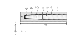
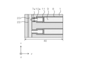
【解決手段】半導体装置の外周領域40に位置するトレンチ7の延伸方向の外周部において、下部電極10のうち上部電極9よりも外側まで延設されている下部電極の延設部10aを、前記上部電極9の端部を覆うように、前記半導体基板の上面までさらに延設し、トレンチ7の幅を、トレンチ端部7aにおいて最も狭くする。
【選択図】図3
Description
以下の説明において、n型およびp型は半導体の導電型を示し、本開示においては、第1導電型をn型、第2導電型をp型として説明するが、第1導電型をp型、第2導電型をn型としてもよい。また、n-型は不純物濃度がn型よりも低濃度であることを示し、n+型は不純物濃度がn型よりも高濃度であることを示す。同様に、p-型は不純物濃度がp型よりも低濃度であることを示し、p+型は不純物濃度がp型よりも高濃度であることを示す。
実施の形態1について図面を用いて以下に説明する。図1は、実施の形態1に係る半導体装置100全体の上面構成を模式的に示す平面図である。図1に示すように、半導体装置100には、半導体スイッチング素子が構成される活性領域30と、活性領域30の周囲に外周領域40が存在している。さらに、トレンチ7が活性領域30から外周領域40に向かって、Y方向に延伸するように設けられている。Y方向をトレンチ7の延伸方向とする。また、複数のトレンチ7が、トレンチ7の延伸方向と直行する方向であるX方向において隣り合うように設けられている。図1では、トレンチ7の数を5個で示しているが、トレンチ7の数は、これに限るものではない。また、本実施形態では、スプリットゲートのトレンチ構造を有し、半導体スイッチング素子として、絶縁ゲート型バイポーラトランジスタ(Insulated Gate Bipolar Transistor:以下、IGBTと略する)を用いる半導体装置を例に挙げて説明する。以下、図2~図5に基づいて本実施形態の半導体装置100の詳細な構造について説明する。
実施の形態2における半導体装置について図6、7を用いて説明する。図6、7は、図4、5と同様に、トレンチ7の外周部における平面図を示している。ここで、図6に示すように、トレンチ7のうち、トレンチ端部7aの幅を第1幅W1とする。また、トレンチ7のうち、トレンチ幅が最も広くなる領域のトレンチ幅を第2幅W2とする。実施の形態2の半導体装置は、実施の形態1と同様にトレンチ7が、トレンチ端部7aにおいてトレンチ幅が最も狭くなるように形成される。さらに、トレンチ端部7aのトレンチ幅は、トレンチ7のうちトレンチ幅が最も広くなる領域の幅よりも狭いことを特徴としている。つまり、トレンチ7はトレンチ幅がW1<W2となるように形成され、さらにトレンチ幅がW2からW1となるようにトレンチ端部7aの先端に向かうにつれて、トレンチ幅が徐々に狭くなっている。実施の形態2では、トレンチ幅が最も広くなる領域は、トレンチ7のうち、外周領域における上部電極9の一部に対応する領域とする。
実施の形態3における半導体装置について図8から図10を用いて説明する。図8から図10は、図4、5と同様に、トレンチ7の外周部における平面図を示している。ここで、実施の形態3の半導体装置は、実施の形態1と同様にトレンチ端部7aの幅を第1幅W1とし、トレンチ端部7aにおけるトレンチ幅が最小のW1となるように形成される。さらに、トレンチ端部7aにおいて、トレンチ端部7aの先端に向かうにつれて、トレンチ幅が徐々に狭くなることを特徴としている。
実施の形態4における半導体装置について図11を用いて説明する。図11は、図4、5と同様に、トレンチ7の外周部における平面図を示している。実施の形態4の半導体装置は、実施の形態1と同様にトレンチ端部7aの幅を第1幅W1とし、トレンチ端部7aにおけるトレンチ幅が最小のW1となるように形成される。さらに、延設部10aのそれぞれが、トレンチ7の延伸方向と交差する方向であるX方向に延伸する交差トレンチ21によって接合され、隣り合う下部電極10同士が繋がることを特徴とする。
Claims (9)
- 半導体スイッチング素子が構成されている活性領域と、前記活性領域の外側のゲート電極が設けられている外周領域が存在する半導体装置であって、
前記半導体スイッチング素子は、
第1導電型ドリフト層と、
前記第1導電型ドリフト層の上面側に設けられた第2導電型ベース層と、
前記第2導電型ベース層の上面側に設けられた第1導電型ソース層と、
前記第1導電型ドリフト層の下面側に設けられた第2導電型コレクタ層と、
前記第1導電型ソース層と電気的に接続されるエミッタ電極と、
前記第2導電型コレクタ層と電気的に接続されるコレクタ電極と、を備え、
前記第1導電型ソース層の上面から前記第2導電型コレクタ層の下面までの範囲を半導体基板とし、
前記半導体基板の上面から、前記第1導電型ドリフト層に達するまで深さ方向に貫通し、前記活性領域から前記外周領域に向かって延伸する複数のトレンチと、
前記複数のトレンチそれぞれを覆う層間絶縁膜と、をさらに備え、
前記複数のトレンチそれぞれは、
前記トレンチの内部において、絶縁膜を介して、下部電極、境界絶縁膜、および上部電極が順に積層されて2段構造をなし、
前記下部電極は、前記エミッタ電極と電気的に接続され、
前記上部電極は、前記ゲート電極と電気的に接続され、
前記外周領域に位置する前記トレンチの延伸方向の外周部において、前記下部電極のうち前記上部電極よりも外側まで延設されている前記下部電極の延設部が、前記上部電極の端部を覆うように、前記半導体基板の上面までさらに延設され、
前記トレンチの幅は、トレンチ端部において最も狭くなる半導体装置。 - 前記トレンチの幅は、前記トレンチのうち前記下部電極の延設部および前記上部電極の一部に対応する領域において最も狭くなる請求項1に記載の半導体装置。
- 前記トレンチの幅は、前記トレンチ端部の先端に向かうにつれて徐々に狭くなる請求項1に記載の半導体装置。
- 前記トレンチの幅は、段階的に狭くなる請求項3に記載の半導体装置。
- 前記トレンチ端部にテーパーが設けられた請求項3に記載の半導体装置。
- 前記トレンチ端部の先端は丸く形成された請求項3に記載の半導体装置。
- 前記トレンチの幅は、前記トレンチの幅の最も広い領域の幅から前記トレンチ端部の先端に向かうにつれて徐々に狭くなる請求項1に記載の半導体装置。
- 前記トレンチの幅の最も広い領域は、前記上部電極を前記ゲート電極に接続する引上げ領域に存在する請求項7に記載の半導体装置。
- 前記トレンチ端部の先端と、隣り合う前記トレンチ端部の先端との間を繋ぐように交差トレンチがさらに設けられ、
前記交差トレンチの内部において、絶縁膜を介して交差電極が設けられ、
前記交差電極は、前記エミッタ電極と電気的に接続される請求項1から8のいずれか1項に記載の半導体装置。
Priority Applications (4)
| Application Number | Priority Date | Filing Date | Title |
|---|---|---|---|
| JP2023148452A JP2025041261A (ja) | 2023-09-13 | 2023-09-13 | 半導体装置 |
| CN202410826681.0A CN119653796A (zh) | 2023-09-13 | 2024-06-25 | 半导体装置 |
| US18/770,313 US20250089307A1 (en) | 2023-09-13 | 2024-07-11 | Semiconductor device |
| DE102024121148.2A DE102024121148A1 (de) | 2023-09-13 | 2024-07-25 | Halbleitervorrichtung |
Applications Claiming Priority (1)
| Application Number | Priority Date | Filing Date | Title |
|---|---|---|---|
| JP2023148452A JP2025041261A (ja) | 2023-09-13 | 2023-09-13 | 半導体装置 |
Publications (1)
| Publication Number | Publication Date |
|---|---|
| JP2025041261A true JP2025041261A (ja) | 2025-03-26 |
Family
ID=94691604
Family Applications (1)
| Application Number | Title | Priority Date | Filing Date |
|---|---|---|---|
| JP2023148452A Pending JP2025041261A (ja) | 2023-09-13 | 2023-09-13 | 半導体装置 |
Country Status (4)
| Country | Link |
|---|---|
| US (1) | US20250089307A1 (ja) |
| JP (1) | JP2025041261A (ja) |
| CN (1) | CN119653796A (ja) |
| DE (1) | DE102024121148A1 (ja) |
Citations (3)
| Publication number | Priority date | Publication date | Assignee | Title |
|---|---|---|---|---|
| JP2017168501A (ja) * | 2016-03-14 | 2017-09-21 | ルネサスエレクトロニクス株式会社 | 半導体装置およびその製造方法 |
| JP2019140310A (ja) * | 2018-02-14 | 2019-08-22 | 株式会社東芝 | 半導体装置 |
| JP2021015885A (ja) * | 2019-07-11 | 2021-02-12 | 株式会社デンソー | 半導体装置 |
Family Cites Families (1)
| Publication number | Priority date | Publication date | Assignee | Title |
|---|---|---|---|---|
| JP7314827B2 (ja) | 2020-02-10 | 2023-07-26 | 株式会社デンソー | 半導体装置 |
-
2023
- 2023-09-13 JP JP2023148452A patent/JP2025041261A/ja active Pending
-
2024
- 2024-06-25 CN CN202410826681.0A patent/CN119653796A/zh active Pending
- 2024-07-11 US US18/770,313 patent/US20250089307A1/en active Pending
- 2024-07-25 DE DE102024121148.2A patent/DE102024121148A1/de active Pending
Patent Citations (3)
| Publication number | Priority date | Publication date | Assignee | Title |
|---|---|---|---|---|
| JP2017168501A (ja) * | 2016-03-14 | 2017-09-21 | ルネサスエレクトロニクス株式会社 | 半導体装置およびその製造方法 |
| JP2019140310A (ja) * | 2018-02-14 | 2019-08-22 | 株式会社東芝 | 半導体装置 |
| JP2021015885A (ja) * | 2019-07-11 | 2021-02-12 | 株式会社デンソー | 半導体装置 |
Also Published As
| Publication number | Publication date |
|---|---|
| CN119653796A (zh) | 2025-03-18 |
| US20250089307A1 (en) | 2025-03-13 |
| DE102024121148A1 (de) | 2025-03-13 |
Similar Documents
| Publication | Publication Date | Title |
|---|---|---|
| CN113314603B (zh) | 半导体装置 | |
| US11456376B2 (en) | Semiconductor device | |
| CN110970491B (zh) | 场终止绝缘栅双极型晶体管中的背侧掺杂激活 | |
| US11495678B2 (en) | Semiconductor device | |
| CN114497200B (zh) | 半导体元件、半导体装置 | |
| US11569225B2 (en) | Semiconductor device | |
| US20220084825A1 (en) | Semiconductor device and method of manufacturing semiconductor device | |
| CN115810629B (zh) | 半导体装置 | |
| CN110419111B (zh) | 自对准且稳健的绝缘栅双极晶体管器件 | |
| CN114078963A (zh) | 半导体装置及半导体装置的制造方法 | |
| JP2024153517A (ja) | 超接合炭化珪素半導体装置および超接合炭化珪素半導体装置の製造方法 | |
| WO2010050130A1 (ja) | 半導体装置及びその製造方法 | |
| JP7475265B2 (ja) | 半導体装置及び半導体装置の製造方法 | |
| US12328887B2 (en) | Semiconductor device and method of manufacturing semiconductor device | |
| US11777021B2 (en) | Semiconductor device | |
| JP2004221370A (ja) | 半導体装置 | |
| US20240047454A1 (en) | Semiconductor device and method for manufacturing semiconductor device | |
| US20250089307A1 (en) | Semiconductor device | |
| US20250072023A1 (en) | Semiconductor device | |
| US20250031396A1 (en) | Semiconductor device | |
| JP2024050092A (ja) | 半導体装置および半導体装置の製造方法 | |
| CN121310557A (zh) | 半导体装置以及半导体装置的制造方法 |
Legal Events
| Date | Code | Title | Description |
|---|---|---|---|
| RD01 | Notification of change of attorney |
Free format text: JAPANESE INTERMEDIATE CODE: A7421 Effective date: 20240705 |
|
| A621 | Written request for application examination |
Free format text: JAPANESE INTERMEDIATE CODE: A621 Effective date: 20250807 |
|
| A977 | Report on retrieval |
Free format text: JAPANESE INTERMEDIATE CODE: A971007 Effective date: 20260327 |
|
| A131 | Notification of reasons for refusal |
Free format text: JAPANESE INTERMEDIATE CODE: A131 Effective date: 20260407 |
|
| A521 | Request for written amendment filed |
Free format text: JAPANESE INTERMEDIATE CODE: A523 Effective date: 20260602 |