JP2025041261A - Semiconductor Device - Google Patents
Semiconductor Device Download PDFInfo
- Publication number
- JP2025041261A JP2025041261A JP2023148452A JP2023148452A JP2025041261A JP 2025041261 A JP2025041261 A JP 2025041261A JP 2023148452 A JP2023148452 A JP 2023148452A JP 2023148452 A JP2023148452 A JP 2023148452A JP 2025041261 A JP2025041261 A JP 2025041261A
- Authority
- JP
- Japan
- Prior art keywords
- trench
- electrode
- type
- semiconductor device
- layer
- Prior art date
- Legal status (The legal status is an assumption and is not a legal conclusion. Google has not performed a legal analysis and makes no representation as to the accuracy of the status listed.)
- Pending
Links
Images


Classifications
-
- H—ELECTRICITY
- H10—SEMICONDUCTOR DEVICES; ELECTRIC SOLID-STATE DEVICES NOT OTHERWISE PROVIDED FOR
- H10D—INORGANIC ELECTRIC SEMICONDUCTOR DEVICES
- H10D12/00—Bipolar devices controlled by the field effect, e.g. insulated-gate bipolar transistors [IGBT]
- H10D12/01—Manufacture or treatment
- H10D12/031—Manufacture or treatment of IGBTs
- H10D12/032—Manufacture or treatment of IGBTs of vertical IGBTs
- H10D12/038—Manufacture or treatment of IGBTs of vertical IGBTs having a recessed gate, e.g. trench-gate IGBTs
-
- H—ELECTRICITY
- H10—SEMICONDUCTOR DEVICES; ELECTRIC SOLID-STATE DEVICES NOT OTHERWISE PROVIDED FOR
- H10D—INORGANIC ELECTRIC SEMICONDUCTOR DEVICES
- H10D62/00—Semiconductor bodies, or regions thereof, of devices having potential barriers
- H10D62/10—Shapes, relative sizes or dispositions of the regions of the semiconductor bodies; Shapes of the semiconductor bodies
- H10D62/102—Constructional design considerations for preventing surface leakage or controlling electric field concentration
-
- H—ELECTRICITY
- H10—SEMICONDUCTOR DEVICES; ELECTRIC SOLID-STATE DEVICES NOT OTHERWISE PROVIDED FOR
- H10D—INORGANIC ELECTRIC SEMICONDUCTOR DEVICES
- H10D12/00—Bipolar devices controlled by the field effect, e.g. insulated-gate bipolar transistors [IGBT]
- H10D12/411—Insulated-gate bipolar transistors [IGBT]
- H10D12/441—Vertical IGBTs
- H10D12/461—Vertical IGBTs having non-planar surfaces, e.g. having trenches, recesses or pillars in the surfaces of the emitter, base or collector regions
- H10D12/481—Vertical IGBTs having non-planar surfaces, e.g. having trenches, recesses or pillars in the surfaces of the emitter, base or collector regions having gate structures on slanted surfaces, on vertical surfaces, or in grooves, e.g. trench gate IGBTs
-
- H—ELECTRICITY
- H10—SEMICONDUCTOR DEVICES; ELECTRIC SOLID-STATE DEVICES NOT OTHERWISE PROVIDED FOR
- H10D—INORGANIC ELECTRIC SEMICONDUCTOR DEVICES
- H10D64/00—Electrodes of devices having potential barriers
- H10D64/111—Field plates
- H10D64/117—Recessed field plates, e.g. trench field plates or buried field plates
-
- H—ELECTRICITY
- H10—SEMICONDUCTOR DEVICES; ELECTRIC SOLID-STATE DEVICES NOT OTHERWISE PROVIDED FOR
- H10D—INORGANIC ELECTRIC SEMICONDUCTOR DEVICES
- H10D64/00—Electrodes of devices having potential barriers
- H10D64/20—Electrodes characterised by their shapes, relative sizes or dispositions
- H10D64/27—Electrodes not carrying the current to be rectified, amplified, oscillated or switched, e.g. gates
- H10D64/311—Gate electrodes for field-effect devices
- H10D64/411—Gate electrodes for field-effect devices for FETs
- H10D64/511—Gate electrodes for field-effect devices for FETs for IGFETs
- H10D64/517—Gate electrodes for field-effect devices for FETs for IGFETs characterised by the conducting layers
- H10D64/519—Gate electrodes for field-effect devices for FETs for IGFETs characterised by the conducting layers characterised by their top-view geometrical layouts
-
- H—ELECTRICITY
- H10—SEMICONDUCTOR DEVICES; ELECTRIC SOLID-STATE DEVICES NOT OTHERWISE PROVIDED FOR
- H10D—INORGANIC ELECTRIC SEMICONDUCTOR DEVICES
- H10D12/00—Bipolar devices controlled by the field effect, e.g. insulated-gate bipolar transistors [IGBT]
- H10D12/411—Insulated-gate bipolar transistors [IGBT]
- H10D12/417—Insulated-gate bipolar transistors [IGBT] having a drift region having a doping concentration that is higher at the collector side relative to other parts of the drift region
-
- H—ELECTRICITY
- H10—SEMICONDUCTOR DEVICES; ELECTRIC SOLID-STATE DEVICES NOT OTHERWISE PROVIDED FOR
- H10D—INORGANIC ELECTRIC SEMICONDUCTOR DEVICES
- H10D12/00—Bipolar devices controlled by the field effect, e.g. insulated-gate bipolar transistors [IGBT]
- H10D12/411—Insulated-gate bipolar transistors [IGBT]
- H10D12/418—Insulated-gate bipolar transistors [IGBT] having a drift region having a doping concentration that is higher at the emitter side relative to other parts of the drift region
-
- H—ELECTRICITY
- H10—SEMICONDUCTOR DEVICES; ELECTRIC SOLID-STATE DEVICES NOT OTHERWISE PROVIDED FOR
- H10D—INORGANIC ELECTRIC SEMICONDUCTOR DEVICES
- H10D30/00—Field-effect transistors [FET]
- H10D30/60—Insulated-gate field-effect transistors [IGFET]
- H10D30/64—Double-diffused metal-oxide semiconductor [DMOS] FETs
- H10D30/66—Vertical DMOS [VDMOS] FETs
- H10D30/668—Vertical DMOS [VDMOS] FETs having trench gate electrodes, e.g. UMOS transistors
-
- H—ELECTRICITY
- H10—SEMICONDUCTOR DEVICES; ELECTRIC SOLID-STATE DEVICES NOT OTHERWISE PROVIDED FOR
- H10D—INORGANIC ELECTRIC SEMICONDUCTOR DEVICES
- H10D62/00—Semiconductor bodies, or regions thereof, of devices having potential barriers
- H10D62/10—Shapes, relative sizes or dispositions of the regions of the semiconductor bodies; Shapes of the semiconductor bodies
- H10D62/124—Shapes, relative sizes or dispositions of the regions of semiconductor bodies or of junctions between the regions
- H10D62/126—Top-view geometrical layouts of the regions or the junctions
- H10D62/127—Top-view geometrical layouts of the regions or the junctions of cellular field-effect devices, e.g. multicellular DMOS transistors or IGBTs
Landscapes
- Electrodes Of Semiconductors (AREA)
Abstract
Description
本開示は、半導体装置に関する。 This disclosure relates to a semiconductor device.
特許文献1には、トレンチ内部の電極を上下に分割したスプリットゲート構造を有するMOSFETが備えられた半導体装置が開示されている。特許文献1に記載された発明は、半導体装置の外周部において、トレンチの幅を広くすることで、外周部に位置するトレンチ端部の耐圧を向上させるものである。また、半導体スイッチング素子をMOSFET以外のIGBTとした場合でも、当該発明を適用できる旨が記載されている。
特許文献1に記載された半導体装置は、キャリアの動きに対する考慮が不十分である。例として、ターンオフスイッチング時のトレンチ端部におけるホール密度の増加が考えられる。具体的には、ターンオフスイッチング時においてトレンチ端部にホールが高密度で流れ込みトレンチ端部でのホール密度が増加する。そうすると、ホール密度の増加に伴って空間電荷が増加するため、電界が増加しアバランシェが発生する。特にこの現象はバイポーラデバイスにおけるIGBT(Insulated Gate Bipolar Transistor)で顕著に発生する。特許文献1に記載された発明をIGBTに適用した場合、外周部に位置するトレンチ端部において、トレンチの幅が広くなるため、トレンチとトレンチ間の領域が狭くなり、ホール密度が増加しやすい。そのため、ホール密度の増加に伴って電界が増加し、アバランシェ耐圧が低下する。
The semiconductor device described in
本開示は上記した問題点を解決するためになされたものであり、トレンチ端部のホール密度を低減することで電界の増加を抑制し、アバランシェ耐圧を向上した半導体装置を提供することを目的とする。 The present disclosure has been made to solve the above-mentioned problems, and aims to provide a semiconductor device that suppresses an increase in the electric field by reducing the hole density at the end of the trench, thereby improving the avalanche breakdown voltage.
本開示に係る半導体装置は、半導体スイッチング素子が構成されている活性領域と、前記活性領域の外側のゲート電極が設けられている外周領域が存在する半導体装置であって、前記半導体スイッチング素子は、第1導電型ドリフト層と、前記第1導電型ドリフト層の上面側に配設された第2導電型ベース層と、前記第2導電型ベース層の上面側に配設された第1導電型ソース層と、前記第1導電型ドリフト層の下面側に配設された第2導電型コレクタ層と、前記第1導電型ソース層と電気的に接続されるエミッタ電極と、前記第2導電型コレクタ層と電気的に接続されるコレクタ電極と、を備え、前記第1導電型ソース層の上面から前記第2導電型コレクタ層の下面までの範囲を半導体基板とし、前記半導体基板の上面から、前記第1導電型ドリフト層に達するまで深さ方向に貫通し、前記活性領域から前記外周領域に向かって延伸する複数のトレンチと、前記複数のトレンチそれぞれを覆う層間絶縁膜と、をさらに備え、前記複数のトレンチそれぞれは、前記トレンチ内部において、絶縁膜を介して、下部電極と、境界絶縁膜、および上部電極が順に積層されて2段構造をなし、前記下部電極は、前記エミッタ電極と電気的に接続され、前記上部電極は、前記ゲート電極と電気的に接続され、前記外周領域に位置する前記トレンチの延伸方向の外周部において、前記下部電極のうち前記上部電極よりも外側まで延設されている下部電極の延設部が、前記上部電極の端部を覆うように、前記半導体基板の上面までさらに延設され、前記トレンチの幅は、前記トレンチ端部において最も狭くなる半導体装置である。 The semiconductor device according to the present disclosure is a semiconductor device having an active region in which a semiconductor switching element is configured, and an outer peripheral region in which a gate electrode is provided outside the active region, and the semiconductor switching element comprises a first conductive type drift layer, a second conductive type base layer disposed on the upper surface side of the first conductive type drift layer, a first conductive type source layer disposed on the upper surface side of the second conductive type base layer, a second conductive type collector layer disposed on the lower surface side of the first conductive type drift layer, an emitter electrode electrically connected to the first conductive type source layer, and a collector electrode electrically connected to the second conductive type collector layer, and the range from the upper surface of the first conductive type source layer to the lower surface of the second conductive type collector layer is a semiconductor substrate, and a collector electrode is electrically connected to the first conductive type drift layer from the upper surface of the semiconductor substrate to the first conductive type drift layer. The semiconductor device further includes a plurality of trenches that extend from the active region toward the peripheral region, and an interlayer insulating film that covers each of the plurality of trenches. Each of the plurality of trenches has a two-stage structure in which a lower electrode, a boundary insulating film, and an upper electrode are stacked in sequence through an insulating film inside the trench. The lower electrode is electrically connected to the emitter electrode, and the upper electrode is electrically connected to the gate electrode. At the outer periphery of the trench in the extension direction located in the peripheral region, the extension portion of the lower electrode that extends further outward than the upper electrode extends further to the top surface of the semiconductor substrate so as to cover the end of the upper electrode. The width of the trench is narrowest at the end of the trench.
本開示に係る半導体装置によれば、トレンチ端部のホール密度を低減することで電界の増加を抑制し、アバランシェ耐圧を向上できる。 The semiconductor device according to the present disclosure can suppress an increase in the electric field by reducing the hole density at the end of the trench, thereby improving the avalanche breakdown voltage.
<はじめに>
以下の説明において、n型およびp型は半導体の導電型を示し、本開示においては、第1導電型をn型、第2導電型をp型として説明するが、第1導電型をp型、第2導電型をn型としてもよい。また、n-型は不純物濃度がn型よりも低濃度であることを示し、n+型は不純物濃度がn型よりも高濃度であることを示す。同様に、p-型は不純物濃度がp型よりも低濃度であることを示し、p+型は不純物濃度がp型よりも高濃度であることを示す。
<Introduction>
In the following description, n-type and p-type indicate the conductivity type of a semiconductor, and in this disclosure, the first conductivity type will be described as n-type and the second conductivity type as p-type, but the first conductivity type may be p-type and the second conductivity type may be n-type. In addition, n - type indicates that the impurity concentration is lower than that of n-type, and n + type indicates that the impurity concentration is higher than that of n-type. Similarly, p - type indicates that the impurity concentration is lower than that of p-type, and p + type indicates that the impurity concentration is higher than that of p-type.
また、説明の便宜のため、以下では、図1~図11に示すように半導体装置100の幅方向をx方向、x方向に対して交差する半導体装置100の奥行方向をy方向、半導体装置100の厚み方向もしくは深さ方向、つまりxy平面に対する法線方向をz方向として説明する。
For ease of explanation, in the following, as shown in Figures 1 to 11, the width direction of the
また、図面は模式的に示されたものであり、異なる図面にそれぞれ示されている画像のサイズおよび位置の相互関係は、必ずしも正確に記載されたものではなく、適宜変更され得る。また、以下の説明では、同様の構成要素には同じ符号を付して図示し、それらの名称および機能も同様のものとする。よって、それらについての詳細な説明を省略する場合がある。 The drawings are schematic, and the size and positional relationships of the images shown in different drawings are not necessarily described accurately and may be changed as appropriate. In the following description, similar components are illustrated with the same reference numerals, and their names and functions are also assumed to be similar. Therefore, detailed descriptions of them may be omitted.
実施の形態1.
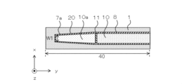
実施の形態1について図面を用いて以下に説明する。図1は、実施の形態1に係る半導体装置100全体の上面構成を模式的に示す平面図である。図1に示すように、半導体装置100には、半導体スイッチング素子が構成される活性領域30と、活性領域30の周囲に外周領域40が存在している。さらに、トレンチ7が活性領域30から外周領域40に向かって、Y方向に延伸するように設けられている。Y方向をトレンチ7の延伸方向とする。また、複数のトレンチ7が、トレンチ7の延伸方向と直行する方向であるX方向において隣り合うように設けられている。図1では、トレンチ7の数を5個で示しているが、トレンチ7の数は、これに限るものではない。また、本実施形態では、スプリットゲートのトレンチ構造を有し、半導体スイッチング素子として、絶縁ゲート型バイポーラトランジスタ(Insulated Gate Bipolar Transistor:以下、IGBTと略する)を用いる半導体装置を例に挙げて説明する。以下、図2~図5に基づいて本実施形態の半導体装置100の詳細な構造について説明する。
The first embodiment will be described below with reference to the drawings. FIG. 1 is a plan view showing a schematic top surface configuration of a
図2は、実施の形態1に係る半導体装置100の活性領域30におけるトレンチ7延伸方向と直行する方向の断面図である。なお、図2は、図1に示された一点鎖線A―Aにおける断面を示している。図3は、実施の形態1に係るトレンチ7延伸方向と平行な方向の断面図である。なお、図3は、図1に示された一点鎖線B-Bにおける断面を示している。図4は、実施の形態1に係る半導体装置100のトレンチ7の外周部における平面図である。なお、図4は、図1に示された領域Cにおける拡大図および、図2に示された点線Cにおける平面図を示している。図5は、図4で示されたトレンチ7の変形例を示す平面図である。
Figure 2 is a cross-sectional view in a direction perpendicular to the extension direction of the
まず、図2、図3を用いて、半導体装置100の断面構成を説明する。図2に示すように、半導体装置100は、活性領域30において半導体スイッチング素子が構成されている。半導体スイッチング素子は、n-型ドリフト層1、n型キャリア蓄積層2、p型ベース層3、n+型ソース層4、n型バッファ層5、p型コレクタ層6、トレンチ7、上部絶縁膜8a、下部絶縁膜8b、上部電極9、下部電極10、境界絶縁膜11、層間絶縁膜12、エミッタ電極13およびコレクタ電極14を含む。また、図3に示すように、外周領域40において、ゲート電極15が設けられている。
First, a cross-sectional configuration of the
活性領域30における半導体基板の第1主面は、n+型ソース層4および図示しないp+型コンタクト層の表面(上面)に対応する。第1主面は、半導体基板の上面である。半導体基板の第2主面は、p型コレクタ層6の表面(下面)に対応する。第2主面は、第1主面とは反対側の面であって半導体基板の下面である。図2において、半導体基板はn+型ソース層4およびp+型コンタクト層の上面からp型コレクタ層6の下面までの範囲に対応する。
The first main surface of the semiconductor substrate in the
n-型ドリフト層1は、半導体基板からなる。n-型ドリフト層1は、半導体基板の第1主面と第2主面との間に設けられている。n-型ドリフト層1は、n型不純物として例えばヒ素またはリン等を含む半導体層であり、n型不純物の濃度は、好ましくは、1.0E+12/cm3以上1.0E+15/cm3以下である。
The n -type drift layer 1 is made of a semiconductor substrate. The n -
n型キャリア蓄積層2は、n-型ドリフト層1に対して半導体基板の第1主面側に設けられている。n型キャリア蓄積層2は、n型不純物として例えばヒ素またはリン等を有する半導体層であり、n型不純物の濃度は、好ましくは、1.0E+13/cm3以上1.0E+17/cm3以下である。n型キャリア蓄積層2を設けることによって、電流が流れた際の通電損失を低減できる。なお、半導体装置100は、n型キャリア蓄積層2が設けられずに、n型キャリア蓄積層2の領域にもn-型ドリフト層1が設けられた構成であってもよく、n型キャリア蓄積層2とn-型ドリフト層1とを合わせてドリフト層と定められていてもよい。
The n-type
p型ベース層3は、n型キャリア蓄積層2に対して半導体基板の第1主面側に設けられている。p型ベース層3は、p型不純物として、例えばボロンまたはアルミニウム等を含む半導体層であり、p型不純物の濃度は、好ましくは、1.0E+12/cm3以上1.0E+19/cm3以下である。p型ベース層3は、トレンチ7の上部絶縁膜8aに接している。上部電極9にゲート駆動電圧が印加された場合、p型ベース層3にチャネルが形成される。
The p-type base layer 3 is provided on the first main surface side of the semiconductor substrate with respect to the n-type
n+型ソース層4は、p型ベース層3に対して半導体基板の第1主面側に設けられている。そのn+型ソース層4は、半導体基板の表層として、p型ベース層3の上方に選択的に設けられている。n+型ソース層4は、n型不純物として、例えばヒ素またはリン等を含む半導体層であり、n型不純物の濃度は、好ましくは、1.0E+17/cm3以上1.0E+20/cm3以下である。n+型ソース層4は、トレンチ7の上部絶縁膜8aに接している。また、n+型ソース層4は、n+型エミッタ層と言われる場合がある。
The n +
p+型コンタクト層は、図示はしないが、p型ベース層3に対して半導体基板の第1主面側に設けられている。そのp+型コンタクト層は、半導体基板の表層として、p型ベース層3の上方に選択的に設けられている。p+型コンタクト層は、p型ベース層3の上方において、トレンチ7の延伸方向に沿って、n+型ソース層4が設けられていない領域に設けられている。p+型コンタクト層は、p型不純物として、例えばボロンまたはアルミニウム等を含む半導体層であり、p型不純物の濃度は、好ましくは、1.0E+15/cm3以上1.0E+20/cm3以下である。なお、p+型コンタクト層は、p型ベース層3よりもp型不純物の濃度が高い領域であり、p+型コンタクト層とp型ベース層3とを区別する必要がある場合にはそれぞれを個別に呼称してよく、p+型コンタクト層とp型ベース層3とを合わせて1つのp型ベース層3と定められていてもよい。
Although not shown, the p + type contact layer is provided on the first main surface side of the semiconductor substrate with respect to the p type base layer 3. The p + type contact layer is selectively provided above the p type base layer 3 as a surface layer of the semiconductor substrate. The p + type contact layer is provided above the p type base layer 3 along the extension direction of the
n型バッファ層5は、n-型ドリフト層1に対して半導体基板の第2主面側に設けられている。n型バッファ層5は、n型不純物として、例えばリンおよびプロトンのうち少なくとも一方を含む半導体層であり、n型不純物の濃度は、好ましくは、1.0E+12/cm3以上1.0E+18/cm3以下である。n型バッファ層5は、n-型ドリフト層1よりもn型不純物の濃度が高い。n型バッファ層5は、半導体装置100がオフ状態の場合に、空乏層がp型ベース層3から第2主面側に伸びパンチスルーが発生することを低減する。n型バッファ層5とn-型ドリフト層1とは、合わせて1つのn-型ドリフト層1と定められていてもよい。さらには、n型キャリア蓄積層2とn型バッファ層5とn-型ドリフト層1とが、合わせて1つのn-型ドリフト層1と定められていてもよい。また、n型バッファ層5は、必ずしも必要ではなく、n型バッファ層5の領域にn-型ドリフト層1が設けられていてもよい。
The n-type buffer layer 5 is provided on the second main surface side of the semiconductor substrate with respect to the n -
p型コレクタ層6は、n型バッファ層5に対して半導体基板の第2主面側に設けられている。p型コレクタ層6は、p型不純物として、例えばボロンまたはアルミニウム等を含む半導体層であり、p型不純物の濃度は、好ましくは、1.0E+16/cm3以上1.0E+20/cm3以下である。
The p-
トレンチ7は、半導体基板の第1主面、つまり半導体基板の上面に設けられている。トレンチ7は、半導体基板の第1主面からn+型ソース層4と、p型ベース層3を厚み方向に貫通し、n-型ドリフト層1に達している。
The
また、トレンチ7の内壁面は、絶縁膜8によって覆われている。絶縁膜8については、単独の膜で構成されていても良いが、本実施形態の場合は、トレンチ7のうちの上方部分を覆っている上部絶縁膜8aと下方部分を覆っている下部絶縁膜8bとによって構成されている。上部絶縁膜8aは、トレンチ7の上方部分の側面を覆い、下部絶縁膜8bは、トレンチ7の底部から下方部分の側面を覆っている。上部絶縁膜8a、下部絶縁膜8bは、例えば、酸化膜である。なお、下部絶縁膜8bの厚みを上部絶縁膜8aの厚みよりも厚くしてもよい。このような構成にすることで、後述するトレンチ端部7aにおいて、電界集中による絶縁膜破壊を抑制できる。
The inner wall surface of the
さらに、トレンチ7は、内部に上部電極9と下部電極10の2つの電極を有する2段構造、すなわちスプリットゲート構造を有している。トレンチ7内には、上部絶縁膜8aを介して上部電極9が設けられ、上部電極9の第2主面側には下部絶縁膜8bを介して下部電極10が設けられている。また、境界絶縁膜11によって上部電極9と下部電極10とが絶縁されている。つまり、トレンチ7の内部において、絶縁膜を介して、下部電極、境界絶縁膜、および上部電極が順に積層されて2段構造をなしている。ここで、下部電極10は、下部絶縁膜8bを介してn-型ドリフト層1に対向している。なお、上部電極9の底部はp型ベース層3よりも第2主面側に位置している。
Furthermore, the
上部電極9、下部電極10は、n型またはp型の不純物をドープしたポリシリコンを堆積させて形成されており、ポリシリコンの不純物の濃度は1.0E+17/cm3~1.0E+22/cm3であり、下部電極10の不純物濃度は上部電極9よりも高濃度であり、例えば1.0E+19/cm3~1.0E+22/cm3である。好ましくは、1.0E+20/cm3~1.0E+22/cm3である。
The
また、図3に示すように、上部電極9は外周領域40においてゲート電極15と電気的に接続され、下部電極10は活性領域30においてエミッタ電極13と電気的に接続されている。さらに、外周領域40に位置するトレンチ7の延伸方向の外周部において、下部電極10は、上部電極9よりも外側まで延設されている。下部電極10のうち、上部電極9よりも外側まで延設されている部分を下部電極10の延設部10aとする。そして、延設部10aが、半導体基板の第1主面まで、上部電極9の端部を覆うようにさらに延設されている。なお、延設部10aと上部電極9との間も境界絶縁膜11によって絶縁されている。また、下部電極10のうち、下部電極10をエミッタ電極13に電気的に接続するための部分を引上げ領域部10bとする。引き上げ領域部10bは、半導体基板の第1主面まで、上部電極9を貫通するようにさらに延設されている。なお、引き上げ領域部10bと上部電極9との間も境界絶縁膜11によって絶縁されている。
3, the
また、図3に示すように、層間絶縁膜12は、トレンチ7の上部電極9、下部電極10上に設けられている。
Also, as shown in FIG. 3, the
図示はしないがバリアメタルは、半導体基板の第1主面のうち、層間絶縁膜12が設けられていない領域上および層間絶縁膜12上に形成されている。バリアメタルは、例えばチタンを含む導電体で形成されている。チタンを含む導電体とは、例えば、窒化チタン、TiSiである。TiSiは、チタンとシリコン(Si)との合金である。バリアメタルは、n+型ソース層4、p+型コンタクト層および下部電極10にオーミック接触している。バリアメタルは、n+型ソース層4、p+型コンタクト層および下部電極10に電気的に接続されている。
Although not shown, the barrier metal is formed on the region of the first main surface of the semiconductor substrate where the
エミッタ電極13は、活性領域30に設けられたバリアメタル上に設けられる。エミッタ電極13は、例えば、アルミシリコン合金(Al―Si系合金)で形成される。エミッタ電極13は、バリアメタルを介して、n+型ソース層4、p+型コンタクト層および下部電極10に電気的に接続されている。エミッタ電極13は、アルミニウム合金膜およびその他の金属膜からなる複数の金属膜で構成されていてもよい。例えば、エミッタ電極13は、アルミニウム合金膜とめっき膜とで構成されていてもよい。めっき膜は、例えば、無電解めっきあるいは電解めっきで形成される。めっき膜は、例えば、ニッケル(Ni)膜である。互いに隣接する層間絶縁膜12の間の微細領域には、タングステン膜が形成されていてもよい。エミッタ電極13は、そのタングステン膜上に形成される。タングステン膜は、めっき膜よりも埋込性が良好であるため、良好なエミッタ電極13が形成される。
The
なお、バリアメタルとエミッタ電極13とが、合わせて1つのエミッタ電極13と定められていてもよい。また、バリアメタルは必ずしも設ける必要はない。バリアメタルが設けられない場合、エミッタ電極13は、n+型ソース層4上、p+型コンタクト層上および下部電極10上に設けられ、それらとオーミック接触する。または、バリアメタルは、n+型ソース層4などのn型半導体層上のみに設けてられてもよい。下部電極10上の一部には、層間絶縁膜12が設けられていてもよい。その場合、エミッタ電極13は、下部電極10上のいずれかの領域において、その下部電極10と電気的に接続される。
The barrier metal and the
また、図3に示すように、ゲート電極15は、外周領域40においてn-型ドリフト層1上および上部電極9上に設けられ、それらとオーミック接触する。また、上部電極9上の一部には、層間絶縁膜12が設けられていてもよい。その場合、ゲート電極15は、上部電極9上のいずれかの領域において、その上部電極9と電気的に接続される。
3, the
コレクタ電極14は、p型コレクタ層6に対して半導体基板の第2主面側に設けられている。コレクタ電極14は、例えば、エミッタ電極13と同様に、アルミニウム合金で形成される。コレクタ電極14は、p型コレクタ層6にオーミック接触し、そのp型コレクタ層6に電気的に接続されている。コレクタ電極14は、アルミニウム合金とめっき膜とで構成されていてもよい。また、コレクタ電極14は、エミッタ電極13とは異なる構成であってもよい。
The
以上のようにして、IGBTを有する半導体装置100が構成されている。続いて、上述したトレンチ7の構造のうちのトレンチ7の延伸方向の外周部の構造の詳細について、図4を参照して説明する。
In this manner, the
図4に示すように、トレンチ7のうち下部電極10の延設部10aに対応する領域をトレンチ端部7aとする。トレンチ端部7aにおいて、トレンチ幅が最も狭くなるようにされている。ここで、トレンチ端部7aの幅を第1幅W1とし、トレンチ幅はトレンチ端部7aにおいて最小のW1となる。
As shown in FIG. 4, the region of the
上述した構成とすることで、半導体装置100のアバランシェ耐圧の向上を可能にしている。この理由について、以下に説明する。
The above-mentioned configuration makes it possible to improve the avalanche breakdown voltage of the
まず、IGBTにおけるオン状態では、n-型ドリフト層1に向かって大量の電子とホールが流入する。次にターンオフスイッチング時において、n-型ドリフト層1への電子とホールの流入は停止する。ここで、n-型ドリフト層1に流入したホールは、排出経路が存在しない外周領域40から、ホールが排出されるエミッタ電極13に向けて流れ込む。つまり、トレンチ端部7aにも高密度でホールが流れ込み、トレンチ端部7aのホール密度が増加する。電子の流入は停止しているため、トレンチ端部7aでの空間電荷密度が増加し、電界強度が増加することでアバランシェが発生する。
First, in the on state of the IGBT, a large amount of electrons and holes flow toward the n -
上述したように、トレンチ端部7aにおいてトレンチ幅を最も狭いW1とする構成にすることで、トレンチ端部7aにおいて、トレンチとトレンチの間の領域であるメサ幅WMを広くできるため、ホールの排出経路を拡大できホール密度を低減できる。これにより空間電荷密度を低減でき、電界強度の増加を抑制しアバランシェ耐圧を向上できる。
As described above, by configuring the trench width W1 to be the narrowest at the
また、下部電極10はエミッタ電極13に電気的に接続されているため、上部電極9に比べて電位が低い。そのため、ターンオフスイッチング時において、トレンチ7のうち上部電極9に対応する領域の側壁だけではなく、下部電極10に対応する領域の側壁にもホールが引き寄せられる。上述したように、下部電極10の延設部10aをトレンチ7内の先端部に配置する構成とすることで、トレンチ端部7aの側壁にもホールを引き寄せ、n-型ドリフト層1内に低抵抗なp型反転層を形成できる。つまり、トレンチ端部7aにおいて、ホールは低抵抗なp型反転層を通過できるためホールの排出が促進される。
In addition, since the
次に実施の形態1の変形例について、図5を用いて説明する。図5に示すように、トレンチ幅が最も狭くなる領域を、トレンチ7のうち、延設部10aに対応する領域に加えて上部電極9の一部に対応する領域までとしてもよい。ここで、上部電極9の一部に対応する領域は、外周領域40内に存在する上部電極9に対応する領域とする。このような構成とすることで、トレンチ7においてトレンチ幅を最も狭いW1とする領域が拡大する。したがって、メサ幅WMが広い領域が拡大するため、さらにホール密度を低減でき、アバランシェ耐圧を向上できる。
Next, a modification of the first embodiment will be described with reference to Fig. 5. As shown in Fig. 5, the region where the trench width is narrowest may be the region of the
以上説明したように、本実施形態の半導体装置100では、トレンチ幅を変化させることでメサ幅を変化させ、トレンチ端部7aのメサ幅が最も大きくなるようにしている。これにより、トレンチ端部7aでのホール密度を低減でき、スプリットゲート構造のIGBTを有する半導体装置100において、アバランシェ耐圧の向上を実現できる。
As described above, in the
さらに、本実施形態の半導体装置100では、ホールの排出経路を拡大できるため、ホールが排出されやすくなり、ターンオフ損失を低減できる。したがって、ターンオフ損失を低減することで、スプリットゲート構造のIGBTを有する半導体装置100において、スイッチング損失を低減できる。
Furthermore, in the
なお、本実施形態の半導体装置100の製造方法については、基本的には従来からのスプリットゲート型トレンチ構造を有するIGBTが備えられた半導体装置100の製造方法と同様である。ただし、トレンチ7を形成する際のエッチング工程の際に、トレンチ7のうち、少なくともトレンチ端部7aにおけるトレンチ幅を最も狭いW1とするエッチングマスクを用いるようにする。
The manufacturing method of the
半導体装置100の製造方法について詳細な説明をする。半導体装置100の製造方法は、半導体基板を準備する工程、半導体基板の第1主面側を形成する工程、半導体基板の第2主面側を形成する工程を備える。
A detailed description will now be given of the method for manufacturing the
まず、半導体基板を準備する工程を説明する。本実施形態では、半導体基板として、n型不純物を含むn型ウエハが準備される。半導体基板は、FZ(Floating Zone)法で作製された、いわゆるFZウエハであってもよいし、MCZ(Magnetic field applied CZochralki)法で作製された、いわゆるMCZウエハであってもよい。または、半導体基板は、昇華法あるいはCVD(chemical vapor deposition)によって作製されたウエハであってもよい。この工程においては、その半導体基板全体がn-型ドリフト層1に対応する。n型不純物の濃度は、半導体装置100の耐圧仕様によって適宜選択される。例えば、半導体装置100の耐圧仕様が1200Vである場合、n型不純物の濃度はn-型ドリフト層1の比抵抗が40~120Ω・cm程度となるように調整される。本実施形態では、半導体基板全体がn-型ドリフト層1であるn型ウエハを準備する工程を示すが、半導体基板を準備する工程はそれに限定されるものではない。例えば、半導体基板の第1主面または第2主面からn型不純物をイオン注入する工程と、熱処理によってそのn型不純物を拡散させる工程とによって、n-型ドリフト層1を含む半導体基板が準備されてもよい。
First, the process of preparing a semiconductor substrate will be described. In this embodiment, an n-type wafer containing n-type impurities is prepared as the semiconductor substrate. The semiconductor substrate may be a so-called FZ wafer produced by the FZ (Floating Zone) method, or a so-called MCZ wafer produced by the MCZ (Magnetic field applied CZochralki) method. Alternatively, the semiconductor substrate may be a wafer produced by sublimation or chemical vapor deposition (CVD). In this process, the entire semiconductor substrate corresponds to the n -
次に、半導体基板の第1主面側を形成する工程を説明する。まず、n型キャリア蓄積層2を形成するためのn型不純物が半導体基板の第1主面側からn-型ドリフト層1の表層にイオン注入される。そのn型不純物は、例えばリンである。次に、p型ベース層3を形成するためのp型不純物が半導体基板の第1主面側からイオン注入される。そのp型不純物は、例えばボロンである。イオン注入後に熱処理が施され、n型不純物およびp型不純物は拡散し、n型キャリア蓄積層2、p型ベース層3が形成される。
Next, a process for forming the first main surface side of the semiconductor substrate will be described. First, n-type impurities for forming the n-type
上記のイオン注入の際、半導体基板の第1主面上には、所定の領域に開口を有するマスクが形成される。n型不純物およびp型不純物は、マスクの開口に対応した領域に注入される。そのマスクは、半導体基板の第1主面上にレジストを塗布する工程、および、フォトリソグラフィー(写真製版)技術によってレジストの所定の領域に開口を形成する工程によって形成される。以下、このような所定の領域に開口を有するマスクを形成する処理を、マスク処理と言う。n型不純物およびp型不純物は、マスク処理によって所定の領域に注入される。その結果、n型キャリア蓄積層2、p型ベース層3は、半導体基板の第1主面の面内に選択的に形成される。
During the above ion implantation, a mask having openings in predetermined regions is formed on the first main surface of the semiconductor substrate. N-type impurities and p-type impurities are implanted into regions corresponding to the openings in the mask. The mask is formed by a process of applying resist to the first main surface of the semiconductor substrate and a process of forming openings in predetermined regions of the resist by photolithography (photoengraving) technology. Hereinafter, the process of forming a mask having openings in such predetermined regions is referred to as mask processing. N-type impurities and p-type impurities are implanted into the predetermined regions by the mask processing. As a result, the n-type
次に、n+型ソース層4を形成されるためのn型不純物が半導体基板の第1主面側からp型ベース層3の表層にイオン注入される。この際、n型不純物はマスク処理によって注入され、n+型ソース層4がp型ベース層3の表層に選択的に形成される。n型不純物は、例えば、砒素またはリンである。
Next, an n-type impurity for forming an n +
次に、p+型コンタクト層を形成されるためのp型不純物が、半導体基板の第1主面側からp型ベース層3の表層にイオン注入される。この際、p型不純物はマスク処理によって注入され、p+型コンタクト層がp型ベース層3の表層にそれぞれ選択的に形成される。p型不純物は、例えば、ボロンまたはアルミニウムである。 Next, p-type impurities for forming a p + -type contact layer are ion-implanted from the first main surface side of the semiconductor substrate into the surface layer of the p-type base layer 3. At this time, the p-type impurities are implanted using a mask process, and the p + -type contact layer is selectively formed on the surface layer of the p-type base layer 3. The p-type impurities are, for example, boron or aluminum.
次に、半導体基板の第1主面からn+型ソース層4およびp型ベース層3を貫通し、n-型ドリフト層1に達するトレンチ7を形成する。活性領域30において、n+型ソース層4を貫通するトレンチ7は、側壁がn+型ソース層4の一部を構成する。
Next,
トレンチ7を形成するために、まず、半導体基板の第1主面に酸化膜を堆積させる。酸化膜は例えばSiO2などの薄膜である。次に、トレンチ7を形成する部分の酸化膜に開口を形成し、開口を有するマスクを形成する。なお、マスク形成の際は、トレンチ7のうち、トレンチ端部7aにおけるトレンチ幅が最も狭い幅W1になるような開口を有したマスクを形成する。最後に、マスクを介して半導体基板をエッチングすることでトレンチ7が形成される。
To form the
次に、酸素を含む雰囲気中で半導体基板を加熱し、トレンチ7の内壁および半導体基板の第1主面に下部絶縁膜8bを形成する。なお、半導体基板の第1主面に形成された下部絶縁膜8bは後の工程で除去される。
Next, the semiconductor substrate is heated in an atmosphere containing oxygen to form a lower insulating
次に、内壁に下部絶縁膜8bを形成したトレンチ7内部に、下部電極10を形成する。n型またはp型の不純物がドープされたポリシリコンが、CVD(chemical vapor deposition)などによってトレンチ7の内部に堆積させて下部電極10を形成する。その結果、下部電極10が、下部絶縁膜8bを介してトレンチ7の内部に形成される。
Next, a
次に、マスク処理によって上部電極9を充填させるトレンチ7を開口したマスクを形成し、トレンチ7内の下部電極10をエッチングする。その後、トレンチ7内の下部絶縁膜8bのうち上部絶縁膜8aが形成される部分を除去する。
Next, a mask is formed by mask processing to open the
次に、酸素を含む雰囲気中で半導体基板を加熱し、トレンチ7の内壁および半導体基板の第1主面に上部絶縁膜8aを形成する。また、下部電極10の第1主面に境界絶縁膜11を形成する。なお、半導体基板の第1主面に形成された上部絶縁膜8aは後の工程で除去される。
Next, the semiconductor substrate is heated in an atmosphere containing oxygen to form an upper insulating film 8a on the inner wall of the
次に、内壁に上部絶縁膜8aを形成したトレンチ7内部に、上部電極9を形成する。n型またはp型の不純物がドープされたポリシリコンが、CVD(chemical vapor deposition)などによってトレンチ7の内部に堆積させて上部電極9を形成する。その結果、上部電極9が、上部絶縁膜8aを介してトレンチ7の内部に形成される。
Next, an
次に、層間絶縁膜12をトレンチ7上に形成する。層間絶縁膜12は、マスク処理により堆積され、半導体基板の第1主面に形成された酸化膜は除去される。層間絶縁膜12は、例えば、酸化膜としてSiO2を含む。
Next, the
そして、コンタクトホールを層間絶縁膜12に形成する。コンタクトホールは、n+型ソース層4上、p+型コンタクト層上に形成される。
Then, contact holes are formed in the
次に、バリアメタルを、半導体基板の第1主面および層間絶縁膜12上に形成する。バリアメタルは、PVD(physical vapor deposition)またはCVDによって製膜される。
Next, a barrier metal is formed on the first main surface of the semiconductor substrate and the
次に、エミッタ電極13を、バリアメタル上に形成する。エミッタ電極13は、スパッタリング、蒸着等のPVD法によって形成される。エミッタ電極13は、例えば、アルミシリコン合金(Al-Si系合金)を含む。さらに、第2のエミッタ電極13をエミッタ電極13の上に無電解めっき法あるいは電解めっき法によって形成してもよい。第2のエミッタ電極13は、例えば、ニッケルまたはニッケル合金を含む。第2のエミッタ電極13は、例えば、2種類以上の金属層を含む積層構造を有していてもよい。その積層構造は、例えば、Ni膜、Pd膜およびAu膜で構成され、めっき法で形成される。
Next, the
めっき法は、厚い金属膜を容易に形成することを可能にする。厚膜のエミッタ電極13においては、熱容量が増加するため、エミッタ電極13の耐熱性が向上する。なお、アルミシリコン合金上に、めっき処理でニッケル合金をさらに形成する場合、そのめっき処理は半導体基板の第2主面側の加工が行われた後に実施してもよい。
Plating makes it possible to easily form a thick metal film. In a
次に、半導体基板の第2主面側を形成する工程を説明する。まず、半導体基板を薄板化する工程を説明する。半導体基板の第2主面を研削し、半導体装置100の設計に応じた所定の厚さに薄板化する。研削後の半導体基板の厚さは、例えば、80μm以上200μm以下である。
Next, the process of forming the second main surface side of the semiconductor substrate will be described. First, the process of thinning the semiconductor substrate will be described. The second main surface of the semiconductor substrate is ground to thin it to a predetermined thickness according to the design of the
次に、n型バッファ層5およびp型コレクタ層6を形成する工程を説明する。まず、n型バッファ層5を形成するためのn型不純物が、薄板化された半導体基板の第2主面側からn-型ドリフト層1の表層にイオン注入される。n型不純物として、例えば、リンが注入されてもよいし、プロトンが注入されてもよい。または例えば、リンおよびプロトンの両方が注入されてもよい。
Next, a process for forming the n-type buffer layer 5 and the p-
プロトンは、比較的低い加速エネルギーで半導体基板の第2主面から深い位置にまで注入される。プロトンの注入深さは、加速エネルギーの変更によって比較的容易に制御される。このため、加速エネルギーを変更しながら、プロトンが複数回イオン注入された場合、リンを含むn型バッファ層5よりも、半導体基板の厚さ方向に幅が広いn型バッファ層5が形成される。 Protons are implanted deep into the second main surface of the semiconductor substrate with a relatively low acceleration energy. The depth of proton implantation can be controlled relatively easily by changing the acceleration energy. Therefore, when protons are ion-implanted multiple times while changing the acceleration energy, an n-type buffer layer 5 is formed that is wider in the thickness direction of the semiconductor substrate than an n-type buffer layer 5 containing phosphorus.
また、リンは、プロトンと比較して、n型不純物としての活性化率が高い。薄板化した半導体基板であっても、リンを含むn型バッファ層5は、より確実に空乏層の拡大によるパンチスルーの発生を低減させる。半導体基板をより一層薄板化するためには、プロトンおよびリンの両方を含むn型バッファ層5が形成されることが好ましい。その場合、プロトンはリンよりも半導体基板の第2主面から深い位置に注入される。 In addition, phosphorus has a higher activation rate as an n-type impurity compared to protons. Even in a thin semiconductor substrate, an n-type buffer layer 5 containing phosphorus more reliably reduces the occurrence of punch-through due to the expansion of the depletion layer. In order to further thin the semiconductor substrate, it is preferable to form an n-type buffer layer 5 containing both protons and phosphorus. In that case, protons are implanted deeper from the second main surface of the semiconductor substrate than phosphorus.
次に、p型コレクタ層6を形成するためのp型不純物が、半導体基板の第2主面側からイオン注入される。p型不純物として、例えば、ボロンが注入される。イオン注入後、半導体基板の第2主面にレーザーが照射される。そのレーザーアニールによって、注入されたボロンが活性化し、p型コレクタ層6が形成される。
Next, p-type impurities for forming the p-
このレーザーアニールの際、半導体基板の第2主面から比較的浅い位置に注入されたn型不純物のリンも同時に活性化される。一方プロトンは、350℃~500℃程度の比較的低いアニール温度で活性化される。そのため、プロトンが注入された後、そのプロトンの活性化の工程以外で、半導体基板が350℃~500℃よりも高い温度に加熱されないことが好ましい。レーザーアニールは、半導体基板の第2主面近傍のみを高温に加熱する。そのため、レーザーアニールは、プロトンの注入後におけるn型不純物またはp型不純物の活性化に有効である。 During this laser annealing, the n-type impurity phosphorus implanted at a relatively shallow position from the second main surface of the semiconductor substrate is also activated at the same time. On the other hand, protons are activated at a relatively low annealing temperature of about 350°C to 500°C. Therefore, after the protons are injected, it is preferable that the semiconductor substrate is not heated to a temperature higher than 350°C to 500°C except during the proton activation process. Laser annealing heats only the vicinity of the second main surface of the semiconductor substrate to a high temperature. Therefore, laser annealing is effective in activating n-type or p-type impurities after proton injection.
次に、コレクタ電極14を形成する工程を説明する。コレクタ電極14は、半導体基板の第2主面に形成される。コレクタ電極14は、半導体基板の第2主面の全面に亘って形成されてもよい。コレクタ電極14は、アルミシリコン合金、チタン等を含む。コレクタ電極14は、スパッタリング、蒸着等のPVDによって形成される。コレクタ電極14は、各々がアルミシリコン合金、チタン、ニッケルあるいは金などを含む複数の金属層で形成されていてもよい。または、コレクタ電極14は、PVDによって形成された金属膜上に、無電解めっきあるいは電解めっきによって別の金属膜が形成された構造を有していてもよい。
Next, the process of forming the
上記した工程により、半導体装置100は作製される。半導体装置100は、1枚のn型ウエハにマトリクス状に複数作製されるので、レーザーダイシングまたはブレードダイシングにより個々の半導体装置100に切り分けることで半導体装置100は完成する。
The
実施の形態2.
実施の形態2における半導体装置について図6、7を用いて説明する。図6、7は、図4、5と同様に、トレンチ7の外周部における平面図を示している。ここで、図6に示すように、トレンチ7のうち、トレンチ端部7aの幅を第1幅W1とする。また、トレンチ7のうち、トレンチ幅が最も広くなる領域のトレンチ幅を第2幅W2とする。実施の形態2の半導体装置は、実施の形態1と同様にトレンチ7が、トレンチ端部7aにおいてトレンチ幅が最も狭くなるように形成される。さらに、トレンチ端部7aのトレンチ幅は、トレンチ7のうちトレンチ幅が最も広くなる領域の幅よりも狭いことを特徴としている。つまり、トレンチ7はトレンチ幅がW1<W2となるように形成され、さらにトレンチ幅がW2からW1となるようにトレンチ端部7aの先端に向かうにつれて、トレンチ幅が徐々に狭くなっている。実施の形態2では、トレンチ幅が最も広くなる領域は、トレンチ7のうち、外周領域における上部電極9の一部に対応する領域とする。
A semiconductor device in the second embodiment will be described with reference to FIGS. 6 and 7. FIGS. 6 and 7 show plan views of the outer periphery of the
上述した構成とすることで、トレンチ幅が狭くなる領域においてメサ幅が拡大するため、ホールの排出経路を拡大できる。したがって、ホール排出が促進されるため、ホールが排出しづらいトレンチ幅が最も広くなる領域でのホール密度の増加を抑制し、アバランシェ耐圧を向上できる。 The above-mentioned configuration expands the mesa width in the region where the trench width is narrow, allowing the hole discharge path to be expanded. This promotes hole discharge, suppressing the increase in hole density in the region where the trench width is at its widest, where holes are difficult to discharge, and improving the avalanche breakdown voltage.
また、図7に示すように、トレンチ幅が最も広くなる領域が、上部電極9をゲート電極15に電気的に接続する引上げ領域50に存在し、トレンチ7のうち、活性領域30内に存在する上部電極9に対応するトレンチ幅よりも引き上げ領域50におけるトレンチ幅が広くなる場合が考えられる。なぜならば、上部電極9をゲート電極15に電気的に接続するためのコンタクトホールを配置する面積分だけ引上げ領域50のトレンチ幅は広くなるからである。したがって、引き上げ領域50でのメサ幅が狭くなるため、ホール密度が増加し、アバランシェ耐圧が低下しやすい。
Also, as shown in FIG. 7, the area where the trench width is the widest may exist in the pull-up
この場合において、図7に示すように、トレンチ幅が最も広くなる領域である引上げ領域50のトレンチ幅をW2、トレンチ幅が最も狭くなる領域であるトレンチ端部7aのトレンチ幅をW1とし、W1<W2となるようにする。さらにW2からW1となるようにトレンチ端部7aに向かって、トレンチ幅を徐々に狭くする。
In this case, as shown in FIG. 7, the trench width of the pulled-up
上述した構成とすることで、引上げ領域50を除く領域において、メサ幅が拡大するためホールの排出経路を拡大できる。したがって、ホール排出が促進されるため、ホールが排出しづらい引上げ領域50でのホール密度の増加を抑制し、アバランシェ耐圧を向上できる。
The above-mentioned configuration expands the mesa width in the region other than the pulling
上述したように、実施の形態2に係る半導体装置では、実施の形態1と同様な効果に加えて、ホールが排出しづらいトレンチ幅が最も広くなる領域が存在する場合でも、ホール密度の増加を抑制し、アバランシェ耐圧を向上できる。 As described above, in the semiconductor device according to the second embodiment, in addition to the same effects as those of the first embodiment, even when there is a region where the trench width is the widest and where holes are difficult to discharge, the increase in hole density can be suppressed and the avalanche breakdown voltage can be improved.
実施の形態3.
実施の形態3における半導体装置について図8から図10を用いて説明する。図8から図10は、図4、5と同様に、トレンチ7の外周部における平面図を示している。ここで、実施の形態3の半導体装置は、実施の形態1と同様にトレンチ端部7aの幅を第1幅W1とし、トレンチ端部7aにおけるトレンチ幅が最小のW1となるように形成される。さらに、トレンチ端部7aにおいて、トレンチ端部7aの先端に向かうにつれて、トレンチ幅が徐々に狭くなることを特徴としている。
Embodiment 3.
A semiconductor device according to the third embodiment will be described with reference to Figures 8 to 10. Figures 8 to 10 show plan views of the outer periphery of
図8に示すように、実施の形態3の半導体装置は、トレンチ幅は2回以上の段差によって狭くなり、トレンチ端部7aにおいて最小のW1となる。段階的に狭くすることで、トレンチ7におけるホール密度の偏りを小さくでき、電界集中を緩和できるため、さらに、アバランシェ耐圧を向上できる。
As shown in FIG. 8, in the semiconductor device of the third embodiment, the trench width is narrowed by two or more steps, and is at a minimum W1 at the
また、図9に示すように、トレンチ端部7aにテーパー20を設けてもよい。テーパー20を付けることで、トレンチ7の幅をトレンチ7の先端に向かうにつれて徐々に狭くできる。つまり、トレンチ端部7aにおいて、トレンチ7の幅を最小のW1とすることができる。上述した構成により、トレンチ7におけるホール密度の偏りを小さくでき、電界集中を緩和できるため、さらにアバランシェ耐圧を向上できる。また、図9では、トレンチ端部7aのみにテーパーが付けられているが、トレンチ7のうち上部電極9に対応する領域にもテーパーが付けられていてもよい。
As shown in FIG. 9, a
また、図10に示すように、トレンチ端部7aの先端は丸く形成された構成としてもよい。トレンチ端部7aの先端が角形状の場合、トレンチ端部7aに電界が集中しやすい。トレンチ端部7aの角を無くし、丸く形成されることで、トレンチ7の幅をトレンチ7の先端に向かうにつれて徐々に狭くできる。つまり、トレンチ端部7aにおいて、トレンチ7の幅を最小のW1とすることができる。上述した構成により、トレンチ7におけるホール密度の偏りを小さくでき、電界集中を緩和できるため、さらにアバランシェ耐圧を向上できる。
Also, as shown in FIG. 10, the tip of the
上述したように、実施の形態3に係る半導体装置では、実施の形態1と同様な効果に加えて、ホール密度の偏りを抑制し、電界集中を緩和できるため、さらにアバランシェ耐圧を向上できる。 As described above, in the semiconductor device according to the third embodiment, in addition to the same effects as those of the first embodiment, the bias in hole density can be suppressed and the electric field concentration can be alleviated, thereby further improving the avalanche breakdown voltage.
実施の形態4.
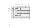
実施の形態4における半導体装置について図11を用いて説明する。図11は、図4、5と同様に、トレンチ7の外周部における平面図を示している。実施の形態4の半導体装置は、実施の形態1と同様にトレンチ端部7aの幅を第1幅W1とし、トレンチ端部7aにおけるトレンチ幅が最小のW1となるように形成される。さらに、延設部10aのそれぞれが、トレンチ7の延伸方向と交差する方向であるX方向に延伸する交差トレンチ21によって接合され、隣り合う下部電極10同士が繋がることを特徴とする。
A semiconductor device according to the fourth embodiment will be described with reference to Fig. 11. Fig. 11 shows a plan view of the outer periphery of the
交差トレンチ21の内壁面は、絶縁膜によって覆われている。絶縁膜については、上部絶縁膜8aと下部絶縁膜8bと同様の単独の膜で構成されていても良いが、実施の形態4では、交差絶縁膜22とする。また、交差トレンチ21内には、交差絶縁膜22を介して交差電極23が設けられている。交差電極23については、下部電極10の延設部10aがさらに、トレンチ7の延伸方向と交差する方向であるX方向に延伸するように形成されていても良い。また、交差電極23は、エミッタ電極13に電気的に接続される。ここで、実施の形態4のように、交差トレンチ21が形成されている場合、交差トレンチ21の部分は「トレンチ端部7a」に含まれない。上述した構成とすることで、トレンチ端部7aにおけるさらなるアバランシェ耐圧の向上を可能にしている。この理由について、以下に説明する。
The inner wall surface of the intersection trench 21 is covered with an insulating film. The insulating film may be a single film similar to the upper insulating film 8a and the lower insulating
トレンチ端部7aは電界が集中しやすい箇所である。特に、ターンオフスイッチング時において、ゲート電位の上部電極9に比べて、エミッタ電位の下部電極10にホールが引き寄せられやすくなる。つまり、下部電極10のうち延設部10aが配置されたトレンチ端部7aにホールが引き寄せられやすくなる。したがって、トレンチ端部7aでの電界が増加し、ダイナミックアバランシェが発生するため、半導体装置の特性の悪化を招く場合がある。
The
ここで、実施の形態4のように、隣り合うトレンチ端部7aを交差トレンチ21によって繋げることで、トレンチ端部7aでの張り出しをなくし、電界を緩和できる。さらに、実施の形態1と同様に、トレンチ端部7aにおいてトレンチ幅を最も狭いW1とすることで、実施の形態1と同様な効果を得ることができる。 Here, as in the fourth embodiment, adjacent trench ends 7a are connected by an intersection trench 21, thereby eliminating overhang at the trench ends 7a and alleviating the electric field. Furthermore, as in the first embodiment, by setting the trench width at the trench ends 7a to the narrowest value W1, the same effect as in the first embodiment can be obtained.
上述したように、実施の形態4に係る半導体装置では、実施の形態1と同様にホール密度を抑制し、アバランシェの発生を抑制できる。さらに、トレンチ端部7aでの電界をさらに緩和でき、よりアバランシェ耐圧を向上できる。
As described above, in the semiconductor device according to the fourth embodiment, the hole density can be suppressed and the occurrence of avalanches can be suppressed in the same manner as in the first embodiment. Furthermore, the electric field at the
なお、以上の実施の形態に示した構成は、本開示の内容の一例を示すものであり、別の公知の技術と組み合わせることも可能である。また本開示の要旨を逸脱しない範囲で、構成の一部を省略、変更することも可能である。 The configurations shown in the above embodiments are merely examples of the contents of this disclosure, and may be combined with other known technologies. In addition, parts of the configurations may be omitted or modified without departing from the spirit of this disclosure.
また、上記実施形態では、第1導電型をn型、第2導電型をp型としたスプリットゲートのトレンチ構造を有するIGBTを一例として説明した。しかしながら、これは一例を示したに過ぎず、例えばnチャネルタイプに対して各構成要素の導電型を反転させたpチャネルタイプのスプリットゲートのトレンチ構造を有するIGBTとしても良い。さらに、同様の構造のMOSFETに対しても本願発明を適用できる。MOSFETの場合、アバランシェ発生時に電子とホールが生成される。本願発明をMOSFETに適用することで、生成されたホールの排出が促進され、半導体装置の特性悪化を抑制できる。 In the above embodiment, an IGBT having a split-gate trench structure with a first conductivity type of n-type and a second conductivity type of p-type has been described as an example. However, this is merely an example, and an IGBT having a split-gate trench structure with a p-channel type in which the conductivity types of each component are inverted from an n-channel type may also be used. Furthermore, the present invention can be applied to a MOSFET of a similar structure. In the case of a MOSFET, electrons and holes are generated when an avalanche occurs. By applying the present invention to a MOSFET, the discharge of the generated holes is promoted, and deterioration of the characteristics of the semiconductor device can be suppressed.
1 n-型ドリフト層、3 p型ベース層、4 n+型ソース層、6 p型コレクタ層、7 トレンチ、7a トレンチ端部、8 絶縁膜、8a 上部絶縁膜、8b 下部絶縁膜、9 上部電極、10 下部電極、10a 延設部、10b 引き上げ領域部、11 境界絶縁膜、12 層間絶縁膜、13 エミッタ電極、14 コレクタ電極、15 ゲート電極、20 テーパー、21 交差トレンチ、22 交差絶縁膜、23 交差電極、30 活性領域、40 外周領域、50 引上げ領域、100 半導体装置
DESCRIPTION OF
Claims (9)
前記半導体スイッチング素子は、
第1導電型ドリフト層と、
前記第1導電型ドリフト層の上面側に設けられた第2導電型ベース層と、
前記第2導電型ベース層の上面側に設けられた第1導電型ソース層と、
前記第1導電型ドリフト層の下面側に設けられた第2導電型コレクタ層と、
前記第1導電型ソース層と電気的に接続されるエミッタ電極と、
前記第2導電型コレクタ層と電気的に接続されるコレクタ電極と、を備え、
前記第1導電型ソース層の上面から前記第2導電型コレクタ層の下面までの範囲を半導体基板とし、
前記半導体基板の上面から、前記第1導電型ドリフト層に達するまで深さ方向に貫通し、前記活性領域から前記外周領域に向かって延伸する複数のトレンチと、
前記複数のトレンチそれぞれを覆う層間絶縁膜と、をさらに備え、
前記複数のトレンチそれぞれは、
前記トレンチの内部において、絶縁膜を介して、下部電極、境界絶縁膜、および上部電極が順に積層されて2段構造をなし、
前記下部電極は、前記エミッタ電極と電気的に接続され、
前記上部電極は、前記ゲート電極と電気的に接続され、
前記外周領域に位置する前記トレンチの延伸方向の外周部において、前記下部電極のうち前記上部電極よりも外側まで延設されている前記下部電極の延設部が、前記上部電極の端部を覆うように、前記半導体基板の上面までさらに延設され、
前記トレンチの幅は、トレンチ端部において最も狭くなる半導体装置。 A semiconductor device having an active region in which a semiconductor switching element is formed, and a peripheral region in which a gate electrode is provided outside the active region,
The semiconductor switching element is
a first conductivity type drift layer;
a second conductivity type base layer provided on an upper surface side of the first conductivity type drift layer;
a first conductivity type source layer provided on an upper surface side of the second conductivity type base layer;
a second conductivity type collector layer provided on a lower surface side of the first conductivity type drift layer;
an emitter electrode electrically connected to the first conductivity type source layer;
a collector electrode electrically connected to the second conductivity type collector layer,
a region from an upper surface of the first conductive type source layer to a lower surface of the second conductive type collector layer is defined as a semiconductor substrate;
a plurality of trenches penetrating in a depth direction from an upper surface of the semiconductor substrate to the first conductivity type drift layer and extending from the active region toward the outer periphery region;
an interlayer insulating film covering each of the plurality of trenches;
Each of the plurality of trenches is
a lower electrode, a boundary insulating film, and an upper electrode are laminated in this order within the trench via an insulating film to form a two-stage structure;
the lower electrode is electrically connected to the emitter electrode;
the upper electrode is electrically connected to the gate electrode,
an extension portion of the lower electrode, which is extended further outward than the upper electrode in an outer periphery of the trench located in the outer periphery region in an extension direction of the trench, is further extended to an upper surface of the semiconductor substrate so as to cover an end portion of the upper electrode;
A semiconductor device in which the width of the trench is narrowest at the ends of the trench.
前記交差トレンチの内部において、絶縁膜を介して交差電極が設けられ、
前記交差電極は、前記エミッタ電極と電気的に接続される請求項1から8のいずれか1項に記載の半導体装置。 An intersection trench is further provided to connect the tip of the trench end and the tip of the adjacent trench end,
A cross electrode is provided inside the cross trench via an insulating film,
The semiconductor device according to claim 1 , wherein the cross electrode is electrically connected to the emitter electrode.
Priority Applications (4)
| Application Number | Priority Date | Filing Date | Title |
|---|---|---|---|
| JP2023148452A JP2025041261A (en) | 2023-09-13 | 2023-09-13 | Semiconductor Device |
| CN202410826681.0A CN119653796A (en) | 2023-09-13 | 2024-06-25 | Semiconductor devices |
| US18/770,313 US20250089307A1 (en) | 2023-09-13 | 2024-07-11 | Semiconductor device |
| DE102024121148.2A DE102024121148A1 (en) | 2023-09-13 | 2024-07-25 | semiconductor device |
Applications Claiming Priority (1)
| Application Number | Priority Date | Filing Date | Title |
|---|---|---|---|
| JP2023148452A JP2025041261A (en) | 2023-09-13 | 2023-09-13 | Semiconductor Device |
Publications (1)
| Publication Number | Publication Date |
|---|---|
| JP2025041261A true JP2025041261A (en) | 2025-03-26 |
Family
ID=94691604
Family Applications (1)
| Application Number | Title | Priority Date | Filing Date |
|---|---|---|---|
| JP2023148452A Pending JP2025041261A (en) | 2023-09-13 | 2023-09-13 | Semiconductor Device |
Country Status (4)
| Country | Link |
|---|---|
| US (1) | US20250089307A1 (en) |
| JP (1) | JP2025041261A (en) |
| CN (1) | CN119653796A (en) |
| DE (1) | DE102024121148A1 (en) |
Citations (3)
| Publication number | Priority date | Publication date | Assignee | Title |
|---|---|---|---|---|
| JP2017168501A (en) * | 2016-03-14 | 2017-09-21 | ルネサスエレクトロニクス株式会社 | Semiconductor device and manufacturing method thereof |
| JP2019140310A (en) * | 2018-02-14 | 2019-08-22 | 株式会社東芝 | Semiconductor device |
| JP2021015885A (en) * | 2019-07-11 | 2021-02-12 | 株式会社デンソー | Semiconductor device |
Family Cites Families (1)
| Publication number | Priority date | Publication date | Assignee | Title |
|---|---|---|---|---|
| JP7314827B2 (en) | 2020-02-10 | 2023-07-26 | 株式会社デンソー | semiconductor equipment |
-
2023
- 2023-09-13 JP JP2023148452A patent/JP2025041261A/en active Pending
-
2024
- 2024-06-25 CN CN202410826681.0A patent/CN119653796A/en active Pending
- 2024-07-11 US US18/770,313 patent/US20250089307A1/en active Pending
- 2024-07-25 DE DE102024121148.2A patent/DE102024121148A1/en active Pending
Patent Citations (3)
| Publication number | Priority date | Publication date | Assignee | Title |
|---|---|---|---|---|
| JP2017168501A (en) * | 2016-03-14 | 2017-09-21 | ルネサスエレクトロニクス株式会社 | Semiconductor device and manufacturing method thereof |
| JP2019140310A (en) * | 2018-02-14 | 2019-08-22 | 株式会社東芝 | Semiconductor device |
| JP2021015885A (en) * | 2019-07-11 | 2021-02-12 | 株式会社デンソー | Semiconductor device |
Also Published As
| Publication number | Publication date |
|---|---|
| DE102024121148A1 (en) | 2025-03-13 |
| CN119653796A (en) | 2025-03-18 |
| US20250089307A1 (en) | 2025-03-13 |
Similar Documents
| Publication | Publication Date | Title |
|---|---|---|
| CN113314603B (en) | Semiconductor devices | |
| CN110970491B (en) | Backside doping activation in field-stop insulated gate bipolar transistors | |
| US11495678B2 (en) | Semiconductor device | |
| US11456376B2 (en) | Semiconductor device | |
| US11569225B2 (en) | Semiconductor device | |
| CN114497200B (en) | Semiconductor element and semiconductor device | |
| US20220084825A1 (en) | Semiconductor device and method of manufacturing semiconductor device | |
| CN115810629B (en) | Semiconductor devices | |
| CN110419111B (en) | Self-aligned and Robust Insulated Gate Bipolar Transistor Devices | |
| US12328887B2 (en) | Semiconductor device and method of manufacturing semiconductor device | |
| JP2024153517A (en) | Super-junction silicon carbide semiconductor device and method for manufacturing the super-junction silicon carbide semiconductor device | |
| US11777021B2 (en) | Semiconductor device | |
| JP7475265B2 (en) | Semiconductor device and method for manufacturing the same | |
| JP2004221370A (en) | Semiconductor device | |
| CN114078963A (en) | Semiconductor device and method for manufacturing semiconductor device | |
| JP2025041261A (en) | Semiconductor Device | |
| US20250072023A1 (en) | Semiconductor device | |
| US20250031396A1 (en) | Semiconductor device | |
| US20240047454A1 (en) | Semiconductor device and method for manufacturing semiconductor device | |
| JP2024050092A (en) | Semiconductor device and method for manufacturing the same | |
| CN121310557A (en) | Semiconductor devices and methods for manufacturing semiconductor devices |
Legal Events
| Date | Code | Title | Description |
|---|---|---|---|
| RD01 | Notification of change of attorney |
Free format text: JAPANESE INTERMEDIATE CODE: A7421 Effective date: 20240705 |
|
| A621 | Written request for application examination |
Free format text: JAPANESE INTERMEDIATE CODE: A621 Effective date: 20250807 |
|
| A977 | Report on retrieval |
Free format text: JAPANESE INTERMEDIATE CODE: A971007 Effective date: 20260327 |
|
| A131 | Notification of reasons for refusal |
Free format text: JAPANESE INTERMEDIATE CODE: A131 Effective date: 20260407 |