JP2025008564A - Film forming apparatus and adsorption method - Google Patents
Film forming apparatus and adsorption method Download PDFInfo
- Publication number
- JP2025008564A JP2025008564A JP2023110825A JP2023110825A JP2025008564A JP 2025008564 A JP2025008564 A JP 2025008564A JP 2023110825 A JP2023110825 A JP 2023110825A JP 2023110825 A JP2023110825 A JP 2023110825A JP 2025008564 A JP2025008564 A JP 2025008564A
- Authority
- JP
- Japan
- Prior art keywords
- substrate
- film forming
- forming apparatus
- push
- film
- Prior art date
- Legal status (The legal status is an assumption and is not a legal conclusion. Google has not performed a legal analysis and makes no representation as to the accuracy of the status listed.)
- Pending
Links
Images
Classifications
-
- C—CHEMISTRY; METALLURGY
- C23—COATING METALLIC MATERIAL; COATING MATERIAL WITH METALLIC MATERIAL; CHEMICAL SURFACE TREATMENT; DIFFUSION TREATMENT OF METALLIC MATERIAL; COATING BY VACUUM EVAPORATION, BY SPUTTERING, BY ION IMPLANTATION OR BY CHEMICAL VAPOUR DEPOSITION, IN GENERAL; INHIBITING CORROSION OF METALLIC MATERIAL OR INCRUSTATION IN GENERAL
- C23C—COATING METALLIC MATERIAL; COATING MATERIAL WITH METALLIC MATERIAL; SURFACE TREATMENT OF METALLIC MATERIAL BY DIFFUSION INTO THE SURFACE, BY CHEMICAL CONVERSION OR SUBSTITUTION; COATING BY VACUUM EVAPORATION, BY SPUTTERING, BY ION IMPLANTATION OR BY CHEMICAL VAPOUR DEPOSITION, IN GENERAL
- C23C14/00—Coating by vacuum evaporation, by sputtering or by ion implantation of the coating forming material
- C23C14/22—Coating by vacuum evaporation, by sputtering or by ion implantation of the coating forming material characterised by the process of coating
- C23C14/50—Substrate holders
-
- C—CHEMISTRY; METALLURGY
- C23—COATING METALLIC MATERIAL; COATING MATERIAL WITH METALLIC MATERIAL; CHEMICAL SURFACE TREATMENT; DIFFUSION TREATMENT OF METALLIC MATERIAL; COATING BY VACUUM EVAPORATION, BY SPUTTERING, BY ION IMPLANTATION OR BY CHEMICAL VAPOUR DEPOSITION, IN GENERAL; INHIBITING CORROSION OF METALLIC MATERIAL OR INCRUSTATION IN GENERAL
- C23C—COATING METALLIC MATERIAL; COATING MATERIAL WITH METALLIC MATERIAL; SURFACE TREATMENT OF METALLIC MATERIAL BY DIFFUSION INTO THE SURFACE, BY CHEMICAL CONVERSION OR SUBSTITUTION; COATING BY VACUUM EVAPORATION, BY SPUTTERING, BY ION IMPLANTATION OR BY CHEMICAL VAPOUR DEPOSITION, IN GENERAL
- C23C14/00—Coating by vacuum evaporation, by sputtering or by ion implantation of the coating forming material
- C23C14/04—Coating on selected surface areas, e.g. using masks
- C23C14/042—Coating on selected surface areas, e.g. using masks using masks
-
- C—CHEMISTRY; METALLURGY
- C23—COATING METALLIC MATERIAL; COATING MATERIAL WITH METALLIC MATERIAL; CHEMICAL SURFACE TREATMENT; DIFFUSION TREATMENT OF METALLIC MATERIAL; COATING BY VACUUM EVAPORATION, BY SPUTTERING, BY ION IMPLANTATION OR BY CHEMICAL VAPOUR DEPOSITION, IN GENERAL; INHIBITING CORROSION OF METALLIC MATERIAL OR INCRUSTATION IN GENERAL
- C23C—COATING METALLIC MATERIAL; COATING MATERIAL WITH METALLIC MATERIAL; SURFACE TREATMENT OF METALLIC MATERIAL BY DIFFUSION INTO THE SURFACE, BY CHEMICAL CONVERSION OR SUBSTITUTION; COATING BY VACUUM EVAPORATION, BY SPUTTERING, BY ION IMPLANTATION OR BY CHEMICAL VAPOUR DEPOSITION, IN GENERAL
- C23C14/00—Coating by vacuum evaporation, by sputtering or by ion implantation of the coating forming material
- C23C14/22—Coating by vacuum evaporation, by sputtering or by ion implantation of the coating forming material characterised by the process of coating
- C23C14/24—Vacuum evaporation
-
- C—CHEMISTRY; METALLURGY
- C23—COATING METALLIC MATERIAL; COATING MATERIAL WITH METALLIC MATERIAL; CHEMICAL SURFACE TREATMENT; DIFFUSION TREATMENT OF METALLIC MATERIAL; COATING BY VACUUM EVAPORATION, BY SPUTTERING, BY ION IMPLANTATION OR BY CHEMICAL VAPOUR DEPOSITION, IN GENERAL; INHIBITING CORROSION OF METALLIC MATERIAL OR INCRUSTATION IN GENERAL
- C23C—COATING METALLIC MATERIAL; COATING MATERIAL WITH METALLIC MATERIAL; SURFACE TREATMENT OF METALLIC MATERIAL BY DIFFUSION INTO THE SURFACE, BY CHEMICAL CONVERSION OR SUBSTITUTION; COATING BY VACUUM EVAPORATION, BY SPUTTERING, BY ION IMPLANTATION OR BY CHEMICAL VAPOUR DEPOSITION, IN GENERAL
- C23C14/00—Coating by vacuum evaporation, by sputtering or by ion implantation of the coating forming material
- C23C14/22—Coating by vacuum evaporation, by sputtering or by ion implantation of the coating forming material characterised by the process of coating
- C23C14/54—Controlling or regulating the coating process
-
- C—CHEMISTRY; METALLURGY
- C23—COATING METALLIC MATERIAL; COATING MATERIAL WITH METALLIC MATERIAL; CHEMICAL SURFACE TREATMENT; DIFFUSION TREATMENT OF METALLIC MATERIAL; COATING BY VACUUM EVAPORATION, BY SPUTTERING, BY ION IMPLANTATION OR BY CHEMICAL VAPOUR DEPOSITION, IN GENERAL; INHIBITING CORROSION OF METALLIC MATERIAL OR INCRUSTATION IN GENERAL
- C23C—COATING METALLIC MATERIAL; COATING MATERIAL WITH METALLIC MATERIAL; SURFACE TREATMENT OF METALLIC MATERIAL BY DIFFUSION INTO THE SURFACE, BY CHEMICAL CONVERSION OR SUBSTITUTION; COATING BY VACUUM EVAPORATION, BY SPUTTERING, BY ION IMPLANTATION OR BY CHEMICAL VAPOUR DEPOSITION, IN GENERAL
- C23C14/00—Coating by vacuum evaporation, by sputtering or by ion implantation of the coating forming material
- C23C14/22—Coating by vacuum evaporation, by sputtering or by ion implantation of the coating forming material characterised by the process of coating
- C23C14/56—Apparatus specially adapted for continuous coating; Arrangements for maintaining the vacuum, e.g. vacuum locks
- C23C14/568—Transferring the substrates through a series of coating stations
-
- H—ELECTRICITY
- H10—SEMICONDUCTOR DEVICES; ELECTRIC SOLID-STATE DEVICES NOT OTHERWISE PROVIDED FOR
- H10K—ORGANIC ELECTRIC SOLID-STATE DEVICES
- H10K71/00—Manufacture or treatment specially adapted for the organic devices covered by this subclass
- H10K71/10—Deposition of organic active material
- H10K71/16—Deposition of organic active material using physical vapour deposition [PVD], e.g. vacuum deposition or sputtering
- H10K71/164—Deposition of organic active material using physical vapour deposition [PVD], e.g. vacuum deposition or sputtering using vacuum deposition
-
- H—ELECTRICITY
- H10—SEMICONDUCTOR DEVICES; ELECTRIC SOLID-STATE DEVICES NOT OTHERWISE PROVIDED FOR
- H10K—ORGANIC ELECTRIC SOLID-STATE DEVICES
- H10K71/00—Manufacture or treatment specially adapted for the organic devices covered by this subclass
- H10K71/10—Deposition of organic active material
- H10K71/16—Deposition of organic active material using physical vapour deposition [PVD], e.g. vacuum deposition or sputtering
- H10K71/166—Deposition of organic active material using physical vapour deposition [PVD], e.g. vacuum deposition or sputtering using selective deposition, e.g. using a mask
-
- H—ELECTRICITY
- H10—SEMICONDUCTOR DEVICES; ELECTRIC SOLID-STATE DEVICES NOT OTHERWISE PROVIDED FOR
- H10P—GENERIC PROCESSES OR APPARATUS FOR THE MANUFACTURE OR TREATMENT OF DEVICES COVERED BY CLASS H10
- H10P72/00—Handling or holding of wafers, substrates or devices during manufacture or treatment thereof
- H10P72/50—Handling or holding of wafers, substrates or devices during manufacture or treatment thereof for positioning, orientation or alignment
- H10P72/57—Mask-wafer alignment
-
- H—ELECTRICITY
- H10—SEMICONDUCTOR DEVICES; ELECTRIC SOLID-STATE DEVICES NOT OTHERWISE PROVIDED FOR
- H10P—GENERIC PROCESSES OR APPARATUS FOR THE MANUFACTURE OR TREATMENT OF DEVICES COVERED BY CLASS H10
- H10P72/00—Handling or holding of wafers, substrates or devices during manufacture or treatment thereof
- H10P72/70—Handling or holding of wafers, substrates or devices during manufacture or treatment thereof for supporting or gripping
- H10P72/72—Handling or holding of wafers, substrates or devices during manufacture or treatment thereof for supporting or gripping using electrostatic chucks
- H10P72/722—Details of electrostatic chucks
Landscapes
- Chemical & Material Sciences (AREA)
- Engineering & Computer Science (AREA)
- Chemical Kinetics & Catalysis (AREA)
- Materials Engineering (AREA)
- Mechanical Engineering (AREA)
- Metallurgy (AREA)
- Organic Chemistry (AREA)
- Manufacturing & Machinery (AREA)
- Physical Vapour Deposition (AREA)
- Container, Conveyance, Adherence, Positioning, Of Wafer (AREA)
Abstract
Description
本発明は、成膜装置および吸着方法に関する。 The present invention relates to a film forming apparatus and an adsorption method.
近年、有機EL表示装置等のパネルが広く用いられており、スマートフォンだけでなく、大型テレビ等の大型パネルにも応用分野が広がっている。このような基板の大型化に伴い、基板に蒸発材料を付着させてパネルを製造する成膜装置において基板を安定して支持するために、基板を吸着する吸着部材が利用され始めている。 In recent years, panels such as organic electroluminescence (EL) display devices have come into widespread use, and their application fields are expanding beyond smartphones to include large panels such as large televisions. As substrates become larger, adsorption members that adsorb substrates are beginning to be used to stably support the substrates in film formation devices that manufacture panels by depositing evaporation materials onto the substrates.
例えば特許文献1では、基板の大型化に伴う自重による撓みを低減させるための方法として、基板の上部に静電チャックを配置し、静電チャックに電圧を印加して基板の上面を静電引力により吸着することで、基板の撓みを低減することを開示している。
For example,
基板のさらなる大判化が進んだ場合、吸着部材に基板を吸着する前の、基板が支持部に載っている段階での基板の撓みが大きくなり、吸着部材による基板の安定的な吸着が困難であったり、基板を吸着できたとしても後から剥離したりすることが考えられる。そこで、吸着部材で大型の基板を安定的に吸着することを可能とし、後から基板の剥離や落下が起きないようにすることが求められている。 If the size of the substrate continues to increase, the substrate will bend more when it is placed on the support before it is attached to the attachment member, making it difficult for the attachment member to stably attach the substrate, or even if it is able to attach the substrate, it may fall off later. Therefore, there is a need to make it possible for the attachment member to stably attach large substrates and prevent the substrate from falling off or falling off later.
本発明は上記課題に鑑みてなされたものであり、吸着部材によって基板を安定した状態で吸着するとともに、吸着した状態を安定的に維持するための技術を提供することを目的とする。 The present invention was made in consideration of the above problems, and aims to provide a technology for stably adsorbing a substrate using an adsorption member and stably maintaining the adsorbed state.
本発明は、以下の構成を採用する。すなわち、
基板に成膜材料を付着させて成膜を行う成膜装置であって、
前記基板において成膜が行われる第1の面の周縁部を支持する複数の支持部材と、
前記複数の支持部材とそれぞれ対向する複数の当接部材であって、前記基板の前記第1の面とは反対の第2の面に当接する、複数の当接部材と、
前記基板の前記第1の面が前記複数の支持部材に支持され、前記複数の当接部材が前記第2の面に当接している状態で、前記基板の前記第1の面のうち、前記周縁部よりも内側の領域を押し上げる押上部材と、
前記基板の前記内側の領域が押し上げられた状態で、前記基板の前記第2の面を吸着する吸着部材と、
を備えることを特徴とする成膜装置である。
本発明は、また、以下の構成を採用する。すなわち、
基板に成膜材料を付着させて成膜を行う成膜装置において前記基板を吸着して保持する吸着方法であって、
複数の支持部材によって、前記基板において成膜が行われる第1の面の周縁部を支持する工程と、
前記複数の支持部材とそれぞれ対向する複数の当接部材を、前記基板の前記第1の面と
は反対の第2の面に当接させる工程と、
押上部材によって、前記基板の前記第1の面のうち、前記周縁部よりも内側の領域を押し上げる工程と、
吸着部材によって、前記基板の前記第2の面を吸着する工程と、
を有する吸着方法である。
The present invention employs the following configuration.
A film forming apparatus for depositing a film forming material onto a substrate, comprising:
A plurality of support members for supporting a peripheral portion of a first surface of the substrate on which a film is formed;
a plurality of abutment members facing the plurality of support members, respectively, and abutting a second surface of the substrate opposite the first surface;
a push-up member that pushes up an area of the first surface of the substrate that is located inside the peripheral portion while the first surface of the substrate is supported by the plurality of support members and the plurality of abutment members are in contact with the second surface;
a suction member that suctions the second surface of the substrate while the inner region of the substrate is pushed up;
The film forming apparatus is characterized by comprising:
The present invention also employs the following configuration.
1. A method for adsorbing and holding a substrate in a film forming apparatus that deposits a film on a substrate by applying a film forming material thereto, comprising:
supporting a peripheral portion of a first surface of the substrate on which a film is to be formed by a plurality of support members;
abutting a plurality of abutment members, each of which faces the plurality of support members, against a second surface of the substrate opposite the first surface;
a step of pushing up a region of the first surface of the substrate that is located inside the peripheral portion by a push-up member;
adsorbing the second surface of the substrate by an adsorption member;
It is an adsorption method having the following structure.
本発明によれば、吸着部材によって基板を安定した状態で吸着するとともに、吸着した状態を安定的に維持するための技術を提供することができる。 The present invention provides a technique for stably adsorbing a substrate using an adsorption member and stably maintaining the adsorbed state.
以下に図面を参照して、この発明を実施するための形態を、実施例に基づいて例示的に詳しく説明する。ただし、この実施例に記載されている構成部品の寸法、材質、形状、その相対配置などは、特に特定的な記載がない限りは、この発明の範囲をそれらのみに限定する趣旨のものではない。 The following describes in detail the embodiments of the present invention with reference to the drawings. However, unless otherwise specified, the dimensions, materials, shapes, and relative positions of the components described in the embodiments are not intended to limit the scope of the present invention.
本発明は、基板等の成膜対象物の表面に蒸着等により成膜材料の薄膜を形成する成膜装置に好適である。本発明は、静電チャック、基板保持装置および成膜装置、ならびに、これらの装置を用いた制御方法として捉えられる。本発明はまた、電子デバイスの製造装置やその制御方法、電子デバイスの製造方法としても捉えられる。本発明はまた、制御方法や製造方法をコンピュータに実行させるプログラムや、当該プログラムを格納した記憶媒体としても捉えられる。記憶媒体は、コンピュータにより読み取り可能な非一時的な記憶媒体であってもよい。本発明はまた、基板の吸着方法や保持方法としても捉えることができる。 The present invention is suitable for a film formation apparatus that forms a thin film of a film formation material on the surface of a film formation target such as a substrate by deposition or the like. The present invention can be understood as an electrostatic chuck, a substrate holding apparatus, a film formation apparatus, and a control method using these apparatuses. The present invention can also be understood as an electronic device manufacturing apparatus and a control method thereof, and an electronic device manufacturing method. The present invention can also be understood as a program for causing a computer to execute the control method or manufacturing method, or a storage medium storing the program. The storage medium may be a non-transitory storage medium readable by a computer. The present invention can also be understood as a substrate adsorption and holding method.
本発明における基板の材料としては、ガラス、樹脂、金属、シリコンなど任意のものを利用できる。成膜材料としては、有機材料、無機材料(金属、金属酸化物)など任意のものを利用できる。以下の説明における「基板」とは、基板材料の表面に既に1つ以上の成膜が行われたものを含む。本発明の技術は、典型的には、電子デバイスや光学部材の製造装置に適用される。特に、有機EL素子を備える有機ELディスプレイ、それを用いた有機EL表示装置などの有機電子デバイスに好適である。本発明はまた、薄膜太陽電池、有機CMOSイメージセンサにも利用できる。 The substrate material in the present invention can be any material, such as glass, resin, metal, or silicon. The film-forming material can be any material, such as organic materials or inorganic materials (metals, metal oxides). In the following description, "substrate" includes substrate materials on whose surfaces one or more films have already been formed. The technology of the present invention is typically applied to manufacturing equipment for electronic devices and optical components. It is particularly suitable for organic electronic devices, such as organic EL displays equipped with organic EL elements and organic EL display devices using such displays. The present invention can also be used in thin-film solar cells and organic CMOS image sensors.
<実施例1>
(装置構成)
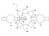
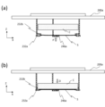
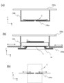
図1は、成膜装置1の構成を模式的に示す平面図である。ここでは、有機ELディスプ
レイの製造ラインについて説明する。有機ELディスプレイを製造する場合、製造ラインに所定のサイズの基板を搬入し、有機ELや金属層の成膜を行った後、基板のカットなどの後処理工程を実施する。
Example 1
(Device configuration)
1 is a plan view showing a schematic configuration of a
成膜装置1は、中央に配置される搬送室130と、搬送室130の周囲に配置される複数の成膜室110(110a~110d)およびマスクストック室120(120a、120b)を含む。成膜室110は、基板10に対する成膜処理が行われるチャンバを備える。マスクストック室120は使用前後のマスクを収納する。搬送室130内に設置された搬送ロボット140は、基板SやマスクMを搬送室130に搬入および搬出する。搬送ロボット140は、例えば、多関節アームに基板SやマスクMを保持するロボットハンドが取り付けられたロボットである。
The
パス室150は、基板搬送方向において上流側から流れてくる基板Sを搬送室130に搬送する。バッファ室160は、搬送室130での成膜処理が完了した基板Sを下流側の他の成膜クラスタに搬送する。搬送ロボット140は、パス室150から基板Sを受け取ると、複数の成膜室110のうちの一つに搬送する。搬送ロボット140はまた、成膜処理が完了した基板Sを成膜室110から受け取り、バッファ室160に搬送する。
The
図1に示す成膜装置1は、1つの成膜クラスタを構成しており、上流側や下流側に別の成膜クラスタを接続することができる。パス室150のさらに上流側や、バッファ室160のさらに下流側には、基板10の方向を変える旋回室170が設けられる。成膜室110、マスクストック室120、搬送室130、バッファ室160、旋回室170などの各チャンバは、製造過程で高真空状態に維持される。
The
成膜装置1の複数の成膜室110a~110dにおける成膜材料は、同じであってもよく、異なっていてもよい。例えば、成膜室110a~110dそれぞれに異なる成膜材料の成膜源を配置し、基板Sが成膜室110a~110dを順に移動しながら積層構造を形成されるようにしてもよい。また、成膜室110a~110dに同じ成膜材料の成膜源を配置することで、複数の基板Sに並行して成膜を行ってもよい。また、成膜室110aと110cに第1の成膜材料を、成膜室110bと110dに第2の成膜材料を配置しておき、成膜室110aまたは110cで第1の層を成膜したのち、成膜室110bまたは110で第2の層を成膜するように制御してもよい。
The film forming materials in the multiple
静電チャックの種類によっては、基板に導電体が付着している場合に基板の吸着力を高めることができる。そのような場合、基板のうち有機EL素子が形成される領域(典型的には基板の中央部)に、電極層となる金属材料の薄膜が既に形成されているときに効果的に吸着できる。例えば、成膜室110aで電極層が成膜された基板上に、成膜室110b~110dで有機層が順次成膜される場合、成膜室110b~110dに静電チャックを配置すると効果的である。
Depending on the type of electrostatic chuck, the force of adhesion of the substrate can be increased when a conductive material is attached to the substrate. In such a case, electrostatic chucks can be effectively attached when a thin film of a metal material that will become an electrode layer has already been formed in the region of the substrate where the organic EL element is to be formed (typically the center of the substrate). For example, when organic layers are sequentially formed in
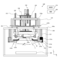
(成膜室)
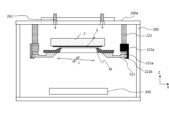
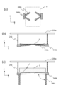
図2は、成膜室110の内部構成を示す断面図である。成膜室110では、搬送ロボット140からの基板SやマスクMの受け取り、搬送ロボット140への基板SやマスクMの受け渡し、静電チャックCによる基板Sの保持、基板SとマスクMの相対的な位置関係を調整するアライメント、マスクMへの基板Sの固定、成膜などの一連の成膜プロセスが行われる。以下の説明においては、鉛直方向をZ方向とするXYZ直交座標系を用い、Z軸まわりの回転をθで表す。なお、左右対称に現れる部材については、簡略化のため符号を左右いずれか一方のみに付す。
(Film forming chamber)
2 is a cross-sectional view showing the internal configuration of the
成膜室110は、チャンバ200を有する。チャンバ200の内部は、成膜の間、真空
雰囲気、または、窒素ガスなどの不活性ガス雰囲気に維持される。チャンバ200の内部には、静電チャックC、複数の基板支持部232a(複数の支持部材)、マスク台221、蒸発源240(成膜源)などが設けられる。以下、基板S、マスクM、静電チャックC、マグネットGを移動させる構成を中心として、チャンバ内部の説明を行う。以下の説明において各部材を昇降させたり移動させたりする機構は、既存の駆動機構、例えばモータの駆動力を用いて動作するボールねじやラックアンドピニオン機構の組み合わせにより実現できるため、詳細な説明を省略する。
The
マスクMは、基板上に形成される薄膜パターンに対応する開口パターンを持つ。マスクMとして例えば、パターンが形成された金属箔の周囲をフレームで支持するメタルマスクを利用できる。マスクMは、チャンバ200内に搬入されるとまず、マスク仮受部224aに載置される。マスク仮受部昇降機構224は、マスク仮受部支持プレート224bを介してチャンバ天井200aに固定されており、マスク仮受部224aを昇降させることができる(図中に矢印Eで示す)。マスク仮受部昇降機構224がマスク仮受部224aを下降させることで、マスク仮受部224aに載置されたマスクMが、マスク台221上に載置される。
The mask M has an opening pattern that corresponds to the thin film pattern formed on the substrate. For example, a metal mask in which a metal foil on which a pattern is formed is supported by a frame can be used as the mask M. When the mask M is brought into the
本実施例のマスク台221は第1磁気発生部221aを有する磁気浮上方式の機構である。また、成膜室110は、チャンバ天井200aに吊り下げ固定される形で、第2磁気発生部222aを有するマスク台支持機構222を備えている。制御部270が第1磁気発生部221aと第2磁気発生部222aに印加される電圧を制御することで、電磁気力によりマスク台221が磁気浮上する。その浮上状態で磁力によりXY移動およびθ回転を行うことが可能である(図中に十字形の矢印Lで示す)。なおマスク台支持機構222は更に、マスク台221が浮上していないときに当該マスク台221を支持するマスク台支持部222bを有している。ただし、マスクを支持および移動させるための機構は、磁力を用いる方式には限定されない。また、磁力を用いる方式においても、マスク台221が浮上する方式には限定されない。例えば、ベアリング等によりマスク台221が転がり移動する方式において、移動に磁力を用いるようにしてもよい。
In this embodiment, the mask table 221 is a magnetic levitation mechanism having a first
基板Sは、チャンバ200内に搬入されると、受け爪状の複数の基板支持部232aにより指示される。基板支持部昇降機構232は、駆動機構によって基板支持部232aを昇降させることにより、基板SのZ方向(基板面に垂直な方向)での高さを変えることができる(図中に矢印Fで示す)。本実施例の基板Sは略水平に配置され、被成膜面は下方を向いており、下方から放出された蒸発材料が付着する、デポアップ方式を採用する。
When the substrate S is loaded into the
ここでチャンバ200の上方において、チャンバ天井200aにはベース部238が固定されている。チャンバ200の上方にはまた、ベース部238に対して昇降可能に取り付けられた昇降プレート230が設けられている。すなわち昇降プレート230は、チャンバ天井200aと平行を保ちながらZ方向で上下動可能である。この昇降プレート230には、静電チャック支持軸230aを介して静電チャックCが設置されているとともに、基板支持部昇降機構232が設置されている。すなわち、昇降プレートが上下動することにより、静電チャックCと基板支持部232aが相対的な位置関係を変えないまま、共に移動することが可能である。
Here, above the
さらに本実施例では、昇降プレート230に、軸等の押上部材支持部246を介して、押上部材246aが接続されている。成膜室には、押上部材246aを、基板Sの被成膜面の中央部に対向する位置である押上位置と、基板に対向する領域から外れた退避位置の間で移動させるための退避機構を備えることが好ましい。押上部材246aは金属、樹脂、ゴムなど任意の材料で構成できるが、少なくとも当接部においては、基板Sの荷重を受けたときでも表面を傷つけないような材料を用いることが好ましい。なお、基板Sの被成
膜面の中央部とは、少なくとも、基板支持部232aや基板当接部232bによってクランプされる周縁部とは異なる領域であり、被押上部と呼ぶこともできる。中央部は典型的には、周縁部よりも内側の領域である。なお、クランプされていない領域であれば、基板Sの端部であっても押上部材246aが当接することが可能であり、例えば後述する図8(b)において押上部材246aに対向している領域を被押上部と呼ぶことができる。
Further, in this embodiment, the
昇降プレート230がZ方向に移動することに伴い、押上部材246aも移動する。あるいは、押上部材支持部246が押上部材246aを上下動させるための駆動機構を有していてもよい。駆動機構が動作することにより押上部材246aが移動し(図中に矢印Pで示す)、基板Sに当接すると、基板Sの荷重を支持することができる。
As the
また基板支持部昇降機構232において、複数の基板支持部232aにそれぞれ対向する位置には、複数の基板当接部232b(複数の当接部材)が設けられている。基板支持部232aに基板Sが載置された状態で制御部270が基板当接部232bを下降させることで、基板Sを基板支持部232aと基板当接部232bの間にクランプすることができる。クランプの際は基板Sを完全に固定することもできるし、ある程度の隙間を持って挟持することで、基板Sを所定の規制範囲内で移動可能としてもよい。
Furthermore, in the substrate support
静電チャックCは、成膜室内部における基板Sの吸着部材であり、基板支持部232aに支持された基板Sを静電気力により吸着保持する。静電チャックCは、基板SのマスクMと接触する面(第1の面、被成膜面)とは反対側の面(第2の面)に当接する。上述したように、昇降プレート230のZ方向の移動に伴って静電チャックCも移動する。静電チャックCが基板支持部232aに支持された基板Sを保持する際には、まず基板支持部昇降機構232が基板Sを上昇させる、及び/又は、昇降プレート230が静電チャックCを下降させて、静電チャックCを基板Sに当接または十分に接近させる。そして、制御部270が電源290を制御して、静電チャックCに埋設された電極に所定の吸着電圧を印加する。すると静電気力が発生し、静電チャックCが基板Sを吸着し保持する。
The electrostatic chuck C is an adsorption member for the substrate S inside the film formation chamber, and adsorbs and holds the substrate S supported by the
静電チャックCのZ方向の上部には、マスクMを引きつけるためのマグネットGが配置されている。マグネットGは、ベース部238に設置されたマグネット昇降機構244と軸を介して接続されている。マグネット昇降機構244が駆動装置を動作させることでマグネットGの磁力が静電チャックCおよび基板Sを介してマスクMに影響を及ぼし、マスクMが上方に引き寄せられる。これによりマスクMと基板Sの密着度が高まり、成膜の精度が向上する。なお、静電チャックCの内部または上部や、マグネットGの内部または上部に、成膜時の基板Sの温度上昇を抑えて有機材料の変質や劣化を防ぐための冷却部材を設けることが好ましい。
A magnet G is disposed above the electrostatic chuck C in the Z direction to attract the mask M. The magnet G is connected to a
蒸発源240は、蒸着材料を収容するルツボ等の容器、ヒータ、シャッタ、駆動機構、蒸発レートモニタなどを含む成膜源である。蒸着材料としては金属材料や有機材料など、所望の膜を形成するのに必要なものを利用できる。なお、成膜源は蒸発源には限られず、スパッタリング装置を用いてもよい。
The
このように本実施例の構成では、基板S、マスクMおよび静電チャックCをそれぞれ駆動することで、基板S、マスクMおよび静電チャックCの位置、高さおよび相対距離の調整が可能である。これに、制御部270による電位制御を組み合わせることにより、静電チャックCやマグネットGによる基板SやマスクMの保持、基板SとマスクMの相対的な位置調整(アライメント)など、成膜に必要な各種の動作を実行できる。なお、これらの動作を実行可能であれば本実施例の構成には限定されない。例えば基板SとマスクMのアライメント手段は、基板SとマスクMのどちらを移動させてもよいし、両方を移動させてもよい。またZ方向の移動についても、基板S、マスクM、静電チャックCのいずれを動
かしてもよい。
In this manner, in the configuration of this embodiment, the positions, heights, and relative distances of the substrate S, mask M, and electrostatic chuck C can be adjusted by driving the substrate S, mask M, and electrostatic chuck C, respectively. By combining this with potential control by the
チャンバ200の上部には、光学撮像を行って画像データを生成するカメラ261が設けられている。カメラ261は、チャンバ200に設けられた真空用の封止窓を通して撮像を行う。本実施例では基板Sの四隅に対応するように、複数(4台)のカメラ261が設けられている。それぞれのカメラ261は、撮像範囲に、基板Sの隅部に設けられた基板アライメントマークと、マスクMの隅部に設けられたマスクアライメントマークが含まれるように配置される。
A
アライメント時には、カメラ261は、基板SおよびマスクMを撮像して画像データを制御部270に出力する。制御部270は画像データを解析し、パターンマッチング処理などの手法により、基板アライメントマークとマスクアライメントマークの位置情報を取得する。そして、基板アライメントマークとマスクアライメントマークの位置ずれ量に基づき、基板SとマスクMを相対的に移動させるときのXY方向、移動距離、回転角度θを算出する。そして、算出された移動量を、各駆動機構の駆動量に変換し、制御信号を生成する。なお、低解像だが広視野のラフアライメント用のカメラと、狭視野だが高解像のファインアライメント用のカメラを用いて、二段階アライメントを行ってもよい。
During alignment, the
制御部270は、不図示の制御線や無線通信を介して各構成要素との間で通信を行い、データを受信したり、信号を送って動作を制御したりする、情報処理装置である。制御部270は、例えば、プロセッサ、メモリ、ストレージ、I/Oなどを有するコンピュータにより構成可能である。この場合、制御部270の機能は、メモリ又はストレージに記憶されたプログラムをプロセッサが実行することにより実現される。コンピュータとしては、汎用のパーソナルコンピュータを用いてもよいし、組込型のコンピュータ又はPLC(programmable logic controller)を用いてもよい。あるいは、制御部270の機能の一部又は全部をASICやFPGAのような回路で構成してもよい。なお、成膜室ごとに制御部270が設けられていてもよいし、1つの制御部270が複数の成膜室を制御してもよい。
The
電源290は、不図示の導電線を介して各構成要素に電圧を供給する高圧電源装置である。電源290は、制御部270からの指令に従って印加電圧の極性や大きさを制御する。静電チャックCの電極に対する印加電圧(吸着電圧)の極性や大きさを制御することで、基板Sに対する吸着力を制御することができる。また、第1磁気発生部221aと第2磁気発生部222aに印加される電圧を制御することで、マスク台221の浮上やアライメント制御を行うことができる。なお、電源290と制御部270を合わせて、成膜装置の電源を構成すると考えてもよい。
The
なお、本発明の適用対象は、上述のようなクラスタ型の成膜装置に限定されない。本発明は、複数のチャンバが真空一貫に連結され、基板キャリアに保持された基板がチャンバ間を移動しながら成膜されるようなインライン型の成膜装置にも適用できる。 The application of the present invention is not limited to the cluster-type deposition apparatus described above. The present invention can also be applied to an in-line deposition apparatus in which multiple chambers are connected through a vacuum, and a substrate held by a substrate carrier is moved between the chambers while a film is deposited thereon.
(静電チャック)
静電チャックCは、セラミック等で構成された板状の基材に、金属電極などの電気回路が埋設された構造を有する。一般に静電チャックには、基板を吸着する原理に応じて、グラディエント力タイプ、クーロン力タイプ、ジョンソン・ラーベック力タイプなどの種類があるが、いずれにおいても印加する吸着電圧を高めるほど吸着力を高くすることができる。静電チャックCの製造方法の一例は、チタン母材および絶縁層からなるセラミック溶射層に、電極を配置し、誘電層を形成した後、最後にセラミック溶射で封をする方法である。
(Electrostatic chuck)
The electrostatic chuck C has a structure in which an electric circuit such as a metal electrode is embedded in a plate-shaped base material made of ceramic or the like. Generally, electrostatic chucks are classified into types such as gradient force type, Coulomb force type, and Johnsen-Rahbek force type according to the principle of attracting a substrate, and in any case, the attracting force can be increased by increasing the attracting voltage applied. One example of a method for manufacturing the electrostatic chuck C is a method in which electrodes are arranged on a ceramic sprayed layer made of a titanium base material and an insulating layer, a dielectric layer is formed, and then finally, sealing is performed by ceramic spraying.
グラディエント力タイプの静電チャックは、電極間の電位差により発生した電位勾配(グラディエント)のある領域に向かって生じる吸引力を利用して、吸着対象物を吸着する。グラディエント力は、吸着対象物が絶縁体であっても発生するという特徴があるため、素ガラスや、導電体が未成膜のガラス基板であっても保持可能である。グラディエント力を発生させる際は、吸着対象物の電位を基準として、第1電極の電位が基準より高くなり、第2電極の電位が基準より低くなるように吸着電圧を印加する。このグラディエント力を大きくするためには、電位勾配をできるだけ急峻にするために、電極間のスペースを小さくすることと、電極を緻密に配置することが必要である。したがってグラディエント力タイプの静電チャックに用いる電極としては、突出した櫛歯が互いに噛み合うような構造を持つ、2つの櫛歯電極が好適である。 Gradient force type electrostatic chucks attract objects by utilizing the attraction force that occurs toward an area with a potential gradient (gradient) generated by the potential difference between the electrodes. The gradient force is generated even if the object to be attracted is an insulator, so it can hold even plain glass or a glass substrate with no conductor formed thereon. When generating the gradient force, an attraction voltage is applied so that the potential of the first electrode is higher than the reference potential of the object to be attracted and the potential of the second electrode is lower than the reference potential, based on the potential of the object to be attracted. In order to increase this gradient force, it is necessary to reduce the space between the electrodes and to arrange the electrodes closely together in order to make the potential gradient as steep as possible. Therefore, two comb-tooth electrodes with a structure in which the protruding comb teeth interdigitate with each other are suitable as electrodes to be used in gradient force type electrostatic chucks.
クーロン力タイプの静電チャックは、2つの電極にそれぞれ正電位と負電位の電圧を印加することで発生する静電引力により吸着対象物を吸着するものであり、吸着対象物が導電体である場合に効果的である。そのため、金属材料の電極層が成膜済みの基板であれば効果的に吸着できる。吸着対象物がグランドに接続されていないフローティング状態の場合は、正電極と負電極の両方を吸着対象物に対向させることで、吸着対象物内に分極を発生させ、吸着することができる。また吸着対象物が接地されている場合は、正電極と負電極の少なくともいずれかにより吸着することができる。クーロン力は一般にグラディエント力よりも強い。また、吸着対象物に対向する電極の面積が大きくなるほど、吸着力が強くなる。したがって吸着力を高めるためには、静電チャックの面積に占める電極面積の割合をできるだけ大きくする必要がある。 The Coulomb force type electrostatic chuck attracts an object to be attracted by electrostatic attraction generated by applying a positive potential voltage and a negative potential voltage to two electrodes, respectively, and is effective when the object to be attracted is a conductor. Therefore, it can be effectively attracted to a substrate on which an electrode layer of a metal material has already been formed. When the object to be attracted is in a floating state not connected to ground, it is possible to attract the object by generating polarization in the object to be attracted by facing both the positive and negative electrodes. When the object to be attracted is grounded, it can be attracted by at least one of the positive and negative electrodes. Coulomb force is generally stronger than gradient force. Also, the larger the area of the electrode facing the object to be attracted, the stronger the attraction force. Therefore, in order to increase the attraction force, it is necessary to increase the ratio of the electrode area to the area of the electrostatic chuck as much as possible.
ジョンソン・ラーベック力タイプの静電チャックは、正電極、吸着対象物、負電極の順に漏れ電流を流すことで、導電体の吸着対象物を吸着するものであり、電極と吸着対象物の間に所定の範囲の体積抵抗値を持つ誘電体を配置する必要がある。ジョンソン・ラーベック力は一般にクーロン力よりも強い。またジョンソン・ラーベック力タイプの静電チャックにおいても、吸着対象物との接触面積を大きくするほど吸着力を強くすることができる。 Johnson-Rahbek force type electrostatic chucks attract conductive objects by passing a leakage current through the positive electrode, the object to be attracted, and the negative electrode in that order, and require a dielectric with a volume resistance value within a specified range to be placed between the electrode and the object to be attracted. The Johnson-Rahbek force is generally stronger than the Coulomb force. Also, with the Johnson-Rahbek force type electrostatic chuck, the greater the contact area with the object to be attracted, the stronger the chucking force can be.
(処理フロー)
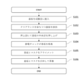
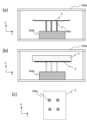
図3のフローチャートを参照しつつ、本実施例における基板Sの吸着方法を含む処理について説明する。図4~図7は、処理中の成膜室110のチャンバ200内の様子を示す模式的な断面図であり、当該ステップにおける説明に関係のない部分は省略している。
(Processing flow)
The process including the method for adsorbing the substrate S in this embodiment will be described with reference to the flow chart of Fig. 3. Figs. 4 to 7 are schematic cross-sectional views showing the state inside the
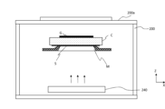
本フローは、搬送ロボット140により基板Sが成膜室110に搬入された時点からスタートする。ステップS101において、図4(a)に示すように、基板支持部232aが、搬入された基板Sを受け取って支持する。基板Sの大きさにもよるが、端部を支持された基板Sの中央部は自重により撓んで垂下する。
This flow starts when the substrate S is carried into the
ステップS102において、図4(b)に示すように、基板当接部232bが下降することにより、基板支持部232aとの間で基板Sの端部を挟持する(矢印S)。このときの基板支持部232aと基板当接部232bの間のZ方向での距離Rは、基板Sの厚さよりも長いものとする。すなわち、基板支持部232aと基板当接部232b(2つを合わせてクランプ部とも呼ぶ)は、基板Sを完全に固定するのではなく、ある程度のクリアランス幅を持って挟持している。これにより、基板SのZ方向における動きを一定の範囲内に規制しつつ、基板SがXY平面内において動くことを可能としている。
In step S102, as shown in FIG. 4(b), the
ステップS103において、図5(a)に示すように、押上部材支持部246が押上部材246aを上昇させて、基板Sの中央部を押し上げる(矢印P)。これにより基板Sの撓みが軽減されて平坦度が向上する。このとき、上述したZ方向におけるクリアランスが
あることによって、基板Sの端部が、基板支持部232aと基板当接部232bの間の位置を保ちつつ、基板Sの周縁方向に伸張する。そのため、押し上げの際に基板S中央部の撓みが伝播することないので、基板Sが波打ったり跳ね上がったりすることがなくなり、平坦な形状となる。
5A, in step S103, the boost
ステップS104において、図5(a)に示すように、静電チャックCが基板Sを吸着する。このとき、昇降プレート230の駆動により静電チャックCが下降し、静電チャックCと基板Sの相対的な距離が十分に接近したときに制御部270が電源290を制御して、静電チャックCに吸着電圧を印加する。これにより発生した静電気力によって、静電チャックCが基板Sを吸着し保持する。基板Sが保持されたあとは、必ずしも基板をクランプする必要はないため、基板支持部232a、基板当接部232b、押上部材246aなどは退避させてよい。
In step S104, as shown in FIG. 5(a), the electrostatic chuck C attracts the substrate S. At this time, the
ステップS105において、図6に示すように、基板SとマスクMのアライメントが行われる。このとき、マスク台221上のマスクMと、基板Sとの間でZ方向における所定のアライメント距離を保ちつつ、マスク台221の第1磁気発生部221aとマスク台支持機構222の第2磁気発生部222aの間の電磁気力により浮上した状態となっている。そして、制御部270は、カメラ261により撮像された基板四隅の基板アライメントマークとマスク四隅のマスクアライメントマークが所定の位置関係となるように、第1磁気発生部221aと第2磁気発生部222aに印加する電圧を制御して、マスク台221をXY移動およびθ回転させる。
In step S105, as shown in FIG. 6, the substrate S and the mask M are aligned. At this time, the mask M on the mask table 221 is in a levitated state due to the electromagnetic force between the first magnetic
アライメントが完了すると、ステップS106において、図7に示すように、制御部270は、マスク台221を上昇させてマスクMと基板Sを当接させる。また、マグネットGを下降させて、磁力によりマスクMを上方に引き付ける。これにより基板SとマスクMの合体が完了する。そして制御部270は、蒸発源240のヒータに電流を流すことで坩堝内を高温とし、蒸発材料を気化させる。これにより、基板Sの被成膜面に向かって蒸発材料が飛翔し、マスクMの所定のパターンに応じた薄膜が形成される。
When the alignment is complete, in step S106, as shown in FIG. 7, the
以上のフローに示す方法によれば、静電チャックCが基板Sを吸着するときに、基板Sの中央部が押し上げられていることで、撓みが低減され平坦度が向上した状態となっている。そのため、比較的大型の基板であっても、静電チャックCによる吸着の際に波打ちや跳ね上がりが抑制され、吸着後の基板の剥離や落下を防ぐことが可能となる。 According to the method shown in the flow chart above, when the electrostatic chuck C attracts the substrate S, the center of the substrate S is pushed up, reducing bending and improving flatness. Therefore, even for relatively large substrates, rippling and bouncing are suppressed when the substrate is attracted by the electrostatic chuck C, and it is possible to prevent the substrate from peeling off or falling off after attraction.
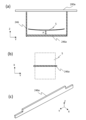
(押上部材)
以下、本実施例に適用可能な押上部材246aの種々の例について説明する。押上部材246aは、基板Sが基板支持部232aにより支持されてから静電チャックCに吸着されるまでの間、基板Sを重力と反対方向に押し上げる機能があればよく、形状や材質は問わない。また、アライメントや蒸着の際に押上部材246aが妨げとならないように、静電チャックCによる基板Sの吸着後は、押上部材246aを基板に対向する位置から退避させるための構成を設けることが好ましい。ただし、アライメントや蒸着などの妨げにならないのであれば、必ずしも退避機構は必要ない。
(Lifting member)
Various examples of the push-up
図8は、バー形状の押上部材246aを説明するための図である。図8(a)は、図2のXZ断面とは異なるYZ断面図である。押上部材246aが上方向に駆動されることにより、基板Sの中央部が押し上げられる。図8(b)はXY平面図であり、基板Sと押上部材246aの平面的な位置関係を示している。図8(c)はバー形状の押上部材246aの形状の例であり、端部は駆動機構に接続され、中央部は基板Sに接触する。本図の押上部材246aは、上面が略長方形をしており、上面の各辺が基板Sの被成膜面に線接触することにより基板Sの荷重を支える。ただし基板Sを支持する構成はこれに限定されず
、例えば上面の面接触で支持してもよいし、上面に樹脂やゴムなどのクッション性のある部材を配してもよい。また、バー形状の押上部材246aとして、金属材料等で形成されたワイヤー状の部材に張力をかけて用いても良い。
FIG. 8 is a diagram for explaining the bar-shaped push-up
なお、図8では1箇所だけに押上部材246aが設けられていたが、数は1個に限定されず、基板Sの大きさに応じた個数の押上部材246aを設けてもよい。例えば平行に3本のバー形状の押上部材246aを設けることができる。
In FIG. 8, a push-up
図9は、バー形状の押上部材246aの別例を説明するための図である。図9(a)に示すように、この例の押上部材246aは2つの部分に分かれており、同期してZ方向に上下移動を行う。図9(b)、図9(c)に示すように、アライメントや蒸着を行うときには、左右それぞれの押上部材246aが基板Sに対向する押上位置からスライドして、退避位置に移動することが可能である。このような構成によっても基板Sを安定して吸着する効果が得られるとともに、押し上げを行わないときの退避が容易になる。
Figure 9 is a diagram illustrating another example of a bar-shaped push-up
なお、図9の例では押上部材246aが1組だけ設けられていたが、基板Sの大きさに応じた個数の押上部材246aを設けてもよい。例えば平行に3組のバー形状の押上部材246aを設けることができる。
In the example of FIG. 9, only one set of
図10は、片持ち梁形状で被支持端が回動するタイプの押上部材246aの例を示す。図10(a)のYX平面図と、図10(b)のXZ平面での断面図に示すように、押上部材246aは、支持基部246bにより固定端を片持ち支持されながら、自由端により基板Sを押し上げる。そして静電チャックCにより基板Sが吸着され保持された後は、図10(c)に示すように、支持基部246bが備える駆動機構によって固定端の固定角度が変更され、退避位置に移動することが可能である。
Figure 10 shows an example of a push-up
図11は、Z方向に上下動するピン形状の押上部材246aの例を示す。図11(a)のXZ平面での断面図に示すように、押上部材246aは、一端を支持基部246bにより支持されながら、他端により基板Sを押し上げる。そして静電チャックCにより基板Sが吸着され保持された後は、図11(b)に示すように、支持基部246bが備える駆動機構によって押上部材246aが下方の退避位置に移動することが可能である。図11(c)では、基板Sの被成膜面におけるピンの端部による押し上げ位置の例を示したが、これには限定されない。
Figure 11 shows an example of a pin-shaped push-up
以上述べたように、本発明によれば、押上部材246aが基板の中央部を押し上げることにより基板Sの撓みが低減される。また基板Sの端部は完全に固定されているわけではなく基板Sが伸張できる程度に軽くクランプされた状態であるため、基板Sの撓みは端部に追いやられて吸収される。このような状態で静電チャックCが基板Sを吸着することにより、吸着時の波打ちや跳ね上がりが抑制されて安定的な基板保持が可能となる。よって、吸着後の基板の剥離や落下を防ぐことが可能となる。
As described above, according to the present invention, the push-up
<電子デバイスの製造方法>
次に、本実施例の成膜装置を用いた電子デバイスの製造方法の一例を説明する。以下、電子デバイスの例として有機EL表示装置の構成を示し、有機EL表示装置の製造方法を例示する。
<Method of Manufacturing Electronic Device>
Next, an example of a method for manufacturing an electronic device using the film forming apparatus of this embodiment will be described below. The configuration of an organic EL display device will be shown as an example of an electronic device, and a method for manufacturing the organic EL display device will be illustrated.
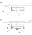
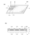
まず、製造する有機EL表示装置について説明する。図12(a)は有機EL表示装置180の全体図、図12(b)は1画素の断面構造を表している。
First, the organic EL display device to be manufactured will be described. Figure 12(a) shows an overall view of the organic
図12(a)に示すように、有機EL表示装置180の表示領域151には、発光素子
を複数備える画素152がマトリクス状に複数配置されている。詳細は後で説明するが、発光素子のそれぞれは、一対の電極に挟まれた有機層を備えた構造を有している。なお、ここでいう画素とは、表示領域151において所望の色の表示を可能とする最小単位を指している。本実施例に係る有機EL表示装置の場合、互いに異なる発光を示す第1発光素子152R、第2発光素子152G、第3発光素子152Bの組み合わせにより画素152が構成されている。画素152は、赤色発光素子と緑色発光素子と青色発光素子の組み合わせで構成されることが多いが、黄色発光素子とシアン発光素子と白色発光素子の組み合わせでもよく、少なくとも1色以上であれば特に制限されるものではない。
As shown in FIG. 12A, a plurality of
図12(b)は、図12(a)のA-B線における部分断面模式図である。画素152は、複数の発光素子からなり、各発光素子は、基板153上に、第1電極(陽極)154と、正孔輸送層155と、発光層156R、156G、156Bのいずれかと、電子輸送層157と、第2電極(陰極)158と、を有している。これらのうち、正孔輸送層155、発光層156R、156G、156B、電子輸送層157が有機層に当たる。また、本実施例では、発光層156Rは赤色を発する有機EL層、発光層156Gは緑色を発する有機EL層、発光層156Bは青色を発する有機EL層である。発光層156R、156G、156Bは、それぞれ赤色、緑色、青色を発する発光素子(有機EL素子と記述する場合もある)に対応するパターンに形成されている。また、第1電極154は、発光素子毎に分離して形成されている。正孔輸送層155と電子輸送層157と第2電極158は、複数の発光素子152R、152G、152Bで共通に形成されていてもよいし、発光素子毎に形成されていてもよい。なお、第1電極154と第2電極158とが異物によってショートするのを防ぐために、第1電極154間に絶縁層159が設けられている。さらに、有機EL層は水分や酸素によって劣化するため、水分や酸素から有機EL素子を保護するための保護層145が設けられている。
Figure 12 (b) is a partial cross-sectional schematic diagram taken along line A-B in Figure 12 (a).
図12(b)では正孔輸送層155や電子輸送層157は一つの層で示されているが、有機EL表示素子の構造によっては、正孔ブロック層や電子ブロック層を備える複数の層で形成されてもよい。また、第1電極154と正孔輸送層155との間には第1電極154から正孔輸送層155への正孔の注入が円滑に行われるようにすることのできるエネルギーバンド構造を有する正孔注入層を形成することもできる。同様に、第2電極158と電子輸送層157の間にも電子注入層が形成することもできる。
In FIG. 12(b), the
次に、有機EL表示装置の製造方法の例について具体的に説明する。 Next, we will explain in detail an example of a manufacturing method for an organic EL display device.
まず、有機EL表示装置を駆動するための回路(不図示)及び第1電極154が形成された基板153を準備する。
First, a circuit (not shown) for driving the organic EL display device and a
第1電極154が形成された基板153の上にアクリル樹脂をスピンコートで形成し、アクリル樹脂をリソグラフィ法により、第1電極154が形成された部分に開口が形成されるようにパターニングし絶縁層159を形成する。この開口部が、発光素子が実際に発光する発光領域に相当する。
An acrylic resin is formed by spin coating on the
絶縁層159がパターニングされた基板153を第1の有機材料成膜装置に搬入し、基板支持台及び静電チャックにて基板を保持し、正孔輸送層155を、表示領域の第1電極154の上に共通する層として成膜する。正孔輸送層155は真空蒸着により成膜される。実際には正孔輸送層155は表示領域151よりも大きなサイズに形成されるため、高精細なマスクは不要である。
The
次に、正孔輸送層155までが形成された基板153を第2の有機材料成膜装置に搬入し、基板支持台及び静電チャックで保持する。基板とマスクとのアライメントを行い、基
板をマスクの上に載置し、基板153の赤色を発する素子を配置する部分に、赤色を発する発光層156Rを成膜する。
Next, the
発光層156Rの成膜と同様に、第3の有機材料成膜装置により緑色を発する発光層156Gを成膜し、さらに第4の有機材料成膜装置により青色を発する発光層156Bを成膜する。発光層156R、156G、156Bの成膜が完了した後、第5の成膜装置により表示領域151の全体に電子輸送層157を成膜する。電子輸送層157は、3色の発光層156R、156G、156Bに共通の層として形成される。
Similar to the deposition of the light-emitting
電子輸送層157まで形成された基板を金属性蒸着材料成膜装置で移動させて第2電極158を成膜する。
The substrate on which the
その後プラズマCVD装置に移動して保護層145を成膜して、有機EL表示装置180が完成する。
Then, it is moved to a plasma CVD device to deposit a
絶縁層159がパターニングされた基板153を成膜装置に搬入してから保護層145の成膜が完了するまでは、水分や酸素を含む雰囲気にさらしてしまうと、有機EL材料からなる発光層が水分や酸素によって劣化してしまうおそれがある。従って、本実施例において、成膜装置間の基板の搬入搬出は、真空雰囲気又は不活性ガス雰囲気の下で行われる。
If the
1:成膜装置、232a:基板支持部、232b:基板当接部、246a:押上部、C:静電チャック、S:基板 1: Film forming device, 232a: Substrate support part, 232b: Substrate contact part, 246a: Push-up part, C: Electrostatic chuck, S: Substrate
Claims (15)
前記基板において成膜が行われる第1の面の周縁部を支持する複数の支持部材と、
前記複数の支持部材とそれぞれ対向する複数の当接部材であって、前記基板の前記第1の面とは反対の第2の面に当接する、複数の当接部材と、
前記基板の前記第1の面が前記複数の支持部材に支持され、前記複数の当接部材が前記第2の面に当接している状態で、前記基板の前記第1の面のうち、前記周縁部よりも内側の領域を押し上げる押上部材と、
前記基板の前記内側の領域が押し上げられた状態で、前記基板の前記第2の面を吸着する吸着部材と、
を備えることを特徴とする成膜装置。 A film forming apparatus for depositing a film forming material onto a substrate, comprising:
A plurality of support members for supporting a peripheral portion of a first surface of the substrate on which a film is formed;
a plurality of abutment members facing the plurality of support members, respectively, and abutting a second surface of the substrate opposite the first surface;
a push-up member that pushes up an area of the first surface of the substrate that is located inside the peripheral portion while the first surface of the substrate is supported by the plurality of support members and the plurality of abutment members are in contact with the second surface;
a suction member that suctions the second surface of the substrate while the inner region of the substrate is pushed up;
A film forming apparatus comprising:
前記基板は、前記第1の面が下方を向いた状態で成膜が行われる
ことを特徴とする請求項1に記載の成膜装置。 a deposition source that emits the deposition material from below the substrate;
2. The film forming apparatus according to claim 1, wherein the film is formed on the substrate with the first surface facing downward.
ことを特徴とする請求項1に記載の成膜装置。 2. The film deposition apparatus according to claim 1, wherein a distance between the support member and the contact member in a direction perpendicular to the substrate is longer than a thickness of the substrate.
ことを特徴とする請求項3に記載の成膜装置。 4. The film forming apparatus according to claim 3, wherein the push-up member pushes up the inner region of the substrate while the substrate is sandwiched between the support member and the contact member with a clearance therebetween.
前記吸着部材に印加する吸着電圧を制御する制御部をさらに備える
ことを特徴とする請求項1から4のいずれか1項に記載の成膜装置。 the attraction member is an electrostatic chuck that attracts and holds the substrate by electrostatic force,
5. The film forming apparatus according to claim 1, further comprising a control unit that controls an attraction voltage applied to the attraction member.
ことを特徴とする請求項5に記載の成膜装置。 6. The film forming apparatus according to claim 5, wherein the control unit applies the attraction voltage in a state in which the attraction member and the substrate are close to each other after the inner region of the substrate is pushed up by the push-up member.
ことを特徴とする請求項1から4のいずれか1項に記載の成膜装置。 5. The film forming apparatus according to claim 1, wherein the film forming apparatus deposits a film material onto the substrate through a mask to form a film having a predetermined pattern.
前記吸着部材および前記基板を介して磁力により前記マスクを引き付けるマグネットをさらに備える
ことを特徴とする請求項7に記載の成膜装置。 the mask is a metal mask,
8. The film forming apparatus according to claim 7, further comprising a magnet that attracts the mask by magnetic force via the attraction member and the substrate.
ことを特徴とする請求項7に記載の成膜装置。 8. The film forming apparatus according to claim 7, further comprising an alignment means for adjusting the relative positions of the substrate and the mask.
ことを特徴とする請求項1から4のいずれか1項に記載の成膜装置。 5. The film forming apparatus according to claim 1, further comprising a retraction mechanism for retracting the push-up member from a region facing the substrate after the suction member has adsorbed the substrate.
ことを特徴とする請求項1から4のいずれか1項に記載の成膜装置。 5. The film forming apparatus according to claim 1, wherein the push-up member is a bar-shaped member.
ことを特徴とする請求項11に記載の成膜装置。 12. The film deposition apparatus according to claim 11, wherein the bar-shaped push-up member is slidable and retractable from a region facing the substrate.
前記支持基部は、前記押上部材を押上位置と退避位置の間で移動させることが可能である
ことを特徴とする請求項1から4のいずれか1項に記載の成膜装置。 the lift-up member has a free end that lifts up the substrate and a fixed end that is fixed to a support base;
5. The film deposition apparatus according to claim 1, wherein the support base is capable of moving the push-up member between a push-up position and a retracted position.
ことを特徴とする請求項1から4のいずれか1項に記載の成膜装置。 5. The film forming apparatus according to claim 1, wherein the push-up member is a pin-shaped member that pushes up the substrate from below.
複数の支持部材によって、前記基板において成膜が行われる第1の面の周縁部を支持する工程と、
前記複数の支持部材とそれぞれ対向する複数の当接部材を、前記基板の前記第1の面とは反対の第2の面に当接させる工程と、
押上部材によって、前記基板の前記第1の面のうち、前記周縁部よりも内側の領域を押し上げる工程と、
吸着部材によって、前記基板の前記第2の面を吸着する工程と、
を有する吸着方法。 1. A method for adsorbing and holding a substrate in a film forming apparatus that deposits a film on a substrate by applying a film forming material thereto, comprising:
supporting a peripheral portion of a first surface of the substrate on which a film is to be formed by a plurality of support members;
abutting a plurality of abutment members, each of which faces the plurality of support members, against a second surface of the substrate opposite the first surface;
a step of pushing up a region of the first surface of the substrate that is located inside the peripheral portion by a push-up member;
adsorbing the second surface of the substrate by an adsorption member;
The adsorption method comprising the steps of:
Priority Applications (3)
| Application Number | Priority Date | Filing Date | Title |
|---|---|---|---|
| JP2023110825A JP2025008564A (en) | 2023-07-05 | 2023-07-05 | Film forming apparatus and adsorption method |
| KR1020240081636A KR20250007418A (en) | 2023-07-05 | 2024-06-24 | Film forming method and absorption menthod |
| CN202410881410.5A CN119265530A (en) | 2023-07-05 | 2024-07-03 | Film forming device and adsorption method |
Applications Claiming Priority (1)
| Application Number | Priority Date | Filing Date | Title |
|---|---|---|---|
| JP2023110825A JP2025008564A (en) | 2023-07-05 | 2023-07-05 | Film forming apparatus and adsorption method |
Publications (1)
| Publication Number | Publication Date |
|---|---|
| JP2025008564A true JP2025008564A (en) | 2025-01-20 |
Family
ID=94123688
Family Applications (1)
| Application Number | Title | Priority Date | Filing Date |
|---|---|---|---|
| JP2023110825A Pending JP2025008564A (en) | 2023-07-05 | 2023-07-05 | Film forming apparatus and adsorption method |
Country Status (3)
| Country | Link |
|---|---|
| JP (1) | JP2025008564A (en) |
| KR (1) | KR20250007418A (en) |
| CN (1) | CN119265530A (en) |
Family Cites Families (1)
| Publication number | Priority date | Publication date | Assignee | Title |
|---|---|---|---|---|
| KR102427017B1 (en) | 2018-02-20 | 2022-07-29 | 엘지전자 주식회사 | Defrosting device |
-
2023
- 2023-07-05 JP JP2023110825A patent/JP2025008564A/en active Pending
-
2024
- 2024-06-24 KR KR1020240081636A patent/KR20250007418A/en active Pending
- 2024-07-03 CN CN202410881410.5A patent/CN119265530A/en active Pending
Also Published As
| Publication number | Publication date |
|---|---|
| CN119265530A (en) | 2025-01-07 |
| KR20250007418A (en) | 2025-01-14 |
Similar Documents
| Publication | Publication Date | Title |
|---|---|---|
| CN109837505B (en) | Film forming apparatus, film forming method, and method for manufacturing organic EL display device | |
| KR101933807B1 (en) | Film forming apparatus and manufacturing method of organic el display apparatus using the same | |
| JP7278541B2 (en) | Electrostatic chuck system, film forming apparatus, adsorption method, film forming method, and electronic device manufacturing method | |
| KR102505832B1 (en) | Adsorption apparatus, position adjusting method, and method for forming film | |
| KR20250159140A (en) | Chucking apparatus, film forming apparatus, chucking method, film forming method and manufacturing method of electronic device | |
| CN112779503A (en) | Film forming apparatus and method for controlling film forming apparatus | |
| CN112680696A (en) | Film forming apparatus, electronic device manufacturing apparatus, film forming method, and electronic device manufacturing method | |
| KR102459872B1 (en) | Electrostatic chuk system, film formation apparatus, suction method, film formation method, and manufacturing method of electronic device | |
| JP2019102802A (en) | Film forming apparatus, film forming method, and manufacturing method of organic el display device using the same | |
| KR102501609B1 (en) | Film forming apparatus, film forming method and manufacturing method of electronic device | |
| JP7262221B2 (en) | Electrostatic chuck system, film forming apparatus, adsorption method, film forming method, and electronic device manufacturing method | |
| JP2025008564A (en) | Film forming apparatus and adsorption method | |
| KR102520050B1 (en) | Suction apparatus, film formation apparatus, suction method, film formation method, and manufacturing method of electronic device | |
| JP7078694B2 (en) | Film forming equipment, film forming method, and manufacturing method of electronic devices | |
| KR102501617B1 (en) | Film forming apparatus, film forming method, and manufacturing method of electronic device | |
| KR102419064B1 (en) | Electrostatic chuk system, film formation apparatus, suction method, film formation method, and manufacturing method of electronic device | |
| KR102430370B1 (en) | Electrostatic chuk system, film formation apparatus, suction method, film formation method, and manufacturing method of electronic device | |
| CN112779504A (en) | Film forming apparatus and film forming method | |
| CN113005398B (en) | Film forming apparatus, film forming method, and method for manufacturing electronic device | |
| KR102481907B1 (en) | Film forming apparatus, film forming method and manufacturinh method of electronic device | |
| CN113005397B (en) | Film forming apparatus, film forming method, and method for manufacturing electronic device | |
| CN113088870B (en) | Film forming device, film forming method, and manufacturing method of electronic device | |
| JP2019117924A (en) | Electrostatic chuck, film forming apparatus, substrate suction method, film forming method, and manufacturing method of electronic device | |
| JP2023105428A (en) | SUBSTRATE HOLDING DEVICE, ELECTROSTATIC CHUCK, AND SUBSTRATE HOLDING METHOD | |
| KR20190070896A (en) | Mask attaching device, film-forming apparatus, film-forming method, and method for manufacturing electronic device |