JP2023110900A - Wide band gap transistor with nanolaminated insulating gate structure and method for manufacturing wide band gap transistor - Google Patents
Wide band gap transistor with nanolaminated insulating gate structure and method for manufacturing wide band gap transistor Download PDFInfo
- Publication number
- JP2023110900A JP2023110900A JP2023010393A JP2023010393A JP2023110900A JP 2023110900 A JP2023110900 A JP 2023110900A JP 2023010393 A JP2023010393 A JP 2023010393A JP 2023010393 A JP2023010393 A JP 2023010393A JP 2023110900 A JP2023110900 A JP 2023110900A
- Authority
- JP
- Japan
- Prior art keywords
- layer
- gate structure
- aluminum
- forming
- insulated gate
- Prior art date
- Legal status (The legal status is an assumption and is not a legal conclusion. Google has not performed a legal analysis and makes no representation as to the accuracy of the status listed.)
- Pending
Links
- 238000000034 method Methods 0.000 title claims abstract description 38
- 238000004519 manufacturing process Methods 0.000 title claims abstract description 14
- 239000004065 semiconductor Substances 0.000 claims abstract description 48
- JMASRVWKEDWRBT-UHFFFAOYSA-N Gallium nitride Chemical compound [Ga]#N JMASRVWKEDWRBT-UHFFFAOYSA-N 0.000 claims abstract description 16
- HBMJWWWQQXIZIP-UHFFFAOYSA-N silicon carbide Chemical compound [Si+]#[C-] HBMJWWWQQXIZIP-UHFFFAOYSA-N 0.000 claims abstract description 15
- 229910052782 aluminium Inorganic materials 0.000 claims abstract description 11
- XAGFODPZIPBFFR-UHFFFAOYSA-N aluminium Chemical compound [Al] XAGFODPZIPBFFR-UHFFFAOYSA-N 0.000 claims abstract description 11
- 239000000203 mixture Substances 0.000 claims abstract description 11
- 229910052735 hafnium Inorganic materials 0.000 claims abstract description 9
- VBJZVLUMGGDVMO-UHFFFAOYSA-N hafnium atom Chemical compound [Hf] VBJZVLUMGGDVMO-UHFFFAOYSA-N 0.000 claims abstract description 9
- QVGXLLKOCUKJST-UHFFFAOYSA-N atomic oxygen Chemical compound [O] QVGXLLKOCUKJST-UHFFFAOYSA-N 0.000 claims abstract description 8
- 229910052760 oxygen Inorganic materials 0.000 claims abstract description 8
- 239000001301 oxygen Substances 0.000 claims abstract description 8
- 238000000137 annealing Methods 0.000 claims description 30
- TWNQGVIAIRXVLR-UHFFFAOYSA-N oxo(oxoalumanyloxy)alumane Chemical compound O=[Al]O[Al]=O TWNQGVIAIRXVLR-UHFFFAOYSA-N 0.000 claims description 26
- 229910000449 hafnium oxide Inorganic materials 0.000 claims description 23
- WIHZLLGSGQNAGK-UHFFFAOYSA-N hafnium(4+);oxygen(2-) Chemical compound [O-2].[O-2].[Hf+4] WIHZLLGSGQNAGK-UHFFFAOYSA-N 0.000 claims description 23
- 230000004888 barrier function Effects 0.000 claims description 18
- 238000000151 deposition Methods 0.000 claims description 16
- 239000000463 material Substances 0.000 claims description 15
- 239000000758 substrate Substances 0.000 claims description 12
- 229910002601 GaN Inorganic materials 0.000 claims description 11
- 238000000231 atomic layer deposition Methods 0.000 claims description 9
- 238000002425 crystallisation Methods 0.000 claims description 6
- 230000008025 crystallization Effects 0.000 claims description 6
- RNQKDQAVIXDKAG-UHFFFAOYSA-N aluminum gallium Chemical compound [Al].[Ga] RNQKDQAVIXDKAG-UHFFFAOYSA-N 0.000 claims description 5
- GYHNNYVSQQEPJS-UHFFFAOYSA-N Gallium Chemical compound [Ga] GYHNNYVSQQEPJS-UHFFFAOYSA-N 0.000 claims description 3
- 229910052733 gallium Inorganic materials 0.000 claims description 3
- CJNBYAVZURUTKZ-UHFFFAOYSA-N hafnium(iv) oxide Chemical compound O=[Hf]=O CJNBYAVZURUTKZ-UHFFFAOYSA-N 0.000 claims description 2
- 238000010438 heat treatment Methods 0.000 claims description 2
- 238000007254 oxidation reaction Methods 0.000 claims description 2
- 229910002059 quaternary alloy Inorganic materials 0.000 claims description 2
- 230000003647 oxidation Effects 0.000 claims 1
- 229910002058 ternary alloy Inorganic materials 0.000 claims 1
- 239000010410 layer Substances 0.000 description 105
- 230000008569 process Effects 0.000 description 26
- 230000008021 deposition Effects 0.000 description 13
- 229910052751 metal Inorganic materials 0.000 description 9
- 239000002184 metal Substances 0.000 description 9
- 230000015572 biosynthetic process Effects 0.000 description 6
- 238000000206 photolithography Methods 0.000 description 6
- 239000003989 dielectric material Substances 0.000 description 3
- 229910010271 silicon carbide Inorganic materials 0.000 description 3
- VYPSYNLAJGMNEJ-UHFFFAOYSA-N Silicium dioxide Chemical compound O=[Si]=O VYPSYNLAJGMNEJ-UHFFFAOYSA-N 0.000 description 2
- XUIMIQQOPSSXEZ-UHFFFAOYSA-N Silicon Chemical compound [Si] XUIMIQQOPSSXEZ-UHFFFAOYSA-N 0.000 description 2
- 230000008901 benefit Effects 0.000 description 2
- 238000009792 diffusion process Methods 0.000 description 2
- 230000005684 electric field Effects 0.000 description 2
- 238000005468 ion implantation Methods 0.000 description 2
- 238000012986 modification Methods 0.000 description 2
- 230000004048 modification Effects 0.000 description 2
- 229910052710 silicon Inorganic materials 0.000 description 2
- 239000010703 silicon Substances 0.000 description 2
- 229910052814 silicon oxide Inorganic materials 0.000 description 2
- 229910002704 AlGaN Inorganic materials 0.000 description 1
- 230000004913 activation Effects 0.000 description 1
- 229910045601 alloy Inorganic materials 0.000 description 1
- 239000000956 alloy Substances 0.000 description 1
- 230000009286 beneficial effect Effects 0.000 description 1
- 230000015556 catabolic process Effects 0.000 description 1
- 239000002800 charge carrier Substances 0.000 description 1
- 150000001875 compounds Chemical class 0.000 description 1
- 239000004020 conductor Substances 0.000 description 1
- 238000006731 degradation reaction Methods 0.000 description 1
- 230000009977 dual effect Effects 0.000 description 1
- 238000005530 etching Methods 0.000 description 1
- 230000005669 field effect Effects 0.000 description 1
- 239000012212 insulator Substances 0.000 description 1
- 238000005224 laser annealing Methods 0.000 description 1
- 230000003071 parasitic effect Effects 0.000 description 1
- 239000002245 particle Substances 0.000 description 1
- 230000000149 penetrating effect Effects 0.000 description 1
- 238000001020 plasma etching Methods 0.000 description 1
- 229910021332 silicide Inorganic materials 0.000 description 1
- FVBUAEGBCNSCDD-UHFFFAOYSA-N silicide(4-) Chemical compound [Si-4] FVBUAEGBCNSCDD-UHFFFAOYSA-N 0.000 description 1
- 239000002356 single layer Substances 0.000 description 1
- 230000007480 spreading Effects 0.000 description 1
- 238000003892 spreading Methods 0.000 description 1
- 230000008646 thermal stress Effects 0.000 description 1
- 230000005533 two-dimensional electron gas Effects 0.000 description 1
Images


Classifications
-
- H—ELECTRICITY
- H01—ELECTRIC ELEMENTS
- H01L—SEMICONDUCTOR DEVICES NOT COVERED BY CLASS H10
- H01L29/00—Semiconductor devices adapted for rectifying, amplifying, oscillating or switching, or capacitors or resistors with at least one potential-jump barrier or surface barrier, e.g. PN junction depletion layer or carrier concentration layer; Details of semiconductor bodies or of electrodes thereof ; Multistep manufacturing processes therefor
- H01L29/66—Types of semiconductor device ; Multistep manufacturing processes therefor
- H01L29/68—Types of semiconductor device ; Multistep manufacturing processes therefor controllable by only the electric current supplied, or only the electric potential applied, to an electrode which does not carry the current to be rectified, amplified or switched
- H01L29/76—Unipolar devices, e.g. field effect transistors
- H01L29/772—Field effect transistors
- H01L29/78—Field effect transistors with field effect produced by an insulated gate
- H01L29/7801—DMOS transistors, i.e. MISFETs with a channel accommodating body or base region adjoining a drain drift region
- H01L29/7802—Vertical DMOS transistors, i.e. VDMOS transistors
-
- H—ELECTRICITY
- H01—ELECTRIC ELEMENTS
- H01L—SEMICONDUCTOR DEVICES NOT COVERED BY CLASS H10
- H01L29/00—Semiconductor devices adapted for rectifying, amplifying, oscillating or switching, or capacitors or resistors with at least one potential-jump barrier or surface barrier, e.g. PN junction depletion layer or carrier concentration layer; Details of semiconductor bodies or of electrodes thereof ; Multistep manufacturing processes therefor
- H01L29/40—Electrodes ; Multistep manufacturing processes therefor
- H01L29/43—Electrodes ; Multistep manufacturing processes therefor characterised by the materials of which they are formed
- H01L29/49—Metal-insulator-semiconductor electrodes, e.g. gates of MOSFET
- H01L29/51—Insulating materials associated therewith
- H01L29/511—Insulating materials associated therewith with a compositional variation, e.g. multilayer structures
- H01L29/513—Insulating materials associated therewith with a compositional variation, e.g. multilayer structures the variation being perpendicular to the channel plane
-
- H—ELECTRICITY
- H01—ELECTRIC ELEMENTS
- H01L—SEMICONDUCTOR DEVICES NOT COVERED BY CLASS H10
- H01L21/00—Processes or apparatus adapted for the manufacture or treatment of semiconductor or solid state devices or of parts thereof
- H01L21/02—Manufacture or treatment of semiconductor devices or of parts thereof
- H01L21/02104—Forming layers
- H01L21/02107—Forming insulating materials on a substrate
- H01L21/02109—Forming insulating materials on a substrate characterised by the type of layer, e.g. type of material, porous/non-porous, pre-cursors, mixtures or laminates
- H01L21/02112—Forming insulating materials on a substrate characterised by the type of layer, e.g. type of material, porous/non-porous, pre-cursors, mixtures or laminates characterised by the material of the layer
- H01L21/02172—Forming insulating materials on a substrate characterised by the type of layer, e.g. type of material, porous/non-porous, pre-cursors, mixtures or laminates characterised by the material of the layer the material containing at least one metal element, e.g. metal oxides, metal nitrides, metal oxynitrides or metal carbides
- H01L21/02175—Forming insulating materials on a substrate characterised by the type of layer, e.g. type of material, porous/non-porous, pre-cursors, mixtures or laminates characterised by the material of the layer the material containing at least one metal element, e.g. metal oxides, metal nitrides, metal oxynitrides or metal carbides characterised by the metal
- H01L21/02178—Forming insulating materials on a substrate characterised by the type of layer, e.g. type of material, porous/non-porous, pre-cursors, mixtures or laminates characterised by the material of the layer the material containing at least one metal element, e.g. metal oxides, metal nitrides, metal oxynitrides or metal carbides characterised by the metal the material containing aluminium, e.g. Al2O3
-
- H—ELECTRICITY
- H01—ELECTRIC ELEMENTS
- H01L—SEMICONDUCTOR DEVICES NOT COVERED BY CLASS H10
- H01L21/00—Processes or apparatus adapted for the manufacture or treatment of semiconductor or solid state devices or of parts thereof
- H01L21/02—Manufacture or treatment of semiconductor devices or of parts thereof
- H01L21/02104—Forming layers
- H01L21/02107—Forming insulating materials on a substrate
- H01L21/02109—Forming insulating materials on a substrate characterised by the type of layer, e.g. type of material, porous/non-porous, pre-cursors, mixtures or laminates
- H01L21/02112—Forming insulating materials on a substrate characterised by the type of layer, e.g. type of material, porous/non-porous, pre-cursors, mixtures or laminates characterised by the material of the layer
- H01L21/02172—Forming insulating materials on a substrate characterised by the type of layer, e.g. type of material, porous/non-porous, pre-cursors, mixtures or laminates characterised by the material of the layer the material containing at least one metal element, e.g. metal oxides, metal nitrides, metal oxynitrides or metal carbides
- H01L21/02175—Forming insulating materials on a substrate characterised by the type of layer, e.g. type of material, porous/non-porous, pre-cursors, mixtures or laminates characterised by the material of the layer the material containing at least one metal element, e.g. metal oxides, metal nitrides, metal oxynitrides or metal carbides characterised by the metal
- H01L21/02181—Forming insulating materials on a substrate characterised by the type of layer, e.g. type of material, porous/non-porous, pre-cursors, mixtures or laminates characterised by the material of the layer the material containing at least one metal element, e.g. metal oxides, metal nitrides, metal oxynitrides or metal carbides characterised by the metal the material containing hafnium, e.g. HfO2
-
- H—ELECTRICITY
- H01—ELECTRIC ELEMENTS
- H01L—SEMICONDUCTOR DEVICES NOT COVERED BY CLASS H10
- H01L21/00—Processes or apparatus adapted for the manufacture or treatment of semiconductor or solid state devices or of parts thereof
- H01L21/02—Manufacture or treatment of semiconductor devices or of parts thereof
- H01L21/02104—Forming layers
- H01L21/02107—Forming insulating materials on a substrate
- H01L21/02109—Forming insulating materials on a substrate characterised by the type of layer, e.g. type of material, porous/non-porous, pre-cursors, mixtures or laminates
- H01L21/022—Forming insulating materials on a substrate characterised by the type of layer, e.g. type of material, porous/non-porous, pre-cursors, mixtures or laminates the layer being a laminate, i.e. composed of sublayers, e.g. stacks of alternating high-k metal oxides
-
- H—ELECTRICITY
- H01—ELECTRIC ELEMENTS
- H01L—SEMICONDUCTOR DEVICES NOT COVERED BY CLASS H10
- H01L21/00—Processes or apparatus adapted for the manufacture or treatment of semiconductor or solid state devices or of parts thereof
- H01L21/02—Manufacture or treatment of semiconductor devices or of parts thereof
- H01L21/02104—Forming layers
- H01L21/02107—Forming insulating materials on a substrate
- H01L21/02225—Forming insulating materials on a substrate characterised by the process for the formation of the insulating layer
- H01L21/0226—Forming insulating materials on a substrate characterised by the process for the formation of the insulating layer formation by a deposition process
- H01L21/02263—Forming insulating materials on a substrate characterised by the process for the formation of the insulating layer formation by a deposition process deposition from the gas or vapour phase
- H01L21/02271—Forming insulating materials on a substrate characterised by the process for the formation of the insulating layer formation by a deposition process deposition from the gas or vapour phase deposition by decomposition or reaction of gaseous or vapour phase compounds, i.e. chemical vapour deposition
- H01L21/0228—Forming insulating materials on a substrate characterised by the process for the formation of the insulating layer formation by a deposition process deposition from the gas or vapour phase deposition by decomposition or reaction of gaseous or vapour phase compounds, i.e. chemical vapour deposition deposition by cyclic CVD, e.g. ALD, ALE, pulsed CVD
-
- H—ELECTRICITY
- H01—ELECTRIC ELEMENTS
- H01L—SEMICONDUCTOR DEVICES NOT COVERED BY CLASS H10
- H01L21/00—Processes or apparatus adapted for the manufacture or treatment of semiconductor or solid state devices or of parts thereof
- H01L21/02—Manufacture or treatment of semiconductor devices or of parts thereof
- H01L21/04—Manufacture or treatment of semiconductor devices or of parts thereof the devices having at least one potential-jump barrier or surface barrier, e.g. PN junction, depletion layer or carrier concentration layer
- H01L21/0445—Manufacture or treatment of semiconductor devices or of parts thereof the devices having at least one potential-jump barrier or surface barrier, e.g. PN junction, depletion layer or carrier concentration layer the devices having semiconductor bodies comprising crystalline silicon carbide
- H01L21/048—Making electrodes
- H01L21/049—Conductor-insulator-semiconductor electrodes, e.g. MIS contacts
-
- H—ELECTRICITY
- H01—ELECTRIC ELEMENTS
- H01L—SEMICONDUCTOR DEVICES NOT COVERED BY CLASS H10
- H01L21/00—Processes or apparatus adapted for the manufacture or treatment of semiconductor or solid state devices or of parts thereof
- H01L21/02—Manufacture or treatment of semiconductor devices or of parts thereof
- H01L21/04—Manufacture or treatment of semiconductor devices or of parts thereof the devices having at least one potential-jump barrier or surface barrier, e.g. PN junction, depletion layer or carrier concentration layer
- H01L21/18—Manufacture or treatment of semiconductor devices or of parts thereof the devices having at least one potential-jump barrier or surface barrier, e.g. PN junction, depletion layer or carrier concentration layer the devices having semiconductor bodies comprising elements of Group IV of the Periodic System or AIIIBV compounds with or without impurities, e.g. doping materials
- H01L21/28—Manufacture of electrodes on semiconductor bodies using processes or apparatus not provided for in groups H01L21/20 - H01L21/268
- H01L21/28008—Making conductor-insulator-semiconductor electrodes
- H01L21/28017—Making conductor-insulator-semiconductor electrodes the insulator being formed after the semiconductor body, the semiconductor being silicon
- H01L21/28158—Making the insulator
- H01L21/28167—Making the insulator on single crystalline silicon, e.g. using a liquid, i.e. chemical oxidation
- H01L21/28185—Making the insulator on single crystalline silicon, e.g. using a liquid, i.e. chemical oxidation with a treatment, e.g. annealing, after the formation of the gate insulator and before the formation of the definitive gate conductor
-
- H—ELECTRICITY
- H01—ELECTRIC ELEMENTS
- H01L—SEMICONDUCTOR DEVICES NOT COVERED BY CLASS H10
- H01L21/00—Processes or apparatus adapted for the manufacture or treatment of semiconductor or solid state devices or of parts thereof
- H01L21/02—Manufacture or treatment of semiconductor devices or of parts thereof
- H01L21/04—Manufacture or treatment of semiconductor devices or of parts thereof the devices having at least one potential-jump barrier or surface barrier, e.g. PN junction, depletion layer or carrier concentration layer
- H01L21/18—Manufacture or treatment of semiconductor devices or of parts thereof the devices having at least one potential-jump barrier or surface barrier, e.g. PN junction, depletion layer or carrier concentration layer the devices having semiconductor bodies comprising elements of Group IV of the Periodic System or AIIIBV compounds with or without impurities, e.g. doping materials
- H01L21/28—Manufacture of electrodes on semiconductor bodies using processes or apparatus not provided for in groups H01L21/20 - H01L21/268
- H01L21/28008—Making conductor-insulator-semiconductor electrodes
- H01L21/28264—Making conductor-insulator-semiconductor electrodes the insulator being formed after the semiconductor body, the semiconductor being a III-V compound
-
- H—ELECTRICITY
- H01—ELECTRIC ELEMENTS
- H01L—SEMICONDUCTOR DEVICES NOT COVERED BY CLASS H10
- H01L29/00—Semiconductor devices adapted for rectifying, amplifying, oscillating or switching, or capacitors or resistors with at least one potential-jump barrier or surface barrier, e.g. PN junction depletion layer or carrier concentration layer; Details of semiconductor bodies or of electrodes thereof ; Multistep manufacturing processes therefor
- H01L29/02—Semiconductor bodies ; Multistep manufacturing processes therefor
- H01L29/12—Semiconductor bodies ; Multistep manufacturing processes therefor characterised by the materials of which they are formed
- H01L29/16—Semiconductor bodies ; Multistep manufacturing processes therefor characterised by the materials of which they are formed including, apart from doping materials or other impurities, only elements of Group IV of the Periodic System
- H01L29/1608—Silicon carbide
-
- H—ELECTRICITY
- H01—ELECTRIC ELEMENTS
- H01L—SEMICONDUCTOR DEVICES NOT COVERED BY CLASS H10
- H01L29/00—Semiconductor devices adapted for rectifying, amplifying, oscillating or switching, or capacitors or resistors with at least one potential-jump barrier or surface barrier, e.g. PN junction depletion layer or carrier concentration layer; Details of semiconductor bodies or of electrodes thereof ; Multistep manufacturing processes therefor
- H01L29/02—Semiconductor bodies ; Multistep manufacturing processes therefor
- H01L29/12—Semiconductor bodies ; Multistep manufacturing processes therefor characterised by the materials of which they are formed
- H01L29/20—Semiconductor bodies ; Multistep manufacturing processes therefor characterised by the materials of which they are formed including, apart from doping materials or other impurities, only AIIIBV compounds
- H01L29/2003—Nitride compounds
-
- H—ELECTRICITY
- H01—ELECTRIC ELEMENTS
- H01L—SEMICONDUCTOR DEVICES NOT COVERED BY CLASS H10
- H01L29/00—Semiconductor devices adapted for rectifying, amplifying, oscillating or switching, or capacitors or resistors with at least one potential-jump barrier or surface barrier, e.g. PN junction depletion layer or carrier concentration layer; Details of semiconductor bodies or of electrodes thereof ; Multistep manufacturing processes therefor
- H01L29/02—Semiconductor bodies ; Multistep manufacturing processes therefor
- H01L29/12—Semiconductor bodies ; Multistep manufacturing processes therefor characterised by the materials of which they are formed
- H01L29/20—Semiconductor bodies ; Multistep manufacturing processes therefor characterised by the materials of which they are formed including, apart from doping materials or other impurities, only AIIIBV compounds
- H01L29/201—Semiconductor bodies ; Multistep manufacturing processes therefor characterised by the materials of which they are formed including, apart from doping materials or other impurities, only AIIIBV compounds including two or more compounds, e.g. alloys
- H01L29/205—Semiconductor bodies ; Multistep manufacturing processes therefor characterised by the materials of which they are formed including, apart from doping materials or other impurities, only AIIIBV compounds including two or more compounds, e.g. alloys in different semiconductor regions, e.g. heterojunctions
-
- H—ELECTRICITY
- H01—ELECTRIC ELEMENTS
- H01L—SEMICONDUCTOR DEVICES NOT COVERED BY CLASS H10
- H01L29/00—Semiconductor devices adapted for rectifying, amplifying, oscillating or switching, or capacitors or resistors with at least one potential-jump barrier or surface barrier, e.g. PN junction depletion layer or carrier concentration layer; Details of semiconductor bodies or of electrodes thereof ; Multistep manufacturing processes therefor
- H01L29/40—Electrodes ; Multistep manufacturing processes therefor
- H01L29/401—Multistep manufacturing processes
-
- H—ELECTRICITY
- H01—ELECTRIC ELEMENTS
- H01L—SEMICONDUCTOR DEVICES NOT COVERED BY CLASS H10
- H01L29/00—Semiconductor devices adapted for rectifying, amplifying, oscillating or switching, or capacitors or resistors with at least one potential-jump barrier or surface barrier, e.g. PN junction depletion layer or carrier concentration layer; Details of semiconductor bodies or of electrodes thereof ; Multistep manufacturing processes therefor
- H01L29/40—Electrodes ; Multistep manufacturing processes therefor
- H01L29/43—Electrodes ; Multistep manufacturing processes therefor characterised by the materials of which they are formed
- H01L29/49—Metal-insulator-semiconductor electrodes, e.g. gates of MOSFET
- H01L29/51—Insulating materials associated therewith
- H01L29/517—Insulating materials associated therewith the insulating material comprising a metallic compound, e.g. metal oxide, metal silicate
-
- H—ELECTRICITY
- H01—ELECTRIC ELEMENTS
- H01L—SEMICONDUCTOR DEVICES NOT COVERED BY CLASS H10
- H01L29/00—Semiconductor devices adapted for rectifying, amplifying, oscillating or switching, or capacitors or resistors with at least one potential-jump barrier or surface barrier, e.g. PN junction depletion layer or carrier concentration layer; Details of semiconductor bodies or of electrodes thereof ; Multistep manufacturing processes therefor
- H01L29/66—Types of semiconductor device ; Multistep manufacturing processes therefor
- H01L29/66007—Multistep manufacturing processes
- H01L29/66075—Multistep manufacturing processes of devices having semiconductor bodies comprising group 14 or group 13/15 materials
- H01L29/66227—Multistep manufacturing processes of devices having semiconductor bodies comprising group 14 or group 13/15 materials the devices being controllable only by the electric current supplied or the electric potential applied, to an electrode which does not carry the current to be rectified, amplified or switched, e.g. three-terminal devices
- H01L29/66409—Unipolar field-effect transistors
- H01L29/66446—Unipolar field-effect transistors with an active layer made of a group 13/15 material, e.g. group 13/15 velocity modulation transistor [VMT], group 13/15 negative resistance FET [NERFET]
- H01L29/66462—Unipolar field-effect transistors with an active layer made of a group 13/15 material, e.g. group 13/15 velocity modulation transistor [VMT], group 13/15 negative resistance FET [NERFET] with a heterojunction interface channel or gate, e.g. HFET, HIGFET, SISFET, HJFET, HEMT
-
- H—ELECTRICITY
- H01—ELECTRIC ELEMENTS
- H01L—SEMICONDUCTOR DEVICES NOT COVERED BY CLASS H10
- H01L29/00—Semiconductor devices adapted for rectifying, amplifying, oscillating or switching, or capacitors or resistors with at least one potential-jump barrier or surface barrier, e.g. PN junction depletion layer or carrier concentration layer; Details of semiconductor bodies or of electrodes thereof ; Multistep manufacturing processes therefor
- H01L29/66—Types of semiconductor device ; Multistep manufacturing processes therefor
- H01L29/68—Types of semiconductor device ; Multistep manufacturing processes therefor controllable by only the electric current supplied, or only the electric potential applied, to an electrode which does not carry the current to be rectified, amplified or switched
- H01L29/76—Unipolar devices, e.g. field effect transistors
- H01L29/772—Field effect transistors
- H01L29/778—Field effect transistors with two-dimensional charge carrier gas channel, e.g. HEMT ; with two-dimensional charge-carrier layer formed at a heterojunction interface
- H01L29/7786—Field effect transistors with two-dimensional charge carrier gas channel, e.g. HEMT ; with two-dimensional charge-carrier layer formed at a heterojunction interface with direct single heterostructure, i.e. with wide bandgap layer formed on top of active layer, e.g. direct single heterostructure MIS-like HEMT
-
- H—ELECTRICITY
- H01—ELECTRIC ELEMENTS
- H01L—SEMICONDUCTOR DEVICES NOT COVERED BY CLASS H10
- H01L29/00—Semiconductor devices adapted for rectifying, amplifying, oscillating or switching, or capacitors or resistors with at least one potential-jump barrier or surface barrier, e.g. PN junction depletion layer or carrier concentration layer; Details of semiconductor bodies or of electrodes thereof ; Multistep manufacturing processes therefor
- H01L29/40—Electrodes ; Multistep manufacturing processes therefor
- H01L29/41—Electrodes ; Multistep manufacturing processes therefor characterised by their shape, relative sizes or dispositions
- H01L29/423—Electrodes ; Multistep manufacturing processes therefor characterised by their shape, relative sizes or dispositions not carrying the current to be rectified, amplified or switched
- H01L29/42312—Gate electrodes for field effect devices
- H01L29/42316—Gate electrodes for field effect devices for field-effect transistors
- H01L29/4232—Gate electrodes for field effect devices for field-effect transistors with insulated gate
- H01L29/42356—Disposition, e.g. buried gate electrode
- H01L29/4236—Disposition, e.g. buried gate electrode within a trench, e.g. trench gate electrode, groove gate electrode
-
- H—ELECTRICITY
- H01—ELECTRIC ELEMENTS
- H01L—SEMICONDUCTOR DEVICES NOT COVERED BY CLASS H10
- H01L29/00—Semiconductor devices adapted for rectifying, amplifying, oscillating or switching, or capacitors or resistors with at least one potential-jump barrier or surface barrier, e.g. PN junction depletion layer or carrier concentration layer; Details of semiconductor bodies or of electrodes thereof ; Multistep manufacturing processes therefor
- H01L29/66—Types of semiconductor device ; Multistep manufacturing processes therefor
- H01L29/66007—Multistep manufacturing processes
- H01L29/66053—Multistep manufacturing processes of devices having a semiconductor body comprising crystalline silicon carbide
- H01L29/66068—Multistep manufacturing processes of devices having a semiconductor body comprising crystalline silicon carbide the devices being controllable only by the electric current supplied or the electric potential applied, to an electrode which does not carry the current to be rectified, amplified or switched, e.g. three-terminal devices
Abstract
Description
本発明は、ナノラミネート(nanolaminated)絶縁ゲート構造を有するワイドバンドギャップトランジスタ及びワイドバンドギャップトランジスタの製造方法に関するものである。 The present invention relates to a wide bandgap transistor having a nanolaminated insulated gate structure and a method of manufacturing the wide bandgap transistor.
知られているように、ワイドバンドギャップ(WBG)を有する、特に、1.1eVよりも大きなバンドギャップのエネルギ値Egと、低オン状態抵抗(RON)と、熱導電度の高い値と、高い動作周波数と、電荷キャリアの高い飽和速度とを有する半導体物質は、MOSFET、JFET、HEMT(高電子移動度トランジスタ)、及びMISHEMT(金属-絶縁体-半導体高電子移動度トランジスタ)等のパワー適用例用の電子部品を製造するのに特に適している。 As is known, it has a wide bandgap (WBG), in particular a bandgap energy value Eg greater than 1.1 eV, a low on-state resistance (RON), a high value of thermal conductivity and a high Semiconductor materials with operating frequencies and high saturation velocities of charge carriers are found in power applications such as MOSFETs, JFETs, HEMTs (High Electron Mobility Transistors), and MISHEMTs (Metal-Insulator-Semiconductor High Electron Mobility Transistors). It is particularly suitable for manufacturing electronic components for
同様の特性を有しており且つ電子部品を製造するために使用されるべく構想される物質は、その異なるポリタイプ(例えば、3C-SiC、4H-SiC、6H-SiC)においてのシリコンカーバイド(SiC)である。 Materials envisioned to have similar properties and be used to manufacture electronic components are silicon carbide ( SiC).
この目的のために有益的に使用される物質の別の例は、窒化ガリウム(GaN)である。例えば、高移動度電界効果トランジスタは、異なるバンドギャップを有する半導体物質の間の界面であるヘテロ接合において高い移動度を有する2次元電子ガス(2DEG)の層の形成に基づくものであることが知られている。例えば、HEMTトランジスタは、窒化アルミニウムガリウム(AlGaN)の層と窒化ガリウム(GaN)の層との間のヘテロ接合に基づくものであることが知られている。 Another example of a material beneficially used for this purpose is gallium nitride (GaN). For example, high mobility field effect transistors are known to be based on the formation of a layer of two-dimensional electron gas (2DEG) with high mobility at the heterojunction, which is the interface between semiconductor materials with different bandgaps. It is For example, HEMT transistors are known to be based on a heterojunction between a layer of aluminum gallium nitride (AlGaN) and a layer of gallium nitride (GaN).
SiC又はGaNからなるパワートランジスタにおいて、高誘電率の誘電体を使用することは、絶縁ゲート構造体を形成するために有益的である。実際に、これらの物質は、絶縁ゲート構造体内の電界及び装置のオン状態抵抗RONの両方を減少させることを可能とし、且つ、更に、スレッシュホールド電圧に対する利点を伴う。 The use of high-k dielectrics in SiC or GaN power transistors is beneficial for forming insulated gate structures. In fact, these materials make it possible to reduce both the electric field in the insulated gate structure and the on-state resistance RON of the device, with further benefits for the threshold voltage.
現在使用されている高誘電率物質の問題は、高温度に露呈された場合に劣化する傾向とリンクされている。特に、ワイドバンドギャップ装置の製造の幾つかの工程において一般的に到達する温度において、純粋の高誘電率物質は結晶化する傾向があり、且つ相変化が装置の漏洩電流を増加させる場合がある。例えば、オーミックコンタクトの形成は、典型的に、高温アニーリング工程を必要とし且つ高誘電率誘電体の結晶化を発生させる場合がある。その結果、絶縁ゲート構造体を形成する前に高温度を必要とする工程を実施するように処理の流れを組まねばならない。しかしながら、この処理シーケンスは、そうでなければ不必要である付加的な工程を必要とする場合があり、そのことは製造コストの増加を伴うこととなる。例えば、絶縁ゲート構造体とは別個にオーミックコンタクトを画定するために付加的なフォトリソグラフィを実施することが必要となる。 A problem with the high dielectric constant materials currently in use is linked to their tendency to degrade when exposed to high temperatures. In particular, at the temperatures commonly reached in some steps of wide bandgap device fabrication, pure high dielectric constant materials tend to crystallize, and phase changes can increase the leakage current of the device. . For example, the formation of ohmic contacts typically requires high temperature annealing steps and can cause crystallization of high-k dielectrics. As a result, the process flow must be arranged to perform steps requiring high temperatures prior to forming the insulated gate structure. However, this processing sequence may require additional steps that are otherwise unnecessary, which entails increased manufacturing costs. For example, it would be necessary to perform additional photolithography to define the ohmic contacts separately from the insulated gate structure.
一方、シリコン酸化物等の物質は、劣化すること無しに、より非常に高い温度に耐えるが、しばしば必要とされる高性能を達成するための十分な誘電率を有するものではない。 Materials such as silicon oxide, on the other hand, can withstand much higher temperatures without degradation, but do not have a sufficient dielectric constant to achieve the high performance often required.
本発明の目的とするところは、上述した制限を解消するか又は緩和することを可能とするワイドバンドギャップトランジスタ及びワイドバンドギャップトランジスタの製造方法(プロセス)を提供することである。 SUMMARY OF THE INVENTION It is an object of the present invention to provide a wide bandgap transistor and a method (process) for manufacturing a wide bandgap transistor that allows the above limitations to be overcome or relaxed.
本発明によれば、請求項1及び7に夫々定義されるようなワイドバンドギャップトランジスタ及びワイドバンドギャップトランジスタの製造方法が提供される。 According to the present invention there is provided a wide bandgap transistor and a method for manufacturing a wide bandgap transistor as defined in claims 1 and 7 respectively.
本発明をより良く理解するために、本発明の幾つかの実施例について純粋に非制限的な例として添付の図面を参照して以下に説明する。 For a better understanding of the invention, some embodiments of the invention will now be described, purely by way of non-limiting example, with reference to the accompanying drawings.
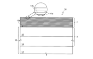
本発明は、特に、ワイドバンドギャップトランジスタにおける絶縁ゲート構造体の製造に関するものである。図1を参照すると、一般的に、ワイドバンドギャップトランジスタ1は、少なくとも1つの層が窒化ガリウム(GaN)又はシリコンカーバイド(SiC)等のワイドバンドギャップ半導体物質からなる半導体構造体2と、ソース電極3と、ドレイン電極4と、絶縁ゲート構造体8によって半導体構造体2から離隔されているゲート電極7と、を有している。より詳細には、半導体構造体2は、GaNHEMT装置の場合には、窒化アルミニウムガリウム(AlGaN)及びGaNヘテロ構造-AlGaN/GaNヘテロ構造を、又は、SiCMOSFETの場合には、高いドーピングレベル(例えば、1018子数/cm3はそれ以上)のSiC基板及び一層低いドーピングレベル(例えば、10151016子数/cm3のSiCエピタキシャル層を、包含する場合がある。 The present invention relates particularly to the fabrication of insulated gate structures in wide bandgap transistors. Referring to FIG. 1, a wide bandgap transistor 1 generally comprises a semiconductor structure 2, at least one layer of which is made of a wide bandgap semiconductor material such as gallium nitride (GaN) or silicon carbide (SiC), and a source electrode. 3 , a drain electrode 4 and a gate electrode 7 separated from the semiconductor structure 2 by an insulated gate structure 8 . More specifically, the semiconductor structure 2 comprises aluminum gallium nitride (AlGaN) and GaN heterostructures--AlGaN/GaN heterostructures in the case of GaN HEMT devices, or high doping levels (e.g. 10 18 atoms/cm 3 or more) and SiC epitaxial layers with even lower doping levels (eg, 10 15 10 16 atoms/cm 3 ) .
図2(a)-(c)により詳細に例示してある絶縁ゲート構造体8は、アルミニウム、ハフニウム、及び酸素の混合物を包含している。より詳細には、絶縁ゲート構造体8は、ゲート積層体8’(図2(a))を形成するためのナノメートルの厚さを有している複数のアルミニウム酸化物層8aと複数のハフニウム酸化物層8bの交互の相次いでのコンフォーマル付着とそれに続くアニーリング工程(図2(b)、(c))とによって得られる。アルミニウム酸化物層8a及びハフニウム酸化物層8bは、例えば、0.5nmと10nmとの間の厚さを有しており、アモルファスであり且つ原子層堆積法(ALD)によって得られる。層8a、8bの数は、絶縁ゲート構造体8の全体的な厚さが、例えば、30nmと60nmとの間の所望の値を有するように決定される。非制限的例においては、アルミニウム酸化物層8a及びハフニウム酸化物層8bの全ては等しい厚さを有している。 Insulated gate structure 8, illustrated in more detail in FIGS. 2(a)-(c), includes a mixture of aluminum, hafnium, and oxygen. More specifically, the insulated gate structure 8 comprises multiple aluminum oxide layers 8a and multiple hafnium Obtained by alternating successive conformal depositions of oxide layers 8b followed by an annealing step (FIGS. 2(b), (c)). The aluminum oxide layer 8a and the hafnium oxide layer 8b, for example, have a thickness between 0.5 nm and 10 nm, are amorphous and are obtained by atomic layer deposition (ALD). The number of layers 8a, 8b is determined such that the overall thickness of the insulated gate structure 8 has a desired value, for example between 30 nm and 60 nm. In a non-limiting example, the aluminum oxide layer 8a and the hafnium oxide layer 8b all have the same thickness.
アニーリング工程期間中に、層8a、8bの間の界面において、アルミニウム酸化物及びハフニウム酸化物が拡散し且つ混合する。従って、少なくとも、夫々の界面においては、アルミニウムと、ハフニウムと、酸素との混合物が存在している。アルミニウム酸化物層8a及びハフニウム酸化物層8bの初期厚さ、該アニーリング工程の期間及び温度に従って、最終的な絶縁ゲート構造体8において、初期の層状構造が部分的に残存されるか(図2(b))、又は、代替的に、失われる(図2(c))場合がある。該アニーリング工程は、ゲート積層体8’を500℃と950℃との間で、好適には600℃と800℃との間で、例えば800℃のアニーリング温度へ加熱させることによって実施することが可能である。そのアニーリング期間は30秒と600秒との間とすることが可能である。しかしながら、アニーリング温度とアニーリング期間とは、アルミニウム酸化物とハフニウム酸化物との拡散及び混合に起因する絶縁ゲート構造体8の結晶化を回避するように選択される。絶縁ゲート構造体8の誘電率及び結晶化温度は、アルミニウム酸化物の誘電率及び結晶化温度とハフニウム酸化物のそれとの中間である。従って、絶縁ゲート構造体8は満足のいく誘電率値を有しており、且つ、同時に、例えば、オーミックコンタクトの形成のためにパワー装置の製造工程期間中に発生する熱応力に構造的変形無しで耐えることが可能である。ゲート構造体は、高温度への露呈から保護することが必要ではないので、例えばフォトリソグラフィの数を減少させることによって不必要な工程を回避するように、その処理の流れを最適化させることが可能である。 During the annealing step aluminum oxide and hafnium oxide diffuse and mix at the interface between layers 8a, 8b. Therefore, at least at each interface, there is a mixture of aluminum, hafnium and oxygen. Depending on the initial thickness of the aluminum oxide layer 8a and the hafnium oxide layer 8b, the duration and temperature of the annealing step, whether the initial layered structure is partially preserved in the final insulated gate structure 8 (FIG. 2). (b)) or, alternatively, may be lost (FIG. 2(c)). The annealing step may be performed by heating the gate stack 8' between 500°C and 950°C, preferably between 600°C and 800°C, for example to an annealing temperature of 800°C. is. The annealing period can be between 30 and 600 seconds. However, the annealing temperature and duration are chosen to avoid crystallization of the insulated gate structure 8 due to diffusion and intermixing of aluminum oxide and hafnium oxide. The dielectric constant and crystallization temperature of the insulated gate structure 8 are intermediate those of aluminum oxide and hafnium oxide. Thus, the insulated gate structure 8 has a satisfactory dielectric constant value and at the same time is structurally free from thermal stresses occurring during the manufacturing process of the power device, e.g. for the formation of ohmic contacts. can be tolerated. Since the gate structure does not need to be protected from exposure to high temperatures, its process flow can be optimized to avoid unnecessary steps, for example by reducing the number of photolithography steps. It is possible.
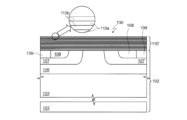
図3は、上述した如くに得られた絶縁ゲート構造体を具備するHEMT装置10を示している。HEMT装置10は、例えばシリコン又はシリコンカーバイド(SiC)又はアルミニウム酸化物(Al23からなる基板12と、基板12上に延在している真性窒化ガリウム(GaN)からなるチャンネル層14と、チャンネル層14上に延在している真性窒化アルミニウムガリウム(AlGaN)からなるか又はAlxa1-x、AlInGaN、Inxa1-x、Alxn1-xl等の窒化ガリウムの三元又は四元合金に基づく化合物からなるバリア層16と、チャンネル層14とは反対側のバリア層16の面16a上に延在している絶縁ゲート構造体17と、ソース電極20とドレイン電極22との間の絶縁ゲート構造体17の上を延在しているゲート電極18と、を包含している。
FIG. 3 shows a HEMT device 10 with an insulated gate structure obtained as described above. The HEMT device 10 comprises a
チャンネル層14及びバリア層16は、互いに界面においてヘテロ接合13aを具備しているヘテロ構造体13を形成している。従って、ヘテロ構造体13は、下側に存在する基板12との界面の一部であるチャンネル層14の底部側とバリア層16の上部側16aと間に延在している。
The
基板12、チャンネル層14、及びバリア層16は、以後、全体として、半導体構造体15として言及する。半導体構造体15内に画定される活性領域13aが、使用中に、HEMT装置10の導電性チャンネルを収容する。図3の実施例において、ゲート電極18は活性区域13aに対応するゾーンにおいて絶縁ゲート構造体17上を延在している。
図2(a)-(c)を参照して既に例示したようにして設けられる絶縁ゲート構造体17は、アルミニウムと、ハフニウムと、酸素との混合物を包含している。より詳細には、絶縁ゲート構造体17は、ナノメートル又はサブナノメートルの厚さを有している複数のアルミニウム酸化物層17a及び複数のハフニウム酸化物層17bの交互の相次いでのコンフォーマル付着(堆積)と、それに続くアニーリング工程とによって得られる。アルミニウム酸化物層17a及びハフニウム酸化物層17bはアモルファス、即ち非晶質、である。
The insulated
不図示の更なる実施例によれば、半導体ボディ15及びその中に収容されている活性領域13aとしてのウエルは、設計上の嗜好により、適宜にドープされているか又は真性型のGaN又はGaN合金の単一の層又は複数の層を有することが可能である。
According to a further embodiment not shown, the
図3の実施例においては、例えば金属である導電性物質からなるソース領域20及びドレイン領域22は、深くバリア層16内へ入り込むこと無しに、バリア層16の表面16aに到達するまで専ら絶縁ゲート層17を貫通して延在している。
In the embodiment of FIG. 3, the
不図示の実施例によれば、ソース領域20及びドレイン領域22が、バリア層16の厚さの一部にわたって延在しバリア層16内で終端するように延在している。
According to an embodiment not shown,
不図示の更なる実施例によれば、ソース領域20及びドレイン領域22は、完全にバリア層16を貫通して半導体ボディ15内深くに延在して、バリア層16とチャンネル層14との間の界面において終端している。
According to a further embodiment not shown, the
不図示の更なる実施例によれば、ソース領域20及びドレイン領域22は、更に、部分的にチャンネル領域14を介して延在し且つチャンネル層14内で終端している。
According to a further embodiment not shown,
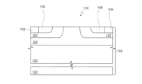
HEMT装置10の製造方法(プロセス)の1例について図4-9を参照して以下に説明する。 An example method (process) for manufacturing the HEMT device 10 is described below with reference to FIGS. 4-9.
最初に図4を参照すると、半導体ウエハ30は、例えばシリコン又はシリコンカーバイド(SiC)又はアルミニウム酸化物(Al23からなる基板12を有している。窒化ガリウム(GaN)のチャンネル層14及び窒化アルミニウムガリウム(AlGaN)のバリア層16を、チャンネル層14上に延在して、基板12上に形成する。バリア層16及びチャンネル層14は、前述したように、ヘテロ構造体13及びヘテロ接合13aを形成する。
Referring first to FIG. 4, a
次いで図2(a)を参照して説明した如く、ゲート積層体17’を形成する。特に、ゲート積層体17’は、ナノメートル厚さを有している複数のアルミニウム酸化物層17a及び複数のハフニウム酸化物層17b(HfO2を、所望の全体的な厚さに到達するまで、交互に相次いでのコンフォーマル付着(堆積)によって得られる。アルミニウム酸化物層17a及びハフニウム酸化物層17bはアモルファスであり且つ原子層堆積法(ALD)によって形成されるが、該方法は、構造のコンフォーマル特性及び極めて正確な厚さ制御を確保する。
A gate stack 17' is then formed as described with reference to FIG. 2(a). In particular, the gate stack 17' includes a plurality of
その後(図5)、例えばレジストの第1犠牲層25をゲート積層体17’上に形成し且つ第1フォトリソグラフィプロセスによって形状を画定させる。第1犠牲層25は、ソース電極20及びドレイン電極22を形成するための開口26を有している。第1犠牲層25は、開口26を介してゲート積層体17’を選択的にエッチするためのマスクとして使用される。
Thereafter (FIG. 5), a first
図6を参照すると、金属層又はマルチ層の付着と第1犠牲層25のリフトオフに続いて、夫々の開口26に対応する位置においてソース電極20及びドレイン電極22を形成する。
Referring to FIG. 6, following deposition of the metal layer or multi-layer and lift-off of the first
次いで、オーミックコンタクトを形成するために、例えば500℃と950℃との間で、好適には600℃と800℃との間の温度において、アニーリング工程を実施する。同時に、隣接するアルミニウム酸化物層17aとハフニウム酸化物層17bとが夫々の界面において互いに拡散し、且つ図7に示したように、ゲート積層体17’の残存する部分から絶縁ゲート構造体17が形成される。アルミニウム酸化物層17a及びハフニウム酸化物層17bの数及び厚さ、アニーリング温度、及びアニーリング期間は、絶縁ゲート構造体17が開始層17a、17bの痕跡を維持している(図2(b)の例におけるように)か、又は維持していない(図2(c)の例におけるように)し、且つ結晶化が回避されるように設計事項に従って選択される。
An annealing step is then performed, for example at a temperature between 500° C. and 950° C., preferably between 600° C. and 800° C., to form the ohmic contacts. At the same time, the adjacent
次いで、第2犠牲層27(図8)が絶縁ゲート構造体17上、ソース電極20上、及びドレイン電極22上に形成され、且つ第2フォトリソグラフィプロセスによって形状画定される。第2犠牲層27はゲート電極18を形成するための開口28を有している。
A second sacrificial layer 27 (FIG. 8) is then formed on the
金属層又はマルチ層の付着及び第2犠牲層27の(プラズマ又はウエット)エッチングによるリフトオフに続いて、開口28に対応する位置にゲート電極18を形成する。オプションとして、例えば400℃において、該金属層又はマルチ層の付着の後に更なるアニーリング工程を実施することが可能である。 Following deposition of the metal layer or multi-layer and lift-off of the second sacrificial layer 27 by (plasma or wet) etching, the gate electrode 18 is formed at locations corresponding to the openings 28 . Optionally, a further annealing step can be performed after deposition of the metal layer or multi-layers, for example at 400°C.
従来の且つ不図示の最終処理工程と半導体ウエハ30のダイシングの後に、図3のHEMT装置10が得られる。
After conventional and not shown final processing steps and dicing of the
アニーリング期間中のアルミニウム酸化物層17aとハフニウム酸化物層17bの拡散が、爾後の高温処理工程期間中に物質の結晶化を回避しながら、単一の真性のAl23びHfO2の誘電率値の間の典型的に中間の高い誘電率値を維持することを可能とする。特に、高温に対する耐性が、物質が劣化されること無しに、夫々のオーミックコンタクトを具備するソース電極及びドレイン電極を形成する前に、ゲート積層体17’を形成することを可能とする。この様に、絶縁ゲート構造体17を画定すると共に夫々のオーミックコンタクトを具備するソース電極及びドレイン電極を形成するために、単一のフォトリソグラフィプロセス及び単一のアニーリング工程を使用することが可能である。
Diffusion of the
異なる実施例の図9の場合、ここでは参照番号38で示したゲート領域は凹所型のものとすることが可能であり、且つ絶縁ゲート構造体40は平坦状ではない。この場合には、ALDによってコンフォーマルに付着された(図10)絶縁マルチ層40’を形成する前に、バリア層16を選択的にプラズマエッチしてトレンチ41を開口させる。
In a different embodiment, FIG. 9, the gate region, here indicated by reference numeral 38, may be of the recessed type and the insulated gate structure 40 is non-planar. In this case,
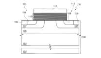
図11を参照すると、縦型MOSFET100が、シリコンカーバイド(SiC)の半導体構造体102を包含しており、その半導体構造体102の裏側102a上にドレイン電極100aを且つその半導体構造体102の正面側102b上にソース電極100bとゲート電極100cとを有している。半導体構造体102は、基板103(その一つの面は裏側100aを画定している)とエピタキシャル層105(その一つの面は半導体構造体102の正面側102bを画定している)とを包含しており、それらは両方とも例えばN型である第1導電型を有している。しかしながら、SiCのN型基板103は一層高い第1ドーピングレベル(例えば、1018子数/cm3上)を有しており、一方エピタキシャル層103は一層低い第2ドーピングレベル(例えば、10151016子数/cm3を有している。
Referring to FIG. 11, a vertical MOSFET 100 includes a silicon carbide (SiC)
ここではP型である第2導電型を有しているボディウエル107は、エピタキシャル層108の内部に形成されており、且つ特にN+である第1導電型のソース領域108及び特にP+である第2導電型で且つ夫々のソース領域108と隣接しているコンタクト領域109を収容している。エピタキシャル層105は電流スプレッド層(CSL)を画定しており、その中にはボディウエル107が埋設されている。
A body well 107 having a second conductivity type, here P-type, is formed within the
ボディウエル107は、通常、1μm未満で例えば0.6μmの距離だけ互いに離隔されている。ボディウエル107及びそれらの間に存在するエピタキシャル層105の部分は、寄生JFET領域を形成している。
The
絶縁ゲート構造体110が、ソース領域108の間のエピタキシャル層105上(又は、存在する場合には、エンハンスメント層6上)で半導体構造体102の正面側102a上を延在しており、且つその上にゲート電極100cが設けられている。図2(a)-(c)を参照して既に例示した如くに設けられた絶縁ゲート構造体110は、アルミニウムと、ハフニウムと、酸素との混合物を包含している。より詳細には、絶縁ゲート構造体110は、ナノメートル又はサブナノメートルの厚さを有している複数のアルミニウム酸化物層と複数のハフニウム酸化物層との交互の相次ぐコンフォーマル付着と、それに続くアニーリング工程とによって得られる。
An
図12乃至16を参照して、MOSFET100を製造するプロセス(方法)の1例について以下に説明する。 An example process for fabricating MOSFET 100 is described below with reference to FIGS.
最初に、図12を参照すると、半導体ウエハ130は基板103を有しており、その上にエピタキシャル層105が成長されて半導体構造体102を形成している。次いで、その後の異なるドーピング種のイオン注入によって、ボディウエル107、ソース領域108、及びコンタクト領域109を形成する。該イオン注入の後に、例えば1600℃を越える高温において活性化アニーリング工程を実施する。
First, referring to FIG. 12, a
次いで、図13を参照すると、図2(a)を参照して説明したように、ゲート積層体110’を形成する。特に、ゲート積層体110’は、全体的に所望の厚さに到達するまで、ナノメートル厚さを有している複数のアルミニウム酸化物層110aと複数のハフニウム酸化物層110bとの交互の相次ぐコンフォーマル付着(堆積)によって得られる。アルミニウム酸化物層110a及びハフニウム酸化物層110bは原子層堆積法(ALD)によって形成される。
13, gate stack 110' is formed as described with reference to FIG. 2(a). In particular, the gate stack 110' is composed of alternating successive layers of
図14に示したように、ゲート積層体110’上にレジストの第1犠牲層112を形成し且つ第1フォトリソグラフィプロセスによって形状画定させる。第1犠牲層112はソース電極100bの形成のための開口113を有しており且つゲート積層体110’を選択的にエッチするためのマスクとして使用される。
As shown in FIG. 14, a first
図15を参照すると、半導体構造体102の正面側102b上の金属層又はマルチ層の付着及び第1犠牲層112のリフトオフに続いて、夫々の開口113に対応する位置にソース電極100bを形成する。正面側102b上の付着と同時的に又はその後に、半導体構造体102の背面側102a上に金属層又はマルチ層を付着させてドレイン電極100aを形成する。ドレイン電極100aを付着させる前に、基板103を機械的に薄層化(研磨)させることが可能であり且つレーザーアニーリングに露呈させることが可能である。
Referring to FIG. 15, following deposition of a metal layer or multi-layer on the front side 102b of the
ドレイン電極100a及びソース電極100bが形成されると、例えば、シリサイドの形成のための800度のアニーリング温度において、アニーリング工程が実施される。この工程において、ゲート積層体110’がアニーリング温度へ加熱され、ゲート積層体110’のアルミニウム酸化物110a及びハフニウム酸化物110bが該界面において拡散し且つ混合する。従って、少なくとも該界面において、アルミニウムと、ハフニウムと、酸素との混合物が存在している。アルミニウム酸化物層8及びハフニウム酸化物層8bの初期厚さ、該アニーリング工程の期間及び温度、に従って、最終的な絶縁ゲート構造体110において、開始時の層状構造が部分的に維持される(図2(b)の例におけるように)か、又は、代替的に、喪失される(図2(c)の例におけるように)場合がある。
Once the drain electrode 100a and source electrode 100b are formed, an annealing step is performed, for example, at an annealing temperature of 800 degrees for silicide formation. In this step, the gate stack 110' is heated to the annealing temperature and the
アニーリングの後、図16を参照すると、ソース電極100bに使用される物質とは異なる物質の金属層又はマルチ層115が絶縁ゲート構造体110上及びソース電極100b上に付着され、次いで、該金属層又はマルチ層115の一部の上にレジストの第2犠牲層120が形成され且つ第2フォトリソグラフィプロセスによって形状画定される。第2犠牲層120はゲート電極100cを形成するための開口121を有している。第2犠牲層120は、例えば、プラズマエッチングによって開口121を介して金属層又はマルチ層115を選択的にエッチするためのマスクとして使用される。従って、ゲート電極100cが得られる。
After annealing, referring to FIG. 16, a metal layer or multi-layer 115 of a material different from the material used for the source electrode 100b is deposited over the
従来の且つ不図示の最終的な処理工程及び半導体ウエハ30のダイシングの後に、図11のMOSFET100が得られる。
After conventional and not shown final processing steps and dicing of
上述した絶縁ゲート構造体117及びその製造方法(プロセス)は、例えば、二重の利点で、シリコン酸化物の代わりにSiCMOSFETにおけるゲート絶縁体として高誘電率誘電体を使用することを可能とする。実際に、一方においては、高い誘電率は、エピタキシャル層105内に最も高い電界値を局所化させることを可能とする。従って、同じエピタキシャル層105の厚さ及びオン状態抵抗RONの両方を最適化させることが可能である。他方において、高温(1100-1200℃)においての窒化酸化物酸化後アニーリング工程が除去されているので、処理の流れが簡単化されている。
The insulated gate structure 117 and its fabrication process described above, for example, allow the use of high-k dielectrics as gate insulators in SiCMOSFETs in place of silicon oxide, with dual advantages. In fact, on the one hand, a high dielectric constant makes it possible to localize the highest electric field values within the
以上、本発明の具体的実施の態様について詳細に説明したが、本発明はこれらの具体的実施の態様に制限されるべきものではなく、本発明の技術的範囲を逸脱すること無しに種々の変形及び修正を行うことが可能であることは勿論である。 Although specific embodiments of the present invention have been described in detail above, the present invention should not be limited to these specific embodiments, and various modifications may be made without departing from the technical scope of the present invention. Variations and modifications are of course possible.
Claims (15)
窒化ガリウム(GaN)又はシリコンカーバイド(SiC)の少なくとも一つのワイドバンドギャップ半導体層(14,16;103,105)を包含している半導体構造体(2;15;102)、
絶縁ゲート構造体(8;17;110)、
該絶縁ゲート構造体(8;17;110)によって該半導体構造体(2;15;102)から離隔されているゲート電極(7;18;100c)、
を有しており、該絶縁ゲート構造体(8;17;110)がアルミニウムと、ハフニウムと、酸素との混合物を包含しているワイドバンドギャップトランジスタ。 In a wide bandgap transistor,
a semiconductor structure (2; 15; 102) comprising at least one wide bandgap semiconductor layer (14, 16; 103, 105) of gallium nitride (GaN) or silicon carbide (SiC);
an insulated gate structure (8;17;110),
a gate electrode (7;18;100c) separated from said semiconductor structure (2;15;102) by said insulating gate structure (8;17;110);
and wherein said insulated gate structure (8; 17; 110) comprises a mixture of aluminum, hafnium and oxygen.
或る導電型と第1ドーピングレベルとを有しているシリコンカーバイド(SiC)の基板(103)と、
前記導電型と該第1ドーピングレベルよりも一層低い第2ドーピングレベルを有しているシリコンカーバイド(SiC)のエピタキシャル層(105)と、
を有している請求項1に記載のトランジスタ。 The semiconductor structure (102) comprises:
a substrate (103) of silicon carbide (SiC) having a conductivity type and a first doping level;
an epitaxial layer (105) of silicon carbide (SiC) having said conductivity type and a second doping level lower than said first doping level;
2. The transistor of claim 1, comprising:
窒化ガリウム(GaN)又はシリコンカーバイド(SiC)の少なくとも一つのワイドバンドギャップ半導体層(14,16;103,105)を包含している半導体構造体(2;15;102)を形成し、
該半導体構造体(2;15;102)の上に絶縁ゲート構造体(8;17;110)を形成し、
該絶縁ゲート構造体(8;17;110)の上にゲート電極(7;18;100c)を形成する、
ことを包含しており、該絶縁ゲート構造体(8;17;110)がアルミニウムと、ハフニウムと、酸素との混合物を包含している方法。 In a method of manufacturing a wide bandgap transistor,
forming a semiconductor structure (2; 15; 102) including at least one wide bandgap semiconductor layer (14, 16; 103, 105) of gallium nitride (GaN) or silicon carbide (SiC);
forming an insulated gate structure (8;17;110) over the semiconductor structure (2;15;102);
forming a gate electrode (7;18;100c) over the insulated gate structure (8;17;110);
and wherein said insulated gate structure (8;17;110) comprises a mixture of aluminum, hafnium and oxygen.
窒化ガリウム(GaN)のチャンネル層(14)と窒化アルミニウムガリウム(AlGaN)のバリア層(16)とを包含しておりヘテロ接合(13a)が該チャンネル層(14)と該バリア層(16)との間の界面に形成されているヘテロ構造体(13)を形成することを包含している請求項7に記載の方法。 forming the semiconductor structure (2;15;102);
a gallium nitride (GaN) channel layer (14) and an aluminum gallium nitride (AlGaN) barrier layer (16), wherein a heterojunction (13a) is formed between the channel layer (14) and the barrier layer (16); 8. The method of claim 7 including forming a heterostructure (13) formed at an interface between.
或る導電型及び第1ドーピングレベルを有しているシリコンカーバイド(SiC)の基板(103)を形成すること、及び
前記導電型及び該第1ドーピングレベルよりも一層低い第2ドーピングレベルを有しているシリコンカーバイド(SiC)のエピタキシャル層(105)を形成すること、
を包含している請求項7に記載の方法。 Forming the semiconductor structure (102) comprises:
forming a substrate (103) of silicon carbide (SiC) having a conductivity type and a first doping level; and having a second doping level lower than said conductivity type and said first doping level. forming an epitaxial layer (105) of silicon carbide (SiC) comprising
8. The method of claim 7, comprising:
複数のアルミニウム酸化物層(8a;17a;110a)及び複数のハフニウム酸化物層(8b;17b;110b)を交互に相次いで付着させてゲート積層体(8’;17’;110’)を形成すること、及び
隣接するアルミニウム酸化物層(8a:17a:110a)とハフニウム酸化物層(8b;17b;110b)との間の界面において該アルミニウム酸化物層(8a;17a;110a)のアルミニウム酸化物と該ハフニウム酸化物層(8b;17b;110b)のハフニウム酸化物とが拡散して混合するようにアニーリングを実施すること、
を包含している請求項7乃至9の内のいずれか1項に記載の方法。 forming the insulated gate structure (8;17;110);
A plurality of aluminum oxide layers (8a; 17a; 110a) and a plurality of hafnium oxide layers (8b; 17b; 110b) are deposited in alternating succession to form a gate stack (8';17';110'). and aluminum oxidation of the aluminum oxide layer (8a; 17a; 110a) at the interface between the adjacent aluminum oxide layer (8a:17a:110a) and the hafnium oxide layer (8b; 17b; 110b) performing annealing such that the material and the hafnium oxide of the hafnium oxide layer (8b; 17b; 110b) diffuse and mix;
10. A method according to any one of claims 7-9, comprising:
或るアニーリング期間の間或るアニーリング温度へ該ゲート積層体(8’;17’;110’)へ加熱することを包含しており、該アニーリング温度及び該アニーリング期間は該絶縁ゲート構造体(8;17;110)が結晶化することを防止するように選択されている請求項10に記載の方法。 Carrying out annealing
heating the gate stack (8';17';110') to an annealing temperature for an annealing period, the annealing temperature and the annealing period being the same as the insulating gate structure (8 17; 110) are selected to prevent crystallization.
Applications Claiming Priority (2)
| Application Number | Priority Date | Filing Date | Title |
|---|---|---|---|
| IT102022000001478A IT202200001478A1 (en) | 2022-01-28 | 2022-01-28 | WIDE BAND TRANSISTOR WITH NANOLAMINATE GATE INSULATING STRUCTURE AND METHOD FOR MANUFACTURING A WIDE BAND TRANSISTOR |
| IT102022000001478 | 2022-01-28 |
Publications (1)
| Publication Number | Publication Date |
|---|---|
| JP2023110900A true JP2023110900A (en) | 2023-08-09 |
Family
ID=80933659
Family Applications (1)
| Application Number | Title | Priority Date | Filing Date |
|---|---|---|---|
| JP2023010393A Pending JP2023110900A (en) | 2022-01-28 | 2023-01-26 | Wide band gap transistor with nanolaminated insulating gate structure and method for manufacturing wide band gap transistor |
Country Status (4)
| Country | Link |
|---|---|
| US (1) | US20230246086A1 (en) |
| EP (1) | EP4220734A1 (en) |
| JP (1) | JP2023110900A (en) |
| IT (1) | IT202200001478A1 (en) |
-
2022
- 2022-01-28 IT IT102022000001478A patent/IT202200001478A1/en unknown
-
2023
- 2023-01-18 US US18/156,120 patent/US20230246086A1/en active Pending
- 2023-01-19 EP EP23152421.6A patent/EP4220734A1/en active Pending
- 2023-01-26 JP JP2023010393A patent/JP2023110900A/en active Pending
Also Published As
| Publication number | Publication date |
|---|---|
| IT202200001478A1 (en) | 2023-07-28 |
| EP4220734A1 (en) | 2023-08-02 |
| US20230246086A1 (en) | 2023-08-03 |
Similar Documents
| Publication | Publication Date | Title |
|---|---|---|
| US8658503B2 (en) | Semiconductor device and method of fabricating the same | |
| TWI445093B (en) | Iii-nitride devices with recessed gates | |
| US9520489B2 (en) | Semiconductor device | |
| JP5584823B2 (en) | Silicon carbide semiconductor device | |
| KR20150070001A (en) | Semiconductor device | |
| JP2013012735A (en) | Cmos compatible method for manufacturing hemt device and hemt device thereof | |
| JP2012044003A (en) | Semiconductor device and manufacturing method of the same | |
| JP2014146666A (en) | Semiconductor device | |
| CN111048420B (en) | Method for manufacturing lateral double-diffused transistor | |
| WO2013027471A1 (en) | Semiconductor device | |
| JP2019186458A (en) | Switching element and manufacturing method therefor | |
| JP6560117B2 (en) | Manufacturing method of semiconductor device | |
| JP4948784B2 (en) | Semiconductor device and manufacturing method thereof | |
| JP2014241350A (en) | Field effect transistor and manufacturing method thereof | |
| JP2010027833A (en) | Silicon carbide semiconductor device and its manufacturing method | |
| US8558242B2 (en) | Vertical GaN-based metal insulator semiconductor FET | |
| JP6648852B1 (en) | Silicon carbide semiconductor device and method of manufacturing silicon carbide semiconductor device | |
| JP7165328B2 (en) | Semiconductor device and method for manufacturing semiconductor device | |
| TWI546958B (en) | Gold and oxygen semi - high electron mobility transistor | |
| JP2023110900A (en) | Wide band gap transistor with nanolaminated insulating gate structure and method for manufacturing wide band gap transistor | |
| CN110676166B (en) | FinFET enhanced device with P-GaN cap layer and manufacturing method thereof | |
| KR102067596B1 (en) | Nitride semiconductor and method thereof | |
| JP2021009989A (en) | Nitride semiconductor device | |
| CN116525669A (en) | Wide bandgap transistor with nanolaminated insulated gate structure and fabrication process | |
| JP2021111666A (en) | Compound semiconductor device and method for manufacturing compound semiconductor device |
Legal Events
| Date | Code | Title | Description |
|---|---|---|---|
| RD03 | Notification of appointment of power of attorney |
Free format text: JAPANESE INTERMEDIATE CODE: A7423 Effective date: 20240308 |