JP2022176166A - Semiconductor device, display device, and electronic device - Google Patents
Semiconductor device, display device, and electronic device Download PDFInfo
- Publication number
- JP2022176166A JP2022176166A JP2022078958A JP2022078958A JP2022176166A JP 2022176166 A JP2022176166 A JP 2022176166A JP 2022078958 A JP2022078958 A JP 2022078958A JP 2022078958 A JP2022078958 A JP 2022078958A JP 2022176166 A JP2022176166 A JP 2022176166A
- Authority
- JP
- Japan
- Prior art keywords
- transistor
- circuit
- terminal
- gate
- wiring
- Prior art date
- Legal status (The legal status is an assumption and is not a legal conclusion. Google has not performed a legal analysis and makes no representation as to the accuracy of the status listed.)
- Pending
Links
- 239000004065 semiconductor Substances 0.000 title claims abstract description 169
- 239000003990 capacitor Substances 0.000 claims abstract description 142
- 239000010410 layer Substances 0.000 description 556
- 239000012212 insulator Substances 0.000 description 342
- 239000004020 conductor Substances 0.000 description 308
- 230000006870 function Effects 0.000 description 166
- 239000010408 film Substances 0.000 description 164
- 239000000758 substrate Substances 0.000 description 120
- 239000000463 material Substances 0.000 description 114
- 238000000034 method Methods 0.000 description 99
- 238000003384 imaging method Methods 0.000 description 70
- 238000010586 diagram Methods 0.000 description 50
- 239000007789 gas Substances 0.000 description 42
- 102100040862 Dual specificity protein kinase CLK1 Human genes 0.000 description 41
- 101000749294 Homo sapiens Dual specificity protein kinase CLK1 Proteins 0.000 description 41
- 238000006243 chemical reaction Methods 0.000 description 38
- 238000002347 injection Methods 0.000 description 33
- 239000007924 injection Substances 0.000 description 33
- 229910044991 metal oxide Inorganic materials 0.000 description 31
- 150000004706 metal oxides Chemical class 0.000 description 31
- 239000001257 hydrogen Substances 0.000 description 30
- 229910052739 hydrogen Inorganic materials 0.000 description 30
- 101150063259 VDE1 gene Proteins 0.000 description 29
- 230000002829 reductive effect Effects 0.000 description 29
- XUIMIQQOPSSXEZ-UHFFFAOYSA-N Silicon Chemical compound [Si] XUIMIQQOPSSXEZ-UHFFFAOYSA-N 0.000 description 27
- 229910052751 metal Inorganic materials 0.000 description 27
- 239000002184 metal Substances 0.000 description 27
- 229910052710 silicon Inorganic materials 0.000 description 27
- 239000010703 silicon Substances 0.000 description 27
- 102100040844 Dual specificity protein kinase CLK2 Human genes 0.000 description 26
- 101000749291 Homo sapiens Dual specificity protein kinase CLK2 Proteins 0.000 description 26
- 239000012535 impurity Substances 0.000 description 26
- 239000000126 substance Substances 0.000 description 26
- UFHFLCQGNIYNRP-UHFFFAOYSA-N Hydrogen Chemical compound [H][H] UFHFLCQGNIYNRP-UHFFFAOYSA-N 0.000 description 25
- 230000008859 change Effects 0.000 description 25
- 238000004519 manufacturing process Methods 0.000 description 25
- 239000011347 resin Substances 0.000 description 25
- 229920005989 resin Polymers 0.000 description 25
- IJGRMHOSHXDMSA-UHFFFAOYSA-N Atomic nitrogen Chemical compound N#N IJGRMHOSHXDMSA-UHFFFAOYSA-N 0.000 description 22
- 230000005525 hole transport Effects 0.000 description 21
- 230000004888 barrier function Effects 0.000 description 19
- 239000003086 colorant Substances 0.000 description 19
- XLYOFNOQVPJJNP-UHFFFAOYSA-N water Substances O XLYOFNOQVPJJNP-UHFFFAOYSA-N 0.000 description 19
- 229910001868 water Inorganic materials 0.000 description 19
- 229910052581 Si3N4 Inorganic materials 0.000 description 18
- 239000012790 adhesive layer Substances 0.000 description 18
- 230000015572 biosynthetic process Effects 0.000 description 18
- HQVNEWCFYHHQES-UHFFFAOYSA-N silicon nitride Chemical compound N12[Si]34N5[Si]62N3[Si]51N64 HQVNEWCFYHHQES-UHFFFAOYSA-N 0.000 description 18
- 229910052782 aluminium Inorganic materials 0.000 description 17
- 238000012937 correction Methods 0.000 description 17
- 210000001508 eye Anatomy 0.000 description 17
- 239000010437 gem Substances 0.000 description 17
- 229910001751 gemstone Inorganic materials 0.000 description 17
- 229910052760 oxygen Inorganic materials 0.000 description 17
- 239000011701 zinc Substances 0.000 description 17
- XAGFODPZIPBFFR-UHFFFAOYSA-N aluminium Chemical group [Al] XAGFODPZIPBFFR-UHFFFAOYSA-N 0.000 description 16
- 230000000694 effects Effects 0.000 description 16
- 239000011159 matrix material Substances 0.000 description 16
- 238000003860 storage Methods 0.000 description 16
- QVGXLLKOCUKJST-UHFFFAOYSA-N atomic oxygen Chemical compound [O] QVGXLLKOCUKJST-UHFFFAOYSA-N 0.000 description 15
- -1 element M Chemical compound 0.000 description 15
- 239000001301 oxygen Substances 0.000 description 15
- 238000012545 processing Methods 0.000 description 15
- 238000000231 atomic layer deposition Methods 0.000 description 13
- 150000004767 nitrides Chemical class 0.000 description 13
- WFKWXMTUELFFGS-UHFFFAOYSA-N tungsten Chemical compound [W] WFKWXMTUELFFGS-UHFFFAOYSA-N 0.000 description 13
- 229910052721 tungsten Inorganic materials 0.000 description 13
- 239000010937 tungsten Substances 0.000 description 13
- 150000001875 compounds Chemical class 0.000 description 12
- 238000009792 diffusion process Methods 0.000 description 12
- 230000001276 controlling effect Effects 0.000 description 11
- 230000033001 locomotion Effects 0.000 description 11
- 229910052757 nitrogen Inorganic materials 0.000 description 11
- 230000003071 parasitic effect Effects 0.000 description 11
- XLOMVQKBTHCTTD-UHFFFAOYSA-N Zinc monoxide Chemical compound [Zn]=O XLOMVQKBTHCTTD-UHFFFAOYSA-N 0.000 description 10
- 229910010272 inorganic material Inorganic materials 0.000 description 10
- TWNQGVIAIRXVLR-UHFFFAOYSA-N oxo(oxoalumanyloxy)alumane Chemical compound O=[Al]O[Al]=O TWNQGVIAIRXVLR-UHFFFAOYSA-N 0.000 description 10
- 239000002243 precursor Substances 0.000 description 10
- 238000007789 sealing Methods 0.000 description 10
- VYPSYNLAJGMNEJ-UHFFFAOYSA-N silicon dioxide Inorganic materials O=[Si]=O VYPSYNLAJGMNEJ-UHFFFAOYSA-N 0.000 description 10
- 238000005229 chemical vapour deposition Methods 0.000 description 9
- 229910052738 indium Inorganic materials 0.000 description 9
- APFVFJFRJDLVQX-UHFFFAOYSA-N indium atom Chemical compound [In] APFVFJFRJDLVQX-UHFFFAOYSA-N 0.000 description 9
- 239000011241 protective layer Substances 0.000 description 9
- 239000002096 quantum dot Substances 0.000 description 9
- 229910052814 silicon oxide Inorganic materials 0.000 description 9
- XMWRBQBLMFGWIX-UHFFFAOYSA-N C60 fullerene Chemical class C12=C3C(C4=C56)=C7C8=C5C5=C9C%10=C6C6=C4C1=C1C4=C6C6=C%10C%10=C9C9=C%11C5=C8C5=C8C7=C3C3=C7C2=C1C1=C2C4=C6C4=C%10C6=C9C9=C%11C5=C5C8=C3C3=C7C1=C1C2=C4C6=C2C9=C5C3=C12 XMWRBQBLMFGWIX-UHFFFAOYSA-N 0.000 description 8
- HCHKCACWOHOZIP-UHFFFAOYSA-N Zinc Chemical compound [Zn] HCHKCACWOHOZIP-UHFFFAOYSA-N 0.000 description 8
- 239000011229 interlayer Substances 0.000 description 8
- 229920000642 polymer Polymers 0.000 description 8
- 229910052725 zinc Inorganic materials 0.000 description 8
- RYGMFSIKBFXOCR-UHFFFAOYSA-N Copper Chemical group [Cu] RYGMFSIKBFXOCR-UHFFFAOYSA-N 0.000 description 7
- 229910052735 hafnium Inorganic materials 0.000 description 7
- 239000011261 inert gas Substances 0.000 description 7
- 230000007246 mechanism Effects 0.000 description 7
- 239000007800 oxidant agent Substances 0.000 description 7
- GYHNNYVSQQEPJS-UHFFFAOYSA-N Gallium Chemical group [Ga] GYHNNYVSQQEPJS-UHFFFAOYSA-N 0.000 description 6
- MWUXSHHQAYIFBG-UHFFFAOYSA-N Nitric oxide Chemical compound O=[N] MWUXSHHQAYIFBG-UHFFFAOYSA-N 0.000 description 6
- 238000013473 artificial intelligence Methods 0.000 description 6
- 238000004364 calculation method Methods 0.000 description 6
- 239000000969 carrier Substances 0.000 description 6
- 239000010949 copper Chemical group 0.000 description 6
- PMHQVHHXPFUNSP-UHFFFAOYSA-M copper(1+);methylsulfanylmethane;bromide Chemical compound Br[Cu].CSC PMHQVHHXPFUNSP-UHFFFAOYSA-M 0.000 description 6
- 229910052733 gallium Inorganic materials 0.000 description 6
- 238000002955 isolation Methods 0.000 description 6
- 239000007788 liquid Substances 0.000 description 6
- 230000008569 process Effects 0.000 description 6
- 238000007740 vapor deposition Methods 0.000 description 6
- 230000005540 biological transmission Effects 0.000 description 5
- 230000000295 complement effect Effects 0.000 description 5
- 229910052802 copper Inorganic materials 0.000 description 5
- 238000000151 deposition Methods 0.000 description 5
- 229910003472 fullerene Inorganic materials 0.000 description 5
- 229910052732 germanium Inorganic materials 0.000 description 5
- GNPVGFCGXDBREM-UHFFFAOYSA-N germanium atom Chemical compound [Ge] GNPVGFCGXDBREM-UHFFFAOYSA-N 0.000 description 5
- 239000011521 glass Substances 0.000 description 5
- VBJZVLUMGGDVMO-UHFFFAOYSA-N hafnium atom Chemical compound [Hf] VBJZVLUMGGDVMO-UHFFFAOYSA-N 0.000 description 5
- 229910000449 hafnium oxide Inorganic materials 0.000 description 5
- WIHZLLGSGQNAGK-UHFFFAOYSA-N hafnium(4+);oxygen(2-) Chemical compound [O-2].[O-2].[Hf+4] WIHZLLGSGQNAGK-UHFFFAOYSA-N 0.000 description 5
- 210000003128 head Anatomy 0.000 description 5
- 150000002431 hydrogen Chemical class 0.000 description 5
- 150000002484 inorganic compounds Chemical class 0.000 description 5
- 239000011147 inorganic material Substances 0.000 description 5
- 239000002346 layers by function Substances 0.000 description 5
- 239000000203 mixture Substances 0.000 description 5
- 238000000206 photolithography Methods 0.000 description 5
- 238000005498 polishing Methods 0.000 description 5
- 238000007639 printing Methods 0.000 description 5
- 239000002994 raw material Substances 0.000 description 5
- 238000002230 thermal chemical vapour deposition Methods 0.000 description 5
- 239000010409 thin film Substances 0.000 description 5
- 239000010936 titanium Substances 0.000 description 5
- 229910052719 titanium Inorganic materials 0.000 description 5
- 239000011787 zinc oxide Substances 0.000 description 5
- XKRFYHLGVUSROY-UHFFFAOYSA-N Argon Chemical compound [Ar] XKRFYHLGVUSROY-UHFFFAOYSA-N 0.000 description 4
- ZOXJGFHDIHLPTG-UHFFFAOYSA-N Boron Chemical compound [B] ZOXJGFHDIHLPTG-UHFFFAOYSA-N 0.000 description 4
- XEEYBQQBJWHFJM-UHFFFAOYSA-N Iron Chemical compound [Fe] XEEYBQQBJWHFJM-UHFFFAOYSA-N 0.000 description 4
- HBBGRARXTFLTSG-UHFFFAOYSA-N Lithium ion Chemical compound [Li+] HBBGRARXTFLTSG-UHFFFAOYSA-N 0.000 description 4
- PXHVJJICTQNCMI-UHFFFAOYSA-N Nickel Chemical compound [Ni] PXHVJJICTQNCMI-UHFFFAOYSA-N 0.000 description 4
- 229910000577 Silicon-germanium Inorganic materials 0.000 description 4
- BQCADISMDOOEFD-UHFFFAOYSA-N Silver Chemical compound [Ag] BQCADISMDOOEFD-UHFFFAOYSA-N 0.000 description 4
- ATJFFYVFTNAWJD-UHFFFAOYSA-N Tin Chemical group [Sn] ATJFFYVFTNAWJD-UHFFFAOYSA-N 0.000 description 4
- 239000000956 alloy Substances 0.000 description 4
- 229910052796 boron Inorganic materials 0.000 description 4
- 239000000872 buffer Substances 0.000 description 4
- 238000004891 communication Methods 0.000 description 4
- 230000000875 corresponding effect Effects 0.000 description 4
- 238000013461 design Methods 0.000 description 4
- 238000005530 etching Methods 0.000 description 4
- 238000010438 heat treatment Methods 0.000 description 4
- AMGQUBHHOARCQH-UHFFFAOYSA-N indium;oxotin Chemical compound [In].[Sn]=O AMGQUBHHOARCQH-UHFFFAOYSA-N 0.000 description 4
- 239000011810 insulating material Substances 0.000 description 4
- 239000004973 liquid crystal related substance Substances 0.000 description 4
- 229910001416 lithium ion Inorganic materials 0.000 description 4
- 238000004768 lowest unoccupied molecular orbital Methods 0.000 description 4
- 230000004048 modification Effects 0.000 description 4
- 238000012986 modification Methods 0.000 description 4
- 150000002894 organic compounds Chemical class 0.000 description 4
- 239000011368 organic material Substances 0.000 description 4
- 239000012466 permeate Substances 0.000 description 4
- 238000004549 pulsed laser deposition Methods 0.000 description 4
- 229910052709 silver Inorganic materials 0.000 description 4
- 239000004332 silver Substances 0.000 description 4
- 238000004544 sputter deposition Methods 0.000 description 4
- MZLGASXMSKOWSE-UHFFFAOYSA-N tantalum nitride Chemical compound [Ta]#N MZLGASXMSKOWSE-UHFFFAOYSA-N 0.000 description 4
- 229910052718 tin Inorganic materials 0.000 description 4
- 238000012546 transfer Methods 0.000 description 4
- 239000004925 Acrylic resin Substances 0.000 description 3
- 229920000178 Acrylic resin Polymers 0.000 description 3
- 101100191136 Arabidopsis thaliana PCMP-A2 gene Proteins 0.000 description 3
- JBRZTFJDHDCESZ-UHFFFAOYSA-N AsGa Chemical compound [As]#[Ga] JBRZTFJDHDCESZ-UHFFFAOYSA-N 0.000 description 3
- UHOVQNZJYSORNB-UHFFFAOYSA-N Benzene Chemical compound C1=CC=CC=C1 UHOVQNZJYSORNB-UHFFFAOYSA-N 0.000 description 3
- WHXSMMKQMYFTQS-UHFFFAOYSA-N Lithium Chemical compound [Li] WHXSMMKQMYFTQS-UHFFFAOYSA-N 0.000 description 3
- FYYHWMGAXLPEAU-UHFFFAOYSA-N Magnesium Chemical compound [Mg] FYYHWMGAXLPEAU-UHFFFAOYSA-N 0.000 description 3
- ZOKXTWBITQBERF-UHFFFAOYSA-N Molybdenum Chemical compound [Mo] ZOKXTWBITQBERF-UHFFFAOYSA-N 0.000 description 3
- KDLHZDBZIXYQEI-UHFFFAOYSA-N Palladium Chemical compound [Pd] KDLHZDBZIXYQEI-UHFFFAOYSA-N 0.000 description 3
- 101100422768 Saccharomyces cerevisiae (strain ATCC 204508 / S288c) SUL2 gene Proteins 0.000 description 3
- 101100048260 Saccharomyces cerevisiae (strain ATCC 204508 / S288c) UBX2 gene Proteins 0.000 description 3
- RTAQQCXQSZGOHL-UHFFFAOYSA-N Titanium Chemical compound [Ti] RTAQQCXQSZGOHL-UHFFFAOYSA-N 0.000 description 3
- 230000009471 action Effects 0.000 description 3
- 230000003321 amplification Effects 0.000 description 3
- 210000005252 bulbus oculi Anatomy 0.000 description 3
- 238000000576 coating method Methods 0.000 description 3
- 239000000470 constituent Substances 0.000 description 3
- 230000008878 coupling Effects 0.000 description 3
- 238000010168 coupling process Methods 0.000 description 3
- 238000005859 coupling reaction Methods 0.000 description 3
- 238000003795 desorption Methods 0.000 description 3
- 238000001514 detection method Methods 0.000 description 3
- AJNVQOSZGJRYEI-UHFFFAOYSA-N digallium;oxygen(2-) Chemical compound [O-2].[O-2].[O-2].[Ga+3].[Ga+3] AJNVQOSZGJRYEI-UHFFFAOYSA-N 0.000 description 3
- 239000003822 epoxy resin Substances 0.000 description 3
- 238000007667 floating Methods 0.000 description 3
- 229910001195 gallium oxide Inorganic materials 0.000 description 3
- PCHJSUWPFVWCPO-UHFFFAOYSA-N gold Chemical compound [Au] PCHJSUWPFVWCPO-UHFFFAOYSA-N 0.000 description 3
- 229910052737 gold Inorganic materials 0.000 description 3
- 239000010931 gold Substances 0.000 description 3
- 238000004770 highest occupied molecular orbital Methods 0.000 description 3
- 125000004435 hydrogen atom Chemical group [H]* 0.000 description 3
- 230000006872 improvement Effects 0.000 description 3
- 229910052744 lithium Inorganic materials 0.000 description 3
- 239000011777 magnesium Substances 0.000 description 3
- 239000007769 metal material Substances 0.000 description 3
- 229910052750 molybdenum Inorganic materials 0.000 description 3
- 239000011733 molybdenum Substances 0.000 description 3
- 238000003199 nucleic acid amplification method Methods 0.000 description 3
- 230000001151 other effect Effects 0.000 description 3
- 230000001590 oxidative effect Effects 0.000 description 3
- 230000002093 peripheral effect Effects 0.000 description 3
- IEQIEDJGQAUEQZ-UHFFFAOYSA-N phthalocyanine Chemical compound N1C(N=C2C3=CC=CC=C3C(N=C3C4=CC=CC=C4C(=N4)N3)=N2)=C(C=CC=C2)C2=C1N=C1C2=CC=CC=C2C4=N1 IEQIEDJGQAUEQZ-UHFFFAOYSA-N 0.000 description 3
- 238000005240 physical vapour deposition Methods 0.000 description 3
- 229920000647 polyepoxide Polymers 0.000 description 3
- 150000003254 radicals Chemical class 0.000 description 3
- 239000002356 single layer Substances 0.000 description 3
- 239000007787 solid Substances 0.000 description 3
- PFNQVRZLDWYSCW-UHFFFAOYSA-N (fluoren-9-ylideneamino) n-naphthalen-1-ylcarbamate Chemical compound C12=CC=CC=C2C2=CC=CC=C2C1=NOC(=O)NC1=CC=CC2=CC=CC=C12 PFNQVRZLDWYSCW-UHFFFAOYSA-N 0.000 description 2
- WUPHOULIZUERAE-UHFFFAOYSA-N 3-(oxolan-2-yl)propanoic acid Chemical compound OC(=O)CCC1CCCO1 WUPHOULIZUERAE-UHFFFAOYSA-N 0.000 description 2
- OKTJSMMVPCPJKN-UHFFFAOYSA-N Carbon Chemical compound [C] OKTJSMMVPCPJKN-UHFFFAOYSA-N 0.000 description 2
- 229910052684 Cerium Inorganic materials 0.000 description 2
- JMASRVWKEDWRBT-UHFFFAOYSA-N Gallium nitride Chemical compound [Ga]#N JMASRVWKEDWRBT-UHFFFAOYSA-N 0.000 description 2
- 229910052779 Neodymium Inorganic materials 0.000 description 2
- GQPLMRYTRLFLPF-UHFFFAOYSA-N Nitrous Oxide Chemical compound [O-][N+]#N GQPLMRYTRLFLPF-UHFFFAOYSA-N 0.000 description 2
- OAICVXFJPJFONN-UHFFFAOYSA-N Phosphorus Chemical compound [P] OAICVXFJPJFONN-UHFFFAOYSA-N 0.000 description 2
- 229920001609 Poly(3,4-ethylenedioxythiophene) Polymers 0.000 description 2
- 239000004372 Polyvinyl alcohol Substances 0.000 description 2
- 239000007983 Tris buffer Substances 0.000 description 2
- QCWXUUIWCKQGHC-UHFFFAOYSA-N Zirconium Chemical compound [Zr] QCWXUUIWCKQGHC-UHFFFAOYSA-N 0.000 description 2
- LEVVHYCKPQWKOP-UHFFFAOYSA-N [Si].[Ge] Chemical compound [Si].[Ge] LEVVHYCKPQWKOP-UHFFFAOYSA-N 0.000 description 2
- 238000010521 absorption reaction Methods 0.000 description 2
- 230000001133 acceleration Effects 0.000 description 2
- 239000002253 acid Substances 0.000 description 2
- 239000008186 active pharmaceutical agent Substances 0.000 description 2
- 229910052784 alkaline earth metal Inorganic materials 0.000 description 2
- 229910045601 alloy Inorganic materials 0.000 description 2
- MDPILPRLPQYEEN-UHFFFAOYSA-N aluminium arsenide Chemical compound [As]#[Al] MDPILPRLPQYEEN-UHFFFAOYSA-N 0.000 description 2
- 229910021417 amorphous silicon Inorganic materials 0.000 description 2
- 150000001454 anthracenes Chemical class 0.000 description 2
- 229910052786 argon Inorganic materials 0.000 description 2
- 125000004429 atom Chemical group 0.000 description 2
- WZJYKHNJTSNBHV-UHFFFAOYSA-N benzo[h]quinoline Chemical class C1=CN=C2C3=CC=CC=C3C=CC2=C1 WZJYKHNJTSNBHV-UHFFFAOYSA-N 0.000 description 2
- 229910052790 beryllium Inorganic materials 0.000 description 2
- ATBAMAFKBVZNFJ-UHFFFAOYSA-N beryllium atom Chemical compound [Be] ATBAMAFKBVZNFJ-UHFFFAOYSA-N 0.000 description 2
- 229910052795 boron group element Inorganic materials 0.000 description 2
- OJIJEKBXJYRIBZ-UHFFFAOYSA-N cadmium nickel Chemical compound [Ni].[Cd] OJIJEKBXJYRIBZ-UHFFFAOYSA-N 0.000 description 2
- 229910052980 cadmium sulfide Inorganic materials 0.000 description 2
- ZMIGMASIKSOYAM-UHFFFAOYSA-N cerium Chemical compound [Ce][Ce][Ce][Ce][Ce][Ce][Ce][Ce][Ce][Ce][Ce][Ce][Ce][Ce][Ce][Ce][Ce][Ce][Ce][Ce][Ce][Ce][Ce][Ce][Ce][Ce][Ce][Ce][Ce][Ce][Ce][Ce][Ce][Ce][Ce][Ce][Ce][Ce] ZMIGMASIKSOYAM-UHFFFAOYSA-N 0.000 description 2
- XCJYREBRNVKWGJ-UHFFFAOYSA-N copper(II) phthalocyanine Chemical compound [Cu+2].C12=CC=CC=C2C(N=C2[N-]C(C3=CC=CC=C32)=N2)=NC1=NC([C]1C=CC=CC1=1)=NC=1N=C1[C]3C=CC=CC3=C2[N-]1 XCJYREBRNVKWGJ-UHFFFAOYSA-N 0.000 description 2
- 239000013078 crystal Substances 0.000 description 2
- 230000007547 defect Effects 0.000 description 2
- 230000003111 delayed effect Effects 0.000 description 2
- 230000008021 deposition Effects 0.000 description 2
- 239000002274 desiccant Substances 0.000 description 2
- 238000011161 development Methods 0.000 description 2
- AXAZMDOAUQTMOW-UHFFFAOYSA-N dimethylzinc Chemical compound C[Zn]C AXAZMDOAUQTMOW-UHFFFAOYSA-N 0.000 description 2
- 239000000428 dust Substances 0.000 description 2
- 230000005684 electric field Effects 0.000 description 2
- 238000005516 engineering process Methods 0.000 description 2
- 230000005281 excited state Effects 0.000 description 2
- 210000000744 eyelid Anatomy 0.000 description 2
- 238000011049 filling Methods 0.000 description 2
- 239000011888 foil Substances 0.000 description 2
- 239000011245 gel electrolyte Substances 0.000 description 2
- 238000003702 image correction Methods 0.000 description 2
- 229910003437 indium oxide Inorganic materials 0.000 description 2
- PJXISJQVUVHSOJ-UHFFFAOYSA-N indium(iii) oxide Chemical compound [O-2].[O-2].[O-2].[In+3].[In+3] PJXISJQVUVHSOJ-UHFFFAOYSA-N 0.000 description 2
- 229910052742 iron Inorganic materials 0.000 description 2
- 229910052746 lanthanum Inorganic materials 0.000 description 2
- FZLIPJUXYLNCLC-UHFFFAOYSA-N lanthanum atom Chemical compound [La] FZLIPJUXYLNCLC-UHFFFAOYSA-N 0.000 description 2
- MRELNEQAGSRDBK-UHFFFAOYSA-N lanthanum(3+);oxygen(2-) Chemical compound [O-2].[O-2].[O-2].[La+3].[La+3] MRELNEQAGSRDBK-UHFFFAOYSA-N 0.000 description 2
- 239000010985 leather Substances 0.000 description 2
- 229910052749 magnesium Inorganic materials 0.000 description 2
- 239000000395 magnesium oxide Substances 0.000 description 2
- CPLXHLVBOLITMK-UHFFFAOYSA-N magnesium oxide Inorganic materials [Mg]=O CPLXHLVBOLITMK-UHFFFAOYSA-N 0.000 description 2
- AXZKOIWUVFPNLO-UHFFFAOYSA-N magnesium;oxygen(2-) Chemical compound [O-2].[Mg+2] AXZKOIWUVFPNLO-UHFFFAOYSA-N 0.000 description 2
- 229910052987 metal hydride Inorganic materials 0.000 description 2
- 238000012544 monitoring process Methods 0.000 description 2
- 150000002790 naphthalenes Chemical class 0.000 description 2
- QEFYFXOXNSNQGX-UHFFFAOYSA-N neodymium atom Chemical compound [Nd] QEFYFXOXNSNQGX-UHFFFAOYSA-N 0.000 description 2
- PLDDOISOJJCEMH-UHFFFAOYSA-N neodymium(3+);oxygen(2-) Chemical compound [O-2].[O-2].[O-2].[Nd+3].[Nd+3] PLDDOISOJJCEMH-UHFFFAOYSA-N 0.000 description 2
- 229910052759 nickel Inorganic materials 0.000 description 2
- QELJHCBNGDEXLD-UHFFFAOYSA-N nickel zinc Chemical compound [Ni].[Zn] QELJHCBNGDEXLD-UHFFFAOYSA-N 0.000 description 2
- 125000004433 nitrogen atom Chemical group N* 0.000 description 2
- 230000003287 optical effect Effects 0.000 description 2
- 238000001579 optical reflectometry Methods 0.000 description 2
- 125000004430 oxygen atom Chemical group O* 0.000 description 2
- 229910052698 phosphorus Inorganic materials 0.000 description 2
- 239000011574 phosphorus Substances 0.000 description 2
- 229920003023 plastic Polymers 0.000 description 2
- 239000004033 plastic Substances 0.000 description 2
- BASFCYQUMIYNBI-UHFFFAOYSA-N platinum Chemical compound [Pt] BASFCYQUMIYNBI-UHFFFAOYSA-N 0.000 description 2
- 229910052696 pnictogen Inorganic materials 0.000 description 2
- 229920006122 polyamide resin Polymers 0.000 description 2
- 229920000139 polyethylene terephthalate Polymers 0.000 description 2
- 239000005020 polyethylene terephthalate Substances 0.000 description 2
- 229920001721 polyimide Polymers 0.000 description 2
- 229920001343 polytetrafluoroethylene Polymers 0.000 description 2
- 239000004810 polytetrafluoroethylene Substances 0.000 description 2
- 229920002451 polyvinyl alcohol Polymers 0.000 description 2
- 239000000376 reactant Substances 0.000 description 2
- BSWGGJHLVUUXTL-UHFFFAOYSA-N silver zinc Chemical compound [Zn].[Ag] BSWGGJHLVUUXTL-UHFFFAOYSA-N 0.000 description 2
- 239000002904 solvent Substances 0.000 description 2
- 239000010935 stainless steel Substances 0.000 description 2
- 229910001220 stainless steel Inorganic materials 0.000 description 2
- 230000035882 stress Effects 0.000 description 2
- 230000001629 suppression Effects 0.000 description 2
- 229910052715 tantalum Inorganic materials 0.000 description 2
- GUVRBAGPIYLISA-UHFFFAOYSA-N tantalum atom Chemical compound [Ta] GUVRBAGPIYLISA-UHFFFAOYSA-N 0.000 description 2
- XCZXGTMEAKBVPV-UHFFFAOYSA-N trimethylgallium Chemical compound C[Ga](C)C XCZXGTMEAKBVPV-UHFFFAOYSA-N 0.000 description 2
- 229910052720 vanadium Inorganic materials 0.000 description 2
- GPPXJZIENCGNKB-UHFFFAOYSA-N vanadium Chemical group [V]#[V] GPPXJZIENCGNKB-UHFFFAOYSA-N 0.000 description 2
- 239000003981 vehicle Substances 0.000 description 2
- 229910052727 yttrium Inorganic materials 0.000 description 2
- VWQVUPCCIRVNHF-UHFFFAOYSA-N yttrium atom Chemical group [Y] VWQVUPCCIRVNHF-UHFFFAOYSA-N 0.000 description 2
- 229910052726 zirconium Inorganic materials 0.000 description 2
- FCEHBMOGCRZNNI-UHFFFAOYSA-N 1-benzothiophene Chemical class C1=CC=C2SC=CC2=C1 FCEHBMOGCRZNNI-UHFFFAOYSA-N 0.000 description 1
- KXGFMDJXCMQABM-UHFFFAOYSA-N 2-methoxy-6-methylphenol Chemical compound [CH]OC1=CC=CC([CH])=C1O KXGFMDJXCMQABM-UHFFFAOYSA-N 0.000 description 1
- 229910001316 Ag alloy Inorganic materials 0.000 description 1
- ROFVEXUMMXZLPA-UHFFFAOYSA-N Bipyridyl Chemical class N1=CC=CC=C1C1=CC=CC=N1 ROFVEXUMMXZLPA-UHFFFAOYSA-N 0.000 description 1
- AZSFNTBGCTUQFX-UHFFFAOYSA-N C12=C3C(C4=C5C=6C7=C8C9=C(C%10=6)C6=C%11C=%12C%13=C%14C%11=C9C9=C8C8=C%11C%15=C%16C=%17C(C=%18C%19=C4C7=C8C%15=%18)=C4C7=C8C%15=C%18C%20=C(C=%178)C%16=C8C%11=C9C%14=C8C%20=C%13C%18=C8C9=%12)=C%19C4=C2C7=C2C%15=C8C=4C2=C1C12C3=C5C%10=C3C6=C9C=4C32C1(CCCC(=O)OC)C1=CC=CC=C1 Chemical compound C12=C3C(C4=C5C=6C7=C8C9=C(C%10=6)C6=C%11C=%12C%13=C%14C%11=C9C9=C8C8=C%11C%15=C%16C=%17C(C=%18C%19=C4C7=C8C%15=%18)=C4C7=C8C%15=C%18C%20=C(C=%178)C%16=C8C%11=C9C%14=C8C%20=C%13C%18=C8C9=%12)=C%19C4=C2C7=C2C%15=C8C=4C2=C1C12C3=C5C%10=C3C6=C9C=4C32C1(CCCC(=O)OC)C1=CC=CC=C1 AZSFNTBGCTUQFX-UHFFFAOYSA-N 0.000 description 1
- JOYRKODLDBILNP-UHFFFAOYSA-N Ethyl urethane Chemical compound CCOC(N)=O JOYRKODLDBILNP-UHFFFAOYSA-N 0.000 description 1
- 229910001111 Fine metal Inorganic materials 0.000 description 1
- YCKRFDGAMUMZLT-UHFFFAOYSA-N Fluorine atom Chemical compound [F] YCKRFDGAMUMZLT-UHFFFAOYSA-N 0.000 description 1
- 229910001218 Gallium arsenide Inorganic materials 0.000 description 1
- 235000015842 Hesperis Nutrition 0.000 description 1
- 235000012633 Iberis amara Nutrition 0.000 description 1
- DGAQECJNVWCQMB-PUAWFVPOSA-M Ilexoside XXIX Chemical compound C[C@@H]1CC[C@@]2(CC[C@@]3(C(=CC[C@H]4[C@]3(CC[C@@H]5[C@@]4(CC[C@@H](C5(C)C)OS(=O)(=O)[O-])C)C)[C@@H]2[C@]1(C)O)C)C(=O)O[C@H]6[C@@H]([C@H]([C@@H]([C@H](O6)CO)O)O)O.[Na+] DGAQECJNVWCQMB-PUAWFVPOSA-M 0.000 description 1
- GPXJNWSHGFTCBW-UHFFFAOYSA-N Indium phosphide Chemical compound [In]#P GPXJNWSHGFTCBW-UHFFFAOYSA-N 0.000 description 1
- 229910000861 Mg alloy Inorganic materials 0.000 description 1
- CBENFWSGALASAD-UHFFFAOYSA-N Ozone Chemical compound [O-][O+]=O CBENFWSGALASAD-UHFFFAOYSA-N 0.000 description 1
- 229910002668 Pd-Cu Inorganic materials 0.000 description 1
- 229920012266 Poly(ether sulfone) PES Polymers 0.000 description 1
- 239000004952 Polyamide Substances 0.000 description 1
- 239000002202 Polyethylene glycol Substances 0.000 description 1
- 239000004642 Polyimide Substances 0.000 description 1
- 229920000265 Polyparaphenylene Polymers 0.000 description 1
- 239000004743 Polypropylene Substances 0.000 description 1
- 239000004373 Pullulan Substances 0.000 description 1
- 229920001218 Pullulan Polymers 0.000 description 1
- NRCMAYZCPIVABH-UHFFFAOYSA-N Quinacridone Chemical class N1C2=CC=CC=C2C(=O)C2=C1C=C1C(=O)C3=CC=CC=C3NC1=C2 NRCMAYZCPIVABH-UHFFFAOYSA-N 0.000 description 1
- BLRPTPMANUNPDV-UHFFFAOYSA-N Silane Chemical compound [SiH4] BLRPTPMANUNPDV-UHFFFAOYSA-N 0.000 description 1
- FZWLAAWBMGSTSO-UHFFFAOYSA-N Thiazole Chemical group C1=CSC=N1 FZWLAAWBMGSTSO-UHFFFAOYSA-N 0.000 description 1
- NRTOMJZYCJJWKI-UHFFFAOYSA-N Titanium nitride Chemical compound [Ti]#N NRTOMJZYCJJWKI-UHFFFAOYSA-N 0.000 description 1
- 235000005811 Viola adunca Nutrition 0.000 description 1
- 235000013487 Viola odorata Nutrition 0.000 description 1
- 240000009038 Viola odorata Species 0.000 description 1
- 235000002254 Viola papilionacea Nutrition 0.000 description 1
- MCEWYIDBDVPMES-UHFFFAOYSA-N [60]pcbm Chemical compound C123C(C4=C5C6=C7C8=C9C%10=C%11C%12=C%13C%14=C%15C%16=C%17C%18=C(C=%19C=%20C%18=C%18C%16=C%13C%13=C%11C9=C9C7=C(C=%20C9=C%13%18)C(C7=%19)=C96)C6=C%11C%17=C%15C%13=C%15C%14=C%12C%12=C%10C%10=C85)=C9C7=C6C2=C%11C%13=C2C%15=C%12C%10=C4C23C1(CCCC(=O)OC)C1=CC=CC=C1 MCEWYIDBDVPMES-UHFFFAOYSA-N 0.000 description 1
- 230000004913 activation Effects 0.000 description 1
- 239000002156 adsorbate Substances 0.000 description 1
- 238000004378 air conditioning Methods 0.000 description 1
- FTWRSWRBSVXQPI-UHFFFAOYSA-N alumanylidynearsane;gallanylidynearsane Chemical compound [As]#[Al].[As]#[Ga] FTWRSWRBSVXQPI-UHFFFAOYSA-N 0.000 description 1
- 239000005407 aluminoborosilicate glass Substances 0.000 description 1
- 238000004458 analytical method Methods 0.000 description 1
- 150000001450 anions Chemical class 0.000 description 1
- 230000003064 anti-oxidating effect Effects 0.000 description 1
- 229940054051 antipsychotic indole derivative Drugs 0.000 description 1
- 229940027991 antiseptic and disinfectant quinoline derivative Drugs 0.000 description 1
- 239000004760 aramid Substances 0.000 description 1
- 150000004982 aromatic amines Chemical group 0.000 description 1
- 229920003235 aromatic polyamide Polymers 0.000 description 1
- 229910052785 arsenic Inorganic materials 0.000 description 1
- RQNWIZPPADIBDY-UHFFFAOYSA-N arsenic atom Chemical compound [As] RQNWIZPPADIBDY-UHFFFAOYSA-N 0.000 description 1
- 238000013528 artificial neural network Methods 0.000 description 1
- 230000003190 augmentative effect Effects 0.000 description 1
- 238000007611 bar coating method Methods 0.000 description 1
- 229910052788 barium Inorganic materials 0.000 description 1
- DSAJWYNOEDNPEQ-UHFFFAOYSA-N barium atom Chemical compound [Ba] DSAJWYNOEDNPEQ-UHFFFAOYSA-N 0.000 description 1
- 230000008901 benefit Effects 0.000 description 1
- 125000005605 benzo group Chemical group 0.000 description 1
- UMIVXZPTRXBADB-UHFFFAOYSA-N benzocyclobutene Chemical compound C1=CC=C2CCC2=C1 UMIVXZPTRXBADB-UHFFFAOYSA-N 0.000 description 1
- 210000000988 bone and bone Anatomy 0.000 description 1
- 239000005388 borosilicate glass Substances 0.000 description 1
- 230000005587 bubbling Effects 0.000 description 1
- 150000001716 carbazoles Chemical class 0.000 description 1
- 229910052799 carbon Inorganic materials 0.000 description 1
- 229910052800 carbon group element Inorganic materials 0.000 description 1
- 239000002041 carbon nanotube Substances 0.000 description 1
- 229910021393 carbon nanotube Inorganic materials 0.000 description 1
- 239000012159 carrier gas Substances 0.000 description 1
- 230000015556 catabolic process Effects 0.000 description 1
- 150000001768 cations Chemical class 0.000 description 1
- 239000001913 cellulose Substances 0.000 description 1
- 229920002678 cellulose Polymers 0.000 description 1
- 239000003795 chemical substances by application Substances 0.000 description 1
- 238000004140 cleaning Methods 0.000 description 1
- 238000012790 confirmation Methods 0.000 description 1
- 230000021615 conjugation Effects 0.000 description 1
- LSXDOTMGLUJQCM-UHFFFAOYSA-M copper(i) iodide Chemical compound I[Cu] LSXDOTMGLUJQCM-UHFFFAOYSA-M 0.000 description 1
- 239000011258 core-shell material Substances 0.000 description 1
- 230000002596 correlated effect Effects 0.000 description 1
- 150000001893 coumarin derivatives Chemical class 0.000 description 1
- 150000001907 coumarones Chemical class 0.000 description 1
- 229910021419 crystalline silicon Inorganic materials 0.000 description 1
- 230000018044 dehydration Effects 0.000 description 1
- 238000006297 dehydration reaction Methods 0.000 description 1
- 239000000412 dendrimer Substances 0.000 description 1
- 229920000736 dendritic polymer Polymers 0.000 description 1
- 230000006866 deterioration Effects 0.000 description 1
- 230000002542 deteriorative effect Effects 0.000 description 1
- 150000004826 dibenzofurans Chemical class 0.000 description 1
- IYYZUPMFVPLQIF-ALWQSETLSA-N dibenzothiophene Chemical class C1=CC=CC=2[34S]C3=C(C=21)C=CC=C3 IYYZUPMFVPLQIF-ALWQSETLSA-N 0.000 description 1
- 238000007607 die coating method Methods 0.000 description 1
- HQWPLXHWEZZGKY-UHFFFAOYSA-N diethylzinc Chemical compound CC[Zn]CC HQWPLXHWEZZGKY-UHFFFAOYSA-N 0.000 description 1
- ZYLGGWPMIDHSEZ-UHFFFAOYSA-N dimethylazanide;hafnium(4+) Chemical compound [Hf+4].C[N-]C.C[N-]C.C[N-]C.C[N-]C ZYLGGWPMIDHSEZ-UHFFFAOYSA-N 0.000 description 1
- 230000003292 diminished effect Effects 0.000 description 1
- 238000003618 dip coating Methods 0.000 description 1
- KPUWHANPEXNPJT-UHFFFAOYSA-N disiloxane Chemical class [SiH3]O[SiH3] KPUWHANPEXNPJT-UHFFFAOYSA-N 0.000 description 1
- 238000006073 displacement reaction Methods 0.000 description 1
- 229920001971 elastomer Polymers 0.000 description 1
- 239000003792 electrolyte Substances 0.000 description 1
- 238000010894 electron beam technology Methods 0.000 description 1
- 230000005284 excitation Effects 0.000 description 1
- 239000004744 fabric Substances 0.000 description 1
- 239000002657 fibrous material Substances 0.000 description 1
- 150000002220 fluorenes Chemical class 0.000 description 1
- 239000011737 fluorine Substances 0.000 description 1
- 229910052731 fluorine Inorganic materials 0.000 description 1
- 210000001061 forehead Anatomy 0.000 description 1
- 239000000446 fuel Substances 0.000 description 1
- 150000002240 furans Chemical class 0.000 description 1
- 230000007274 generation of a signal involved in cell-cell signaling Effects 0.000 description 1
- YBMRDBCBODYGJE-UHFFFAOYSA-N germanium oxide Inorganic materials O=[Ge]=O YBMRDBCBODYGJE-UHFFFAOYSA-N 0.000 description 1
- 150000002460 imidazoles Chemical class 0.000 description 1
- 150000003949 imides Chemical class 0.000 description 1
- 238000007654 immersion Methods 0.000 description 1
- 150000002475 indoles Chemical class 0.000 description 1
- VVVPGLRKXQSQSZ-UHFFFAOYSA-N indolo[3,2-c]carbazole Chemical class C1=CC=CC2=NC3=C4C5=CC=CC=C5N=C4C=CC3=C21 VVVPGLRKXQSQSZ-UHFFFAOYSA-N 0.000 description 1
- 229940079865 intestinal antiinfectives imidazole derivative Drugs 0.000 description 1
- 150000002500 ions Chemical class 0.000 description 1
- 238000005304 joining Methods 0.000 description 1
- 238000010030 laminating Methods 0.000 description 1
- 238000003475 lamination Methods 0.000 description 1
- 150000002605 large molecules Chemical class 0.000 description 1
- 239000002649 leather substitute Substances 0.000 description 1
- 238000007644 letterpress printing Methods 0.000 description 1
- 230000005389 magnetism Effects 0.000 description 1
- 239000012528 membrane Substances 0.000 description 1
- 229910021424 microcrystalline silicon Inorganic materials 0.000 description 1
- 238000004776 molecular orbital Methods 0.000 description 1
- 229910000476 molybdenum oxide Inorganic materials 0.000 description 1
- 229910021421 monocrystalline silicon Inorganic materials 0.000 description 1
- LKKPNUDVOYAOBB-UHFFFAOYSA-N naphthalocyanine Chemical class N1C(N=C2C3=CC4=CC=CC=C4C=C3C(N=C3C4=CC5=CC=CC=C5C=C4C(=N4)N3)=N2)=C(C=C2C(C=CC=C2)=C2)C2=C1N=C1C2=CC3=CC=CC=C3C=C2C4=N1 LKKPNUDVOYAOBB-UHFFFAOYSA-N 0.000 description 1
- 229960001730 nitrous oxide Drugs 0.000 description 1
- 235000013842 nitrous oxide Nutrition 0.000 description 1
- 150000004866 oxadiazoles Chemical class 0.000 description 1
- 150000007978 oxazole derivatives Chemical class 0.000 description 1
- 125000002971 oxazolyl group Chemical class 0.000 description 1
- 230000003647 oxidation Effects 0.000 description 1
- 238000007254 oxidation reaction Methods 0.000 description 1
- SIWVEOZUMHYXCS-UHFFFAOYSA-N oxo(oxoyttriooxy)yttrium Chemical compound O=[Y]O[Y]=O SIWVEOZUMHYXCS-UHFFFAOYSA-N 0.000 description 1
- PVADDRMAFCOOPC-UHFFFAOYSA-N oxogermanium Chemical compound [Ge]=O PVADDRMAFCOOPC-UHFFFAOYSA-N 0.000 description 1
- PQQKPALAQIIWST-UHFFFAOYSA-N oxomolybdenum Chemical compound [Mo]=O PQQKPALAQIIWST-UHFFFAOYSA-N 0.000 description 1
- BPUBBGLMJRNUCC-UHFFFAOYSA-N oxygen(2-);tantalum(5+) Chemical compound [O-2].[O-2].[O-2].[O-2].[O-2].[Ta+5].[Ta+5] BPUBBGLMJRNUCC-UHFFFAOYSA-N 0.000 description 1
- RVTZCBVAJQQJTK-UHFFFAOYSA-N oxygen(2-);zirconium(4+) Chemical compound [O-2].[O-2].[Zr+4] RVTZCBVAJQQJTK-UHFFFAOYSA-N 0.000 description 1
- 229910052763 palladium Inorganic materials 0.000 description 1
- NFHFRUOZVGFOOS-UHFFFAOYSA-N palladium;triphenylphosphane Chemical compound [Pd].C1=CC=CC=C1P(C=1C=CC=CC=1)C1=CC=CC=C1.C1=CC=CC=C1P(C=1C=CC=CC=1)C1=CC=CC=C1.C1=CC=CC=C1P(C=1C=CC=CC=1)C1=CC=CC=C1.C1=CC=CC=C1P(C=1C=CC=CC=1)C1=CC=CC=C1 NFHFRUOZVGFOOS-UHFFFAOYSA-N 0.000 description 1
- 230000036961 partial effect Effects 0.000 description 1
- 239000002245 particle Substances 0.000 description 1
- 238000002161 passivation Methods 0.000 description 1
- 238000000059 patterning Methods 0.000 description 1
- 150000005041 phenanthrolines Chemical class 0.000 description 1
- 229920001568 phenolic resin Polymers 0.000 description 1
- 239000005011 phenolic resin Substances 0.000 description 1
- 229920002120 photoresistant polymer Polymers 0.000 description 1
- 238000005268 plasma chemical vapour deposition Methods 0.000 description 1
- 229910052697 platinum Inorganic materials 0.000 description 1
- 229920003227 poly(N-vinyl carbazole) Polymers 0.000 description 1
- 229920000553 poly(phenylenevinylene) Chemical class 0.000 description 1
- 229920000172 poly(styrenesulfonic acid) Polymers 0.000 description 1
- 229920002037 poly(vinyl butyral) polymer Polymers 0.000 description 1
- 229920002647 polyamide Polymers 0.000 description 1
- 229910021420 polycrystalline silicon Inorganic materials 0.000 description 1
- 229920000728 polyester Polymers 0.000 description 1
- 229920001223 polyethylene glycol Polymers 0.000 description 1
- 239000011112 polyethylene naphthalate Substances 0.000 description 1
- 229920002098 polyfluorene Polymers 0.000 description 1
- 239000009719 polyimide resin Substances 0.000 description 1
- 229920001155 polypropylene Polymers 0.000 description 1
- 229920000123 polythiophene Polymers 0.000 description 1
- 239000004800 polyvinyl chloride Substances 0.000 description 1
- 229920000915 polyvinyl chloride Polymers 0.000 description 1
- 229920002620 polyvinyl fluoride Polymers 0.000 description 1
- 229920000036 polyvinylpyrrolidone Polymers 0.000 description 1
- 239000001267 polyvinylpyrrolidone Substances 0.000 description 1
- 235000013855 polyvinylpyrrolidone Nutrition 0.000 description 1
- 150000004033 porphyrin derivatives Chemical class 0.000 description 1
- 238000003825 pressing Methods 0.000 description 1
- 235000019423 pullulan Nutrition 0.000 description 1
- 150000003220 pyrenes Chemical class 0.000 description 1
- 150000003222 pyridines Chemical class 0.000 description 1
- 229940083082 pyrimidine derivative acting on arteriolar smooth muscle Drugs 0.000 description 1
- 150000003230 pyrimidines Chemical class 0.000 description 1
- 150000003233 pyrroles Chemical class 0.000 description 1
- 239000010453 quartz Substances 0.000 description 1
- 150000003248 quinolines Chemical class 0.000 description 1
- 125000002943 quinolinyl group Chemical class N1=C(C=CC2=CC=CC=C12)* 0.000 description 1
- 150000004059 quinone derivatives Chemical class 0.000 description 1
- 150000003252 quinoxalines Chemical class 0.000 description 1
- 230000005855 radiation Effects 0.000 description 1
- 230000006798 recombination Effects 0.000 description 1
- 238000005215 recombination Methods 0.000 description 1
- 230000002441 reversible effect Effects 0.000 description 1
- PYWVYCXTNDRMGF-UHFFFAOYSA-N rhodamine B Chemical class [Cl-].C=12C=CC(=[N+](CC)CC)C=C2OC2=CC(N(CC)CC)=CC=C2C=1C1=CC=CC=C1C(O)=O PYWVYCXTNDRMGF-UHFFFAOYSA-N 0.000 description 1
- 238000005070 sampling Methods 0.000 description 1
- 229910052594 sapphire Inorganic materials 0.000 description 1
- 239000010980 sapphire Substances 0.000 description 1
- 238000000926 separation method Methods 0.000 description 1
- 229920002050 silicone resin Polymers 0.000 description 1
- 229920002379 silicone rubber Polymers 0.000 description 1
- 239000004945 silicone rubber Substances 0.000 description 1
- 150000003384 small molecules Chemical class 0.000 description 1
- 239000005361 soda-lime glass Substances 0.000 description 1
- 229910052708 sodium Inorganic materials 0.000 description 1
- 239000011734 sodium Substances 0.000 description 1
- 239000007779 soft material Substances 0.000 description 1
- 229910000679 solder Inorganic materials 0.000 description 1
- 238000001179 sorption measurement Methods 0.000 description 1
- 230000003595 spectral effect Effects 0.000 description 1
- 238000004611 spectroscopical analysis Methods 0.000 description 1
- 238000004528 spin coating Methods 0.000 description 1
- 238000005507 spraying Methods 0.000 description 1
- 230000003068 static effect Effects 0.000 description 1
- 239000013589 supplement Substances 0.000 description 1
- 229920003002 synthetic resin Polymers 0.000 description 1
- 239000000057 synthetic resin Substances 0.000 description 1
- 229940042055 systemic antimycotics triazole derivative Drugs 0.000 description 1
- 229910001936 tantalum oxide Inorganic materials 0.000 description 1
- 238000012360 testing method Methods 0.000 description 1
- 230000008646 thermal stress Effects 0.000 description 1
- 229920001187 thermosetting polymer Polymers 0.000 description 1
- 150000007979 thiazole derivatives Chemical class 0.000 description 1
- 150000003577 thiophenes Chemical class 0.000 description 1
- 239000011135 tin Substances 0.000 description 1
- 229910052723 transition metal Inorganic materials 0.000 description 1
- 150000003624 transition metals Chemical class 0.000 description 1
- 238000002834 transmittance Methods 0.000 description 1
- 150000003918 triazines Chemical class 0.000 description 1
- LXEXBJXDGVGRAR-UHFFFAOYSA-N trichloro(trichlorosilyl)silane Chemical compound Cl[Si](Cl)(Cl)[Si](Cl)(Cl)Cl LXEXBJXDGVGRAR-UHFFFAOYSA-N 0.000 description 1
- RGGPNXQUMRMPRA-UHFFFAOYSA-N triethylgallium Chemical compound CC[Ga](CC)CC RGGPNXQUMRMPRA-UHFFFAOYSA-N 0.000 description 1
- MCULRUJILOGHCJ-UHFFFAOYSA-N triisobutylaluminium Chemical compound CC(C)C[Al](CC(C)C)CC(C)C MCULRUJILOGHCJ-UHFFFAOYSA-N 0.000 description 1
- JLTRXTDYQLMHGR-UHFFFAOYSA-N trimethylaluminium Chemical compound C[Al](C)C JLTRXTDYQLMHGR-UHFFFAOYSA-N 0.000 description 1
- IBEFSUTVZWZJEL-UHFFFAOYSA-N trimethylindium Chemical compound C[In](C)C IBEFSUTVZWZJEL-UHFFFAOYSA-N 0.000 description 1
- 125000005580 triphenylene group Chemical class 0.000 description 1
- 238000001771 vacuum deposition Methods 0.000 description 1
- 230000008016 vaporization Effects 0.000 description 1
- 229910001928 zirconium oxide Inorganic materials 0.000 description 1
Images


Classifications
-
- G—PHYSICS
- G09—EDUCATION; CRYPTOGRAPHY; DISPLAY; ADVERTISING; SEALS
- G09G—ARRANGEMENTS OR CIRCUITS FOR CONTROL OF INDICATING DEVICES USING STATIC MEANS TO PRESENT VARIABLE INFORMATION
- G09G3/00—Control arrangements or circuits, of interest only in connection with visual indicators other than cathode-ray tubes
- G09G3/20—Control arrangements or circuits, of interest only in connection with visual indicators other than cathode-ray tubes for presentation of an assembly of a number of characters, e.g. a page, by composing the assembly by combination of individual elements arranged in a matrix no fixed position being assigned to or needed to be assigned to the individual characters or partial characters
- G09G3/22—Control arrangements or circuits, of interest only in connection with visual indicators other than cathode-ray tubes for presentation of an assembly of a number of characters, e.g. a page, by composing the assembly by combination of individual elements arranged in a matrix no fixed position being assigned to or needed to be assigned to the individual characters or partial characters using controlled light sources
- G09G3/30—Control arrangements or circuits, of interest only in connection with visual indicators other than cathode-ray tubes for presentation of an assembly of a number of characters, e.g. a page, by composing the assembly by combination of individual elements arranged in a matrix no fixed position being assigned to or needed to be assigned to the individual characters or partial characters using controlled light sources using electroluminescent panels
- G09G3/32—Control arrangements or circuits, of interest only in connection with visual indicators other than cathode-ray tubes for presentation of an assembly of a number of characters, e.g. a page, by composing the assembly by combination of individual elements arranged in a matrix no fixed position being assigned to or needed to be assigned to the individual characters or partial characters using controlled light sources using electroluminescent panels semiconductive, e.g. using light-emitting diodes [LED]
- G09G3/3208—Control arrangements or circuits, of interest only in connection with visual indicators other than cathode-ray tubes for presentation of an assembly of a number of characters, e.g. a page, by composing the assembly by combination of individual elements arranged in a matrix no fixed position being assigned to or needed to be assigned to the individual characters or partial characters using controlled light sources using electroluminescent panels semiconductive, e.g. using light-emitting diodes [LED] organic, e.g. using organic light-emitting diodes [OLED]
- G09G3/3266—Details of drivers for scan electrodes
-
- G—PHYSICS
- G09—EDUCATION; CRYPTOGRAPHY; DISPLAY; ADVERTISING; SEALS
- G09G—ARRANGEMENTS OR CIRCUITS FOR CONTROL OF INDICATING DEVICES USING STATIC MEANS TO PRESENT VARIABLE INFORMATION
- G09G3/00—Control arrangements or circuits, of interest only in connection with visual indicators other than cathode-ray tubes
- G09G3/20—Control arrangements or circuits, of interest only in connection with visual indicators other than cathode-ray tubes for presentation of an assembly of a number of characters, e.g. a page, by composing the assembly by combination of individual elements arranged in a matrix no fixed position being assigned to or needed to be assigned to the individual characters or partial characters
- G09G3/22—Control arrangements or circuits, of interest only in connection with visual indicators other than cathode-ray tubes for presentation of an assembly of a number of characters, e.g. a page, by composing the assembly by combination of individual elements arranged in a matrix no fixed position being assigned to or needed to be assigned to the individual characters or partial characters using controlled light sources
- G09G3/30—Control arrangements or circuits, of interest only in connection with visual indicators other than cathode-ray tubes for presentation of an assembly of a number of characters, e.g. a page, by composing the assembly by combination of individual elements arranged in a matrix no fixed position being assigned to or needed to be assigned to the individual characters or partial characters using controlled light sources using electroluminescent panels
- G09G3/32—Control arrangements or circuits, of interest only in connection with visual indicators other than cathode-ray tubes for presentation of an assembly of a number of characters, e.g. a page, by composing the assembly by combination of individual elements arranged in a matrix no fixed position being assigned to or needed to be assigned to the individual characters or partial characters using controlled light sources using electroluminescent panels semiconductive, e.g. using light-emitting diodes [LED]
- G09G3/3208—Control arrangements or circuits, of interest only in connection with visual indicators other than cathode-ray tubes for presentation of an assembly of a number of characters, e.g. a page, by composing the assembly by combination of individual elements arranged in a matrix no fixed position being assigned to or needed to be assigned to the individual characters or partial characters using controlled light sources using electroluminescent panels semiconductive, e.g. using light-emitting diodes [LED] organic, e.g. using organic light-emitting diodes [OLED]
- G09G3/3225—Control arrangements or circuits, of interest only in connection with visual indicators other than cathode-ray tubes for presentation of an assembly of a number of characters, e.g. a page, by composing the assembly by combination of individual elements arranged in a matrix no fixed position being assigned to or needed to be assigned to the individual characters or partial characters using controlled light sources using electroluminescent panels semiconductive, e.g. using light-emitting diodes [LED] organic, e.g. using organic light-emitting diodes [OLED] using an active matrix
-
- G—PHYSICS
- G09—EDUCATION; CRYPTOGRAPHY; DISPLAY; ADVERTISING; SEALS
- G09G—ARRANGEMENTS OR CIRCUITS FOR CONTROL OF INDICATING DEVICES USING STATIC MEANS TO PRESENT VARIABLE INFORMATION
- G09G3/00—Control arrangements or circuits, of interest only in connection with visual indicators other than cathode-ray tubes
- G09G3/006—Electronic inspection or testing of displays and display drivers, e.g. of LED or LCD displays
-
- G—PHYSICS
- G11—INFORMATION STORAGE
- G11C—STATIC STORES
- G11C19/00—Digital stores in which the information is moved stepwise, e.g. shift registers
- G11C19/28—Digital stores in which the information is moved stepwise, e.g. shift registers using semiconductor elements
-
- H—ELECTRICITY
- H01—ELECTRIC ELEMENTS
- H01L—SEMICONDUCTOR DEVICES NOT COVERED BY CLASS H10
- H01L27/00—Devices consisting of a plurality of semiconductor or other solid-state components formed in or on a common substrate
- H01L27/02—Devices consisting of a plurality of semiconductor or other solid-state components formed in or on a common substrate including semiconductor components specially adapted for rectifying, oscillating, amplifying or switching and having at least one potential-jump barrier or surface barrier; including integrated passive circuit elements with at least one potential-jump barrier or surface barrier
- H01L27/12—Devices consisting of a plurality of semiconductor or other solid-state components formed in or on a common substrate including semiconductor components specially adapted for rectifying, oscillating, amplifying or switching and having at least one potential-jump barrier or surface barrier; including integrated passive circuit elements with at least one potential-jump barrier or surface barrier the substrate being other than a semiconductor body, e.g. an insulating body
- H01L27/1203—Devices consisting of a plurality of semiconductor or other solid-state components formed in or on a common substrate including semiconductor components specially adapted for rectifying, oscillating, amplifying or switching and having at least one potential-jump barrier or surface barrier; including integrated passive circuit elements with at least one potential-jump barrier or surface barrier the substrate being other than a semiconductor body, e.g. an insulating body the substrate comprising an insulating body on a semiconductor body, e.g. SOI
- H01L27/1207—Devices consisting of a plurality of semiconductor or other solid-state components formed in or on a common substrate including semiconductor components specially adapted for rectifying, oscillating, amplifying or switching and having at least one potential-jump barrier or surface barrier; including integrated passive circuit elements with at least one potential-jump barrier or surface barrier the substrate being other than a semiconductor body, e.g. an insulating body the substrate comprising an insulating body on a semiconductor body, e.g. SOI combined with devices in contact with the semiconductor body, i.e. bulk/SOI hybrid circuits
-
- H—ELECTRICITY
- H01—ELECTRIC ELEMENTS
- H01L—SEMICONDUCTOR DEVICES NOT COVERED BY CLASS H10
- H01L27/00—Devices consisting of a plurality of semiconductor or other solid-state components formed in or on a common substrate
- H01L27/02—Devices consisting of a plurality of semiconductor or other solid-state components formed in or on a common substrate including semiconductor components specially adapted for rectifying, oscillating, amplifying or switching and having at least one potential-jump barrier or surface barrier; including integrated passive circuit elements with at least one potential-jump barrier or surface barrier
- H01L27/12—Devices consisting of a plurality of semiconductor or other solid-state components formed in or on a common substrate including semiconductor components specially adapted for rectifying, oscillating, amplifying or switching and having at least one potential-jump barrier or surface barrier; including integrated passive circuit elements with at least one potential-jump barrier or surface barrier the substrate being other than a semiconductor body, e.g. an insulating body
- H01L27/1214—Devices consisting of a plurality of semiconductor or other solid-state components formed in or on a common substrate including semiconductor components specially adapted for rectifying, oscillating, amplifying or switching and having at least one potential-jump barrier or surface barrier; including integrated passive circuit elements with at least one potential-jump barrier or surface barrier the substrate being other than a semiconductor body, e.g. an insulating body comprising a plurality of TFTs formed on a non-semiconducting substrate, e.g. driving circuits for AMLCDs
- H01L27/1222—Devices consisting of a plurality of semiconductor or other solid-state components formed in or on a common substrate including semiconductor components specially adapted for rectifying, oscillating, amplifying or switching and having at least one potential-jump barrier or surface barrier; including integrated passive circuit elements with at least one potential-jump barrier or surface barrier the substrate being other than a semiconductor body, e.g. an insulating body comprising a plurality of TFTs formed on a non-semiconducting substrate, e.g. driving circuits for AMLCDs with a particular composition, shape or crystalline structure of the active layer
- H01L27/1225—Devices consisting of a plurality of semiconductor or other solid-state components formed in or on a common substrate including semiconductor components specially adapted for rectifying, oscillating, amplifying or switching and having at least one potential-jump barrier or surface barrier; including integrated passive circuit elements with at least one potential-jump barrier or surface barrier the substrate being other than a semiconductor body, e.g. an insulating body comprising a plurality of TFTs formed on a non-semiconducting substrate, e.g. driving circuits for AMLCDs with a particular composition, shape or crystalline structure of the active layer with semiconductor materials not belonging to the group IV of the periodic table, e.g. InGaZnO
-
- H—ELECTRICITY
- H01—ELECTRIC ELEMENTS
- H01L—SEMICONDUCTOR DEVICES NOT COVERED BY CLASS H10
- H01L29/00—Semiconductor devices adapted for rectifying, amplifying, oscillating or switching, or capacitors or resistors with at least one potential-jump barrier or surface barrier, e.g. PN junction depletion layer or carrier concentration layer; Details of semiconductor bodies or of electrodes thereof ; Multistep manufacturing processes therefor
- H01L29/66—Types of semiconductor device ; Multistep manufacturing processes therefor
- H01L29/68—Types of semiconductor device ; Multistep manufacturing processes therefor controllable by only the electric current supplied, or only the electric potential applied, to an electrode which does not carry the current to be rectified, amplified or switched
- H01L29/76—Unipolar devices, e.g. field effect transistors
- H01L29/772—Field effect transistors
- H01L29/78—Field effect transistors with field effect produced by an insulated gate
- H01L29/786—Thin film transistors, i.e. transistors with a channel being at least partly a thin film
- H01L29/78645—Thin film transistors, i.e. transistors with a channel being at least partly a thin film with multiple gate
- H01L29/78648—Thin film transistors, i.e. transistors with a channel being at least partly a thin film with multiple gate arranged on opposing sides of the channel
-
- G—PHYSICS
- G09—EDUCATION; CRYPTOGRAPHY; DISPLAY; ADVERTISING; SEALS
- G09G—ARRANGEMENTS OR CIRCUITS FOR CONTROL OF INDICATING DEVICES USING STATIC MEANS TO PRESENT VARIABLE INFORMATION
- G09G2300/00—Aspects of the constitution of display devices
- G09G2300/04—Structural and physical details of display devices
- G09G2300/0404—Matrix technologies
- G09G2300/0417—Special arrangements specific to the use of low carrier mobility technology
-
- G—PHYSICS
- G09—EDUCATION; CRYPTOGRAPHY; DISPLAY; ADVERTISING; SEALS
- G09G—ARRANGEMENTS OR CIRCUITS FOR CONTROL OF INDICATING DEVICES USING STATIC MEANS TO PRESENT VARIABLE INFORMATION
- G09G2300/00—Aspects of the constitution of display devices
- G09G2300/04—Structural and physical details of display devices
- G09G2300/0439—Pixel structures
- G09G2300/0452—Details of colour pixel setup, e.g. pixel composed of a red, a blue and two green components
-
- G—PHYSICS
- G09—EDUCATION; CRYPTOGRAPHY; DISPLAY; ADVERTISING; SEALS
- G09G—ARRANGEMENTS OR CIRCUITS FOR CONTROL OF INDICATING DEVICES USING STATIC MEANS TO PRESENT VARIABLE INFORMATION
- G09G2300/00—Aspects of the constitution of display devices
- G09G2300/08—Active matrix structure, i.e. with use of active elements, inclusive of non-linear two terminal elements, in the pixels together with light emitting or modulating elements
- G09G2300/0876—Supplementary capacities in pixels having special driving circuits and electrodes instead of being connected to common electrode or ground; Use of additional capacitively coupled compensation electrodes
-
- G—PHYSICS
- G09—EDUCATION; CRYPTOGRAPHY; DISPLAY; ADVERTISING; SEALS
- G09G—ARRANGEMENTS OR CIRCUITS FOR CONTROL OF INDICATING DEVICES USING STATIC MEANS TO PRESENT VARIABLE INFORMATION
- G09G2310/00—Command of the display device
- G09G2310/02—Addressing, scanning or driving the display screen or processing steps related thereto
- G09G2310/0264—Details of driving circuits
- G09G2310/0286—Details of a shift registers arranged for use in a driving circuit
-
- G—PHYSICS
- G09—EDUCATION; CRYPTOGRAPHY; DISPLAY; ADVERTISING; SEALS
- G09G—ARRANGEMENTS OR CIRCUITS FOR CONTROL OF INDICATING DEVICES USING STATIC MEANS TO PRESENT VARIABLE INFORMATION
- G09G2310/00—Command of the display device
- G09G2310/08—Details of timing specific for flat panels, other than clock recovery
-
- G—PHYSICS
- G09—EDUCATION; CRYPTOGRAPHY; DISPLAY; ADVERTISING; SEALS
- G09G—ARRANGEMENTS OR CIRCUITS FOR CONTROL OF INDICATING DEVICES USING STATIC MEANS TO PRESENT VARIABLE INFORMATION
- G09G2320/00—Control of display operating conditions
- G09G2320/02—Improving the quality of display appearance
- G09G2320/0233—Improving the luminance or brightness uniformity across the screen
-
- H—ELECTRICITY
- H01—ELECTRIC ELEMENTS
- H01L—SEMICONDUCTOR DEVICES NOT COVERED BY CLASS H10
- H01L21/00—Processes or apparatus adapted for the manufacture or treatment of semiconductor or solid state devices or of parts thereof
- H01L21/70—Manufacture or treatment of devices consisting of a plurality of solid state components formed in or on a common substrate or of parts thereof; Manufacture of integrated circuit devices or of parts thereof
- H01L21/77—Manufacture or treatment of devices consisting of a plurality of solid state components or integrated circuits formed in, or on, a common substrate
- H01L21/78—Manufacture or treatment of devices consisting of a plurality of solid state components or integrated circuits formed in, or on, a common substrate with subsequent division of the substrate into plural individual devices
- H01L21/82—Manufacture or treatment of devices consisting of a plurality of solid state components or integrated circuits formed in, or on, a common substrate with subsequent division of the substrate into plural individual devices to produce devices, e.g. integrated circuits, each consisting of a plurality of components
- H01L21/8258—Manufacture or treatment of devices consisting of a plurality of solid state components or integrated circuits formed in, or on, a common substrate with subsequent division of the substrate into plural individual devices to produce devices, e.g. integrated circuits, each consisting of a plurality of components the substrate being a semiconductor, using a combination of technologies covered by H01L21/8206, H01L21/8213, H01L21/822, H01L21/8252, H01L21/8254 or H01L21/8256
-
- H—ELECTRICITY
- H01—ELECTRIC ELEMENTS
- H01L—SEMICONDUCTOR DEVICES NOT COVERED BY CLASS H10
- H01L27/00—Devices consisting of a plurality of semiconductor or other solid-state components formed in or on a common substrate
- H01L27/02—Devices consisting of a plurality of semiconductor or other solid-state components formed in or on a common substrate including semiconductor components specially adapted for rectifying, oscillating, amplifying or switching and having at least one potential-jump barrier or surface barrier; including integrated passive circuit elements with at least one potential-jump barrier or surface barrier
- H01L27/04—Devices consisting of a plurality of semiconductor or other solid-state components formed in or on a common substrate including semiconductor components specially adapted for rectifying, oscillating, amplifying or switching and having at least one potential-jump barrier or surface barrier; including integrated passive circuit elements with at least one potential-jump barrier or surface barrier the substrate being a semiconductor body
- H01L27/06—Devices consisting of a plurality of semiconductor or other solid-state components formed in or on a common substrate including semiconductor components specially adapted for rectifying, oscillating, amplifying or switching and having at least one potential-jump barrier or surface barrier; including integrated passive circuit elements with at least one potential-jump barrier or surface barrier the substrate being a semiconductor body including a plurality of individual components in a non-repetitive configuration
- H01L27/0688—Integrated circuits having a three-dimensional layout
-
- H—ELECTRICITY
- H01—ELECTRIC ELEMENTS
- H01L—SEMICONDUCTOR DEVICES NOT COVERED BY CLASS H10
- H01L29/00—Semiconductor devices adapted for rectifying, amplifying, oscillating or switching, or capacitors or resistors with at least one potential-jump barrier or surface barrier, e.g. PN junction depletion layer or carrier concentration layer; Details of semiconductor bodies or of electrodes thereof ; Multistep manufacturing processes therefor
- H01L29/66—Types of semiconductor device ; Multistep manufacturing processes therefor
- H01L29/68—Types of semiconductor device ; Multistep manufacturing processes therefor controllable by only the electric current supplied, or only the electric potential applied, to an electrode which does not carry the current to be rectified, amplified or switched
- H01L29/76—Unipolar devices, e.g. field effect transistors
- H01L29/772—Field effect transistors
- H01L29/78—Field effect transistors with field effect produced by an insulated gate
- H01L29/786—Thin film transistors, i.e. transistors with a channel being at least partly a thin film
- H01L29/7869—Thin film transistors, i.e. transistors with a channel being at least partly a thin film having a semiconductor body comprising an oxide semiconductor material, e.g. zinc oxide, copper aluminium oxide, cadmium stannate
Abstract
Description
本発明の一態様は、半導体装置、表示装置、及び電子機器に関する。 One embodiment of the present invention relates to semiconductor devices, display devices, and electronic devices.
なお本発明の一態様は、上記の技術分野に限定されない。本明細書等で開示する発明の技術分野は、物、駆動方法、又は、製造方法に関するものである。又は、本発明の一態様は、プロセス、マシン、マニュファクチャ、又は、組成物(コンポジション・オブ・マター)に関するものである。そのため、より具体的に本明細書で開示する本発明の一態様の技術分野としては、半導体装置、表示装置、液晶表示装置、発光装置、蓄電装置、撮像装置、記憶装置、信号処理装置、プロセッサ、電子機器、システム、それらの駆動方法、それらの製造方法、又はそれらの検査方法を一例として挙げることができる。 Note that one embodiment of the present invention is not limited to the above technical field. The technical field of the invention disclosed in this specification and the like relates to an object, a driving method, or a manufacturing method. Alternatively, one aspect of the invention relates to a process, machine, manufacture, or composition of matter. Therefore, the technical fields of one embodiment of the present invention disclosed in this specification more specifically include semiconductor devices, display devices, liquid crystal display devices, light-emitting devices, power storage devices, imaging devices, storage devices, signal processing devices, and processors. , electronic devices, systems, methods of driving them, methods of manufacturing them, or methods of testing them.
近年、例えば、VR(Virtual Reality)、AR(Augmented Reality)などのXR(Extended Reality、又はCross Reality)向けの電子機器、携帯電話(例えば、スマートフォン)、タブレット型情報端末、ノート型PC(パーソナルコンピュータ)が有する表示装置において、様々な面で改良が進められている。例えば、解像度を大きくする、色再現性(NTSC比)を高くする、駆動回路を小さくする、消費電力を低減する、等の表示装置の開発が行われている。 In recent years, for example, electronic devices for XR (Extended Reality or Cross Reality) such as VR (Virtual Reality) and AR (Augmented Reality), mobile phones (e.g., smartphones), tablet information terminals, notebook PCs (personal computers ) has been improved in various aspects. For example, display devices with higher resolution, higher color reproducibility (NTSC ratio), smaller drive circuits, and lower power consumption are being developed.
例えば、表示装置の表示品位を高くするため、画素に含まれる駆動トランジスタの特性のばらつきを低減する回路などの開発も進められている。特に、駆動トランジスタのしきい値電圧を補正する回路を有する画素回路の発明が、特許文献1に記載されている。
For example, in order to improve the display quality of a display device, development of a circuit or the like that reduces variations in characteristics of drive transistors included in pixels is also underway. In particular,
また、表示装置が有する画素回路に含まれるスイッチング素子として、酸化物半導体を半導体薄膜としたトランジスタを適用する技術などが挙げられる。 Further, as a switching element included in a pixel circuit included in a display device, there is a technique in which a transistor including an oxide semiconductor as a semiconductor thin film is used.
トランジスタに適用可能な半導体薄膜として、シリコン系半導体材料が広く知られている。また、シリコン系半導体材料以外の材料としては、酸化物半導体が注目されている。酸化物半導体としては、例えば、酸化インジウム、酸化亜鉛などの一元系金属の酸化物のみでなく、多元系金属の酸化物も知られている。多元系金属の酸化物の中でも、特に、In-Ga-Zn酸化物(以下、IGZOとも呼ぶ。)に関する研究が盛んに行われている。 Silicon-based semiconductor materials are widely known as semiconductor thin films applicable to transistors. In addition, oxide semiconductors are attracting attention as materials other than silicon-based semiconductor materials. As oxide semiconductors, for example, not only single-component metal oxides such as indium oxide and zinc oxide, but also multi-component metal oxides are known. In--Ga--Zn oxides (hereinafter also referred to as IGZO) have been extensively studied among multicomponent metal oxides.
IGZOを活性層として用いたトランジスタは極めて低いオフ電流を持ち(非特許文献1参照)、その特性を利用したLSIおよび表示装置が報告されている(非特許文献2及び非特許文献3参照)。また、特許文献2には、IGZOを活性層に含むトランジスタを、表示装置の画素回路に用いる発明が開示されている。
A transistor using IGZO as an active layer has an extremely low off-state current (see Non-Patent Document 1), and LSIs and display devices using this characteristic have been reported (see Non-Patent
半導体装置を作製するとき、当該半導体装置が有する複数のトランジスタのチャネル形成領域に含まれる材料は、互いに同じ材料とすることによって、半導体装置の作製工程を短くすることができる場合がある。具体的には、例えば、当該材料としては、上述したIGZOなどの金属酸化物を用いることができる。 When manufacturing a semiconductor device, the same material is used for channel formation regions of a plurality of transistors included in the semiconductor device, so that manufacturing steps of the semiconductor device can be shortened in some cases. Specifically, for example, the above-described metal oxide such as IGZO can be used as the material.
しかし、インジウムを含む金属酸化物(例えば、In酸化物)、あるいは亜鉛を含む金属酸化物(例えば、Zn酸化物)では、n型半導体は作製できているが、p型半導体は移動度及び信頼性の点で作製が難しい。そのため、半導体装置を作製するときは、n型半導体を含むトランジスタ(nチャネル型トランジスタ)で構成された単極性回路とすることが好ましい。 However, while metal oxides containing indium (e.g., In oxide) or metal oxides containing zinc (e.g., Zn oxide) can be used to fabricate n-type semiconductors, p-type semiconductors are poor in mobility and reliability. It is difficult to manufacture due to its nature. Therefore, when manufacturing a semiconductor device, it is preferable to use a unipolar circuit including a transistor including an n-type semiconductor (n-channel transistor).
また、金属酸化物がチャネル形成領域に含まれるnチャネル型のトランジスタは、作製工程などの影響によって、しきい値電圧が低くなりやすい。換言すると、当該トランジスタがオフ状態のときに流れるリーク電流が大きくなりやすい。このため、リーク電流が大きいトランジスタを有する半導体装置では、状況によっては、所望の動作が行われないことが起こり得る。 In addition, an n-channel transistor in which a metal oxide is included in a channel formation region tends to have a low threshold voltage due to the influence of the manufacturing process or the like. In other words, the leak current that flows when the transistor is in an off state tends to increase. Therefore, in a semiconductor device having a transistor with a large leakage current, desired operation may not be performed depending on the situation.
本発明の一態様は、安定して動作が行われる半導体装置を提供することを課題の一とする。又は、本発明の一態様は、信頼性の高い半導体装置を提供することを課題の一とする。又は、本発明の一態様は、上述した半導体装置を含む表示装置を提供することを課題の一とする。又は、本発明の一態様は、上述した表示装置を含む電子機器を提供することを課題の一とする。又は、本発明の一態様は、新規な半導体装置、新規な表示装置、又は新規な電子機器を提供することを課題の一とする。 An object of one embodiment of the present invention is to provide a semiconductor device that operates stably. Alternatively, an object of one embodiment of the present invention is to provide a highly reliable semiconductor device. Alternatively, an object of one embodiment of the present invention is to provide a display device including the above semiconductor device. Another object of one embodiment of the present invention is to provide an electronic device including the above display device. Alternatively, an object of one embodiment of the present invention is to provide a novel semiconductor device, a novel display device, or a novel electronic device.
なお、本発明の一態様の課題は、上記列挙した課題に限定されない。上記列挙した課題は、他の課題の存在を妨げるものではない。なお、他の課題は、以下の記載で述べる、本項目で言及していない課題である。本項目で言及していない課題は、当業者であれば明細書又は図面等の記載から導き出せるものであり、これらの記載から適宜抽出することができる。なお、本発明の一態様は、上記列挙した課題、及び他の課題のうち、少なくとも一つの課題を解決するものである。なお、本発明の一態様は、上記列挙した課題、及び他の課題の全てを解決する必要はない。 Note that the problem of one embodiment of the present invention is not limited to the problems listed above. The issues listed above do not preclude the existence of other issues. Note that other issues are issues not mentioned in this item, which will be described in the following description. Problems not mentioned in this section can be derived from the descriptions in the specification, drawings, or the like by those skilled in the art, and can be appropriately extracted from these descriptions. Note that one embodiment of the present invention is to solve at least one of the problems listed above and other problems. Note that one embodiment of the present invention does not necessarily solve all of the problems listed above and other problems.
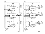
(1)
本発明の一態様は、第1トランジスタと、第2トランジスタと、第3トランジスタと、第4トランジスタと、第5トランジスタと、第6トランジスタと、第7トランジスタと、第8トランジスタと、第9トランジスタと、第10トランジスタと、第1容量と、第2容量と、第3容量と、第4容量と、を有する、半導体装置である。第1トランジスタの第1ゲートは、第4トランジスタの第1ゲートに電気的に接続され、第1トランジスタのソース又はドレインの一方は、第2トランジスタのソース又はドレインの一方と、第5トランジスタのソース又はドレインの一方と、第8トランジスタのソース又はドレインの一方と、第4容量の第1端子と、に電気的に接続されている。第5トランジスタのソース又はドレインの他方は、第6トランジスタの第1ゲートと、第2容量の第1端子と、に電気的に接続されている。第8トランジスタのソース又はドレインの他方は、第9トランジスタの第1ゲートと、第3容量の第1端子と、に電気的に接続されている。第2トランジスタの第1ゲートは、第1容量の第1端子と、第3トランジスタのソース又はドレインの一方と、第4トランジスタのソース又はドレインの一方と、第7トランジスタの第1ゲートと、第10トランジスタの第1ゲートと、に電気的に接続されている。第7トランジスタのソース又はドレインの一方は、第6トランジスタのソース又はドレインの一方と、第2容量の第2端子と、に電気的に接続されている。第10トランジスタのソース又はドレインの一方は、第9トランジスタのソース又はドレインの一方と、第3容量の第2端子と、に電気的に接続されている。
(1)
One embodiment of the present invention includes a first transistor, a second transistor, a third transistor, a fourth transistor, a fifth transistor, a sixth transistor, a seventh transistor, an eighth transistor, and a ninth transistor. , a tenth transistor, a first capacitor, a second capacitor, a third capacitor, and a fourth capacitor. A first gate of the first transistor is electrically connected to a first gate of the fourth transistor, and one of the source or drain of the first transistor is connected to one of the source or drain of the second transistor and the source of the fifth transistor. Alternatively, it is electrically connected to one of the drains, one of the source or drain of the eighth transistor, and the first terminal of the fourth capacitor. The other of the source or drain of the fifth transistor is electrically connected to the first gate of the sixth transistor and the first terminal of the second capacitor. The other of the source or drain of the eighth transistor is electrically connected to the first gate of the ninth transistor and the first terminal of the third capacitor. The first gate of the second transistor includes the first terminal of the first capacitor, one of the source or drain of the third transistor, one of the source or drain of the fourth transistor, the first gate of the seventh transistor, and the first gate of the third transistor. 10 is electrically connected to the first gate of the transistor. One of the source or drain of the seventh transistor is electrically connected to one of the source or drain of the sixth transistor and the second terminal of the second capacitor. One of the source or drain of the tenth transistor is electrically connected to one of the source or drain of the ninth transistor and the second terminal of the third capacitor.
(2)
又は、本発明の一態様は、第1トランジスタと、第2トランジスタと、第3トランジスタと、第4トランジスタと、第5トランジスタと、第6トランジスタと、第7トランジスタと、第8トランジスタと、第9トランジスタと、第10トランジスタと、第11トランジスタと、第1容量と、第2容量と、第3容量と、を有する、半導体装置である。第1トランジスタの第1ゲートは、第11トランジスタのソース又はドレインの一方に電気的に接続され、第11トランジスタのソース又はドレインの他方は、第4トランジスタの第1ゲートに電気的に接続されている。第1トランジスタのソース又はドレインの一方は、第2トランジスタのソース又はドレインの一方と、第5トランジスタのソース又はドレインの一方と、第8トランジスタのソース又はドレインの一方と、に電気的に接続されている。第5トランジスタのソース又はドレインの他方は、第6トランジスタの第1ゲートと、第2容量の第1端子と、に電気的に接続されている。第8トランジスタのソース又はドレインの他方は、第9トランジスタの第1ゲートと、第3容量の第1端子と、に電気的に接続されている。第2トランジスタの第1ゲートは、第1容量の第1端子と、第3トランジスタのソース又はドレインの一方と、第4トランジスタのソース又はドレインの一方と、第7トランジスタの第1ゲートと、第10トランジスタの第1ゲートと、に電気的に接続されている。第7トランジスタのソース又はドレインの一方は、第6トランジスタのソース又はドレインの一方と、第2容量の第2端子と、に電気的に接続されている。第10トランジスタのソース又はドレインの一方は、第9トランジスタのソース又はドレインの一方と、第3容量の第2端子と、に電気的に接続されている。
(2)
Alternatively, one embodiment of the present invention includes a first transistor, a second transistor, a third transistor, a fourth transistor, a fifth transistor, a sixth transistor, a seventh transistor, an eighth transistor, and a third transistor. The semiconductor device includes nine transistors, a tenth transistor, an eleventh transistor, a first capacitor, a second capacitor, and a third capacitor. The first gate of the first transistor is electrically connected to one of the source and drain of the eleventh transistor, and the other of the source and drain of the eleventh transistor is electrically connected to the first gate of the fourth transistor. there is One of the source or drain of the first transistor is electrically connected to one of the source or drain of the second transistor, one of the source or drain of the fifth transistor, and one of the source or drain of the eighth transistor. ing. The other of the source or drain of the fifth transistor is electrically connected to the first gate of the sixth transistor and the first terminal of the second capacitor. The other of the source or drain of the eighth transistor is electrically connected to the first gate of the ninth transistor and the first terminal of the third capacitor. The first gate of the second transistor includes the first terminal of the first capacitor, one of the source or drain of the third transistor, one of the source or drain of the fourth transistor, the first gate of the seventh transistor, and the first gate of the third transistor. 10 is electrically connected to the first gate of the transistor. One of the source or drain of the seventh transistor is electrically connected to one of the source or drain of the sixth transistor and the second terminal of the second capacitor. One of the source or drain of the tenth transistor is electrically connected to one of the source or drain of the ninth transistor and the second terminal of the third capacitor.
(3)
又は、本発明の一態様は、上記(2)において、第11トランジスタの第1ゲートが第11トランジスタの第2ゲートに電気的に接続されている構成としてもよい。
(3)
Alternatively, according to one embodiment of the present invention, in (2) above, the first gate of the eleventh transistor may be electrically connected to the second gate of the eleventh transistor.
(4)
又は、本発明の一態様は、第1トランジスタと、第2トランジスタと、第3トランジスタと、第4トランジスタと、第5トランジスタと、第6トランジスタと、第7トランジスタと、第8トランジスタと、第9トランジスタと、第10トランジスタと、第11トランジスタと、第12トランジスタと、第1容量と、第2容量と、第3容量と、を有する、半導体装置である。第1トランジスタの第1ゲートは、第11トランジスタのソース又はドレインの一方と、第12トランジスタのソース又はドレインの一方と、に電気的に接続され、第11トランジスタのソース又はドレインの他方は、第11トランジスタの第1ゲートと、第4トランジスタの第1ゲートと、第12トランジスタのソース又はドレインの他方と、に電気的に接続されている。第1トランジスタのソース又はドレインの一方は、第2トランジスタのソース又はドレインの一方と、第5トランジスタのソース又はドレインの一方と、第8トランジスタのソース又はドレインの一方と、に電気的に接続されている。第5トランジスタのソース又はドレインの他方は、第6トランジスタの第1ゲートと、第2容量の第1端子と、に電気的に接続されている。第8トランジスタのソース又はドレインの他方は、第9トランジスタの第1ゲートと、第3容量の第1端子と、に電気的に接続されている。第2トランジスタの第1ゲートは、第1容量の第1端子と、第3トランジスタのソース又はドレインの一方と、第4トランジスタのソース又はドレインの一方と、第7トランジスタの第1ゲートと、第10トランジスタの第1ゲートと、に電気的に接続されている。第7トランジスタのソース又はドレインの一方は、第6トランジスタのソース又はドレインの一方と、第2容量の第2端子と、に電気的に接続されている。第10トランジスタのソース又はドレインの一方は、第9トランジスタのソース又はドレインの一方と、第3容量の第2端子と、に電気的に接続されている。第6トランジスタのソース又はドレインの他方は、第12トランジスタの第1ゲートに電気的に接続されている。
(4)
Alternatively, one embodiment of the present invention includes a first transistor, a second transistor, a third transistor, a fourth transistor, a fifth transistor, a sixth transistor, a seventh transistor, an eighth transistor, and a third transistor. The semiconductor device includes nine transistors, a tenth transistor, an eleventh transistor, a twelfth transistor, a first capacitor, a second capacitor, and a third capacitor. The first gate of the first transistor is electrically connected to one of the source or drain of the eleventh transistor and one of the source or drain of the twelfth transistor, and the other of the source or drain of the eleventh transistor is electrically connected to the The first gate of the 11th transistor, the first gate of the fourth transistor, and the other of the source or drain of the 12th transistor are electrically connected. One of the source or drain of the first transistor is electrically connected to one of the source or drain of the second transistor, one of the source or drain of the fifth transistor, and one of the source or drain of the eighth transistor. ing. The other of the source or drain of the fifth transistor is electrically connected to the first gate of the sixth transistor and the first terminal of the second capacitor. The other of the source or drain of the eighth transistor is electrically connected to the first gate of the ninth transistor and the first terminal of the third capacitor. The first gate of the second transistor includes the first terminal of the first capacitor, one of the source or drain of the third transistor, one of the source or drain of the fourth transistor, the first gate of the seventh transistor, and the first gate of the third transistor. 10 is electrically connected to the first gate of the transistor. One of the source or drain of the seventh transistor is electrically connected to one of the source or drain of the sixth transistor and the second terminal of the second capacitor. One of the source or drain of the tenth transistor is electrically connected to one of the source or drain of the ninth transistor and the second terminal of the third capacitor. The other of the source or drain of the sixth transistor is electrically connected to the first gate of the twelfth transistor.
(5)
又は、本発明の一態様は、上記(1)乃至(4)のいずれか一において、第5トランジスタの第1ゲートが第5トランジスタの第2ゲートに電気的に接続され、第8トランジスタの第1ゲートが第8トランジスタの第2ゲートに電気的に接続されている構成としてもよい。
(5)
Alternatively, in one embodiment of the present invention, in any one of (1) to (4) above, the first gate of the fifth transistor is electrically connected to the second gate of the fifth transistor, and the A configuration in which one gate is electrically connected to the second gate of the eighth transistor may be employed.
(6)
又は、本発明の一態様は、第1トランジスタと、第2トランジスタと、第3トランジスタと、第4トランジスタと、第5トランジスタと、第6トランジスタと、第7トランジスタと、第8トランジスタと、第9トランジスタと、第10トランジスタと、第1容量と、第2容量と、第3容量と、を有する、半導体装置である。第1トランジスタの第1ゲートは、第4トランジスタの第1ゲートに電気的に接続され、第1トランジスタのソース又はドレインの一方は、第2トランジスタのソース又はドレインの一方と、第5トランジスタのソース又はドレインの一方と、第8トランジスタのソース又はドレインの一方と、に電気的に接続されている。第5トランジスタのソース又はドレインの他方は、第6トランジスタの第1ゲートと、第2容量の第1端子と、に電気的に接続されている。第8トランジスタのソース又はドレインの他方は、第9トランジスタの第1ゲートと、第3容量の第1端子と、に電気的に接続されている。第2トランジスタの第1ゲートは、第1容量の第1端子と、第3トランジスタのソース又はドレインの一方と、第4トランジスタのソース又はドレインの一方と、第7トランジスタの第1ゲートと、第10トランジスタの第1ゲートと、第5トランジスタの第2ゲートと、第8トランジスタの第2ゲートと、に電気的に接続されている。第7トランジスタのソース又はドレインの一方は、第6トランジスタのソース又はドレインの一方と、第2容量の第2端子と、に電気的に接続されている。第10トランジスタのソース又はドレインの一方は、第9トランジスタのソース又はドレインの一方と、第3容量の第2端子と、に電気的に接続されている。
(6)
Alternatively, one embodiment of the present invention includes a first transistor, a second transistor, a third transistor, a fourth transistor, a fifth transistor, a sixth transistor, a seventh transistor, an eighth transistor, and a third transistor. The semiconductor device includes nine transistors, a tenth transistor, a first capacitor, a second capacitor, and a third capacitor. A first gate of the first transistor is electrically connected to a first gate of the fourth transistor, and one of the source or drain of the first transistor is connected to one of the source or drain of the second transistor and the source of the fifth transistor. or electrically connected to one of the drains and one of the source or drain of the eighth transistor. The other of the source or drain of the fifth transistor is electrically connected to the first gate of the sixth transistor and the first terminal of the second capacitor. The other of the source or drain of the eighth transistor is electrically connected to the first gate of the ninth transistor and the first terminal of the third capacitor. The first gate of the second transistor includes the first terminal of the first capacitor, one of the source or drain of the third transistor, one of the source or drain of the fourth transistor, the first gate of the seventh transistor, and the first gate of the third transistor. 10 transistor, the second gate of the fifth transistor, and the second gate of the eighth transistor. One of the source or drain of the seventh transistor is electrically connected to one of the source or drain of the sixth transistor and the second terminal of the second capacitor. One of the source or drain of the tenth transistor is electrically connected to one of the source or drain of the ninth transistor and the second terminal of the third capacitor.
(7)
又は、本発明の一態様は、第1トランジスタと、第2トランジスタと、第3トランジスタと、第4トランジスタと、第6トランジスタと、第7トランジスタと、第9トランジスタと、第10トランジスタと、第1容量と、第2容量と、第3容量と、を有する、半導体装置である。第1トランジスタの第1ゲートは、第4トランジスタの第1ゲートに電気的に接続され、第1トランジスタのソース又はドレインの一方は、第2トランジスタのソース又はドレインの一方と、第6トランジスタの第1ゲートと、第2容量の第1端子と、第9トランジスタの第1ゲートと、第3容量の第1端子と、に電気的に接続されている。第2トランジスタの第1ゲートは、第1容量の第1端子と、第3トランジスタのソース又はドレインの一方と、第4トランジスタのソース又はドレインの一方と、第7トランジスタの第1ゲートと、第10トランジスタの第1ゲートと、に電気的に接続されている。第7トランジスタのソース又はドレインの一方は、第6トランジスタのソース又はドレインの一方と、第2容量の第2端子と、に電気的に接続されている。第10トランジスタのソース又はドレインの一方は、第9トランジスタのソース又はドレインの一方と、第3容量の第2端子と、に電気的に接続されている。
(7)
Alternatively, one embodiment of the present invention includes a first transistor, a second transistor, a third transistor, a fourth transistor, a sixth transistor, a seventh transistor, a ninth transistor, a tenth transistor, and a third transistor. A semiconductor device having a first capacitor, a second capacitor, and a third capacitor. A first gate of the first transistor is electrically connected to a first gate of the fourth transistor, one of the source or drain of the first transistor is connected to one of the source or drain of the second transistor, and the other of the source or drain of the sixth transistor. 1 gate, the first terminal of the second capacitor, the first gate of the ninth transistor, and the first terminal of the third capacitor. The first gate of the second transistor includes the first terminal of the first capacitor, one of the source or drain of the third transistor, one of the source or drain of the fourth transistor, the first gate of the seventh transistor, and the first gate of the third transistor. 10 is electrically connected to the first gate of the transistor. One of the source or drain of the seventh transistor is electrically connected to one of the source or drain of the sixth transistor and the second terminal of the second capacitor. One of the source or drain of the tenth transistor is electrically connected to one of the source or drain of the ninth transistor and the second terminal of the third capacitor.
(8)
又は、本発明の一態様は、上記(1)乃至(7)のいずれか一において、第1トランジスタの第1ゲートが第1トランジスタの第2ゲートに電気的に接続され、第3トランジスタの第1ゲートが第3トランジスタの第2ゲートに電気的に接続され、第6トランジスタの第1ゲートが第6トランジスタの第2ゲートに電気的に接続され、第9トランジスタの第1ゲートが第9トランジスタの第2ゲートに電気的に接続されている構成としてもよい。
(8)
Alternatively, in one embodiment of the present invention, in any one of (1) to (7) above, the first gate of the first transistor is electrically connected to the second gate of the first transistor, and the second gate of the third transistor is electrically connected to the second gate of the first transistor. 1 gate electrically connected to the second gate of the third transistor; the first gate of the sixth transistor electrically connected to the second gate of the sixth transistor; and the first gate of the ninth transistor to the ninth transistor. may be electrically connected to the second gate of .
(9)
又は、本発明の一態様は、上記(1)乃至(8)のいずれか一において、第7トランジスタの第2ゲートが第7トランジスタのソース又はドレインの他方に電気的に接続され、第10トランジスタの第2ゲートが第10トランジスタのソース又はドレインの他方に電気的に接続されている構成としてもよい。
(9)
Alternatively, according to one embodiment of the present invention, in any one of (1) to (8) above, the second gate of the seventh transistor is electrically connected to the other of the source and the drain of the seventh transistor, and the tenth transistor may be electrically connected to the other of the source and drain of the tenth transistor.
(10)
又は、本発明の一態様は、上記(1)乃至(9)のいずれか一において、第2トランジスタ、及び第4トランジスタのそれぞれがマルチゲート構造のトランジスタとなっている構成としてもよい。
(10)
Alternatively, in one embodiment of the present invention, in any one of (1) to (9), each of the second transistor and the fourth transistor may have a multi-gate structure.
(11)
又は、本発明の一態様は、上記(1)乃至(10)のいずれか一の半導体装置を含むシフトレジスタを有するゲートドライバ回路と、ソースドライバ回路と、画素アレイと、を有する、表示装置である。
(11)
Alternatively, one embodiment of the present invention is a display device including a gate driver circuit including a shift register including the semiconductor device according to any one of (1) to (10), a source driver circuit, and a pixel array. be.
(12)
又は、本発明の一態様は、上記(11)の表示装置と、筐体と、を有する、電子機器である。
(12)
Alternatively, one embodiment of the present invention is an electronic device including the display device of (11) and a housing.
なお、本明細書等において、半導体装置とは、半導体特性を利用した装置であり、半導体素子(例えば、トランジスタ、ダイオード、及びフォトダイオード)を含む回路、同回路を有する装置等をいう。また、半導体特性を利用することで機能しうる装置全般をいう。例えば、集積回路、集積回路を備えたチップ、及びパッケージにチップを収納した電子部品のそれぞれは半導体装置の一例である。また、記憶装置、表示装置、発光装置、照明装置及び電子機器は、それ自体が半導体装置である場合があり、半導体装置を有している場合がある。 Note that in this specification and the like, a semiconductor device is a device that utilizes semiconductor characteristics and refers to a circuit including a semiconductor element (eg, a transistor, a diode, and a photodiode), a device including the circuit, and the like. It also refers to all devices that can function by utilizing semiconductor characteristics. For example, an integrated circuit, a chip including the integrated circuit, and an electronic component containing the chip in a package are examples of semiconductor devices. In addition, memory devices, display devices, light-emitting devices, lighting devices, and electronic devices themselves may be semiconductor devices or may include semiconductor devices.
また、本明細書等において、XとYとが接続されていると記載されている場合は、XとYとが電気的に接続されている場合と、XとYとが機能的に接続されている場合と、XとYとが直接接続されている場合とが、本明細書等に開示されているものとする。したがって、所定の接続関係、例えば、図又は文章に示された接続関係に限定されず、図又は文章に示された接続関係以外のものも、図又は文章に開示されているものとする。X、Yは、対象物(例えば、装置、素子、回路、配線、電極、端子、導電膜、及び層)であるとする。 In addition, in this specification and the like, when it is described that X and Y are connected, it means that X and Y are electrically connected and that X and Y are functionally connected. This specification and the like disclose a case where X and Y are directly connected and a case where X and Y are directly connected. Therefore, it is assumed that the connection relationships other than the connection relationships shown in the drawings or the text are not limited to the predetermined connection relationships, for example, the connection relationships shown in the drawings or the text. Let X and Y be objects (eg, devices, elements, circuits, wiring, electrodes, terminals, conductive films, and layers).
XとYとが電気的に接続されている場合の一例としては、XとYとの電気的な接続を可能とする素子(例えば、スイッチ、トランジスタ、容量素子、インダクタ、抵抗素子、ダイオード、表示デバイス、発光デバイス、及び負荷)が、XとYとの間に1個以上接続されることが可能である。なお、スイッチは、オンオフが制御される機能を有している。つまり、スイッチは、導通状態(オン状態)、又は、非導通状態(オフ状態)になり、電流を流すか流さないかを制御する機能を有している。 An example of the case where X and Y are electrically connected is an element that enables electrical connection between X and Y (for example, switch, transistor, capacitive element, inductor, resistive element, diode, display devices, light emitting devices, and loads) can be connected between X and Y one or more times. Note that the switch has a function of being controlled to be turned on and off. In other words, the switch has the function of being in a conducting state (on state) or a non-conducting state (off state) and controlling whether or not to allow current to flow.
なお、XとYとの間に、素子と電源線(例えば、VDD(高電源電位)、VSS(低電源電位)、GND(接地電位)、又は所望の電位を与える配線)との両方が配置されている場合には、XとYとが電気的に接続されている、とは規定しないものとする。なお、XとYとの間に電源線のみが配置されている場合には、XとYとの間に別の素子がないため、XとYとは、直接接続されている、ということになる。よって、XとYとの間に、電源線のみが配置されている場合には、「XとYとは、電気的に接続されている」ともいえる。しかし、XとYとの間に、素子と電源線の両方が配置されている場合には、Xと電源線とが(素子を介して)電気的に接続されており、Yと電源線とが電気的に接続されている、ということになるが、XとYとは、電気的に接続されている、とは規定されない。なお、例えば、Xとトランジスタのゲートとが電気的に接続され、Yと当該トランジスタのソースとが電気的に接続されている場合、XとYとが電気的に接続されている、とは規定しないものとする。また、Xとトランジスタのゲートとが電気的に接続され、Yと当該トランジスタのドレインとが電気的に接続されている場合、XとYとが電気的に接続されている、とは規定しないものとする。また、例えば、Xとトランジスタのドレインとが電気的に接続され、Yと当該トランジスタのソースとが電気的に接続されている場合、XとYとが電気的に接続されている、と規定するものとする。なお、XとYとの間に、容量素子が配置されている場合には、XとYとが電気的に接続されている、と規定する場合と規定しない場合がある。例えば、デジタル回路又はロジック回路の構成において、XとYとの間に、容量素子が配置されている場合には、XとYとが電気的に接続されている、とは規定しない場合がある。一方、例えば、アナログ回路の構成において、XとYとの間に、容量素子が配置されている場合には、XとYとが電気的に接続されている、と規定する場合がある。 Between X and Y, both an element and a power supply line (for example, VDD (high power supply potential), VSS (low power supply potential), GND (ground potential), or a wiring that gives a desired potential) are arranged. It shall not be defined that X and Y are electrically connected when they are connected. In addition, when only a power supply line is arranged between X and Y, since there is no other element between X and Y, X and Y are directly connected. Become. Therefore, when only a power supply line is arranged between X and Y, it can be said that "X and Y are electrically connected." However, when both the element and the power supply line are arranged between X and Y, X and the power supply line are electrically connected (via the element), and Y and the power supply line are connected. are electrically connected, but it is not defined that X and Y are electrically connected. Note that, for example, when X is electrically connected to the gate of a transistor and Y is electrically connected to the source of the transistor, it is not defined that X and Y are electrically connected. shall not. In addition, when X is electrically connected to the gate of a transistor and Y is electrically connected to the drain of the transistor, it is not defined that X and Y are electrically connected. and Further, for example, when X is electrically connected to the drain of a transistor, and Y is electrically connected to the source of the transistor, it is defined that X and Y are electrically connected. shall be Note that when a capacitive element is arranged between X and Y, it may or may not be defined that X and Y are electrically connected. For example, in the configuration of a digital circuit or logic circuit, if a capacitive element is arranged between X and Y, it may not be defined that X and Y are electrically connected. . On the other hand, for example, in the configuration of an analog circuit, when a capacitive element is arranged between X and Y, X and Y may be defined as being electrically connected.
XとYとが機能的に接続されている場合の一例としては、XとYとの機能的な接続を可能とする回路(例えば、論理回路(例えば、インバータ、NAND回路、及びNOR回路)、信号変換回路(例えば、デジタルアナログ変換回路、アナログデジタル変換回路、及びガンマ補正回路)、電位レベル変換回路(例えば、昇圧回路又は降圧回路といった電源回路、及び信号の電位レベルを変えるレベルシフタ回路)、電圧源、電流源、切り替え回路、増幅回路(例えば、信号振幅又は電流量などを大きくできる回路、オペアンプ、差動増幅回路、ソースフォロワ回路、及びバッファ回路)、信号生成回路、記憶回路、及び制御回路)が、XとYとの間に1個以上接続されることが可能である。なお、一例として、XとYとの間に別の回路を挟んでいても、Xから出力された信号がYへ伝達される場合は、XとYとは機能的に接続されているものとする。 An example of the case where X and Y are functionally connected is a circuit that enables functional connection between X and Y (e.g., logic circuit (e.g., inverter, NAND circuit, and NOR circuit), Signal conversion circuits (e.g., digital-to-analog conversion circuits, analog-to-digital conversion circuits, and gamma correction circuits), potential level conversion circuits (e.g., power supply circuits such as step-up circuits or step-down circuits, and level shifter circuits that change the potential level of signals), voltage source, current source, switching circuit, amplifier circuit (for example, a circuit that can increase signal amplitude or current amount, operational amplifier, differential amplifier circuit, source follower circuit, and buffer circuit), signal generation circuit, memory circuit, and control circuit ) can be connected between X and Y one or more times. As an example, even if another circuit is interposed between X and Y, when a signal output from X is transmitted to Y, X and Y are considered to be functionally connected. do.
なお、XとYとが電気的に接続されている、と明示的に記載する場合は、XとYとが電気的に接続されている場合(つまり、XとYとの間に別の素子又は別の回路を挟んで接続されている場合)と、XとYとが直接接続されている場合(つまり、XとYとの間に別の素子又は別の回路を挟まずに接続されている場合)と、を含むものとする。 It should be noted that when explicitly describing that X and Y are electrically connected, it means that X and Y are electrically connected (that is, another element or another circuit is interposed), and the case where X and Y are directly connected (that is, the case where X and Y are connected without another element or another circuit interposed between them). (if any) and
また、例えば、「XとYとトランジスタのソース(第1の端子又は第2の端子の一方に言い換える場合がある)とドレイン(第1の端子又は第2の端子の他方に言い換える場合がある)とは、互いに電気的に接続されており、X、トランジスタのソース、トランジスタのドレイン、Yの順序で電気的に接続されている。」と表現することができる。又は、「トランジスタのソースは、Xと電気的に接続され、トランジスタのドレインはYと電気的に接続され、X、トランジスタのソース、トランジスタのドレイン、Yは、この順序で電気的に接続されている」と表現することができる。又は、「Xは、トランジスタのソースとドレインとを介して、Yと電気的に接続され、X、トランジスタのソース、トランジスタのドレイン、Yは、この接続順序で設けられている」と表現することができる。これらの例と同様な表現方法を用いて、回路構成における接続の順序について規定することにより、トランジスタのソースと、ドレインとを、区別して、技術的範囲を決定することができる。なお、これらの表現方法は、一例であり、これらの表現方法に限定されない。ここで、X、Yは、対象物(例えば、装置、素子、回路、配線、電極、端子、導電膜、又は層)であるとする。 Also, for example, "X and Y, and the source of the transistor (which may be referred to as either the first terminal or the second terminal) and the drain (which may be referred to as the other of the first terminal or the second terminal) are electrically connected to each other in the order of X, the source of the transistor, the drain of the transistor, and Y.". Or, "The source of the transistor is electrically connected to X, the drain of the transistor is electrically connected to Y, and X, the source of the transistor, the drain of the transistor, Y are electrically connected in that order. It can be expressed as Alternatively, the expression "X is electrically connected to Y through the source and drain of the transistor, and X, the source of the transistor, the drain of the transistor, and Y are provided in this connection order." can be done. By defining the order of connection in the circuit configuration using a method of expression similar to these examples, the source and drain of the transistor can be distinguished and the technical scope can be determined. In addition, these expression methods are examples, and are not limited to these expression methods. Here, X and Y are objects (for example, devices, elements, circuits, wiring, electrodes, terminals, conductive films, or layers).
なお、回路図上は独立している構成要素同士が電気的に接続しているように図示されている場合であっても、1つの構成要素が、複数の構成要素の機能を併せ持っている場合もある。例えば配線の一部が電極としても機能する場合は、一の導電膜が、配線の機能、及び電極の機能の両方の構成要素の機能を併せ持っている。したがって、本明細書における電気的に接続とは、このような、一の導電膜が、複数の構成要素の機能を併せ持っている場合も、その範疇に含める。 Even if the circuit diagram shows independent components electrically connected to each other, if one component has the functions of multiple components There is also For example, when a part of the wiring also functions as an electrode, one conductive film has both the function of the wiring and the function of the electrode. Therefore, the term "electrically connected" in this specification includes cases where one conductive film functions as a plurality of constituent elements.
また、本明細書等において、「抵抗素子」とは、例えば、0Ωよりも高い抵抗値を有する回路素子、又は、0Ωよりも高い抵抗値を有する配線とすることができる。そのため、本明細書等において、「抵抗素子」は、抵抗値を有する配線、ソース-ドレイン間に電流が流れるトランジスタ、ダイオード、コイルなどを含むものとする。そのため、「抵抗素子」という用語は、「抵抗」、「負荷」、又は「抵抗値を有する領域」の用語に言い換えることができる場合がある。逆に「抵抗」、「負荷」、又は「抵抗値を有する領域」といった用語は、「抵抗素子」という用語に言い換えることができる場合がある。抵抗値としては、例えば、好ましくは1mΩ以上10Ω以下、より好ましくは5mΩ以上5Ω以下、更に好ましくは10mΩ以上1Ω以下とすることができる。また、例えば、1Ω以上1×10⁹Ω以下としてもよい。 Further, in this specification and the like, a “resistive element” can be, for example, a circuit element having a resistance value higher than 0Ω, or a wiring having a resistance value higher than 0Ω. Therefore, in this specification and the like, the term “resistive element” includes a wiring having a resistance value, a transistor, a diode, a coil, and the like through which current flows between the source and the drain. Therefore, the term "resistive element" may be interchanged with the terms "resistance", "load", or "region having a resistance value". Conversely, terms such as "resistor", "load", or "region having a resistance value" may be interchanged with the term "resistive element". The resistance value can be, for example, preferably 1 mΩ or more and 10Ω or less, more preferably 5 mΩ or more and 5 Ω or less, still more preferably 10 mΩ or more and 1 Ω or less. Also, for example, it may be 1 Ω or more and 1×10 9 Ω or less.
また、本明細書等において、「容量素子」とは、例えば、0Fよりも高い静電容量の値を有する回路素子、0Fよりも高い静電容量の値を有する配線の領域、寄生容量、又はトランジスタのゲート容量とすることができる。また、「容量素子」、「寄生容量」、又は「ゲート容量」という用語は、「容量」という用語に言い換えることができる場合がある。逆に、「容量」という用語は、「容量素子」、「寄生容量」、「ゲート容量」といった用語に言い換えることができる場合がある。また、「容量」の「一対の電極」という用語は、「一対の導電体」、「一対の導電領域」、又は「一対の領域」に言い換えることができる。なお、静電容量の値としては、例えば、0.05fF以上10pF以下とすることができる。また、例えば、1pF以上10μF以下としてもよい。 In this specification and the like, the term “capacitance element” refers to, for example, a circuit element having a capacitance value higher than 0 F, a wiring region having a capacitance value higher than 0 F, a parasitic capacitance, or It can be the gate capacitance of a transistor. Also, the terms “capacitance element”, “parasitic capacitance”, or “gate capacitance” may be interchanged with the term “capacitance”. Conversely, the term "capacitance" may be interchanged with terms such as "capacitance element," "parasitic capacitance," and "gate capacitance." Also, the term "a pair of electrodes" in the "capacitance" can be replaced with a "pair of conductors," a "pair of conductive regions," or a "pair of regions." Note that the value of the capacitance can be, for example, 0.05 fF or more and 10 pF or less. Also, for example, it may be 1 pF or more and 10 μF or less.
また、本明細書等において、トランジスタは、ゲート、ソース、及びドレインと呼ばれる3つの端子を有する。ゲートは、トランジスタの導通状態を制御する制御端子である。ソース又はドレインとして機能する2つの端子は、トランジスタの入出力端子である。2つの入出力端子は、トランジスタの導電型(nチャネル型、pチャネル型)及びトランジスタの3つの端子に与えられる電位の高低によって、一方がソースとなり他方がドレインとなる。このため、本明細書等においては、ソース、又はドレインの用語は、互いに言い換えることができる場合がある。また、本明細書等では、トランジスタの接続関係を説明する際、「ソース又はドレインの一方」(又は第1電極、又は第1端子)、「ソース又はドレインの他方」(又は第2電極、又は第2端子)という表記を用いる。なお、トランジスタの構造によっては、上述した3つの端子に加えて、バックゲートを有する場合がある。この場合、本明細書等において、トランジスタのゲート又はバックゲートの一方を第1ゲートと呼称し、トランジスタのゲート又はバックゲートの他方を第2ゲートと呼称することがある。更に、同じトランジスタにおいて、「ゲート」と「バックゲート」の用語は互いに入れ換えることができる場合がある。また、トランジスタが、3以上のゲートを有する場合は、本明細書等においては、それぞれのゲートを第1ゲート、第2ゲート、第3ゲートなどと呼称することがある。 In this specification and the like, a transistor has three terminals called a gate, a source, and a drain. A gate is a control terminal that controls the conduction state of a transistor. The two terminals functioning as source or drain are the input and output terminals of the transistor. One of the two input/output terminals functions as a source and the other as a drain depending on the conductivity type of the transistor (n-channel type, p-channel type) and the level of potentials applied to the three terminals of the transistor. Therefore, the terms "source" and "drain" can be used interchangeably in this specification and the like. Further, in this specification and the like, when describing the connection relationship of a transistor, “one of the source or the drain” (or the first electrode, or the first terminal), “the other of the source or the drain” (or the second electrode, or the second terminal) is used. Note that a transistor may have a back gate in addition to the three terminals described above, depending on the structure of the transistor. In this case, in this specification and the like, one of the gate and back gate of the transistor may be referred to as a first gate, and the other of the gate and back gate of the transistor may be referred to as a second gate. Further, the terms "gate" and "backgate" may be used interchangeably for the same transistor. In addition, when a transistor has three or more gates, the respective gates may be referred to as a first gate, a second gate, a third gate, or the like in this specification and the like.
例えば、本明細書等において、トランジスタの一例としては、ゲート電極が2個以上のマルチゲート構造のトランジスタを用いることができる。マルチゲート構造にすると、チャネル形成領域が直列に接続されるため、複数のトランジスタが直列に接続された構造となる。よって、マルチゲート構造により、オフ電流の低減、トランジスタの耐圧向上(信頼性の向上)を図ることができる。または、マルチゲート構造により、飽和領域で動作する時に、ドレインとソースとの間の電圧が変化しても、ドレインとソースとの間の電流があまり変化せず、傾きがフラットである電圧・電流特性を得ることができる。傾きがフラットである電圧・電流特性を利用すると、理想的な電流源回路、又は非常に高い抵抗値をもつ能動負荷を実現することができる。その結果、特性のよい差動回路又はカレントミラー回路などを実現することができる。 For example, in this specification and the like, a multi-gate transistor having two or more gate electrodes can be used as an example of a transistor. In the multi-gate structure, since the channel formation regions are connected in series, a structure in which a plurality of transistors are connected in series is obtained. Therefore, the multi-gate structure can reduce off-state current and improve the breakdown voltage (reliability) of the transistor. Alternatively, due to the multi-gate structure, even if the voltage between the drain and source changes when operating in the saturation region, the current between the drain and source does not change much and the slope is flat. properties can be obtained. By using the flat-slope voltage-current characteristic, an ideal current source circuit or an active load with a very high resistance value can be realized. As a result, a differential circuit or current mirror circuit with good characteristics can be realized.
また、回路図上では、単一の回路素子が図示されている場合でも、当該回路素子が複数の回路素子を有する場合がある。例えば、回路図上に1個の抵抗が記載されている場合は、2個以上の抵抗が直列に電気的に接続されている場合を含むものとする。また、例えば、回路図上に1個の容量が記載されている場合は、2個以上の容量が並列に電気的に接続されている場合を含むものとする。また、例えば、回路図上に1個のトランジスタが記載されている場合は、2個以上のトランジスタが直列に電気的に接続され、かつそれぞれのトランジスタのゲート同士が電気的に接続されている場合を含むものとする。また、同様に、例えば、回路図上に1個のスイッチが記載されている場合は、当該スイッチが2個以上のトランジスタを有し、2個以上のトランジスタが直列、又は並列に電気的に接続され、それぞれのトランジスタのゲート同士が電気的に接続されている場合を含むものとする。 Moreover, even when a single circuit element is illustrated on the circuit diagram, the circuit element may have a plurality of circuit elements. For example, when one resistor is described on the circuit diagram, it includes the case where two or more resistors are electrically connected in series. Further, for example, the case where one capacitor is described on the circuit diagram includes the case where two or more capacitors are electrically connected in parallel. Further, for example, when one transistor is illustrated in a circuit diagram, two or more transistors are electrically connected in series and the gates of the transistors are electrically connected to each other. shall include Similarly, for example, when one switch is described on the circuit diagram, the switch has two or more transistors, and the two or more transistors are electrically connected in series or in parallel. and the gates of the respective transistors are electrically connected to each other.
また、本明細書等において、ノードは、回路構成、及びデバイス構造に応じて、端子、配線、電極、導電層、導電体、不純物領域等と言い換えることが可能である。また、端子、配線等をノードと言い換えることが可能である。 In this specification and the like, a node can be called a terminal, a wiring, an electrode, a conductive layer, a conductor, an impurity region, or the like depending on the circuit configuration and device structure. Terminals, wirings, and the like can also be called nodes.
また、本明細書等において、「電圧」と「電位」は、適宜言い換えることができる。「電圧」は、基準となる電位からの電位差のことであり、例えば基準となる電位をグラウンド電位(接地電位)とすると、「電圧」を「電位」に言い換えることができる。なお、グラウンド電位は必ずしも0Vを意味するとは限らない。また、電位は相対的なものであり、基準となる電位が変わることによって、配線に与えられる電位、回路などに印加される電位、回路などから出力される電位なども変化する。 In this specification and the like, the terms “voltage” and “potential” can be used interchangeably. “Voltage” is a potential difference from a reference potential. For example, if the reference potential is ground potential, “voltage” can be replaced with “potential”. Note that the ground potential does not necessarily mean 0V. In addition, the potential is relative, and when the reference potential changes, the potential applied to the wiring, the potential applied to the circuit, etc., and the potential output from the circuit etc. also change.
また、本明細書等において、「高レベル電位」、及び「低レベル電位」という用語は、特定の電位を意味するものではない。例えば、2本の配線において、両方とも「高レベル電位を供給する配線として機能する」と記載されていた場合、両方の配線が与えるそれぞれの高レベル電位は、互いに等しくなくてもよい。また、同様に、2本の配線において、両方とも「低レベル電位を供給する配線として機能する」と記載されていた場合、両方の配線が与えるそれぞれの低レベル電位は、互いに等しくなくてもよい。 In this specification and the like, the terms “high-level potential” and “low-level potential” do not mean specific potentials. For example, when two wirings are described as "functioning as wirings supplying high-level potentials", the high-level potentials supplied by both wirings do not have to be equal to each other. Similarly, when two wirings are described as "functioning as wirings that supply low-level potentials", the low-level potentials applied by both wirings need not be equal to each other. .
また、「電流」とは、電荷の移動現象(電気伝導)のことであり、例えば、「正の荷電体の電気伝導が起きている」という記載は、「その逆向きに負の荷電体の電気伝導が起きている」と換言することができる。そのため、本明細書等において、「電流」とは、特に断らない限り、キャリアの移動に伴う電荷の移動現象(電気伝導)をいうものとする。ここでいうキャリアとしては、電子、正孔、アニオン、カチオン、及び錯イオンが挙げられ、電流の流れる系(例えば、半導体、金属、電解液、及び真空中)によってキャリアが異なる。また、配線における「電流の向き」は、正電荷となるキャリアが移動する方向とし、正の電流量で記載する。換言すると、負電荷となるキャリアが移動する方向は、電流の向きと逆の方向となり、負の電流量で表現される。そのため、本明細書等において、電流の正負(又は電流の向き)について断りがない場合、「素子Aから素子Bに電流が流れる」の記載は「素子Bから素子Aに電流が流れる」に言い換えることができるものとする。また、「素子Aに電流が入力される」の記載は「素子Aから電流が出力される」に言い換えることができるものとする。 In addition, "electric current" refers to the movement phenomenon of charge (electrical conduction). For example, the statement "electric conduction occurs in a positive In other words, "electrical conduction is occurring". Therefore, in this specification and the like, unless otherwise specified, the term "electric current" refers to a charge transfer phenomenon (electrical conduction) associated with the movement of carriers. Examples of carriers here include electrons, holes, anions, cations, and complex ions, and the carriers differ depending on the current flow system (eg, semiconductor, metal, electrolyte, and in vacuum). Also, the “direction of current” in the wiring is the direction in which carriers that become positive charges move, and is described as a positive amount of current. In other words, the direction in which the carriers that become negative charges move is the direction opposite to the direction of the current, and is represented by the amount of negative current. Therefore, in this specification and the like, when there is no notice about the positive or negative of the current (or the direction of the current), the description of "current flows from the element A to the element B" should be rephrased as "current flows from the element B to the element A." It shall be possible. Also, the description of "a current is input to the element A" can be rephrased as "a current is output from the element A".
また、本明細書等において、「第1」、「第2」、「第3」という序数詞は、構成要素の混同を避けるために付したものである。従って、構成要素の数を限定するものではない。また、構成要素の順序を限定するものではない。例えば、本明細書等の実施の形態の一において「第1」に言及された構成要素が、他の実施の形態、あるいは特許請求の範囲において「第2」に言及された構成要素とすることもありうる。また例えば、本明細書等の実施の形態の一において「第1」に言及された構成要素を、他の実施の形態、あるいは特許請求の範囲において省略することもありうる。 In this specification and the like, ordinal numbers such as "first", "second", and "third" are added to avoid confusion of constituent elements. Therefore, the number of components is not limited. Also, the order of the components is not limited. For example, the component referred to as "first" in one of the embodiments such as this specification may be the component referred to as "second" in another embodiment or the scope of claims. can also be Further, for example, the component referred to as "first" in one of the embodiments of this specification etc. may be omitted in other embodiments or the scope of claims.
また、本明細書等において、「上に」、及び「下に」といった配置を示す語句は、構成同士の位置関係を、図面を参照して説明するために、便宜上用いている場合がある。また、構成同士の位置関係は、各構成を描写する方向に応じて適宜変化するものである。従って、明細書等で説明した語句に限定されず、状況に応じて適切に言い換えることができる。例えば、「導電体の上面に位置する絶縁体」の表現は、示している図面の向きを180度回転することによって、「導電体の下面に位置する絶縁体」と言い換えることができる。 In this specification and the like, terms such as “above” and “below” may be used for convenience in order to describe the positional relationship between configurations with reference to the drawings. In addition, the positional relationship between the configurations changes appropriately according to the direction in which each configuration is drawn. Therefore, it is not limited to the words and phrases explained in the specification, etc., and can be appropriately rephrased according to the situation. For example, the expression "insulator on the top surface of the conductor" can be rephrased as "insulator on the bottom surface of the conductor" by rotating the orientation of the drawing shown by 180 degrees.
また、「上」、又は「下」の用語は、構成要素の位置関係が直上又は直下で、かつ、直接接していることを限定するものではない。例えば、「絶縁層A上の電極B」の表現であれば、絶縁層Aの上に電極Bが直接接して形成されている必要はなく、絶縁層Aと電極Bとの間に他の構成要素を含むものを除外しない。 In addition, the terms "above" and "below" do not limit the positional relationship of components to be directly above or directly below and in direct contact with each other. For example, the expression “electrode B on insulating layer A” does not require that electrode B be formed on insulating layer A in direct contact with another configuration between insulating layer A and electrode B. Do not exclude those containing elements.
また、本明細書等において、マトリクス状に配置された構成要素、及びその位置関係を説明するために、「行」、及び「列」などの語句を使用する場合がある。また、構成同士の位置関係は、各構成を描写する方向に応じて適宜変化するものである。従って、明細書等で説明した語句に限定されず、状況に応じて適切に言い換えることができる。例えば、「行方向」という表現は、示している図面の向きを90度回転することによって、「列方向」と言い換えることができる場合がある。 In this specification and the like, terms such as “row” and “column” may be used to describe components arranged in a matrix and their positional relationships. In addition, the positional relationship between the configurations changes appropriately according to the direction in which each configuration is drawn. Therefore, it is not limited to the words and phrases explained in the specification, etc., and can be appropriately rephrased according to the situation. For example, the expression "row-wise" may be rephrased as "column-wise" by rotating the orientation of the drawing shown by 90 degrees.
また、本明細書等において、「膜」、及び「層」といった語句は、状況に応じて、互いに入れ替えることが可能である。例えば、「導電層」という用語を、「導電膜」という用語に変更することが可能な場合がある。又は、例えば、「絶縁膜」という用語を、「絶縁層」という用語に変更することが可能な場合がある。又は、場合によっては、又は、状況に応じて、「膜」、及び「層」といった語句を使わずに、別の用語に入れ替えることが可能である。例えば、「導電層」又は「導電膜」という用語を、「導電体」という用語に変更することが可能な場合がある。又は、例えば、「絶縁層」、又は「絶縁膜」という用語を、「絶縁体」という用語に変更することが可能な場合がある。 In this specification and the like, the terms “film” and “layer” can be interchanged depending on the situation. For example, it may be possible to change the term "conductive layer" to the term "conductive film." Or, for example, it may be possible to change the term "insulating film" to the term "insulating layer". Alternatively, the terms "film" and "layer" may be omitted and replaced with other terms as the case may or may be. For example, it may be possible to change the term "conductive layer" or "conductive film" to the term "conductor." Or, for example, it may be possible to change the term "insulating layer" or "insulating film" to the term "insulator".
また、本明細書等において「電極」、「配線」、及び「端子」といった用語は、これらの構成要素を機能的に限定するものではない。例えば、「電極」は「配線」の一部として用いられることがあり、その逆もまた同様である。さらに、「電極」、又は「配線」といった用語は、複数の「電極」、又は「配線」が一体となって形成されている場合なども含む。また、例えば、「端子」は「配線」、又は「電極」の一部として用いられることがあり、その逆もまた同様である。更に、「端子」の用語は、複数の「電極」、「配線」、及び「端子」から選ばれた一以上が一体となって形成されている場合なども含む。そのため、例えば、「電極」は「配線」又は「端子」の一部とすることができ、また、例えば、「端子」は「配線」又は「電極」の一部とすることができる。また、「電極」、「配線」、又は「端子」といった用語は、場合によって、「領域」などの用語に置き換える場合がある。 In addition, the terms “electrode”, “wiring”, and “terminal” in this specification and the like do not functionally limit these constituent elements. For example, an "electrode" may be used as part of a "wiring" and vice versa. Furthermore, the term "electrode" or "wiring" includes the case where a plurality of "electrodes" or "wiring" are integrally formed. Also, for example, a "terminal" may be used as part of a "wiring" or an "electrode", and vice versa. Furthermore, the term "terminal" also includes the case where one or more selected from a plurality of "electrodes", "wirings" and "terminals" are integrally formed. So, for example, an "electrode" can be part of a "wiring" or a "terminal", and a "terminal" can be part of a "wiring" or an "electrode", for example. Also, terms such as "electrode", "wiring", or "terminal" may be replaced with terms such as "region" in some cases.
また、本明細書等において、「配線」、「信号線」、又は「電源線」といった用語は、場合によっては、又は、状況に応じて、互いに入れ替えることが可能である。例えば、「配線」という用語を、「信号線」という用語に変更することが可能な場合がある。また、例えば、「配線」という用語を、「電源線」などの用語に変更することが可能な場合がある。また、その逆も同様で、「信号線」、又は「電源線」といった用語を、「配線」という用語に変更することが可能な場合がある。「電源線」といった用語は、「信号線」の用語に変更することが可能な場合がある。また、その逆も同様で「信号線」といった用語は、「電源線」といった用語に変更することが可能な場合がある。また、配線に印加されている「電位」という用語を、場合によっては、又は、状況に応じて、「信号」という用語に変更することが可能な場合がある。また、その逆も同様で、「信号」という用語は、「電位」という用語に変更することが可能な場合がある。 In this specification and the like, terms such as “wiring”, “signal line”, and “power line” can be interchanged depending on the case or situation. For example, it may be possible to change the term "wiring" to the term "signal line". Also, for example, it may be possible to change the term "wiring" to a term such as "power supply line". Also, vice versa, it may be possible to change the term "signal line" or "power line" to the term "wiring". It may be possible to change the term "power line" to the term "signal line". Also, vice versa, the term "signal line" may be changed to the term "power line". Also, the term "potential" applied to the wiring can be changed to the term "signal" in some cases or depending on the situation. And vice versa, the term "signal" may be changed to the term "potential".
本明細書等において、半導体の不純物とは、例えば、半導体層を構成する主成分以外をいう。例えば、濃度が0.1原子%未満の元素は不純物である。不純物が含まれることにより、例えば、半導体の欠陥準位密度が高くなること、キャリア移動度が低下すること、及び結晶性が低下すること、が起こる場合がある。半導体が酸化物半導体である場合、半導体の特性を変化させる不純物としては、例えば、第1族元素、第2族元素、第13族元素、第14族元素、第15族元素、主成分以外の遷移金属などがあり、特に、例えば、水素(水にも含まれる)、リチウム、ナトリウム、シリコン、ホウ素、リン、炭素、窒素などがある。具体的には、半導体がシリコンである場合、半導体の特性を変化させる不純物としては、例えば、第1族元素、第2族元素、第13族元素、及び第15族元素(但し、酸素、水素は含まない)がある。
In this specification and the like, an impurity of a semiconductor means, for example, other than the main component that constitutes a semiconductor layer. For example, elements with a concentration of less than 0.1 atomic percent are impurities. Inclusion of impurities may cause, for example, an increase in the defect level density of the semiconductor, a decrease in carrier mobility, and a decrease in crystallinity. When the semiconductor is an oxide semiconductor, impurities that change the characteristics of the semiconductor include, for example,
本明細書等において、スイッチとは、導通状態(オン状態)、又は、非導通状態(オフ状態)になり、電流を流すか流さないかを制御する機能を有するものをいう。又は、スイッチとは、電流を流す経路を選択して切り替える機能を有するものをいう。そのため、スイッチは、制御端子とは別に、電流を流す端子を2つ、又は3つ以上有する場合がある。一例としては、電気的なスイッチ、機械的なスイッチなどを用いることができる。つまり、スイッチは、電流を制御できるものであればよく、特定のものに限定されない。 In this specification and the like, a switch has a function of being in a conducting state (on state) or a non-conducting state (off state) and controlling whether or not current flows. Alternatively, a switch has a function of selecting and switching a path through which current flows. Therefore, the switch may have two or more terminals through which current flows, in addition to the control terminal. As an example, an electrical switch, a mechanical switch, or the like can be used. In other words, the switch is not limited to a specific one as long as it can control current.
電気的なスイッチの一例としては、トランジスタ(例えば、バイポーラトランジスタ、MOSトランジスタなど)、ダイオード(例えば、PNダイオード、PINダイオード、ショットキーダイオード、MIM(Metal Insulator Metal)ダイオード、MIS(Metal Insulator Semiconductor)ダイオード、ダイオード接続のトランジスタなど)、又はこれらを組み合わせた論理回路などがある。なお、スイッチとしてトランジスタを用いる場合、トランジスタの「導通状態」とは、例えば、トランジスタのソース電極とドレイン電極が電気的に短絡されているとみなせる状態、又はソース電極とドレイン電極との間に電流を流すことができる状態、をいう。また、トランジスタの「非導通状態」とは、トランジスタのソース電極とドレイン電極が電気的に遮断されているとみなせる状態をいう。なおトランジスタを単なるスイッチとして動作させる場合には、トランジスタの極性(導電型)は特に限定されない。 Examples of electrical switches include transistors (e.g., bipolar transistors, MOS transistors, etc.), diodes (e.g., PN diodes, PIN diodes, Schottky diodes, MIM (Metal Insulator Metal) diodes, MIS (Metal Insulator Semiconductor) diodes. , diode-connected transistors, etc.), or a logic circuit combining these. Note that when a transistor is used as a switch, the “conducting state” of the transistor means, for example, a state in which the source electrode and the drain electrode of the transistor can be considered to be electrically short-circuited, or a state in which a current flows between the source electrode and the drain electrode. It is a state in which it is possible to flow A “non-conducting state” of a transistor means a state in which a source electrode and a drain electrode of the transistor can be considered to be electrically cut off. Note that the polarity (conductivity type) of the transistor is not particularly limited when the transistor is operated as a simple switch.
機械的なスイッチの一例としては、MEMS(マイクロ・エレクトロ・メカニカル・システムズ)技術を用いたスイッチがある。そのスイッチは、機械的に動かすことが可能な電極を有し、その電極が動くことによって、導通と非導通とを制御して動作する。 One example of a mechanical switch is a switch using MEMS (Micro Electro Mechanical Systems) technology. The switch has an electrode that can be moved mechanically, and operates by controlling conduction and non-conduction by moving the electrode.
また、本明細書等において、メタルマスク、またはFMM(ファインメタルマスク、高精細なメタルマスク)を用いて作製されるデバイスをMM(メタルマスク)構造のデバイスと呼称する場合がある。また、本明細書等において、メタルマスク、またはFMMを用いることなく作製されるデバイスをMML(メタルマスクレス)構造のデバイスと呼称する場合がある。 In this specification and the like, a device manufactured using a metal mask or FMM (fine metal mask, high-definition metal mask) is sometimes referred to as a device with an MM (metal mask) structure. In this specification and the like, a device manufactured without using a metal mask or FMM may be referred to as a device with an MML (metal maskless) structure.
なお、本明細書等において、各色の発光デバイス(ここでは青(B)、緑(G)、及び赤(R))で、発光層を作り分ける、または発光層を塗り分ける構造をSBS(Side By Side)構造と呼ぶ場合がある。また、本明細書等において、白色光を発することのできる発光デバイスを白色発光デバイスと呼ぶ場合がある。なお、白色発光デバイスは、着色層(例えば、カラーフィルタ)と組み合わせることで、フルカラー表示の表示装置とすることができる。 In this specification and the like, a structure in which a light-emitting layer is separately formed or a light-emitting layer is separately painted in each color light-emitting device (here, blue (B), green (G), and red (R)) is referred to as SBS (Side By Side) structure. In this specification and the like, a light-emitting device capable of emitting white light is sometimes referred to as a white light-emitting device. Note that the white light-emitting device can be combined with a colored layer (for example, a color filter) to form a full-color display device.
また、発光デバイスは、シングル構造と、タンデム構造とに大別することができる。シングル構造のデバイスは、一対の電極間に1つの発光ユニットを有し、当該発光ユニットは、1以上の発光層を含む構成とすることが好ましい。白色発光を得るには、2以上の発光層の各々の発光が補色の関係となるような発光層を選択すればよい。例えば、第1の発光層の発光色と第2の発光層の発光色を補色の関係になるようにすることで、発光デバイス全体として白色発光する構成を得ることができる。また、発光層を3つ以上有する発光デバイスの場合も同様である。 Further, light-emitting devices can be broadly classified into a single structure and a tandem structure. A single-structure device preferably has one light-emitting unit between a pair of electrodes, and the light-emitting unit preferably includes one or more light-emitting layers. In order to obtain white light emission, it is sufficient to select light-emitting layers such that light emitted from each of the two or more light-emitting layers has a complementary color relationship. For example, by making the luminescent color of the first luminescent layer and the luminescent color of the second luminescent layer have a complementary color relationship, it is possible to obtain a configuration in which the entire light emitting device emits white light. The same applies to light-emitting devices having three or more light-emitting layers.
タンデム構造のデバイスは、一対の電極間に2以上の複数の発光ユニットを有し、各発光ユニットは、1以上の発光層を含む構成とすることが好ましい。白色発光を得るには、複数の発光ユニットの発光層からの光を合わせて白色発光が得られる構成とすればよい。なお、白色発光が得られる構成については、シングル構造の構成と同様である。なお、タンデム構造のデバイスにおいて、複数の発光ユニットの間には、電荷発生層などの中間層を設けると好適である。 A device with a tandem structure preferably has two or more light-emitting units between a pair of electrodes, and each light-emitting unit includes one or more light-emitting layers. In order to obtain white light emission, a structure in which white light emission is obtained by combining light from the light emitting layers of a plurality of light emitting units may be employed. Note that the structure for obtaining white light emission is the same as the structure of the single structure. In the tandem structure device, it is preferable to provide an intermediate layer such as a charge generation layer between the plurality of light emitting units.
また、上述の白色発光デバイス(シングル構造またはタンデム構造)と、SBS構造の発光デバイスと、を比較した場合、SBS構造の発光デバイスは、白色発光デバイスよりも消費電力を低くすることができる。消費電力を低く抑えたい場合は、SBS構造の発光デバイスを用いると好適である。一方で、白色発光デバイスは、製造プロセスがSBS構造の発光デバイスよりも簡単であるため、製造コストを低くすることができる、又は製造歩留まりを高くすることができるため、好適である。 In addition, when comparing the white light emitting device (single structure or tandem structure) and the light emitting device having the SBS structure, the light emitting device having the SBS structure can consume less power than the white light emitting device. If it is desired to keep power consumption low, it is preferable to use a light-emitting device with an SBS structure. On the other hand, the white light emitting device is preferable because the manufacturing process is simpler than that of the SBS structure light emitting device, so that the manufacturing cost can be lowered or the manufacturing yield can be increased.
本明細書において、「平行」とは、二つの直線が-10°以上10°以下の角度で配置されている状態をいう。したがって、-5°以上5°以下の場合も含まれる。また、「略平行」又は「概略平行」とは、二つの直線が-30°以上30°以下の角度で配置されている状態をいう。また、「垂直」とは、二つの直線が80°以上100°以下の角度で配置されている状態をいう。したがって、85°以上95°以下の場合も含まれる。また、「略垂直」又は「概略垂直」とは、二つの直線が60°以上120°以下の角度で配置されている状態をいう。 As used herein, the term “parallel” refers to a state in which two straight lines are arranged at an angle of −10° or more and 10° or less. Therefore, the case of −5° or more and 5° or less is also included. Further, "substantially parallel" or "substantially parallel" means a state in which two straight lines are arranged at an angle of -30° or more and 30° or less. "Perpendicular" means that two straight lines are arranged at an angle of 80° or more and 100° or less. Therefore, the case of 85° or more and 95° or less is also included. Moreover, "substantially perpendicular" or "substantially perpendicular" means a state in which two straight lines are arranged at an angle of 60° or more and 120° or less.
本発明の一態様によって、安定して動作が行われる半導体装置を提供することができる。又は、本発明の一態様によって、信頼性の高い半導体装置を提供することができる。又は、本発明の一態様によって、上述した半導体装置を含む表示装置を提供することができる。又は、本発明の一態様によっては、上述した表示装置を含む電子機器を提供することができる。又は、本発明の一態様によって、新規な半導体装置、新規な表示装置、又は新規な電子機器を提供することができる。 According to one embodiment of the present invention, a semiconductor device that operates stably can be provided. Alternatively, according to one embodiment of the present invention, a highly reliable semiconductor device can be provided. Alternatively, according to one embodiment of the present invention, a display device including any of the above semiconductor devices can be provided. Alternatively, according to one embodiment of the present invention, an electronic device including any of the above display devices can be provided. Alternatively, according to one embodiment of the present invention, a novel semiconductor device, a novel display device, or a novel electronic appliance can be provided.
なお、本発明の一態様の効果は、上記列挙した効果に限定されない。上記列挙した効果は、他の効果の存在を妨げるものではない。なお、他の効果は、以下の記載で述べる、本項目で言及していない効果である。本項目で言及していない効果は、当業者であれば明細書又は図面等の記載から導き出せるものであり、これらの記載から適宜抽出することができる。なお、本発明の一態様は、上記列挙した効果、及び他の効果のうち、少なくとも一つの効果を有するものである。従って本発明の一態様は、場合によっては、上記列挙した効果を有さない場合もある。 Note that the effects of one embodiment of the present invention are not limited to the effects listed above. The effects listed above do not preclude the existence of other effects. Note that other effects are effects not mentioned in this item, which will be described in the following description. Effects not mentioned in this item can be derived from the descriptions in the specification, drawings, etc. by those skilled in the art, and can be appropriately extracted from these descriptions. Note that one embodiment of the present invention has at least one of the effects listed above and other effects. Accordingly, one aspect of the present invention may not have the effects listed above depending on the case.
本明細書等において、金属酸化物(metal oxide)とは、広い意味での金属の酸化物である。金属酸化物は、酸化物絶縁体、酸化物導電体(透明酸化物導電体を含む)、酸化物半導体(Oxide Semiconductor又は単にOSともいう)などに分類される。例えば、トランジスタのチャネル形成領域に金属酸化物が含まれている場合、当該金属酸化物を酸化物半導体と呼称する場合がある。つまり、金属酸化物が、増幅作用、整流作用、及びスイッチング作用から選ばれた1つ以上を有するトランジスタのチャネル形成領域を構成し得る場合、当該金属酸化物を、金属酸化物半導体(metal oxide semiconductor)と呼称することができる。また、OSトランジスタと記載する場合においては、金属酸化物又は酸化物半導体を有するトランジスタと換言することができる。 In this specification and the like, a metal oxide is a metal oxide in a broad sense. Metal oxides are classified into oxide insulators, oxide conductors (including transparent oxide conductors), oxide semiconductors (also referred to as oxide semiconductors or simply OSs), and the like. For example, when a channel formation region of a transistor contains a metal oxide, the metal oxide is sometimes referred to as an oxide semiconductor. That is, when a metal oxide can form a channel-forming region of a transistor having one or more selected from amplifying action, rectifying action, and switching action, the metal oxide is called a metal oxide semiconductor. ). In the case of describing an OS transistor, it can also be referred to as a transistor including a metal oxide or an oxide semiconductor.
また、本明細書等において、窒素を有する金属酸化物も金属酸化物(metal oxide)と総称する場合がある。また、窒素を有する金属酸化物を、金属酸窒化物(metal oxynitride)と呼称してもよい。 In addition, in this specification and the like, metal oxides containing nitrogen may also be collectively referred to as metal oxides. Metal oxides containing nitrogen may also be referred to as metal oxynitrides.
また、本明細書等において、各実施の形態に示す構成は、他の実施の形態に示す構成と適宜組み合わせて、本発明の一態様とすることができる。また、1つの実施の形態の中に、複数の構成例が示される場合は、互いに構成例を適宜組み合わせることが可能である。 In this specification and the like, the structure described in each embodiment can be combined with any structure described in another embodiment as appropriate to be one embodiment of the present invention. Moreover, when a plurality of configuration examples are shown in one embodiment, the configuration examples can be combined as appropriate.
なお、ある一つの実施の形態の中で述べる内容(一部の内容でもよい)は、その実施の形態で述べる別の内容(一部の内容でもよい)と、一つ若しくは複数の別の実施の形態で述べる内容(一部の内容でもよい)との少なくとも一つの内容に対して、適用、組み合わせ、又は置き換えなどを行うことができる。 It should be noted that the content (or part of the content) described in one embodiment may be combined with another content (or part of the content) described in that embodiment, or one or a plurality of other implementations. can be applied, combined, or replaced with at least one of the contents described in the form of (may be part of the contents).
なお、実施の形態の中で述べる内容とは、各々の実施の形態において、様々な図を用いて述べる内容、又は明細書に記載される文章を用いて述べる内容のことである。 In addition, the content described in the embodiment means the content described using various drawings or the content described using sentences described in the specification in each embodiment.
なお、ある一つの実施の形態において述べる図(一部でもよい)は、その図の別の部分、その実施の形態において述べる別の図(一部でもよい)と、一つ若しくは複数の別の実施の形態において述べる図(一部でもよい)との少なくとも一つの図に対して、組み合わせることにより、さらに多くの図を構成させることができる。 It should be noted that the figure (may be part of) described in one embodiment refers to another part of that figure, another figure (may be part) described in that embodiment, and one or more other More drawings can be formed by combining at least one of the drawings (or part of them) described in the embodiments.
本明細書に記載の実施の形態について図面を参照しながら説明している。但し、実施の形態は多くの異なる態様で実施することが可能であり、趣旨及びその範囲から逸脱することなく、その形態及び詳細を様々に変更し得ることは当業者であれば容易に理解される。従って、本発明は、実施の形態の記載内容に限定して解釈されるものではない。なお、実施の形態の発明の構成において、同一部分又は同様な機能を有する部分には同一の符号を異なる図面間で共通して用い、その繰り返しの説明は省略する場合がある。また、斜視図などにおいて、図面の明確性を期すために、一部の構成要素の記載を省略している場合がある。 Embodiments described herein are described with reference to the drawings. However, those skilled in the art will readily appreciate that the embodiments can be embodied in many different forms and that various changes in form and detail can be made without departing from the spirit and scope thereof. be. Therefore, the present invention should not be construed as being limited to the description of the embodiments. In addition, in the structure of the invention of the embodiment, the same reference numerals may be used in common for the same parts or parts having similar functions in different drawings, and repeated description thereof may be omitted. Also, in perspective views and the like, description of some components may be omitted in order to ensure clarity of the drawings.
本明細書等において、複数の要素に同じ符号を用いる場合、特に、それらを区別する必要があるときには、符号に“_1”、“[n]”、“[m,n]”等の識別用の符号を付記して記載する場合がある。また、図面等において、符号に“_1”、“[n]”、“[m,n]”等の識別用の符号を付記している場合、本明細書等において区別する必要が無いときには、識別用の符号を記載しない場合がある。 In this specification, etc., when the same code is used for a plurality of elements, when it is necessary to distinguish between them, the code is used for identification such as "_1", "[n]", "[m,n]". may be described with the sign of . In addition, in the drawings, etc., when the code is appended with an identification code such as "_1", "[n]", "[m, n]", when there is no need to distinguish in this specification etc., In some cases, no identification code is provided.
また、本明細書の図面において、大きさ、層の厚さ、又は領域は、明瞭化のために誇張されている場合がある。よって、必ずしもそのスケールに限定されない。なお図面は、理想的な例を模式的に示したものであり、図面に示す形状又は値などに限定されない。例えば、ノイズによる信号、電圧、若しくは電流のばらつき、又は、タイミングのずれによる信号、電圧、若しくは電流のばらつきなどを含むことが可能である。 Also, in the drawings herein, sizes, layer thicknesses, or regions may be exaggerated for clarity. Therefore, it is not necessarily limited to that scale. The drawings schematically show an ideal example, and are not limited to the shapes or values shown in the drawings. For example, variations in signal, voltage, or current due to noise, or variations in signal, voltage, or current due to timing shift can be included.
(実施の形態1)
本実施の形態では、本発明の一態様の半導体装置について説明する。
(Embodiment 1)
In this embodiment, a semiconductor device of one embodiment of the present invention will be described.
図2は、本発明の一態様の半導体装置を有する、表示装置の構成例を示している。表示装置DSPは、一例として、駆動回路GDと、駆動回路SDと、画素アレイPAと、を有する。 FIG. 2 illustrates a structural example of a display device including a semiconductor device of one embodiment of the present invention. The display device DSP, for example, has a drive circuit GD, a drive circuit SD, and a pixel array PA.
なお、図2では、駆動回路GDと、駆動回路SDと、画素アレイPAと、配線GL[1]、配線GL[m]、配線SL[1]、配線SL[n]、画素回路PX[1,1]、画素回路PX[m,1]、画素回路PX[1,n]、及び画素回路PX[m,n]を抜粋して示している。 Note that in FIG. 2, the driver circuit GD, the driver circuit SD, the pixel array PA, the wiring GL[1], the wiring GL[m], the wiring SL[1], the wiring SL[n], the pixel circuit PX[1 , 1], pixel circuit PX[m,1], pixel circuit PX[1,n], and pixel circuit PX[m,n] are shown.
画素アレイPAは、一例として、複数の画素回路PXを有する。また、画素回路PXは、画素アレイPAにおいて、m行n列のマトリクス状に配置されている。 The pixel array PA has, for example, a plurality of pixel circuits PX. The pixel circuits PX are arranged in a matrix of m rows and n columns in the pixel array PA.
なお、図2に示す画素回路PXの符号は、その画素回路のアドレスを示している。例えば、画素回路PX[1,1]の符号は、画素アレイPAにおいて1行1列の位置に配置されている画素回路PXを示している。また、例えば、画素回路PX[m,1]の符号は、画素アレイPAにおいてm行1列の位置に配置されている画素回路PXを示している。また、例えば、画素回路PX[1,n]の符号は、画素アレイPAにおいて1行n列の位置に配置されている画素回路PXを示している。また、例えば、画素回路PX[m,n]の符号は、画素アレイPAにおいてm行n列の位置に配置されている画素回路PXを示している。 Note that the reference numerals of the pixel circuits PX shown in FIG. 2 indicate the addresses of the pixel circuits. For example, the reference numeral of pixel circuit PX[1,1] indicates the pixel circuit PX arranged at the position of 1 row and 1 column in the pixel array PA. Further, for example, the reference numeral of the pixel circuit PX[m, 1] indicates the pixel circuit PX arranged at the position of m rows and 1 column in the pixel array PA. Further, for example, the reference numeral of the pixel circuit PX[1,n] indicates the pixel circuit PX arranged at the position of 1 row and n column in the pixel array PA. Further, for example, the reference numeral of the pixel circuit PX[m,n] indicates the pixel circuit PX arranged at the position of m rows and n columns in the pixel array PA.
また、画素アレイPAのi行j列(iは1以上m以下の整数とし、jは1以上n以下の整数とする)に配置されている画素回路PXを、画素回路PX[i,j](図示しない)とする。画素回路PX[i,j]は、一例として、配線GL[i]に電気的に接続されている。また、画素回路PX[i,j]は、一例として、配線SL[j]に電気的に接続されている。 Further, the pixel circuit PX arranged in the i row and j column (where i is an integer of 1 to m and j is an integer of 1 to n) of the pixel array PA is represented by pixel circuit PX[i,j]. (not shown). The pixel circuit PX[i,j] is electrically connected to the wiring GL[i], for example. Further, the pixel circuit PX[i,j] is electrically connected to the wiring SL[j], for example.
駆動回路GDは、一例として、配線GL[1]乃至配線GL[m]に電気的に接続されている。また、駆動回路SDは、一例として、配線SL[1]乃至配線SL[n]に電気的に接続されている。 For example, the driver circuit GD is electrically connected to the wirings GL[1] to GL[m]. Further, the driver circuit SD is electrically connected to the wirings SL[1] to SL[n], for example.
配線GL[1]乃至配線GL[m]のそれぞれは、一例として、画素アレイPAにおいて、行方向に延設されている配線とすることができる。また、配線GLに付している[x]は、その配線が延設されている行番号を示している。例えば、配線GL[1]の符号は、画素アレイPAにおいて1行目に延設されている配線を意味している。また、例えば、配線GL[m]の符号は、画素アレイPAにおいてm行目に延設されている配線を意味している。 For example, each of the wirings GL[1] to GL[m] can be a wiring extending in the row direction in the pixel array PA. [x] attached to the wiring GL indicates the row number to which the wiring is extended. For example, the line GL[1] signifies the line extending to the first row in the pixel array PA. Further, for example, the symbol of the wiring GL[m] means the wiring extending to the m-th row in the pixel array PA.
配線SL[1]乃至配線SL[n]のそれぞれは、一例として、画素アレイPAにおいて、列方向に延設されている配線とすることができる。また、配線GLに付している[y]は、その配線が延設されている列番号を示している。例えば、配線GL[1]の符号は、画素アレイPAにおいて1列目に延設されている配線を意味している。また、例えば、配線GL[n]の符号は、画素アレイPAにおいてn列目に延設されている配線を意味している。 For example, each of the wiring SL[1] to the wiring SL[n] can be a wiring extending in the column direction in the pixel array PA. [y] attached to the wiring GL indicates the column number to which the wiring is extended. For example, the code of the wiring GL[1] means the wiring extending to the first column in the pixel array PA. Also, for example, the symbol of the wiring GL[n] means the wiring extending to the n-th column in the pixel array PA.
画素回路PXは、例えば、液晶表示デバイス、有機EL材料を含む発光デバイス、及び発光ダイオード(例えば、マイクロLED)を含む発光デバイスから選ばれた1つ以上が適用された画素回路とすることができる。なお、本実施の形態では、画素アレイPAの画素回路PXには、有機EL材料が含まれる発光デバイスが適用されたものとして説明する。特に高輝度発光が可能な発光デバイスから発光される光の輝度としては、例えば、500cd/m2以上、好ましくは1000cd/m2以上10000cd/m2以下、さらに好ましくは2000cd/m2以上5000cd/m2以下とすることができる。なお、画素回路PXなどに適用できる画素回路については、実施の形態4で詳述する。
The pixel circuit PX can be a pixel circuit to which one or more selected from, for example, a liquid crystal display device, a light emitting device including an organic EL material, and a light emitting device including a light emitting diode (eg, micro LED) is applied. . In this embodiment, a light-emitting device including an organic EL material is applied to the pixel circuit PX of the pixel array PA. The luminance of light emitted from a light emitting device capable of emitting light with particularly high luminance is, for example, 500 cd/m 2 or more, preferably 1000 cd/m 2 or more and 10000 cd/m 2 or less, more preferably 2000 cd/m 2 or more and 5000 cd/
駆動回路GDは、一例として、表示装置DSPの画素アレイPAにおいて、画像データの送信先となる画素回路PXを選択する機能を有する。このため、駆動回路GDは、ゲートドライバ回路などと呼称することができる。 The drive circuit GD has, for example, a function of selecting a pixel circuit PX to which image data is to be sent in the pixel array PA of the display device DSP. Therefore, the drive circuit GD can be called a gate driver circuit or the like.
また、上記より、駆動回路GDと画素回路PXとの間を電気的に接続する配線GLは、一例として、選択信号を送信する配線として機能する。なお、配線GLは、選択信号を送信する配線としてではなく、例えば、定電位を供給する配線として機能してもよい。 Further, from the above, the wiring GL that electrically connects the driving circuit GD and the pixel circuit PX functions as a wiring that transmits a selection signal, for example. Note that the wiring GL may function, for example, as a wiring for supplying a constant potential instead of as a wiring for transmitting a selection signal.
駆動回路SDは、一例として、表示装置DSPの画素アレイPAにおける画素回路PXに対して、画像データを送信する機能を有する。このため、駆動回路SDは、ソースドライバ回路などと呼称することができる。 The drive circuit SD has, for example, a function of transmitting image data to the pixel circuits PX in the pixel array PA of the display device DSP. Therefore, the drive circuit SD can be called a source driver circuit or the like.
また、上記より、駆動回路SDと画素回路PXとの間を電気的に接続する配線SLは、一例として、画像データを信号として送信する配線として機能する。なお、配線SLは、画像データを送信する配線としてではなく、例えば、定電位を供給する配線として機能してもよい。 As described above, the wiring SL electrically connecting the driving circuit SD and the pixel circuit PX functions as a wiring for transmitting image data as a signal, for example. Note that the wiring SL may function not as a wiring for transmitting image data, but as a wiring for supplying a constant potential, for example.
なお、図2に示す表示装置DSPには、配線GL[1]乃至配線GL[m]、及び配線SL[1]乃至配線SL[n]以外の配線が延設されていてもよい。例えば、表示装置DSPには、画素回路PXに供給するための定電位を与える配線が延設されていてもよい。 Note that wirings other than the wirings GL[1] to GL[m] and the wirings SL[1] to SL[n] may be extended in the display device DSP illustrated in FIG. For example, in the display device DSP, a wiring for applying a constant potential to be supplied to the pixel circuit PX may be extended.
次に、駆動回路GDの構成例について説明する。 Next, a configuration example of the drive circuit GD will be described.
図3(A)は、図2の表示装置DSPに適用できる、本発明の一態様に係る、駆動回路GDの構成例を示している。図3(A)に図示している駆動回路GDは、一例として、回路100[1]乃至回路100[m]を有する。 FIG. 3A shows a configuration example of a driver circuit GD according to one embodiment of the present invention, which can be applied to the display device DSP in FIG. The driver circuit GD illustrated in FIG. 3A includes, for example, circuits 100[1] to 100[m].
回路100[1]乃至回路100[m]のそれぞれは、例えば、端子ITと、端子OTと、端子CLK1と、端子CLK2と、端子GTと、を有する。 Each of the circuits 100[1] to 100[m] has, for example, a terminal IT, a terminal OT, a terminal CLK1, a terminal CLK2, and a terminal GT.
回路100[1]乃至回路100[m]のそれぞれにおいて、例えば、端子CLK1は配線CL1に電気的に接続され、端子CLK2は配線CL2に電気的に接続され、端子PWCは配線PLに電気的に接続されている。 In each of the circuits 100[1] to 100[m], for example, the terminal CLK1 is electrically connected to the wiring CL1, the terminal CLK2 is electrically connected to the wiring CL2, and the terminal PWC is electrically connected to the wiring PL. It is connected.
配線CL1、配線CL2、及び配線PLのそれぞれは、例えば、クロック信号などの可変電位(本明細書において、パルス電圧と呼ばれる場合がある)を与える配線として機能する。なお、配線CL1、配線CL2、及び配線PLから選ばれた一以上は、可変電位ではなく、定電位を与える配線としてもよい。 Each of the wiring CL1, the wiring CL2, and the wiring PL functions, for example, as a wiring that supplies a variable potential (herein, sometimes referred to as a pulse voltage) such as a clock signal. Note that one or more wirings selected from the wiring CL1, the wiring CL2, and the wiring PL may be wirings to which a constant potential is applied instead of a variable potential.
回路100[k](kは1以上m-1以下の整数とする)の端子OTは、例えば、回路100[k+1]の端子ITに電気的に接続されている。 A terminal OT of the circuit 100[k] (where k is an integer greater than or equal to 1 and less than or equal to m−1) is electrically connected to a terminal IT of the circuit 100[k+1], for example.
回路100[i]の端子GTは、例えば、配線GL[i]に電気的に接続されている。 A terminal GT of the circuit 100[i] is electrically connected to the wiring GL[i], for example.
回路100[1]乃至回路100[m]のそれぞれは、一例として、端子ITに入力された情報を保持する機能と、保持された情報を端子OT、及び端子GTの一方又は双方に出力する機能を有する。 Each of the circuits 100[1] to 100[m], for example, has a function of holding information input to the terminal IT and a function of outputting the held information to one or both of the terminal OT and the terminal GT. have
また、例えば、回路100[i]は、端子CLK1に可変電位が入力されたときに、回路100[i]に保持されている情報を端子OTに出力する機能を有する。また、例えば、回路100[i]は、端子PWCに可変電位が入力されたときに、回路100[i]に保持されている情報を端子GTに出力する機能を有する。また、例えば、回路100[i]は、端子CLK2に可変電位が入力されたときに、回路100[i]に保持されている情報をリセットする機能を有する。また、回路100[i]は、回路100[i]に保持されている情報をリセットされた後に、回路100[i]の端子ITに新たな情報が入力されることで、回路100[i]に新たな情報を保持する構成とすることが好ましい。 Further, for example, the circuit 100[i] has a function of outputting information held in the circuit 100[i] to the terminal OT when a variable potential is input to the terminal CLK1. Further, for example, the circuit 100[i] has a function of outputting information held in the circuit 100[i] to the terminal GT when a variable potential is input to the terminal PWC. Further, for example, the circuit 100[i] has a function of resetting information held in the circuit 100[i] when a variable potential is input to the terminal CLK2. Further, after the information held in the circuit 100[i] is reset, the circuit 100[i] receives new information to the terminal IT of the circuit 100[i]. It is preferable to have a configuration in which new information is held in the
上記のとおり、回路100[1]乃至回路100[m]において、回路100[1]の端子ITに情報が入力された後に、適切なタイミングで端子CLK1、及び端子CLK2に可変電位が入力されることによって、当該情報を回路100[2]以降に順次送信することができる。また、回路100[1]の端子ITに情報が入力された後に、適切なタイミングで端子PWCに可変電位が入力されることによって、回路100[1]乃至回路100[m]のそれぞれに保持されている情報を、回路100[1]乃至回路100[m]のそれぞれの端子GTから出力することができる。このため、本明細書等では、回路100[1]乃至回路100[m]の構成をシフトレジスタと呼称することができる。 As described above, in the circuits 100[1] to 100[m], after information is input to the terminal IT of the circuit 100[1], a variable potential is input to the terminals CLK1 and CLK2 at appropriate timing. Accordingly, the information can be sequentially transmitted to the circuits after the circuit 100[2]. Further, after information is input to the terminal IT of the circuit 100[1], a variable potential is input to the terminal PWC at appropriate timing, so that the potential is held in each of the circuits 100[1] to 100[m]. can be output from the terminals GT of the circuits 100[1] to 100[m]. Therefore, in this specification and the like, the structures of the circuits 100[1] to 100[m] can be referred to as shift registers.
また、上述した情報とは、例えば、画素アレイPAにおいて、画像データを書き込む画素回路PXを選択するための選択信号とすることができる。なお、図3(A)では、当該選択信号を信号SSとして図示している。 Further, the information described above can be, for example, a selection signal for selecting the pixel circuit PX into which the image data is written in the pixel array PA. Note that FIG. 3A illustrates the selection signal as a signal SS.
なお、図3(A)に示す駆動回路GDにおいて、回路100[m]には端子OTを図示しているが、回路100[1]乃至回路100[m]は、シフトレジスタの構成としているため、回路100[m]は端子OTを設けない構成としてもよい。 Note that although the terminal OT is illustrated in the circuit 100[m] in the driver circuit GD in FIG. 3A, the circuits 100[1] to 100[m] have a structure of a shift register. , the circuit 100[m] may be configured without the terminal OT.
また、図2の表示装置DSPに適用できる駆動回路GDの構成は、図3(A)に限定されない。例えば、図2の表示装置DSPに適用できる駆動回路GDの構成としては、図3(B)に示す駆動回路GDとしてもよい。 Further, the configuration of the driver circuit GD that can be applied to the display device DSP in FIG. 2 is not limited to that in FIG. For example, as a configuration of the driving circuit GD that can be applied to the display device DSP of FIG. 2, the driving circuit GD shown in FIG. 3B may be used.
図3(B)の駆動回路GDは、回路BF[1]乃至回路BF[m]を有している点で、図3(A)の駆動回路GDと異なっている。 The driver circuit GD in FIG. 3B is different from the driver circuit GD in FIG. 3A in that it includes circuits BF[1] to BF[m].
図3(B)の駆動回路GDでは、回路BF[1]乃至回路BF[m]のそれぞれの入力端子は、回路100[1]乃至回路100[m]のそれぞれの端子GTに一対一で電気的に接続され、回路BF[1]乃至回路BF[m]のそれぞれの出力端子は、配線GL[1]乃至配線GL[m]のそれぞれに一対一で電気的に接続されている。 In the driver circuit GD in FIG. 3B, the input terminals of the circuits BF[1] to BF[m] are electrically connected to the terminals GT of the circuits 100[1] to 100[m] one-to-one. The output terminals of the circuits BF[1] to BF[m] are electrically connected to the wirings GL[1] to GL[m] in a one-to-one correspondence.
回路BF[1]乃至回路BF[m]のそれぞれは、例えば、バッファ回路、インバータ回路、又はラッチ回路といった増幅回路が含まれている構成とすることができる。具体的には、回路BF[1]乃至回路BF[m]のそれぞれは、端子GTの電位を参照して、配線GLに当該電位を増幅した電位を出力する機能を有することができる。 Each of the circuits BF[1] to BF[m] can include an amplifier circuit such as a buffer circuit, an inverter circuit, or a latch circuit, for example. Specifically, each of the circuits BF[1] to BF[m] can have a function of referring to the potential of the terminal GT and outputting a potential obtained by amplifying the potential to the wiring GL.
なお、図3(A)、及び図3(B)に示す駆動回路GDには、配線CL1、配線CL2、及び配線PL以外の配線が延設されていてもよい。例えば、回路100[1]乃至回路100[m]のそれぞれを駆動するための定電位を与える配線が延設されていてもよい。 Note that wirings other than the wiring CL1, the wiring CL2, and the wiring PL may extend in the driver circuit GD illustrated in FIGS. For example, a wiring that supplies a constant potential for driving each of the circuits 100[1] to 100[m] may be extended.
<構成例1>
次に、図3(A)、及び図3(B)のそれぞれの駆動回路GDの回路100[1]乃至回路100[m]の具体的な回路構成の例を説明する。
<Configuration example 1>
Next, examples of specific circuit configurations of the circuits 100[1] to 100[m] of the driver circuits GD in FIGS. 3A and 3B are described.
図1(A)は、本発明の一態様の半導体装置である、図3(A)、及び図3(B)のそれぞれの駆動回路GDの回路100[1]乃至回路100[m]に適用できる、回路の構成例を示している。回路100A1は、一例として、トランジスタMN1乃至トランジスタMN10と、容量C1と、容量C2と、容量C3と、を有する。また、回路100A1は、一例として、端子ITと、端子PWCと、端子CLK1と、端子CLK2と、端子GTと、端子OTと、を有する。 FIG. 1A is applied to the circuits 100[1] to 100[m] of the driver circuits GD in FIGS. 3A and 3B, which are semiconductor devices of one embodiment of the present invention. It shows an example of a possible circuit configuration. For example, the circuit 100A1 includes transistors MN1 to MN10, a capacitor C1, a capacitor C2, and a capacitor C3. Further, the circuit 100A1 has, for example, a terminal IT, a terminal PWC, a terminal CLK1, a terminal CLK2, a terminal GT, and a terminal OT.
トランジスタMN1乃至トランジスタMN10としては、例えば、OSトランジスタを適用することが好ましい。特に、OSトランジスタのチャネル形成領域に含まれる金属酸化物としては、例えば、インジウム、元素Mおよび亜鉛を有するIn-M-Zn酸化物(元素Mは、アルミニウム、ガリウム、イットリウム、錫、銅、バナジウム、ベリリウム、ホウ素、チタン、鉄、ニッケル、ゲルマニウム、ジルコニウム、モリブデン、ランタン、セリウム、ネオジム、ハフニウム、タンタル、タングステン、又はマグネシウムから選ばれた一種、または複数種)等とすることが好ましい。また、当該トランジスタとしては、チャネル形成領域にシリコンを有するトランジスタ(以後、Siトランジスタと呼称する。)を適用してもよい。また、シリコンとしては、例えば、単結晶シリコン、非晶質シリコン(水素化アモルファスシリコンという場合がある)、微結晶シリコン、または多結晶シリコンを用いることができる。また、OSトランジスタ、及びSiトランジスタ以外のトランジスタとしては、例えば、ゲルマニウム(Ge)などがチャネル形成領域に含まれているトランジスタ、セレン化亜鉛(ZnSe)、硫化カドミウム(CdS)、ヒ化ガリウム(GaAs)、リン化インジウム(InP)、窒化ガリウム(GaN)、若しくはシリコンゲルマニウム(SiGe)といった化合物半導体がチャネル形成領域に含まれているトランジスタ、カーボンナノチューブがチャネル形成領域に含まれるトランジスタ、又は有機半導体がチャネル形成領域に含まれるトランジスタを用いることができる。 For example, OS transistors are preferably used as the transistors MN1 to MN10. In particular, the metal oxide contained in the channel formation region of the OS transistor includes, for example, In--M--Zn oxide containing indium, element M, and zinc (element M is aluminum, gallium, yttrium, tin, copper, vanadium, etc.). , beryllium, boron, titanium, iron, nickel, germanium, zirconium, molybdenum, lanthanum, cerium, neodymium, hafnium, tantalum, tungsten, or magnesium). Alternatively, a transistor including silicon in a channel formation region (hereinafter referred to as a Si transistor) may be used as the transistor. As silicon, for example, single crystal silicon, amorphous silicon (sometimes referred to as hydrogenated amorphous silicon), microcrystalline silicon, or polycrystalline silicon can be used. In addition, transistors other than the OS transistor and the Si transistor include, for example, a transistor whose channel formation region contains germanium (Ge), zinc selenide (ZnSe), cadmium sulfide (CdS), and gallium arsenide (GaAs). ), a transistor whose channel formation region includes a compound semiconductor such as indium phosphide (InP), gallium nitride (GaN), or silicon germanium (SiGe), a transistor whose channel formation region includes a carbon nanotube, or an organic semiconductor. A transistor included in a channel formation region can be used.
図1(A)に図示しているトランジスタMN1乃至トランジスタMN10は、一例としては、チャネルの上下にゲートを有するマルチゲート構造のnチャネル型トランジスタとしており、トランジスタMN1乃至トランジスタMN10のそれぞれは第1ゲートと第2ゲートとを有する。但し、本明細書等において、便宜上、一例として、第1ゲートをゲート(フロントゲートと記載する場合がある。)、第2ゲートをバックゲートとして区別するように記載する場合がある。また、本明細書等において、第1ゲートと第2ゲートは互いに入れ替えることができ、そのため、「ゲート」という語句は「バックゲート」という語句と入れ替えて記載することができる。同様に、「バックゲート」という語句は「ゲート」という語句と入れ替えて記載することができる。具体例としては、「ゲートは第1配線に電気的に接続され、バックゲートは第2配線に電気的に接続されている」という接続構成は、「バックゲートは第1配線に電気的に接続され、ゲートは第2配線に電気的に接続されている」という接続構成として置き換えることができる。 The transistors MN1 to MN10 illustrated in FIG. 1A are, for example, multi-gate n-channel transistors having gates above and below the channel. Each of the transistors MN1 to MN10 is a first gate. and a second gate. However, in this specification and the like, for convenience, as an example, the first gate may be described as a gate (sometimes referred to as a front gate), and the second gate may be described as a back gate. Also, in this specification and the like, the first gate and the second gate can be interchanged with each other, so the term "gate" can be interchanged with the term "back gate". Similarly, the term "backgate" can be interchanged with the term "gate." As a specific example, a connection configuration in which "the gate is electrically connected to the first wiring and the back gate is electrically connected to the second wiring" is replaced by "the back gate is electrically connected to the first wiring." and the gate is electrically connected to the second wiring".
また、本発明の一態様の半導体装置は、課題を解決する範囲内であれば、トランジスタの第2ゲートの接続構成を変更してもよい。図1(A)のトランジスタMN1乃至トランジスタMN10のそれぞれには、第2ゲート、及び当該第2ゲートの接続先が図示されているが、例えば、同じトランジスタにおいて、第1ゲートと第2ゲートとの両方に配線、端子、又は回路素子が電気的に接続されている場合は、第1ゲートと第2ゲートのどちらか一方に配線、端子、又は回路素子が電気的に接続されている構成に変更してもよい。 Further, in the semiconductor device of one embodiment of the present invention, the connection structure of the second gate of the transistor may be changed as long as the problem is solved. A second gate and a connection destination of the second gate are illustrated in each of the transistors MN1 to MN10 in FIG. 1A. If wiring, terminals, or circuit elements are electrically connected to both, the configuration is changed so that wiring, terminals, or circuit elements are electrically connected to either the first gate or the second gate. You may
また、本発明の一態様の半導体装置は、当該半導体装置に含まれるトランジスタの構造に依らない。例えば、図1(A)に図示しているトランジスタMN1乃至トランジスタMN10のそれぞれは、バックゲートを有さないような構成、つまり、シングルゲート構造のトランジスタとしてもよい。また、一部のトランジスタはバックゲートを有している構成であり、別の一部のトランジスタは、バックゲートを有さない構成であってもよい。 A semiconductor device of one embodiment of the present invention does not depend on the structure of a transistor included in the semiconductor device. For example, each of the transistors MN1 to MN10 illustrated in FIG. 1A may have a structure without a back gate, that is, a single-gate transistor. Alternatively, some of the transistors may have back gates, and some of the transistors may have no back gates.
なお、これについては、図1(A)だけでなく、明細書の他の箇所に記載されているトランジスタ、又は他の図面に図示されているトランジスタについても同様である。 Note that this applies not only to FIG. 1A but also to transistors described in other parts of the specification or illustrated in other drawings.
トランジスタMN1の第1端子は、配線VDE1に電気的に接続され、トランジスタMN1の第2端子は、トランジスタMN2の第1端子と、トランジスタMN5の第1端子と、トランジスタMN8の第1端子と、に電気的に接続され、トランジスタMN1の第1ゲートは、トランジスタMN1の第2ゲートと、トランジスタMN4の第1ゲートと、端子ITと、に電気的に接続されている。 A first terminal of the transistor MN1 is electrically connected to the wiring VDE1, and a second terminal of the transistor MN1 is connected to the first terminal of the transistor MN2, the first terminal of the transistor MN5, and the first terminal of the transistor MN8. The first gate of transistor MN1 is electrically connected to the second gate of transistor MN1, the first gate of transistor MN4, and terminal IT.
また、トランジスタMN3の第1端子は、配線VDE2に電気的に接続され、トランジスタMN3の第2端子は、トランジスタMN2の第1ゲートと、容量C1の第1端子と、トランジスタMN4の第1端子と、トランジスタMN7の第1ゲートと、トランジスタMN10の第1ゲートと、に電気的に接続され、トランジスタMN3の第1ゲートは、トランジスタMN3の第2ゲートと、端子CLK2と、に電気的に接続されている。 A first terminal of the transistor MN3 is electrically connected to the wiring VDE2, and a second terminal of the transistor MN3 is connected to the first gate of the transistor MN2, the first terminal of the capacitor C1, and the first terminal of the transistor MN4. , the first gate of the transistor MN7 and the first gate of the transistor MN10, and the first gate of the transistor MN3 is electrically connected to the second gate of the transistor MN3 and the terminal CLK2. ing.
また、トランジスタMN5の第2端子は、トランジスタMN6の第1ゲートと、トランジスタMN6の第2ゲートと、容量C2の第1端子と、に電気的に接続され、トランジスタMN5の第1ゲートは、トランジスタMN5の第2ゲートと、配線VDE3と、に電気的に接続されている。また、トランジスタMN6の第1端子は、端子CLK1に電気的に接続され、トランジスタMN6の第2端子は、容量C2の第2端子と、トランジスタMN7の第1端子と、端子OTと、に電気的に接続されている。 A second terminal of the transistor MN5 is electrically connected to a first gate of the transistor MN6, a second gate of the transistor MN6, and a first terminal of the capacitor C2. It is electrically connected to the second gate of MN5 and the wiring VDE3. A first terminal of the transistor MN6 is electrically connected to the terminal CLK1, and a second terminal of the transistor MN6 is electrically connected to the second terminal of the capacitor C2, the first terminal of the transistor MN7, and the terminal OT. It is connected to the.
また、トランジスタMN8の第2端子は、トランジスタMN9の第1ゲートと、トランジスタMN9の第2ゲートと、容量C3の第1端子と、に電気的に接続され、トランジスタMN8の第1ゲートは、トランジスタMN8の第2ゲートと、配線VDE4と、に電気的に接続されている。また、トランジスタMN9の第1端子は、端子PWCに電気的に接続され、トランジスタMN9の第2端子は、容量C3の第2端子と、トランジスタMN10の第1端子と、端子GTと、に電気的に接続されている。 A second terminal of the transistor MN8 is electrically connected to a first gate of the transistor MN9, a second gate of the transistor MN9, and a first terminal of the capacitor C3. It is electrically connected to the second gate of MN8 and the wiring VDE4. A first terminal of the transistor MN9 is electrically connected to the terminal PWC, and a second terminal of the transistor MN9 is electrically connected to the second terminal of the capacitor C3, the first terminal of the transistor MN10, and the terminal GT. It is connected to the.
また、トランジスタMN2の第2端子は、配線VSE1に電気的に接続され、トランジスタMN2の第2ゲートは、配線BG1に電気的に接続されている。また、容量C1の第2端子は、配線VSE2に電気的に接続されている。また、トランジスタMN4の第2端子は、配線VSE3に電気的に接続され、トランジスタMN4の第2ゲートは、配線BG2に電気的に接続されている。また、トランジスタMN7の第2端子は、トランジスタMN7の第2ゲートと、配線VSE4と、に電気的に接続されている。また、トランジスタMN10の第2端子は、トランジスタMN10の第2ゲートと、配線VSE5と、に電気的に接続されている。 A second terminal of the transistor MN2 is electrically connected to the wiring VSE1, and a second gate of the transistor MN2 is electrically connected to the wiring BG1. A second terminal of the capacitor C1 is electrically connected to the wiring VSE2. A second terminal of the transistor MN4 is electrically connected to the wiring VSE3, and a second gate of the transistor MN4 is electrically connected to the wiring BG2. A second terminal of the transistor MN7 is electrically connected to a second gate of the transistor MN7 and the wiring VSE4. A second terminal of the transistor MN10 is electrically connected to a second gate of the transistor MN10 and the wiring VSE5.
なお、図1(A)では、トランジスタMN1の第2端子と、トランジスタMN2の第1端子と、トランジスタMN5の第1端子と、トランジスタMN8の第1端子と、の電気的な接続点を、ノードN1として図示している。また、図1(A)では、トランジスタMN3の第2端子と、トランジスタMN2の第1ゲートと、容量C1の第1端子と、トランジスタMN4の第1端子と、トランジスタMN7の第1ゲートと、トランジスタMN10の第2ゲートと、の電気的な接続点を、ノードN2として図示している。 Note that in FIG. 1A, a node is an electrical connection point among the second terminal of the transistor MN1, the first terminal of the transistor MN2, the first terminal of the transistor MN5, and the first terminal of the transistor MN8. Shown as N1. Further, in FIG. 1A, the second terminal of the transistor MN3, the first gate of the transistor MN2, the first terminal of the capacitor C1, the first terminal of the transistor MN4, the first gate of the transistor MN7, and the An electrical connection point with the second gate of MN10 is shown as node N2.
配線VDE1乃至配線VDE4のそれぞれは、一例として、定電位を与える配線として機能する。当該定電位としては、例えば、高レベル電位とすることができる。なお、配線VDE1乃至配線VDE4のそれぞれは、互いに等しい定電位を与えてもよいし、互いに異なる定電位を与えてもよい。また、配線VDE1乃至配線VDE4のそれぞれから選ばれた二以上の配線は、互いに等しい定電位を与え、且つ残りの配線は、当該定電位とは異なる電位を与えてもよい。また、配線VDE1乃至配線VDE4のそれぞれのうち、互いに等しい定電位を与える二以上の配線は、同一の配線としてもよい。例えば、配線VDE1と配線VDE2とのそれぞれが互いに等しい定電位を与える場合、配線VDE1と配線VDE2とは、同一の配線としてもよい。 Each of the wirings VDE1 to VDE4 functions as a wiring that supplies a constant potential, for example. As the constant potential, for example, a high level potential can be used. Note that the wirings VDE1 to VDE4 may be supplied with the same constant potential or may be supplied with different constant potentials. Further, two or more wirings selected from each of the wirings VDE1 to VDE4 may be supplied with the same constant potential, and the remaining wirings may be supplied with a potential different from the constant potential. Further, two or more of the wirings VDE1 to VDE4, each of which gives the same constant potential, may be the same wiring. For example, when the wiring VDE1 and the wiring VDE2 are supplied with the same constant potential, the wiring VDE1 and the wiring VDE2 may be the same wiring.
また、配線VDE1乃至配線VDE4から選ばれた一以上は、定電位ではなく、可変電位を与える配線としてもよい。 Further, one or more selected from the wirings VDE1 to VDE4 may be wirings to which a variable potential is applied instead of a constant potential.
配線VSE1乃至配線VSE5のそれぞれは、一例として、定電位を与える配線として機能する。当該定電位としては、例えば、低レベル電位、接地電位、又は負電位とすることができる。なお、配線VSE1乃至配線VSE5のそれぞれは、互いに等しい定電位を与えてもよいし、互いに異なる定電位を与えてもよい。また、配線VSE1乃至配線VSE5のそれぞれから選ばれた二以上の配線は、互いに等しい定電位を与え、且つ残りの配線は、当該定電位とは異なる電位を与えてもよい。また、配線VSE1乃至配線VSE5のそれぞれのうち、互いに等しい定電位を与える二以上の配線は、同一の配線としてもよい。例えば、配線VSE1と配線VSE2とのそれぞれが互いに等しい定電位を与える場合、配線VSE1と配線VSE2とは、同一の配線としてもよい。 Each of the wirings VSE1 to VSE5 functions as a wiring that supplies a constant potential, for example. The constant potential can be, for example, a low level potential, a ground potential, or a negative potential. Note that the wirings VSE1 to VSE5 may be supplied with the same constant potential or may be supplied with different constant potentials. Further, two or more wirings selected from each of the wirings VSE1 to VSE5 may be supplied with the same constant potential, and the remaining wirings may be supplied with a potential different from the constant potential. Further, two or more of the wirings VSE1 to VSE5, which give the same constant potential, may be the same wiring. For example, when the wiring VSE1 and the wiring VSE2 are supplied with the same constant potential, the wiring VSE1 and the wiring VSE2 may be the same wiring.
また、配線VSE1乃至配線VSE5から選ばれた一以上は、定電位ではなく、可変電位を与える配線としてもよい。 Further, one or more of the wirings VSE1 to VSE5 may be wirings to which a variable potential is applied instead of a constant potential.
配線BG1、及び配線BG2のそれぞれは、一例として、定電位を与える配線として機能する。当該定電位としては、例えば、低レベル電位、接地電位、又は負電位とすることができる。なお、配線BG1、及び配線BG2のそれぞれは、互いに等しい定電位を与えてもよいし、互いに異なる定電位を与えてもよい。また、配線BG1、及び配線BG2のそれぞれが互いに等しい定電位を与える配線である場合、配線BG1、及び配線BG2は同一の配線としてもよい。 Each of the wiring BG1 and the wiring BG2 functions as a wiring that supplies a constant potential, for example. The constant potential can be, for example, a low level potential, a ground potential, or a negative potential. Note that the wiring BG1 and the wiring BG2 may be supplied with the same constant potential or may be supplied with different constant potentials. Further, in the case where the wiring BG1 and the wiring BG2 are wirings that apply constant potentials equal to each other, the wiring BG1 and the wiring BG2 may be the same wiring.
また、配線BG1、及び配線BG2の一方又は双方は、定電位ではなく、可変電位を与える配線としてもよい。 Further, one or both of the wiring BG1 and the wiring BG2 may be wirings to which a variable potential is applied instead of a constant potential.
<<動作例1>>
ここで、図1(A)に示す回路100A1の動作例について説明する。
<<Operation example 1>>
Here, an operation example of the circuit 100A1 illustrated in FIG. 1A is described.
図4は、回路100A1の動作例を示したタイミングチャートである。図4に示すタイミングチャートは、一例として、端子IT、端子PWC、端子CLK1、端子CLK2、ノードN1、ノードN2、端子GT、及び端子OTのそれぞれの電位の変動を示している。なお、図4では、高レベル電位をVHighと表記し、低レベル電位をVLowと表記している。 FIG. 4 is a timing chart showing an operation example of the circuit 100A1. The timing chart shown in FIG. 4 shows, as an example, variations in the potentials of the terminal IT, the terminal PWC, the terminal CLK1, the terminal CLK2, the node N1, the node N2, the terminal GT, and the terminal OT. Note that in FIG. 4, the high-level potential is denoted as V High , and the low-level potential is denoted as V Low .
なお、図4のタイミングチャートでは、回路100A1の動作を簡便に説明するため、図4のタイミングチャートに図示されている信号の入力期間の長さ、出力期間の長さなどは、実際の回路動作と異なる場合がある。 Note that the timing chart of FIG. 4 simply explains the operation of the circuit 100A1, so that the length of the input period and the length of the output period of the signals shown in the timing chart of FIG. may differ from
また、本動作例において、配線VDE1乃至配線VDE4のそれぞれが与える定電位は、互いに等しい高レベル電位(VHigh)とする。また、配線VSE1乃至配線VSE5のそれぞれが与える定電位は、互いに等しい低レベル電位(VLow)とする。また、配線BG1が与える定電位は、低レベル電位(VLL)とし、配線BG2が与える定電位は、低レベル電位(VLow)とする。なお、VLLは、VLowよりも低い電位とする。特に、VLLは、負電位とすることが好ましい。 In addition, in this operation example, the constant potentials applied to the wirings VDE1 to VDE4 are equal high-level potentials (V High ). In addition, the constant potentials applied to the wirings VSE1 to VSE5 are the same low-level potential (V Low ). Further, the constant potential applied by the wiring BG1 is a low-level potential (V LL ), and the constant potential applied by the wiring BG2 is a low-level potential (V Low ). Note that V LL is a potential lower than V Low . In particular, VLL is preferably set to a negative potential.
なお、VHighとVLowのそれぞれは、VHighとVLowとの差がトランジスタMN1乃至トランジスタMN10のそれぞれのしきい値電圧よりも高くなるような電位とすることが好ましい。 Note that each of V High and V Low is preferably set to a potential such that the difference between V High and V Low is higher than the threshold voltages of the transistors MN1 to MN10.
[時刻T1から時刻T2まで]
時刻T1から時刻T2までの間において、端子ITにはVLowが与えられ、端子PWCにはVLowが与えられ、端子CLK1にはVLowが与えられ、端子CLK2にはVLowが与えられているものとする。また、ノードN2には、一例として、VHigh-Vth_MN3が保持されているものとする。なお、Vth_MN3は、トランジスタMN3のしきい値電圧とする。
[From time T1 to time T2]
Between time T1 and time T2, terminal IT is supplied with V Low , terminal PWC is supplied with V Low , terminal CLK1 is supplied with V Low , and terminal CLK2 is supplied with V Low . It is assumed that there is Also, as an example, it is assumed that V High -V th_MN3 is held at the node N2. Note that V th_MN3 is the threshold voltage of the transistor MN3.
トランジスタMN3の第1ゲートには端子CLK2からのVLowが与えられ、トランジスタMN3の第1端子には配線VDE2からのVHighが与えられ、トランジスタMN3の第2端子(ノードN2)の電位はVHigh-Vth_MN3となっている。このとき、トランジスタMN3の第1端子の電位よりも第2端子の電位が低くなるため、トランジスタMN3の第2端子がソースとなる。また、トランジスタMN3のゲート-ソース間電圧は、VLow-(VHigh-Vth_MN3)となる。Vth_MN3が適切な範囲内のしきい値電圧であるとき、VLow-(VHigh-Vth_MN3)は0Vよりも低くなるため、トランジスタMN3はオフ状態となる。 The first gate of the transistor MN3 is supplied with V Low from the terminal CLK2, the first terminal of the transistor MN3 is supplied with V High from the wiring VDE2, and the potential of the second terminal (node N2) of the transistor MN3 is V. High -V th_MN3 . At this time, since the potential of the second terminal of the transistor MN3 is lower than the potential of the first terminal of the transistor MN3, the second terminal of the transistor MN3 becomes the source. Also, the gate-source voltage of the transistor MN3 is V Low - (V High - V th_MN3 ). When V th_MN3 is a threshold voltage within the proper range, V Low −(V High −V th_MN3 ) becomes lower than 0V, so transistor MN3 is turned off.
トランジスタMN2の第1ゲート(ノードN2)の電位がVHigh-Vth_MN3であり、トランジスタMN2の第2端子には配線VSE1からのVLowが与えられているため、トランジスタMN2はオン状態となる。これにより、ノードN1と配線VSE1との間が導通状態となるため、ノードN1の電位はVLowとなる。 Since the potential of the first gate (node N2) of the transistor MN2 is V High -V th_MN3 and the second terminal of the transistor MN2 is supplied with V Low from the wiring VSE1, the transistor MN2 is turned on. As a result, electrical continuity is established between the node N1 and the wiring VSE1, so that the potential of the node N1 becomes V Low .
また、トランジスタMN1の第1ゲート(端子IT)の電位がVLowであり、トランジスタMN1の第2端子(ノードN1)の電位がVLowであるため、トランジスタMN1はオフ状態となる。 Further, since the potential of the first gate (terminal IT) of the transistor MN1 is V Low and the potential of the second terminal (node N1) of the transistor MN1 is V Low , the transistor MN1 is turned off.
また、トランジスタMN5の第1ゲートには配線VDE3からのVHighが与えられ、トランジスタMN5の第1端子(ノードN1)の電位がVLowであるため、トランジスタMN5はオン状態となる。これにより、配線VSE1とトランジスタMN6の第1ゲートとの間が導通状態となるため、トランジスタMN6の第1ゲートの電位はVLowとなる。 Further, the first gate of the transistor MN5 is supplied with V High from the wiring VDE3, and the potential of the first terminal (node N1) of the transistor MN5 is V Low , so the transistor MN5 is turned on. As a result, electrical continuity is established between the wiring VSE1 and the first gate of the transistor MN6, so that the potential of the first gate of the transistor MN6 becomes V Low .
また、トランジスタMN8の第1ゲートには配線VDE4からのVHighが与えられ、トランジスタMN8の第1端子(ノードN1)の電位がVLowであるため、トランジスタMN8はオン状態となる。これにより、配線VSE1とトランジスタMN9の第1ゲートとの間が導通状態となるため、トランジスタMN9の第1ゲートの電位はVLowとなる。 Further, the first gate of the transistor MN8 is supplied with V High from the wiring VDE4, and the potential of the first terminal (node N1) of the transistor MN8 is V Low , so the transistor MN8 is turned on. As a result, electrical continuity is established between the wiring VSE1 and the first gate of the transistor MN9, so that the potential of the first gate of the transistor MN9 becomes V Low .
トランジスタMN7の第1ゲート(ノードN2)の電位がVHigh-Vth_MN3であり、トランジスタMN7の第2端子には配線VSE4からのVLowが与えられているため、トランジスタMN7はオン状態となる。このため、端子OTと配線VSE4との間が導通状態となるため、端子OTの電位はVLowとなる。 Since the potential of the first gate (node N2) of the transistor MN7 is V High -V th_MN3 and the second terminal of the transistor MN7 is supplied with V Low from the wiring VSE4, the transistor MN7 is turned on. Therefore, since the terminal OT and the wiring VSE4 are in a conductive state, the potential of the terminal OT becomes V Low .
また、トランジスタMN6の第1ゲートの電位がVLowであり、トランジスタMN6の第2端子(端子OT)の電位がVLowであるため、トランジスタMN6はオフ状態となる。 Further, since the potential of the first gate of the transistor MN6 is V Low and the potential of the second terminal (terminal OT) of the transistor MN6 is V Low , the transistor MN6 is turned off.
トランジスタMN10の第1ゲート(ノードN2)の電位がVHigh-Vth_MN3であり、トランジスタMN10の第2端子には配線VSE5からのVLowが与えられているため、トランジスタMN10はオン状態となる。これにより、端子GTと配線VSE5との間が導通状態となるため、端子GTの電位はVLowとなる。 Since the potential of the first gate (node N2) of the transistor MN10 is V High -V th_MN3 and the second terminal of the transistor MN10 is supplied with V Low from the wiring VSE5, the transistor MN10 is turned on. As a result, electrical continuity is established between the terminal GT and the wiring VSE5, so that the potential of the terminal GT becomes V Low .
また、トランジスタMN9の第1ゲートの電位がVLowであり、トランジスタMN9の第2端子(端子GT)の電位がVLowであるため、トランジスタMN9はオフ状態となる。 Further, since the potential of the first gate of the transistor MN9 is V Low and the potential of the second terminal (terminal GT) of the transistor MN9 is V Low , the transistor MN9 is turned off.
トランジスタMN4の第1ゲート(端子IT)の電位がVLowであり、トランジスタMN4の第2端子には配線VSE3からのVLowが与えられているため、トランジスタMN4はオフ状態となる。 Since the potential of the first gate (terminal IT) of the transistor MN4 is V Low and the second terminal of the transistor MN4 is supplied with V Low from the wiring VSE3, the transistor MN4 is turned off.
ここで、オフ状態となっているトランジスタMN1、トランジスタMN3、トランジスタMN4、トランジスタMN6、又はトランジスタMN9がノーマリーオンとなっている場合について考える。 Here, consider a case where the transistor MN1, the transistor MN3, the transistor MN4, the transistor MN6, or the transistor MN9, which are in the off state, are normally on.
なお、本明細書等において、ノーマリーオンとは、ゲートに電圧を印加しなくてもチャネルが存在し、トランジスタに電流が流れてしまう状態のことをいう。又は、ノーマリーオンとは、ゲート-ソース間電圧が0Vのときにおいてもチャネルが存在し、トランジスタに電流が流れてしまう状態のことをいう。また、ノーマリーオフとは、ゲートに電位を印加しない、またはゲートに接地電位を与えたときに、トランジスタに電流が流れない状態のことを言う。また、OSトランジスタにおけるノーマリーオフとは、ゲートに電位を印加しない、またはゲートに接地電位を与えたときに、トランジスタに流れるチャネル幅1μmあたりの電流が、室温において1×10-20A以下、85℃において1×10-18A以下、または125℃において1×10-16A以下であることをいう。 Note that in this specification and the like, normally-on means a state in which a channel exists and a current flows through a transistor without applying a voltage to the gate. Alternatively, normally-on means a state in which a channel exists even when the voltage between the gate and the source is 0 V, and current flows through the transistor. A normally-off state means a state in which no current flows through a transistor when no potential is applied to the gate or when a ground potential is applied to the gate. In addition, normally off in an OS transistor means that a current per 1 μm of channel width flowing through the transistor when no potential is applied to the gate or when a ground potential is applied to the gate is 1×10 −20 A or less at room temperature. 1×10 −18 A or less at 85° C. or 1×10 −16 A or less at 125° C.
トランジスタMN1がノーマリーオンとなっている場合、配線VDE1からノードN1に電流が流れる。このため、ノードN1の電位は、VLowよりも高くなる場合がある。また、配線VDE1と配線VSE1との間に貫通電流が流れるため、回路101A1の消費電力が高くなる場合がある。なお、トランジスタMN1がノーマリーオンとなっていても、ノードN1の電位がVLowから大きく変化しない場合(例えば、トランジスタMN2のソース-ドレイン間電流がトランジスタMN1のソース-ドレイン間電流よりも大きい場合)には、回路101A1は正常に動作することがある。 When the transistor MN1 is normally on, current flows from the wiring VDE1 to the node N1. Therefore, the potential of the node N1 may become higher than V Low . Further, since a through current flows between the wiring VDE1 and the wiring VSE1, the power consumption of the circuit 101A1 may increase. Even if the transistor MN1 is normally on, the potential of the node N1 does not change significantly from V Low (for example, the source-drain current of the transistor MN2 is larger than the source-drain current of the transistor MN1). ), the circuit 101A1 may operate normally.
トランジスタMN3において、トランジスタMN3のゲート-ソース間電圧であるVLow-(VHigh-Vth_MN3)がしきい値電圧Vth_MN3よりも低くなるため、トランジスタMN3がノーマリーオンとなっていても、トランジスタMN3はオフ状態となる。 In the transistor MN3, the gate-source voltage V Low −(V High −V th_MN3 ) of the transistor MN3 is lower than the threshold voltage V th_MN3 . MN3 is turned off.
トランジスタMN4がノーマリーオンとなっている場合、ノードN2から配線VSE3に電流が流れる。このため、ノードN2の電位は、VHigh-Vth_MN3よりも低くなる場合がある。ノードN2の電位の低下を防ぐ手段として、例えば、容量C1の静電容量の値を大きくすることが好ましい。また、例えば、ノードN2に電気的に接続される容量の数を増やしてもよい。また、例えば、トランジスタMN4の第2ゲートに電気的に接続されている配線BG2の電位を低くしてトランジスタMN4のしきい値電圧を高くすることが好ましい。 When the transistor MN4 is normally on, current flows from the node N2 to the wiring VSE3. Therefore, the potential of the node N2 may become lower than V High -V th_MN3 . As means for preventing the potential of the node N2 from lowering, for example, it is preferable to increase the value of the capacitance of the capacitor C1. Also, for example, the number of capacitors electrically connected to the node N2 may be increased. Further, for example, it is preferable to lower the potential of the wiring BG2 electrically connected to the second gate of the transistor MN4 to increase the threshold voltage of the transistor MN4.
トランジスタMN6の第1端子の電位はVLowであり、トランジスタMN6の第2端子(端子OT)の電位はVLowであるため、トランジスタMN6がノーマリーオンとなっていても、端子OTの電位は変化しない。 The potential of the first terminal of the transistor MN6 is V Low , and the potential of the second terminal (terminal OT) of the transistor MN6 is V Low . Therefore, even if the transistor MN6 is normally on, the potential of the terminal OT is It does not change.
同様に、トランジスタMN9の第1端子の電位はVLowであり、トランジスタMN9の第2端子(端子GT)の電位はVLowであるため、トランジスタMN9がノーマリーオンとなっていても、端子GTの電位は変化しない。 Similarly, the potential of the first terminal of the transistor MN9 is V Low , and the potential of the second terminal (terminal GT) of the transistor MN9 is V Low . does not change.
[時刻T2から時刻T3まで]
時刻T2から時刻T3までの間において、端子CLK2にはVHighが与えられる。
[From time T2 to time T3]
V High is applied to the terminal CLK2 from time T2 to time T3.
トランジスタMN3において、トランジスタMN3の第1ゲートには端子CLK2からのVHighが与えられ、トランジスタMN3の第1端子には配線VDE2からのVHighが与えられている。このとき、例えば、トランジスタMN3の第2端子(ノードN2)の電位がVHigh-Vth_MN3よりも低くなっているとき、トランジスタMN3はオン状態となるため、配線VDE2とノードN2との間が導通状態となる。 In the transistor MN3, the first gate of the transistor MN3 is supplied with V High from the terminal CLK2, and the first terminal of the transistor MN3 is supplied with V High from the wiring VDE2. At this time, for example, when the potential of the second terminal (node N2) of the transistor MN3 is lower than V High −V th_MN3 , the transistor MN3 is turned on, so that the wiring VDE2 and the node N2 are electrically connected. state.
トランジスタMN3がオン状態となっているとき、配線VDE2からノードN2に電流が流れるため、ノードN2の電位が高くなる。トランジスタMN3のしきい値電圧がVth_MN3となっているため、ノードN2(トランジスタMN3の第2端子)の電位がVHigh-Vth_MN3まで高くなったとき、トランジスタMN3はオフ状態となる。 When the transistor MN3 is on, current flows from the wiring VDE2 to the node N2, so that the potential of the node N2 increases. Since the threshold voltage of the transistor MN3 is V th_MN3 , the transistor MN3 is turned off when the potential of the node N2 (the second terminal of the transistor MN3) reaches V High -V th_MN3 .
また、時刻T2から時刻T3までの間において、端子CLK2にVHighが与えられた後には、端子CLK2にVLowが与えられる。これにより、トランジスタMN3のゲート-ソース間電圧は、VLow-(VHigh-Vth_MN3)となり、Vth_MN3が適切な範囲内のしきい値電圧であるとき、トランジスタMN3はオフ状態となる。 Further, during the period from time T2 to time T3, after V High is applied to the terminal CLK2, V Low is applied to the terminal CLK2. As a result, the gate-source voltage of transistor MN3 becomes V Low - (V High - V th_MN3 ), and when V th_MN3 is a threshold voltage within an appropriate range, transistor MN3 is turned off.
上記の動作によって、回路100A1は、端子CLK2にVHighが与えられることによって、ノードN2の電位をVHigh-Vth_MN3にリフレッシュすることができる。 Through the above operation, the circuit 100A1 can refresh the potential of the node N2 to V High -V th_MN3 by applying V High to the terminal CLK2.
[時刻T3から時刻T4まで]
時刻T3から時刻T4までの間において、端子ITにはVLowが与えられ、端子PWCにはVLowが与えられ、端子CLK1にはVLowが与えられ、端子CLK2にはVLowが与えられているものとする。時刻T3から時刻T4までの間における、端子IT、端子PWC、端子CLK1、及び端子CLK2のそれぞれに入力される電位は、時刻T1から時刻T2までの間における端子IT、端子PWC、端子CLK1、及び端子CLK2のそれぞれに入力される電位と等しいため、時刻T3から時刻T4までの間における回路100A1の動作例については、時刻T1から時刻T2までの間における動作例の説明を参酌する。
[From time T3 to time T4]
Between time T3 and time T4, terminal IT is supplied with V Low , terminal PWC is supplied with V Low , terminal CLK1 is supplied with V Low , and terminal CLK2 is supplied with V Low . It is assumed that there is The potentials input to the terminal IT, the terminal PWC, the terminal CLK1, and the terminal CLK2 from time T3 to time T4 are the potentials that are input to the terminal IT, the terminal PWC, the terminal CLK1, and the terminal IT from time T1 to time T2. Since the potential is the same as the potential input to each of the terminals CLK2, the description of the operation example from time T1 to time T2 is referred to for the operation example of the circuit 100A1 from time T3 to time T4.
[時刻T4から時刻T5まで]
時刻T4から時刻T5までの間において、端子ITにはVHighが与えられる。
[From time T4 to time T5]
V High is applied to the terminal IT from time T4 to time T5.
トランジスタMN4の第1ゲートには端子ITからのVHighが与えられ、トランジスタMN4の第2端子には配線VSE3からVLowが与えられているため、トランジスタMN4はオン状態となる。これにより、ノードN2と配線VSE3との間が導通状態となるため、ノードN2の電位は、VHigh-Vth_MN3からVLowに変化する。 Since the first gate of the transistor MN4 is supplied with V High from the terminal IT and the second terminal of the transistor MN4 is supplied with V Low from the wiring VSE3, the transistor MN4 is turned on. As a result, electrical continuity is established between the node N2 and the wiring VSE3, so that the potential of the node N2 changes from V High -V th_MN3 to V Low .
また、上記より、トランジスタMN2の第1ゲート(ノードN2)の電位がVLowとなり、かつトランジスタMN2の第2端子には配線VSE1からのVLowが与えられているため、トランジスタMN2はオフ状態となる。 As described above, the potential of the first gate (node N2) of the transistor MN2 is V Low , and the second terminal of the transistor MN2 is supplied with V Low from the wiring VSE1, so that the transistor MN2 is turned off. Become.
また、上記より、トランジスタMN7の第1ゲート(ノードN2)の電位がVLowとなり、トランジスタMN7の第2端子には配線VSE4からのVLowが与えられているため、トランジスタMN7はオフ状態となる。 Further, from the above, the potential of the first gate (node N2) of the transistor MN7 becomes V Low , and the second terminal of the transistor MN7 is supplied with V Low from the wiring VSE4, so that the transistor MN7 is turned off. .
また、上記より、トランジスタMN10の第1ゲート(ノードN2)の電位がVLowであり、トランジスタMN10の第2端子には配線VSE5からのVLowが与えられているため、トランジスタMN10はオフ状態となる。 As described above, the potential of the first gate (node N2) of the transistor MN10 is V Low , and the second terminal of the transistor MN10 is supplied with V Low from the wiring VSE5, so that the transistor MN10 is turned off. Become.
トランジスタMN1の第1ゲートには端子ITからのVHighが与えられ、トランジスタMN1の第1端子には配線VDE1からのVHighが与えられ、トランジスタMN1の第2端子(ノードN2)の電位はVLowとなっている。このとき、トランジスタMN1はオン状態となるため、配線VDE1とノードN1との間が導通状態となる。 The first gate of the transistor MN1 is supplied with V High from the terminal IT, the first terminal of the transistor MN1 is supplied with V High from the wiring VDE1, and the potential of the second terminal (node N2) of the transistor MN1 is V. Low . At this time, since the transistor MN1 is turned on, electrical continuity is established between the wiring VDE1 and the node N1.
トランジスタMN1がオン状態となっているとき、配線VDE1からノードN1に電流が流れるため、ノードN1の電位が高くなる。トランジスタMN1のしきい値電圧をVth_MN1として、ノードN1(トランジスタMN1の第2端子)の電位がVHigh-Vth_MN1まで高くなったとき、トランジスタMN1はオフ状態となる。 When the transistor MN1 is on, current flows from the wiring VDE1 to the node N1, so that the potential of the node N1 increases. Assuming that the threshold voltage of the transistor MN1 is V th_MN1 , the transistor MN1 is turned off when the potential of the node N1 (the second terminal of the transistor MN1) increases to V High −V th_MN1 .
なお、時刻T4から時刻T5までの間では、端子ITにはVHighが入力されているため、ノードN1(トランジスタMN1の第2端子)の電位VHigh-Vth_MN1が何らかの要因で低下した場合、トランジスタMN1は再度オン状態となって、配線VDE1からノードN1に電流が流れて、ノードN1(トランジスタMN1の第2端子)の電位がVHigh-Vth_MN1まで高くなる。また、トランジスタMN1の第2端子の電位がVHigh-Vth_MN1まで高くなったとき、トランジスタMN1は再度オフ状態となる。 Since V High is input to the terminal IT from time T4 to time T5, if the potential V High -V th_MN1 of the node N1 (the second terminal of the transistor MN1) drops for some reason, The transistor MN1 is turned on again, current flows from the wiring VDE1 to the node N1, and the potential of the node N1 (the second terminal of the transistor MN1) increases to V High -V th_MN1 . Further, when the potential of the second terminal of the transistor MN1 rises to V High -V th_MN1 , the transistor MN1 is turned off again.
トランジスタMN5の第1ゲートには配線VDE3からのVHighが与えられ、トランジスタMN5の第1端子(ノードN1)にはVHigh-Vth_MN1が与えられ、トランジスタMN5の第2端子の電位はVLowとなっている。このとき、トランジスタMN5の第1端子の電位よりも第2端子の電位が低くなるため、トランジスタMN5の第2端子がソースとなり、トランジスタMN5がオン状態となる。これにより、ノードN1とトランジスタMN6の第1ゲートとの間が導通状態となる。 The first gate of the transistor MN5 is supplied with V High from the wiring VDE3, the first terminal (node N1) of the transistor MN5 is supplied with V High -V th_MN1 , and the potential of the second terminal of the transistor MN5 is V Low . It has become. At this time, since the potential of the second terminal of the transistor MN5 is lower than the potential of the first terminal of the transistor MN5, the second terminal of the transistor MN5 becomes the source and the transistor MN5 is turned on. As a result, the node N1 and the first gate of the transistor MN6 are brought into a conductive state.
トランジスタMN5がオン状態となっているとき、ノードN1からトランジスタMN6の第1ゲートに電流が流れるため、トランジスタMN6の第1ゲートの電位が高くなる。ここで、トランジスタMN5のしきい値電圧をVth_MN5とし、例えば、Vth_MN5がVth_MN1以上のしきい値電圧であるとき、トランジスタMN6の第1ゲートの電位がVHigh-Vth_MN5まで高くなったとき、トランジスタMN5はオフ状態となる。一方で、例えば、Vth_MN5がVth_MN1未満のしきい値電圧であるとき、トランジスタMN6の第1ゲートの電位はVHigh-Vth_MN1まで高くなる。なお、このとき、ゲート-ソース電圧VHigh-(VHigh-Vth_MN1)=Vth_MN1がトランジスタMN5のしきい値電圧Vth_MN5よりも高いため、トランジスタMN5はオン状態となる。なお、本構成例において、本動作例の時刻T4から時刻T5までの間では、トランジスタMN5はオフ状態とすることが好ましい。つまり、Vth_MN5はVth_MN1以上のしきい値電圧であることが好ましい。更に、Vth_MN5は、ノーマリーオンとならないしきい値電圧値であることがより好ましい。本動作例では、トランジスタMN5の第2端子(トランジスタMN6の第1ゲート)の電位がVHigh-Vth_MN5まで達した場合(Vth_MN5がVth_MN1以上である場合)について説明する。 When the transistor MN5 is on, current flows from the node N1 to the first gate of the transistor MN6, so the potential of the first gate of the transistor MN6 rises. Here, the threshold voltage of the transistor MN5 is V th_MN5 . For example, when V th_MN5 is a threshold voltage equal to or higher than V th_MN1 , the potential of the first gate of the transistor MN6 is increased to V High −V th_MN5 . At this time, the transistor MN5 is turned off. On the other hand, for example, when V th_MN5 is a threshold voltage less than V th_MN1 , the potential of the first gate of transistor MN6 increases to V High −V th_MN1 . At this time, since the gate-source voltage V High - (V High - V th_MN1 )=V th_MN1 is higher than the threshold voltage V th_MN5 of the transistor MN5, the transistor MN5 is turned on. In this configuration example, it is preferable that the transistor MN5 be in an off state from time T4 to time T5 in this operation example. That is, V th_MN5 is preferably a threshold voltage equal to or higher than V th_MN1 . Furthermore, V th_MN5 is more preferably a threshold voltage value that does not result in normally-on. In this operation example, the case where the potential of the second terminal of the transistor MN5 (the first gate of the transistor MN6) reaches V High -V th_MN5 (when V th_MN5 is equal to or higher than V th_MN1 ) will be described.
トランジスタMN6の第1ゲートの電位はVHigh-Vth_MN5であり、トランジスタMN6の第1端子には端子CLK1からのVLowが与えられ、トランジスタMN6の第2端子の電位はVLowとなっている。このとき、トランジスタMN6の第1端子又は第2端子がソースとなり、トランジスタMN6がオン状態となる。これにより、端子CLK1と端子OTとの間が導通状態となる。なお、時刻T4以前から、端子CLK1にはVLowが与えられるため、トランジスタMN6の第2端子(端子OT)の電位はVLowのままで変化しない。 The potential of the first gate of the transistor MN6 is V High -V th_MN5 , the first terminal of the transistor MN6 is supplied with V Low from the terminal CLK1, and the potential of the second terminal of the transistor MN6 is V Low . . At this time, the first terminal or the second terminal of the transistor MN6 becomes the source, and the transistor MN6 is turned on. As a result, the terminal CLK1 and the terminal OT are brought into a conducting state. Since V Low is applied to the terminal CLK1 before time T4, the potential of the second terminal (terminal OT) of the transistor MN6 remains V Low and does not change.
トランジスタMN8の第1ゲートには配線VDE4からのVHighが与えられ、トランジスタMN8の第1端子(ノードN1)にはVHigh-Vth_MN1が与えられ、トランジスタMN8の第2端子の電位はVLowとなっている。このとき、トランジスタMN8の第1端子の電位よりも第2端子の電位が低くなるため、トランジスタMN8の第2端子がソースとなり、トランジスタMN8がオン状態となる。これにより、ノードN1とトランジスタMN9の第1ゲートとの間が導通状態となる。 The first gate of the transistor MN8 is supplied with V High from the wiring VDE4, the first terminal (node N1) of the transistor MN8 is supplied with V High -V th_MN1 , and the potential of the second terminal of the transistor MN8 is V Low . It has become. At this time, since the potential of the second terminal of the transistor MN8 is lower than the potential of the first terminal of the transistor MN8, the second terminal of the transistor MN8 becomes the source and the transistor MN8 is turned on. This brings the node N1 and the first gate of the transistor MN9 into conduction.
トランジスタMN8がオン状態となっているとき、ノードN1からトランジスタMN9の第1ゲートに電流が流れるため、トランジスタMN9の第1ゲートの電位が高くなる。ここで、トランジスタMN8のしきい値電圧をVth_MN8とし、例えば、Vth_MN8がVth_MN1以上のしきい値電圧であるとき、トランジスタMN9の第1ゲートの電位がVHigh-Vth_MN8まで高くなったとき、トランジスタMN8はオフ状態となる。一方で、例えば、Vth_MN8がVth_MN1未満のしきい値電圧であるとき、トランジスタMN9の第1ゲートの電位はVHigh-Vth_MN1まで高くなる。なお、このとき、ゲート-ソース電圧VHigh-(VHigh-Vth_MN1)=Vth_MN1がトランジスタMN8のしきい値電圧Vth_MN8よりも高いため、トランジスタMN8はオン状態となる。なお、本構成例において、本動作例の時刻T4から時刻T5までの間では、トランジスタMN8はオフ状態とすることが好ましい。つまり、Vth_MN8はVth_MN1以上のしきい値電圧であることが好ましい。更に、Vth_MN8は、ノーマリーオンとならないしきい値電圧値であることがより好ましい。本動作例では、トランジスタMN8の第2端子(トランジスタMN9の第1ゲート)の電位がVHigh-Vth_MN8まで達した場合(Vth_MN8がVth_MN1以上である場合)について説明する。 When the transistor MN8 is on, current flows from the node N1 to the first gate of the transistor MN9, so the potential of the first gate of the transistor MN9 rises. Here, the threshold voltage of the transistor MN8 is V th_MN8 . For example, when V th_MN8 is a threshold voltage equal to or higher than V th_MN1 , the potential of the first gate of the transistor MN9 rises to V High −V th_MN8 . At this time, the transistor MN8 is turned off. On the other hand, for example, when V th_MN8 is a threshold voltage less than V th_MN1 , the potential of the first gate of transistor MN9 increases to V High −V th_MN1 . At this time, since the gate-source voltage V High - (V High - V th_MN1 )=V th_MN1 is higher than the threshold voltage V th_MN8 of the transistor MN8, the transistor MN8 is turned on. Note that, in this configuration example, it is preferable that the transistor MN8 is turned off from time T4 to time T5 in this operation example. That is, V th_MN8 is preferably a threshold voltage equal to or higher than V th_MN1 . Furthermore, V th_MN8 is more preferably a threshold voltage value that does not result in normally-on. In this operation example, the case where the potential of the second terminal of the transistor MN8 (the first gate of the transistor MN9) reaches V High -V th_MN8 (when V th_MN8 is equal to or higher than V th_MN1 ) will be described.
トランジスタMN9の第1ゲートの電位はVHigh-Vth_MN8であり、トランジスタMN9の第1端子には端子PWCからのVLowが与えられ、トランジスタMN9の第2端子の電位はVLowとなっている。このとき、トランジスタMN9の第1端子又は第2端子がソースとなり、トランジスタMN9がオン状態となる。これにより、端子PWCと端子GTとの間が導通状態となる。なお、時刻T4以前から、端子PWCにはVLowが与えられるため、端子OTの電位はVLowのままで変化しない。 The potential of the first gate of the transistor MN9 is V High -V th_MN8 , the first terminal of the transistor MN9 is supplied with V Low from the terminal PWC, and the potential of the second terminal of the transistor MN9 is V Low . . At this time, the first terminal or the second terminal of the transistor MN9 becomes the source, and the transistor MN9 is turned on. As a result, the terminal PWC and the terminal GT are brought into a conducting state. Since V Low is applied to the terminal PWC before time T4, the potential of the terminal OT remains at V Low and does not change.
また、時刻T4から時刻T5までの間において、端子ITにVHighが与えられた後には、端子ITにVLowが与えられる。これにより、トランジスタMN1のゲート-ソース間電圧は、VLow-(VHigh-Vth_MN1)となり、Vth_MN1が適切な範囲内のしきい値電圧であるとき、トランジスタMN1はオフ状態となる。 Further, during the period from time T4 to time T5, after V High is applied to the terminal IT, V Low is applied to the terminal IT. As a result, the gate-source voltage of the transistor MN1 becomes V Low - (V High - V th_MN1 ), and when V th_MN1 is a threshold voltage within an appropriate range, the transistor MN1 is turned off.
トランジスタMN4の第1ゲートには端子ITからのVLowが与えられ、トランジスタMN4の第2端子には配線VSE3からのVLowが与えられているため、トランジスタMN4はオフ状態となる。これにより、ノードN2には電位VLowが保持される。 Since the first gate of the transistor MN4 is supplied with V Low from the terminal IT and the second terminal of the transistor MN4 is supplied with V Low from the wiring VSE3, the transistor MN4 is turned off. As a result, the potential V Low is held at the node N2.
[時刻T5から時刻T6まで]
時刻T5から時刻T6までの間において、端子CLK1にはVHighが与えられる。
[From time T5 to time T6]
V High is applied to the terminal CLK1 from time T5 to time T6.
トランジスタMN6の第1ゲートの電位はVHigh-Vth_MN5であり、トランジスタMN6の第1端子には端子CLK1からのVHighが与えられており、トランジスタMN6の第2端子の電位はVLowとなっている。トランジスタMN6のしきい値電圧をVth_MN6とし、トランジスタMN6のゲート-ソース間電圧VHigh-VLow-Vth_MN5が、トランジスタMN6のしきい値電圧であるVth_MN6よりも高くなることにより、トランジスタMN6はオン状態となる。これにより、端子CLK1と端子OTとの間が導通状態となる。 The potential of the first gate of the transistor MN6 is V High -V th_MN5 , the first terminal of the transistor MN6 is supplied with V High from the terminal CLK1, and the potential of the second terminal of the transistor MN6 is V Low . ing. Assuming that the threshold voltage of the transistor MN6 is V th_MN6 , the gate-source voltage V High −V Low −V th_MN5 of the transistor MN6 becomes higher than the threshold voltage V th_MN6 of the transistor MN6. is turned on. As a result, the terminal CLK1 and the terminal OT are brought into a conducting state.
トランジスタMN6がオン状態となっているとき、端子CLK1から端子OTに電流が流れるため、トランジスタMN6の第2端子(端子OT)の電位が高くなる。また、トランジスタMN6の第2端子(端子OT)の電位が高くなることで、容量C2による容量結合によって、トランジスタMN6の第1ゲートの電位も高くなる。このため、トランジスタMN6の第2端子(端子OT)の電位は、VHigh-Vth_MN6よりも高くなり、本動作例では、最終的には端子CLK1が与える電位VHighと等しくなるものとする。また、このときのトランジスタMN6の第1ゲートの電位は、(VHigh-Vth_MN5)+(VHigh-VLow)=2VHigh-VLow-Vth_MN5まで高くなるものとする。なお、本動作例では、このように容量結合を利用してトランジスタの第1端子又は第2端子の電位の上昇に伴って、ゲート電位を高くすることをブートストラップと呼称する。 When the transistor MN6 is on, current flows from the terminal CLK1 to the terminal OT, so the potential of the second terminal (terminal OT) of the transistor MN6 increases. Further, when the potential of the second terminal (terminal OT) of the transistor MN6 increases, the potential of the first gate of the transistor MN6 also increases due to capacitive coupling by the capacitor C2. Therefore, the potential of the second terminal (terminal OT) of the transistor MN6 becomes higher than V High -V th_MN6 , and in this operation example, it is finally equal to the potential V High given by the terminal CLK1. Also, at this time, the potential of the first gate of the transistor MN6 is assumed to increase to (V High -V th_MN5 )+(V High -V Low )=2V High -V Low -V th_MN5 . Note that in this operation example, raising the gate potential by using capacitive coupling as the potential of the first terminal or the second terminal of the transistor rises is referred to as bootstrapping.
ここで、時刻T5から時刻T6までの間において、オフ状態となっているトランジスタMN1、トランジスタMN3、又はトランジスタMN4がノーマリーオンとなっている場合について考える。 Here, a case is considered where the transistor MN1, the transistor MN3, or the transistor MN4, which is in an off state, is normally on from time T5 to time T6.
トランジスタMN1において、トランジスタMN1のゲート-ソース間電圧であるVLow-(VHigh-Vth_MN1)がしきい値電圧Vth_MN1よりも低くなるため、トランジスタMN1がノーマリーオンとなっていても、トランジスタMN1はオフ状態となる。 In the transistor MN1, the gate-source voltage V Low −(V High −V th_MN1 ) of the transistor MN1 is lower than the threshold voltage V th_MN1 . MN1 is turned off.
トランジスタMN3がノーマリーオンとなっている場合、配線VDE2からノードN2に電流が流れる。このため、ノードN2の電位は、VLowよりも高くなる場合がある。また、ノードN2の電位が高くなることにより、トランジスタMN2の第1ゲートの電位も高くなることがある。なお、トランジスタMN3がノーマリーオンとなっていても、ノードN2の電位がVLowから少し高くなった場合には、トランジスタMN3のゲート-ソース間電圧がしきい値電圧以下となって、トランジスタMN3がオフ状態となることがある。また、トランジスタMN2のしきい値電圧が十分に大きい場合には、トランジスタMN3のノーマリーオン特性の影響で、ノードN2の電位が上昇しても、トランジスタMN2はオフ状態を維持することができるため、結果として、回路101A1は正常に動作することがある。 When the transistor MN3 is normally on, current flows from the wiring VDE2 to the node N2. Therefore, the potential of the node N2 may become higher than V Low . Further, the potential of the first gate of the transistor MN2 may also be increased due to the increase in the potential of the node N2. Even if the transistor MN3 is normally on, when the potential of the node N2 is slightly higher than V Low , the gate-source voltage of the transistor MN3 becomes equal to or lower than the threshold voltage, and the transistor MN3 may be turned off. Further, when the threshold voltage of the transistor MN2 is sufficiently high, the normally-on characteristic of the transistor MN3 allows the transistor MN2 to remain off even if the potential of the node N2 rises. As a result, circuit 101A1 may operate normally.
トランジスタMN4において、トランジスタMN4の第1端子(ノードN2)の電位はVLowであり、トランジスタMN4の第2端子(配線VSE3)の電位はVLowであるため、トランジスタMN4がノーマリーオンとなっていても、ノードN2の電位は変化しない。 In the transistor MN4, the potential of the first terminal (node N2) of the transistor MN4 is V Low , and the potential of the second terminal (the wiring VSE3) of the transistor MN4 is V Low , so the transistor MN4 is normally on. However, the potential of the node N2 does not change.
[時刻T6から時刻T7まで]
時刻T6から時刻T7までの間において、端子PWCにはVHighが与えられる。
[From time T6 to time T7]
V High is applied to the terminal PWC from time T6 to time T7.
トランジスタMN9の第1ゲートの電位はVHigh-Vth_MN8であり、トランジスタMN9の第1端子には端子PWCからのVHighが与えられており、トランジスタMN9の第2端子の電位はVLowとなっている。トランジスタMN9のしきい値電圧をVth_MN9とし、トランジスタMN9のゲート-ソース間電圧VHigh-VLow-Vth_MN8が、トランジスタMN9のしきい値電圧であるVth_MN9よりも高くなることにより、トランジスタMN9はオン状態となる。これにより、端子PWCと端子GTとの間が導通状態となる。 The potential of the first gate of the transistor MN9 is V High -V th_MN8 , the first terminal of the transistor MN9 is supplied with V High from the terminal PWC, and the potential of the second terminal of the transistor MN9 is V Low . ing. The threshold voltage of the transistor MN9 is V th_MN9 , and the gate-source voltage V High −V Low −V th_MN8 of the transistor MN9 becomes higher than the threshold voltage V th_MN9 of the transistor MN9. is turned on. As a result, the terminal PWC and the terminal GT are brought into a conducting state.
トランジスタMN9がオン状態となっているとき、端子PWCから端子GTに電流が流れるため、トランジスタMN9の第2端子(端子GT)の電位が高くなる。また、トランジスタMN9の第2端子(端子GT)の電位が高くなることで、容量C3による容量結合によって、トランジスタMN9の第1ゲートの電位も高くなる。このブートストラップによって、トランジスタMN9の第2端子(端子GT)の電位は、VHigh-Vth_MN8よりも高くなり、本動作例では、最終的には端子PWCが与える電位VHighと等しくなるものとする。また、このときのトランジスタMN9の第1ゲートの電位は、(VHigh-Vth_MN8)+(VHigh-VLow)=2VHigh-VLow-Vth_MN8まで高くなるものとする。 When the transistor MN9 is on, current flows from the terminal PWC to the terminal GT, so the potential of the second terminal (terminal GT) of the transistor MN9 increases. Further, when the potential of the second terminal (terminal GT) of the transistor MN9 increases, the potential of the first gate of the transistor MN9 also increases due to capacitive coupling by the capacitor C3. Due to this bootstrapping, the potential of the second terminal (terminal GT) of the transistor MN9 becomes higher than V High -V th_MN8 , and in this operation example, it is assumed that it finally becomes equal to the potential V High provided by the terminal PWC. do. Also, at this time, the potential of the first gate of the transistor MN9 is assumed to increase to (V High -V th_MN8 )+(V High -V Low )=2V High -V Low -V th_MN8 .
また、時刻T6から時刻T7までの間において、端子PWCにVHighが与えられた後には、端子PWCにVLowが与えられる。これにより、トランジスタMN9の第2端子(端子GT)の電位は、時刻T5から時刻T6までの間の動作例と同様に、VLowとなり、ゲート-ソース間電圧は、VHigh-Vth_MN8となる。 Further, during the period from time T6 to time T7, after V High is applied to the terminal PWC, V Low is applied to the terminal PWC. As a result, the potential of the second terminal (terminal GT) of the transistor MN9 becomes V Low as in the operation example from time T5 to time T6, and the gate-source voltage becomes V High -V th_MN8 . .
ところで、時刻T6から時刻T7までの間において、オフ状態となっているトランジスタMN1、トランジスタMN3、又はトランジスタMN4がノーマリーオンとなっている場合については、時刻T5から時刻T6までの間の動作例の記載を参酌する。 By the way, when the transistor MN1, the transistor MN3, or the transistor MN4, which is in the off state, is normally on between the time T6 and the time T7, the operation example between the time T5 and the time T6 is performed. Consider the description of.
[時刻T8から時刻T9まで]
時刻T8から時刻T9までの間において、端子CLK1にはVLowが与えられる。
[From time T8 to time T9]
V Low is applied to the terminal CLK1 from time T8 to time T9.
トランジスタMN6の第1ゲートの電位は2VHigh-VLow-Vth_MN5であり、トランジスタMN6の第1端子には端子CLK1からのVLowが与えられており、トランジスタMN6の第2端子の電位はVHighとなっている。このとき、トランジスタMN6の第2端子の電位よりも第1端子の電位が低くなるため、トランジスタMN6の第1端子がソースとなり、トランジスタMN6がオン状態となる。これにより、端子CLK1と端子OTとの間が導通状態となる。 The potential of the first gate of the transistor MN6 is 2V High -V Low -V th_MN5 , the first terminal of the transistor MN6 is supplied with V Low from the terminal CLK1, and the potential of the second terminal of the transistor MN6 is V. High . At this time, since the potential of the first terminal of the transistor MN6 is lower than the potential of the second terminal of the transistor MN6, the first terminal of the transistor MN6 becomes the source and the transistor MN6 is turned on. As a result, the terminal CLK1 and the terminal OT are brought into a conducting state.
トランジスタMN6がオン状態となっているとき、端子OTから端子CLK1に電流が流れるため、端子OTの電位が低くなる。本動作例では、端子OTの電位は、最終的には端子CLK1が与える電位VLowと等しくなるものとする。また、このため、トランジスタMN6の第1ゲートの電位は、VHigh-Vth_MN5にまで低下するものとする。 When the transistor MN6 is on, current flows from the terminal OT to the terminal CLK1, so the potential of the terminal OT is lowered. In this operation example, the potential of the terminal OT is finally equal to the potential V Low provided by the terminal CLK1. Further, it is assumed that the potential of the first gate of the transistor MN6 is thus lowered to V High -V th_MN5 .
[時刻T9から時刻T10まで]
時刻T9から時刻T10までの間において、端子CLK2にはVHighが与えられる。このとき、回路101A1の時刻T9から時刻T10までの間の動作は、時刻T2から時刻T3までの間と同様の動作となる。
[From time T9 to time T10]
V High is applied to the terminal CLK2 from time T9 to time T10. At this time, the operation of the circuit 101A1 from time T9 to time T10 is the same as that from time T2 to time T3.
例えば、端子CLK2にVHighが与えられることで、トランジスタMN3がオン状態となり、ノードN2の電位がVLowからVHigh-Vth_MN3に変化する。これにより、トランジスタMN2、トランジスタMN7、及びトランジスタMN10がオン状態となり、ノードN1、端子OT、及び端子GTのそれぞれの電位がVLowとなる。 For example, when V High is applied to the terminal CLK2, the transistor MN3 is turned on, and the potential of the node N2 changes from V Low to V High -V th_MN3 . As a result, the transistor MN2, the transistor MN7, and the transistor MN10 are turned on, and the potentials of the node N1, the terminal OT, and the terminal GT become V Low .
さらに、ノードN1の電位がVLowまで低下することによって、トランジスタMN5、及びトランジスタMN8がオン状態となる。これにより、トランジスタMN5の第2端子(トランジスタMN6の第1ゲート)、及びトランジスタMN8の第2端子(トランジスタMN9の第1ゲート)のそれぞれの電位もVLowまで低下する。したがって、トランジスタMN5の第1端子、及び第2端子のそれぞれの電位がVLowとなり、また、同様に、トランジスタMN8の第1端子、及び第2端子のそれぞれの電位がVLowとなる。 Further, when the potential of the node N1 drops to V Low , the transistors MN5 and MN8 are turned on. As a result, the potentials of the second terminal of the transistor MN5 (the first gate of the transistor MN6) and the second terminal of the transistor MN8 (the first gate of the transistor MN9) also drop to V Low . Therefore, the potentials of the first terminal and the second terminal of the transistor MN5 become V Low , and similarly, the potentials of the first terminal and the second terminal of the transistor MN8 become V Low .
[時刻T10以降]
時刻T10以降では、一例として、端子CLK2にVLowの可変電位を入力して、ノードN1の電位をVLowとし、かつノードN2の電位をVHigh-Vth_MN3とした後で、端子ITにVHighを入力せずに、端子CLK1、又は端子PWCにVHighを与えている。具体的な動作例を以下に説明する。
[After time T10]
After time T10, for example, a variable potential of V Low is input to the terminal CLK2, the potential of the node N1 is set to V Low , and the potential of the node N2 is set to V High -V th_MN3 , and then the terminal IT is set to V. V High is applied to the terminal CLK1 or the terminal PWC without inputting High . A specific operation example will be described below.
[時刻T11から時刻T12まで]
時刻T11から時刻T12までの間において、端子CLK1にはVHighが与えられる。
[From time T11 to time T12]
From time T11 to time T12, V High is applied to the terminal CLK1.
トランジスタMN6の第1ゲートの電位はVLowであり、トランジスタMN6の第1端子には端子CLK1からのVHighが与えられており、トランジスタMN6の第2端子の電位はVLowとなっている。このとき、トランジスタMN6の第1端子の電位よりも第2端子の電位が低くなるため、トランジスタMN6の第2端子がソースとなり、トランジスタMN6はオフ状態となる。これにより、端子CLK1と端子OTとの間が非導通状態となる。 The potential of the first gate of the transistor MN6 is V Low , the potential of the first terminal of the transistor MN6 is V High from the terminal CLK1, and the potential of the second terminal of the transistor MN6 is V Low . At this time, since the potential of the second terminal of the transistor MN6 is lower than the potential of the first terminal of the transistor MN6, the second terminal of the transistor MN6 becomes the source and the transistor MN6 is turned off. As a result, the terminal CLK1 and the terminal OT become non-conducting.
また、トランジスタMN7の第1ゲートの電位はVHigh-Vth_MN3であり、トランジスタMN7の第2端子には配線VSE4からのVLowが与えられているため、トランジスタMN7はオン状態となる。これにより、端子OTと配線VSE4との間が導通状態となり、端子OTの電位はVLowとなる。 Further, the potential of the first gate of the transistor MN7 is V High -V th_MN3 , and the second terminal of the transistor MN7 is supplied with V Low from the wiring VSE4, so that the transistor MN7 is turned on. As a result, the terminal OT and the wiring VSE4 are brought into a conductive state, and the potential of the terminal OT becomes V Low .
また、時刻T11から時刻T12までの間において、端子CLK1にVHighが与えられた後には、端子CLK1にVLowが与えられる。トランジスタMN6の第1ゲートの電位はVLowであり、トランジスタMN6の第1端子には端子CLK1からのVLowが与えられており、トランジスタMN6の第2端子の電位はVLowとなっているため、トランジスタMN6のしきい値電圧が適切な範囲であれば、トランジスタMN6はオフ状態となる。 Further, during the period from time T11 to time T12, after V High is applied to the terminal CLK1, V Low is applied to the terminal CLK1. The potential of the first gate of the transistor MN6 is V Low , the first terminal of the transistor MN6 is supplied with V Low from the terminal CLK1, and the potential of the second terminal of the transistor MN6 is V Low . , the transistor MN6 is turned off if the threshold voltage of the transistor MN6 is within an appropriate range.
上記のとおり、端子CLK2にVLowの可変電位を入力して、ノードN1の電位をVLowとし、かつノードN2の電位をVHigh-Vth_MN3とした後で、端子ITにVHighを入力せずに、端子CLK1にVHighを与えても、トランジスタMN6はオフ状態のままとなる。また、その後、端子CLK1にVLowを与えても、トランジスタMN6はオフ状態を維持する。 As described above, after inputting the variable potential of V Low to the terminal CLK2, setting the potential of the node N1 to V Low , and setting the potential of the node N2 to V High −V th_MN3 , input V High to the terminal IT. Without this, even if V High is applied to the terminal CLK1, the transistor MN6 remains off. After that, even if V Low is applied to the terminal CLK1, the transistor MN6 remains off.
[時刻T12から時刻T13まで]
時刻T12から時刻T13までの間において、端子PWCにはVHighが与えられる。
[From time T12 to time T13]
From time T12 to time T13, V High is applied to the terminal PWC.
トランジスタMN9の第1ゲートの電位はVLowであり、トランジスタMN9の第1端子には端子PWCからのVHighが与えられており、トランジスタMN9の第2端子の電位はVLowとなっている。このとき、トランジスタMN9の第1端子の電位よりも第2端子の電位が低くなるため、トランジスタMN9の第2端子がソースとなり、トランジスタMN9はオフ状態となる。これにより、端子PWCと端子GTとの間が非導通状態となる。 The potential of the first gate of the transistor MN9 is V Low , the potential of the first terminal of the transistor MN9 is V High from the terminal PWC, and the potential of the second terminal of the transistor MN9 is V Low . At this time, since the potential of the second terminal of the transistor MN9 is lower than the potential of the first terminal of the transistor MN9, the second terminal of the transistor MN9 becomes the source and the transistor MN9 is turned off. As a result, a non-conducting state is established between the terminal PWC and the terminal GT.
また、トランジスタMN10の第1ゲートの電位はVHigh-Vth_MN3であり、トランジスタMN10の第2端子には配線VSE5からのVLowが与えられているため、トランジスタMN10はオン状態となる。これにより、端子GTと配線VSE5との間が導通状態となり、端子GTの電位はVLowとなる。 Further, the potential of the first gate of the transistor MN10 is V High -V th_MN3 , and the second terminal of the transistor MN10 is supplied with V Low from the wiring VSE5, so that the transistor MN10 is turned on. As a result, the terminal GT and the wiring VSE5 are brought into a conductive state, and the potential of the terminal GT becomes V Low .
また、時刻T12から時刻T13までの間において、端子PWCにVHighが与えられた後には、端子PWCにVLowが与えられる。トランジスタMN9の第1ゲートの電位はVLowであり、トランジスタMN9の第1端子には端子PWCからのVLowが与えられており、トランジスタMN9の第2端子の電位はVLowとなっているため、トランジスタMN9はオフ状態となる。 Further, during the period from time T12 to time T13, after V High is applied to the terminal PWC, V Low is applied to the terminal PWC. The potential of the first gate of the transistor MN9 is V Low , the first terminal of the transistor MN9 is supplied with V Low from the terminal PWC, and the potential of the second terminal of the transistor MN9 is V Low . , the transistor MN9 is turned off.
上記のとおり、端子CLK2にVLowの可変電位を入力して、ノードN1の電位をVLowとし、かつノードN2の電位をVHigh-Vth_MN3とした後で、端子ITにVHighを入力せずに、端子PWCにVHighを与えても、トランジスタMN9はオフ状態のままとなる。また、その後、端子PWCにVLowを与えても、トランジスタMN9はオフ状態を維持する。 As described above, after inputting the variable potential of V Low to the terminal CLK2, setting the potential of the node N1 to V Low , and setting the potential of the node N2 to V High −V th_MN3 , input V High to the terminal IT. Without this, even if V High is applied to the terminal PWC, the transistor MN9 remains off. After that, even if V Low is applied to the terminal PWC, the transistor MN9 remains off.
<<比較1>>
ここで、回路100A1と図5に示す回路101との比較を行う。
<<
Here, the circuit 100A1 is compared with the
図5の回路101は、図1(A)の回路100A1、及び後述する構成例2乃至構成例8で説明する回路などへの発展の基となった回路構成である。一例として、回路101と回路100A1との回路構成を比較すると、回路100A1は、トランジスタMN7の第2ゲートがトランジスタMN7の第2端子に電気的に接続され、かつトランジスタMN10の第2ゲートがトランジスタMN10の第2端子に電気的に接続されている構成であるのに対し、回路101は、トランジスタMN7の第2ゲートが配線BG1に電気的に接続され、かつトランジスタMN10の第2ゲートが配線BG1に電気的に接続されている構成となっている。
A
また、回路101の動作は、上述した回路100A1の動作例を適用することができる。
Further, the operation example of the circuit 100A1 described above can be applied to the operation of the
ここで、上記の動作例の時刻T5から時刻T6までの間において、オフ状態となっているトランジスタMN7、又はトランジスタMN10がノーマリーオンとなっている場合について考える。 Here, consider a case where the transistor MN7 or the transistor MN10, which is in the off state, is normally on between time T5 and time T6 in the above operation example.
回路101において、トランジスタMN7がノーマリーオンとなっている場合、端子OTから配線VSE4に電流が流れる。このため、端子OTの電位は、VHighよりも低くなる場合がある。また、端子CLK1と配線VSE4との間に貫通電流が流れるため、回路101の消費電力が高くなる場合がある。なお、トランジスタMN7がノーマリーオンとなっていても、端子OTの電位がVHighから大きく変化しない場合(例えば、トランジスタMN6のソース-ドレイン間電流がトランジスタMN7のソース-ドレイン間電流よりも大きい場合)には、回路101は正常に動作することがある。
In the
また、回路101において、トランジスタMN10の第1端子(端子GT)の電位はVLowであり、トランジスタMN10の第2端子(配線VSE5)の電位はVLowであるため、トランジスタMN10がノーマリーオンとなっていても、端子GTの電位は変化しない。
In the
ところで、図5の回路101において、トランジスタMN2、トランジスタMN7、及びトランジスタMN10のそれぞれの第2ゲートは、配線BG1に電気的に接続されている。このため、トランジスタMN2をノーマリーオフにするために、例えば、配線BG1に負電位(VLL)を与えた場合、トランジスタMN7、及びトランジスタMN10もノーマリーオフになることがある。上記のとおり、トランジスタMN7、及びトランジスタMN10はノーマリーオンとなっていても、回路101は正常に動作する場合があり、トランジスタMN7、及びトランジスタMN10のそれぞれの第2ゲートには配線BG1からの負電位を与えなくてもよい。また、トランジスタMN7、及びトランジスタMN10をノーマリーオフとして動作させた場合、トランジスタMN7、及びトランジスタMN10のそれぞれがオン状態のときに流れる電流量が小さくなることがあり、これを起因として回路101の駆動速度が遅くなることがある。このため、トランジスタMN7、及びトランジスタMN10の第2ゲートに与える電位は、トランジスタMN2の第2ゲートに与える電位と異なることが好ましい。
Incidentally, in the
図1(A)に示す回路100A1では、トランジスタMN7の第2ゲートが配線VSE4に電気的に接続され、トランジスタMN10の第2ゲートが配線VSE5に電気的に接続されているため、トランジスタMN7、及びトランジスタMN10の第2ゲートには配線BG1が与える負電位ほどの低い電位を与えないようにすることができる。これにより、回路100A1の構成では、回路101と異なり、トランジスタMN2、トランジスタMN7、トランジスタMN10のうちトランジスタMN2のみをノーマリーオフとすることができる。このため、回路100A1におけるトランジスタMN7、及びトランジスタMN10のそれぞれがオン状態のときに流れる電流量を、回路101におけるトランジスタMN7、及びトランジスタMN10のそれぞれがオン状態のときに流れる電流量よりも大きくすることができる。以上より、図3(A)、又は図3(B)の駆動回路GDの回路100[1]乃至回路100[m]のそれぞれに、図1(A)の回路100A1を適用することによって、図5の回路101を適用するよりも、駆動回路GDの駆動速度を速めることができる。
In the circuit 100A1 illustrated in FIG. 1A, the second gate of the transistor MN7 is electrically connected to the wiring VSE4 and the second gate of the transistor MN10 is electrically connected to the wiring VSE5; A potential as low as the negative potential applied by the wiring BG1 can be prevented from being applied to the second gate of the transistor MN10. Accordingly, in the configuration of the circuit 100A1, unlike the
また、本発明の一態様の半導体装置は、図1(A)の構成に限定されない。例えば、本発明の一態様の半導体装置の構成は、課題を解決する範囲内であれば、状況に応じて、変更がなされていてもよい。 Further, the semiconductor device of one embodiment of the present invention is not limited to the structure in FIG. For example, the structure of the semiconductor device of one embodiment of the present invention may be changed according to circumstances as long as the problem is solved.
例えば、図1(A)の回路100A1において、容量C1によって、ノードN2の電位を十分に保持できる場合は、回路100A1は、図1(B)の回路100A2に示すとおり、トランジスタMN4に第2ゲートが設けられていない構成に変更してもよい。 For example, in the circuit 100A1 in FIG. 1A, when the potential of the node N2 can be sufficiently held by the capacitor C1, the circuit 100A1 has the second gate in the transistor MN4 as shown in the circuit 100A2 in FIG. 1B. may be changed to a configuration in which is not provided.
また、例えば、図1(A)の回路100A1は、図6(A)に示す回路100A3の構成に変形がなされていてもよい。図6(A)に示す回路100A3は、トランジスタMN7の第2ゲートが配線BG2に電気的に接続されている点と、トランジスタMN10の第2ゲートが配線BG2に電気的に接続されている点と、で図1(A)の回路100A1と異なっている。 Further, for example, the circuit 100A1 in FIG. 1A may be modified from the configuration of the circuit 100A3 in FIG. 6A. The circuit 100A3 illustrated in FIG. 6A has the following points: the second gate of the transistor MN7 is electrically connected to the wiring BG2; and the second gate of the transistor MN10 is electrically connected to the wiring BG2. , and is different from the circuit 100A1 of FIG.
図6(A)の回路100A3において、トランジスタMN2の第2ゲートは配線BG1に電気的に接続され、トランジスタMN7及びトランジスタMN10のそれぞれの第2ゲートは配線BG2に電気的に接続されているため、一例として配線BG1に定電位が与えられていても、トランジスタMN7及びトランジスタMN10のそれぞれの第2ゲートには、当該定電位は与えられない。つまり、トランジスタMN2のしきい値電圧と、トランジスタMN7及びトランジスタMN10のそれぞれのしきい値電圧と、を独立に制御することができる。これにより、例えば、トランジスタMN2の第2ゲートに負電位を与えて、かつトランジスタMN7及びトランジスタMN10のそれぞれの第2ゲートに接地電位、又は低レベル電位(当該負電位よりも高い電位)を与えることで、トランジスタMN7及びトランジスタMN10のオフ電流の量をトランジスタMN2のオフ電流の量よりも大きくすることができる。したがって、図3(A)、又は図3(B)の駆動回路GDの回路100[1]乃至回路100[m]のそれぞれに、図6(A)の回路100A3を適用することによって、図1(A)の回路100A1と同様に、駆動回路GDの駆動速度を速めることができる。 In the circuit 100A3 in FIG. 6A, the second gate of the transistor MN2 is electrically connected to the wiring BG1, and the second gates of the transistors MN7 and MN10 are electrically connected to the wiring BG2; For example, even if a constant potential is applied to the wiring BG1, the constant potential is not applied to the second gates of the transistors MN7 and MN10. That is, it is possible to independently control the threshold voltage of the transistor MN2 and the threshold voltages of the transistors MN7 and MN10. Thus, for example, a negative potential is applied to the second gate of the transistor MN2, and a ground potential or a low-level potential (potential higher than the negative potential) is applied to the second gates of the transistors MN7 and MN10. Therefore, the amount of off current of the transistors MN7 and MN10 can be made larger than the amount of off current of the transistor MN2. Therefore, by applying the circuit 100A3 in FIG. 6A to each of the circuits 100[1] to 100[m] of the driving circuit GD in FIG. 3A or FIG. As with the circuit 100A1 of (A), the driving speed of the driving circuit GD can be increased.
また、例えば、図1(A)の回路100A1は、図6(B)に示す回路100A4の構成に変形がなされていてもよい。図6(B)に示す回路100A4は、トランジスタMN7、及びトランジスタMN3のそれぞれの第2ゲートが配線BG3に電気的に接続されている構成となっている。 Further, for example, the circuit 100A1 in FIG. 1A may be modified from the circuit 100A4 in FIG. 6B. The circuit 100A4 illustrated in FIG. 6B has a structure in which the second gates of the transistor MN7 and the transistor MN3 are electrically connected to the wiring BG3.
配線BG3は、一例として、配線BG1、及び配線BG2と同様に、定電位を与える配線として機能する。当該定電位としては、例えば、低レベル電位、接地電位、又は負電位とすることができる。また、配線BG3は、定電位ではなく、可変電位を与える配線としてもよい。 For example, the wiring BG3 functions as a wiring that supplies a constant potential, similarly to the wirings BG1 and BG2. The constant potential can be, for example, a low level potential, a ground potential, or a negative potential. Further, the wiring BG3 may be a wiring that gives a variable potential instead of a constant potential.
図6(B)の回路100A4の構成においても、図6(A)の回路100A3と同様に、トランジスタMN2のしきい値電圧と、トランジスタMN7及びトランジスタMN10のそれぞれのしきい値電圧と、を独立に制御することができる。これにより、例えば、トランジスタMN2の第2ゲートに配線BG1から負電位を与えて、かつトランジスタMN7及びトランジスタMN10のそれぞれの第2ゲートに配線BG3から接地電位、又は低レベル電位(当該負電位よりも高い電位)を与えることで、トランジスタMN7及びトランジスタMN10のオフ電流の量をトランジスタMN2のオフ電流の量よりも大きくすることができる。したがって、図3(A)、又は図3(B)の駆動回路GDの回路100[1]乃至回路100[m]のそれぞれに、図6(A)の回路100A4を適用することによって、図1(A)の回路100A1と同様に、駆動回路GDの駆動速度を速めることができる。 In the configuration of the circuit 100A4 in FIG. 6B, similarly to the circuit 100A3 in FIG. 6A, the threshold voltage of the transistor MN2 and the threshold voltages of the transistors MN7 and MN10 are independent can be controlled to As a result, for example, the second gate of the transistor MN2 is supplied with a negative potential from the wiring BG1, and the second gates of the transistors MN7 and MN10 are supplied with a ground potential or a low level potential (rather than the negative potential) from the wiring BG3. By applying a high potential), the amount of off-state current of the transistors MN7 and MN10 can be made larger than the amount of off-state current of the transistor MN2. Therefore, by applying the circuit 100A4 in FIG. 6A to each of the circuits 100[1] to 100[m] of the driving circuit GD in FIG. 3A or FIG. As with the circuit 100A1 of (A), the driving speed of the driving circuit GD can be increased.
<構成例2>
次に、構成例1で説明した回路とは異なる、図3(A)、及び図3(B)のそれぞれの駆動回路GDの回路100[1]乃至回路100[m]に適用できる回路構成の例について説明する。
<Configuration example 2>
Next, circuit configurations applicable to the circuits 100[1] to 100[m] of the driver circuits GD shown in FIGS. 3A and 3B, which are different from the circuits described in Configuration Example 1 An example will be described.
図7(A)は、本発明の一態様の半導体装置である、図3(A)、及び図3(B)のそれぞれの駆動回路GDの回路100[1]乃至回路100[m]に適用できる、回路の構成例を示している。回路100B1は、図1(A)の回路100A1を変形した回路構成であって、容量C4を有している点で、回路100A1と異なっている。 FIG. 7A is applied to the circuits 100[1] to 100[m] of the driver circuits GD in FIGS. 3A and 3B, which are semiconductor devices of one embodiment of the present invention. It shows an example of a possible circuit configuration. The circuit 100B1 has a modified circuit configuration of the circuit 100A1 in FIG. 1A and differs from the circuit 100A1 in that it includes a capacitor C4.
また、回路100B1は、トランジスタMN7、及びトランジスタMN10のそれぞれの第2ゲートが配線BG1に電気的に接続されている構成となっているが、回路100B1のトランジスタMN7、及びトランジスタMN10のそれぞれの第2ゲートの接続先は、図1(A)の回路100A1、図6(A)の回路100A3、図6(B)の回路100A4のいずれか一の構成にあわせて変更してもよい。 In the circuit 100B1, the second gates of the transistors MN7 and MN10 are electrically connected to the wiring BG1. The connection destination of the gate may be changed according to any one of the circuit 100A1 in FIG. 1A, the circuit 100A3 in FIG. 6A, and the circuit 100A4 in FIG. 6B.
容量C4の第1端子は、一例として、トランジスタMN1の第2端子と、トランジスタMN2の第1端子と、トランジスタMN5の第1端子と、トランジスタMN8の第1端子と、に電気的に接続されている。また、容量C4の第2端子は、一例として、配線VSE6に電気的に接続されている。 For example, the first terminal of the capacitor C4 is electrically connected to the second terminal of the transistor MN1, the first terminal of the transistor MN2, the first terminal of the transistor MN5, and the first terminal of the transistor MN8. there is A second terminal of the capacitor C4 is electrically connected to the wiring VSE6, for example.
配線VSE6は、一例として、配線VSE1乃至配線VSE5と同様に、定電位を与える配線として機能する。当該定電位としては、例えば、低レベル電位、接地電位、又は負電位とすることができる。また、配線VSE6が与える定電位が、配線VSE1乃至配線VSE5から選ばれた一以上が与える電位と等しい場合、配線VSE6とその配線は同一の配線としてもよい。 For example, the wiring VSE6 functions as a wiring that supplies a constant potential, like the wirings VSE1 to VSE5. The constant potential can be, for example, a low level potential, a ground potential, or a negative potential. Further, when the constant potential applied by the wiring VSE6 is equal to the potential applied by one or more wirings selected from the wirings VSE1 to VSE5, the wiring VSE6 and the wiring may be the same wiring.
また、配線VSE6は、定電位ではなく、可変電位を与える配線としてもよい。 Also, the wiring VSE6 may be a wiring that gives a variable potential instead of a constant potential.
また、回路100B1の動作は、上述した回路100A1の動作例を適用することができる。 Further, the operation example of the circuit 100A1 described above can be applied to the operation of the circuit 100B1.
<<比較2>>
ここで、構成例1と同様に、図7(A)に示す回路100B1と、前述した図5の回路101と、の構成及び動作の違いを説明する。
<<
Here, as in Structure Example 1, differences in structure and operation between the circuit 100B1 illustrated in FIG. 7A and the
上述したとおり、図7(A)の回路100B1は容量C4を有する構成となっているが、図5の回路101は容量C4を有していない。
As described above, the circuit 100B1 in FIG. 7A has the capacitor C4, but the
上記の動作例の時刻T5から時刻T6までの間において、オフ状態となっているトランジスタMN2がノーマリーオンとなっている場合について考える。 Consider a case where the transistor MN2, which is in the off state, is normally on from time T5 to time T6 in the above operation example.
回路101において、トランジスタMN2がノーマリーオンとなっている場合、ノードN1から配線VSE1に電流が流れる。このため、ノードN1の電位は、VHigh-Vth_MN1よりも低くなる場合がある。特に、ノードN1の電位がVHigh-Vth_MN1よりも低くなる場合、トランジスタMN5、及びトランジスタMN8の一方又は双方がオン状態になり、トランジスタMN6、及びトランジスタMN9の一方又は双方の第1ゲートの電位が下がるため、上述したブートストラップの効果が小さくなることがある。これにより、回路101が正常に動作しなくなる場合がある。
In the
一方で、図7(A)の回路100B1では、容量C4の第1端子が、トランジスタMN1の第2端子と、トランジスタMN2の第1端子と、トランジスタMN5の第1端子と、トランジスタMN8の第1端子と、に電気的に接続されているため、トランジスタMN2がノーマリーオンになる場合において、容量C4の第1端子(ノードN1)の電位が下がりにくくなる。これにより、回路100B1は、回路101よりも安定して動作することができる。
On the other hand, in the circuit 100B1 in FIG. 7A, the first terminal of the capacitor C4 is connected to the second terminal of the transistor MN1, the first terminal of the transistor MN2, the first terminal of the transistor MN5, and the first terminal of the transistor MN8. , the potential of the first terminal (node N1) of the capacitor C4 is less likely to drop when the transistor MN2 is normally on. Accordingly, the circuit 100B1 can operate more stably than the
したがって、図3(A)、又は図3(B)の駆動回路GDの回路100[1]乃至回路100[m]のそれぞれに、図7(A)の回路100B1を適用することによって、図5の回路101を適用するよりも、駆動回路GDを安定して動作させることができる。
Therefore, by applying the circuit 100B1 in FIG. 7A to each of the circuits 100[1] to 100[m] of the driving circuit GD in FIG. 3A or FIG. It is possible to stably operate the driving circuit GD rather than applying the
なお、図7(A)の回路100B1において、容量C4によって、ノードN1の電位を十分に保持できる場合は、回路100B1は、図7(B)の回路100B2に示すとおり、トランジスタMN2に第2ゲートが設けられていない構成に変更してもよい。 Note that in the circuit 100B1 in FIG. 7A, when the potential of the node N1 can be sufficiently held by the capacitor C4, the circuit 100B1 includes the transistor MN2 as the second gate as shown in the circuit 100B2 in FIG. 7B. may be changed to a configuration in which is not provided.
<構成例3>
図8は、図1(A)の回路100A1、図1(B)の回路100A2、図6(A)の回路100A3、図6(B)の回路100A4、及び図7(A)の回路100B1とは異なる、本発明の一態様の半導体装置である、図3(A)、及び図3(B)のそれぞれの駆動回路GDの回路100[1]乃至回路100[m]に適用できる、回路の構成例を示している。
<Configuration example 3>
FIG. 8 illustrates a circuit 100A1 in FIG. 1A, a circuit 100A2 in FIG. 1B, a circuit 100A3 in FIG. 6A, a circuit 100A4 in FIG. 6B, and a circuit 100B1 in FIG. can be applied to the circuits 100[1] to 100[m] of the driver circuits GD in FIGS. 3A and 3B, which are semiconductor devices of one embodiment of the present invention. A configuration example is shown.
回路100Cは、図1(A)の回路100A1を変形した回路構成であって、トランジスタMN5の第1ゲートを配線VME1に電気的に接続している点と、トランジスタMN8の第1ゲートを配線VME2に電気的に接続している点と、で回路100A1と異なっている。
A
また、回路100Cは、トランジスタMN7、及びトランジスタMN10のそれぞれの第2ゲートが配線BG1に電気的に接続されている構成となっているが、回路100CのトランジスタMN7、及びトランジスタMN10のそれぞれの第2ゲートの接続先は、図1(A)の回路100A1、図6(A)の回路100A3、図6(B)の回路100A4のいずれか一の構成にあわせて変更してもよい。
In the
配線VME1、及び配線VME2のそれぞれは、例えば、定電位を与える配線として機能する。但し、当該定電位としては、例えば、配線VDE1乃至配線VDE4が与える電位よりも低い電位とすることが好ましい。なお、配線VME1、及び配線VME2が与える定電位は、互いに等しい電位としてもよく、又は互いに異なる電位としてもよい。例えば、配線VDE1、及び配線VDE2のそれぞれが与える定電位を5Vとしたとき、配線VME1、及び配線VME2のそれぞれが与える定電位は4Vとすることが好ましい。 Each of the wiring VME1 and the wiring VME2 functions, for example, as a wiring that applies a constant potential. However, the constant potential is preferably lower than the potentials applied by the wirings VDE1 to VDE4, for example. Note that the constant potentials applied by the wiring VME1 and the wiring VME2 may be the same potential or different potentials. For example, when the constant potential applied by each of the wirings VDE1 and VDE2 is 5 V, the constant potential applied by each of the wirings VME1 and VME2 is preferably 4 V.
また、回路100Cの動作は、上述した回路100A1の動作例を適用することができる。
Further, the operation example of the circuit 100A1 described above can be applied to the operation of the
<<比較3>>
ここで、構成例1、及び構成例2と同様に、図8に示す回路100Cと、前述した図5の回路101と、の構成及び動作の違いを説明する。
<<Comparison 3>>
Here, similar to configuration examples 1 and 2, differences in configuration and operation between the
図8の回路100Cは、トランジスタMN5の第1ゲートが配線VME1に電気的に接続され、かつトランジスタMN8の第1ゲートが配線VME2に電気的に接続されている点で、図5の回路101と異なっている。
The
上記の動作例の時刻T5から時刻T6までの間において、オフ状態となっているトランジスタMN5がノーマリーオンとなっている場合について考える。 Consider a case where the transistor MN5, which is in the off state, is normally on from time T5 to time T6 in the above operation example.
回路101において、トランジスタMN5がノーマリーオンとなっている場合、トランジスタMN5の第2端子(トランジスタMN6の第1ゲート)に保持されている電荷が、ノードN1に流れていき、結果として、トランジスタMN5の第2端子(トランジスタMN6の第1ゲート)の電位が2VHigh-VLow-Vth_MN5よりも低くなる場合がある。このため、上述したブートストラップの効果が小さくなり、端子OTの電位がVHighよりも低くなることがある。
In
また、上記の動作例の時刻T6から時刻T7までの間において、オフ状態となっているトランジスタMN8がノーマリーオンとなっている場合について考える。 Also, consider a case where the transistor MN8, which is in the off state, is normally on during the period from time T6 to time T7 in the above operation example.
回路101において、トランジスタMN8がノーマリーオンとなっている場合、トランジスタMN8の第2端子(トランジスタMN9の第1ゲート)に保持されている電荷が、ノードN1に流れていき、結果として、トランジスタMN8の第2端子(トランジスタMN9の第1ゲート)の電位が、2VHigh-VLow-Vth_MN8よりも低くなる場合がある。このため、上述したブートストラップの効果が小さくなり、端子GTの電位がVHighよりも低くなることがある。
In
一方で、図8の回路100Cでは、トランジスタMN5、及びトランジスタMN8のそれぞれの第1ゲートに与えられる電位(配線VME1、及び配線VME2が与える電位)が、配線VDE1が与える電位よりも低くすることで、ノードN1の電位の昇圧時において、トランジスタMN5、及びトランジスタMN8のそれぞれがオフ状態になるタイミングが、図5の回路101の構成よりも速くなる。また、トランジスタMN5、及びトランジスタMN8のそれぞれがオフ状態になった後も、ノードN1の電位は、理想的には配線VDE1が与える電位とトランジスタMN1のしきい値電圧との電位差まで高くなる。これにより、トランジスタMN5、及びトランジスタMN8のそれぞれのゲート-ソース間電圧は0Vよりも低くなるため、トランジスタMN5、及びトランジスタMN8のオフ電流をより低くすることができる。これにより、トランジスタMN6、及びトランジスタMN9のそれぞれの第1ゲートの電位を長く保持することができる。
On the other hand, in the
なお、このときのトランジスタMN6の第1ゲートの電位は、配線VME1が与える電位とトランジスタMN5のしきい値電圧との差となり、また、トランジスタMN9の第1ゲートの電位は、配線VME2が与える電位とトランジスタMN9のしきい値電圧との差となる。このため、図8の回路100CにおけるトランジスタMN6、及びトランジスタMN9のそれぞれの第1ゲートの電位は、図5の回路101におけるトランジスタMN6、及びトランジスタMN9のそれぞれの第1ゲートの電位よりも低くなるが、図8の回路100CにおけるトランジスタMN6、及びトランジスタMN9のそれぞれの第1ゲートの電位は、容量C2、及び容量C3を用いたブートストラップによって昇圧することができる。
Note that the potential of the first gate of the transistor MN6 at this time is the difference between the potential applied by the wiring VME1 and the threshold voltage of the transistor MN5, and the potential of the first gate of the transistor MN9 is the potential applied by the wiring VME2. and the threshold voltage of transistor MN9. Therefore, the potentials of the first gates of the transistors MN6 and MN9 in the
したがって、図3(A)、又は図3(B)の駆動回路GDの回路100[1]乃至回路100[m]のそれぞれに、図8の回路100Cを適用することによって、図5の回路101を適用するよりも、駆動回路GDを安定して動作させることができる。
Therefore, by applying the
<構成例4>
図9(A)は、構成例1乃至構成例3で説明した回路とは異なる、本発明の一態様の半導体装置である、図3(A)、及び図3(B)のそれぞれの駆動回路GDの回路100[1]乃至回路100[m]に適用できる、回路の構成例を示している。
<Configuration example 4>
FIG. 9A illustrates a driver circuit of each of FIGS. 3A and 3B, which is a semiconductor device of one embodiment of the present invention, which is different from the circuits described in Structure Examples 1 to 3. A circuit configuration example that can be applied to the circuits 100[1] to 100[m] of the GD is shown.
回路100D1は、図1(A)の回路100A1を変形した回路構成であって、トランジスタMN5の第2ゲートを配線VSE7に電気的に接続している点と、トランジスタMN8の第2ゲートを配線VSE8に電気的に接続している点と、で回路100A1と異なっている。 A circuit 100D1 has a modified circuit configuration of the circuit 100A1 in FIG. is electrically connected to the circuit 100A1.
また、回路100D1は、トランジスタMN7、及びトランジスタMN10のそれぞれの第2ゲートが配線BG1に電気的に接続されている構成となっているが、回路100D1のトランジスタMN7、及びトランジスタMN10のそれぞれの第2ゲートの接続先は、図1(A)の回路100A1、図6(A)の回路100A3、図6(B)の回路100A4のいずれか一の構成にあわせて変更してもよい。 In the circuit 100D1, the second gates of the transistors MN7 and MN10 are electrically connected to the wiring BG1. The connection destination of the gate may be changed according to any one of the circuit 100A1 in FIG. 1A, the circuit 100A3 in FIG. 6A, and the circuit 100A4 in FIG. 6B.
配線VSE7、及び配線VSE8のそれぞれは、一例として、配線VSE1乃至配線VSE5のそれぞれと同様に、一例として、定電位を与える配線として機能する。当該定電位としては、例えば、低レベル電位、接地電位、又は負電位とすることができる。また、配線VSE7が与える定電位が、配線VSE1乃至配線VSE5、及び配線VSE8から選ばれた一以上が与える電位と等しい場合、配線VSE7とその配線は同一の配線としてもよい。また、配線VSE8が与える定電位が、配線VSE1乃至配線VSE5、及び配線VSE7から選ばれた一以上が与える電位と等しい場合、配線VSE8とその配線は同一の配線としてもよい。 Each of the wiring VSE7 and the wiring VSE8 functions as a wiring for applying a constant potential, for example, similarly to each of the wirings VSE1 to VSE5. The constant potential can be, for example, a low level potential, a ground potential, or a negative potential. Further, when the constant potential applied by the wiring VSE7 is equal to the potential applied by one or more selected from the wirings VSE1 to VSE5 and the wiring VSE8, the wiring VSE7 and the wiring may be the same wiring. Further, when the constant potential applied by the wiring VSE8 is equal to the potential applied by one or more selected from the wirings VSE1 to VSE5 and the wiring VSE7, the wiring VSE8 and the wiring may be the same wiring.
また、配線VSE7、及び配線VSE8から選ばれた一方、又は双方は、定電位ではなく、可変電位を与える配線としてもよい。 Further, one or both selected from the wiring VSE7 and the wiring VSE8 may be a wiring that gives a variable potential instead of a constant potential.
また、回路100D1の動作は、上述した回路100A1の動作例を適用することができる。 Further, the operation example of the circuit 100A1 described above can be applied to the operation of the circuit 100D1.
<<比較4>>
ここで、構成例1乃至構成例3と同様に、図9(A)に示す回路100D1と、前述した図5の回路101と、の構成及び動作の違いを説明する。
<<Comparison 4>>
Here, similarly to Structure Examples 1 to 3, differences in structure and operation between the circuit 100D1 illustrated in FIG. 9A and the
上述したとおり、図9(A)の回路100D1は、トランジスタMN5の第2ゲートが配線VSE7に電気的に接続され、トランジスタMN8の第2ゲートが配線VSE8に電気的に接続されている構成となっている。また、図5の回路101は、トランジスタMN5の第2ゲートがトランジスタMN5の第1ゲートに電気的に接続され、トランジスタMN8の第2ゲートがトランジスタMN8の第1ゲートに電気的に接続されている構成となっている。 As described above, the circuit 100D1 in FIG. 9A has a configuration in which the second gate of the transistor MN5 is electrically connected to the wiring VSE7 and the second gate of the transistor MN8 is electrically connected to the wiring VSE8. ing. 5, the second gate of transistor MN5 is electrically connected to the first gate of transistor MN5, and the second gate of transistor MN8 is electrically connected to the first gate of transistor MN8. It is configured.
上記の動作例の時刻T5から時刻T6までの間において、オフ状態となっているトランジスタMN5がノーマリーオンとなっている場合について考える。 Consider a case where the transistor MN5, which is in the off state, is normally on from time T5 to time T6 in the above operation example.
回路101において、トランジスタMN5がノーマリーオンとなっている場合、上記の比較3のとおり、トランジスタMN5の第2端子(トランジスタMN6の第1ゲート)の電位が2VHigh-VLow-Vth_MN5よりも低くなり、上述したブートストラップの効果が小さくなり、端子OTの電位がVHighよりも低くなることがある。
In the
また、上記の動作例の時刻T6から時刻T7までの間において、オフ状態となっているトランジスタMN8がノーマリーオンとなっている場合について考える。 Also, consider a case where the transistor MN8, which is in the off state, is normally on during the period from time T6 to time T7 in the above operation example.
回路101において、トランジスタMN8がノーマリーオンとなっている場合、上記の比較3のとおり、トランジスタMN8の第2端子(トランジスタMN9の第1ゲート)の電位が、2VHigh-VLow-Vth_MN8よりも低くなり、上述したブートストラップの効果が小さくなり、端子GTの電位がVHighよりも低くなることがある。
In the
一方で、図9(A)の回路100D1のトランジスタMN5、及びトランジスタMN8のそれぞれのしきい値電圧は、図5の回路101のトランジスタMN5、及びトランジスタMN8と異なり、配線VSE7、及び配線VSE8に与えられる電位によって、変動させることができる。例えば、配線VSE7、及び配線VSE8に与えられる電位を、低レベル電位、接地電位、又は負電位とすることによって、トランジスタMN5、及びトランジスタMN8のそれぞれのしきい値電圧を上げることができ、トランジスタMN5、及びトランジスタMN8のそれぞれをノーマリーオンからノーマリーオフとすることができる。これにより、回路100D1のトランジスタMN5、及びトランジスタMN8のそれぞれのオフ電流の量は、回路101のトランジスタMN5、及びトランジスタMN8のそれぞれのオフ電流の量よりも小さくすることができる。つまり、トランジスタMN6、及びトランジスタMN9のそれぞれの第1ゲートの電位を長く保持することができる。
On the other hand, unlike the transistors MN5 and MN8 in the
また、回路100D1の回路構成は、図9(B)に示す回路100D2の回路構成に変更してもよい。回路100D2は、一例として、トランジスタMN5の第2ゲートが配線BG2に電気的に接続されている点と、トランジスタMN8の第2ゲートが配線BG2に電気的に接続されている点と、で回路100D1と異なっている。 Further, the circuit configuration of the circuit 100D1 may be changed to the circuit configuration of the circuit 100D2 illustrated in FIG. 9B. For example, the circuit 100D2 is similar to the circuit 100D1 in that the second gate of the transistor MN5 is electrically connected to the wiring BG2 and the second gate of the transistor MN8 is electrically connected to the wiring BG2. is different from
配線BG2に接地電位、低レベル電位、又は負電位を与えることによって、回路100D2の構成においても、回路100D1と同様に、トランジスタMN5、及びトランジスタMN8のそれぞれをノーマリーオフとすることができる。 By applying a ground potential, a low-level potential, or a negative potential to the wiring BG2, each of the transistors MN5 and MN8 can be normally off in the circuit 100D2 as in the circuit 100D1.
また、回路100D1の回路構成は、回路100D2以外では、図10(A)に示す回路100D3の回路構成に変更してもよい。回路100D3は、一例として、トランジスタMN5、及びトランジスタMN8のそれぞれの第2ゲートが配線BG3に電気的に接続されている点で回路100D1と異なっている。 In addition to the circuit 100D2, the circuit configuration of the circuit 100D1 may be changed to the circuit configuration of the circuit 100D3 illustrated in FIG. The circuit 100D3 is different from the circuit 100D1, for example, in that the second gates of the transistors MN5 and MN8 are electrically connected to the wiring BG3.
配線BG3については、構成例1で説明した回路100A4に適用した配線BG3の説明を参酌する。 For the wiring BG3, the description of the wiring BG3 applied to the circuit 100A4 described in Structure Example 1 is referred to.
配線BG3に接地電位、低レベル電位、又は負電位を与えることによって、回路100D3の構成においても、回路100D1と同様に、トランジスタMN5、及びトランジスタMN8のそれぞれをノーマリーオフとすることができる。 By applying a ground potential, a low-level potential, or a negative potential to the wiring BG3, each of the transistors MN5 and MN8 can be normally off in the circuit 100D3 as in the circuit 100D1.
また、回路100D1の回路構成は、図10(B)に示す回路100D4の回路構成に変更してもよい。回路100D4は、一例として、トランジスタMN5、及びトランジスタMN8のそれぞれの第2ゲートが、トランジスタMN2の第1ゲートと、容量C1の第1端子と、トランジスタMN4の第1端子と、トランジスタMN7の第1ゲートと、トランジスタMN10の第1ゲートと、に電気的に接続されている点で回路100D1と異なっている。 Further, the circuit configuration of the circuit 100D1 may be changed to the circuit configuration of the circuit 100D4 illustrated in FIG. 10B. In the circuit 100D4, for example, the second gates of the transistors MN5 and MN8 are connected to the first gate of the transistor MN2, the first terminal of the capacitor C1, the first terminal of the transistor MN4, and the first terminal of the transistor MN7. It differs from circuit 100D1 in that it is electrically connected to the gate and the first gate of transistor MN10.
図10(B)の回路100D4において、例えば、端子ITに低レベル電位が入力され、かつ端子CLK2に高レベル電位が入力されているとき、トランジスタMN1がオフ状態、トランジスタMN3がオン状態、トランジスタMN4がオフ状態となるため、トランジスタMN2の第1ゲートと、容量C1の第1端子と、トランジスタMN4の第1端子と、トランジスタMN7の第1ゲートと、トランジスタMN10の第1ゲートと、の電位が高くなる。このとき、トランジスタMN5、及びトランジスタMN8のそれぞれは、ノーマリーオンとなり、オン状態となる。また、トランジスタMN2の第1ゲートが高レベル電位となるため、トランジスタMN2はオン状態となり、トランジスタMN6、及びトランジスタMN9のそれぞれの第1ゲートは、低レベル電位となる。 In the circuit 100D4 in FIG. 10B, for example, when a low-level potential is input to the terminal IT and a high-level potential is input to the terminal CLK2, the transistor MN1 is off, the transistor MN3 is on, and the transistor MN4 is on. is turned off, the potentials of the first gate of the transistor MN2, the first terminal of the capacitor C1, the first terminal of the transistor MN4, the first gate of the transistor MN7, and the first gate of the transistor MN10 are get higher At this time, each of the transistor MN5 and the transistor MN8 is normally turned on and turned on. Also, since the first gate of the transistor MN2 is at a high level potential, the transistor MN2 is turned on, and the first gates of the transistors MN6 and MN9 are at a low level potential.
また、例えば、端子ITに高レベル電位が入力され、かつ端子CLK2に低レベル電位が入力されているとき、トランジスタMN3がオフ状態、トランジスタMN4がオン状態となるため、トランジスタMN2の第1ゲートと、容量C1の第1端子と、トランジスタMN4の第1端子と、トランジスタMN7の第1ゲートと、トランジスタMN10の第1ゲートと、の電位は、低レベル電位となる。このとき、トランジスタMN5、及びトランジスタMN8のそれぞれは、ノーマリーオフとなる。また、このとき、トランジスタMN1がオン状態、トランジスタMN2がオフ状態、トランジスタMN5がオン状態、トランジスタMN8がオン状態となっているため、トランジスタMN6、及びトランジスタMN8のそれぞれの第1ゲートの電位が高くなる。そして、トランジスタMN5、及びトランジスタMN8のそれぞれの第1端子(ノードN1)の電位が所定の高さになったとき、トランジスタMN5、及びトランジスタMN8のそれぞれはオフ状態となる。 Further, for example, when a high level potential is input to the terminal IT and a low level potential is input to the terminal CLK2, the transistor MN3 is turned off and the transistor MN4 is turned on. , the potentials of the first terminal of the capacitor C1, the first terminal of the transistor MN4, the first gate of the transistor MN7, and the first gate of the transistor MN10 become low level potentials. At this time, the transistors MN5 and MN8 are normally off. At this time, since the transistor MN1 is on, the transistor MN2 is off, the transistor MN5 is on, and the transistor MN8 is on, the potentials of the first gates of the transistors MN6 and MN8 are high. Become. When the potentials of the first terminals (node N1) of the transistors MN5 and MN8 reach a predetermined level, the transistors MN5 and MN8 are turned off.
上記のとおり、回路100D4の構成にすることによって、回路100D4の動作時において、必要なタイミングで、トランジスタMN5、及びトランジスタMN8を一時的にノーマリーオフにすることができる。そのため、トランジスタMN6、及びトランジスタMN9のそれぞれの第1ゲートの電位を長く保持することができる。 With the configuration of the circuit 100D4 as described above, the transistor MN5 and the transistor MN8 can be temporarily turned normally off at necessary timing during operation of the circuit 100D4. Therefore, the potentials of the first gates of the transistors MN6 and MN9 can be held for a long time.
以上より、図3(A)、又は図3(B)の駆動回路GDの回路100[1]乃至回路100[m]のそれぞれに、図9(A)の回路100D1、図9(B)の回路100D2、図10(A)の回路100D3、又は図10(B)の回路100D4を適用することによって、図5の回路101を適用するよりも、駆動回路GDを安定して動作させることができる。
From the above, the circuit 100D1 in FIG. 9A and the circuit 100D1 in FIG. By applying the circuit 100D2, the circuit 100D3 in FIG. 10A, or the circuit 100D4 in FIG. 10B, the driver circuit GD can operate more stably than the
<構成例5>
図11は、構成例1乃至構成例4で説明した回路とは異なる、本発明の一態様の半導体装置である、図3(A)、及び図3(B)のそれぞれの駆動回路GDの回路100[1]乃至回路100[m]に適用できる、回路の構成例を示している。
<Configuration example 5>
FIG. 11 is a circuit of the driver circuit GD in each of FIGS. 3A and 3B, which is a semiconductor device of one embodiment of the present invention, which is different from the circuits described in Structure Examples 1 to 4. 1 shows a configuration example of a circuit that can be applied to circuits 100[1] to 100[m].
回路100Eは、図1(A)の回路100A1を変形した回路構成であって、トランジスタMN5の第2ゲートをトランジスタMN5の第1端子に電気的に接続している点と、トランジスタMN8の第2ゲートをトランジスタMN8の第1端子に電気的に接続している点と、で回路100A1と異なっている。
The
また、回路100Eは、トランジスタMN7、及びトランジスタMN10のそれぞれの第2ゲートが配線BG1に電気的に接続されている構成となっているが、回路100EのトランジスタMN7、及びトランジスタMN10のそれぞれの第2ゲートの接続先は、図1(A)の回路100A1、図6(A)の回路100A3、図6(B)の回路100A4のいずれか一の構成にあわせて変更してもよい。
In the
また、回路100Eの動作は、上述した回路100A1の動作例を適用することができる。
Further, the operation example of the circuit 100A1 described above can be applied to the operation of the
<<比較5>>
ここで、構成例1乃至構成例4と同様に、図11に示す回路100Eと、前述した図5の回路101と、の構成及び動作の違いを説明する。
<<Comparison 5>>
Here, similarly to Configuration Examples 1 to 4, differences in configuration and operation between the
上述したとおり、図11の回路100Eは、トランジスタMN5の第2ゲートがトランジスタMN5の第1端子に電気的に接続され、トランジスタMN8の第2ゲートがトランジスタMN8の第1端子に電気的に接続されている構成となっている。また、図5の回路101は、トランジスタMN5の第2ゲートがトランジスタMN5の第1ゲートに電気的に接続され、トランジスタMN8の第2ゲートがトランジスタMN8の第1ゲートに電気的に接続されている構成となっている。
As described above,
回路101の動作として、図4のタイミングチャートの動作例が適用されているとき、端子ITに高レベル電位が入力されている期間(時刻T4から時刻T5までの間)では、ノードN1(トランジスタMN1の第2端子と、トランジスタMN2の第1端子と、トランジスタMN5の第1端子と、トランジスタMN8の第1端子と、の電気的な接続点)の電位が昇圧していき、トランジスタMN5、及びトランジスタMN8のそれぞれのゲート-ソース間電圧がそれぞれのしきい値電圧よりも小さくなった場合に、トランジスタMN5、及びトランジスタMN8がオフ状態となる。
When the operation example of the timing chart in FIG. 4 is applied as the operation of the
このとき、回路101の構成から回路100Eの構成に変更したとき、トランジスタMN5、及びトランジスタMN8のそれぞれの第2ゲートの電位は、ノードN1の電位となる。つまり、回路100EにおけるトランジスタMN5、及びトランジスタMN8のそれぞれの第2ゲート(ノードN1)の電位は、上述した動作例における、トランジスタMN5、及びトランジスタMN8のそれぞれの第2ゲートの電位よりも低くなるため、回路100EにおけるトランジスタMN5、及びトランジスタMN8のそれぞれのしきい値電圧は、回路101におけるトランジスタMN5、及びトランジスタMN8のそれぞれのしきい値電圧よりも高くなる。したがって、回路101を回路100Eの構成に変更することで、端子ITに高レベル電位が入力されてノードN1の電位が上昇する期間(時刻T4から時刻T5までの間の期間)、トランジスタMN5、及びトランジスタMN8のそれぞれがオフ状態になりやすくなり、トランジスタMN5、及びトランジスタMN8のそれぞれのオフ電流の量を小さくすることができる。つまり、トランジスタMN6、及びトランジスタMN9のそれぞれの第1ゲートの電位を長く保持することができる。
At this time, when the structure of the
したがって、図3(A)、又は図3(B)の駆動回路GDの回路100[1]乃至回路100[m]のそれぞれに、図11の回路100Eを適用することによって、図5の回路101を適用するよりも、駆動回路GDを安定して動作させることができる。
Therefore, by applying the
<構成例6>
図12(A)は、構成例1乃至構成例5で説明した回路とは異なる、本発明の一態様の半導体装置である、図3(A)、及び図3(B)のそれぞれの駆動回路GDの回路100[1]乃至回路100[m]に適用できる、回路の構成例を示している。
<Configuration example 6>
FIG. 12A shows a driver circuit of each of FIGS. 3A and 3B, which is a semiconductor device of one embodiment of the present invention, which is different from the circuits described in Structure Examples 1 to 5. A circuit configuration example that can be applied to the circuits 100[1] to 100[m] of the GD is shown.
回路100F1は、図1(A)の回路100A1を変形した回路構成であって、トランジスタMN11、及び容量C5を有する点で回路100A1と異なっている。具体的には、回路100F1は、トランジスタMN11の第1端子が、端子ITに電気的に接続され、トランジスタMN11の第2端子が、トランジスタMN1の第1ゲートと、トランジスタMN1の第2ゲートと、容量C5の第1端子と、に電気的に接続され、トランジスタMN11の第1ゲートが、トランジスタMN11の第2ゲートと、配線VDE5と、に電気的に接続されている構成となっている。また、容量C5の第2端子は、トランジスタMN1の第2端子と、トランジスタMN2の第1端子と、トランジスタMN5の第1端子と、トランジスタMN8の第1端子と、に電気的に接続されている。 A circuit 100F1 has a modified circuit configuration of the circuit 100A1 in FIG. 1A and differs from the circuit 100A1 in that it includes a transistor MN11 and a capacitor C5. Specifically, in the circuit 100F1, the first terminal of the transistor MN11 is electrically connected to the terminal IT, the second terminal of the transistor MN11 is connected to the first gate of the transistor MN1, the second gate of the transistor MN1, It is electrically connected to the first terminal of the capacitor C5, and the first gate of the transistor MN11 is electrically connected to the second gate of the transistor MN11 and the wiring VDE5. A second terminal of the capacitor C5 is electrically connected to the second terminal of the transistor MN1, the first terminal of the transistor MN2, the first terminal of the transistor MN5, and the first terminal of the transistor MN8. .
また、回路100F1は、トランジスタMN7、及びトランジスタMN10のそれぞれの第2ゲートが配線BG1に電気的に接続されている構成となっているが、回路100F1のトランジスタMN7、及びトランジスタMN10のそれぞれの第2ゲートの接続先は、図1(A)の回路100A1、図6(A)の回路100A3、図6(B)の回路100A4のいずれか一の構成にあわせて変更してもよい。 In the circuit 100F1, the second gates of the transistors MN7 and MN10 are electrically connected to the wiring BG1. The connection destination of the gate may be changed according to any one of the circuit 100A1 in FIG. 1A, the circuit 100A3 in FIG. 6A, and the circuit 100A4 in FIG. 6B.
配線VDE5は、一例として、配線VDE1乃至配線VDE4のそれぞれと同様に、一例として、定電位を与える配線として機能する。当該定電位としては、例えば、高レベル電位などとすることができる。また、配線VDE5が与える定電位が、配線VDE1乃至配線VDE4から選ばれた一以上が与える電位と等しい場合、配線VDE5とその配線は同一の配線としてもよい。 The wiring VDE5 functions, for example, as a wiring that supplies a constant potential, similarly to each of the wirings VDE1 to VDE4. As the constant potential, for example, a high level potential can be used. Further, when the constant potential applied by the wiring VDE5 is equal to the potential applied by one or more wirings selected from the wirings VDE1 to VDE4, the wiring VDE5 and the wiring may be the same wiring.
また、配線VDE5は、定電位ではなく、可変電位を与える配線としてもよい。 Also, the wiring VDE5 may be a wiring that gives a variable potential instead of a constant potential.
また、回路100F1の動作は、上述した回路100A1の動作例を適用することができる。 Further, the operation example of the circuit 100A1 described above can be applied to the operation of the circuit 100F1.
<<比較6>>
ここで、構成例1乃至構成例5と同様に、図12(A)に示す回路100F1と、前述した図5の回路101と、の構成及び動作の違いを説明する。
<<Comparison 6>>
Here, similarly to Structure Examples 1 to 5, differences in structure and operation between the circuit 100F1 illustrated in FIG. 12A and the
上述したとおり、図12(A)の回路100F1は、トランジスタMN11、及び容量C5を有する構成となっている。また、一方で、図5の回路101は、トランジスタMN11、及び容量C5を有していない構成となっている。
As described above, the circuit 100F1 in FIG. 12A has a configuration including the transistor MN11 and the capacitor C5. On the other hand, the
回路101の動作として、図4のタイミングチャートの動作例が適用されているとき、端子ITに高レベル電位が入力されている期間(時刻T4から時刻T5までの間)では、ノードN1(トランジスタMN1の第2端子と、トランジスタMN2の第1端子と、トランジスタMN5の第1端子と、トランジスタMN8の第1端子と、の電気的な接続点)の電位が昇圧していき、トランジスタMN5、及びトランジスタMN8のそれぞれのゲート-ソース間電圧がそれぞれのしきい値電圧よりも小さくなった場合に、トランジスタMN5、及びトランジスタMN8がオフ状態となる。
When the operation example of the timing chart in FIG. 4 is applied as the operation of the
一方で、回路100F1の動作として、図4のタイミングチャートの動作例が適用されているとき、端子ITに高レベル電位が入力されている期間(時刻T4から時刻T5までの間)では、トランジスタMN11の第1端子、及びトランジスタMN11の第2端子(トランジスタMN1の第1ゲート)の電位が高くなる。また、トランジスタMN11のゲート-ソース間電圧がトランジスタMN11のしきい値電圧よりも低くなったときに、トランジスタMN11がオフ状態となる。また、トランジスタMN1のゲート-ソース間電圧がトランジスタMN1のしきい値電圧よりも大きくなるため、トランジスタMN1はオン状態となり、ノードN1の電位が高くなる。このとき、トランジスタMN11がオフ状態となっているため、容量C5によるブートストラップにより、トランジスタMN1の第1ゲートの電位がさらに高くなる。これにより、トランジスタMN1のゲート-ソース間電圧がしきい値電圧よりも十分に大きくなるため、ノードN1の電位は、配線VDE1が与える電位まで昇圧する。 On the other hand, when the operation example of the timing chart in FIG. 4 is applied as the operation of the circuit 100F1, the transistor MN11 does and the second terminal of the transistor MN11 (the first gate of the transistor MN1) are increased. Further, when the gate-source voltage of the transistor MN11 becomes lower than the threshold voltage of the transistor MN11, the transistor MN11 is turned off. Further, since the gate-source voltage of the transistor MN1 becomes higher than the threshold voltage of the transistor MN1, the transistor MN1 is turned on and the potential of the node N1 increases. At this time, since the transistor MN11 is in an off state, bootstrapping by the capacitor C5 further increases the potential of the first gate of the transistor MN1. As a result, the gate-source voltage of the transistor MN1 becomes sufficiently higher than the threshold voltage, so that the potential of the node N1 is boosted to the potential applied by the wiring VDE1.
つまり、端子ITに高レベル電位を与えることによるノードN1の電位の昇圧は、図5の回路101よりも、図12(A)の回路100F1の方が高くなる。
In other words, the boost of the potential of the node N1 by applying a high-level potential to the terminal IT is higher in the circuit 100F1 in FIG. 12A than in the
これにより、回路100F1において、トランジスタMN5、及びトランジスタMN8のそれぞれの第1端子の電位は、配線VDE1が与える電位まで高くなるため、トランジスタMN5、及びトランジスタMN8のそれぞれがオフ状態のときのゲート-ソース間電圧としきい値電圧との差は、回路101の構成の場合よりも大きくなる。このため、回路100F1のトランジスタMN5、及びトランジスタMN8のそれぞれのオフ電流の量は、回路101のトランジスタMN5、及びトランジスタMN8のそれぞれのオフ電流の量よりも小さくすることができる。つまり、トランジスタMN6、及びトランジスタMN9のそれぞれの第1ゲートの電位を長く保持することができる。
Accordingly, in the circuit 100F1, the potentials of the first terminals of the transistors MN5 and MN8 are increased to the potential applied by the wiring VDE1. The difference between the voltage across and the threshold voltage is greater than with the
また、回路100F1の回路構成は、図12(B)に示す回路100F2の回路構成に変更してもよい。回路100F2は、トランジスタMN11の接続構成の点と、トランジスタMN12を有する点で、回路100F1と異なっている。 Further, the circuit configuration of the circuit 100F1 may be changed to that of the circuit 100F2 illustrated in FIG. 12B. The circuit 100F2 differs from the circuit 100F1 in the connection configuration of the transistor MN11 and in having the transistor MN12.
具体的には、トランジスタMN11の第1ゲートは、配線VDE5に電気的に接続されず、かつトランジスタMN11の第2ゲートに電気的に接続されている。また、トランジスタMN12の第1端子は、トランジスタMN1の第1ゲートと、トランジスタMN1の第2ゲートと、トランジスタMN11の第2端子と、に電気的に接続され、トランジスタMN12の第2端子は、端子ITと、トランジスタMN11の第1端子と、トランジスタMN4の第1ゲートと、に電気的に接続され、トランジスタMN12の第1ゲートは、端子CLK1に電気的に接続され、トランジスタMN12の第2ゲートは、配線BG1に電気的に接続されている。 Specifically, the first gate of the transistor MN11 is not electrically connected to the wiring VDE5 and is electrically connected to the second gate of the transistor MN11. A first terminal of the transistor MN12 is electrically connected to the first gate of the transistor MN1, the second gate of the transistor MN1, and the second terminal of the transistor MN11, and the second terminal of the transistor MN12 is connected to the terminal IT, a first terminal of transistor MN11, and a first gate of transistor MN4, a first gate of transistor MN12 is electrically connected to terminal CLK1, and a second gate of transistor MN12 is electrically connected to terminal CLK1. , are electrically connected to the wiring BG1.
端子CLK1に低レベル電位が入力されてトランジスタMN12がオフ状態になっているとき、端子ITに高レベル電位が入力されることで、トランジスタMN1の第1ゲートの電位は、端子ITに与えられた高レベル電位からトランジスタMN11のしきい値電圧を引いた電位となる。また、トランジスタMN11は、ダイオード接続の構成となっているため、トランジスタMN11の第2端子の電位が端子ITに与えられた高レベル電位からトランジスタMN11のしきい値電圧を引いた電位となったとき、トランジスタMN11はオフ状態となる。その後、トランジスタMN1がオン状態となって、ノードN1の電位が、容量C5におけるブートストラップによって高くなる動作については、回路100F1の動作の説明を参酌する。 When a low-level potential is input to the terminal CLK1 and the transistor MN12 is turned off, a high-level potential is input to the terminal IT, so that the potential of the first gate of the transistor MN1 is applied to the terminal IT. It becomes a potential obtained by subtracting the threshold voltage of the transistor MN11 from the high level potential. Further, since the transistor MN11 is diode-connected, when the potential of the second terminal of the transistor MN11 becomes a potential obtained by subtracting the threshold voltage of the transistor MN11 from the high level potential applied to the terminal IT, , the transistor MN11 is turned off. After that, the description of the operation of the circuit 100F1 is referred to for the operation in which the transistor MN1 is turned on and the potential of the node N1 is increased by bootstrapping in the capacitor C5.
また、トランジスタMN1の第1ゲートの電位を低レベル電位にする場合は、例えば、端子ITに低レベル電位を入力し、かつ端子CLK1に高レベル電位を入力すればよい。これは、実施の形態1の回路100Aの動作例の時刻T5から時刻T9までの間の動作に相当する。この動作により、トランジスタMN12がオン状態となり、端子ITとトランジスタMN1の第1ゲートとの間が導通状態となるため、トランジスタMN1の第1ゲートの電位を低レベル電位にすることができる。なお、このとき、トランジスタMN1のゲート-ソース間電圧がトランジスタMN1のしきい値電圧よりも低くなるため、トランジスタMN1はオフ状態となり、ノードN1はフローティング状態となって、容量C5によって配線VDE1から与えられた高レベル電位を保持する。 In order to set the potential of the first gate of the transistor MN1 to a low level potential, for example, a low level potential may be input to the terminal IT and a high level potential may be input to the terminal CLK1. This corresponds to the operation from time T5 to time T9 in the operation example of the circuit 100A of the first embodiment. By this operation, the transistor MN12 is turned on, and the terminal IT and the first gate of the transistor MN1 are electrically connected, so that the potential of the first gate of the transistor MN1 can be set to a low level potential. At this time, since the gate-source voltage of the transistor MN1 becomes lower than the threshold voltage of the transistor MN1, the transistor MN1 is turned off, the node N1 is floated, and the voltage is supplied from the wiring VDE1 by the capacitor C5. hold the high level potential.
回路100F2の構成を適用することでも、回路100F1と同様に、回路100F2のトランジスタMN5、及びトランジスタMN8のそれぞれのオフ電流の量は、回路101のトランジスタMN5、及びトランジスタMN8のそれぞれのオフ電流の量よりも小さくすることができ、トランジスタMN6、及びトランジスタMN9のそれぞれの第1ゲートの電位を長く保持することができる。
By applying the configuration of the circuit 100F2, similarly to the circuit 100F1, the amounts of off-state current of the transistors MN5 and MN8 of the circuit 100F2 are equal to the amounts of off-state current of the transistors MN5 and MN8 of the
以上より、図3(A)、又は図3(B)の駆動回路GDの回路100[1]乃至回路100[m]のそれぞれに、図12(A)の回路100F1、又は図12(B)の回路100F2を適用することによって、図5の回路101を適用するよりも、駆動回路GDを安定して動作させることができる。
As described above, the circuit 100F1 in FIG. 12A or the circuit 100F1 in FIG. By applying the circuit 100F2 of FIG. 5, the driving circuit GD can be operated more stably than applying the
<構成例7>
図13は、構成例1乃至構成例6で説明した回路とは異なる、本発明の一態様の半導体装置である、図3(A)、及び図3(B)のそれぞれの駆動回路GDの回路100[1]乃至回路100[m]に適用できる、回路の構成例を示している。
<Configuration example 7>
FIG. 13 illustrates circuits of the driver circuits GD in FIGS. 3A and 3B, which are semiconductor devices of one embodiment of the present invention, which are different from the circuits described in Structure Examples 1 to 6. 1 shows a configuration example of a circuit that can be applied to circuits 100[1] to 100[m].
回路100Gは、図1(A)の回路100A1を変形した回路構成であって、トランジスタMN5、及びトランジスタMN8を設けていない点で回路100A1と異なっている。
The
また、回路100Gは、トランジスタMN7、及びトランジスタMN10のそれぞれの第2ゲートが配線BG1に電気的に接続されている構成となっているが、回路100GのトランジスタMN7、及びトランジスタMN10のそれぞれの第2ゲートの接続先は、図1(A)の回路100A1、図6(A)の回路100A3、図6(B)の回路100A4のいずれか一の構成にあわせて変更してもよい。
In the
トランジスタMN5を設けない構成とすることによって、トランジスタMN6の第1ゲートの周辺の寄生容量を減らすことができる。また、同様に、トランジスタMN8を設けない構成とすることによって、トランジスタMN8の第1ゲートの周辺の寄生容量を減らすことができる。 By omitting the transistor MN5, the parasitic capacitance around the first gate of the transistor MN6 can be reduced. Similarly, by omitting the transistor MN8, the parasitic capacitance around the first gate of the transistor MN8 can be reduced.
また、回路100Gの回路構成は、トランジスタMN6、及びトランジスタMN9のそれぞれの第1ゲート(ノードN1)の周辺の寄生容量ができるだけ小さくなるように設計されていることが好ましい。具体的には、例えば、トランジスタMN6、及びトランジスタMN9の第1ゲートと、トランジスタMN1の第2端子、及びトランジスタMN2の第1端子、とを電気的に接続する配線を短くすること、などが好ましい。
Moreover, the circuit configuration of the
トランジスタMN6、及びトランジスタMN9のそれぞれの第1ゲート(ノードN1)の周辺の寄生容量を小さくすることによって、容量C2、及び容量C3におけるブートストラップによるトランジスタMN6、及びトランジスタMN9のそれぞれの第1ゲートの電位の昇圧をより大きくすることができる。これにより、トランジスタMN6、及びトランジスタMN9の駆動能力を高くすることができ、端子OTには端子CLK1からの電位が、ほぼ降下せずに出力され、また、端子GTには端子PWCからの電位が、ほぼ降下せずに出力される。 By reducing the parasitic capacitance around the first gates (node N1) of the transistors MN6 and MN9, the first gates of the transistors MN6 and MN9 due to the bootstrapping at the capacitors C2 and C3 are reduced. Potential boosting can be increased. As a result, the driving capability of the transistor MN6 and the transistor MN9 can be increased, the potential from the terminal CLK1 is output to the terminal OT with almost no drop, and the potential from the terminal PWC is output to the terminal GT. , is output with almost no drop.
以上より、図3(A)、又は図3(B)の駆動回路GDの回路100[1]乃至回路100[m]のそれぞれに、図13の回路100Gを適用することによって、図5の回路101を適用するよりも、駆動回路GDを安定して動作させることができる。
As described above, by applying the
<構成例8>
図14(A)の回路100AA1、図14(B)の回路100AA2、図15(A)の回路100AA3、図15(B)の回路100AA4、及び図16の回路100AA5のそれぞれは、構成例1で説明した回路100A1の変更例であって、回路100AA1、回路100AA2、回路100AA3、回路100AA4、及び回路100AA5のそれぞれは、本発明の一態様の半導体装置である、図3(A)、及び図3(B)のそれぞれの駆動回路GDの回路100[1]乃至回路100[m]に適用することができる。
<Configuration example 8>
14A, the circuit 100AA2 in FIG. 14B, the circuit 100AA3 in FIG. 15A, the circuit 100AA4 in FIG. 15B, and the circuit 100AA5 in FIG. FIGS. 3A and 3A and 3B show modifications of the circuit 100A1 described, in which each of the circuit 100AA1, the circuit 100AA2, the circuit 100AA3, the circuit 100AA4, and the circuit 100AA5 is a semiconductor device of one embodiment of the present invention. (B) can be applied to the circuits 100[1] to 100[m] of the driver circuit GD.
図14(A)の回路100AA1は、一例として、図1(A)の回路100A1のトランジスタMN2、及びトランジスタMN4のそれぞれをマルチゲート構造のトランジスタとした構成となっている。 A circuit 100AA1 in FIG. 14A has, for example, a configuration in which the transistors MN2 and MN4 of the circuit 100A1 in FIG. 1A are each a transistor with a multi-gate structure.
具体的には、例えば、トランジスタMN2は、トランジスタMN2aとトランジスタMN2bとを有し、トランジスタMN2aの第1端子とトランジスタMN2bの第1端子とは互いに電気的に接続され、トランジスタMN2aとトランジスタMN2bのそれぞれの第1ゲートは互いに電気的に接続され、トランジスタMN2aとトランジスタMN2bのそれぞれの第2ゲートは互いに電気的に接続されている。このため、トランジスタMN2aとトランジスタMN2bのそれぞれの第1ゲートは、トランジスタMN2の第1ゲートとして機能し、トランジスタMN2aとトランジスタMN2bのそれぞれの第2ゲートは、トランジスタMN2の第2ゲートとして機能する。また、トランジスタMN2aの第2端子は、トランジスタMN2の第1端子に相当し、トランジスタMN2bの第2端子は、トランジスタMN2の第2端子に相当する。 Specifically, for example, the transistor MN2 has a transistor MN2a and a transistor MN2b. are electrically connected to each other, and the second gates of transistors MN2a and MN2b are electrically connected to each other. Thus, the first gates of transistors MN2a and MN2b function as the first gate of transistor MN2, and the second gates of transistors MN2a and MN2b function as the second gate of transistor MN2. The second terminal of the transistor MN2a corresponds to the first terminal of the transistor MN2, and the second terminal of the transistor MN2b corresponds to the second terminal of the transistor MN2.
また、例えば、トランジスタMN4は、トランジスタMN4aとトランジスタMN4bとを有し、トランジスタMN4aの第1端子とトランジスタMN4bの第1端子とは互いに電気的に接続され、トランジスタMN4aとトランジスタMN4bのそれぞれの第1ゲートは互いに電気的に接続され、トランジスタMN4aとトランジスタMN4bのそれぞれの第2ゲートは互いに電気的に接続されている。このため、トランジスタMN4aとトランジスタMN4bのそれぞれの第1ゲートは、トランジスタMN4の第1ゲートとして機能し、トランジスタMN4aとトランジスタMN4bのそれぞれの第2ゲートは、トランジスタMN4の第2ゲートとして機能する。また、トランジスタMN4aの第2端子は、トランジスタMN4の第1端子に相当し、トランジスタMN4bの第2端子は、トランジスタMN4の第2端子に相当する。 Further, for example, the transistor MN4 has a transistor MN4a and a transistor MN4b. The gates are electrically connected together, and the second gates of transistors MN4a and MN4b are electrically connected together. Thus, the first gates of transistors MN4a and MN4b function as the first gate of transistor MN4, and the second gates of transistors MN4a and MN4b function as the second gate of transistor MN4. The second terminal of the transistor MN4a corresponds to the first terminal of the transistor MN4, and the second terminal of the transistor MN4b corresponds to the second terminal of the transistor MN4.
トランジスタMN2をマルチゲート構造のトランジスタとすることによって、トランジスタMN2がオフ状態のときにおける、トランジスタMN2の第1端子-第2端子間に流れるオフ電流を低くすることができる。同様に、トランジスタMN4をマルチゲート構造のトランジスタとすることによって、トランジスタMN4がオフ状態のときにおける、トランジスタMN4の第1端子-第2端子間に流れるオフ電流を低くすることができる。 By using a transistor with a multi-gate structure as the transistor MN2, the off current flowing between the first terminal and the second terminal of the transistor MN2 when the transistor MN2 is off can be reduced. Similarly, by using a transistor with a multi-gate structure as the transistor MN4, it is possible to reduce the off current flowing between the first terminal and the second terminal of the transistor MN4 when the transistor MN4 is in the off state.
なお、図14(A)に示す回路100AA1のトランジスタMN2、及びトランジスタMN4は、それぞれ2個のトランジスタを有するマルチゲート構造のトランジスタとしたが、トランジスタMN2、及びトランジスタMN4は、3個以上のトランジスタを有するマルチゲート構造のトランジスタとしてもよい。 Note that each of the transistor MN2 and the transistor MN4 in the circuit 100AA1 illustrated in FIG. 14A has a multi-gate structure including two transistors, but the transistor MN2 and the transistor MN4 include three or more transistors. A transistor with a multi-gate structure may be used.
また、図14(A)に示す回路100AA1は、トランジスタMN2、及びトランジスタMN4をマルチゲート構造のトランジスタとしたが、回路100AA1の構成は、トランジスタMN1乃至トランジスタMN10から選ばれた一以上がマルチゲート構造のトランジスタとしてもよい。 In the circuit 100AA1 illustrated in FIG. 14A, the transistor MN2 and the transistor MN4 are multi-gate transistors. transistor.
また、図14(A)に示す回路100AA1のトランジスタMN2、及びトランジスタMN4だけでなく、本明細書における他の図面に図示されているトランジスタについてもマルチゲート構造のトランジスタを適用することができる。 In addition to the transistors MN2 and MN4 in the circuit 100AA1 illustrated in FIG. 14A, multi-gate transistors can be applied to transistors illustrated in other drawings in this specification.
なお、回路100AA1は、トランジスタMN7の第2ゲートがトランジスタMN7の第2端子に電気的に接続され、トランジスタMN10の第2ゲートがトランジスタMN10の第2端子に電気的に接続されている構成となっているが、回路100AA1のトランジスタMN7、及びトランジスタMN10のそれぞれの第2ゲートは、配線BG1に電気的に接続されていてもよい。又は、回路100AA1のトランジスタMN7、及びトランジスタMN10のそれぞれの第2ゲートの接続先は、図6(A)の回路100A3、図6(B)の回路100A4のいずれか一の構成にあわせて変更してもよい。 Note that the circuit 100AA1 has a configuration in which the second gate of the transistor MN7 is electrically connected to the second terminal of the transistor MN7, and the second gate of the transistor MN10 is electrically connected to the second terminal of the transistor MN10. However, the second gates of the transistors MN7 and MN10 in the circuit 100AA1 may be electrically connected to the wiring BG1. Alternatively, connection destinations of the second gates of the transistors MN7 and MN10 of the circuit 100AA1 are changed according to the configuration of either the circuit 100A3 in FIG. 6A or the circuit 100A4 in FIG. 6B. may
図14(B)の回路100AA2は、一例として、図1(A)の回路100A1のトランジスタMN2、トランジスタMN4、トランジスタMN7、及びトランジスタMN10のそれぞれの第1ゲートと第2ゲートとの接続先を互いに入れ換えた構成となっている。 In the circuit 100AA2 of FIG. 14B, for example, the connection destinations of the first gates and the second gates of the transistors MN2, MN4, MN7, and MN10 of the circuit 100A1 of FIG. It has a replaced configuration.
具体的には、図14(B)の回路100AA2において、例えば、トランジスタMN2の第1ゲートは配線BG1に電気的に接続され、トランジスタMN2の第2ゲートは、容量C1の第1端子と、トランジスタMN3の第2端子と、トランジスタMN4の第1端子と、トランジスタMN7の第2ゲートと、トランジスタMN10の第2ゲートと、に電気的に接続されている。また、例えば、トランジスタMN4の第1ゲートは、配線BG2に電気的に接続されている。また、例えば、トランジスタMN7の第1ゲートは、トランジスタMN7の第2端子と、配線VSE4と、に電気的に接続されている。また、例えば、トランジスタMN10の第1ゲートは、トランジスタMN10の第2端子と、配線VSE5と、に電気的に接続されている。 Specifically, in the circuit 100AA2 in FIG. 14B, for example, the first gate of the transistor MN2 is electrically connected to the wiring BG1, and the second gate of the transistor MN2 is connected to the first terminal of the capacitor C1 and the transistor MN2. It is electrically connected to the second terminal of transistor MN3, the first terminal of transistor MN4, the second gate of transistor MN7, and the second gate of transistor MN10. Further, for example, a first gate of the transistor MN4 is electrically connected to the wiring BG2. Further, for example, the first gate of the transistor MN7 is electrically connected to the second terminal of the transistor MN7 and the wiring VSE4. Further, for example, the first gate of the transistor MN10 is electrically connected to the second terminal of the transistor MN10 and the wiring VSE5.
図14(B)の回路100AA2に示すとおり、トランジスタMN2、トランジスタMN4、トランジスタMN7、及びトランジスタMN10のそれぞれの第1ゲートと第2ゲートとの接続先を互いに入れ換えても、回路100AA2は、回路100A1と同様に、所望の動作を行うことができる場合がある。 As shown in the circuit 100AA2 in FIG. 14B, even if the connection destinations of the first and second gates of the transistor MN2, the transistor MN4, the transistor MN7, and the transistor MN10 are interchanged, the circuit 100AA2 is the same as the circuit 100A1. Similar to , it may be possible to perform the desired operation.
なお、図14(B)に示す回路100AA2では、トランジスタMN2、トランジスタMN4、トランジスタMN7、及びトランジスタMN10のそれぞれの第1ゲートと第2ゲートとの接続先を互いに入れ換えたが、回路100AA2において、上述した以外のトランジスタについても、第1ゲートと第2ゲートの接続先の入れ替えを行ってもよい。 Note that in the circuit 100AA2 shown in FIG. 14B, the connection destinations of the first gates and the second gates of the transistors MN2, MN4, MN7, and MN10 are interchanged. For transistors other than those described above, connection destinations of the first gate and the second gate may be exchanged.
また、図14(B)に示す回路100AA2のトランジスタMN2、トランジスタMN4、トランジスタMN7、及びトランジスタMN10だけでなく、本明細書における他の図面に図示されているトランジスタについても、第1ゲートと第2ゲートの接続先の入れ替えを行ってもよい。 In addition to the transistors MN2, MN4, MN7, and MN10 in the circuit 100AA2 illustrated in FIG. 14B, transistors illustrated in other drawings in this specification also have the first gate and the second gate. The connection destination of the gate may be exchanged.
なお、回路100AA2は、トランジスタMN7の第2ゲートがトランジスタMN7の第2端子に電気的に接続され、トランジスタMN10の第2ゲートがトランジスタMN10の第2端子に電気的に接続されている構成となっているが、回路100AA2のトランジスタMN7、及びトランジスタMN10のそれぞれの第2ゲートは、配線BG1に電気的に接続されていてもよい。又は、回路100AA2のトランジスタMN7、及びトランジスタMN10のそれぞれの第2ゲートの接続先は、図6(A)の回路100A3、図6(B)の回路100A4のいずれか一の構成にあわせて変更してもよい。 Note that the circuit 100AA2 has a configuration in which the second gate of the transistor MN7 is electrically connected to the second terminal of the transistor MN7, and the second gate of the transistor MN10 is electrically connected to the second terminal of the transistor MN10. However, the second gates of the transistors MN7 and MN10 in the circuit 100AA2 may be electrically connected to the wiring BG1. Alternatively, connection destinations of the second gates of the transistors MN7 and MN10 of the circuit 100AA2 are changed according to the configuration of either the circuit 100A3 in FIG. 6A or the circuit 100A4 in FIG. 6B. may
図15(A)の回路100AA3は、一例として、トランジスタMN1、トランジスタMN3、トランジスタMN5、トランジスタMN6、トランジスタMN8、及びトランジスタMN9のそれぞれにおいて、第2ゲートが設けられていない構成となっている。 As an example, the circuit 100AA3 in FIG. 15A has a structure in which the transistor MN1, the transistor MN3, the transistor MN5, the transistor MN6, the transistor MN8, and the transistor MN9 are not provided with a second gate.
同じトランジスタにおいて、第1ゲートと第2ゲートとが互いに電気的に接続することによって、当該トランジスタのオン電流を大きくすることができる。一方で、トランジスタのオン電流を大きくする必要がない場合は、当該トランジスタの第2ゲートは設けなくてもよい。具体的には、例えば、図1(A)の回路100A1において、トランジスタMN1、トランジスタMN3、トランジスタMN5、トランジスタMN6、トランジスタMN8、及びトランジスタMN9のオン電流が十分に高い場合は、図15(A)の回路100AA3に示すとおり、上述したトランジスタには第2ゲートが設けられていなくてもよい。 By electrically connecting the first gate and the second gate of the same transistor, the on current of the transistor can be increased. On the other hand, when the on-state current of the transistor does not need to be increased, the second gate of the transistor does not have to be provided. Specifically, for example, in the circuit 100A1 in FIG. As shown in circuit 100AA3 of FIG. 1, the transistors described above need not have a second gate.
なお、回路100AA3は、トランジスタMN7の第2ゲートがトランジスタMN7の第2端子に電気的に接続され、トランジスタMN10の第2ゲートがトランジスタMN10の第2端子に電気的に接続されている構成となっているが、回路100AA3のトランジスタMN7、及びトランジスタMN10のそれぞれの第2ゲートは、配線BG1に電気的に接続されていてもよい。又は、回路100AA3のトランジスタMN7、及びトランジスタMN10のそれぞれの第2ゲートの接続先は、図6(A)の回路100A3、図6(B)の回路100A4のいずれか一の構成にあわせて変更してもよい。 Note that the circuit 100AA3 has a configuration in which the second gate of the transistor MN7 is electrically connected to the second terminal of the transistor MN7, and the second gate of the transistor MN10 is electrically connected to the second terminal of the transistor MN10. However, the second gates of the transistors MN7 and MN10 in the circuit 100AA3 may be electrically connected to the wiring BG1. Alternatively, connection destinations of the second gates of the transistor MN7 and the transistor MN10 in the circuit 100AA3 are changed according to the configuration of either the circuit 100A3 in FIG. 6A or the circuit 100A4 in FIG. 6B. may
図15(B)の回路100AA4は、一例として、図1(A)の回路100A1のnチャネル型トランジスタであるトランジスタMN1乃至トランジスタMN10のそれぞれを、pチャネル型トランジスタであるトランジスタMP1乃至トランジスタMP10に変更した構成となっている。 In the circuit 100AA4 in FIG. 15B, for example, the n-channel transistors MN1 to MN10 in the circuit 100A1 in FIG. 1A are replaced with p-channel transistors MP1 to MP10. It has a configuration.
なお、トランジスタMP1乃至トランジスタMP10としては、例えば、SOI(Silicon On Insulator)構造のpチャネル型トランジスタを適用することができる。 Note that p-channel transistors having an SOI (Silicon On Insulator) structure can be used as the transistors MP1 to MP10, for example.
具体的には、トランジスタMP1の第1端子は、配線VSE11に電気的に接続され、トランジスタMP1の第2端子は、トランジスタMP2の第1端子と、トランジスタMP5の第1端子と、トランジスタMP8の第1端子と、に電気的に接続され、トランジスタMP1の第1ゲートは、トランジスタMP1の第2ゲートと、端子ITと、トランジスタMP4の第1ゲートと、に電気的に接続されている。 Specifically, the first terminal of the transistor MP1 is electrically connected to the wiring VSE11, and the second terminal of the transistor MP1 is connected to the first terminal of the transistor MP2, the first terminal of the transistor MP5, and the first terminal of the transistor MP8. The first gate of transistor MP1 is electrically connected to the second gate of transistor MP1, the terminal IT, and the first gate of transistor MP4.
また、トランジスタMP3の第1端子は、配線VSE12に電気的に接続され、トランジスタMP3の第2端子は、トランジスタMP2の第1ゲートと、容量C1の第1端子と、トランジスタMP4の第1端子と、トランジスタMP7の第1ゲートと、トランジスタMP10の第1ゲートと、に電気的に接続され、トランジスタMP3の第1ゲートは、トランジスタMP3の第2ゲートと、端子CLK2と、に電気的に接続されている。 A first terminal of the transistor MP3 is electrically connected to the wiring VSE12, and a second terminal of the transistor MP3 is connected to the first gate of the transistor MP2, the first terminal of the capacitor C1, and the first terminal of the transistor MP4. , a first gate of transistor MP7 and a first gate of transistor MP10, and a first gate of transistor MP3 is electrically connected to a second gate of transistor MP3 and terminal CLK2. ing.
また、トランジスタMP5の第2端子は、トランジスタMP6の第1ゲートと、トランジスタMP6の第2ゲートと、容量C2の第1端子と、に電気的に接続され、トランジスタMP5の第1ゲートは、トランジスタMP5の第2ゲートと、配線VSE13と、に電気的に接続されている。トランジスタMP6の第1端子は、端子CLK1に電気的に接続され、トランジスタMP6の第2端子は、容量C2の第2端子と、トランジスタMP7の第1端子と、端子OTと、に電気的に接続されている。 A second terminal of the transistor MP5 is electrically connected to a first gate of the transistor MP6, a second gate of the transistor MP6, and a first terminal of the capacitor C2. It is electrically connected to the second gate of MP5 and the wiring VSE13. A first terminal of transistor MP6 is electrically connected to terminal CLK1, and a second terminal of transistor MP6 is electrically connected to a second terminal of capacitor C2, a first terminal of transistor MP7, and terminal OT. It is
また、トランジスタMP8の第2端子は、トランジスタMP9の第1ゲートと、トランジスタMP9の第2ゲートと、容量C3の第1端子と、に電気的に接続され、トランジスタMP8の第1ゲートは、トランジスタMP8の第2ゲートと、配線VSE14と、に電気的に接続されている。トランジスタMP9の第1端子は、端子PWCに電気的に接続され、トランジスタMP9の第2端子は、容量C3の第2端子と、トランジスタMP10の第1端子と、端子GTと、に電気的に接続されている。 A second terminal of the transistor MP8 is electrically connected to a first gate of the transistor MP9, a second gate of the transistor MP9, and a first terminal of the capacitor C3. It is electrically connected to the second gate of MP8 and the wiring VSE14. A first terminal of transistor MP9 is electrically connected to terminal PWC, and a second terminal of transistor MP9 is electrically connected to the second terminal of capacitor C3, the first terminal of transistor MP10, and terminal GT. It is
また、トランジスタMP2の第2端子は、配線VDE11に電気的に接続され、トランジスタMP2の第2ゲートは、配線BG11に電気的に接続されている。また、容量C1の第2端子は、配線VDE12に電気的に接続されている。また、トランジスタMP4の第2端子は、配線VDE13に電気的に接続され、トランジスタMP4の第2ゲートは、配線BG12に電気的に接続されている。また、トランジスタMP7の第2端子は、トランジスタMP7の第2ゲートと、配線VDE14と、に電気的に接続されている。また、トランジスタMP10の第2端子は、トランジスタMP10の第2ゲートと、配線VDE15と、に電気的に接続されている。 A second terminal of the transistor MP2 is electrically connected to the wiring VDE11, and a second gate of the transistor MP2 is electrically connected to the wiring BG11. A second terminal of the capacitor C1 is electrically connected to the wiring VDE12. A second terminal of the transistor MP4 is electrically connected to the wiring VDE13, and a second gate of the transistor MP4 is electrically connected to the wiring BG12. A second terminal of the transistor MP7 is electrically connected to a second gate of the transistor MP7 and the wiring VDE14. A second terminal of the transistor MP10 is electrically connected to a second gate of the transistor MP10 and the wiring VDE15.
配線VDE11乃至配線VDE15のそれぞれは、一例として、構成例1で説明した配線VDE1乃至配線VDE4と同様に、定電位を与える配線として機能する。また、当該定電位としては、例えば、高レベル電位とすることができる。なお、配線VDE11乃至配線VDE15のそれぞれは、互いに等しい定電位を与えてもよいし、互いに異なる定電位を与えてもよい。また、配線VDE11乃至配線VDE15のそれぞれから選ばれた二以上の配線は、互いに等しい定電位を与え、且つ残りの配線は、当該定電位とは異なる電位を与えてもよい。また、配線VDE11乃至配線VDE15のそれぞれのうち、互いに等しい定電位を与える二以上の配線は、同一の配線としてもよい。例えば、配線VDE11と配線VDE12とのそれぞれが互いに等しい定電位を与える場合、配線VDE11と配線VDE12とは、同一の配線としてもよい。 Each of the wirings VDE11 to VDE15 functions as a wiring for applying a constant potential, for example, similarly to the wirings VDE1 to VDE4 described in Structure Example 1. FIG. Further, as the constant potential, for example, a high level potential can be used. Note that the wirings VDE11 to VDE15 may be supplied with the same constant potential or may be supplied with different constant potentials. Further, two or more wirings selected from each of the wirings VDE11 to VDE15 may be supplied with the same constant potential, and the remaining wirings may be supplied with a potential different from the constant potential. Further, two or more of the wirings VDE11 to VDE15, each of which gives the same constant potential, may be the same wiring. For example, when the wiring VDE11 and the wiring VDE12 are supplied with the same constant potential, the wiring VDE11 and the wiring VDE12 may be the same wiring.
また、配線VDE1乃至配線VDE15から選ばれた一以上は、定電位ではなく、可変電位を与える配線としてもよい。 Further, one or more wirings selected from the wirings VDE1 to VDE15 may be wirings to which a variable potential is applied instead of a constant potential.
配線VSE11乃至配線VSE14のそれぞれは、一例として、構成例1で説明した配線VSE1乃至配線VSE5と同様に、定電位を与える配線として機能する。当該定電位としては、例えば、低レベル電位、接地電位などとすることができる。なお、配線VSE11乃至配線VSE14のそれぞれは、互いに等しい定電位を与えてもよいし、互いに異なる定電位を与えてもよい。また、配線VSE11乃至配線VSE14のそれぞれから選ばれた二以上の配線は、互いに等しい定電位を与え、且つ残りの配線は、当該定電位とは異なる電位を与えてもよい。また、配線VSE11乃至配線VSE14のそれぞれのうち、互いに等しい定電位を与える二以上の配線は、同一の配線としてもよい。例えば、配線VSE11と配線VSE12とのそれぞれが互いに等しい定電位を与える場合、配線VSE11と配線VSE12とは、同一の配線としてもよい。 Each of the wirings VSE11 to VSE14 functions as a wiring for applying a constant potential, for example, similarly to the wirings VSE1 to VSE5 described in Structure Example 1. FIG. The constant potential can be, for example, a low-level potential, a ground potential, or the like. Note that the wirings VSE11 to VSE14 may be supplied with the same constant potential or may be supplied with different constant potentials. Further, two or more wirings selected from each of the wirings VSE11 to VSE14 may be supplied with the same constant potential, and the remaining wirings may be supplied with a potential different from the constant potential. Further, two or more of the wirings VSE11 to VSE14, each of which gives the same constant potential, may be the same wiring. For example, when the wiring VSE11 and the wiring VSE12 are supplied with the same constant potential, the wiring VSE11 and the wiring VSE12 may be the same wiring.
また、配線VSE11乃至配線VSE14から選ばれた一以上は、定電位ではなく、可変電位を与える配線としてもよい。 Further, one or more wirings selected from the wirings VSE11 to VSE14 may be wirings to which a variable potential is applied instead of a constant potential.
配線BG11、及び配線BG12のそれぞれは、一例として、構成例1で説明した配線BG1、及び配線BG2と同様に、定電位を与える配線として機能する。当該定電位としては、例えば、高レベル電位などとすることができる。なお、配線BG11、及び配線BG12のそれぞれは、互いに等しい定電位を与えてもよいし、互いに異なる定電位を与えてもよい。また、配線BG11、及び配線BG12のそれぞれが互いに等しい定電位を与える配線である場合、配線BG11、及び配線BG12は同一の配線としてもよい。 For example, the wiring BG11 and the wiring BG12 each function as a wiring that supplies a constant potential, similarly to the wiring BG1 and the wiring BG2 described in Structure Example 1. As the constant potential, for example, a high level potential can be used. Note that the wiring BG11 and the wiring BG12 may be supplied with the same constant potential or may be supplied with different constant potentials. Further, in the case where the wiring BG11 and the wiring BG12 are wirings that apply constant potentials equal to each other, the wiring BG11 and the wiring BG12 may be the same wiring.
また、配線BG11、及び配線BG12の一方、又は双方は、定電位ではなく、可変電位を与える配線としてもよい。 Further, one or both of the wiring BG11 and the wiring BG12 may be wirings to which a variable potential is applied instead of a constant potential.
図15(B)の回路100AA4に示すとおり、回路100A1の構成のトランジスタMN1乃至トランジスタMN10を、トランジスタMP1乃至トランジスタMP10に変更し、配線VDE1乃至配線VDE4を配線VSE11乃至配線VSE14に変更し、配線VSE1乃至配線VSE5を配線VDE11乃至配線VDE15に変更することでも、回路100AA4は、回路100A1と同様に、所望の動作を行うことができる場合がある。 As illustrated in the circuit 100AA4 in FIG. 15B, the transistors MN1 to MN10 in the circuit 100A1 are changed to the transistors MP1 to MP10, the wirings VDE1 to VDE4 are changed to the wirings VSE11 to VSE14, and the wiring VSE1 is changed. In some cases, the circuit 100AA4 can operate as desired, similarly to the circuit 100A1, by changing the wirings VDE11 to VDE15 from the wirings VSE5 to VSE5.
なお、図15(B)の回路100AA4は、図1(A)の回路100A1のトランジスタMN1乃至トランジスタMN10を、トランジスタMP1乃至トランジスタMP10に変更した構成を示しているが、本明細書における他の図面に図示されている回路に含まれているトランジスタについても、同様に、nチャネル型トランジスタとpチャネル型トランジスタの極性を変更してもよい。また、トランジスタの極性を変更した場合、配線VDE1乃至配線VDE4、配線VSE1乃至配線VSE5、配線BG1、配線BG2などが与える定電位の高さを変更してもよい。 Note that the circuit 100AA4 in FIG. 15B shows a structure in which the transistors MN1 to MN10 in the circuit 100A1 in FIG. 1A are replaced with the transistors MP1 to MP10; Similarly, the polarities of the n-channel and p-channel transistors may be changed for the transistors included in the circuit shown in FIG. Further, when the polarities of the transistors are changed, the height of the constant potential applied to the wirings VDE1 to VDE4, the wirings VSE1 to VSE5, the wirings BG1, and the wirings BG2 may be changed.
なお、回路100AA4は、トランジスタMP7の第2ゲートがトランジスタMP7の第2端子に電気的に接続され、トランジスタMP10の第2ゲートがトランジスタMP10の第2端子に電気的に接続されている構成となっているが、回路100AA4のトランジスタMP7、及びトランジスタMP10のそれぞれの第2ゲートは、配線BG11に電気的に接続されていてもよい。又は、回路100AA4のトランジスタMP7、及びトランジスタMP10のそれぞれの第2ゲートは、図6(A)の回路100A3と同様に、配線BG12に電気的に接続されていてもよい。又は、回路100AA4のトランジスタMP7、及びトランジスタMP10のそれぞれの第2ゲートは、図6(B)の回路100A4と同様に、新たな配線に電気的に接続されていてもよい。なお、新たな配線としては、高レベル電位などの定電位、又は可変電位を与える配線とすることができる。 Note that the circuit 100AA4 has a configuration in which the second gate of the transistor MP7 is electrically connected to the second terminal of the transistor MP7, and the second gate of the transistor MP10 is electrically connected to the second terminal of the transistor MP10. However, the second gates of the transistor MP7 and the transistor MP10 in the circuit 100AA4 may be electrically connected to the wiring BG11. Alternatively, the second gates of the transistor MP7 and the transistor MP10 in the circuit 100AA4 may be electrically connected to the wiring BG12, similarly to the circuit 100A3 in FIG. 6A. Alternatively, the second gates of the transistor MP7 and the transistor MP10 of the circuit 100AA4 may be electrically connected to a new wiring as in the circuit 100A4 of FIG. 6B. Note that the new wiring can be a wiring that gives a constant potential such as a high-level potential or a variable potential.
図16の回路100AA5は、一例として、図1(A)の回路100A1において、トランジスタMN8乃至トランジスタMN10、容量C3、及び端子GTが設けられていない構成となっている。 A circuit 100AA5 in FIG. 16 has, for example, a structure in which the transistors MN8 to MN10, the capacitor C3, and the terminal GT are not provided in the circuit 100A1 in FIG.
図16の回路100AA5は、端子GTが設けられていないため、端子GTではなく、端子OTにのみ信号を出力する構成となっている。例えば、図1(A)の回路100A1と図16の回路100AA5とを組み合わせて、図3(A)、図3(B)などのシフトレジスタを構成することによって、当該シフトレジスタは、回路100AA5が適用されている回路100の端子GTからは信号の出力が行われない構成とすることができる。なお、当該シフトレジスタは、当該シフトレジスタに入力されるクロック信号と、端子OT、端子GTなどから出力される信号とのそれぞれのタイミングの調整のために用いられる場合がある。また、当該タイミングの調整は、当該シフトレジスタの設計段階で行うことができる。
Since the circuit 100AA5 in FIG. 16 is not provided with the terminal GT, it is configured to output a signal only to the terminal OT instead of the terminal GT. For example, by combining the circuit 100A1 in FIG. 1A and the circuit 100AA5 in FIG. 16 to configure the shift registers in FIGS. A configuration in which no signal is output from the terminal GT of the applied
また、図16の回路100AA5は、図1(A)の回路100A1において、トランジスタMN8乃至トランジスタMN10、容量C3、及び端子GTが設けられていない構成としているが、代わりにトランジスタMN5乃至トランジスタMN7、容量C2、及び端子OTが設けられていない構成に変更してもよい(図示しない)。 The circuit 100AA5 in FIG. 16 does not have the transistors MN8 to MN10, the capacitor C3, and the terminal GT in the circuit 100A1 in FIG. The configuration may be changed to one in which C2 and terminal OT are not provided (not shown).
図3(A)、及び図3(B)の駆動回路GDのシフトレジスタに、上述した構成例1乃至構成例8で説明した回路100A1などを用いることによって、nチャネル型トランジスタのみの単極性回路(図15(B)の回路100AA4の場合はpチャネル型トランジスタのみの単極性回路)のシフトレジスタを構成することができる。特に、構成例1乃至構成例8のいずれかの回路構成、又は構成例1乃至構成例8から選ばれた2以上の回路を組み合わせた回路構成をシフトレジスタに適用することによって、動作が安定した回路を実現することができる。 By using the circuit 100A1 or the like described in Configuration Examples 1 to 8 as the shift register of the driver circuit GD in FIGS. (In the case of the circuit 100AA4 in FIG. 15B, it is a unipolar circuit with only p-channel transistors). In particular, by applying any one of the circuit configurations of Configuration Examples 1 to 8 or a circuit configuration in which two or more circuits selected from Configuration Examples 1 to 8 are combined to the shift register, the operation is stabilized. circuit can be implemented.
なお、本実施の形態は、本明細書で示す他の実施の形態と適宜組み合わせることができる。 Note that this embodiment can be combined with any of the other embodiments described in this specification as appropriate.
(実施の形態2)
本実施の形態では、上記実施の形態で説明した回路100A1の具体的な回路構成について説明する。
(Embodiment 2)
In this embodiment, a specific circuit configuration of the circuit 100A1 described in the above embodiment will be described.
図17は、図1(A)の回路100A1の回路構成の一例を示したレイアウト図(平面図)である。また、図17において、回路100A1は、一例として、導電体GEMと、導電体BGMと、導電体PLGと、導電体SDMと、半導体SMCと、を有する。なお、図17には、回路100A1に含まれている絶縁体を図示していない。 FIG. 17 is a layout diagram (plan view) showing an example of the circuit configuration of the circuit 100A1 in FIG. 1A. Further, in FIG. 17, the circuit 100A1 has, as an example, a conductor GEM, a conductor BGM, a conductor PLG, a conductor SDM, and a semiconductor SMC. Note that FIG. 17 does not show insulators included in the circuit 100A1.
導電体BGMは、一例として、半導体SMCの下方に位置している。また、半導体SMCは、一例として、導電体GEMの下方に位置している。また、導電体GEMは、一例として、導電体SDMの下方に位置している。つまり、図17において、回路100A1は、下方から、導電体BGM、半導体SMC、導電体GEM、導電体SDMの順に形成されている。 The conductor BGM is located below the semiconductor SMC, for example. Also, the semiconductor SMC is positioned below the conductor GEM as an example. Also, the conductor GEM is positioned below the conductor SDM, as an example. That is, in FIG. 17, the circuit 100A1 is formed in the order of the conductor BGM, the semiconductor SMC, the conductor GEM, and the conductor SDM from below.
導電体BGMの一部は、一例として、トランジスタMN1乃至トランジスタMN10のそれぞれの第2ゲートとして機能する。また、導電体GEMの一部は、一例として、トランジスタMN1乃至トランジスタMN10のそれぞれの第1ゲートとして機能する。 A part of the conductor BGM functions as a second gate of each of the transistors MN1 to MN10, for example. Also, a part of the conductor GEM functions as a first gate of each of the transistors MN1 to MN10, for example.
導電体BGM、半導体SMC、導電体GEM、及び導電体SDMのそれぞれは、例えば、フォトリソグラフィ法を用いて形成することができる。具体的には、例えば、導電体BGMを形成する場合には、導電体BGMとなる導電材料をスパッタリング法、CVD(Chemical Vapor Deposition)法、PLD(Pulsed Laser Deposition)法、又はALD(Atomic Layer Deposition)法といった成膜方法を用いて形成し、その後に、フォトリソグラフィ法によって所望のパターンを形成すればよい。また、半導体SMC、導電体GEM、及び導電体SDMについても、上記と同様の方法により形成を行うことができる。 Each of the conductor BGM, the semiconductor SMC, the conductor GEM, and the conductor SDM can be formed using, for example, a photolithographic method. Specifically, for example, when the conductor BGM is formed, a conductive material to be the conductor BGM is subjected to a sputtering method, a CVD (Chemical Vapor Deposition) method, a PLD (Pulsed Laser Deposition) method, or an ALD (Atomic Layer Deposition) method. ) method, and then a desired pattern is formed by photolithography. The semiconductor SMC, the conductor GEM, and the conductor SDM can also be formed by the same method as described above.
また、導電体BGMと半導体SMCとの間、半導体SMCと導電体GEMとの間、導電体GEMと導電体SDMの間には、絶縁体が設けられていてもよい。特に、導電体BGMと半導体SMCとの間に設けられる絶縁体は、第1のゲート絶縁膜(バックゲート絶縁膜と呼称する場合がある)として機能し、半導体SMCと導電体GEMとの間に設けられる絶縁体は、第2のゲート絶縁膜(ゲート絶縁膜、フロントゲート絶縁膜と呼称する場合がある)として機能する場合がある。 Insulators may be provided between the conductor BGM and the semiconductor SMC, between the semiconductor SMC and the conductor GEM, and between the conductor GEM and the conductor SDM. In particular, the insulator provided between the conductor BGM and the semiconductor SMC functions as a first gate insulating film (sometimes referred to as a back gate insulating film), and between the semiconductor SMC and the conductor GEM. The provided insulator may function as a second gate insulating film (also referred to as a gate insulating film or a front gate insulating film).
また、導電体PLGは、導電体BGMと導電体GEMとの間、導電体BGMと導電体SDMとの間、導電体GEMと導電体SDMとの間、又は半導体SMCと導電体SDMとの間に位置し、それらを電気的に接続する配線、又はプラグとして機能する。導電体PLGは、例えば、上記の絶縁体に開口部を形成し、当該開口部に導電体PLGとなる導電材料を埋めることにより、形成される。なお、導電体PLGの形成後には、導電体PLG及び周辺の絶縁体のそれぞれの膜面の高さを揃えるために、化学機械研磨法などを用いた平坦化処理によって平坦化がなされていてもよい。 The conductor PLG is placed between the conductor BGM and the conductor GEM, between the conductor BGM and the conductor SDM, between the conductor GEM and the conductor SDM, or between the semiconductor SMC and the conductor SDM. and function as wires or plugs that electrically connect them. The conductor PLG is formed, for example, by forming an opening in the insulator and filling the opening with a conductive material that will become the conductor PLG. Note that after the formation of the conductor PLG, planarization may be performed by a planarization process using a chemical mechanical polishing method or the like in order to align the film surfaces of the conductor PLG and the surrounding insulator. good.
図17に示す回路100A1に含まれるトランジスタMN1乃至トランジスタMN10のそれぞれは、一例として、導電体BGMと、半導体SMCと、導電体GEMと、絶縁体と、のそれぞれの一部を有する。換言すると、一部の導電体BGMと、一部の半導体SMCと、一部の導電体GEM、一部の絶縁体などの材料によって、トランジスタMN1乃至トランジスタMN10が構成されている。 Each of the transistors MN1 to MN10 included in the circuit 100A1 illustrated in FIG. 17 has, for example, a part of a conductor BGM, a semiconductor SMC, a conductor GEM, and an insulator. In other words, the transistors MN1 to MN10 are composed of materials such as a part of the conductor BGM, a part of the semiconductor SMC, a part of the conductor GEM, and a part of the insulator.
また、図17の回路100A1に含まれる容量C1は、導電体BGMと、導電体GEMと、のそれぞれの一部を有する。また、図17の回路100A1に含まれる容量C2、及び容量C3のそれぞれは、導電体BGMと、導電体SDMと、のそれぞれの一部を有する。なお、容量C1に含まれる導電体BGMと導電体GEMとの間には、誘電率が高い絶縁体が設けられていることが好ましい。同様に、容量C2、及び容量C3に含まれる導電体BGMと導電体SDMとの間には、誘電率が高い絶縁体が設けられていることが好ましい。 Also, the capacitor C1 included in the circuit 100A1 of FIG. 17 has a part of each of the conductor BGM and the conductor GEM. Also, each of the capacitor C2 and the capacitor C3 included in the circuit 100A1 of FIG. 17 has a part of the conductor BGM and the conductor SDM. An insulator with a high dielectric constant is preferably provided between the conductor BGM and the conductor GEM included in the capacitor C1. Similarly, an insulator with a high dielectric constant is preferably provided between the conductor BGM and the conductor SDM included in the capacitors C2 and C3.
なお、本実施の形態は、本明細書で示す他の実施の形態と適宜組み合わせることができる。 Note that this embodiment can be combined with any of the other embodiments described in this specification as appropriate.
(実施の形態3)
本実施の形態では、本発明の一態様の半導体装置と、表示部と、を組み合わせた表示装置の構成例について説明する。
(Embodiment 3)
In this embodiment, a structure example of a display device in which a semiconductor device of one embodiment of the present invention and a display portion are combined will be described.
図18は、本発明の一態様の表示装置の断面模式図である。表示装置10は、画素層PXALと、配線層LINLと、回路層SICLと、を有する。
FIG. 18 is a schematic cross-sectional view of a display device of one embodiment of the present invention. The
配線層LINLは、回路層SICL上に設けられ、画素層PXALは、配線層LINL上に設けられている。 The wiring layer LINL is provided over the circuit layer SICL, and the pixel layer PXAL is provided over the wiring layer LINL.
回路層SICLは、基板BSと、駆動回路領域DRVと、機能回路領域MFNCと、を有する。 The circuit layer SICL has a substrate BS, a drive circuit region DRV, and a functional circuit region MFNC.
基板BSには、例えば、シリコン又はゲルマニウムを材料とした半導体基板(例えば、単結晶基板)を用いることができる。また、基板BSには、半導体基板以外としては、例えば、SOI(Silicon On Insulator)基板、ガラス基板、石英基板、プラスチック基板、サファイアガラス基板、金属基板、ステンレス・スチル基板、ステンレス・スチル・ホイルを有する基板、タングステン基板、タングステン・ホイルを有する基板、可撓性基板、貼り合わせフィルム、繊維状の材料を含む紙、又は基材フィルムを用いることができる。ガラス基板の一例としては、例えば、バリウムホウケイ酸ガラス、アルミノホウケイ酸ガラス、又はソーダライムガラスが挙げられる。可撓性基板、貼り合わせフィルム、基材フィルムなどの一例としては、例えば、ポリエチレンテレフタレート(PET)、ポリエチレンナフタレート(PEN)、ポリエーテルサルフォン(PES)、ポリテトラフルオロエチレン(PTFE)に代表されるプラスチックが挙げられる。または、一例としては、アクリル樹脂等の合成樹脂が挙げられる。または、一例としては、ポリプロピレン、ポリエステル、ポリフッ化ビニル、又はポリ塩化ビニルが挙げられる。または、一例としては、ポリアミド、ポリイミド、アラミド、エポキシ樹脂、無機蒸着フィルム、又は紙類が挙げられる。なお、表示装置10の作製工程において熱処理が含まれている場合、基板BSには、熱に対して耐性の高い材料を用いることが好ましい。
For the substrate BS, for example, a semiconductor substrate (for example, a single crystal substrate) made of silicon or germanium can be used. In addition to the semiconductor substrate, the substrate BS includes, for example, an SOI (Silicon On Insulator) substrate, a glass substrate, a quartz substrate, a plastic substrate, a sapphire glass substrate, a metal substrate, a stainless steel substrate, and a stainless steel foil. substrates, tungsten substrates, substrates with tungsten foil, flexible substrates, laminated films, papers containing fibrous materials, or substrate films can be used. Examples of glass substrates include barium borosilicate glass, aluminoborosilicate glass, and soda lime glass. Examples of flexible substrates, laminated films, and base films include polyethylene terephthalate (PET), polyethylene naphthalate (PEN), polyethersulfone (PES), and polytetrafluoroethylene (PTFE). plastics that are Alternatively, as an example, a synthetic resin such as an acrylic resin may be used. Or, examples include polypropylene, polyester, polyvinyl fluoride, or polyvinyl chloride. Alternatively, examples include polyamide, polyimide, aramid, epoxy resin, inorganic deposition film, or paper. Note that if heat treatment is included in the manufacturing process of the
例えば、基板BSを、シリコンを材料として有する半導体基板とした場合、駆動回路領域DRV、及び機能回路領域MFNCに含まれるトランジスタは、Siトランジスタとすることができる。 For example, if the substrate BS is a semiconductor substrate made of silicon, the transistors included in the drive circuit region DRV and the functional circuit region MFNC can be Si transistors.
また、例えば、基板BSをガラス基板とした場合、駆動回路領域DRV、及び機能回路領域MFNCに含まれるトランジスタは、OSトランジスタとすることができる。 Further, for example, when the substrate BS is a glass substrate, the transistors included in the driver circuit region DRV and the functional circuit region MFNC can be OS transistors.
駆動回路領域DRV、及び機能回路領域MFNCは、基板BS上に設けられている。 The drive circuit region DRV and the functional circuit region MFNC are provided on the substrate BS.
駆動回路領域DRVは、一例として、後述する画素層PXALに含まれる画素を駆動させるための駆動回路を有する。なお、駆動回路領域DRVの具体的な構成例については、後述する。 The drive circuit region DRV has, for example, a drive circuit for driving pixels included in a pixel layer PXAL, which will be described later. A specific configuration example of the drive circuit region DRV will be described later.
機能回路領域MFNCには、一例として、GPU(Graphics Processing Unit)が含まれていてもよい。また、表示装置10にタッチパネルが含まれている場合には、機能回路領域MFNCには、当該タッチパネルに含まれるタッチセンサを制御するセンサコントローラが含まれていてもよい。また、表示装置10の表示素子としてEL材料が用いられた発光デバイスが適用されている場合、機能回路領域MFNCには、EL補正回路が含まれていてもよい。また、表示装置10の表示素子として液晶素子が適用されている場合、機能回路領域MFNCには、ガンマ補正回路が含まれていてもよい。
The functional circuit area MFNC may include, for example, a GPU (Graphics Processing Unit). Further, when the
配線層LINLは、回路層SICL上に設けられている。 The wiring layer LINL is provided on the circuit layer SICL.
配線層LINLは配線を有する。また、配線層LINLに含まれている配線は、例えば、配線層LINLの下方に設けられる駆動回路領域DRVに含まれる駆動回路と、配線層LINLの上方に設けられる画素層PXALに含まれる回路と、を電気的に接続する配線として機能する。 The wiring layer LINL has wiring. The wirings included in the wiring layer LINL are, for example, the driving circuits included in the driving circuit region DRV provided below the wiring layer LINL and the circuits included in the pixel layer PXAL provided above the wiring layer LINL. It functions as a wiring that electrically connects .
画素層PXALは、一例として、複数の画素を有する。また、複数の画素は、画素層PXALにおいて、マトリクス状に配置されていてもよい。 The pixel layer PXAL has, for example, a plurality of pixels. Also, the plurality of pixels may be arranged in a matrix in the pixel layer PXAL.
また、複数の画素のそれぞれは、一又は複数の色を表現することができる。特に、複数の色としては、例えば、赤色(R)、緑色(G)、及び青色(B)の三色とすることができる。又は、複数の色としては、例えば、赤色(R)、緑色(G)、及び青色(B)に、更に、シアン、マゼンタ、黄、及び白から選ばれた二以上の色としてもよい。なお、異なる色を表現する画素のそれぞれを副画素と呼び、複数の異なる色の副画素によって白色を表現する場合、その複数の副画素をまとめて画素と呼ぶ場合がある。本明細書等では、便宜上、副画素を画素と呼称して、説明する。 Also, each of the plurality of pixels can express one or more colors. In particular, the plurality of colors can be, for example, three colors of red (R), green (G), and blue (B). Alternatively, the plurality of colors may be, for example, red (R), green (G), and blue (B), and two or more colors selected from cyan, magenta, yellow, and white. Pixels expressing different colors are called sub-pixels, and when white is expressed by a plurality of sub-pixels of different colors, the plurality of sub-pixels may be collectively called a pixel. In this specification and the like, a sub-pixel is referred to as a pixel for convenience of explanation.
図19は、図18に示した表示装置10の構成例を示したブロック図である。図19に示す表示装置10は、一例として、表示部DISと、回路部SICと、を有する。また、図19には、センサPDAを図示しているが、センサPDAは、表示装置10の内部に配置されていてもよいし、外部に配置されていてもよい。
FIG. 19 is a block diagram showing a configuration example of the
なお、図19において、太い実線は、複数の配線、又はバス配線として記載している。 In addition, in FIG. 19, thick solid lines indicate a plurality of wirings or bus wirings.
図19において、表示部DISには、一例として複数の画素回路PXがマトリクス状に配置されている。画素回路PXとしては、例えば、液晶表示デバイス、有機EL材料を含む発光デバイス、マイクロLEDなどの発光ダイオードを含む発光デバイスから選ばれた一以上が適用された画素回路とすることができる。なお、本実施の形態では、表示部DISの画素回路PXには、有機EL材料が含まれる発光デバイスが適用されたものとして説明する。なお、表示部DIS、画素回路PXなどに適用できる画素回路については、実施の形態4で詳述する。 In FIG. 19, as an example, a plurality of pixel circuits PX are arranged in a matrix in the display section DIS. As the pixel circuit PX, for example, a pixel circuit to which one or more selected from a liquid crystal display device, a light emitting device including an organic EL material, and a light emitting device including a light emitting diode such as a micro LED is applied. Note that in the present embodiment, a light-emitting device including an organic EL material is applied to the pixel circuit PX of the display section DIS. A pixel circuit that can be applied to the display portion DIS, the pixel circuit PX, and the like will be described in detail in the fourth embodiment.
また、図19において、回路部SICは、駆動回路領域DRVと、機能回路領域MFNCと、を有する。 Further, in FIG. 19, the circuit section SIC has a drive circuit region DRV and a functional circuit region MFNC.
駆動回路領域DRVは、一例として、表示部DISを駆動させるための周辺回路として機能する。具体的には、駆動回路領域DRVは、例えば、ソースドライバ回路11、デジタルアナログ変換回路12、ゲートドライバ回路13、及びレベルシフタ14を有する。なお、ソースドライバ回路11は、例えば、図2における駆動回路SDに相当し、また、ゲートドライバ回路13は、例えば、図2における駆動回路GDに相当する。
The drive circuit region DRV functions, for example, as a peripheral circuit for driving the display section DIS. Specifically, the drive circuit region DRV has, for example, a
また、機能回路領域MFNCは、例えば、表示部DISに表示させるための画像データが保存されている記憶装置、エンコードされている画像データを復元するためのデコーダ、画像データを処理するためのGPU(Graphics Processing Unit)、電源回路、補正回路、又はCPUといった回路を設けることができる。図19において、機能回路領域MFNCは、一例として、記憶装置21、GPU(AIアクセラレータ)22、EL補正回路23、タイミングコントローラ24、CPU(NoffCPU(登録商標))25、センサコントローラ26、及び電源回路27を有する。
The functional circuit area MFNC includes, for example, a storage device storing image data to be displayed on the display unit DIS, a decoder for restoring encoded image data, and a GPU for processing image data ( A graphics processing unit), a power supply circuit, a correction circuit, or a CPU may be provided. In FIG. 19, the functional circuit area MFNC includes, as an example, a
また、図19の表示装置10は、駆動回路領域DRVに含まれる回路、及び機能回路領域MFNCに含まれる回路のそれぞれには、一例として、バス配線BSLが電気的に接続されている構成となっている。
In the
ソースドライバ回路11は、一例として、表示部DISに含まれる画素回路PXに対して、画像データを送信する機能を有する。そのため、ソースドライバ回路11は、配線SLを介して、画素回路PXに電気的に接続されている。
The
デジタルアナログ変換回路12は、一例として、後述するGPU、補正回路などによってデジタル処理された画像データをアナログデータに変換する機能を有する。アナログデータに変換された画像データは、ソースドライバ回路11を介して、表示部DISに送信される。なお、デジタルアナログ変換回路12は、ソースドライバ回路11に含まれていてもよいし、ソースドライバ回路11、デジタルアナログ変換回路12、表示部DISの順に画像データが送信される構成としてもよい。
The digital-to-
ゲートドライバ回路13は、一例として、表示部DISにおいて、画像データの送信先となる画素回路PXを選択する機能を有する。そのため、ゲートドライバ回路13は、配線GLを介して、画素回路PXに電気的に接続されている。
For example, the
レベルシフタ14は、一例として、ソースドライバ回路11、デジタルアナログ変換回路12、ゲートドライバ回路13などに対して入力される信号を適切なレベルに変換する機能を有する。
As an example, the
記憶装置21は、一例として、表示部DISに表示させる画像データを保存する機能を有する。なお、記憶装置21は、画像データをデジタルデータ又はアナログデータとして保存する構成とすることができる。
As an example, the
また、記憶装置21に画像データを保存する場合、記憶装置21としては不揮発性メモリとすることが好ましい。この場合、記憶装置21としては、例えば、NAND型メモリなどを適用することができる。
Further, when storing image data in the
また、記憶装置21にGPU22、EL補正回路23、CPU25などで生じる一時データを保存する場合、記憶装置21としては揮発性メモリとすることが好ましい。この場合、記憶装置21としては、例えば、SRAM(Static Random Access Memory)、DRAM(Dynamic Random Access Memory)などを適用することができる。
When temporary data generated by the
GPU22は、一例として、記憶装置21から読み出された画像データを、表示部DISに描画するための処理を行う機能を有する。特に、GPU22は、並列にパイプライン処理を行う構成となっているため、表示部DISに表示させる画像データを高速に処理することができる。また、GPU22は、エンコードされた画像を復元するためのデコーダとしての機能も有することができる。
The
また、機能回路領域MFNCには、表示部DISの表示品位を高めることができる回路が複数含まれていてもよい。当該回路としては、例えば、表示部DISに表示された画像の色ムラを検知して、当該色ムラを補正して最適な画像にする補正回路(調色、又は調光を補正する回路)を設けてもよい。また、表示部DISの画素に有機ELが用いられた発光デバイスが適用されている場合、機能回路領域MFNCには、EL補正回路を設けてもよい。有機EL材料が用いられた発光デバイスが発光する輝度は、当該発光デバイスに流れる電流量に応じて決まる。このため、トランジスタ特性などにより、当該発光デバイスに流れる電流量が変化すると、当該発光デバイスの輝度も意図せずに変化してしまう。EL補正回路は、当該発光デバイスに流れる電流量を計測して、所望の電流量との比較を行い、必要な場合に当該発光デバイスに流れる電流量を調整する機能を有する。これにより、発光デバイスが発光する輝度を適切にすることができる。なお、本実施の形態では、表示部DISの画素回路PXには、有機EL材料が含まれる発光デバイスが適用されたものとして説明しているため、機能回路領域MFNCには、一例として、EL補正回路23を含めている。
Further, the functional circuit region MFNC may include a plurality of circuits capable of improving the display quality of the display section DIS. As the circuit, for example, a correction circuit (a circuit for correcting toning or dimming) that detects color unevenness in an image displayed on the display unit DIS and corrects the color unevenness to obtain an optimal image. may be provided. Further, when a light-emitting device using an organic EL is applied to pixels of the display section DIS, an EL correction circuit may be provided in the functional circuit region MFNC. The luminance emitted by a light-emitting device using an organic EL material is determined according to the amount of current flowing through the light-emitting device. Therefore, when the amount of current flowing through the light-emitting device changes due to transistor characteristics or the like, the luminance of the light-emitting device also changes unintentionally. The EL correction circuit has a function of measuring the amount of current flowing through the light emitting device, comparing it with a desired amount of current, and adjusting the amount of current flowing through the light emitting device if necessary. Thereby, the luminance emitted by the light-emitting device can be made appropriate. Note that in the present embodiment, a light-emitting device containing an organic EL material is applied to the pixel circuit PX of the display portion DIS. A
また、上記で説明した画像補正には、人工知能を用いてもよい。例えば、画素に備えられている表示デバイスに流れる電流(又は表示デバイスに印加される電圧)をモニタリングして取得し、表示部DISに表示された画像をイメージセンサなどで取得し、電流(又は電圧)と画像を人工知能の演算(例えば、人工ニューラルネットワークなど)の入力データとして扱い、その出力結果で当該画像の補正の有無を判断させてもよい。 Also, artificial intelligence may be used for the image correction described above. For example, the current flowing through the display device provided in the pixel (or the voltage applied to the display device) is obtained by monitoring, the image displayed on the display unit DIS is obtained with an image sensor or the like, and the current (or voltage ) and the image may be treated as input data for computation of artificial intelligence (for example, an artificial neural network), and the presence or absence of correction of the image may be determined based on the output result.
また、人工知能の演算は、画像補正だけでなく、画像データのアップコンバート処理にも応用することができる。これにより、解像度の小さい画像データを表示部DISの解像度に合わせて、アップコンバートを行うことで、表示品位の高い画像を表示部DISに表示させることができる。また、人工知能の演算は、画像データのダウンコンバート処理にも応用することができる。 Further, artificial intelligence calculations can be applied not only to image correction but also to up-conversion processing of image data. As a result, by performing up-conversion of image data with low resolution to match the resolution of the display unit DIS, an image with high display quality can be displayed on the display unit DIS. Artificial intelligence calculations can also be applied to image data down-conversion processing.
なお、上述した人工知能の演算には、機能回路領域MFNCに含まれるGPU22を用いて行うことができる。つまり、GPU22を用いて、各種補正の演算(色ムラを補正する回路22a、アップコンバート処理を行う回路22bなど)を行うことができる。
It should be noted that the aforementioned artificial intelligence calculation can be performed using the
なお、本明細書等において、人工知能の演算を行うGPUをAIアクセラレータと呼称する。つまり、本明細書等では、機能回路領域MFNCに備えられているGPUをAIアクセラレータと置き換えて説明する場合がある。 In this specification and the like, a GPU that performs artificial intelligence calculations is referred to as an AI accelerator. That is, in this specification and the like, the GPU provided in the functional circuit area MFNC may be replaced with an AI accelerator.
タイミングコントローラ24は、一例として、表示部DISに画像を表示させるフレームレートを可変する機能を有する。例えば、表示部DISに静止画を表示させる場合、表示装置10は、タイミングコントローラ24によってフレームレートを下げて駆動させることができ、また、例えば、表示部DISに動画を表示させる場合、表示装置10は、タイミングコントローラ24によってフレームレートを上げて駆動させることができる。つまり、表示装置10にタイミングコントローラ24を設けることによって、静止画、又は動画に応じてフレームレートを変化させることができる。特に、表示部DISに静止画を表示させる場合には、フレームレートを下げて動作させることができるため、表示装置10の消費電力の低減を図ることができる。
The
CPU25は、一例として、オペレーティングシステムの実行、データの制御、各種演算、及びプログラムの実行といった、汎用の処理を行う機能を有する。表示装置10では、CPU25は、例えば、記憶装置21における画像データの書き込み動作若しくは読み出し動作、画像データの補正動作、又は後述するセンサへの動作といった命令を行う役割を有する。また、例えば、CPU25は、記憶装置、GPU、補正回路、タイミングコントローラ、及び高周波回路といった、機能回路領域MFNCに含まれる回路から選ばれた一以上に制御信号を送信する機能を有してもよい。
The
また、CPU25は、一時的にデータをバックアップする回路(以下、バックアップ回路と呼称する)を有してもよい。バックアップ回路は、例えば、電源電圧の供給が停止したとしても、当該データを保持することができることが好ましい。例えば、表示部DISで静止画を表示した場合、現在の静止画と異なる画像を表示するまでは、CPU25は機能を停止することができる。そのため、CPU25で処理中のデータをバックアップ回路に一時的に退避させて、その後CPU25への電源電圧の供給を停止して、CPU25を停止させることによって、CPU25における動的な消費電力を低くすることができる。また、本明細書等では、バックアップ回路を有するCPUをNoffCPUと呼称する。
The
センサコントローラ26は、一例として、センサPDAを制御する機能を有する。また、図19では、センサPDAとセンサコントローラ26とを電気的に接続するための配線として、配線SNCLを図示している。
The
センサPDAとしては、例えば、表示部DISの上方、下方、又は表示部DISの内部に備えることができるタッチセンサとすることができる。 The sensor PDA can be, for example, a touch sensor that can be provided above, below, or inside the display DIS.
又は、センサPDAとしては、例えば、照度センサとすることができる。特に、表示部DISを照らす外光の強さを照度センサによって取得することで、外光に合わせて、表示部DISに表示する画像の明るさ(輝度)を変化させることができる。例えば、外光が明るい場合、表示部DISに表示する画像の輝度を高くして、当該画像の視認性を高めることができる。逆に、外光が暗い場合、表示部DISに表示する画像の輝度を低くして、消費電力を低くすることができる。 Alternatively, the sensor PDA may be, for example, an illuminance sensor. In particular, the brightness (luminance) of the image displayed on the display unit DIS can be changed according to the external light by obtaining the intensity of the external light that illuminates the display unit DIS with the illuminance sensor. For example, when the outside light is bright, the visibility of the image can be improved by increasing the brightness of the image displayed on the display unit DIS. Conversely, when the external light is dark, the brightness of the image displayed on the display unit DIS can be lowered, thereby reducing power consumption.
又は、センサPDAとしては、例えば、イメージセンサとすることができる。例えば、当該イメージセンサによって、画像などを取得することで、表示部DISに当該画像を表示することができる。 Alternatively, the sensor PDA can be, for example, an image sensor. For example, by acquiring an image or the like with the image sensor, the image can be displayed on the display unit DIS.
電源回路27は、一例として、駆動回路領域DRVに含まれている回路、機能回路領域MFNCに含まれている回路、表示部DISに含まれている画素などに対して供給する電圧を生成する機能を有する。なお、電源回路27は、電圧を供給する回路を選択する機能を有してもよい。例えば、電源回路27は、表示部DISに静止画を表示させている期間では、CPU25、GPU22などに対しての電圧供給を停止することによって、表示装置10全体の消費電力を低減することができる。
For example, the
<イメージセンサの構成例>
ここでは、表示装置10のセンサPDAに用いることができるイメージセンサについて説明する。
<Configuration example of image sensor>
Here, an image sensor that can be used for the sensor PDA of the
センサPDAに適用できるイメージセンサとしては、例えば、図20に示す撮像装置IMを用いることができる。 As an image sensor that can be applied to the sensor PDA, for example, an imaging device IM shown in FIG. 20 can be used.
図20は、撮像装置IMの回路構成の一例を示すブロック図である。撮像装置IMは、撮像部31、第1駆動回路部33、第2駆動回路部34、読み出し回路部35、および制御回路部36を備える。なお、第1駆動回路部33、第2駆動回路部34、読み出し回路部35、および制御回路部36の総称として「機能回路」という場合がある。機能回路には、シフトレジスタ、レベルシフタ、インバータ、ラッチ、アナログスイッチ、または論理回路等の様々な回路を用いることができる。
FIG. 20 is a block diagram showing an example of the circuit configuration of the imaging device IM. The imaging device IM includes an
撮像装置IMが備える撮像部31および機能回路に用いるトランジスタは、nチャネル型トランジスタであってもよいし、pチャネル型トランジスタであってもよい。nチャネル型トランジスタとpチャネル型トランジスタの双方を用いてもよい。撮像部31および機能回路に、nチャネル型トランジスタとpチャネル型トランジスタを組み合わせたCMOS構造の構成を用いてもよい。
Transistors used in the
撮像部31は、m行n列(mおよびnは、それぞれ1以上の整数。)のマトリクス状に配置された撮像画素32を備える。撮像部31は、複数の配線41を介して第1駆動回路部33と電気的に接続される。また、撮像部31は、複数の配線42を介して読み出し回路部35と電気的に接続される。読み出し回路部35は、複数の配線43を介して第2駆動回路部34と電気的に接続される。例えば、i行目(ここでのiは、1以上m以下の整数でとする。)に配置されている撮像画素32は、i番目の配線41を介して第1駆動回路部33と電気的に接続される。また、j列目(ここでのjは、1以上n以下の整数である。)に配置されている撮像画素32は、j番目の配線42を介して読み出し回路部35と電気的に接続される。
The
図20では、1行1列目に配置された撮像画素32を撮像画素32[1,1]と示し、m行n列目に配置された撮像画素32を撮像画素32[m,n]と示している。また、i行j列目に配置された撮像画素32を撮像画素32[i,j]と示している。
In FIG. 20 , the
なお、1つの撮像画素32に接続する配線は、配線41と配線42に限定されない。撮像画素32に配線41および配線42以外の配線が接続してもよい。
Note that the wirings connected to one
また、撮像部31の画素密度(「精細度」ともいう。)は、100ppi以上10000ppi以下が好ましく、1000ppi以上10000ppi以下がより好ましい。例えば、精細度は、2000ppi以上6000ppi以下であってもよいし、3000ppi以上5000ppi以下であってもよい。
In addition, the pixel density (also referred to as “definition”) of the
なお、撮像部31の縦横比(アスペクト比)については、特に限定はない。撮像装置IMの撮像部31は、例えば、1:1(正方形)、4:3、16:9、16:10など様々な縦横比に対応できる。
Note that there is no particular limitation on the aspect ratio of the
撮像部31の対角サイズは、0.1インチ以上100インチ以下であればよい。又は、状況によっては、100インチ以上であってもよい。
The diagonal size of the
制御回路部36は、撮像装置IMが備える回路の動作を制御する機能を備える。第1駆動回路部33は、行毎に撮像画素32を選択する機能を備える。第1駆動回路部33によって選択された行の撮像画素32は、撮像データを、配線42を介して読み出し回路部35に出力する。
The
読み出し回路部35は、列毎に撮像画素32から供給された撮像データを保持して、ノイズ除去処理などを行なう。ノイズ除去処理として、例えば、CDS(Correlated Double Sampling:相関2重サンプリング)処理などを行なってもよい。また、読み出し回路部35は、撮像データの増幅機能、又は撮像データのアナログデジタル変換機能を備えてもよい。
The
第2駆動回路部34は、読み出し回路部35に保持されている撮像データを順次選択し、撮像データを出力端子OUTから外部に出力させる機能を備える。
The second
第1駆動回路部33、第2駆動回路部34、読み出し回路部35、及び制御回路部36から選ばれた一以上には、例えば、実施の形態1で説明した図3(A)、又は図3(B)のシフトレジスタを設けてもよい。また、当該シフトレジスタの回路100[1]乃至回路100[m]としては、例えば、実施の形態1の構成例1乃至構成例8で説明した回路100A1などを適用してもよい。
One or more selected from the first
<撮像画素の回路構成例>
図21(A)は、撮像画素32の回路構成例を説明する回路図である。撮像画素32は、光電変換デバイスPHD(「光電変換素子」または「撮像素子」ともいう。)と、トランジスタTr1と、トランジスタTr2と、トランジスタTr3と、トランジスタTr4と、容量CAを備える。なお、容量CAを設けない構成としてもよい。なお、本明細書などでは、上記要素のうち、光電変換デバイスPHDを除いた構成を「撮像画素回路」という場合がある。
<Example of circuit configuration of imaging pixel>
FIG. 21A is a circuit diagram illustrating a circuit configuration example of the
光電変換デバイスPHDの一方の電極(カソード)は、トランジスタTr1のソースまたはドレインの一方と電気的に接続される。トランジスタTr1のソースまたはドレインの他方は、トランジスタTr2のソースまたはドレインの一方と電気的に接続される。トランジスタTr2のソースまたはドレインの一方は、容量CAの一方の電極と電気的に接続される。容量CAの一方の電極は、トランジスタTr3のゲートと電気的に接続される。トランジスタTr3のソースまたはドレインの一方は、トランジスタTr4のソースまたはドレインの一方と電気的に接続される。 One electrode (cathode) of the photoelectric conversion device PHD is electrically connected to one of the source and drain of the transistor Tr1. The other of the source and drain of transistor Tr1 is electrically connected to one of the source and drain of transistor Tr2. One of the source and drain of transistor Tr2 is electrically connected to one electrode of capacitor CA. One electrode of the capacitor CA is electrically connected to the gate of the transistor Tr3. One of the source and the drain of the transistor Tr3 is electrically connected to one of the source and the drain of the transistor Tr4.
ここで、トランジスタTr1のソースまたはドレインの他方、容量CAの一方の電極、トランジスタTr3のゲートとの電気的な接続点をノードFDとする。ノードFDは電荷検出部として機能させることができる。 Here, a node FD is an electrical connection point with the other of the source or drain of the transistor Tr1, one electrode of the capacitor CA, and the gate of the transistor Tr3. The node FD can function as a charge detection portion.
光電変換デバイスPHDの他方の電極(アノード)は、配線POW1と電気的に接続される。トランジスタTr1のゲートは、配線SEL2と電気的に接続される。トランジスタTr2のソースまたはドレインの他方は、配線POW2と電気的に接続される。トランジスタTr3のソースまたはドレインの他方は、配線POW3に電気的に接続される。トランジスタTr2のゲートは、配線SEL1と電気的に接続される。トランジスタTr4のゲートは、配線SEL3と電気的に接続される。容量CAの他方の電極は、例えばGND配線などの基準電位線と電気的に接続される。トランジスタTr4のソースまたはドレインの他方は、配線OPTと電気的に接続される。 The other electrode (anode) of the photoelectric conversion device PHD is electrically connected to the wiring POW1. A gate of the transistor Tr1 is electrically connected to the wiring SEL2. The other of the source and the drain of transistor Tr2 is electrically connected to wiring POW2. The other of the source and the drain of transistor Tr3 is electrically connected to wiring POW3. A gate of the transistor Tr2 is electrically connected to the wiring SEL1. A gate of the transistor Tr4 is electrically connected to the wiring SEL3. The other electrode of the capacitor CA is electrically connected to a reference potential line such as a GND line, for example. The other of the source and the drain of transistor Tr4 is electrically connected to line OPT.
配線SEL2、配線SEL1、配線SEL3は、各トランジスタのオン状態オフ状態を制御する信号線としての機能を備える。配線OPTは出力線としての機能を備える。 The wiring SEL2, the wiring SEL1, and the wiring SEL3 function as signal lines for controlling the on/off state of each transistor. The wiring OPT has a function as an output line.
配線POW1、配線POW2、配線POW3は、電源線としての機能を備える。図21(A)に示す撮像画素32は、光電変換デバイスPHDのカソードがトランジスタTr1と電気的に接続する構成であり、ノードFDを高電位にリセットすることで撮像動作が可能な構成となっている。よって、配線POW2は高電位(配線POW1よりも高い電位)とする。
The wiring POW1, the wiring POW2, and the wiring POW3 function as power supply lines. The
なお、図21(A)では、光電変換デバイスPHDのカソードがノードFDと電気的に接続する構成を示したが、光電変換デバイスPHDのアノードがトランジスタTr1のソースまたはドレインの一方と電気的に接続する構成としてもよい。この場合は、ノードFDを低電位にリセットすることで撮像動作が可能な構成となっているため、配線POW2は低電位(配線POW1よりも低い電位)とすればよい。 Note that FIG. 21A shows the structure in which the cathode of the photoelectric conversion device PHD is electrically connected to the node FD, but the anode of the photoelectric conversion device PHD is electrically connected to either the source or the drain of the transistor Tr1. It is good also as a structure which carries out. In this case, since an imaging operation can be performed by resetting the node FD to a low potential, the wiring POW2 may be set to a low potential (potential lower than that of the wiring POW1).
トランジスタTr1は、ノードFDの電位を制御する機能を備える。トランジスタTr1を「転送トランジスタ」ともいう。トランジスタTr2は、ノードFDの電位をリセットする機能を備える。トランジスタTr2を「リセットトランジスタ」ともいう。トランジスタTr3はソースフォロア回路として機能し、ノードFDの電位を撮像データとして配線OPTに出力することができる。トランジスタTr4は撮像データを出力する画素を選択する機能を備える。トランジスタTr3を「増幅トランジスタ」ともいう。トランジスタTr4を「選択トランジスタ」ともいう。 The transistor Tr1 has a function of controlling the potential of the node FD. The transistor Tr1 is also called a "transfer transistor". The transistor Tr2 has a function of resetting the potential of the node FD. The transistor Tr2 is also called a "reset transistor". The transistor Tr3 functions as a source follower circuit and can output the potential of the node FD to the wiring OPT as imaging data. The transistor Tr4 has a function of selecting a pixel for outputting imaging data. The transistor Tr3 is also called an "amplification transistor". The transistor Tr4 is also called a "selection transistor".
また、図21(B)に示すように、光電変換デバイスPHDとトランジスタTr1を一組として、複数組の光電変換デバイスPHDとトランジスタTr1をノードFDと接続してもよい。図21(B)に示す回路構成によれば、撮像画素32の1つ当たりの占有面積を低減することができる。よって、撮像画素32の実装密度を高めることができる。
Further, as shown in FIG. 21B, the photoelectric conversion device PHD and the transistor Tr1 may be set as one set, and a plurality of sets of the photoelectric conversion device PHD and the transistor Tr1 may be connected to the node FD. According to the circuit configuration shown in FIG. 21B, the area occupied by each
図21(B)では、1組目の光電変換デバイスPHDとトランジスタTr1を、光電変換デバイスPHD_1、トランジスタTr1_1と示している。トランジスタTr1_1のゲートは配線SEL2_1と電気的に接続される。また、2組目の光電変換デバイスPHDとトランジスタTr1を、光電変換デバイスPHD_2、トランジスタTr1_2と示している。トランジスタTr1_2のゲートは配線SEL2_2と電気的に接続される。また、k組目(kは1以上の整数)の光電変換デバイスPHDとトランジスタTr1を、光電変換デバイスPHD_k、トランジスタTr1_kと示している。トランジスタTr1_kのゲートは配線SEL2_kと電気的に接続される。 In FIG. 21B, the first set of photoelectric conversion device PHD and transistor Tr1 is indicated as photoelectric conversion device PHD_1 and transistor Tr1_1. A gate of the transistor Tr1_1 is electrically connected to the wiring SEL2_1. Also, the photoelectric conversion device PHD and the transistor Tr1 in the second pair are shown as a photoelectric conversion device PHD_2 and a transistor Tr1_2. A gate of the transistor Tr1_2 is electrically connected to the wiring SEL2_2. Also, the photoelectric conversion device PHD and the transistor Tr1 of the k-th pair (k is an integer equal to or greater than 1) are indicated as a photoelectric conversion device PHD_k and a transistor Tr1_k. A gate of the transistor Tr1_k is electrically connected to the wiring SEL2_k.
一例として、撮像装置IMに含まれるトランジスタは、全て同一工程で作製できる。 As an example, all the transistors included in the imaging device IM can be manufactured in the same process.
なお、撮像装置IMに含まれる機能回路は、本実施の形態などに示した構成を全て備えなくてもよいし、これら以外の構成を備えてもよい。 Note that the functional circuits included in the imaging device IM may not have all the configurations shown in the present embodiment and the like, and may have configurations other than these.
<表示装置と撮像装置の構成例>
次に、表示装置と撮像装置とが一体化された表示装置10の構成について説明する。
<Configuration example of display device and imaging device>
Next, the configuration of the
図22は、図19に示した画素アレイPAとソースドライバ回路11とゲートドライバ回路13とを含む表示装置(以後、表示装置DSと記載する)と、図21に示した撮像装置IMと、が組み合わさった表示装置10の構成を示している。
FIG. 22 shows a display device (hereinafter referred to as a display device DS) including the pixel array PA, the
なお、図22では、複数の配線41を配線41[1]乃至配線41[m]と記載し、複数の配線42を配線42[1]乃至配線42[n]と記載し、複数の配線43を配線43[1]乃至配線43[n]と記載している。
22, the plurality of
図22では、一例として、第2駆動回路部34とソースドライバ回路11とは、配線44[1]乃至配線44[n]によって電気的に接続されている。
In FIG. 22, as an example, the second
読み出し回路部35によって読み出された撮像データは、一例として、配線43[1]乃至配線43[n]、第2駆動回路部34、及び配線44[1]乃至配線44[n]を介して、ソースドライバ回路11に送信される。
The imaging data read by the
このため、ソースドライバ回路11は、撮像装置IMから供給された撮像データの電圧調整、極性変換、および電力増幅などを行なう機能を備えてもよい。つまり、ソースドライバ回路11は、撮像データを画像信号に変換する機能を備えてもよい。これにより、ソースドライバ回路11は、撮像データから変換された画像信号を画素アレイPAに出力することができる。
Therefore, the
本構成により、撮像部31で取得した撮像データを、ソースドライバ回路11によって、より画素アレイPAでの表示に適した画像信号に変換することができる。これにより、例えば、ノイズの影響を受けにくく、表示品位の良好な表示装置を実現できる。
With this configuration, the imaging data acquired by the
また、上述した表示装置10は、画素アレイPAと、撮像部31と、が同一のアレイに配置されている構成としてもよい。例えば、図23に示すとおり、表示装置10は、同一のアレイに画素回路と撮像回路を配置した構成としてもよい。
Further, the
図23に示す表示装置10は、セルアレイAYにおいて、回路CE[1,1]乃至回路CE[m,n]がm行n列のマトリクス状に配置されている構成を示している。また、iを1以上m以下の整数とし、jを1以上n以下の整数としたとき、回路CE[i,j]は,一例として、画素回路PX[i,j]と撮像画素32[i,j]と、を有する。なお、図23では、セルアレイAYにおいて回路CE[1,1]、回路CE[m,n]のみを符号として図示している。
The
表示装置10を、図23に示すとおり、画素回路PXと、撮像画素32と、が同一のアレイに配置されている構成にすることによって、表示部全体をセンサ領域とすることができる。例えば、撮像画素32[1,1]乃至撮像画素32[m,n]がユーザの指を撮像することにより、表示装置10が指紋認証を行う機能を備えることができる。また、撮像画素32[1,1]乃至撮像画素32[m,n]がユーザの指を連続して撮像することにより、表示装置10又は表示装置10を備える電子機器は、ユーザの指の動きを認識することができる。また、表示装置10又は表示装置10を備える電子機器は、ユーザの指の動きに応じて、各種動作(例えば、画像のズームイン又はズームアウト、表示画像のスクロールなど)を実行する機能を備えてもよい。つまり、表示装置10は、タッチパネルとしての機能を備えてもよい。
By configuring the
なお、本実施の形態は、本明細書で示す他の実施の形態と適宜組み合わせることができる。 Note that this embodiment can be combined with any of the other embodiments described in this specification as appropriate.
(実施の形態4)
本実施の形態では、本発明の一態様の電子機器に備えることができる表示装置について説明する。なお、上記の実施の形態で説明した表示部DISには、本実施の形態で説明する表示装置を適用することができる。
(Embodiment 4)
In this embodiment, a display device that can be included in an electronic device of one embodiment of the present invention will be described. Note that the display device described in this embodiment can be applied to the display portion DIS described in the above embodiment.
<表示装置の構成例>
図24は、本発明の一態様の表示装置の一例を示した断面図である。図24に示す表示装置1000は、一例として、基板310上に画素回路、及び駆動回路が設けられた構成となっている。なお、上記で説明した実施の形態の表示装置DSP、表示装置10などの構成は、図24の表示装置1000の構成とすることができる。
<Configuration example of display device>
FIG. 24 is a cross-sectional view illustrating an example of a display device of one embodiment of the present invention. A
具体的には、例えば、表示装置10に示す回路層SICLと、配線層LINLと、画素層PXALと、は、図24の表示装置1000のとおりに構成することができる。回路層SICLは、一例として、基板310を有し、基板310上には、トランジスタ300が形成されている。また、トランジスタ300の上方には、配線層LINLが設けられており、配線層LINLには、トランジスタ300、後述するトランジスタ200、後述する発光デバイス150a、発光デバイス150bなどを電気的に接続する配線が設けられている。また、配線層LINLの上方には、画素層PXALが設けられており、画素層PXALは、一例として、トランジスタ200と、発光デバイス150(図24では、発光デバイス150a及び発光デバイス150b)などを有する。
Specifically, for example, the circuit layer SICL, the wiring layer LINL, and the pixel layer PXAL shown in the
基板310には、例えば、上述した基板BSに適用することができる基板を用いることができる。なお、表示装置1000の作製工程において熱処理が含まれている場合、基板310としては、熱に対して耐性の高い材料を選択することが好ましい。
For the
なお、本実施の形態では、基板310は、シリコンを材料として有する半導体基板として説明する。
Note that in this embodiment, the
トランジスタ300は、基板310上に設けられ、素子分離層312、導電体316、絶縁体315、絶縁体317、基板310の一部からなる半導体領域313、ソース領域又はドレイン領域として機能する低抵抗領域314a、及び低抵抗領域314bを有する。このため、トランジスタ300は、Siトランジスタとなっている。なお、図24では、トランジスタ300のソース又はドレインの一方が、後述する導電体328を介して、後述する導電体330、導電体356、及び導電体366に電気的に接続されている構成を示しているが、本発明の一態様の半導体装置の電気的な接続構成は、これに限定されない。本発明の一態様の半導体装置は、例えば、トランジスタ300のゲートが、導電体328を介して、導電体330、導電体356、及び導電体366に電気的に接続されている構成としてもよい。
The
トランジスタ300は、例えば、半導体領域313の上面及びチャネル幅方向の側面が、ゲート絶縁膜として機能する絶縁体315を介して導電体316に覆われる構成にすることによって、Fin型にすることができる。トランジスタ300をFin型にすることにより、実効上のチャネル幅が増大することができ、トランジスタ300のオン特性を向上させることができる。また、ゲート電極の電界の寄与を高くすることができるため、トランジスタ300のオフ特性を向上させることができる。
For example, the
なお、トランジスタ300は、pチャネル型、あるいはnチャネル型のいずれでもよい。またはトランジスタ300を複数設け、pチャネル型、及びnチャネル型の双方を用いてもよい。
Note that the
半導体領域313のチャネルが形成される領域、その近傍の領域、ソース領域、又はドレイン領域となる低抵抗領域314a、及び低抵抗領域314bは、例えば、シリコン系半導体といった半導体を含むことが好ましく、単結晶シリコンを含むことが好ましい。又は、ゲルマニウム(Ge)、シリコンゲルマニウム(SiGe)、ヒ化ガリウム(GaAs)、ヒ化アルミニウムガリウム(GaAlAs)、又は窒化ガリウム(GaN)を有する材料で形成してもよい。また、トランジスタ300は、上述したそれぞれの領域に、結晶格子に応力を与え、格子間隔を変化させることで有効質量を制御したシリコンを用いた構成としてもよい。又は、トランジスタ300は、ヒ化ガリウムと、ヒ化アルミニウムガリウムと、を用いた、HEMT(High Electron Mobility Transistor)としてもよい。
The region where the channel of the
ゲート電極として機能する導電体316には、例えば、ヒ素、又はリンといったn型の導電性を付与する元素、もしくはホウ素といったp型の導電性を付与する元素を含むシリコンなどの半導体材料を用いることができる。また、導電体316には、金属材料、合金材料、又は金属酸化物材料といった導電性材料を用いることができる。
For the
なお、導電体の材料によって仕事関数が決まるため、当該導電体の材料を選択することで、トランジスタのしきい値電圧を調整することができる。具体的には、導電体に窒化チタン、又は窒化タンタルといった材料を用いることが好ましい。さらに導電性と埋め込み性を両立するために前述した導電体に、タングステン、又はアルミニウムといった金属材料を積層として用いることが好ましく、特にタングステンを用いることが耐熱性の点で好ましい。 Note that since the work function is determined by the material of the conductor, the threshold voltage of the transistor can be adjusted by selecting the material of the conductor. Specifically, a material such as titanium nitride or tantalum nitride is preferably used for the conductor. Furthermore, in order to achieve both conductivity and embeddability, it is preferable to use a metal material such as tungsten or aluminum as a laminate for the above-mentioned conductor, and it is particularly preferable to use tungsten from the viewpoint of heat resistance.
素子分離層312は、基板310上に形成されている複数のトランジスタ同士を分離するために設けられている。素子分離層は、例えば、LOCOS(Local Oxidation of Silicon)法、STI(Shallow Trench Isolation)法、メサ分離法などを用いて形成することができる。
The
なお、図24に示すトランジスタ300は一例であり、その構造に限定されず、回路構成、駆動方法などに応じて適切なトランジスタを用いればよい。例えば、トランジスタ300は、Fin型ではなく、プレーナ型の構造としてもよい。
Note that the
図24に示すトランジスタ300には、絶縁体320、絶縁体322、絶縁体324、絶縁体326が、基板310側から順に積層して設けられている。
In the
絶縁体320、絶縁体322、絶縁体324、及び絶縁体326として、例えば、酸化シリコン、酸化窒化シリコン、窒化酸化シリコン、窒化シリコン、酸化アルミニウム、酸化窒化アルミニウム、窒化酸化アルミニウム、又は窒化アルミニウムを用いればよい。
For the
絶縁体322は、絶縁体320及び絶縁体322に覆われているトランジスタ300によって生じる段差を平坦化する平坦化膜としての機能を有していてもよい。例えば、絶縁体322の上面は、平坦性を高めるために化学機械研磨(CMP:Chemical Mechanical Polishing)法等を用いた平坦化処理により平坦化されていてもよい。
The
また、絶縁体324には、基板310、又はトランジスタ300などから、絶縁体324より上方の領域(例えば、トランジスタ200、発光デバイス150a、発光デバイス150bなどが設けられている領域)に、水、及び水素といった不純物が拡散しないようなバリア絶縁膜を用いることが好ましい。したがって、絶縁体324は、水素原子、水素分子、水分子といった不純物の拡散を抑制する機能を有する(上記不純物が透過しにくい)絶縁性材料を用いることが好ましい。また、状況によっては、絶縁体324は、窒素原子、窒素分子、酸化窒素分子(例えば、N2O、NO、及びNO2)、及び銅原子といった不純物の拡散を抑制する機能を有する(上記酸素が透過しにくい)絶縁性材料を用いることが好ましい。または、酸素(例えば、酸素原子、及び酸素分子の一方又は双方)の拡散を抑制する機能を有することが好ましい。
In the
水素に対するバリア性を有する膜の一例として、CVD法で形成した窒化シリコンを用いることができる。 As an example of a film having a barrier property against hydrogen, silicon nitride formed by a CVD method can be used.
水素の脱離量は、例えば、昇温脱離ガス分析法(TDS)等を用いて分析することができる。例えば、絶縁体324の水素の脱離量は、TDS分析において、膜の表面温度が50℃から500℃の範囲において、水素原子に換算した脱離量が、絶縁体324の面積当たりに換算して、10×1015atoms/cm2以下、好ましくは5×1015atoms/cm2以下であればよい。
The desorption amount of hydrogen can be analyzed using, for example, thermal desorption spectroscopy (TDS). For example, the amount of hydrogen released from the
なお、絶縁体326は、絶縁体324よりも誘電率が低いことが好ましい。例えば、絶縁体326の比誘電率は4未満が好ましく、3未満がより好ましい。また例えば、絶縁体326の比誘電率は、絶縁体324の比誘電率の0.7倍以下が好ましく、0.6倍以下がより好ましい。誘電率が低い材料を層間膜とすることで、配線間に生じる寄生容量を低減することができる。
Note that the
また、絶縁体320、絶縁体322、絶縁体324、及び絶縁体326には、絶縁体326より上方に設けられている発光デバイス、又は回路素子に接続する導電体328、及び導電体330が埋め込まれている。なお、導電体328、及び導電体330は、プラグ又は配線としての機能を有する。また、プラグ又は配線としての機能を有する導電体は、複数の構造をまとめて同一の符号を付与する場合がある。また、本明細書等において、配線と、配線と接続するプラグとが一体物であってもよい。すなわち、導電体の一部が配線として機能する場合、及び導電体の一部がプラグとして機能する場合もある。
In addition, the
各プラグ、及び配線(例えば、導電体328、及び導電体330)の材料としては、金属材料、合金材料、金属窒化物材料、又は金属酸化物材料などの導電性材料を、単層又は積層して用いることができる。耐熱性と導電性を両立するタングステン、モリブデンなどの高融点材料を用いることが好ましく、タングステンを用いることが好ましい。又は、アルミニウム、銅などの低抵抗導電性材料で形成することが好ましい。低抵抗導電性材料を用いることで配線抵抗を低くすることができる。
As a material of each plug and wiring (for example, the
絶縁体326、及び導電体330上には、配線層を設けてもよい。例えば、図24において、絶縁体350、絶縁体352、及び絶縁体354が、絶縁体326、及び導電体330の上方に、順に積層して設けられている。また、絶縁体350、絶縁体352、及び絶縁体354には、導電体356が形成されている。導電体356は、トランジスタ300と接続するプラグ、又は配線としての機能を有する。なお導電体356は、導電体328、及び導電体330と同様の材料を用いて設けることができる。
A wiring layer may be provided over the
なお、例えば、絶縁体350は、絶縁体324と同様に、水素、酸素、及び水に対するバリア性を有する絶縁体を用いることが好ましい。また、絶縁体352、及び絶縁体354としては、絶縁体326と同様に、配線間に生じる寄生容量を低減するために、比誘電率が比較的低い絶縁体を用いることが好ましい。また、絶縁体362、及び絶縁体364は、層間絶縁膜、及び平坦化膜としての機能を有する。また、導電体356は、水素、酸素、及び水に対するバリア性を有する導電体を含むことが好ましい。
Note that for the
なお、水素に対するバリア性を有する導電体としては、例えば、窒化タンタルを用いるとよい。また、窒化タンタルと導電性が高いタングステンを積層することで、配線としての導電性を保持したまま、トランジスタ300からの水素の拡散を抑制することができる。この場合、水素に対するバリア性を有する窒化タンタル層が、水素に対するバリア性を有する絶縁体350と接する構造であることが好ましい。
Note that tantalum nitride, for example, may be used as the conductor having a barrier property against hydrogen. Further, by stacking tantalum nitride and tungsten having high conductivity, diffusion of hydrogen from the
また、絶縁体354、及び導電体356上には、絶縁体360と、絶縁体362と、絶縁体364が順に積層されている。
An
絶縁体360は、絶縁体324などと同様に、水、及び水素といった不純物に対するバリア性を有する絶縁体を用いることが好ましい。そのため、絶縁体360としては、例えば、絶縁体324などに適用できる材料を用いることができる。
As the
絶縁体362、及び絶縁体364は、層間絶縁膜、及び平坦化膜としての機能を有する。また、絶縁体362、及び絶縁体364は、絶縁体324と同様に、水、及び水素といった不純物に対するバリア性を有する絶縁体を用いることが好ましい。このため、絶縁体362、及び絶縁体364の一方又は双方としては、絶縁体324に適用できる材料を用いることができる。
The
また、絶縁体360、絶縁体362、及び絶縁体364のそれぞれの、導電体356の一部と重畳する領域に開口部が形成されて、当該開口部を埋めるように導電体366が設けられている。また、導電体366は、絶縁体362上にも形成されている。導電体366は、一例として、トランジスタ300と接続するプラグ、又は配線としての機能を有する。なお、導電体366は、導電体328、及び導電体330と同様の材料を用いて設けることができる。
An opening is formed in each of the
絶縁体364、及び導電体366上には、絶縁体370と、絶縁体372と、が順に積層されている。
An
絶縁体370は、絶縁体324などと同様に、水、又は水素といった不純物に対するバリア性を有する絶縁体を用いることが好ましい。そのため、絶縁体370としては、例えば、絶縁体324などに適用できる材料を用いることができる。
As the
絶縁体372は、層間絶縁膜、及び平坦化膜としての機能を有する。また、絶縁体372は、絶縁体324と同様に、水、及び水素といった不純物に対するバリア性を有する絶縁体を用いることが好ましい。このため、絶縁体372としては、絶縁体324に適用できる材料を用いることができる。
The
また、絶縁体370、及び絶縁体372のそれぞれの、導電体366の一部と重畳する領域に開口部が形成されて、当該開口部を埋めるように導電体376が設けられている。また、導電体376は、絶縁体372上にも形成されている。その後、エッチング処理などによって、導電体376を配線、端子、パッドなどの形にパターニングする。
An opening is formed in each of the
導電体376には、例えば、銅、アルミニウム、錫、亜鉛、タングステン、銀、白金、又は金を用いることができる。なお、導電体376は、後述する画素層PXALに含まれている導電体216に用いられている材料と同一の成分で構成されていることが好ましい。
次に、絶縁体372、及び導電体376を覆うように絶縁体380を成膜し、その後、導電体376が露出するまで、化学機械研磨(CMP)法等を用いた平坦化処理を行う。これにより、導電体376を配線、端子、又はパッドとして、基板310に形成することができる。
Next, an
絶縁体380には、例えば、絶縁体324と同様に、水、及び水素といった不純物が拡散しないようなバリア性を有する膜を用いることが好ましい。つまり、絶縁体380には、絶縁体324に適用できる材料を用いることが好ましい。又は、絶縁体380には、例えば、絶縁体326と同様に、配線間に生じる寄生容量を低減するために、比誘電率が比較的低い絶縁体を用いてもよい。つまり、絶縁体380には、絶縁体326に適用できる材料を用いてもよい。
For the
画素層PXALには、一例として、基板210と、トランジスタ200と、発光デバイス150(図24では発光デバイス150aと発光デバイス150b)と、基板102と、が設けられている。また、画素層PXALには、一例として、絶縁体220と、絶縁体222と、絶縁体226と、絶縁体250と、絶縁体111aと、絶縁体111bと、絶縁体112と、絶縁体113と、絶縁体162と、樹脂層163が設けられている。また、画素層PXALには、一例として、導電体216と、導電体228と、導電体230と、導電体121(図24では導電体121aと導電体121b)と、導電体122(図24では導電体122aと導電体122b)と、導電体123と、が設けられている。
In the pixel layer PXAL, for example, a
図24において、例えば、絶縁体202は、絶縁体380と共に、貼り合わせ層としての機能を有する。絶縁体202は、例えば、絶縁体380に用いられている材料と同一の成分で構成されていることが好ましい。
In FIG. 24 , for example, the
絶縁体202の上方には、基板210が設けられている。換言すると、基板210の下面には、絶縁体202が形成されている。基板210としては、例えば、基板310に適用できる基板を用いることが好ましい。なお、図24の表示装置1000では、基板310は、シリコンを材料とする半導体基板として説明する。
A
基板210上には、例えば、トランジスタ200が形成されている。トランジスタ200は、シリコンを材料とする半導体基板である基板210上に形成されているため、Siトランジスタとして機能する。なお、トランジスタ200の構成については、トランジスタ300の説明を参酌する。
For example, the
トランジスタ200の上方には、絶縁体220、及び絶縁体222が設けられている。絶縁体220は、例えば、絶縁体320と同様に、層間絶縁膜および平坦化膜としての機能を有する。また、絶縁体222は、例えば、絶縁体322と同様に、層間絶縁膜および平坦化膜としての機能を有する。
An
また、絶縁体220、及び絶縁体222には、複数の開口部が設けられている。また、複数の開口部は、トランジスタ200のソース及びドレインに重畳する領域、及び導電体376に重畳する領域などに形成される。また、複数の開口部のうち、トランジスタ200のソース及びドレインに重畳する領域に形成されている開口部には、導電体228が形成される。また、残りの開口部のうち、導電体376に重畳する領域に形成されている開口部の側面には、絶縁体214が形成され、残りの開口部に導電体216が形成される。特に、導電体216は、TSV(Through Silicon Via)と呼ばれる場合がある。
In addition, the
導電体216、又は導電体228には、例えば、導電体328に適用できる材料を用いることができる。特に、導電体216は、導電体376と同一の材料で形成されていることが好ましい。
For the
絶縁体214は、例えば、基板210と導電体216とを絶縁する機能を有する。なお、絶縁体214には、例えば、絶縁体320、又は絶縁体324に適用できる材料を用いることが好ましい。
The
基板310に形成されている絶縁体380、及び導電体376と、基板210に形成されている絶縁体202、及び導電体216と、は、一例として、貼り合わせ工程によって、接合されている。
The
貼り合わせ工程を行う前工程としては、例えば、基板310側において、絶縁体380、及び導電体376のそれぞれの表面の高さを一致させるため平坦化処理が行われる。また、同様に、基板210側において、絶縁体202、及び導電体216のそれぞれの表面の高さを一致させるため平坦化処理が行われる。
As a step before the bonding step, for example, planarization treatment is performed on the
貼り合わせ工程で、絶縁体380と絶縁体202との接合、つまり絶縁体同士の接合を行うとき、研磨などによって高い平坦性を与えた後に、酸素プラズマ等で親水性処理をした表面同士を接触させて仮接合し、熱処理による脱水で本接合を行う親水性接合法などを用いることができる。親水性接合法も原子レベルでの結合が起こるため、機械的に優れた接合を得ることができる。
In the bonding process, when the
また、導電体376と導電体216との接合、つまり導電体同士の接合を行うとき、表面の酸化膜および不純物の吸着層などをスパッタリング処理などで除去し、清浄化および活性化した表面同士を接触させて接合する表面活性化接合法を用いることができる。または、温度と圧力を併用して表面同士を接合する拡散接合法などを用いることができる。どちらも原子レベルでの結合が起こるため、電気的だけでなく機械的にも優れた接合を得ることができる。
When the
上述した、貼り合わせ工程を行うことによって、基板310側の導電体376を、基板210側の導電体216に電気的に接続することができる。また、基板310側の絶縁体380と、基板210側の絶縁体202と、の機械的な強度を有する接続を得ることができる。
By performing the bonding step described above, the
基板310と基板210を貼り合わせる場合、それぞれの接合面には絶縁層と金属層が混在するため、例えば、表面活性化接合法および親水性接合法を組み合わせて行えばよい。例えば、研磨後に表面を清浄化し、金属層の表面に酸化防止処理を行ったのちに親水性処理を行って接合する方法などを用いることができる。また、金属層の表面を金などの難酸化性金属とし、親水性処理を行ってもよい。
When bonding the
なお、基板310と基板210との貼り合わせとしては、上述した方法以外の接合方法を用いてもよい。例えば、基板310と基板210との貼り合わせの方法として、フリップチップボンディングの方法を用いてもよい。また、フリップチップボンディングの方法を用いる場合、基板310側の導電体376の上方に、又は基板210側の導電体216の下方にバンプなどの接続端子を設けてもよい。フリップチップボンディングとしては、例えば、異方性導電粒子を含む樹脂を絶縁体380と絶縁体202との間、及び導電体376と導電体216との間に注入して接合する方法、及び銀錫はんだを用いて接合する方法が挙げられる。又は、バンプ及び、バンプに接続される導電体のそれぞれが金である場合、超音波接合法を用いることができる。また、衝撃などの物理的応力の軽減、熱的応力の軽減などを図るために、上記のフリップチップボンディングの方法に加えて、アンダーフィル剤を絶縁体380と絶縁体202との間、及び導電体376と導電体216との間に注入してもよい。また、例えば、基板310と基板210との貼り合わせとしては、ダイボンディングフィルムを用いてもよい。
Note that a bonding method other than the method described above may be used to bond the
絶縁体222、絶縁体214、導電体216、及び導電体228上には、絶縁体224と、絶縁体226と、が順に積層されている。
An
絶縁体224は、絶縁体324と同様に、絶縁体224より上方の領域に水、及び水素といった不純物が拡散しないようなバリア絶縁膜であることが好ましい。そのため、絶縁体224としては、例えば、絶縁体324に適用できる材料を用いることが好ましい。
Like the
絶縁体226は、絶縁体326と同様に、誘電率が低い層間膜であることが好ましい。そのため、絶縁体226には、例えば絶縁体326に適用できる材料を用いることが好ましい。
Like the
また、絶縁体224、及び絶縁体226には、トランジスタ200、発光デバイス150などに電気的に接続する導電体230等が埋め込まれている。なお、導電体230は、プラグ又は配線としての機能を有する。なお、導電体230としては、例えば、導電体328、又は導電体330に適用できる材料を用いることができる。
A
絶縁体224、及び絶縁体226上には、絶縁体250と、絶縁体111aと、絶縁体111bと、が順に積層されている。
An
絶縁体250は、絶縁体324と同様に、水、又は水素といった不純物に対するバリア性を有する絶縁体を用いることが好ましい。そのため、絶縁体250には、例えば、絶縁体324などに適用できる材料を用いることができる。
As the
絶縁体111a、及び絶縁体111bには、それぞれ、酸化絶縁膜、窒化絶縁膜、酸化窒化絶縁膜、及び窒化酸化絶縁膜などの各種無機絶縁膜を好適に用いることができる。絶縁体111aには、酸化シリコン膜、酸化窒化シリコン膜、若しくは酸化アルミニウム膜といった酸化絶縁膜又は酸化窒化絶縁膜を用いることが好ましい。絶縁体111bには、窒化シリコン膜、若しくは窒化酸化シリコン膜といった窒化絶縁膜又は窒化酸化絶縁膜を用いることが好ましい。より具体的には、絶縁体111aには酸化シリコン膜を用い、絶縁体111bには窒化シリコン膜を用いることが好ましい。絶縁体111bは、エッチング保護膜としての機能を有することが好ましい。または、絶縁体111aには、窒化絶縁膜または窒化酸化絶縁膜を用い、絶縁体111bには、酸化絶縁膜または酸化窒化絶縁膜を用いてもよい。本実施の形態では、絶縁体111bに凹部が設けられている例を示しているが、絶縁体111bに凹部が設けられていなくてもよい。
Various inorganic insulating films such as an oxide insulating film, a nitride insulating film, an oxynitride insulating film, and a nitride oxide insulating film can be preferably used for each of the
また、絶縁体250、絶縁体111a、及び絶縁体111bのそれぞれの、導電体230の一部と重畳する領域に開口部が形成されて、当該開口部を埋めるように導電体121が設けられている。なお、本明細書等では、図24に図示されている導電体121a、導電体121bをまとめて導電体121と記載する。なお、導電体121は、導電体328、及び導電体330と同様の材料を用いて設けることができる。
In addition, openings are formed in regions of the
また、本実施の形態で説明する画素電極は、一例として、可視光を反射する材料を含み、対向電極は可視光を透過する材料を含む。 Further, for example, the pixel electrode described in this embodiment contains a material that reflects visible light, and the counter electrode contains a material that transmits visible light.
表示装置1000は、トップエミッション型である。発光デバイスが発する光は、基板102側に射出される。基板102には、可視光に対する透過性が高い材料を用いることが好ましい。
The
導電体121の上方には、発光デバイス150a及び発光デバイス150bが設けられる。
Above the
ここで、発光デバイス150a、及び発光デバイス150bについて説明する。
Here, the
本実施の形態で説明する発光デバイスは、有機EL素子(OLED(Organic Light Emitting Diode)ともいう)などの自発光型の発光デバイスをいう。なお画素回路に電気的に接続される発光デバイスは、LED(Light Emitting Diode)、マイクロLED、QLED(Quantum-dot Light Emitting Diode)、又は半導体レーザといった自発光性の発光デバイスとすることが可能である。 A light-emitting device described in this embodiment refers to a self-luminous light-emitting device such as an organic EL element (also referred to as an OLED (Organic Light Emitting Diode)). The light-emitting device electrically connected to the pixel circuit can be a self-luminous light-emitting device such as an LED (Light Emitting Diode), a micro LED, a QLED (Quantum-dot Light Emitting Diode), or a semiconductor laser. be.
導電体122a、及び導電体122bは、例えば、絶縁体111b上、導電体121a上、及び導電体121b上に導電膜を成膜し、当該導電膜をパターニング工程、及びエッチング工程を行うことによって、形成することができる。
The
導電体122a、及び導電体122bのそれぞれは、一例として、表示装置1000が備えている発光デバイス150a、及び発光デバイス150bのアノードとして機能する。
The
導電体122a、及び導電体122bとしては、例えば、インジウム錫酸化物(ITOと呼ばれる場合がある)などを適用することができる。
As the
また、導電体122a、及び導電体122bのそれぞれとしては、1層ではなく、2層以上の積層構造としてもよい。例えば、1層目の導電体としては、可視光に対して反射率の高い導電体を適用し、最上層の導電体としては、透光性が高い導電体を適用することができる。可視光に対して反射率の高い導電体としては、例えば、銀、アルミニウム、又は銀(Ag)とパラジウム(Pd)と銅(Cu)の合金膜(Ag-Pd-Cu(APC)膜)が挙げられる。また、透光性が高い導電体としては、例えば、上述したインジウム錫酸化物が挙げられる。また、導電体122a、及び導電体122bとしては、例えば、一対のチタンで挟まれたアルミニウムの積層膜(Ti、Al、Tiの順の積層膜)、又は一対のインジウム錫酸化物で挟まれた銀の積層膜(ITO、Ag、ITOの順の積層膜)とすることができる。
Further, each of the
導電体122a上には、EL層141aが設けられている。また、導電体122b上には、EL層141bが設けられている。
An
ところで、EL層141a、及びEL層141bのそれぞれは、異なる色の発光を呈する発光層を有することが好ましい。例えば、EL層141aは、赤色(R)、緑色(G)、青色(B)のいずれか一の発光を呈する発光層を有し、EL層141bは、残り二のうちの一の発光を呈する発光層を有することができる。また、図24には、図示していないが、EL層141a、及びEL層141bとは異なるEL層が設けられる場合には、当該EL層には、残りの一の発光を呈する発光層を有することができる。このように、表示装置1000は、複数の画素電極(例えば、導電体121a、及び導電体121b)上に色毎に異なる発光層を形成する構造(SBS構造)を有してもよい。
By the way, each of the
なお、EL層141a、及びEL層141bのそれぞれに含まれる発光層が発光する色の組み合わせは、上記に限定されず、例えば、シアン、マゼンタ、又は黄といった色も用いてもよい。また、上記では、3色の例を示したが、表示装置1000に含まれる発光デバイス150が発光する色の数は、2色としてもよいし、4色以上としてもよい。
Note that the combination of colors emitted by the light-emitting layers included in each of the
EL層141a、及びEL層141bは、それぞれ発光性の有機化合物を含む層(発光層)のほかに、電子注入層、電子輸送層、正孔注入層、及び正孔輸送層のうち、一以上を有していてもよい。 Each of the EL layers 141a and 141b is a layer containing a light-emitting organic compound (light-emitting layer) and at least one of an electron-injection layer, an electron-transport layer, a hole-injection layer, and a hole-transport layer. may have
また、EL層141a、及びEL層141bは、例えば、蒸着法(真空蒸着法等)、塗布法(ディップコート法、ダイコート法、バーコート法、スピンコート法、スプレーコート法等)、印刷法(インクジェット法、スクリーン(孔版印刷)法、オフセット(平版印刷)法、フレキソ(凸版印刷)法、グラビア法、マイクロコンタクト法等)といった方法により形成することができる。
Further, the
なお、上記塗布法、又は印刷法を適用する場合において、高分子化合物(例えば、オリゴマー、デンドリマー、又はポリマー)、中分子化合物(低分子と高分子の中間領域の化合物:分子量400~4000)、又は無機化合物(例えば、量子ドット材料)を用いることができる。なお、量子ドット材料には、コロイド状量子ドット材料、合金型量子ドット材料、コア・シェル型量子ドット材料、又はコア型量子ドット材料を用いることができる。
In addition, when applying the above-mentioned coating method or printing method, high molecular compounds (eg, oligomers, dendrimers, or polymers), middle molecular compounds (compounds in the intermediate region between low molecular weight and high molecular weight:
例えば、図24における発光デバイス150a、及び発光デバイス150bとしては、図25(A)に示す発光デバイス150のように、発光層4411、及び層4430といった複数の層で構成することができる。
For example, the light-emitting
層4420は、例えば、電子注入性の高い物質を含む層(電子注入層)および電子輸送性の高い物質を含む層(電子輸送層)などを有することができる。発光層4411は、例えば発光性の化合物を有する。層4430は、例えば正孔注入性の高い物質を含む層(正孔注入層)および正孔輸送性の高い物質を含む層(正孔輸送層)を有することができる。
The
一対の電極間(導電体121と後述する導電体122)に設けられた層4420、発光層4411及び層4430を有する構成は単一の発光ユニットとして機能することができ、本明細書等では図25(A)の構成をシングル構造と呼ぶ。
A structure including a
また、図25(B)は、図25(A)に示す発光デバイス150が有するEL層141の変形例である。具体的には、図25(B)に示す発光デバイス150は、導電体121上の層4430-1と、層4430-1上の層4430-2と、層4430-2上の発光層4411と、発光層4411上の層4420-1と、層4420-1上の層4420-2と、層4420-2上の導電体122と、を有する。例えば、導電体121を陽極とし、導電体122を陰極とした場合、層4430-1が正孔注入層として機能し、層4430-2が正孔輸送層として機能し、層4420-1が電子輸送層として機能し、層4420-2が電子注入層として機能する。または、導電体121を陰極とし、導電体122を陽極とした場合、層4430-1が電子注入層として機能し、層4430-2が電子輸送層として機能し、層4420-1が正孔輸送層として機能し、層4420-2が正孔注入層として機能する。このような層構造とすることで、発光層4411に効率よくキャリアを注入し、発光層4411内におけるキャリアの再結合の効率を高めることが可能となる。
FIG. 25B shows a modification of the
なお、図25(C)に示すように層4420と層4430との間に複数の発光層(例えば、発光層4411、発光層4412、及び発光層4413)が設けられる構成もシングル構造のバリエーションである。
Note that a structure in which a plurality of light-emitting layers (for example, a light-emitting
また、層4420、発光層4411、及び層4430といった複数の層を有する積層体を発光ユニットと呼称する場合がある。また、複数の発光ユニットは、中間層(電荷発生層)を介して直列に接続することができる。具体的には、図25(D)に示すように、複数の発光ユニットである、発光ユニット4400a、及び発光ユニット4400bが中間層(電荷発生層)4440を介して直列に接続することができる。なお、本明細書では、このような構造をタンデム構造と呼ぶ。また、本明細書などでは、タンデム構造を、例えば、スタック構造と言い換える場合がある。なお、発光デバイスをタンデム構造とすることで、高輝度発光が可能な発光デバイスとすることができる。また、発光デバイスをタンデム構造とすることで、例えば、発光デバイスの発光効率の向上、及び発光デバイスの寿命の向上が見込める。図24の表示装置1000の発光デバイス150をタンデム構造とする場合、EL層141としては、例えば、発光ユニット4400aの層4420と発光層4411と層4430、中間層4440、及び発光ユニット4400bの層4420と発光層4412と層4430が含まれる構成とすることができる。
A stack including a plurality of layers such as the
また、白色を表示させる場合、先に記載したSBS構造は、上述したシングル構造及びタンデム構造よりも消費電力を低くすることができる。そのため、消費電力を低く抑えたい場合は、SBS構造を用いると好適である。一方で、シングル構造、及びタンデム構造は、製造プロセスがSBS構造よりも容易であるため、製造コストを低くすることができる、または製造歩留まりを高くすることができるため、好適である。 Further, when displaying white, the SBS structure described above can consume less power than the single structure and the tandem structure described above. Therefore, if it is desired to keep the power consumption low, it is preferable to use the SBS structure. On the other hand, the single structure and the tandem structure are preferable because the manufacturing process is easier than the SBS structure, so that the manufacturing cost can be reduced or the manufacturing yield can be increased.
発光デバイス150の発光色は、EL層141を構成する材料によって、赤、緑、青、シアン、マゼンタ、黄または白とすることができる。また、発光デバイス150にマイクロキャビティ構造を付与することにより色純度をさらに高めることができる。
The emission color of light emitting
白色の光を発する発光デバイスは、発光層に2種類以上の発光物質を含む構成とすることが好ましい。白色発光を得るには、2の発光物質の各々の発光が補色の関係となるような発光物質を選択すればよい。例えば、第1の発光層の発光色と第2の発光層の発光色を補色の関係になるようにすることで、発光デバイス全体として白色発光する構成を得ることができる。また、3以上の発光層を用いて白色発光を得る場合、3以上の発光層のそれぞれの発光色が合わさることで、発光デバイス全体として白色発光することができる構成とすればよい。 A light-emitting device that emits white light preferably has a structure in which a light-emitting layer contains two or more kinds of light-emitting substances. In order to obtain white light emission, it is sufficient to select two light-emitting substances such that the light emission from each of the two light-emitting substances has a complementary color relationship. For example, by making the luminescent color of the first luminescent layer and the luminescent color of the second luminescent layer have a complementary color relationship, it is possible to obtain a configuration in which the entire light emitting device emits white light. When three or more light-emitting layers are used to emit white light, the light-emitting device as a whole may emit white light by combining the light-emitting colors of the three or more light-emitting layers.
発光層には、R(赤)、G(緑)、B(青)、Y(黄)、及びO(橙)の発光を示す発光物質を2つ以上含むことが好ましい。または、発光物質を2以上有し、それぞれの発光物質の発光は、R、G、Bのうち2つ以上の色のスペクトル成分を含むことが好ましい。 The light-emitting layer preferably contains two or more light-emitting substances that emit light of R (red), G (green), B (blue), Y (yellow), and O (orange). Alternatively, it preferably has two or more light-emitting substances, and the light emission of each light-emitting substance includes spectral components of two or more colors of R, G, and B.
また、図24に示すように、隣接する発光デバイス間において、2つのEL層の間に隙間が設けられている。具体的には、図24では、隣接する発光デバイス間において、凹部が形成され、当該凹部の側面(導電体121a、導電体122a、及びEL層141aの側面と、導電体121b、導電体122b、及びEL層141bの側面)と底面(絶縁体111bの一部の領域)には、絶縁体112が覆うように設けられている。また、絶縁体112上には、当該凹部が埋まるように絶縁体162が形成されている。このように、EL層141a、及びEL層141bが互いに接しないように設けられていることが好ましい。これにより、隣接する2つのEL層を介して電流(横リーク電流、サイドリーク電流などともいう)が流れ、意図しない発光が生じること(クロストークともいう)を好適に防ぐことができる。そのため、コントラストを高めることができ、表示品位の高い表示装置を実現できる。また、例えば、発光デバイス間の横リーク電流が極めて低い構成とすることで、表示装置で行う黒表示を、光漏れが限りなく少ない表示(真黒表示ともいう)とすることができる。
Also, as shown in FIG. 24, a gap is provided between two EL layers between adjacent light emitting devices. Specifically, in FIG. 24, recesses are formed between adjacent light-emitting devices, and side surfaces of the recesses (side surfaces of the
EL層141a、及びEL層141bの形成方法としては、例えば、フォトリソグラフィ法を用いた方法が挙げられる。例えば、EL層141a、及びEL層141bとなるEL膜を導電体122上に成膜し、その後に、フォトリソグラフィ法によって、当該EL膜をパターニングすることによって、EL層141a、及びEL層141bを形成することができる。また、これにより、隣接する発光デバイス間において、2つのEL層の間に隙間を設けることができる。
As a method for forming the
絶縁体112は、無機材料を有する絶縁層とすることができる。絶縁体112には、例えば、酸化絶縁膜、窒化絶縁膜、酸化窒化絶縁膜、又は窒化酸化絶縁膜といった無機絶縁膜を用いることができる。絶縁体112は単層構造であってもよく積層構造であってもよい。酸化絶縁膜としては、例えば、酸化シリコン膜、酸化アルミニウム膜、酸化マグネシウム膜、インジウムガリウム亜鉛酸化物膜、酸化ガリウム膜、酸化ゲルマニウム膜、酸化イットリウム膜、酸化ジルコニウム膜、酸化ランタン膜、酸化ネオジム膜、酸化ハフニウム膜、及び酸化タンタル膜が挙げられる。窒化絶縁膜としては、例えば、窒化シリコン膜、及び窒化アルミニウム膜が挙げられる。酸化窒化絶縁膜としては、例えば、酸化窒化シリコン膜、及び酸化窒化アルミニウム膜が挙げられる。窒化酸化絶縁膜としては、例えば、窒化酸化シリコン膜、及び窒化酸化アルミニウム膜が挙げられる。特に、酸化アルミニウム膜は、エッチングにおいて、EL層との選択比が高く、後述する絶縁体162の形成において、EL層を保護する機能を有するため、好ましい。特にALD法により形成した酸化アルミニウム膜、酸化ハフニウム膜、及び酸化シリコン膜の無機絶縁膜を絶縁体112に適用することで、ピンホールが少なく、EL層を保護する機能に優れた絶縁体112を形成することができる。
The
なお、本明細書などにおいて、酸化窒化物とは、その組成として、窒素よりも酸素の含有量が多い材料を指し、窒化酸化物とは、その組成として、酸素よりも窒素の含有量が多い材料を指す。例えば、酸化窒化シリコンと記載した場合は、その組成として窒素よりも酸素の含有量が多い材料を指し、窒化酸化シリコンと記載した場合は、その組成として、酸素よりも窒素の含有量が多い材料を示す。 In this specification and the like, oxynitride refers to a material whose composition contains more oxygen than nitrogen, and nitride oxide refers to a material whose composition contains more nitrogen than oxygen. point to the material. For example, silicon oxynitride refers to a material whose composition contains more oxygen than nitrogen, and silicon nitride oxide refers to a material whose composition contains more nitrogen than oxygen. indicates
絶縁体112の形成には、例えば、スパッタリング法、CVD法、PLD法、又はALD法といった成膜方法を用いることができる。特に、絶縁体112は、被覆性が良好なALD法を用いて形成することが好ましい。
For forming the
絶縁体112上に設けられる絶縁体162は、隣接する発光デバイス間に形成された絶縁体112の凹部を平坦化する機能を有する。換言すると、絶縁体162を有することで後述する導電体123の形成面の平坦性を向上させる効果を奏する。絶縁体162には、有機材料を有する絶縁層を好適に用いることができる。例えば、絶縁体162には、アクリル樹脂、ポリイミド樹脂、エポキシ樹脂、イミド樹脂、ポリアミド樹脂、ポリイミドアミド樹脂、シリコーン樹脂、シロキサン樹脂、ベンゾシクロブテン系樹脂、フェノール樹脂、又はこれら樹脂の前駆体を適用することができる。また、絶縁体162には、例えば、ポリビニルアルコール(PVA)、ポリビニルブチラル、ポリビニルピロリドン、ポリエチレングリコール、ポリグリセリン、プルラン、水溶性のセルロース、又はアルコール可溶性のポリアミド樹脂といった有機材料を用いてもよい。また、絶縁体162には、例えば、感光性の樹脂を用いることができる。感光性の樹脂には、フォトレジストを用いてもよい。感光性の樹脂は、例えば、ポジ型の材料、又はネガ型の材料を用いることができる。
The
絶縁体162の上面の高さと、EL層141a、又はEL層141bの上面の高さとの差が、例えば、絶縁体162の厚さの0.5倍以下が好ましく、0.3倍以下がより好ましい。また例えば、EL層141a、又はEL層141bの上面が絶縁体162の上面よりも高くなるように、絶縁体162を設けてもよい。また、例えば、絶縁体162の上面が、EL層141a、又はEL層141bが有する発光層の上面よりも高くなるように、絶縁体162を設けてもよい。
For example, the difference between the top surface of the
EL層141a上、EL層141b上、絶縁体112上、及び絶縁体162上には、導電体123が設けられている。また、発光デバイス150a、及び発光デバイス150b上のそれぞれには、絶縁体113が設けられている。
A
導電体123は、例えば、発光デバイス150a、及び発光デバイス150bのそれぞれの共通電極として機能する。また、発光デバイス150からの発光を表示装置1000の上方に射出するため、導電体123には、透光性を有する導電材料を有することが好ましい。
The
導電体123は、導電性が高く、且つ透光性及び光反射性を有する材料(半透過・半反射電極と呼ばれる場合がある)であることが好ましい。導電体123には、例えば、銀とマグネシウムの合金、インジウム錫酸化物を適用することができる。
The
絶縁体113は、保護層と呼称される場合があり、発光デバイス150a、及び発光デバイス150bのそれぞれの上方に絶縁体113を設けることで、発光デバイスの信頼性を高めることができる。つまり、絶縁体113は、発光デバイス150a、及び発光デバイス150bを保護するパッシベーション膜として機能する。そのため、絶縁体113は、水などの進入を防ぐ材料であることが好ましい。絶縁体113には、例えば、絶縁体111a、又は絶縁体111bに適用できる材料を用いることができる。具体的には、酸化アルミニウム、窒化シリコン、又は窒化酸化シリコンを用いることができる。
The
絶縁体113上には、樹脂層163が設けられている。また、樹脂層163上には、基板102が設けられている。
A
基板102には、例えば、透光性を有する基板を適用することが好ましい。基板102に、透光性を有する基板を用いることで、発光デバイス150a、及び発光デバイス150bにおいて発光する光を基板102の上方に射出することができる。
For the
なお、本発明の一態様の表示装置は、図24に示す表示装置1000の構成に限定されない。本発明の一態様の表示装置の構成は、課題を解決する範囲内であれば、適宜変更がなされていてもよい。
Note that the display device of one embodiment of the present invention is not limited to the structure of the
例えば、図24の表示装置1000の画素層PXALに含まれているトランジスタ200は、チャネル形成領域に金属酸化物を有するトランジスタ(以後、OSトランジスタと呼称する)としてもよい。図26に示す表示装置1000は、図24の表示装置1000の回路層SICL、及び配線層LINLの上方に、トランジスタ200の代わりとなるトランジスタ500(OSトランジスタ)、及び発光デバイス150が設けられている構成となっている。
For example, the
図26において、トランジスタ500は、絶縁体512上に設けられている。絶縁体512は、絶縁体364、及び導電体366の上方に設けられており、絶縁体512には、例えば、酸素、及び水素に対してバリア性のある物質を用いることが好ましい。具体的には、例えば、酸化シリコン、酸化窒化シリコン、窒化酸化シリコン、窒化シリコン、酸化アルミニウム、酸化窒化アルミニウム、窒化酸化アルミニウム、窒化アルミニウムなどを用いればよい。
In FIG. 26,
水素に対するバリア性を有する膜の一例として、CVD法で形成した窒化シリコンを用いることができる。ここで、トランジスタ500等の酸化物半導体を有する半導体素子に、水素が拡散することで、当該半導体素子の特性が低下する場合がある。したがって、トランジスタ500と、トランジスタ300との間に、水素の拡散を抑制する膜を用いることが好ましい。水素の拡散を抑制する膜とは、具体的には、水素の脱離量が少ない膜とする。
As an example of a film having a barrier property against hydrogen, silicon nitride formed by a CVD method can be used. Here, diffusion of hydrogen into a semiconductor element including an oxide semiconductor, such as the
また、例えば、絶縁体512には、絶縁体320と同様の材料を用いることができる。また、これらの絶縁体に、比較的誘電率が低い材料を適用することで、配線間に生じる寄生容量を低減することができる。例えば、絶縁体512には、酸化シリコン膜、又は酸化窒化シリコン膜を用いることができる。
Further, for example, the
また、絶縁体512上には、絶縁体514が設けられ、絶縁体514上には、トランジスタ500が設けられている。また、絶縁体512上では、トランジスタ500を覆うように、絶縁体576が形成されている。また、絶縁体576の上方には、絶縁体576を覆うための絶縁体581が設けられている。
An
絶縁体514には、基板310、又は絶縁体512よりも下方の回路素子等が設けられる領域などから、トランジスタ500が設けられている領域に、水素、及び水といった不純物が拡散しないようなバリア性を有する膜を用いることが好ましい。したがって、絶縁体514には、例えば、CVD法で形成した窒化シリコンを用いることができる。
The
図26に示すトランジスタ500は、上述したとおり、金属酸化物をチャネル形成領域に含むOSトランジスタである。当該金属酸化物としては、例えば、インジウム、元素Mおよび亜鉛を有するIn-M-Zn酸化物(元素Mは、アルミニウム、ガリウム、イットリウム、錫、銅、バナジウム、ベリリウム、ホウ素、チタン、鉄、ニッケル、ゲルマニウム、ジルコニウム、モリブデン、ランタン、セリウム、ネオジム、ハフニウム、タンタル、タングステン、またはマグネシウムから選ばれた一種、または複数種)等の金属酸化物を用いることができる。具体的には、例えば、金属酸化物としては、インジウム、ガリウム、及び亜鉛を含む酸化物(IGZOと記す場合がある)を用いてよい。また、例えば、金属酸化物としては、インジウム、アルミニウム、及び亜鉛を含む酸化物(IAZOと記す場合がある)を用いてもよい。また、例えば、金属酸化物としては、インジウム、アルミニウム、ガリウム、及び亜鉛を含む酸化物(IAGZOと記す場合がある)を用いてもよい。また、金属酸化物は、上記以外としては、In-Ga酸化物、In-Zn酸化物、インジウム酸化物を用いてもよい。
A
特に、半導体として機能する金属酸化物は、バンドギャップが2eV以上、好ましくは2.5eV以上のものを用いることが好ましい。このように、バンドギャップの大きい金属酸化物を用いることで、トランジスタのオフ電流(リーク電流と呼ばれる場合がある)を低減することができる。 In particular, the metal oxide that functions as a semiconductor preferably has a bandgap of 2 eV or more, preferably 2.5 eV or more. By using a metal oxide with a large bandgap in this manner, off-state current (sometimes referred to as leakage current) of a transistor can be reduced.
特に、画素回路に含まれる駆動トランジスタには、ソース-ドレイン間電圧が大きい場合においても、オフ電流が十分に小さくなるトランジスタ、例えば、OSトランジスタが適用されることが好ましい。駆動トランジスタにOSトランジスタを用いることで、駆動トランジスタがオフ状態時において、発光デバイスに流れるオフ電流の量を低減することができるため、オフ電流が流れる発光デバイスで発光する光の輝度を十分に低くすることができる。そのため、オフ電流が大きい駆動トランジスタと、オフ電流が小さい駆動トランジスタと、を比較した場合、画素回路に黒を表示させたとき、オフ電流が大きい駆動トランジスタを含む画素回路よりも、オフ電流が小さい駆動トランジスタを含む画素回路の発光輝度を低くすることができる。つまり、OSトランジスタを用いることで、画素回路によって黒を表示させたときの黒浮きを抑えることができる。 In particular, it is preferable to use a transistor, such as an OS transistor, in which the off current is sufficiently small even when the source-drain voltage is high, as the driving transistor included in the pixel circuit. By using an OS transistor as the driving transistor, the amount of off-state current that flows through the light-emitting device when the driving transistor is in an off state can be reduced; can do. Therefore, when a drive transistor with a large off-state current is compared with a drive transistor with a small off-state current, the off-current is smaller than that of a pixel circuit including a drive transistor with a large off-state current when the pixel circuit displays black. It is possible to reduce the light emission luminance of the pixel circuit including the driving transistor. That is, by using the OS transistor, it is possible to suppress black floating when black is displayed by the pixel circuit.
また、室温下における、チャネル幅1μmあたりのOSトランジスタのオフ電流値は、1aA(1×10-18A)以下、1zA(1×10-21A)以下、または1yA(1×10-24A)以下とすることができる。なお、室温下における、チャネル幅1μmあたりのSiトランジスタのオフ電流値は、1fA(1×10-15A)以上1pA(1×10-12A)以下である。したがって、OSトランジスタのオフ電流は、Siトランジスタのオフ電流よりも10桁程度低いともいえる。 Further, the off current value of the OS transistor per 1 μm channel width at room temperature is 1 aA (1×10 −18 A) or less, 1 zA (1×10 −21 A) or less, or 1 yA (1×10 −24 A). ) can be: The off current value of the Si transistor per 1 μm channel width at room temperature is 1 fA (1×10 −15 A) or more and 1 pA (1×10 −12 A) or less. Therefore, it can be said that the off-state current of the OS transistor is about ten digits lower than the off-state current of the Si transistor.
また、画素回路に含まれる発光デバイスの発光輝度を高くする場合、発光デバイスに流す電流量を大きくする必要がある。また、そのためには、画素回路に含まれている駆動トランジスタのソース-ドレイン間電圧を高くする必要がある。OSトランジスタは、Siトランジスタと比較して、ソース-ドレイン間において耐圧性が高いため、OSトランジスタのソース-ドレイン間には高い電圧を印加することができる。これにより、画素回路に含まれる駆動トランジスタをOSトランジスタとすることで、OSトランジスタのソース-ドレイン間に高い電圧を印加することができるため、発光デバイスに流れる電流量を大きくし、発光デバイスの発光輝度を高くすることができる。 Further, in order to increase the light emission luminance of the light emitting device included in the pixel circuit, it is necessary to increase the amount of current flowing through the light emitting device. Also, for this purpose, it is necessary to increase the source-drain voltage of the driving transistor included in the pixel circuit. Since the OS transistor has higher withstand voltage between the source and the drain than the Si transistor, a high voltage can be applied between the source and the drain of the OS transistor. Accordingly, by using an OS transistor as the driving transistor included in the pixel circuit, a high voltage can be applied between the source and the drain of the OS transistor. Brightness can be increased.
また、トランジスタが飽和領域で動作する場合において、OSトランジスタは、Siトランジスタよりも、ゲート-ソース間電圧の変化に対して、ソース-ドレイン間電流の変化を小さくすることができる。このため、画素回路に含まれる駆動トランジスタとしてOSトランジスタを適用することによって、ゲート-ソース間電圧の変化によって、ソース-ドレイン間に流れる電流を細かく定めることができるため、発光デバイスに流れる電流量を細かく制御することができる。このため、発光デバイスによる発光輝度を細かく制御することができる(画素回路における階調を大きくすることができる)。 Further, when the transistor operates in the saturation region, the OS transistor can reduce the change in the current between the source and the drain with respect to the change in the voltage between the gate and the source compared to the Si transistor. Therefore, by applying an OS transistor as a drive transistor included in a pixel circuit, the current flowing between the source and the drain can be finely determined according to the change in the voltage between the gate and the source. It can be finely controlled. Therefore, it is possible to finely control the light emission luminance of the light emitting device (the gradation in the pixel circuit can be increased).
また、トランジスタが飽和領域で動作するときに流れる電流の飽和特性において、OSトランジスタは、ソース-ドレイン間電圧が徐々に高くなっても、Siトランジスタよりも安定した定電流(飽和電流)を流すことができる。そのため、OSトランジスタを駆動トランジスタとして用いることで、例えば、EL材料が含まれる発光デバイスの電流-電圧特性にばらつきが生じても、発光デバイスに安定した定電流を流すことができる。つまり、OSトランジスタは、飽和領域で動作する場合において、ソース-ドレイン間電圧を高くしても、ソース-ドレイン間電流がほぼ変化しないため、発光デバイスの発光輝度を安定させることができる。 In addition, in the saturation characteristics of the current that flows when the transistor operates in the saturation region, the OS transistor allows a more stable constant current (saturation current) to flow than the Si transistor, even if the source-drain voltage gradually increases. can be done. Therefore, by using an OS transistor as a driving transistor, a stable constant current can be supplied to the light emitting device even if the current-voltage characteristics of the light emitting device containing an EL material vary. That is, when the OS transistor operates in the saturation region, even if the voltage between the source and the drain is increased, the current between the source and the drain hardly changes, so that the light emission luminance of the light emitting device can be stabilized.
上記のとおり、画素回路に含まれる駆動トランジスタにOSトランジスタを用いることで、「黒浮きの抑制」、「発光輝度の上昇」、「多階調化」、「発光デバイスの輝度のばらつきの抑制」などを図ることができる。このため、画素回路を含む表示装置には、鮮明な、かつ滑らかな画像を表示することができ、結果として、画像のきれ(画像の鋭さ)、及び高いコントラスト比の一方、又は双方を観測することができる。なお、画像のきれ(画像の鋭さ)とは、モーションブラーが抑制されていること、及び黒浮きが抑制されていること、の一方又は双方を指す場合がある。また、画素回路に含まれる駆動トランジスタに流れうるオフ電流が極めて低い構成とすることで、表示装置で行う黒表示を、光漏れなどが限りなく少ない表示(真黒表示)とすることができる。 As described above, by using an OS transistor as a drive transistor included in a pixel circuit, it is possible to "suppress black floating", "increase emission luminance", "multiple gradations", and "suppress variation in luminance of light-emitting devices". etc. can be achieved. Therefore, a display device including a pixel circuit can display a clear and smooth image, and as a result, one or both of image sharpness (image sharpness) and high contrast ratio can be observed. be able to. Note that image sharpness (image sharpness) may indicate one or both of suppression of motion blur and suppression of black floating. In addition, by adopting a configuration in which an off-state current that can flow in a driving transistor included in a pixel circuit is extremely low, black display performed in a display device can be performed with extremely little light leakage (absolutely black display).
絶縁体576、及び絶縁体581の一方又は双方は、水、又は水素といった不純物が、トランジスタ500の上方からトランジスタ500に拡散するのを抑制するバリア絶縁膜として機能することが好ましい。したがって、絶縁体576、及び絶縁体581の一方又は双方には、水素原子、水素分子、水分子、窒素原子、窒素分子、酸化窒素分子(例えば、N2O、NO、及びNO2)、及び銅原子といった不純物の拡散を抑制する機能を有する(上記不純物が透過しにくい)絶縁性材料を用いることが好ましい。または、酸素(例えば、酸素原子、及び酸素分子の一方又は双方)の拡散を抑制する機能を有する(上記酸素が透過しにくい)絶縁性材料を用いることが好ましい。
One or both of the
絶縁体576、及び絶縁体581の一方又は双方には、水、及び水素といった不純物、および酸素の拡散を抑制する機能を有する絶縁体を用いることが好ましく、例えば、酸化アルミニウム、酸化マグネシウム、酸化ハフニウム、酸化ガリウム、インジウム-ガリウム-亜鉛酸化物、窒化シリコン、または窒化酸化シリコンを用いることができる。
As one or both of the
また、絶縁体581、絶縁体576、トランジスタ500のソース、又はドレインの一方の電極には、プラグ、又は配線を形成するための開口部が設けられている。また、当該開口部には、プラグ、又は配線として機能する導電体540が形成されている。
The
また、絶縁体581は、一例として、層間膜、及び平坦化膜の一方又は双方として機能する絶縁体とすることが好ましい。
Further, for example, the
絶縁体581、及び導電体540の上方には、絶縁体224と、絶縁体226と、が形成されている。なお、絶縁体224を含む、絶縁体224よりも上方に位置する絶縁体、導電体、回路素子などの記載は、図24の表示装置1000の説明を参酌する。
An
なお、図24では、発光デバイス150、画素回路などが形成された半導体基板と駆動回路などが形成された半導体基板の貼り合わせによって構成された表示装置を示し、図26では、駆動回路が形成された半導体基板において、当該駆動回路上に発光デバイス150、画素回路などが形成された表示装置を示したが、本発明の一態様の表示装置は、図24、又は図26に限定されない。本発明の一態様の表示装置は、例えば、トランジスタが2層以上積層された層構造ではなく、トランジスタが1層のみ形成された構造を有する表示装置としてもよい。
Note that FIG. 24 shows a display device formed by bonding a semiconductor substrate formed with a
具体的には、例えば、本発明の一態様の表示装置は、図27(A)に示す表示装置1000のとおり、基板210上に形成されたトランジスタ200を含む回路と、トランジスタ200の上方に設けられている発光デバイス150と、を有する構成としてもよい。また、例えば、図27(B)に示す表示装置1000のとおり、基板501上に、絶縁体512を形成し、絶縁体512上に設けられたトランジスタ500と、トランジスタ500の上方に設けられている発光デバイス150と、を有する構成としてもよい。なお、基板501としては、例えば、基板310に適用できる基板を用いることができ、特に、ガラス基板とすることが好ましい。
Specifically, for example, a display device of one embodiment of the present invention includes a circuit including a
本発明の一態様の表示装置は、図27(A)、及び図27(B)のそれぞれに示す表示装置1000のとおり、トランジスタが1層のみ形成され、かつ当該トランジスタの上方に発光デバイス150が設けられた構成としてもよい。また、図示しないが、本発明の一態様の表示装置は、トランジスタが3層以上形成された層構造を有する構成としてもよい。
A display device of one embodiment of the present invention includes only one layer of a transistor and a light-emitting
<表示装置の封止構造例>
次に、図24の表示装置1000に適用できる、発光デバイス150の封止構造について説明する。
<Example of Sealing Structure of Display Device>
Next, a sealing structure of the
図28(A)は、図24の表示装置1000に適用できる封止構造の例を示した断面図である。具体的には、図28(A)には、図24の表示装置1000の端部と、当該端部の周辺に設けられる構成要素を図示している。また、図28(A)には、表示装置1000の画素層PXALの一部のみを抜粋して図示している。具体的には、図28(A)は、絶縁体250、及び絶縁体250よりも上方に位置する絶縁体、導電体、及び発光デバイス150aを図示している。
FIG. 28A is a cross-sectional view showing an example of a sealing structure that can be applied to the
また、図28(A)に示す領域123CMには、例えば、開口部が設けられている。また、当該開口部には、一例として、導電体121CMが設けられている。そして、導電体123は、導電体121CMを介して、絶縁体250より下方に設けられている配線に電気的に接続されている。これにより、共通電極として機能する導電体123に電位(例えば、発光デバイス150aにおけるアノード電位、及びカソード電位)を供給することができる。なお、領域123CMに含まれる導電体、領域123CMの周辺の導電体から選ばれた一以上を接続電極と呼称する場合がある。
For example, an opening is provided in the region 123CM shown in FIG. In addition, as an example, a conductor 121CM is provided in the opening. The
また、導電体121CMとしては、例えば、導電体121に適用できる材料を用いることができる。
As the conductor 121CM, for example, a material that can be applied to the
図28(A)の表示装置1000において、樹脂層163の端部又は当該端部の周辺には接着層164が設けられている。具体的には、絶縁体113と基板102とが、接着層164を介するように、表示装置1000が構成されている。
In the
接着層164としては、例えば、水分といった不純物の透過を抑制する材料であることが好ましい。接着層164に当該材料を用いることで、表示装置1000の信頼性を高めることができる。
The
接着層164を用いて、絶縁体113と基板102とを、樹脂層163を介して、貼り合わされた構造を固体封止構造と呼ばれる場合がある。また、固体封止構造において、樹脂層163が、接着層164と同様に、絶縁体113と基板102とを貼り合わせる機能を有する場合、接着層164は必ずしも設けなくてもよい。
A structure in which the
一方、接着層164を用いて、絶縁体113と基板102とを、樹脂層163の代わりに不活性ガスを充填して、貼り合わされた構造を中空封止構造と呼ばれる場合がある(図示しない)。不活性ガスとしては、例えば、窒素、及びアルゴンが挙げられる。
On the other hand, a structure in which the
また、図28(A)に示した表示装置1000の封止構造において、接着層は2つ以上重ねて用いてもよい。例えば、図28(B)に示すとおり、接着層164の内側に(接着層164と樹脂層163との間に)、さらに接着層165を設けてもよい。接着層を2つ以上重ねることによって、水分といった不純物の透過をより抑制することができるため、表示装置1000の信頼性をより高めることができる。
Further, in the sealing structure of the
また、接着層165に乾燥剤を混入してもよい。これにより、接着層164、及び接着層165の内側に形成されている樹脂層163、絶縁体、導電体、EL層などに含まれている水分が、当該乾燥剤によって吸着されるため、表示装置1000の信頼性を高めることができる。
Also, a desiccant may be mixed in the
また、図28(B)の表示装置1000では、固体封止構造を示したが、中空封止構造としてもよい。
Further, although the
また、図28(A)、及び図28(B)の表示装置1000の封止構造において、樹脂層163の代わりに不活性液体を充填してもよい。不活性液体としては、例えば、フッ素系不活性液体が挙げられる。
In addition, in the sealing structure of the
<表示装置の変形例>
ところで、本発明の一態様は、上述した構成に限定されず、状況に応じて、上述した構成を適宜変更することができる。以下に、図24の表示装置1000の変更例を、図29(A)乃至図30(B)を用いて説明する。なお、図29(A)乃至図30(B)には、表示装置1000の画素層PXALの一部のみを抜粋して図示している。具体的には、図29(A)乃至図30(B)のそれぞれは、絶縁体250、絶縁体111a、及び絶縁体111aよりも上方に位置する絶縁体、導電体、発光デバイス150a、及び発光デバイス150bを図示している。特に、図29(A)乃至図30(B)では、発光デバイス150c、導電体121c、導電体122c、EL層141cも図示している。
<Modified example of display device>
However, one embodiment of the present invention is not limited to the above structure, and the above structure can be changed as appropriate according to circumstances. Modification examples of the
なお、例えば、EL層141cが呈する光の色は、EL層141a、及びEL層141bが呈する光の色と異なってもよい。また、例えば、表示装置1000の構成としては、発光デバイス150a乃至発光デバイス150cが発光する色の数を2色としてもよい。また、例えば、表示装置1000の構成としては、発光デバイス150の数を増やして、複数の発光デバイスが発光する色の数を4色以上としてもよい(図示しない)。
Note that, for example, the color of light emitted by the
また、例えば、表示装置1000の構成としては、図29(A)に示すとおり、EL層141a上乃至EL層141c上にEL層142が形成された構成としてもよい。具体的には、例えば、図25(A)において、EL層141a乃至EL層141cが層4430、及び発光層4411を含む構成とした場合、EL層142は層4420を含む構成とすればよい。この場合、EL層142に含まれる層4420が、発光デバイス150a乃至発光デバイス150cのそれぞれにおける共通の層として機能する。同様に、例えば、図25(C)において、EL層141a乃至EL層141cが層4430、発光層4411、発光層4412、及び発光層4413を含む構成とした場合、EL層142が層4420を含む構成とすることで、EL層142に含まれる層4420が、発光デバイス150a乃至発光デバイス150cのそれぞれにおける共通の層として機能する。また、例えば、図25(D)において、EL層141a乃至EL層141cが発光ユニット4400bの層4430、発光層4412、及び層4420と、中間層4440と、発光ユニット4400aの層4430、及び発光層4411と、を含む構成とした場合、EL層142が発光ユニット4400bの層4420を含む構成とすることで、EL層142に含まれる発光ユニット4400aの層4420が、発光デバイス150a乃至発光デバイス150cのそれぞれにおける共通の層として機能する。
Further, as the structure of the
また、例えば、表示装置1000の構成としては、絶縁体113は1層ではなく、2層以上の積層構造としてもよい。絶縁体113は、例えば、1層目として無機材料の絶縁体を適用し、2層目として有機材料の絶縁体を適用し、3層目として無機材料の絶縁体を適用した、3層の積層構造としてもよい。図29(B)には、絶縁体113aを無機材料の絶縁体とし、絶縁体113bを有機材料の絶縁体とし、絶縁体113cを無機材料の絶縁体として、絶縁体113a、絶縁体113b、及び絶縁体113cを含む絶縁体113を多層構造とした、表示装置1000の一部の断面図を図示している。
Further, for example, in the structure of the
また、例えば、表示装置1000の構成としては、EL層141a乃至EL層141cのそれぞれにマイクロキャビティ構造(微小共振器構造)を設けてもよい。マイクロキャビティ構造とは、例えば、上部電極(共通電極)である導電体122として透光性及び光反射性を有する導電材料を用い、下部電極(画素電極)である導電体121として光反射性を有する導電材料を用いて、発光層の下面と下部電極の上面との距離、つまり図25(A)における層4430の膜厚を、EL層141に含まれる発光層が発光する光の色の波長に応じた厚さにする構造を指す。
Further, for example, as the structure of the
例えば、下部電極によって反射されて戻ってきた光(反射光)は、発光層から上部電極に直接入射する光(入射光)と大きな干渉を起こすため、下部電極と発光層の光学的距離を(2n-1)λ/4(ただし、nは1以上の自然数、λは増幅したい発光の波長)に調節することが好ましい。当該光学的距離を調節することにより、波長λのそれぞれの反射光と入射光との位相を合わせ発光層からの発光をより増幅させることができる。一方で、反射光と入射光とが波長λ以外である場合、位相が合わなくなるため、共振せずに減衰する。 For example, the light that is reflected back by the lower electrode (reflected light) interferes greatly with the light that directly enters the upper electrode from the light emitting layer (incident light). 2n-1) It is preferable to adjust to λ/4 (where n is a natural number of 1 or more and λ is the wavelength of emitted light to be amplified). By adjusting the optical distance, it is possible to match the phases of the reflected light and the incident light of wavelength λ, thereby further amplifying the light emitted from the light-emitting layer. On the other hand, if the reflected light and the incident light have a wavelength other than λ, the phases do not match, and the light attenuates without resonating.
なお、上記構成においてEL層は、複数の発光層を有する構造、又は単一の発光層を有する構造であっても良い。また、例えば、上述したタンデム型の発光デバイスの構成と組み合わせて、一つの発光デバイスに電荷発生層を挟んで複数のEL層を設け、それぞれのEL層に単数もしくは複数の発光層を形成する構成に適用してもよい。 Note that in the above structure, the EL layer may have a structure including a plurality of light-emitting layers or a structure including a single light-emitting layer. Further, for example, in combination with the configuration of the above-described tandem-type light-emitting device, a configuration in which a plurality of EL layers are provided in one light-emitting device with a charge generation layer interposed therebetween, and one or more light-emitting layers are formed in each EL layer. may be applied to
マイクロキャビティ構造を有することで、特定波長の正面方向の発光強度を強めることが可能となるため、低消費電力化を図ることができる。特に、VR、又はARといったXR向けの機器の場合、機器を装着しているユーザの眼には、発光デバイスの正面方向の光を入射する場合が多いため、XR向けの機器の表示装置にマイクロキャビティ構造を設けることは好適であるといえる。なお、赤、黄、緑、及び青の4色の副画素で映像を表示する表示装置の場合、黄色発光による輝度向上効果のうえ、全副画素において各色の波長に合わせたマイクロキャビティ構造を適用できるため良好な特性の表示装置とすることができる。 By having a microcavity structure, it is possible to increase the emission intensity of a specific wavelength in the front direction, so that power consumption can be reduced. In particular, in the case of equipment for XR such as VR or AR, light from the front direction of the light-emitting device often enters the eyes of the user wearing the equipment. It can be said that providing a cavity structure is preferable. In addition, in the case of a display device that displays an image with sub-pixels of four colors of red, yellow, green, and blue, in addition to the luminance improvement effect of yellow light emission, a microcavity structure that matches the wavelength of each color can be applied to all sub-pixels. Therefore, the display device can have excellent characteristics.
図30(A)には、一例として、マイクロキャビティ構造を設けた場合の表示装置1000の一部の断面図を示している。また、発光デバイス150aが青色(B)の発光を呈する発光層を有し、発光デバイス150bが緑色(G)の発光を呈する発光層を有し、発光デバイス150cが赤色(R)の発光を呈する発光層を有する場合、図30(A)に示すとおり、EL層141a、EL層141b、及びEL層141cの順に膜厚を厚くすることが好ましい。具体的には、EL層141a、EL層141b、及びEL層141cのそれぞれに含まれている層4430の膜厚を、それぞれの発光層が呈する発光の色に応じて決めればよい。この場合、EL層141aに含まれている層4430が一番薄くなり、EL層141cに含まれている層4430が一番厚くなる。
FIG. 30A shows, as an example, a cross-sectional view of part of the
また、例えば、表示装置1000の構成としては、着色層(カラーフィルタ)などが含まれていてもよい。図30(B)には、一例として、樹脂層163と基板102との間に着色層166a、着色層166b、及び着色層166cが含まれている構成を示している。なお、着色層166a乃至着色層166cは、例えば、基板102に形成することができる。また、発光デバイス150aが青色(B)の発光を呈する発光層を有し、発光デバイス150bが緑色(G)の発光を呈する発光層を有し、発光デバイス150cが赤色(R)の発光を呈する発光層を有する場合、着色層166aを青色とし、着色層166bを緑色とし、着色層166cを赤色としている。
Further, for example, the configuration of the
図30(B)に示す表示装置1000は、着色層166a乃至着色層166cが設けられた基板102を、樹脂層163を介して、発光デバイス150a乃至発光デバイス150cまで形成された基板310に貼り合わせることで、構成することができる。このとき、発光デバイス150aと着色層166aとが重畳し、発光デバイス150bと着色層166bとが重畳し、発光デバイス150cと着色層166cとが重畳するように貼り合わせることが好ましい。表示装置1000に着色層166a乃至着色層166cを設けることによって、例えば、発光デバイス150bが発光した光は、着色層166a、又は着色層166cを介して、基板102の上方に射出されず、着色層166bを介して、基板102の上方に射出される。つまり、表示装置1000の発光デバイス150からの斜め方向(基板102の上面を水平面としたときの仰角の方向)の光を遮断することができるため、表示装置1000の視野角における依存性を低くすることができ、表示装置1000に表示される画像を斜めから見たときの、当該画像の表示品位の低下を防ぐことができる。
In the
また、基板102に形成されている着色層166a乃至着色層166cには、オーバーコート層と呼ばれる樹脂などで覆われていてもよい。具体的には、表示装置1000は、樹脂層163、当該オーバーコート層、着色層166a乃至着色層166c、基板102の順に積層されていてもよい(図示しない)。なお、オーバーコート層に用いられる樹脂としては、例えば、透光性を有し、且つアクリル樹脂またはエポキシ樹脂をベースとした熱硬化性材料等が挙げられる。
Further, the
また、例えば、表示装置1000の構成としては、着色層に加えて、ブラックマトリクスも含まれていてもよい(図示しない)。着色層166aと着色層166bの間、着色層166bと着色層166cの間、着色層166cと着色層166aの間にブラックマトリクスを設けることにより、表示装置1000の発光デバイス150からの斜め方向(基板102の上面を水平面としたときの仰角の方向)の光をより遮断することができるため、表示装置1000に表示される画像を斜めから見たときの、当該画像の表示品位の低下をより防ぐことができる。
Further, for example, the configuration of the
また、図30(B)などのように、表示装置に着色層を有する場合、表示装置が備える発光デバイス150a乃至発光デバイス150cは、いずれも白色の光を呈する発光デバイスとしてもよい(図示しない)。また、当該発光デバイスは、例えば、シングル構造、又はタンデム構造とすることができる。
In the case where the display device has colored layers as in FIG. 30B, the light-emitting
また、上述した表示装置1000の構成は、導電体121a乃至導電体121cをアノードとし、導電体122をカソードとしたが、表示装置1000は、導電体121a乃至導電体121cをカソードとし、導電体122をアノードとした構成としてもよい。つまり、上記で説明した作製工程において、EL層141a乃至EL層141c、及びEL層142に含まれている、正孔注入層、正孔輸送層、発光層、電子輸送層、及び電子注入層の積層順を逆にしてもよい。
In the structure of the
<絶縁体162の構造例>
次に、表示装置1000における、絶縁体162とその周辺を含む領域の断面構造を示す。
<Structure Example of
Next, a cross-sectional structure of a region including the
図31(A)では、EL層141aとEL層141bの厚さが互いに異なる例を示す。絶縁体112の上面の高さは、EL層141a側ではEL層141aの上面の高さと一致または概略一致しており、EL層141b側ではEL層141bの上面の高さと一致または概略一致している。そして、絶縁体112の上面は、EL層141a側が高く、EL層141b側が低い、なだらかな傾斜を有している。このように、絶縁体112及び絶縁体162の高さは、隣接するEL層の上面の高さと揃っていることが好ましい。または、隣接するEL層のいずれかの上面の高さと揃って、上面が平坦部を有していてもよい。
FIG. 31A shows an example in which the
図31(B)において、絶縁体112の上面は、EL層141aの上面及びEL層141bの上面よりも高い領域を有する。また、絶縁体112の上面は、中心に向かって凸状に、なだらかに膨らんだ形状を有する。
In FIG. 31B, the top surface of the
図31(C)において、絶縁体112の上面がEL層141aの上面及びEL層141bの上面より高い領域を有する。具体的には、絶縁体162とその周辺を含む領域において、表示装置1000は、犠牲層118及び犠牲層119の一方又は双方を有し、絶縁体112の上面がEL層141aの上面及びEL層141bの上面より高く、且つ絶縁体112が絶縁体162よりも外側に位置する第1の領域を有し、第1の領域は犠牲層118及び犠牲層119の一方又は双方の上に位置する。また、絶縁体162とその周辺を含む領域において、表示装置1000は、犠牲層118及び犠牲層119の一方又は双方を有し、絶縁体162がEL層141aの上面及びEL層141bの上面より高く、且つ絶縁体112よりも外側に位置する第2の領域を有し、第2の領域は犠牲層118及び犠牲層119の一方又は双方の上に位置する。
In FIG. 31C, the top surface of the
図31(D)において、絶縁体162の上面は、EL層141aの上面及びEL層141bの上面よりも低い領域を有する。また、絶縁体162の上面は、中心に向かって凹状に、なだらかに窪んだ形状を有する。
In FIG. 31D, the top surface of the
図31(E)において、絶縁体112の上面は、EL層141aの上面及びEL層141bの上面よりも高い領域を有する。すなわち、EL層141の被形成面において、絶縁体112が突出し、凸部を形成している。
In FIG. 31E, the top surface of the
絶縁体112の形成において、例えば、犠牲層の高さと揃うまたは概略揃うように絶縁体112を形成する場合には、図31(E)に示すように、絶縁体112が突出する形状が形成される場合がある。
In the formation of the
図31(F)において、絶縁体112の上面は、EL層141aの上面及びEL層141bの上面よりも低い領域を有する。すなわち、EL層141の被形成面において、絶縁体112が凹部を形成している。
In FIG. 31F, the top surface of the
このように、絶縁体112及び絶縁体162は様々な形状を適用することができる。
In this way, various shapes can be applied to the
<画素回路の構成例>
ここで、画素層PXALに備えることができる画素回路の構成例について、説明する。
<Configuration example of pixel circuit>
Here, a configuration example of a pixel circuit that can be provided in the pixel layer PXAL will be described.
図32(A)および図32(B)では、画素層PXALに備えることができる画素回路の構成例、および画素回路に接続される発光デバイス150について示している。また、図32(A)は、画素層PXALに備えられる画素回路400に含まれる各回路素子の接続を示す図、図32(B)は、駆動回路30などを備える回路層SICL、画素回路が有する複数のトランジスタを備える層OSL、発光デバイス150を備える層EMLの上下関係を模式的に示す図である。なお、図32(B)に示す表示装置1000の画素層PXALは、一例として、層OSL、及び層EMLを有している。また、図32(B)に示す層OSLに含まれているトランジスタ500A、トランジスタ500B、及びトランジスタ500Cは、図24におけるトランジスタ200に相当する。また、図32(B)に示す層EMLに含まれている発光デバイス150は、図24における発光デバイス150a、又は発光デバイス150bに相当する。
FIGS. 32A and 32B show a configuration example of a pixel circuit that can be provided in the pixel layer PXAL and a
図32(A)および図32(B)に一例として示す画素回路400は、トランジスタ500A、トランジスタ500B、トランジスタ500C、及び容量600を備える。トランジスタ500A、トランジスタ500B、及びトランジスタ500Cは、一例として上述したトランジスタ200に適用できるトランジスタとすることができる。つまり、トランジスタ500A、トランジスタ500B、及びトランジスタ500Cは、又はSiトランジスタとすることができる。又は、トランジスタ500A、トランジスタ500B、及びトランジスタ500Cは、一例として上述したトランジスタ500に適用できるトランジスタとすることができる。つまり、トランジスタ500A、トランジスタ500B、及びトランジスタ500Cは、OSトランジスタとすることができる。特に、トランジスタ500A、トランジスタ500B、及びトランジスタ500CをOSトランジスタとした場合、トランジスタ500A、トランジスタ500B、及びトランジスタ500Cのそれぞれは、バックゲート電極を備えていることが好ましく、この場合、バックゲート電極にゲート電極と同じ信号を与える構成、バックゲート電極にゲート電極と異なる信号を与える構成とすることができる。なお、図32(A)、図32(B)では、トランジスタ500A、トランジスタ500B、及びトランジスタ500Cにバックゲート電極を図示しているが、トランジスタ500A、トランジスタ500B、及びトランジスタ500Cは、バックゲート電極を有さない構成としてもよい。
A
トランジスタ500Bは、トランジスタ500Aと電気的に接続されるゲート電極と、発光デバイス150と電気的に接続される第1の電極と、配線ANOと電気的に接続される第2の電極と、を備える。配線ANOは、発光デバイス150に電流を供給するための電位を与えるための配線である。
The
トランジスタ500Aは、トランジスタ500Bのゲート電極と電気的に接続される第1の端子と、ソース線として機能する配線SLと電気的に接続される第2の端子と、ゲート線として機能する配線GL1の電位に基づいて、導通状態または非導通状態を制御する機能を有するゲート電極と、を備える。
The
トランジスタ500Cは、配線V0と電気的に接続される第1の端子と、発光デバイス150と電気的に接続される第2の端子と、ゲート線として機能する配線GL2の電位に基づいて、導通状態または非導通状態を制御する機能を有するゲート電極と、を備える。配線V0は、基準電位を与えるための配線、および画素回路400を流れる電流を駆動回路30に出力するための配線である。
The
容量600は、トランジスタ500Bのゲート電極と電気的に接続される導電膜と、トランジスタ500Cの第2の電極と電気的に接続される導電膜を備える。
The
発光デバイス150は、トランジスタ500Bの第1の電極に電気的に接続される第1の電極と、配線VCOMに電気的に接続される第2の電極と、を備える。配線VCOMは、発光デバイス150に電流を供給するための電位を与えるための配線である。
The
これにより、トランジスタ500Bのゲート電極に与えられる画像信号に応じて発光デバイス150が射出する光の強度を制御することができる。またトランジスタ500Cを介して与えられる配線V0の基準電位によって、トランジスタ500Bのゲート-ソース間電圧のばらつきを抑制することができる。
Thus, the intensity of light emitted by the
また配線V0から、画素パラメータの設定に用いることのできる電流値を出力することができる。より具体的には、配線V0は、トランジスタ500Bに流れる電流、または発光デバイス150に流れる電流を、外部に出力するためのモニタ線として機能させることができる。配線V0に出力された電流は、電流電圧変換回路により電圧に変換され、外部に出力される。または、A-Dコンバータによりデジタル信号に変換され、上記の実施の形態で説明したAIアクセラレータに出力することができる。
Further, a current value that can be used for setting pixel parameters can be output from the wiring V0. More specifically, the wiring V0 can function as a monitor line for outputting the current flowing through the
なお、図32(B)に一例として示す構成では、画素回路400と、駆動回路30と、を電気的に接続する配線を短くすることができるため、当該配線の配線抵抗を小さくすることができる。よって、データの書き込みを高速に行うことができるため、表示装置1000を高速に駆動させることができる。これにより、表示装置1000が有する画素回路400を多くしても十分なフレーム期間を確保することができるため、表示装置1000の画素密度を高めることができる。また、表示装置1000の画素密度を高めることにより、表示装置1000により表示される画像の精細度を高めることができる。例えば、表示装置1000の画素密度を、1000ppi以上とすることができ、又は5000ppi以上とすることができ、又は7000ppi以上とすることができる。よって、表示装置1000は、例えばAR、又はVR用の表示装置とすることができ、表示部とユーザの距離が近いヘッドマウントディスプレイに好適に適用することができる。
Note that in the structure illustrated in FIG. 32B as an example, the wiring that electrically connects the
なお図32(A)および図32(B)では、計3つのトランジスタを有する画素回路400を一例として示したが、本発明の一態様はこれに限らない。以下では、画素回路400に適用可能な画素回路の構成例について説明する。
Note that FIGS. 32A and 32B show the
図33(A)に示す画素回路400Aは、トランジスタ500A、トランジスタ500B、及び容量600を図示している。また図33(A)では、画素回路400Aに接続される発光デバイス150を図示している。また、画素回路400Aには、配線SL、配線GL、配線ANO、及び配線VCOMが電気的に接続されている。
A
トランジスタ500Aは、ゲートが配線GLと、ソース及びドレインの一方が配線SLと、他方がトランジスタ500Bのゲート、及び容量600の一方の電極と、それぞれ電気的に接続されている。トランジスタ500Bは、ソース及びドレインの一方が配線ANOと、他方が発光デバイス150のアノードと、それぞれ電気的に接続されている。容量600は、他方の電極が発光デバイス150のアノードと電気的に接続されている。発光デバイス150は、カソードが配線VCOMと電気的に接続されている。
The
図33(B)に示す画素回路400Bは、画素回路400Aに、トランジスタ500Cを追加した構成である。また画素回路400Bには、配線V0が電気的に接続されている。
A
図33(C)に示す画素回路400Cは、上記画素回路400Aのトランジスタ500A及びトランジスタ500Bに、ゲートとバックゲートとが電気的に接続されているトランジスタを適用した場合の例である。また、図33(D)に示す画素回路400Dは、画素回路400Bに当該トランジスタを適用した場合の例である。これにより、トランジスタが流すことのできる電流を増大させることができる。なお、ここでは全てのトランジスタに、一対のゲートが電気的に接続されたトランジスタを適用したが、これに限られない。また、一対のゲートを有し、且つこれらが異なる配線と電気的に接続されるトランジスタを適用してもよい。例えば、ゲートの一方とソースとが電気的に接続されたトランジスタを用いることで、信頼性を高めることができる。
A
図34(A)に示す画素回路400Eは、上記の画素回路400Bに、トランジスタ500Dを追加した構成である。また、画素回路400Eには、3本のゲート線として機能する配線(配線GL1、配線GL2、及び配線GL3)が電気的に接続されている。
A
トランジスタ500Dは、ゲートが配線GL3と、ソース及びドレインの一方がトランジスタ500Bのゲートと、他方が配線V0と、それぞれ電気的に接続されている。また、トランジスタ500Aのゲートが配線GL1と、トランジスタ500Cのゲートが配線GL2と、それぞれ電気的に接続されている。
The
トランジスタ500Cとトランジスタ500Dを同時に導通状態とさせることで、トランジスタ500Bのソースとゲートが同電位となり、トランジスタ500Bを非導通状態とすることができる。これにより、発光デバイス150に流れる電流を強制的に遮断することができる。このような画素回路は、表示期間と消灯期間を交互に設ける表示方法を用いる場合に適している。
By turning on the
図34(B)に示す画素回路400Fは、上記画素回路400Eに容量600Aを追加した場合の例である。容量600Aは保持容量として機能する。
A
図34(C)に示す画素回路400G、及び図34(D)に示す画素回路400Hは、それぞれ上記画素回路400Eまたは画素回路400Fに、ゲートとバックゲートとが電気的に接続されているトランジスタを適用した場合の例である。トランジスタ500A、トランジスタ500C、トランジスタ500Dには、ゲートとバックゲートとが電気的に接続されているトランジスタが適用され、トランジスタ500Bには、ゲートがソースと電気的に接続されたトランジスタが適用されている。
A
<発光デバイスの平面概略図およびその断面模式図>
図35(A)は、本発明の一態様の表示装置1000において、一画素内に発光デバイスと受光デバイスを配置する場合の構成例を示す平面概略図である。表示装置1000は、赤色光を発する発光デバイス150R、緑色光を発する発光デバイス150G、青色光を発する発光デバイス150B、及び受光デバイス160をそれぞれ複数有する。図35(A)では、各発光デバイス150の区別を簡単にするため、各発光デバイス150の発光領域内にR、G、及びBの符号を付している。また、各受光デバイス160の受光領域内にPDの符号を付している。
<Schematic plan view of light-emitting device and schematic cross-sectional view thereof>
FIG. 35A is a schematic plan view showing a configuration example in which a light-emitting device and a light-receiving device are arranged in one pixel in the
発光デバイス150R、発光デバイス150G、発光デバイス150B、及び受光デバイス160は、それぞれマトリクス状に配列している。図35(A)は、X方向に発光デバイス150R、発光デバイス150G、及び発光デバイス150Bが配列され、その下に受光デバイス160が配列される例である。また、図35(A)には、X方向と交差するY方向に、同じ色の光を発する発光デバイス150が配列される構成を一例として示している。図35(A)に示す表示装置1000では、例えばX方向に配列される発光デバイス150Rを有する副画素、発光デバイス150Gを有する副画素、及び発光デバイス150Bを有する副画素と、これらの副画素の下に設けられる、受光デバイス160を有する副画素と、により、画素80を構成することができる。
The
発光デバイス150R、発光デバイス150G、及び発光デバイス150Bとしては、OLED(Organic Light Emitting Diode)、又はQLED(Quantum-dot Light Emitting Diode)といったEL素子を用いることが好ましい。EL素子が有する発光物質としては、例えば、蛍光を発する物質(蛍光材料)、燐光を発する物質(燐光材料)、無機化合物(量子ドット材料等)、及び熱活性化遅延蛍光を示す物質(熱活性化遅延蛍光(Thermally activated delayed fluorescence:TADF)材料)が挙げられる。なお、TADF材料としては、一重項励起状態と三重項励起状態間が熱平衡状態にある材料を用いてもよい。このようなTADF材料は発光寿命(励起寿命)が短くなるため、発光デバイスにおける高輝度領域での効率低下を抑制することができる。
As the
受光デバイス160としては、例えば、pn型又はpin型のフォトダイオードを用いることができる。受光デバイス160は、受光デバイス160に入射する光を検出し電荷を発生させる光電変換素子として機能する。入射する光量に基づき、発生する電荷量が決まる。
As the
特に、受光デバイス160として、有機化合物を含む層を有する有機フォトダイオードを用いることが好ましい。有機フォトダイオードは、薄型化、軽量化、及び大面積化が容易であり、また、形状及びデザインの自由度が高いため、様々な表示装置に適用できる。
In particular, it is preferable to use an organic photodiode having a layer containing an organic compound as the
本発明の一態様の電子機器では、発光デバイス150として有機EL素子を用い、受光デバイス160として有機フォトダイオードを用いる。有機EL素子及び有機フォトダイオードは、同一基板上に形成することができる。したがって、有機EL素子を用いた表示装置に有機フォトダイオードを内蔵することができる。なお有機EL素子同士および有機フォトダイオードの分離は、フォトリソグラフィ法により行うことが好ましい。これにより、発光デバイス同士および有機フォトダイオード間の間隔を狭めることができるため、例えばメタルマスク等のシャドーマスクを用いた場合と比較して、高い開口率の表示装置を実現することができる。
An electronic device of one embodiment of the present invention uses an organic EL element as the light-emitting
図35(A)には、共通電極として機能する導電体123と、接続電極として機能する導電体121CMと、を示している。ここで、導電体121CMは、導電体123と電気的に接続される。導電体121CMは、発光デバイス150、及び受光デバイス160が配列する表示部の外に設けられる。また図35(A)には、発光デバイス150、受光デバイス160、及び導電体121CMと重なる領域を有する導電体123を破線で示している。
FIG. 35A shows a
導電体121CMは、表示部の外周に沿って設けることができる。例えば、表示部の外周の一辺に沿って設けられていてもよいし、表示部の外周の2辺以上にわたって設けられていてもよい。すなわち、表示部の上面形状が長方形である場合には、導電体121CMの上面形状は、例えば、帯状、L字状、コの字状(角括弧状)、又は四角形とすることができる。 The conductor 121CM can be provided along the outer periphery of the display portion. For example, it may be provided along one side of the outer periphery of the display section, or may be provided over two or more sides of the outer periphery of the display section. That is, when the top surface shape of the display section is rectangular, the top surface shape of the conductor 121CM can be, for example, strip-shaped, L-shaped, U-shaped (square bracket-shaped), or square.
図35(B)は、表示装置1000の構成例を示す平面概略図であり、図35(A)に示す表示装置1000の変形例である。図35(B)に示す表示装置1000は、赤外光を発する発光デバイス150IRを有する点が、図35(A)に示す表示装置1000と異なる。発光デバイス150IRは、例えば近赤外光(波長750nm以上1300nm以下の光)を発することができる。
FIG. 35B is a schematic plan view showing a configuration example of the
図35(B)に示す例では、X方向に発光デバイス150R、発光デバイス150G、及び発光デバイス150Bの他、発光デバイス150IRが配列され、その下に受光デバイス160が配列される。また、受光デバイス160は、赤外光を検出する機能を有する。
In the example shown in FIG. 35B, in addition to the
図36(A)は、図35(A)中の一点鎖線A1-A2に対応する断面図であり、図36(B)は、図35(A)中の一点鎖線B1-B2に対応する断面図である。また、図36(C)は、図35(A)中の一点鎖線C1-C2に対応する断面図であり、図36(D)は、図35(A)中の一点鎖線D1-D2に対応する断面図である。発光デバイス150R、発光デバイス150G、発光デバイス150B、及び受光デバイス160は、絶縁体111上に設けられる。また、表示装置1000が発光デバイス150IRを有する場合、発光デバイス150IRは絶縁体111上に設けられる。
36(A) is a cross-sectional view corresponding to the dashed-dotted line A1-A2 in FIG. 35(A), and FIG. 36(B) is a cross-sectional view corresponding to the dashed-dotted line B1-B2 in FIG. 35(A). It is a diagram. 36(C) is a cross-sectional view corresponding to the dashed-dotted line C1-C2 in FIG. 35(A), and FIG. 36(D) corresponds to the dashed-dotted line D1-D2 in FIG. 35(A). It is a cross-sectional view.
本明細書等において、例えば「A上のB」、又は「A下のB」という場合、必ずしもAとBが接する領域を有さなくてもよい。 In this specification and the like, for example, "B over A" or "B under A" does not necessarily have a region where A and B are in contact.
図36(A)には、図35(A)における、発光デバイス150R、発光デバイス150G、及び発光デバイス150Bの断面構成例を示している。また、図36(B)には、図35(A)における、受光デバイス160の断面構成例を示している。
FIG. 36A shows a cross-sectional configuration example of the light-emitting
発光デバイス150Rは、画素電極として機能する導電体121R、正孔注入層85R、正孔輸送層86R、発光層87R、電子輸送層88R、共通層89、及び導電体123を有する。発光デバイス150Gは、画素電極として機能する導電体121G、正孔注入層85G、正孔輸送層86G、発光層87G、電子輸送層88G、共通層89、及び導電体123を有する。発光デバイス150Bは、画素電極として機能する導電体121B、正孔注入層85B、正孔輸送層86B、発光層87B、電子輸送層88B、共通層89、及び導電体123を有する。受光デバイス160は、画素電極として機能する導電体121PD、正孔輸送層86PD、受光層90、電子輸送層88PD、共通層89、及び導電体123を有する。
The
導電体121R、導電体121G、及び導電体121Bとしては、例えば、図29(A)乃至図30(B)に示す導電体121a、導電体121b、及び導電体121cとすることができる。
As the
共通層89は、発光デバイス150においては、電子注入層としての機能を有する。一方、共通層89は、受光デバイス160においては、電子輸送層としての機能を有する。このため、受光デバイス160は、電子輸送層88PDを有さなくてもよい。
正孔注入層85、正孔輸送層86、電子輸送層88、及び共通層89は、機能層ともいうことができる。
The hole injection layer 85, the hole transport layer 86, the
導電体121、正孔注入層85、正孔輸送層86、発光層87、及び電子輸送層88は、素子毎に分離して設けることができる。共通層89、及び導電体123は、発光デバイス150R、発光デバイス150G、発光デバイス150B、及び受光デバイス160に共通に設けられる。
The
なお、発光デバイス150、及び受光デバイス160は、図36(A)に示す層の他、正孔ブロック層、及び電子ブロック層を有してもよい。また、発光デバイス150、及び受光デバイス160は、バイポーラ性の物質(電子輸送性及び正孔輸送性が高い物質)等を含む層を有してもよい。
Note that the light-emitting
絶縁層92は、導電体121Rの端部、導電体121Gの端部、導電体121Bの端部、及び導電体121PDの端部を覆うように設けられている。絶縁層92の端部は、テーパー形状であることが好ましい。なお、絶縁層92は不要であれば設けなくてもよい。
The insulating
なお、絶縁層92は、一例として、隣接する画素(例えば、発光デバイス150Rと発光デバイス150G、発光デバイス150Gと発光デバイス150Bなど)が意図せず電気的に短絡して、誤って発光することを防ぐために設けてもよい。また、メタルマスクを用いて、発光デバイスを形成する場合には、当該メタルマスクが導電体121R、導電体121G、導電体121B、及び導電体121PDに接触しないようにするために、導電体121R、導電体121G、導電体121B、及び導電体121PDのそれぞれの端部を覆うように絶縁層92を設けてもよい。これにより、絶縁層92の表面は、導電体121R、導電体121G、導電体121B、及び導電体121PDの表面よりも高くなるため、当該メタルマスクと導電体121R、導電体121G、導電体121B、及び導電体121PDとの接触がなくなり、導電体121R、導電体121G、導電体121B、及び導電体121PDの表面への傷つきを防ぐことができる。
As an example, the insulating
例えば、正孔注入層85R、正孔注入層85G、正孔注入層85B、及び正孔輸送層86PDは、それぞれ導電体121の上面に接する領域と、絶縁層92の表面に接する領域と、を有する。また、正孔注入層85Rの端部、正孔注入層85Gの端部、正孔注入層85Bの端部、及び正孔輸送層86PDの端部は、絶縁層92上に位置する。
For example, the
また、共通層89と、絶縁層92と、の間には、空隙が設けられる。これにより、共通層89が、発光層87の側面、受光層90の側面、正孔輸送層86の側面、及び正孔注入層85の側面と接することを抑制できる。これにより、発光デバイス150におけるショート、及び受光デバイス160におけるショートを抑制できる。
A gap is provided between the
上記空隙は、例えば発光層87間の距離が短いほど形成されやすくなる。例えば、当該距離を1μm以下、好ましくは500nm以下、さらに好ましくは、200nm以下、100nm以下、90nm以下、70nm以下、50nm以下、30nm以下、20nm以下、15nm以下、又は10nm以下とすると、上記空隙を好適に形成できる。 For example, the shorter the distance between the light-emitting layers 87, the easier the voids are formed. For example, when the distance is 1 μm or less, preferably 500 nm or less, more preferably 200 nm or less, 100 nm or less, 90 nm or less, 70 nm or less, 50 nm or less, 30 nm or less, 20 nm or less, 15 nm or less, or 10 nm or less, the gap is It can be formed suitably.
また、導電体123上には、保護層91が設けられる。保護層91は、上方から各発光デバイスに水等の不純物が拡散することを防ぐ機能を有する。
A
保護層91は、例えば、少なくとも無機絶縁膜を含む単層構造又は積層構造とすることができる。無機絶縁膜としては、例えば、酸化シリコン膜、酸化窒化シリコン膜、窒化酸化シリコン膜、窒化シリコン膜、酸化アルミニウム膜、酸化窒化アルミニウム膜、及び酸化ハフニウム膜といった酸化物膜又は窒化物膜が挙げられる。又は、保護層91には、インジウムガリウム酸化物、又はインジウムガリウム亜鉛酸化物といった半導体材料を用いてもよい。
The
また、保護層91として、無機絶縁膜と、有機絶縁膜の積層膜を用いることもできる。例えば、一対の無機絶縁膜の間に、有機絶縁膜を挟んだ構成とすることが好ましい。さらに有機絶縁膜が平坦化膜として機能することが好ましい。これにより、有機絶縁膜の上面を平坦なものとすることができるため、その上の無機絶縁膜の被覆性が向上し、バリア性を高めることができる。また、保護層91の上面が平坦となるため、保護層91の上方に構造物(例えば、カラーフィルタ、タッチセンサの電極、又はレンズアレイ)を設ける場合に、下方の構造に起因する凹凸形状の影響を軽減できるため好ましい。
Also, as the
図36(A)では、発光デバイス150には、下層から順に導電体121、正孔注入層85、正孔輸送層86、発光層87、電子輸送層88、共通層89(電子注入層)、及び導電体123が設けられ、受光デバイス160には、下層から順に導電体121PD、正孔輸送層86PD、受光層90、電子輸送層88PD、共通層89、及び導電体123が設けられる構成を示しているが、本発明の一態様はこれに限らない。例えば、発光デバイス150には、下層から順に画素電極として機能する導電体、電子注入層、電子輸送層、発光層、正孔輸送層、正孔注入層、及び共通電極として機能する導電体が設けられ、受光デバイス160には、下層から順に画素電極として機能する導電体、電子輸送層、受光層、正孔輸送層、及び共通電極として機能する導電体が設けられてもよい。この場合、発光デバイス150が有する正孔注入層を共通層とすることができ、当該共通層は、受光デバイス160が有する正孔輸送層と、共通電極と、の間に設けることができる。また、発光デバイス150において、電子注入層は素子毎に分離することができる。
In FIG. 36A, the light-emitting
<画素のレイアウト>
ここでは、図35に示した画素レイアウトとは異なる、画素レイアウトについて説明する。副画素の配列に特に限定はなく、様々な方法を適用することができる。副画素の配列としては、例えば、ストライプ配列、Sストライプ配列、マトリクス配列、デルタ配列、ベイヤー配列、及びペンタイル配列が挙げられる。
<Pixel layout>
Here, a pixel layout different from the pixel layout shown in FIG. 35 will be described. There is no particular limitation on the arrangement of sub-pixels, and various methods can be applied. Sub-pixel arrangements include, for example, a stripe arrangement, an S-stripe arrangement, a matrix arrangement, a delta arrangement, a Bayer arrangement, and a pentile arrangement.
また、副画素の上面形状としては、例えば、三角形、四角形(長方形、正方形を含む)、五角形といった多角形、これら多角形の角が丸い形状、楕円形、または円形が挙げられる。ここで、副画素の上面形状は、発光デバイスの発光領域の上面形状に相当する。 Further, examples of top surface shapes of sub-pixels include polygons such as triangles, quadrilaterals (including rectangles and squares), and pentagons, shapes with rounded corners of these polygons, ellipses, and circles. Here, the top surface shape of the sub-pixel corresponds to the top surface shape of the light emitting region of the light emitting device.
図37(A)に示す画素80には、ストライプ配列が適用されている。図37(A)に示す画素80は、副画素80a、副画素80b、副画素80cの、3つの副画素から構成される。例えば、図38(A)に示すように、副画素80aを赤色の副画素Rとし、副画素80bを緑色の副画素Gとし、副画素80cを青色の副画素Bとしてもよい。
A stripe arrangement is applied to the
図37(B)に示す画素80には、Sストライプ配列が適用されている。図37(B)に示す画素80は、副画素80a、副画素80b、副画素80cの、3つの副画素から構成される。例えば、図38(B)に示すように、副画素80aを青色の副画素Bとし、副画素80bを赤色の副画素Rとし、副画素80cを緑色の副画素Gとしてもよい。
The S-stripe arrangement is applied to the
図37(C)は、各色の副画素がジグザグに配置されている例である。具体的には、上面視において、列方向に並ぶ2つの副画素(例えば、副画素80aと副画素80b、または、副画素80bと副画素80c)の上辺の位置がずれている。例えば、図38(C)に示すように、副画素80aを赤色の副画素Rとし、副画素80bを緑色の副画素Gとし、副画素80cを青色の副画素Bとしてもよい。 FIG. 37C is an example in which sub-pixels of each color are arranged in a zigzag pattern. Specifically, when viewed from above, the positions of the upper sides of two sub-pixels (for example, sub-pixel 80a and sub-pixel 80b, or sub-pixel 80b and sub-pixel 80c) aligned in the column direction are shifted. For example, as shown in FIG. 38C, the sub-pixel 80a may be the red sub-pixel R, the sub-pixel 80b may be the green sub-pixel G, and the sub-pixel 80c may be the blue sub-pixel B.
図37(D)に示す画素80は、角が丸い略台形の上面形状を有する副画素80aと、角が丸い略三角形の上面形状を有する副画素80bと、角が丸い略四角形または略六角形の上面形状を有する副画素80cと、を有する。また、副画素80aは、副画素80bよりも発光面積が広い。このように、各副画素の形状及びサイズはそれぞれ独立に決定することができる。例えば、信頼性の高い発光デバイスを有する副画素ほど、サイズを小さくすることができる。例えば、図38(D)に示すように、副画素80aを緑色の副画素Gとし、副画素80bを赤色の副画素Rとし、副画素80cを青色の副画素Bとしてもよい。
A
図37(E)に示す画素70A、画素70Bには、ペンタイル配列が適用されている。図37(E)では、副画素80a及び副画素80bを有する画素70Aと、副画素80b及び副画素80cを有する画素70Bと、が交互に配置されている例を示す。例えば、図38(E)に示すように、副画素80aを赤色の副画素Rとし、副画素80bを緑色の副画素Gとし、副画素80cを青色の副画素Bとしてもよい。
A pentile arrangement is applied to the
図37(F)及び図37(G)に示す画素70A、画素70Bは、デルタ配列が適用されている。画素70Aは上の行(1行目)に、2つの副画素(副画素80a、副画素80b)を有し、下の行(2行目)に、1つの副画素(副画素80c)を有する。画素70Bは上の行(1行目)に、1つの副画素(副画素80c)を有し、下の行(2行目)に、2つの副画素(副画素80a、副画素80b)を有する。例えば、図38(F)に示すように、副画素80aを赤色の副画素Rとし、副画素80bを緑色の副画素Gとし、副画素80cを青色の副画素Bとしてもよい。
A delta arrangement is applied to the
図37(F)は、各副画素が、角が丸い略四角形の上面形状を有する例であり、図37(G)は、各副画素が、円形の上面形状を有する例である。 FIG. 37F is an example in which each sub-pixel has a substantially square top surface shape with rounded corners, and FIG. 37G is an example in which each sub-pixel has a circular top surface shape.
フォトリソグラフィ法では、加工するパターンが微細になるほど、光の回折の影響を無視できなくなるため、露光によりフォトマスクのパターンを転写する際に忠実性が損なわれ、レジストマスクを所望の形状に加工することが困難になる。そのため、フォトマスクのパターンが矩形であっても、角が丸まったパターンが形成されやすい。したがって、副画素の上面形状が、多角形の角が丸い形状、楕円形、または円形になることがある。 In photolithography, the finer the pattern to be processed, the more difficult it is to ignore the effects of light diffraction. becomes difficult. Therefore, even if the photomask pattern is rectangular, a pattern with rounded corners is likely to be formed. Therefore, the top surface shape of a sub-pixel may be a polygon with rounded corners, an ellipse, or a circle.
さらに、本発明の一態様の表示装置の作製方法では、レジストマスクを用いてEL層を島状に加工する。EL層上に形成したレジスト膜は、EL層の耐熱温度よりも低い温度で硬化する必要がある。そのため、EL層の材料の耐熱温度及びレジスト材料の硬化温度によっては、レジスト膜の硬化が不十分になる場合がある。硬化が不十分なレジスト膜は、加工時に所望の形状から離れた形状をとることがある。その結果、EL層の上面形状が、多角形の角が丸い形状、楕円形、または円形になることがある。例えば、上面形状が正方形のレジストマスクを形成しようとした場合に、円形の上面形状のレジストマスクが形成され、EL層の上面形状が円形になることがある。 Further, in the method for manufacturing a display device of one embodiment of the present invention, the EL layer is processed into an island shape using a resist mask. The resist film formed on the EL layer needs to be cured at a temperature lower than the heat resistance temperature of the EL layer. Therefore, depending on the heat resistance temperature of the EL layer material and the curing temperature of the resist material, curing of the resist film may be insufficient. A resist film that is insufficiently hardened may take a shape away from the desired shape during processing. As a result, the top surface shape of the EL layer may be polygonal with rounded corners, elliptical, or circular. For example, when a resist mask having a square top surface is formed, a resist mask having a circular top surface is formed, and the EL layer may have a circular top surface.
なお、EL層の上面形状を所望の形状とするために、設計パターンと、転写パターンとが、一致するように、あらかじめマスクパターンを補正する技術(OPC(Optical Proximity Correction:光近接効果補正)技術)を用いてもよい。具体的には、OPC技術では、マスクパターン上の図形コーナー部などに補正用のパターンを追加する。 In order to obtain a desired top surface shape of the EL layer, a technique (OPC (Optical Proximity Correction) technique) is used to correct the mask pattern in advance so that the design pattern and the transfer pattern match. ) may be used. Specifically, in the OPC technique, a pattern for correction is added to a corner portion of a figure on a mask pattern.
図39(A)乃至図39(C)に示す画素80は、ストライプ配列が適用されている。
図39(A)は、各副画素が、長方形の上面形状を有する例であり、図39(B)は、各副画素が、2つの半円と長方形をつなげた上面形状を有する例であり、図39(C)は、各副画素が、楕円形の上面形状を有する例である。 FIG. 39A shows an example in which each subpixel has a rectangular top surface shape, and FIG. 39B shows an example in which each subpixel has a top surface shape in which two semicircles and a rectangle are connected. 39(C) is an example in which each sub-pixel has an elliptical top surface shape.
図39(D)乃至図39(F)に示す画素80は、マトリクス配列が適用されている。
A matrix arrangement is applied to the
図39(D)は、各副画素が、正方形の上面形状を有する例であり、図39(E)は、各副画素が、角が丸い略正方形の上面形状を有する例であり、図39(F)は、各副画素が、円形の上面形状を有する例である。 FIG. 39(D) is an example in which each sub-pixel has a square top surface shape, and FIG. 39(E) is an example in which each sub-pixel has a substantially square top surface shape with rounded corners. (F) is an example in which each sub-pixel has a circular top surface shape.
図39(A)乃至図39(F)に示す画素80は、副画素80a、副画素80b、副画素80c、及び副画素80dの、4つの副画素から構成される。副画素80a、副画素80b、副画素80c、及び副画素80dは、それぞれ異なる色の光を発する。例えば、図40(A)及び図40(B)に示すように、副画素80a、副画素80b、副画素80c、及び副画素80dは、それぞれ、赤色、緑色、青色、及び白色の副画素とすることができる。または、副画素80a、副画素80b、副画素80c、及び副画素80dは、それぞれ、赤色、緑色、青色、及び赤外光の副画素とすることができる。
A
副画素80dは、発光デバイスを有する。当該発光デバイスは、一例として、画素電極と、EL層と、共通電極として機能する導電体121CMと、を有する。なお、上記画素電極は、導電体121a、導電体121b、導電体121c、導電体122a、導電体122b、及び導電体122cと同様の材料を用いればよい。また、上記EL層は、例えば、EL層141a、EL層141b、及びEL層141cと同様の材料を用いればよい。
Sub-pixel 80d has a light-emitting device. The light-emitting device, for example, has a pixel electrode, an EL layer, and a conductor 121CM functioning as a common electrode. Note that a material similar to that of the
図39(G)では、1つの画素80が2行3列で構成されている例を示す。画素80は、上の行(1行目)に、3つの副画素(副画素80a、副画素80b、及び副画素80c)を有し、下の行(2行目)に、3つの副画素80dを有する。言い換えると、画素80は、左の列(1列目)に、副画素80a、及び副画素80dを有し、中央の列(2列目)に副画素80b、及び副画素80dを有し、右の列(3列目)に副画素80c、及び副画素80dを有する。図39(G)に示すように、上の行と下の行との副画素の配置を揃える構成とすることで、製造プロセスで生じうるゴミなどを効率よく除去することが可能となる。したがって、表示品位の高い表示装置を提供することができる。
FIG. 39G shows an example in which one
図39(H)では、1つの画素80が、2行3列で構成されている例を示す。画素80は、上の行(1行目)に、3つの副画素(副画素80a、副画素80b、及び副画素80c)を有し、下の行(2行目)に、1つの副画素(副画素80d)を有する。言い換えると、画素80は、左の列(1列目)に、副画素80aを有し、中央の列(2列目)に副画素80bを有し、右の列(3列目)に副画素80cを有し、さらに、この3列にわたって、副画素80dを有する。
FIG. 39H shows an example in which one
なお、図39(G)及び図39(H)に示す画素80において、例えば、図40(C)及び図40(D)に示すように、副画素80aを赤色の副画素Rとし、副画素80bを緑色の副画素Gとし、副画素80cを青色の副画素Bとし、副画素80dを白色の副画素Wとすることができる。
In addition, in the
本発明の一態様の表示装置は、画素に、受光デバイスを有していてもよい。 A display device of one embodiment of the present invention may include a light-receiving device in a pixel.
図39(G)に示す画素80が有する4つの副画素のうち、3つを、発光デバイスを有する構成とし、残りの1つを、受光デバイスを有する構成としてもよい。
Of the four sub-pixels included in the
受光デバイスとしては、例えば、pn型またはpin型のフォトダイオードを用いることができる。受光デバイスは、受光デバイスに入射する光を検出し電荷を発生させる光電変換デバイス(光電変換素子ともいう)として機能する。受光デバイスに入射する光量に基づき、受光デバイスから発生する電荷量が決まる。 For example, a pn-type or pin-type photodiode can be used as the light receiving device. A light-receiving device functions as a photoelectric conversion device (also referred to as a photoelectric conversion element) that detects light incident on the light-receiving device and generates an electric charge. The amount of charge generated from the light receiving device is determined based on the amount of light incident on the light receiving device.
特に、受光デバイスとして、有機化合物を含む層を有する有機フォトダイオードを用いることが好ましい。有機フォトダイオードは、例えば、薄型化、軽量化、及び大面積化が容易であり、また、形状及びデザインの自由度が高いため、様々な表示装置に適用できる。 In particular, it is preferable to use an organic photodiode having a layer containing an organic compound as the light receiving device. Organic photodiodes, for example, can be easily made thinner, lighter, and larger, and have a high degree of freedom in shape and design, so that they can be applied to various display devices.
本発明の一態様では、発光デバイスとして有機ELデバイスを用い、受光デバイスとして有機フォトダイオードを用いる。有機ELデバイス及び有機フォトダイオードは、同一基板上に形成することができる。したがって、有機ELデバイスを用いた表示装置に有機フォトダイオードを内蔵することができる。 In one embodiment of the present invention, an organic EL device is used as the light-emitting device and an organic photodiode is used as the light-receiving device. An organic EL device and an organic photodiode can be formed on the same substrate. Therefore, an organic photodiode can be incorporated in a display device using an organic EL device.
受光デバイスは、一対の電極間に少なくとも光電変換層として機能する活性層を有する。本明細書等では、一対の電極の一方を画素電極と記し、他方を共通電極と記すことがある。 A light receiving device has an active layer that functions at least as a photoelectric conversion layer between a pair of electrodes. In this specification and the like, one of a pair of electrodes may be referred to as a pixel electrode and the other may be referred to as a common electrode.
例えば、副画素80a、副画素80b、副画素80cが、R、G、及びBの3色の副画素であり、副画素80dが、受光デバイスを有する副画素であってもよい。このとき、副画素80dは、少なくとも活性層を有する。 For example, sub-pixel 80a, sub-pixel 80b, and sub-pixel 80c may be three-color sub-pixels of R, G, and B, and sub-pixel 80d may be a sub-pixel having a light receiving device. At this time, the sub-pixel 80d has at least an active layer.
受光デバイスが有する一対の電極のうち、一方の電極は陽極として機能し、他方の電極は陰極として機能する。以下では、画素電極が陽極として機能し、共通電極が陰極として機能する場合を例に挙げて説明する。受光デバイスは、画素電極と共通電極との間に逆バイアスをかけて駆動することで、受光デバイスに入射する光を検出し、電荷を発生させ、電流として取り出すことができる。または、画素電極が陰極として機能し、共通電極が陽極として機能してもよい。 Of the pair of electrodes that the light receiving device has, one electrode functions as an anode and the other electrode functions as a cathode. A case where the pixel electrode functions as an anode and the common electrode functions as a cathode will be described below as an example. The light-receiving device can be driven by applying a reverse bias between the pixel electrode and the common electrode, thereby detecting light incident on the light-receiving device, generating electric charge, and extracting it as a current. Alternatively, the pixel electrode may function as a cathode and the common electrode may function as an anode.
受光デバイスについても、発光デバイスと同様の作製方法を適用することができる。受光デバイスが有する島状の活性層(光電変換層ともいう)は、メタルマスクのパターンによって形成されるのではなく、活性層となる膜を一面に成膜した後に加工することで形成されるため、島状の活性層を均一の厚さで形成することができる。また、活性層上に犠牲層を設けることで、表示装置の作製工程中に活性層が受けるダメージを低減し、受光デバイスの信頼性を高めることができる。 A manufacturing method similar to that for the light-emitting device can also be applied to the light-receiving device. The island-shaped active layer (also called photoelectric conversion layer) of the light receiving device is not formed by a pattern of a metal mask, but is formed by processing after forming a film that will be the active layer over the entire surface. , an island-shaped active layer can be formed with a uniform thickness. Further, by providing the sacrificial layer over the active layer, the damage to the active layer during the manufacturing process of the display device can be reduced, and the reliability of the light receiving device can be improved.
ここで、受光デバイスと発光デバイスが共通で有する層は、発光デバイスにおける機能と受光デバイスにおける機能とが異なる場合がある。本明細書中では、発光デバイスにおける機能に基づいて構成要素を呼称することがある。例えば、正孔注入層は、発光デバイスにおいて正孔注入層として機能し、受光デバイスにおいて正孔輸送層として機能する。同様に、電子注入層は、発光デバイスにおいて電子注入層として機能し、受光デバイスにおいて電子輸送層として機能する。また、受光デバイスと発光デバイスが共通で有する層は、発光デバイスにおける機能と受光デバイスにおける機能とが同一である場合もある。正孔輸送層は、発光デバイス及び受光デバイスのいずれにおいても、正孔輸送層として機能し、電子輸送層は、発光デバイス及び受光デバイスのいずれにおいても、電子輸送層として機能する。 Here, a layer shared by the light-receiving device and the light-emitting device may have different functions in the light-emitting device and in the light-receiving device. Components are sometimes referred to herein based on their function in the light emitting device. For example, a hole-injecting layer functions as a hole-injecting layer in light-emitting devices and as a hole-transporting layer in light-receiving devices. Similarly, an electron-injecting layer functions as an electron-injecting layer in light-emitting devices and as an electron-transporting layer in light-receiving devices. Further, a layer shared by the light-receiving device and the light-emitting device may have the same function in the light-emitting device as in the light-receiving device. A hole-transporting layer functions as a hole-transporting layer in both a light-emitting device and a light-receiving device, and an electron-transporting layer functions as an electron-transporting layer in both a light-emitting device and a light-receiving device.
受光デバイスが有する活性層は、半導体を含む。当該半導体としては、シリコンなどの無機半導体、及び、有機化合物を含む有機半導体が挙げられる。本実施の形態では、活性層が有する半導体として、有機半導体を用いる例を示す。有機半導体を用いることで、発光層と、活性層と、を同じ方法(例えば、真空蒸着法)で形成することができ、製造装置を共通化できるため好ましい。 The active layer of the light receiving device contains a semiconductor. Examples of the semiconductor include inorganic semiconductors such as silicon and organic semiconductors including organic compounds. In this embodiment mode, an example in which an organic semiconductor is used as the semiconductor included in the active layer is shown. By using an organic semiconductor, the light-emitting layer and the active layer can be formed by the same method (for example, a vacuum deposition method), and a manufacturing apparatus can be shared, which is preferable.
活性層が有するn型半導体の材料としては、フラーレン(例えばC60、C70)、フラーレン誘導体といった電子受容性の有機半導体材料が挙げられる。フラーレンは、サッカーボールのような形状を有し、当該形状はエネルギー的に安定である。フラーレンは、HOMO準位及びLUMO準位の双方が深い(低い)。フラーレンは、LUMO準位が深いため、電子受容性(アクセプター性)が極めて高い。通常、ベンゼンのように、平面にπ電子共役(共鳴)が広がると、電子供与性(ドナー性)が高くなるが、フラーレンは球体形状であるため、π電子共役が大きく広がっているにも関わらず、電子受容性が高くなる。電子受容性が高いと、電荷分離を高速に効率よく起こすため、受光デバイスとして有益である。C60、C70ともに可視光領域に広い吸収帯を有しており、特にC70はC60に比べてπ電子共役系が大きく、長波長領域にも広い吸収帯を有するため好ましい。そのほか、フラーレン誘導体としては、[6,6]-Phenyl-C71-butyric acid methyl ester(略称:PC70BM)、[6,6]-Phenyl-C61-butyric acid methyl ester(略称:PC60BM)、1’,1’’,4’,4’’-Tetrahydro-di[1,4]methanonaphthaleno[1,2:2’,3’,56,60:2’’,3’’][5,6]fullerene-C60(略称:ICBA)などが挙げられる。 Electron-accepting organic semiconductor materials such as fullerenes (for example, C 60 and C 70 ) and fullerene derivatives are examples of n-type semiconductor materials that the active layer has. Fullerenes have a soccer ball-like shape, which is energetically stable. Fullerene has both deep (low) HOMO and LUMO levels. Since fullerene has a deep LUMO level, it has an extremely high electron-accepting property (acceptor property). Normally, as in benzene, if the π-electron conjugation (resonance) spreads in the plane, the electron-donating property (donor property) increases. and the electron acceptability becomes higher. A high electron-accepting property is useful as a light-receiving device because charge separation occurs quickly and efficiently. Both C 60 and C 70 have broad absorption bands in the visible light region, and C 70 is particularly preferable because it has a larger π-electron conjugated system than C 60 and has a wide absorption band in the long wavelength region. In addition, as fullerene derivatives, [6,6]-Phenyl-C71-butyric acid methyl ester (abbreviation: PC70BM), [6,6]-Phenyl-C61-butyric acid methyl ester (abbreviation: PC60BM), 1′, 1″,4′,4″—Tetrahydro-di[1,4]methanonaphthaleno[1,2:2′,3′,56,60:2″,3″][5,6]fullerene— C60 (abbreviation: ICBA) etc. are mentioned.
また、n型半導体の材料としては、キノリン骨格を有する金属錯体、ベンゾキノリン骨格を有する金属錯体、オキサゾール骨格を有する金属錯体、チアゾール骨格を有する金属錯体、オキサジアゾール誘導体、トリアゾール誘導体、イミダゾール誘導体、オキサゾール誘導体、チアゾール誘導体、フェナントロリン誘導体、キノリン誘導体、ベンゾキノリン誘導体、キノキサリン誘導体、ジベンゾキノキサリン誘導体、ピリジン誘導体、ビピリジン誘導体、ピリミジン誘導体、ナフタレン誘導体、アントラセン誘導体、クマリン誘導体、ローダミン誘導体、トリアジン誘導体、及びキノン誘導体が挙げられる。 Materials for the n-type semiconductor include metal complexes having a quinoline skeleton, metal complexes having a benzoquinoline skeleton, metal complexes having an oxazole skeleton, metal complexes having a thiazole skeleton, oxadiazole derivatives, triazole derivatives, imidazole derivatives, Oxazole derivatives, thiazole derivatives, phenanthroline derivatives, quinoline derivatives, benzoquinoline derivatives, quinoxaline derivatives, dibenzoquinoxaline derivatives, pyridine derivatives, bipyridine derivatives, pyrimidine derivatives, naphthalene derivatives, anthracene derivatives, coumarin derivatives, rhodamine derivatives, triazine derivatives, and quinone derivatives is mentioned.
活性層が有するp型半導体の材料としては、銅(II)フタロシアニン(Copper(II) phthalocyanine;CuPc)、テトラフェニルジベンゾペリフランテン(Tetraphenyldibenzoperiflanthene;DBP)、亜鉛フタロシアニン(Zinc Phthalocyanine;ZnPc)、スズフタロシアニン(SnPc)、及びキナクリドンといった電子供与性の有機半導体材料が挙げられる。 Materials for the p-type semiconductor of the active layer include copper (II) phthalocyanine (CuPc), tetraphenyldibenzoperiflanthene (DBP), zinc phthalocyanine (ZnPc), and tin phthalocyanine. (SnPc), and electron-donating organic semiconductor materials such as quinacridones.
また、p型半導体の材料としては、カルバゾール誘導体、チオフェン誘導体、フラン誘導体、及び芳香族アミン骨格を有する化合物が挙げられる。さらに、p型半導体の材料としては、ナフタレン誘導体、アントラセン誘導体、ピレン誘導体、トリフェニレン誘導体、フルオレン誘導体、ピロール誘導体、ベンゾフラン誘導体、ベンゾチオフェン誘導体、インドール誘導体、ジベンゾフラン誘導体、ジベンゾチオフェン誘導体、インドロカルバゾール誘導体、ポルフィリン誘導体、フタロシアニン誘導体、ナフタロシアニン誘導体、キナクリドン誘導体、ポリフェニレンビニレン誘導体、ポリパラフェニレン誘導体、ポリフルオレン誘導体、ポリビニルカルバゾール誘導体、及びポリチオフェン誘導体が挙げられる。 Examples of p-type semiconductor materials include carbazole derivatives, thiophene derivatives, furan derivatives, and compounds having an aromatic amine skeleton. Furthermore, materials for p-type semiconductors include naphthalene derivatives, anthracene derivatives, pyrene derivatives, triphenylene derivatives, fluorene derivatives, pyrrole derivatives, benzofuran derivatives, benzothiophene derivatives, indole derivatives, dibenzofuran derivatives, dibenzothiophene derivatives, indolocarbazole derivatives, porphyrin derivatives, phthalocyanine derivatives, naphthalocyanine derivatives, quinacridone derivatives, polyphenylenevinylene derivatives, polyparaphenylene derivatives, polyfluorene derivatives, polyvinylcarbazole derivatives, and polythiophene derivatives.
電子供与性の有機半導体材料のHOMO準位は、電子受容性の有機半導体材料のHOMO準位よりも浅い(高い)ことが好ましい。電子供与性の有機半導体材料のLUMO準位は、電子受容性の有機半導体材料のLUMO準位よりも浅い(高い)ことが好ましい。 The HOMO level of the electron-donating organic semiconductor material is preferably shallower (higher) than the HOMO level of the electron-accepting organic semiconductor material. The LUMO level of the electron-donating organic semiconductor material is preferably shallower (higher) than the LUMO level of the electron-accepting organic semiconductor material.
電子受容性の有機半導体材料として、球状のフラーレンを用い、電子供与性の有機半導体材料として、平面に近い形状の有機半導体材料を用いることが好ましい。似た形状の分子同士は集まりやすい傾向にあり、同種の分子が凝集すると、分子軌道のエネルギー準位が近いため、キャリア輸送性を高めることができる。 It is preferable to use a spherical fullerene as the electron-accepting organic semiconductor material and an organic semiconductor material having a nearly planar shape as the electron-donating organic semiconductor material. Molecules with similar shapes tend to gather together, and when molecules of the same type aggregate, the energy levels of the molecular orbitals are close to each other, so the carrier transportability can be enhanced.
例えば、活性層は、n型半導体とp型半導体と共蒸着して形成することが好ましい。または、活性層は、n型半導体とp型半導体とを積層して形成してもよい。 For example, the active layer is preferably formed by co-depositing an n-type semiconductor and a p-type semiconductor. Alternatively, the active layer may be formed by laminating an n-type semiconductor and a p-type semiconductor.
受光デバイスは、活性層以外の層として、正孔輸送性の高い物質、電子輸送性の高い物質、またはバイポーラ性の物質(電子輸送性及び正孔輸送性が高い物質)を含む層をさらに有していてもよい。また、上記に限られず、正孔注入性の高い物質、正孔ブロック材料、電子注入性の高い材料、又は電子ブロック材料を含む層をさらに有していてもよい。 The light-receiving device further has a layer containing a highly hole-transporting substance, a highly electron-transporting substance, or a bipolar substance (substances with high electron-transporting and hole-transporting properties) as layers other than the active layer. You may have In addition, the layer is not limited to the above, and may further include a layer containing a highly hole-injecting substance, a hole-blocking material, a highly electron-injecting material, or an electron-blocking material.
受光デバイスには低分子化合物及び高分子化合物のいずれを用いることもでき、無機化合物を含んでいてもよい。受光デバイスを構成する層は、それぞれ、蒸着法(真空蒸着法を含む)、転写法、印刷法、インクジェット法、又は塗布法を用いて形成することができる。 Either a low-molecular-weight compound or a high-molecular-weight compound can be used for the light-receiving device, and an inorganic compound may be included. Each of the layers constituting the light receiving device can be formed using a vapor deposition method (including a vacuum vapor deposition method), a transfer method, a printing method, an inkjet method, or a coating method.
例えば、正孔輸送性材料として、ポリ(3,4-エチレンジオキシチオフェン)/ポリ(スチレンスルホン酸)(PEDOT/PSS)といった高分子化合物、及び、モリブデン酸化物、ヨウ化銅(CuI)といった無機化合物を用いることができる。また、電子輸送性材料として、酸化亜鉛(ZnO)といった無機化合物を用いることができる。 Examples of hole-transporting materials include polymer compounds such as poly(3,4-ethylenedioxythiophene)/poly(styrenesulfonic acid) (PEDOT/PSS), and molybdenum oxide and copper iodide (CuI). Inorganic compounds can be used. In addition, an inorganic compound such as zinc oxide (ZnO) can be used as the electron-transporting material.
また、活性層に、ドナーとして機能するPoly[[4,8-bis[5-(2-ethylhexyl)-2-thienyl]benzo[1,2-b:4,5-b’]dithiophene-2,6-diyl]-2,5-thiophenediyl[5,7-bis(2-ethylhexyl)-4,8-dioxo-4H,8H-benzo[1,2-c:4,5-c’]dithiophene-1,3-diyl]]polymer(略称:PBDB-T)、または、PBDB-T誘導体といった高分子化合物を用いることができる。例えば、PBDB-TまたはPBDB-T誘導体にアクセプター材料を分散させる方法を使用できる。 Further, in the active layer, Poly[[4,8-bis[5-(2-ethylhexyl)-2-thienyl]benzo[1,2-b:4,5-b']dithiophene-2, which functions as a donor, 6-diyl]-2,5-thiophenediyl[5,7-bis(2-ethylhexyl)-4,8-dioxo-4H,8H-benzo[1,2-c:4,5-c′]dithiophene-1 ,3-diyl]]polymer (abbreviation: PBDB-T) or a polymer compound such as a PBDB-T derivative can be used. For example, a method of dispersing an acceptor material in PBDB-T or a PBDB-T derivative can be used.
また、活性層には3種類以上の材料を混合させてもよい。例えば、波長域を拡大する目的で、n型半導体の材料と、p型半導体の材料と、に加えて、第3の材料を混合してもよい。このとき、第3の材料は、低分子化合物でも高分子化合物でもよい。 Moreover, three or more kinds of materials may be mixed in the active layer. For example, in order to expand the wavelength range, a third material may be mixed in addition to the n-type semiconductor material and the p-type semiconductor material. At this time, the third material may be a low-molecular compound or a high-molecular compound.
画素に、発光デバイス及び受光デバイスを有する表示装置では、画素が受光機能を有するため、画像を表示しながら、対象物の接触または近接を検出することができる。例えば、表示装置が有する副画素全てで画像を表示するだけでなく、一部の副画素は、光源としての光を呈し、残りの副画素で画像を表示することもできる。 In a display device including a light-emitting device and a light-receiving device in a pixel, since the pixel has a light-receiving function, contact or proximity of an object can be detected while displaying an image. For example, not only can an image be displayed by all the sub-pixels of the display device, but also some sub-pixels can emit light as a light source and the remaining sub-pixels can be used to display an image.
本発明の一態様の表示装置は、表示部に、発光デバイスがマトリクス状に配置されており、当該表示部で画像を表示することができる。また、当該表示部には、受光デバイスがマトリクス状に配置されており、表示部は、画像表示機能に加えて、撮像機能及びセンシング機能の一方または双方を有する。表示部は、イメージセンサまたはタッチセンサに用いることができる。つまり、表示部で光を検出することで、画像を撮像すること、または、対象物(指、手、またはペンなど)の近接もしくは接触を検出することができる。さらに、本発明の一態様の表示装置は、発光デバイスをセンサの光源として利用することができる。したがって、表示装置と別に受光部及び光源を設けなくてもよく、電子機器の部品点数を削減することができる。 In the display device of one embodiment of the present invention, light-emitting devices are arranged in matrix in the display portion, and an image can be displayed on the display portion. Further, light receiving devices are arranged in a matrix in the display section, and the display section has one or both of an imaging function and a sensing function in addition to an image display function. The display part can be used for an image sensor or a touch sensor. That is, by detecting light on the display portion, an image can be captured, or proximity or contact of an object (a finger, hand, pen, or the like) can be detected. Furthermore, the display device of one embodiment of the present invention can use a light-emitting device as a light source of a sensor. Therefore, it is not necessary to provide a light receiving portion and a light source separately from the display device, and the number of parts of the electronic device can be reduced.
本発明の一態様の表示装置では、表示部が有する発光デバイスが発した光を対象物が反射(または散乱)した際、受光デバイスがその反射光(または散乱光)を検出できるため、暗い場所でも、撮像またはタッチ検出が可能である。 In the display device of one embodiment of the present invention, when an object reflects (or scatters) light emitted by a light-emitting device included in the display portion, the light-receiving device can detect the reflected light (or scattered light). However, imaging or touch detection is possible.
受光デバイスをイメージセンサに用いる場合、表示装置は、受光デバイスを用いて、画像を撮像することができる。例えば、本実施の形態の表示装置は、スキャナとして用いることができる。 When a light receiving device is used as an image sensor, the display device can capture an image using the light receiving device. For example, the display device of this embodiment can be used as a scanner.
例えば、イメージセンサを用いて、指紋、又は掌紋といった生体情報に係るデータを取得することができる。つまり、表示装置に、生体認証用センサを内蔵させることができる。表示装置が生体認証用センサを内蔵することで、表示装置とは別に生体認証用センサを設ける場合に比べて、電子機器の部品点数を少なくでき、電子機器の小型化及び軽量化が可能である。 For example, an image sensor can be used to acquire biometric data such as fingerprints or palm prints. That is, the biometric authentication sensor can be incorporated in the display device. By incorporating the biometric authentication sensor into the display device, compared to the case where the biometric authentication sensor is provided separately from the display device, the number of parts of the electronic device can be reduced, and the size and weight of the electronic device can be reduced. .
また、受光デバイスをタッチセンサに用いる場合、表示装置は、受光デバイスを用いて、対象物の近接または接触を検出することができる。 Also, when the light receiving device is used as a touch sensor, the display device can detect proximity or contact of an object using the light receiving device.
図41(A)乃至図41(D)に示す画素は、副画素G、副画素B、副画素R、及び、副画素PSを有する。 The pixels shown in FIGS. 41A to 41D have sub-pixels G, sub-pixels B, sub-pixels R, and sub-pixels PS.
図41(A)に示す画素には、ストライプ配列が適用されている。図41(B)に示す画素には、マトリクス配列が適用されている。 A stripe arrangement is applied to the pixels shown in FIG. A matrix arrangement is applied to the pixels shown in FIG.
図41(C)及び図41(D)では、1つの画素が、2行3列にわたって設けられている例を示す。上の行(1行目)には、3つの副画素(副画素G、副画素B、及び副画素R)が設けられている。図41(C)では、下の行(2行目)には、3つの副画素PSが設けられている。一方、図41(D)では、下の行(2行目)に、2つの副画素PSが設けられている。図41(C)に示すように、上の行と下の行との副画素の配置を揃える構成とすることで、製造プロセスで生じうるゴミなどを効率よく除去することが可能となる。したがって、表示品位の高い表示装置を提供することができる。なお、副画素のレイアウトは図41(A)乃至図41(D)の構成に限られない。 FIGS. 41C and 41D show examples in which one pixel is provided over two rows and three columns. Three sub-pixels (sub-pixel G, sub-pixel B, and sub-pixel R) are provided in the upper row (first row). In FIG. 41C, three sub-pixels PS are provided in the lower row (second row). On the other hand, in FIG. 41(D), two sub-pixels PS are provided in the lower row (second row). As shown in FIG. 41C, by aligning the arrangement of sub-pixels in the upper row and the lower row, it is possible to efficiently remove dust and the like that may occur in the manufacturing process. Therefore, a display device with high display quality can be provided. Note that the layout of the sub-pixels is not limited to the structures in FIGS. 41A to 41D.
副画素R、副画素G、及び副画素Bは、それぞれ、白色光を発する発光デバイスを有している。副画素R、副画素G、及び副画素Bでは、当該発光デバイスに重畳して、対応する着色層が設けられる。 Subpixel R, subpixel G, and subpixel B each have a light emitting device that emits white light. Sub-pixel R, sub-pixel G, and sub-pixel B are provided with corresponding colored layers superimposed on the light emitting device.
副画素PSは、受光デバイスを有する。副画素PSが検出する光の波長は特に限定されない。 The sub-pixel PS has a light receiving device. The wavelength of light detected by the sub-pixel PS is not particularly limited.
副画素PSが有する受光デバイスは、可視光を検出することが好ましく、青色、紫色、青紫色、緑色、黄緑色、黄色、橙色、及び赤色といった色のうち一つまたは複数を検出することが好ましい。また、副画素PSが有する受光デバイスは、赤外光を検出してもよい。 The light-receiving device included in the subpixel PS preferably detects visible light, and preferably detects one or more of colors such as blue, purple, blue-violet, green, yellow-green, yellow, orange, and red. . Also, the light receiving device included in the sub-pixel PS may detect infrared light.
図41(E)に示す表示装置1000は、基板351と基板359との間に、受光デバイスを有する層353、機能層355、及び、発光デバイスを有する層357を有する。
A
機能層355は、受光デバイスを駆動する回路、及び、発光デバイスを駆動する回路を有する。機能層355には、スイッチ、トランジスタ、容量、抵抗、配線、及び端子から選ばれた一以上を設けることができる。なお、発光デバイス及び受光デバイスをパッシブマトリクス方式で駆動させる場合には、スイッチ及びトランジスタを設けない構成としてもよい。
The
例えば、図41(E)に示すように、発光デバイスを有する層357において発光デバイスが発した光が、人の眼およびその周辺によって反射されることで、受光デバイスを有する層353における受光デバイスがその反射光を検出する。これにより、人の眼の周辺、表面、または内部の情報(例えば、瞬きの回数、眼球の動き、瞼の動き)を検出することができる。
For example, as shown in FIG. 41E, the light emitted by the light emitting device in the
なお、本明細書等で開示された、絶縁体、導電体、及び半導体は、PVD(Physical Vapor Deposition)法、CVD法により形成することができる。PVD法としては、例えば、スパッタリング法、抵抗加熱蒸着法、電子ビーム蒸着法、及びPLD法が挙げられる。また、CVD法としては、プラズマCVD法、熱CVD法が挙げられる。特に、熱CVD法としては、例えば、MOCVD(Metal Organic Chemical Vapor Deposition)法、ALD法が挙げられる。 Note that the insulators, conductors, and semiconductors disclosed in this specification and the like can be formed by a PVD (Physical Vapor Deposition) method or a CVD method. PVD methods include, for example, a sputtering method, a resistance heating vapor deposition method, an electron beam vapor deposition method, and a PLD method. Moreover, the CVD method includes a plasma CVD method and a thermal CVD method. In particular, the thermal CVD method includes, for example, MOCVD (Metal Organic Chemical Vapor Deposition) method and ALD method.
熱CVD法は、プラズマを使わない成膜方法のため、プラズマダメージにより欠陥が生成されることが無いという利点を有する。 The thermal CVD method is a film forming method that does not use plasma, so it has the advantage of not generating defects due to plasma damage.
熱CVD法は、原料ガスと酸化剤を同時にチャンバー内に送り、チャンバー内を大気圧または減圧下とし、基板近傍または基板上で反応させて基板上に堆積させることで成膜を行ってもよい。 In the thermal CVD method, a raw material gas and an oxidizing agent are sent into a chamber at the same time, the inside of the chamber is made to be under atmospheric pressure or reduced pressure, and a film is formed by reacting near or on the substrate and depositing it on the substrate. .
また、ALD法は、チャンバー内を大気圧または減圧下とし、反応のための原料ガスが順次にチャンバーに導入され、そのガス導入の順序を繰り返すことで成膜を行ってもよい。例えば、それぞれのスイッチングバルブ(高速バルブとも呼ぶ)を切り替えて2種類以上の原料ガスを順番にチャンバーに供給し、複数種の原料ガスが混ざらないように第1の原料ガスと同時またはその後に不活性ガス(例えば、アルゴン、或いは窒素など)などを導入し、第2の原料ガスを導入する。なお、同時に不活性ガスを導入する場合には、不活性ガスはキャリアガスとなり、また、第2の原料ガスの導入時にも同時に不活性ガスを導入してもよい。また、不活性ガスを導入する代わりに真空排気によって第1の原料ガスを排出した後、第2の原料ガスを導入してもよい。第1の原料ガスが基板の表面に吸着して第1の薄い層を成膜し、後から導入される第2の原料ガスと反応して、第2の薄い層が第1の薄い層上に積層されて薄膜が形成される。このガス導入順序を制御しつつ所望の厚さになるまで複数回繰り返すことで、段差被覆性に優れた薄膜を形成することができる。薄膜の厚さは、ガス導入順序を繰り返す回数によって調節することができるため、精密な膜厚調節が可能であり、微細なFETを作製する場合に適している。 Further, in the ALD method, the inside of the chamber is set to atmospheric pressure or reduced pressure, raw material gases for reaction are sequentially introduced into the chamber, and film formation may be performed by repeating the order of gas introduction. For example, by switching the switching valves (also called high-speed valves), two or more source gases are sequentially supplied to the chamber, and the first source gas is supplied simultaneously with or after the first source gas so as not to mix the two or more source gases. An active gas (for example, argon or nitrogen) or the like is introduced, and a second source gas is introduced. When the inert gas is introduced at the same time, the inert gas serves as a carrier gas, and the inert gas may be introduced at the same time as the introduction of the second raw material gas. Alternatively, instead of introducing the inert gas, the second source gas may be introduced after the first source gas is exhausted by evacuation. The first source gas adsorbs on the surface of the substrate to form a first thin layer, which reacts with the second source gas introduced later to form a second thin layer on the first thin layer. is laminated to form a thin film. A thin film with excellent step coverage can be formed by repeating this gas introduction sequence several times until a desired thickness is obtained. Since the thickness of the thin film can be adjusted by the number of times the gas introduction sequence is repeated, precise film thickness adjustment is possible, and this method is suitable for manufacturing fine FETs.
MOCVD法、及びALD法といった熱CVD法は、これまでに記載した実施形態に開示された金属膜、半導体膜、無機絶縁膜といった様々な膜を形成することができ、例えば、In-Ga-Zn-O膜を成膜する場合には、トリメチルインジウム(In(CH3)3)、トリメチルガリウム(Ga(CH3)3)、及びジメチル亜鉛(Zn(CH3)2)を用いる。また、これらの組み合わせに限定されず、トリメチルガリウムに代えてトリエチルガリウム(Ga(C2H5)3)を用いることもでき、ジメチル亜鉛に代えてジエチル亜鉛(Zn(C2H5)2)を用いることもできる。 Thermal CVD methods such as MOCVD and ALD can form various films such as metal films, semiconductor films, and inorganic insulating films disclosed in the embodiments described above. When forming the —O film, trimethylindium (In(CH 3 ) 3 ), trimethylgallium (Ga(CH 3 ) 3 ), and dimethylzinc (Zn(CH 3 ) 2 ) are used. Moreover, it is not limited to these combinations, triethylgallium (Ga(C 2 H 5 ) 3 ) can be used instead of trimethylgallium, and diethylzinc (Zn(C 2 H 5 ) 2 ) can be used instead of dimethylzinc. can also be used.
例えば、ALD法を利用する成膜装置により酸化ハフニウム膜を形成する場合には、溶媒とハフニウム前駆体化合物を含む液体(ハフニウムアルコキシド、又はテトラキスジメチルアミドハフニウム(TDMAH、Hf[N(CH3)2]4)といったハフニウムアミド)を気化させた原料ガスと、酸化剤としてオゾン(O3)の2種類のガスを用いる。また、他の材料としては、テトラキス(エチルメチルアミド)ハフニウムが挙げられる。 For example, when a hafnium oxide film is formed by a film forming apparatus using the ALD method, a liquid containing a solvent and a hafnium precursor compound (hafnium alkoxide or tetrakisdimethylamide hafnium (TDMAH, Hf[N(CH 3 ) 2 ] 4 ) Two kinds of gases are used: a raw material gas obtained by vaporizing hafnium amide) and ozone (O 3 ) as an oxidizing agent. Other materials include tetrakis(ethylmethylamido)hafnium.
例えば、ALD法を利用する成膜装置により酸化アルミニウム膜を形成する場合には、溶媒とアルミニウム前駆体化合物を含む液体(例えば、トリメチルアルミニウム(TMA、又はAl(CH3)3))を気化させた原料ガスと、酸化剤としてH2Oの2種類のガスを用いる。また、他の材料としては、トリス(ジメチルアミド)アルミニウム、トリイソブチルアルミニウム、及びアルミニウムトリス(2,2,6,6-テトラメチル-3,5-ヘプタンジオナート)が挙げられる。 For example, when forming an aluminum oxide film with a film forming apparatus using the ALD method, a liquid containing a solvent and an aluminum precursor compound (for example, trimethylaluminum (TMA or Al(CH 3 ) 3 )) is vaporized. Two types of gas are used: a raw material gas and H 2 O as an oxidizing agent. Other materials also include tris(dimethylamido)aluminum, triisobutylaluminum, and aluminum tris(2,2,6,6-tetramethyl-3,5-heptanedionate).
例えば、ALD法を利用する成膜装置により酸化シリコン膜を形成する場合には、ヘキサクロロジシランを被成膜面に吸着させ、酸化性ガス(例えば、O2、及び一酸化二窒素)のラジカルを供給して吸着物と反応させる。 For example, when a silicon oxide film is formed by a film forming apparatus using an ALD method, hexachlorodisilane is adsorbed on the film formation surface to generate radicals of an oxidizing gas (for example, O 2 and dinitrogen monoxide). feed to react with the adsorbate.
例えば、ALD法を利用する成膜装置によりタングステン膜を成膜する場合には、WF6ガスとB2H6ガスを順次繰り返し導入して初期タングステン膜を形成し、その後、WF6ガスとH2ガスを順次繰り返し導入してタングステン膜を形成する。なお、B2H6ガスに代えてSiH4ガスを用いてもよい。 For example, when depositing a tungsten film with a deposition apparatus using the ALD method, WF 6 gas and B 2 H 6 gas are sequentially and repeatedly introduced to form an initial tungsten film, and then WF 6 gas and H The two gases are sequentially and repeatedly introduced to form a tungsten film. SiH4 gas may be used instead of B2H6 gas.
例えば、ALD法を利用する成膜装置により酸化物半導体膜としてIn-Ga-Zn-O膜を成膜する場合には、プリカーサ(一般的には、例えば、前駆体、又は金属プリカーサと呼ばれる場合がある)と酸化剤(一般的には、例えば、反応剤、リアクタント、非金属プリカーサと呼ばれる場合がある)を順次繰り返し導入して形成する。具体的には、例えば、プリカーサであるIn(CH3)3ガスと酸化剤であるO3ガスを導入してIn-O層を形成し、その後、プリカーサであるGa(CH3)3ガスと酸化剤であるO3ガスを導入してGaO層を形成し、更にその後プリカーサであるZn(CH3)2ガスと酸化剤であるO3ガスを導入してZnO層を形成する。なお、これらの層の順番はこの例に限らない。また、これらのガスを用いてIn-Ga-O層、In-Zn-O層、又はGa-Zn-O層といった混合酸化物層を形成しても良い。なお、O3ガスに替えて不活性ガス(例えば、Ar)で水をバブリングして得られたH2Oガスを用いても良いが、Hを含まないO3ガスを用いる方が好ましい。また、In(CH3)3ガスにかえて、In(C2H5)3ガスを用いても良い。また、Ga(CH3)3ガスにかえて、Ga(C2H5)3ガスを用いても良い。また、Zn(CH3)2ガスを用いても良い。 For example, when forming an In--Ga--Zn--O film as an oxide semiconductor film with a film forming apparatus using the ALD method, a precursor (generally, for example, a precursor or a metal precursor) ) and an oxidizing agent (generally called, for example, a reactant, a reactant, or a non-metallic precursor) are sequentially and repeatedly introduced. Specifically, for example, an In(CH 3 ) 3 gas as a precursor and an O 3 gas as an oxidizing agent are introduced to form an In—O layer, and then Ga(CH 3 ) 3 gas as a precursor and An oxidant O 3 gas is introduced to form a GaO layer, and then a precursor Zn(CH 3 ) 2 gas and an oxidant O 3 gas are introduced to form a ZnO layer. Note that the order of these layers is not limited to this example. In addition, these gases may be used to form a mixed oxide layer such as an In--Ga--O layer, an In--Zn--O layer, or a Ga--Zn--O layer. Although H 2 O gas obtained by bubbling water with an inert gas (for example, Ar) may be used instead of O 3 gas, it is preferable to use O 3 gas that does not contain H. Further, In(C 2 H 5 ) 3 gas may be used instead of In(CH 3 ) 3 gas. Ga(C 2 H 5 ) 3 gas may be used instead of Ga(CH 3 ) 3 gas. Alternatively, Zn(CH 3 ) 2 gas may be used.
また、本発明の一態様の表示装置の表示部の画面率(アスペクト比)については、特に限定はない。例えば、表示部としては、1:1(正方形)、4:3、16:9、16:10といった様々な画面比率に対応することができる。 Further, there is no particular limitation on the screen ratio (aspect ratio) of the display portion of the display device of one embodiment of the present invention. For example, the display unit can support various screen ratios such as 1:1 (square), 4:3, 16:9, and 16:10.
また、本発明の一態様の表示装置の表示部の形状は、特に限定はない。例えば、表示部としては、矩形型、多角形(例えば、八角形など)、円型、楕円型といった様々な形状に対応することができる。 Further, the shape of the display portion of the display device of one embodiment of the present invention is not particularly limited. For example, the display section can be of various shapes such as rectangular, polygonal (for example, octagonal), circular, and elliptical.
なお、本実施の形態は、本明細書で示す他の実施の形態と適宜組み合わせることができる。 Note that this embodiment can be combined with any of the other embodiments described in this specification as appropriate.
(実施の形態5)
本実施の形態では、本発明の一態様の電子機器に適用できる表示モジュールについて説明する。
(Embodiment 5)
In this embodiment, a display module that can be applied to an electronic device of one embodiment of the present invention will be described.
<表示モジュールの構成例>
初めに、本発明の一態様の電子機器に適用できる表示装置を備えた表示モジュールについて説明する。
<Display module configuration example>
First, a display module including a display device that can be applied to an electronic device of one embodiment of the present invention is described.
図42(A)に、表示モジュール1280の斜視図を示す。表示モジュール1280は、表示装置1000と、FPC1290と、を有する。
FIG. 42A shows a perspective view of the
表示モジュール1280は、基板1291及び基板1292を有する。表示モジュール1280は、表示部1281を有する。表示部1281は、表示モジュール1280における画像を表示する領域であり、後述する画素部1284に設けられる各画素からの光を視認できる領域である。
図42(B)に、基板1291側の構成を模式的に示した斜視図を示している。基板1291上には、回路部1282と、回路部1282上の画素回路部1283と、画素回路部1283上の画素部1284と、が積層されている。また、基板1291上の画素部1284と重ならない部分に、FPC1290と接続するための端子部1285が設けられている。端子部1285と回路部1282とは、複数の配線により構成される配線部1286により電気的に接続されている。
FIG. 42B shows a perspective view schematically showing the configuration of the
なお、画素部1284、及び画素回路部1283は、例えば、前述した画素層PXALに相当する。また、回路部1282は、例えば、前述した回路層SICLに相当する。
Note that the
画素部1284は、周期的に配列した複数の画素1284aを有する。図42(B)の右側に、1つの画素1284aの拡大図を示している。画素1284aは、発光色が互いに異なる発光デバイス1430a、発光デバイス1430b、及び発光デバイス1430cを有する。なお、発光デバイス1430a、発光デバイス1430b、及び発光デバイス1430cは、例えば、前述した発光デバイス150a、発光デバイス150b、及び発光デバイス150cに相当する。前述した複数の発光デバイスは、図42(B)に示すようにストライプ配列で配置してもよい。また、デルタ配列、及びペンタイル配列といった様々な配列方法を適用することができる。
The
画素回路部1283は、周期的に配列した複数の画素回路1283aを有する。
The
1つの画素回路1283aは、1つの画素1284aが有する3つの発光デバイスの発光を制御する回路である。1つの画素回路1283aは、1つの発光デバイスの発光を制御する回路が3つ設けられる構成としてもよい。例えば、画素回路1283aは、1つの発光デバイスにつき、1つの選択トランジスタと、1つの電流制御用トランジスタ(駆動トランジスタ)と、容量と、から選ばれた一つ以上を有する構成とすることができる。このとき、選択トランジスタのゲートにはゲート信号が、ソースまたはドレインの一方にはソース信号が、それぞれ入力される。これにより、アクティブマトリクス型の表示装置が実現されている。
One
回路部1282は、画素回路部1283の各画素回路1283aを駆動する回路を有する。例えば、ゲート線駆動回路、及び、ソース線駆動回路の一方または双方を有することが好ましい。このほか、演算回路、メモリ回路、及び電源回路から選ばれた一つ以上を有していてもよい。
The
FPC1290は、外部から回路部1282に画像信号または電源電位を供給するための配線として機能する。また、FPC1290上にICが実装されていてもよい。
The
表示モジュール1280は、画素部1284の下側に画素回路部1283及び回路部1282の一方または双方が積層された構成とすることができるため、表示部1281の開口率(有効表示面積比)を極めて高くすることができる。例えば表示部1281の開口率は、40%以上100%未満、好ましくは50%以上95%以下、より好ましくは60%以上95%以下とすることができる。また、画素1284aを極めて高密度に配置することが可能で、表示部1281の精細度を極めて高くすることができる。例えば、表示部1281には、2000ppi以上、好ましくは3000ppi以上、より好ましくは5000ppi以上、さらに好ましくは6000ppi以上であって、20000ppi以下、または30000ppi以下の精細度で、画素1284aが配置されることが好ましい。
Since the
このような表示モジュール1280は、極めて高精細であることから、ヘッドマウントディスプレイなどのVR向け機器、またはメガネ型のAR向け機器に好適に用いることができる。例えば、レンズを通して表示モジュール1280の表示部を視認する構成の場合であっても、表示モジュール1280は極めて高精細な表示部1281を有するためにレンズで表示部を拡大しても画素が視認されず、没入感の高い表示を行うことができる。また、表示モジュール1280はこれに限られず、比較的小型の表示部を有する電子機器に好適に用いることができる。例えば腕時計などの装着型の電子機器の表示部に好適に用いることができる。
Since such a
なお、本実施の形態は、本明細書で示す他の実施の形態と適宜組み合わせることができる。 Note that this embodiment can be combined with any of the other embodiments described in this specification as appropriate.
(実施の形態6)
本実施の形態では、本発明の一態様の電子機器の一例として、表示装置が適用された電子機器の例について説明する。
(Embodiment 6)
In this embodiment, examples of electronic devices to which a display device is applied will be described as examples of electronic devices of one embodiment of the present invention.
図43(A)及び図43(B)には、ヘッドマウントディスプレイである電子機器8300の外観を示している。
43A and 43B show an appearance of an
電子機器8300は、筐体8301、表示部8302、操作ボタン8303、及びバンド状の固定具8304を有する。
An
操作ボタン8303は、電源ボタンなどの機能を有する。また、電子機器8300は、操作ボタン8303の他にボタンを有していてもよい。
An
また、図43(C)に示すように、表示部8302と使用者の目の位置との間に、レンズ8305を有していてもよい。レンズ8305により、使用者は表示部8302を拡大してみることができるため、より臨場感が高まる。このとき、図43(C)に示すように、視度調節のためにレンズの位置を変化させるダイヤル8306を有していてもよい。
Further, as shown in FIG. 43C, a
表示部8302としては、例えば、極めて精細度が高い表示装置を用いることが好ましい。表示部8302に極めて精細度が高い表示装置を用いることによって、図43(C)のようにレンズ8305を用いて表示部8302を拡大したとしても、使用者に画素が視認されることなく、より現実感の高い映像を表示することができる。
As the
図43(A)乃至図43(C)には、1枚の表示部8302を有する場合の例を示している。このような構成とすることで、部品点数を削減することができる。
43A to 43C show an example in which one
表示部8302は、左右2つの領域にそれぞれ右目用の画像と、左目用の画像の2つの画像を並べて表示することができる。これにより、両眼視差を用いた立体映像を表示することができる。
The
また、表示部8302の全域に亘って、両方の目で視認可能な一つの画像を表示してもよい。これにより、視野の両端に亘ってパノラマ映像を表示することが可能となるため、現実感が高まる。
Alternatively, one image that can be viewed with both eyes may be displayed over the
ここで、電子機器8300は、ユーザの頭部の大きさ、または目の位置などに応じて、表示部8302の曲率を適切な値に変化させる機構を有することが好ましい。例えば、表示部8302の曲率を調整するためのダイヤル8307を操作することで、ユーザ自身が表示部8302の曲率を調整してもよい。または、筐体8301にユーザの頭部の大きさ、または目の位置などを検出するセンサ(例えば、カメラ、接触式センサ、及び非接触式センサ)を設け、センサの検出データに基づいて表示部8302の曲率を調整する機構を有していてもよい。
Here,
また、レンズ8305を用いる場合には、表示部8302の曲率と同期して、レンズ8305の位置及び角度を調整する機構を備えることが好ましい。または、ダイヤル8306が、レンズの角度を調整する機能を有していてもよい。
Moreover, when the
図43(E)及び図43(F)には、表示部8302の曲率を制御する駆動部8308を備える例を示している。駆動部8308は、表示部8302の少なくとも一部と固定されている。駆動部8308は、表示部8302と固定される部分が変形または移動することにより、表示部8302を変形させる機能を有する。
FIGS. 43(E) and 43(F) show examples in which a
図43(E)には、頭部の大きさが比較的大きなユーザ8310が筐体8301を装着している場合の模式図である。このとき、表示部8302の形状が、曲率が比較的小さく(曲率半径が大きく)なるように、駆動部8308により調整されている。
FIG. 43E is a schematic diagram of a case where a
一方、図43(F)には、ユーザ8310と比較して頭部の大きさが小さいユーザ8311が、筐体8301を装着している場合を示している。また、ユーザ8311は、ユーザ8310と比較して、両目の間隔が狭い。このとき、表示部8302の形状は、表示部8302の曲率が大きく(曲率半径が小さく)なるように、駆動部8308により調整される。図43(F)には、図43(E)での表示部8302の位置及び形状を破線で示している。
On the other hand, FIG. 43F shows a case where a
このように、電子機器8300は、表示部8302の曲率を調整する機構を有することで、老若男女様々なユーザに、最適な表示を提供することができる。
In this way, the
また、表示部8302に表示するコンテンツに応じて、表示部8302の曲率を変化させることで、ユーザに高い臨場感を与えることもできる。例えば、表示部8302の曲率を振動させることで揺れを表現することができる。このように、コンテンツ内の場面に合わせた様々な演出をすることができ、ユーザに新たな体験を提供することができる。さらにこのとき、筐体8301に設けた振動モジュールと連動させることにより、より臨場感の高い表示が可能となる。
Further, by changing the curvature of the
なお、電子機器8300は、図43(D)に示すように2つの表示部8302を有していてもよい。
Note that the
2つの表示部8302を有することで、使用者は片方の目につき1つの表示部を見ることができる。これにより、視差を用いた3次元表示を行う際であっても、高い解像度の映像を表示することができる。また、表示部8302は使用者の目を概略中心とした円弧状に湾曲している。これにより、使用者の目から表示部の表示面までの距離が一定となるため、使用者はより自然な映像を見ることができる。また、表示部からの光の輝度及び色度が見る角度によって変化してしまうような場合であっても、表示部の表示面の法線方向に使用者の目が位置するため、実質的にその影響を無視することができるため、より現実感のある映像を表示することができる。
Having two
図44(A)乃至図44(C)は、図43(A)乃至図43(D)のそれぞれに示す電子機器8300とは異なる、電子機器8300の外観を示す図である。具体的には、例えば、図44(A)乃至図44(C)は、頭部に装着する固定具8304aを有する点、一対のレンズ8305を有する点などにおいて、図43(A)乃至図43(D)と異なっている。
FIGS. 44A to 44C are diagrams showing the appearance of an
使用者は、レンズ8305を通して、表示部8302の表示を視認することができる。なお、表示部8302を湾曲して配置させると、使用者が高い臨場感を感じることができるため好ましい。また、表示部8302の異なる領域に表示された別の画像を、レンズ8305を通して視認することで、視差を用いた3次元表示を行うこともできる。なお、表示部8302を1つ設ける構成に限らず、表示部8302を2つ設け、使用者の片方の目につき1つの表示部を配置してもよい。
The user can see the display on the
なお、表示部8302には、例えば、極めて精細度が高い表示装置を用いることが好ましい。表示部8302に極めて精細度が高い表示装置を用いることによって、図44(C)のようにレンズ8305を用いて表示部8302を拡大したとしても、使用者に画素が視認されることなく、より現実感の高い映像を表示することができる。
Note that a display device with extremely high definition is preferably used for the
また、本発明の一態様の電子機器である、ヘッドマウントディスプレイは、図44(D)に示すグラス型のヘッドマウントディスプレイである電子機器8200の構成であってもよい。
Further, the head-mounted display, which is an electronic device of one embodiment of the present invention, may have the structure of the
電子機器8200は、装着部8201、レンズ8202、本体8203、表示部8204、及びケーブル8205を有している。また装着部8201には、バッテリ8206が内蔵されている。
An
ケーブル8205は、バッテリ8206から本体8203に電力を供給する。本体8203は無線受信機を備え、受信した映像情報を表示部8204に表示させることができる。また、本体8203はカメラを備え、使用者の眼球またはまぶたの動きの情報を入力手段として用いることができる。
また、装着部8201には、使用者に触れる位置に、使用者の眼球の動きに伴って流れる電流を検知可能な複数の電極が設けられ、視線を認識する機能を有していてもよい。また、当該電極に流れる電流により、使用者の脈拍をモニタする機能を有していてもよい。また、装着部8201には、温度センサ、圧力センサ、又は加速度センサの各種センサを有していてもよく、これにより、例えば、電子機器8200は、使用者の生体情報を表示部8204に表示する機能を有してもよい。また、例えば、電子機器8200は、使用者の頭部の動きに合わせて表示部8204に表示する映像を変化させる機能を有してもよい。
In addition, the mounting
図45(A)乃至図45(C)は、図43(A)乃至図43(D)、及び図44(A)乃至図44(C)のそれぞれに示す電子機器8300、図44(D)に示す電子機器8200とは異なる、電子機器8750の外観を示す図である。
FIGS. 45A to 45C show the
図45(A)は、電子機器8750の正面、上面、及び左側面を示す斜視図であり、図45(B)、及び図45(C)は、電子機器8750の背面、底面、及び右側面を示す斜視図である。
45A is a perspective view showing the front, top, and left side of the
電子機器8750は、一対の表示装置8751、筐体8752、一対の装着部8754、緩衝部材8755、一対のレンズ8756等を有する。一対の表示装置8751は、筐体8752の内部の、レンズ8756を通して視認できる位置にそれぞれ設けられている。
An
ここで、一対の表示装置8751の一方は、図19に示す表示装置DSPなどに対応している。また図示しないが、図45(A)乃至図45(C)に示す電子機器8750は、電子部品(例えば、図19に示した機能回路領域MFNC、及び駆動回路領域DRVに含まれている回路)を有する。また、図示しないが、図45(A)乃至図45(C)に示す電子機器8750は、カメラ(例えば、図19に示したセンサPDA)を有する。当該カメラは、使用者の眼およびその近傍を撮像することができる。また図示しないが、図45(A)乃至図45(C)に示す電子機器8750では、動き検出部、オーディオ、制御部、通信部、およびバッテリを筐体8752内に備える。
Here, one of the pair of
電子機器8750は、VR向けの電子機器である。電子機器8750を装着した使用者は、レンズ8756を通して表示装置8751に表示される画像を視認することができる。また一対の表示装置8751に異なる画像を表示させることで、視差を用いた3次元表示を行うこともできる。
The
また、筐体8752の背面側には、入力端子8757と、出力端子8758とが設けられている。入力端子8757には映像出力機器からの画像信号、または筐体8752内に設けられるバッテリを充電するための電力を供給するケーブルを接続することができる。出力端子8758としては、例えば音声出力端子として機能し、イヤホン、又はヘッドホンを接続することができる。
An
また、筐体8752は、レンズ8756及び表示装置8751が、使用者の眼の位置に応じて最適な位置となるように、これらの左右の位置を調整可能な機構を有していることが好ましい。また、レンズ8756と表示装置8751との距離を変えることで、ピントを調整する機構を有していることが好ましい。
Further, the
上記カメラ、表示装置8751、および上記電子部品を用いることで、電子機器8750は、電子機器8750の使用者の状態を推定し、推定した使用者の状態に関する情報を表示装置8751に表示することができる。または、電子機器8750とネットワークを介して接続された電子機器の使用者の状態に関する情報を、表示装置8751に表示することができる。
By using the camera, the
緩衝部材8755は、使用者の顔(具体的には、例えば、額、又は頬)に接触する部分である。緩衝部材8755が使用者の顔と密着することにより、光漏れを防ぐことができ、より没入感を高めることができる。緩衝部材8755は、使用者が電子機器8750を装着した際に使用者の顔に密着するよう、緩衝部材8755としては柔らかな素材を用いることが好ましい。例えばゴム、シリコーンゴム、ウレタン、スポンジといった素材を用いることができる。また、当該素材の表面を布、革(例えば、天然皮革または合成皮革)、などで覆ったものを用いると、使用者の顔と緩衝部材8755との間に隙間が生じにくく光漏れを好適に防ぐことができる。また、このような素材を用いると、肌触りが良いことに加え、寒い季節などに装着した際に、使用者に冷たさを感じさせないため好ましい。緩衝部材8755または装着部8754などの、使用者の肌に触れる部材は、取り外し可能な構成とすると、クリーニングまたは交換が容易となるため好ましい。
The
本実施の形態の電子機器は、さらに、イヤホン8754Aを有していてもよい。イヤホン8754Aは、通信部(図示しない)を有し、無線通信機能を有する。イヤホン8754Aは、無線通信機能により、音声データを出力することができる。なおイヤホン8754Aは、骨伝導イヤホンとして機能する振動機構を有していてもよい。
The electronic device of this embodiment may further have an
またイヤホン8754Aは、図45(C)に図示するイヤホン8754Bのように、装着部8754に直接接続、または有線接続されている構成とすることができる。また、イヤホン8754Bおよび装着部8754はマグネットを有していてもよい。これにより、イヤホン8754Bを装着部8754に磁力によって固定することができ、収納が容易となり好ましい。
Further, the
イヤホン8754Aはセンサ部を有してもよい。当該センサ部を用いて、当該電子機器の使用者の状態を推定することができる。
また、本発明の一態様の電子機器は、上述した構成例のいずれか一に加えて、アンテナ、バッテリ、カメラ、スピーカ、マイク、タッチセンサ、及び操作ボタンから選ばれた一以上を有してもよい。 Further, an electronic device of one embodiment of the present invention includes, in addition to any one of the above configuration examples, one or more selected from an antenna, a battery, a camera, a speaker, a microphone, a touch sensor, and an operation button. good too.
本発明の一態様の電子機器は、二次電池を有していてもよく、非接触電力伝送を用いて、二次電池を充電することができると好ましい。 An electronic device of one embodiment of the present invention may include a secondary battery, and it is preferable that the secondary battery can be charged using contactless power transmission.
二次電池としては、例えば、リチウムイオン二次電池(例えば、ゲル状電解質を用いるリチウムポリマー電池(リチウムイオンポリマー電池))、ニッケル水素電池、ニカド電池、有機ラジカル電池、鉛蓄電池、空気二次電池、ニッケル亜鉛電池、及び銀亜鉛電池が挙げられる。 Secondary batteries include, for example, lithium ion secondary batteries (e.g., lithium polymer batteries using a gel electrolyte (lithium ion polymer batteries)), nickel-metal hydride batteries, nickel-cadmium batteries, organic radical batteries, lead-acid batteries, and air secondary batteries. , nickel-zinc batteries, and silver-zinc batteries.
本発明の一態様の電子機器は、アンテナを有していてもよい。アンテナで信号を受信することで、表示部で映像、情報等の表示を行うことができる。また、電子機器がアンテナ及び二次電池を有する場合、アンテナを、非接触電力伝送に用いてもよい。 An electronic device of one embodiment of the present invention may have an antenna. An image, information, or the like can be displayed on the display portion by receiving a signal with the antenna. Moreover, when an electronic device has an antenna and a secondary battery, the antenna may be used for contactless power transmission.
本発明の一態様の電子機器の表示部には、例えばフルハイビジョン、4K2K、8K4K、16K8K、またはそれ以上の解像度を有する映像を表示させることができる。 A display portion of an electronic device of one embodiment of the present invention can display images with resolutions of, for example, full high definition, 4K2K, 8K4K, 16K8K, or higher.
なお、本実施の形態は、本明細書で示す他の実施の形態と適宜組み合わせることができる。 Note that this embodiment can be combined with any of the other embodiments described in this specification as appropriate.
(実施の形態7)
本実施の形態では、本発明の一態様を用いて作製された表示装置を備える電子機器について説明する。
(Embodiment 7)
In this embodiment, electronic devices including a display device manufactured using one embodiment of the present invention will be described.
以下で、例示する電子機器は、表示部に本発明の一態様の表示装置を備えるものである。したがって、高い解像度が実現された電子機器である。また高い解像度と、大きな画面が両立された電子機器とすることができる。 The electronic devices exemplified below include the display device of one embodiment of the present invention in a display portion. Therefore, it is an electronic device that achieves high resolution. In addition, the electronic device can have both high resolution and a large screen.
本発明の一態様は、表示装置と、アンテナ、バッテリ、筐体、カメラ、スピーカ、マイク、タッチセンサ、及び操作ボタンから選ばれた一以上を有する。 One embodiment of the present invention includes a display device and at least one selected from an antenna, a battery, a housing, a camera, a speaker, a microphone, a touch sensor, and an operation button.
本発明の一態様の電子機器は、二次電池を有していてもよく、非接触電力伝送を用いて、二次電池を充電することができると好ましい。 An electronic device of one embodiment of the present invention may include a secondary battery, and it is preferable that the secondary battery can be charged using contactless power transmission.
二次電池としては、例えば、リチウムイオン二次電池(例えば、ゲル状電解質を用いるリチウムポリマー電池(リチウムイオンポリマー電池))、ニッケル水素電池、ニカド電池、有機ラジカル電池、鉛蓄電池、空気二次電池、ニッケル亜鉛電池、及び銀亜鉛電池が挙げられる。 Secondary batteries include, for example, lithium ion secondary batteries (e.g., lithium polymer batteries using a gel electrolyte (lithium ion polymer batteries)), nickel-metal hydride batteries, nickel-cadmium batteries, organic radical batteries, lead-acid batteries, and air secondary batteries. , nickel-zinc batteries, and silver-zinc batteries.
本発明の一態様の電子機器は、アンテナを有していてもよい。アンテナで信号を受信することで、表示部で映像、情報等の表示を行うことができる。また、電子機器がアンテナ及び二次電池を有する場合、アンテナを、非接触電力伝送に用いてもよい。 An electronic device of one embodiment of the present invention may have an antenna. An image, information, or the like can be displayed on the display portion by receiving a signal with the antenna. Moreover, when an electronic device has an antenna and a secondary battery, the antenna may be used for contactless power transmission.
本発明の一態様の電子機器の表示部には、例えばフルハイビジョン、4K2K、8K4K、16K8K、またはそれ以上の解像度を有する映像を表示させることができる。 A display portion of an electronic device of one embodiment of the present invention can display images with resolutions of, for example, full high definition, 4K2K, 8K4K, 16K8K, or higher.
電子機器としては、例えば、テレビジョン装置、ノート型のパーソナルコンピュータ、モニタ装置、デジタルサイネージ、パチンコ機、ゲーム機などの比較的大きな画面を備える電子機器の他、デジタルカメラ、デジタルビデオカメラ、デジタルフォトフレーム、携帯電話機、携帯型ゲーム機、携帯情報端末、及び音響再生装置が挙げられる。 Examples of electronic devices include, for example, television devices, notebook personal computers, monitor devices, digital signage, pachinko machines, game machines, and other electronic devices with relatively large screens, as well as digital cameras, digital video cameras, and digital photos. Examples include frames, mobile phones, portable game machines, personal digital assistants, and sound reproduction devices.
本発明の一態様が適用された電子機器は、家屋、またはビルといった建物の内壁、又は外壁が有する平面又は曲面に沿って組み込むことができる。または、本発明の一態様が適用された電子機器は、自動車の内装または外装が有する平面または曲面に沿って組み込むことができる。 An electronic device to which one embodiment of the present invention is applied can be incorporated along a flat or curved surface of an inner wall or an outer wall of a building such as a house or building. Alternatively, an electronic device to which one embodiment of the present invention is applied can be incorporated along a flat or curved surface of the interior or exterior of an automobile.
[携帯電話]
図46(A)に示す情報端末5500は、情報端末の一種である携帯電話(スマートフォン)である。情報端末5500は、筐体5510と、表示部5511と、を有しており、入力用インターフェースとして、タッチパネルが表示部5511に備えられ、ボタンが筐体5510に備えられている。
[cell phone]
An
情報端末5500は、上記実施の形態で説明した表示装置を適用することで、表示部5511に表示品位の高い画像を表示することができる。
By using the display device described in the above embodiment, the
[ウェアラブル端末]
図46(B)は、ウェアラブル端末の一例である情報端末5900の外観を示す図である。情報端末5900は、筐体5901、表示部5902、操作ボタン5903、竜頭5904、バンド5905などを有する。
[Wearable terminal]
FIG. 46B is a diagram showing the appearance of an
ウェアラブル端末は、上記実施の形態で説明した表示装置を適用することで、表示部5902において、表示品位の高い画像を表示することができる。
By applying the display device described in the above embodiment, the wearable terminal can display an image with high display quality in the
[情報端末]
また、図46(C)には、ノート型情報端末5300が図示されている。図46(C)に示すノート型情報端末5300には、一例として、筐体5330aに表示部5331、筐体5330bにキーボード部5350が備えられている。
[Information terminal]
Also, FIG. 46(C) shows a
ノート型情報端末5300は、先述した情報端末5500と同様に、上記実施の形態で説明した表示装置を適用することで、表示部5331に表示品位の高い画像を表示することができる。
Similar to the
なお、上述では、電子機器としてスマートフォン、ウェアラブル端末、及びノート型情報端末を例として、それぞれ図46(A)乃至図46(C)に図示したが、スマートフォン、ウェアラブル端末、及びノート型情報端末以外の情報端末にも適用することができる。スマートフォン、ウェアラブル端末、及びノート型情報端末以外の情報端末としては、例えば、PDA(Personal Digital Assistant)、デスクトップ用情報端末、及びワークステーションが挙げられる。 In the above description, smartphones, wearable terminals, and notebook information terminals are illustrated as examples of electronic devices in FIGS. 46(A) to 46(C). can also be applied to information terminals. Examples of information terminals other than smart phones, wearable terminals, and notebook information terminals include PDAs (Personal Digital Assistants), desktop information terminals, and workstations.
[カメラ]
図46(D)は、ファインダー8100を取り付けた状態のカメラ8000の外観を示す図である。
[camera]
FIG. 46D is a diagram showing the appearance of
カメラ8000は、筐体8001、表示部8002、操作ボタン8003、及びシャッターボタン8004を有する。またカメラ8000には、着脱可能なレンズ8006が取り付けられている。
A
なおカメラ8000は、レンズ8006と筐体とが一体となっていてもよい。
In the
カメラ8000は、シャッターボタン8004を押す、またはタッチパネルとして機能する表示部8002をタッチすることにより撮像することができる。
The
筐体8001は、電極を有するマウントを有し、ファインダー8100のほか、ストロボ装置等を接続することができる。
A
ファインダー8100は、筐体8101、表示部8102、及びボタン8103を有する。
A
筐体8101は、カメラ8000のマウントと係合するマウントにより、カメラ8000に取り付けられている。ファインダー8100はカメラ8000から受信した映像等を表示部8102に表示させることができる。
ボタン8103は、電源ボタン等としての機能を有する。
A
カメラ8000の表示部8002、及びファインダー8100の表示部8102に、本発明の一態様の表示装置を適用することができる。なお、ファインダーが内蔵されたカメラ8000であってもよい。
The display device of one embodiment of the present invention can be applied to the
[ゲーム機]
図46(E)は、ゲーム機の一例である携帯ゲーム機5200の外観を示す図である。携帯ゲーム機5200は、筐体5201、表示部5202、ボタン5203等を有する。
[game machine]
FIG. 46E is a diagram showing the appearance of a
また、携帯ゲーム機5200の映像は、テレビジョン装置、パーソナルコンピュータ用ディスプレイ、ゲーム用ディスプレイ、又はヘッドマウントディスプレイといった表示装置によって、出力することができる。
Also, the image of the
携帯ゲーム機5200に上記実施の形態で説明した表示装置を適用することによって、表示部5202において、表示品位の高い画像を表示することができる。また、低消費電力の携帯ゲーム機5200を実現することができる。また、低消費電力により、回路からの発熱を低減することができるため、発熱によるその回路自体、周辺回路、及びモジュールへの影響を少なくすることができる。
By applying the display device described in the above embodiment to the
図46(E)では、ゲーム機の一例として携帯ゲーム機を図示しているが、本発明の一態様の電子機器はこれに限定されない。本発明の一態様の電子機器としては、例えば、据え置き型ゲーム機、娯楽施設(ゲームセンター、遊園地など)に設置されるアーケードゲーム機、及びスポーツ施設に設置されるバッティング練習用の投球マシンが挙げられる。 FIG. 46E illustrates a portable game machine as an example of the game machine; however, the electronic device of one embodiment of the present invention is not limited to this. Examples of electronic devices of one aspect of the present invention include stationary game machines, arcade game machines installed in amusement facilities (game centers, amusement parks, etc.), and batting practice pitching machines installed in sports facilities. mentioned.
[テレビジョン装置]
図46(F)は、テレビジョン装置を示す斜視図である。テレビジョン装置9000は、筐体9002、表示部9001、スピーカ9003、操作キー9005(電源スイッチ、または操作スイッチを含む)、接続端子9006、センサ9007(力、変位、位置、速度、加速度、角速度、回転数、距離、光、液、磁気、温度、化学物質、音声、時間、硬度、電場、電流、電圧、電力、放射線、流量、湿度、傾度、振動、におい、または赤外線を測定する機能を含むもの)などを有する。本発明の一態様の半導体装置は、テレビジョン装置に備えることができる。テレビジョン装置は、例えば、50インチ以上、または100インチ以上の表示部9001を組み込むことが可能である。
[Television equipment]
FIG. 46F is a perspective view showing a television device. The
テレビジョン装置9000に上記実施の形態で説明した表示装置を適用することによって、表示部9001において、表示品位の高い画像を表示することができる。また、低消費電力のテレビジョン装置9000を実現することができる。また、低消費電力により、回路からの発熱を低減することができるため、発熱によるその回路自体、周辺回路、及びモジュールへの影響を少なくすることができる。
By applying the display device described in the above embodiment to the
[移動体]
本発明の一態様の表示装置は、移動体である自動車の運転席周辺に適用することもできる。
[Moving body]
The display device of one embodiment of the present invention can also be applied around the driver's seat of an automobile, which is a moving object.
図46(G)は、自動車の室内におけるフロントガラス周辺を表す図である。図46(G)では、ダッシュボードに取り付けられた表示パネル5701、表示パネル5702、表示パネル5703の他、ピラーに取り付けられた表示パネル5704を図示している。
FIG. 46(G) is a diagram showing the vicinity of the windshield in the interior of the automobile. FIG. 46G illustrates a
表示パネル5701乃至表示パネル5703は、ナビゲーション情報、スピードメーター、タコメーター、走行距離、燃料計、ギア状態、空調の設定といった表示することで、様々な情報を提供することができる。また、表示パネルに表示される表示項目、及びレイアウトは、ユーザの好みに合わせて適宜変更することができ、デザイン性を高めることが可能である。表示パネル5701乃至表示パネル5703は、照明装置として用いることも可能である。
The
表示パネル5704には、車体に設けられた撮像手段からの映像を映し出すことによって、ピラーで遮られた視界(死角)を補完することができる。すなわち、自動車の外側に設けられた撮像手段からの画像を表示することによって、死角を補い、安全性を高めることができる。また、見えない部分を補完する映像を映すことによって、より自然に違和感なく安全確認を行うことができる。表示パネル5704は、照明装置として用いることもできる。
The
本発明の一態様の表示装置は、例えば、表示パネル5701乃至表示パネル5704に適用できる。
The display device of one embodiment of the present invention can be applied to the
なお、上述では、移動体の一例として自動車について説明しているが、移動体は自動車に限定されない。例えば、移動体としては、電車、モノレール、船、及び飛行体(ヘリコプター、無人航空機(ドローン)、飛行機、ロケット)も挙げることができ、これらの移動体に本発明の一態様の表示装置を適用することができる。 In addition, in the above description, an automobile is described as an example of a mobile object, but the mobile object is not limited to an automobile. For example, moving objects include trains, monorails, ships, and flying objects (helicopters, unmanned aerial vehicles (drones), airplanes, and rockets), and the display device of one embodiment of the present invention is applied to these moving objects. can do.
[電子看板]
図46(H)は、壁に取り付けが可能な電子看板(デジタルサイネージ)の例を示している。図46(H)は、電子看板6200が壁6201に取り付けられている様子を示している。本発明の一態様の表示装置は、例えば、電子看板6200の表示部に適用することができる。また、電子看板6200には、タッチパネルなどのインターフェースなどが設けられていてもよい。
[Electronic signboard]
FIG. 46(H) shows an example of an electronic signboard (digital signage) that can be attached to a wall. FIG. 46(H) shows how the
なお、上述では、電子看板の一例として、壁に取り付けが可能な電子機器の例を示しているが、電子看板の種類はこれに限定されない。例えば、電子看板としては、柱に取り付けるタイプ、地面に置くスタンドタイプ、ビルなどの建築物の屋上又は側壁に設置するタイプなどが挙げられる。 In the above description, an example of an electronic device that can be attached to a wall is shown as an example of an electronic signboard, but the type of electronic signboard is not limited to this. For example, electronic signboards include a type that is attached to a pillar, a stand type that is placed on the ground, and a type that is installed on the roof or side wall of a building such as a building.
なお、本実施の形態は、本明細書で示す他の実施の形態と適宜組み合わせることができる。 Note that this embodiment can be combined with any of the other embodiments described in this specification as appropriate.
DSP:表示装置、GD:駆動回路、SD:駆動回路、PA:画素アレイ、PX:画素回路、MN1:トランジスタ、MN2:トランジスタ、MN2a:トランジスタ、MN2b:トランジスタ、MN3:トランジスタ、MN4:トランジスタ、MN4a:トランジスタ、MN4b:トランジスタ、MN5:トランジスタ、MN6:トランジスタ、MN7:トランジスタ、MN8:トランジスタ、MN9:トランジスタ、MN10:トランジスタ、MN11:トランジスタ、MN12:トランジスタ、MP1:トランジスタ、MP2:トランジスタ、MP3:トランジスタ、MP4:トランジスタ、MP5:トランジスタ、MP6:トランジスタ、MP7:トランジスタ、MP8:トランジスタ、MP9:トランジスタ、MP10:トランジスタ、C1:容量、C2:容量、C3:容量、C4:容量、C5:容量、N1:ノード、N2:ノード、IT:端子、OT:端子、GT:端子、CLK1:端子、CLK2:端子、PWC:端子、VDE1:配線、VDE2:配線、VDE3:配線、VDE4:配線、VDE5:配線、VDE11:配線、VDE12:配線、VDE13:配線、VDE14:配線、VDE15:配線、VSE1:配線、VSE2:配線、VSE3:配線、VSE4:配線、VSE5:配線、VSE6:配線、VSE7:配線、VSE8:配線、VSE11:配線、VSE12:配線、VSE13:配線、VSE14:配線、VME1:配線、VME2:配線、BG1:配線、BG11:配線、BG2:配線、BG12:配線、BG3:配線、GL:配線、SL:配線、CL1:配線、CL2:配線、PL:配線、BF:回路、SS:信号、PXAL:画素層、LINL:配線層、SICL:回路層、EML:層、OSL:層、DIS:表示部、SIC:回路部、DRV:駆動回路領域、MFNC:機能回路領域、PDA:センサ、BS:基板、ANO:配線、V0:配線、VCOM:配線、BSL:バス配線、SNCL:配線、GL1:配線、GL2:配線、GL3:配線、Tr1:トランジスタ、Tr2:トランジスタ、Tr3:トランジスタ、Tr4:トランジスタ、CA:容量、PHD:光電変換デバイス、FD:ノード、OUT:出力端子、POW1:配線、POW2:配線、POW3:配線、SEL1:配線、SEL2:配線、SEL3:配線、OPT:配線、DS:表示装置、CE:回路、BGM:導電体、GEM:導電体、SDM:導電体、PLG:導電体、SMC:半導体、AY:セルアレイ、10:表示装置、11:ソースドライバ回路、12:デジタルアナログ変換回路、13:ゲートドライバ回路、14:レベルシフタ、21:記憶装置、22:GPU、22a:回路、22b:回路、23:EL補正回路、24:タイミングコントローラ、25:CPU、26:センサコントローラ、27:電源回路、30:駆動回路、31:撮像部、32:撮像画素、33:第1駆動回路部、34:第2駆動回路部、35:読み出し回路部、36:制御回路部、41:配線、42:配線、43:配線、44:配線、70A:画素、70B:画素、80:画素、80a:副画素、80b:副画素、80c:副画素、80d:副画素、85R:正孔注入層、85G:正孔注入層、85B:正孔注入層、86R:正孔輸送層、86G:正孔輸送層、86B:正孔輸送層、86PD:正孔輸送層、87R:発光層、87G:発光層、87B:発光層、88R:電子輸送層、88G:電子輸送層、88B:電子輸送層、88PD:電子輸送層、89:共通層、90:受光層、91:保護層、92:絶縁層、100:回路、100A1:回路、100A2:回路、100A3:回路、100A4:回路、100AA1:回路、100AA2:回路、100AA3:回路、100AA4:回路、100AA5:回路、100B1:回路、100B2:回路、100C:回路、100D1:回路、100D2:回路、100D3:回路、100D4:回路、100E:回路、100F1:回路、100F2:回路、100G:回路、101:回路、102:基板、111:絶縁体、111a:絶縁体、111b:絶縁体、112:絶縁体、113:絶縁体、113a:絶縁体、113b:絶縁体、113c:絶縁体、118:犠牲層、119:犠牲層、121a:導電体、121b:導電体、121c:導電体、121CM:導電体、121B:導電体、121G:導電体、121R:導電体、121PD:導電体、122a:導電体、122b:導電体、122c:導電体、123:導電体、123CM:領域、141a:EL層、141b:EL層、141c:EL層、142:EL層、150a:発光デバイス、150b:発光デバイス、150c:発光デバイス、150B:発光デバイス、150G:発光デバイス、150R:発光デバイス、150IR:発光デバイス、160:受光デバイス、162:絶縁体、163:樹脂層、164:接着層、165:接着層、166a:着色層、166b:着色層、166c:着色層、200:トランジスタ、202:絶縁体、210:基板、214:絶縁体、216:導電体、220:絶縁体、222:絶縁体、224:絶縁体、226:絶縁体、228:導電体、230:導電体、250:絶縁体、300:トランジスタ、310:基板、312:素子分離層、313:半導体領域、314a:低抵抗領域、314b:低抵抗領域、315:絶縁体、316:導電体、317:絶縁体、320:絶縁体、322:絶縁体、324:絶縁体、326:絶縁体、328:導電体、330:導電体、350:絶縁体、351:基板、352:絶縁体、353:層、354:絶縁体、355:機能層、356:導電体、357:層、359:基板、360:絶縁体、362:絶縁体、364:絶縁体、366:導電体、370:絶縁体、372:絶縁体、376:導電体、380:絶縁体、400:画素回路、400A:画素回路、400B:画素回路、400C:画素回路、400D:画素回路、400E:画素回路、400F:画素回路、400G:画素回路、400H:画素回路、500:トランジスタ、500A:トランジスタ、500B:トランジスタ、500C:トランジスタ、500D:トランジスタ、501:基板、512:絶縁体、514:絶縁体、540:導電体、576:絶縁体、581:絶縁体、600:容量、600A:容量、1000:表示装置、1280:表示モジュール、1281:表示部、1290:FPC、1282:回路部、1283:画素回路部、1283a:画素回路、1284:画素部、1284a:画素、1285:端子部、1286:配線部、1291:基板、1292:基板、1430a:発光デバイス、1430b:発光デバイス、1430c:発光デバイス、4400a:発光ユニット、4400b:発光ユニット、4411:発光層、4412:発光層、4413:発光層、4420:層、4420-1:層、4420-2:層、4430:層、4430-1:層、4430-2:層、4440:中間層、5200:携帯ゲーム機、5201:筐体、5202:表示部、5203:ボタン、5300:ノート型情報端末、5330a:筐体、5330b:筐体、5331:表示部、5350:キーボード部、5500:情報端末、5510:筐体、5511:表示部、5701:表示パネル、5702:表示パネル、5703:表示パネル、5704:表示パネル、5900:情報端末、5901:筐体、5902:表示部、5903:操作ボタン、5904:竜頭、5905:バンド、6200:電子看板、6201:壁、8000:カメラ、8001:筐体、8002:表示部、8003:操作ボタン、8004:シャッターボタン、8006:レンズ、8100:ファインダー、8101:筐体、8102:表示部、8103:ボタン、8200:電子機器、8201:装着部、8202:レンズ、8203:本体、8204:表示部、8205:ケーブル、8206:バッテリ、8300:電子機器、8301:筐体、8302:表示部、8303:操作ボタン、8304:固定具、8304a:固定具、8305:レンズ、8306:ダイヤル、8307:ダイヤル、8308:駆動部、8310:ユーザ、8311:ユーザ、8750:電子機器、8751:表示装置、8752:筐体、8754:装着部、8754A:イヤホン、8754B:イヤホン、8756:レンズ、8757:入力端子、8758:出力端子、9000:テレビジョン装置、9001:表示部、9002:筐体、9003:スピーカ、9005:操作キー、9006:接続端子、9007:センサ DSP: display device, GD: driver circuit, SD: driver circuit, PA: pixel array, PX: pixel circuit, MN1: transistor, MN2: transistor, MN2a: transistor, MN2b: transistor, MN3: transistor, MN4: transistor, MN4a : transistor, MN4b: transistor, MN5: transistor, MN6: transistor, MN7: transistor, MN8: transistor, MN9: transistor, MN10: transistor, MN11: transistor, MN12: transistor, MP1: transistor, MP2: transistor, MP3: transistor , MP4: transistor, MP5: transistor, MP6: transistor, MP7: transistor, MP8: transistor, MP9: transistor, MP10: transistor, C1: capacitance, C2: capacitance, C3: capacitance, C4: capacitance, C5: capacitance, N1 : node, N2: node, IT: terminal, OT: terminal, GT: terminal, CLK1: terminal, CLK2: terminal, PWC: terminal, VDE1: wiring, VDE2: wiring, VDE3: wiring, VDE4: wiring, VDE5: wiring , VDE11: Wiring, VDE12: Wiring, VDE13: Wiring, VDE14: Wiring, VDE15: Wiring, VSE1: Wiring, VSE2: Wiring, VSE3: Wiring, VSE4: Wiring, VSE5: Wiring, VSE6: Wiring, VSE7: Wiring, VSE8 : Wiring, VSE11: Wiring, VSE12: Wiring, VSE13: Wiring, VSE14: Wiring, VME1: Wiring, VME2: Wiring, BG1: Wiring, BG11: Wiring, BG2: Wiring, BG12: Wiring, BG3: Wiring, GL: Wiring , SL: wiring, CL1: wiring, CL2: wiring, PL: wiring, BF: circuit, SS: signal, PXAL: pixel layer, LINL: wiring layer, SICL: circuit layer, EML: layer, OSL: layer, DIS: Display part, SIC: circuit part, DRV: drive circuit area, MFNC: functional circuit area, PDA: sensor, BS: substrate, ANO: wiring, V0: wiring, VCOM: wiring, BSL: bus wiring, SNCL: wiring, GL1 : wiring, GL2: wiring, GL3: wiring, Tr1: transistor, Tr2: transistor, Tr3: transistor, Tr4: transistor, CA: capacitance, PHD: photoelectric conversion device, FD: node, OUT: output terminal, POW1: wiring, POW2: Wiring, POW3: Wiring, SEL1: Wiring, SEL2: Wiring, SEL3: Wiring, OPT: Wiring, DS: Display device, CE: Circuit BGM: conductor GEM: conductor SDM: conductor PLG: conductor SMC: semiconductor AY: cell array 10: display device 11: source driver circuit 12: digital-analog conversion circuit 13: Gate driver circuit 14: Level shifter 21: Storage device 22: GPU 22a: Circuit 22b: Circuit 23: EL correction circuit 24: Timing controller 25: CPU 26: Sensor controller 27: Power supply circuit 30: drive circuit, 31: imaging section, 32: imaging pixel, 33: first drive circuit section, 34: second drive circuit section, 35: readout circuit section, 36: control circuit section, 41: wiring, 42: wiring , 43: wiring, 44: wiring, 70A: pixel, 70B: pixel, 80: pixel, 80a: sub-pixel, 80b: sub-pixel, 80c: sub-pixel, 80d: sub-pixel, 85R: hole injection layer, 85G: hole injection layer, 85B: hole injection layer, 86R: hole transport layer, 86G: hole transport layer, 86B: hole transport layer, 86PD: hole transport layer, 87R: light emitting layer, 87G: light emitting layer, 87B: light-emitting layer, 88R: electron-transporting layer, 88G: electron-transporting layer, 88B: electron-transporting layer, 88PD: electron-transporting layer, 89: common layer, 90: light-receiving layer, 91: protective layer, 92: insulating layer, 100 : circuit, 100A1: circuit, 100A2: circuit, 100A3: circuit, 100A4: circuit, 100AA1: circuit, 100AA2: circuit, 100AA3: circuit, 100AA4: circuit, 100AA5: circuit, 100B1: circuit, 100B2: circuit, 100C: circuit , 100D1: circuit, 100D2: circuit, 100D3: circuit, 100D4: circuit, 100E: circuit, 100F1: circuit, 100F2: circuit, 100G: circuit, 101: circuit, 102: substrate, 111: insulator, 111a: insulator , 111b: insulator, 112: insulator, 113: insulator, 113a: insulator, 113b: insulator, 113c: insulator, 118: sacrificial layer, 119: sacrificial layer, 121a: conductor, 121b: conductor , 121c: conductor, 121CM: conductor, 121B: conductor, 121G: conductor, 121R: conductor, 121PD: conductor, 122a: conductor, 122b: conductor, 122c: conductor, 123: conductor , 123CM: region, 141a: EL layer, 141b: EL layer, 141c: EL layer, 142: EL layer, 150a: light emitting device, 150b: light emitting device, 150c: light emitting device, 150B: light emitting device, 150G: light emitting device, 1 50R: Light-emitting device, 150IR: Light-emitting device, 160: Light-receiving device, 162: Insulator, 163: Resin layer, 164: Adhesive layer, 165: Adhesive layer, 166a: Colored layer, 166b: Colored layer, 166c: Colored layer, 200: Transistor 202: Insulator 210: Substrate 214: Insulator 216: Conductor 220: Insulator 222: Insulator 224: Insulator 226: Insulator 228: Conductor 230: Conductor 250: Insulator 300: Transistor 310: Substrate 312: Element isolation layer 313: Semiconductor region 314a: Low resistance region 314b: Low resistance region 315: Insulator 316: Conductor 317 : insulator, 320: insulator, 322: insulator, 324: insulator, 326: insulator, 328: conductor, 330: conductor, 350: insulator, 351: substrate, 352: insulator, 353: Layer 354: Insulator 355: Functional layer 356: Conductor 357: Layer 359: Substrate 360: Insulator 362: Insulator 364: Insulator 366: Conductor 370: Insulator 372: insulator, 376: conductor, 380: insulator, 400: pixel circuit, 400A: pixel circuit, 400B: pixel circuit, 400C: pixel circuit, 400D: pixel circuit, 400E: pixel circuit, 400F: pixel circuit, 400G: pixel circuit, 400H: pixel circuit, 500: transistor, 500A: transistor, 500B: transistor, 500C: transistor, 500D: transistor, 501: substrate, 512: insulator, 514: insulator, 540: conductor, 576 : insulator 581: insulator 600: capacitor 600A: capacitor 1000: display device 1280: display module 1281: display unit 1290: FPC 1282: circuit unit 1283: pixel circuit unit 1283a: pixel Circuit 1284: Pixel portion 1284a: Pixel 1285: Terminal portion 1286: Wiring portion 1291: Substrate 1292: Substrate 1430a: Light emitting device 1430b: Light emitting device 1430c: Light emitting device 4400a: Light emitting unit 4400b : light-emitting unit, 4411: light-emitting layer, 4412: light-emitting layer, 4413: light-emitting layer, 4420: layer, 4420-1: layer, 4420-2: layer, 4430: layer, 4430-1: layer, 4430-2: layer , 4440: intermediate layer, 5200: portable game machine, 5201: housing, 5202: display unit, 5203: button, 5300: notebook information terminal, 5330a: housing, 5330b: housing, 5331: display unit, 5350: keyboard unit, 5500: information terminal, 5510: housing, 5511: display unit, 5701: display panel, 5702: display panel, 5703: display panel, 5704: display panel, 5900: information terminal, 5901: housing, 5902: display unit, 5903: operation button, 5904: crown, 5905: band, 6200: electronic signboard, 6201: wall, 8000: camera, 8001: housing, 8002: display unit 8003: Operation button 8004: Shutter button 8006: Lens 8100: Viewfinder 8101: Housing 8102: Display unit 8103: Button 8200: Electronic device 8201: Mounting unit 8202: Lens 8203: Main unit , 8204: display unit, 8205: cable, 8206: battery, 8300: electronic device, 8301: housing, 8302: display unit, 8303: operation button, 8304: fixture, 8304a: fixture, 8305: lens, 8306: Dial, 8307: Dial, 8308: Driving unit, 8310: User, 8311: User, 8750: Electronic device, 8751: Display device, 8752: Housing, 8754: Mounting unit, 8754A: Earphone, 8754B: Earphone, 8756: Lens , 8757: input terminal, 8758: output terminal, 9000: television device, 9001: display unit, 9002: housing, 9003: speaker, 9005: operation key, 9006: connection terminal, 9007: sensor
Claims (12)
前記第1トランジスタの第1ゲートは、前記第4トランジスタの第1ゲートに電気的に接続され、
前記第1トランジスタのソース又はドレインの一方は、前記第2トランジスタのソース又はドレインの一方と、前記第5トランジスタのソース又はドレインの一方と、前記第8トランジスタのソース又はドレインの一方と、前記第4容量の第1端子と、に電気的に接続され、
前記第5トランジスタのソース又はドレインの他方は、前記第6トランジスタの第1ゲートと、前記第2容量の第1端子と、に電気的に接続され、
前記第8トランジスタのソース又はドレインの他方は、前記第9トランジスタの第1ゲートと、前記第3容量の第1端子と、に電気的に接続され、
前記第2トランジスタの第1ゲートは、前記第1容量の第1端子と、前記第3トランジスタのソース又はドレインの一方と、前記第4トランジスタのソース又はドレインの一方と、前記第7トランジスタの第1ゲートと、前記第10トランジスタの第1ゲートと、に電気的に接続され、
前記第7トランジスタのソース又はドレインの一方は、前記第6トランジスタのソース又はドレインの一方と、前記第2容量の第2端子と、に電気的に接続され、
前記第10トランジスタのソース又はドレインの一方は、前記第9トランジスタのソース又はドレインの一方と、前記第3容量の第2端子と、に電気的に接続されている、
半導体装置。 a first transistor, a second transistor, a third transistor, a fourth transistor, a fifth transistor, a sixth transistor, a seventh transistor, an eighth transistor, a ninth transistor, and a tenth transistor; having a first capacity, a second capacity, a third capacity, and a fourth capacity;
a first gate of the first transistor electrically connected to a first gate of the fourth transistor;
one of the source or drain of the first transistor, one of the source or drain of the second transistor, one of the source or drain of the fifth transistor, one of the source or drain of the eighth transistor, and one of the drain of the eighth transistor; 4 is electrically connected to the first terminal of the capacitor,
the other of the source and the drain of the fifth transistor is electrically connected to the first gate of the sixth transistor and the first terminal of the second capacitor;
the other of the source and the drain of the eighth transistor is electrically connected to the first gate of the ninth transistor and the first terminal of the third capacitor;
A first gate of the second transistor includes a first terminal of the first capacitor, one of the source and drain of the third transistor, one of the source and drain of the fourth transistor, and the first terminal of the seventh transistor. 1 gate and the first gate of the tenth transistor;
one of the source or drain of the seventh transistor is electrically connected to one of the source or drain of the sixth transistor and the second terminal of the second capacitor;
one of the source or drain of the tenth transistor is electrically connected to one of the source or drain of the ninth transistor and the second terminal of the third capacitor;
semiconductor device.
前記第1トランジスタの第1ゲートは、前記第11トランジスタのソース又はドレインの一方に電気的に接続され、
前記第11トランジスタのソース又はドレインの他方は、前記第4トランジスタの第1ゲートに電気的に接続され、
前記第1トランジスタのソース又はドレインの一方は、前記第2トランジスタのソース又はドレインの一方と、前記第5トランジスタのソース又はドレインの一方と、前記第8トランジスタのソース又はドレインの一方と、に電気的に接続され、
前記第5トランジスタのソース又はドレインの他方は、前記第6トランジスタの第1ゲートと、前記第2容量の第1端子と、に電気的に接続され、
前記第8トランジスタのソース又はドレインの他方は、前記第9トランジスタの第1ゲートと、前記第3容量の第1端子と、に電気的に接続され、
前記第2トランジスタの第1ゲートは、前記第1容量の第1端子と、前記第3トランジスタのソース又はドレインの一方と、前記第4トランジスタのソース又はドレインの一方と、前記第7トランジスタの第1ゲートと、前記第10トランジスタの第1ゲートと、に電気的に接続され、
前記第7トランジスタのソース又はドレインの一方は、前記第6トランジスタのソース又はドレインの一方と、前記第2容量の第2端子と、に電気的に接続され、
前記第10トランジスタのソース又はドレインの一方は、前記第9トランジスタのソース又はドレインの一方と、前記第3容量の第2端子と、に電気的に接続されている、
半導体装置。 a first transistor, a second transistor, a third transistor, a fourth transistor, a fifth transistor, a sixth transistor, a seventh transistor, an eighth transistor, a ninth transistor, and a tenth transistor; having an eleventh transistor, a first capacitor, a second capacitor, and a third capacitor;
a first gate of the first transistor electrically connected to one of a source or a drain of the eleventh transistor;
the other of the source or the drain of the eleventh transistor is electrically connected to the first gate of the fourth transistor;
One of the source or drain of the first transistor is electrically connected to one of the source or drain of the second transistor, one of the source or drain of the fifth transistor, and one of the source or drain of the eighth transistor. connected and
the other of the source and the drain of the fifth transistor is electrically connected to the first gate of the sixth transistor and the first terminal of the second capacitor;
the other of the source and the drain of the eighth transistor is electrically connected to the first gate of the ninth transistor and the first terminal of the third capacitor;
A first gate of the second transistor includes a first terminal of the first capacitor, one of the source and drain of the third transistor, one of the source and drain of the fourth transistor, and the first terminal of the seventh transistor. 1 gate and the first gate of the tenth transistor;
one of the source or drain of the seventh transistor is electrically connected to one of the source or drain of the sixth transistor and the second terminal of the second capacitor;
one of the source or drain of the tenth transistor is electrically connected to one of the source or drain of the ninth transistor and the second terminal of the third capacitor;
semiconductor device.
前記第11トランジスタの第1ゲートは、前記第11トランジスタの第2ゲートに電気的に接続されている、
半導体装置。 In claim 2,
a first gate of the eleventh transistor electrically connected to a second gate of the eleventh transistor;
semiconductor device.
第12トランジスタを有し、
前記第1トランジスタの第1ゲートは、前記第11トランジスタのソース又はドレインの一方と、前記第12トランジスタのソース又はドレインの一方と、に電気的に接続され、
前記第11トランジスタのソース又はドレインの他方は、前記第11トランジスタの第1ゲートと、前記第4トランジスタの第1ゲートと、前記第12トランジスタのソース又はドレインの他方と、に電気的に接続され、
前記第6トランジスタのソース又はドレインの他方は、前記第12トランジスタの第1ゲートに電気的に接続されている、
半導体装置。 In claim 2,
a twelfth transistor,
a first gate of the first transistor is electrically connected to one of the source or drain of the eleventh transistor and one of the source or drain of the twelfth transistor;
The other of the source or drain of the eleventh transistor is electrically connected to the first gate of the eleventh transistor, the first gate of the fourth transistor, and the other of the source or drain of the twelfth transistor. ,
the other of the source or drain of the sixth transistor is electrically connected to the first gate of the twelfth transistor;
semiconductor device.
前記第5トランジスタの第1ゲートは、前記第5トランジスタの第2ゲートに電気的に接続され、
前記第8トランジスタの第1ゲートは、前記第8トランジスタの第2ゲートに電気的に接続されている、
半導体装置。 In claim 1,
a first gate of the fifth transistor electrically connected to a second gate of the fifth transistor;
a first gate of the eighth transistor electrically connected to a second gate of the eighth transistor;
semiconductor device.
前記第1トランジスタの第1ゲートは、前記第4トランジスタの第1ゲートに電気的に接続され、
前記第1トランジスタのソース又はドレインの一方は、前記第2トランジスタのソース又はドレインの一方と、前記第6トランジスタの第1ゲートと、前記第2容量の第1端子と、前記第9トランジスタの第1ゲートと、前記第3容量の第1端子と、に電気的に接続され、
前記第2トランジスタの第1ゲートは、前記第1容量の第1端子と、前記第3トランジスタのソース又はドレインの一方と、前記第4トランジスタのソース又はドレインの一方と、前記第7トランジスタの第1ゲートと、前記第10トランジスタの第1ゲートと、に電気的に接続され、
前記第7トランジスタのソース又はドレインの一方は、前記第6トランジスタのソース又はドレインの一方と、前記第2容量の第2端子と、に電気的に接続され、
前記第10トランジスタのソース又はドレインの一方は、前記第9トランジスタのソース又はドレインの一方と、前記第3容量の第2端子と、に電気的に接続されている、
半導体装置。 a first transistor, a second transistor, a third transistor, a fourth transistor, a sixth transistor, a seventh transistor, a ninth transistor, a tenth transistor, a first capacitor, a second capacitor, a third capacity;
a first gate of the first transistor electrically connected to a first gate of the fourth transistor;
One of the source and drain of the first transistor is one of the source and drain of the second transistor, the first gate of the sixth transistor, the first terminal of the second capacitor, and the first terminal of the ninth transistor. 1 gate and the first terminal of the third capacitor,
A first gate of the second transistor includes a first terminal of the first capacitor, one of the source and drain of the third transistor, one of the source and drain of the fourth transistor, and the first terminal of the seventh transistor. 1 gate and the first gate of the tenth transistor;
one of the source or drain of the seventh transistor is electrically connected to one of the source or drain of the sixth transistor and the second terminal of the second capacitor;
one of the source or drain of the tenth transistor is electrically connected to one of the source or drain of the ninth transistor and the second terminal of the third capacitor;
semiconductor device.
第5トランジスタと、第8トランジスタと、を有し、
前記第1トランジスタのソース又はドレインの一方は、前前記第5トランジスタのソース又はドレインの一方と、前記第8トランジスタのソース又はドレインの一方と、
前記第5トランジスタのソース又はドレインの他方は、前記第6トランジスタの第1ゲートと、前記第2容量の第1端子と、に電気的に接続され、
前記第8トランジスタのソース又はドレインの他方は、前記第9トランジスタの第1ゲートと、前記第3容量の第1端子と、に電気的に接続され、
前記第2トランジスタの第1ゲートは、前記第8トランジスタの第2ゲートと、に電気的に接続されている、
半導体装置。 In claim 6,
having a fifth transistor and an eighth transistor;
one of the source or drain of the first transistor and one of the source or drain of the fifth transistor and one of the source or drain of the eighth transistor;
the other of the source and the drain of the fifth transistor is electrically connected to the first gate of the sixth transistor and the first terminal of the second capacitor;
the other of the source and the drain of the eighth transistor is electrically connected to the first gate of the ninth transistor and the first terminal of the third capacitor;
a first gate of the second transistor electrically connected to a second gate of the eighth transistor;
semiconductor device.
前記第1トランジスタの第1ゲートは、前記第1トランジスタの第2ゲートに電気的に接続され、
前記第3トランジスタの第1ゲートは、前記第3トランジスタの第2ゲートに電気的に接続され、
前記第6トランジスタの第1ゲートは、前記第6トランジスタの第2ゲートに電気的に接続され、
前記第9トランジスタの第1ゲートは、前記第9トランジスタの第2ゲートに電気的に接続されている、
半導体装置。 In claim 1,
a first gate of the first transistor electrically connected to a second gate of the first transistor;
a first gate of the third transistor electrically connected to a second gate of the third transistor;
a first gate of the sixth transistor electrically connected to a second gate of the sixth transistor;
a first gate of the ninth transistor electrically connected to a second gate of the ninth transistor;
semiconductor device.
前記第7トランジスタの第2ゲートは、前記第7トランジスタのソース又はドレインの他方に電気的に接続され、
前記第10トランジスタの第2ゲートは、前記第10トランジスタのソース又はドレインの他方に電気的に接続されている、
半導体装置。 In claim 1,
a second gate of the seventh transistor electrically connected to the other of the source and the drain of the seventh transistor;
a second gate of the tenth transistor electrically connected to the other of the source or drain of the tenth transistor;
semiconductor device.
前記第2トランジスタ、及び前記第4トランジスタのそれぞれは、マルチゲート構造のトランジスタである、
半導体装置。 In claim 1,
Each of the second transistor and the fourth transistor is a transistor with a multi-gate structure,
semiconductor device.
表示装置。 A gate driver circuit having a shift register including the semiconductor device according to any one of claims 1 to 10, a source driver circuit, and a pixel array,
display device.
Applications Claiming Priority (2)
| Application Number | Priority Date | Filing Date | Title |
|---|---|---|---|
| JP2021081532 | 2021-05-13 | ||
| JP2021081532 | 2021-05-13 |
Publications (1)
| Publication Number | Publication Date |
|---|---|
| JP2022176166A true JP2022176166A (en) | 2022-11-25 |
Family
ID=83998748
Family Applications (1)
| Application Number | Title | Priority Date | Filing Date |
|---|---|---|---|
| JP2022078958A Pending JP2022176166A (en) | 2021-05-13 | 2022-05-12 | Semiconductor device, display device, and electronic device |
Country Status (2)
| Country | Link |
|---|---|
| US (2) | US11699391B2 (en) |
| JP (1) | JP2022176166A (en) |
Families Citing this family (3)
| Publication number | Priority date | Publication date | Assignee | Title |
|---|---|---|---|---|
| US10575376B2 (en) * | 2004-02-25 | 2020-02-25 | Lynk Labs, Inc. | AC light emitting diode and AC LED drive methods and apparatus |
| KR20220043463A (en) * | 2020-09-29 | 2022-04-05 | 에스케이하이닉스 주식회사 | Image Sensing Device |
| US11763722B1 (en) * | 2023-04-06 | 2023-09-19 | Voxel Inc | Flip chip space pixel arrangement structure, pixel multiplexing method and system, apparatus and storage medium |
Family Cites Families (83)
| Publication number | Priority date | Publication date | Assignee | Title |
|---|---|---|---|---|
| US5953985A (en) | 1996-01-18 | 1999-09-21 | Tohoku Ricoh Co., Ltd. | Stencil printer |
| JP2000036385A (en) | 1998-07-21 | 2000-02-02 | Sony Corp | Manufacture of organic el display |
| JP2000113982A (en) | 1998-10-08 | 2000-04-21 | Sony Corp | Manufacture of organic el display |
| US6617186B2 (en) | 2000-09-25 | 2003-09-09 | Dai Nippon Printing Co., Ltd. | Method for producing electroluminescent element |
| JP4869516B2 (en) | 2001-08-10 | 2012-02-08 | 株式会社半導体エネルギー研究所 | Semiconductor device |
| JP4578032B2 (en) | 2001-08-22 | 2010-11-10 | 大日本印刷株式会社 | Method for manufacturing electroluminescent device |
| JP4339103B2 (en) | 2002-12-25 | 2009-10-07 | 株式会社半導体エネルギー研究所 | Semiconductor device and display device |
| WO2004077671A1 (en) | 2003-02-28 | 2004-09-10 | Semiconductor Energy Laboratory Co., Ltd. | Semiconductor device and method for driving the same |
| US8350785B2 (en) | 2003-09-12 | 2013-01-08 | Semiconductor Energy Laboratory Co., Ltd. | Semiconductor device and driving method of the same |
| KR100830296B1 (en) * | 2006-09-22 | 2008-05-19 | 삼성에스디아이 주식회사 | Scan driver, emission control signal driving method and organic electro luminescence display thereof |
| JP2008098106A (en) | 2006-10-16 | 2008-04-24 | Dainippon Printing Co Ltd | Manufacturing method of organic electroluminescent element |
| JP2008147072A (en) | 2006-12-12 | 2008-06-26 | Dainippon Printing Co Ltd | Manufacturing method of organic electroluminescent element |
| US20080238297A1 (en) | 2007-03-29 | 2008-10-02 | Masuyuki Oota | Organic el display and method of manufacturing the same |
| JP2008251270A (en) | 2007-03-29 | 2008-10-16 | Dainippon Printing Co Ltd | Organic electroluminescent element, and manufacturing method thereof |
| US8232947B2 (en) | 2008-11-14 | 2012-07-31 | Semiconductor Energy Laboratory Co., Ltd. | Liquid crystal display device |
| JP5491833B2 (en) | 2008-12-05 | 2014-05-14 | 株式会社半導体エネルギー研究所 | Semiconductor device |
| US8872751B2 (en) | 2009-03-26 | 2014-10-28 | Semiconductor Energy Laboratory Co., Ltd. | Liquid crystal display device having interconnected transistors and electronic device including the same |
| JP5751762B2 (en) | 2009-05-21 | 2015-07-22 | 株式会社半導体エネルギー研究所 | Semiconductor device |
| CN105070749B (en) | 2009-07-18 | 2019-08-09 | 株式会社半导体能源研究所 | Semiconductor device and the method for manufacturing semiconductor device |
| TWI634642B (en) | 2009-08-07 | 2018-09-01 | 半導體能源研究所股份有限公司 | Semiconductor device and manufacturing method thereof |
| KR20230066115A (en) | 2009-09-04 | 2023-05-12 | 가부시키가이샤 한도오따이 에네루기 켄큐쇼 | Light-emitting device and method for manufacturing the same |
| TW202309859A (en) | 2009-09-10 | 2023-03-01 | 日商半導體能源研究所股份有限公司 | Semiconductor device and display device |
| WO2011105180A1 (en) | 2010-02-23 | 2011-09-01 | Semiconductor Energy Laboratory Co., Ltd. | Display device, semiconductor device, and driving method thereof |
| WO2011145738A1 (en) | 2010-05-20 | 2011-11-24 | Semiconductor Energy Laboratory Co., Ltd. | Semiconductor device and method for driving semiconductor device |
| KR101979758B1 (en) | 2010-08-27 | 2019-05-17 | 가부시키가이샤 한도오따이 에네루기 켄큐쇼 | Memory device and semiconductor device |
| JP5839896B2 (en) | 2010-09-09 | 2016-01-06 | 株式会社半導体エネルギー研究所 | Display device |
| US8835917B2 (en) | 2010-09-13 | 2014-09-16 | Semiconductor Energy Laboratory Co., Ltd. | Semiconductor device, power diode, and rectifier |
| US9024317B2 (en) | 2010-12-24 | 2015-05-05 | Semiconductor Energy Laboratory Co., Ltd. | Semiconductor circuit, method for driving the same, storage device, register circuit, display device, and electronic device |
| WO2012090770A1 (en) | 2010-12-27 | 2012-07-05 | シャープ株式会社 | Method for forming deposition film, and method for producing display device |
| JP5384752B2 (en) | 2010-12-27 | 2014-01-08 | シャープ株式会社 | Deposition film forming method and display device manufacturing method |
| JP5933897B2 (en) | 2011-03-18 | 2016-06-15 | 株式会社半導体エネルギー研究所 | Semiconductor device |
| US8809879B2 (en) | 2011-04-07 | 2014-08-19 | Semiconductor Energy Laboratory Co., Ltd. | Light-emitting device and a method of manufacturing light-emitting device |
| KR101920374B1 (en) | 2011-04-27 | 2018-11-20 | 가부시키가이샤 한도오따이 에네루기 켄큐쇼 | Light-emitting device and manufacturing method thereof |
| JP6016407B2 (en) | 2011-04-28 | 2016-10-26 | キヤノン株式会社 | Manufacturing method of organic EL display device |
| JP6116149B2 (en) | 2011-08-24 | 2017-04-19 | 株式会社半導体エネルギー研究所 | Semiconductor device |
| JP5832399B2 (en) | 2011-09-16 | 2015-12-16 | 株式会社半導体エネルギー研究所 | Light emitting device |
| JP6080438B2 (en) | 2011-09-30 | 2017-02-15 | キヤノン株式会社 | Manufacturing method of organic EL device |
| JP2013084576A (en) | 2011-09-30 | 2013-05-09 | Canon Inc | Manufacturing method of organic el display device |
| JP2013077494A (en) | 2011-09-30 | 2013-04-25 | Canon Inc | Light-emitting device manufacturing method |
| US8999738B2 (en) | 2012-06-29 | 2015-04-07 | Canon Kabushiki Kaisha | Method for manufacturing organic electroluminescent display apparatus |
| US9742378B2 (en) | 2012-06-29 | 2017-08-22 | Semiconductor Energy Laboratory Co., Ltd. | Pulse output circuit and semiconductor device |
| JP2014011084A (en) | 2012-06-29 | 2014-01-20 | Canon Inc | Method for manufacturing organic el device |
| US8947158B2 (en) | 2012-09-03 | 2015-02-03 | Semiconductor Energy Laboratory Co., Ltd. | Semiconductor device and electronic device |
| JP2014120218A (en) | 2012-12-13 | 2014-06-30 | Canon Inc | Method for manufacturing organic el display device |
| JP2014135251A (en) | 2013-01-11 | 2014-07-24 | Canon Inc | Organic el display device manufacturing method |
| JP2014232568A (en) | 2013-05-28 | 2014-12-11 | キヤノン株式会社 | Organic el device |
| JP6475424B2 (en) | 2013-06-05 | 2019-02-27 | 株式会社半導体エネルギー研究所 | Semiconductor device |
| US9385592B2 (en) | 2013-08-21 | 2016-07-05 | Semiconductor Energy Laboratory Co., Ltd. | Charge pump circuit and semiconductor device including the same |
| JP6234585B2 (en) | 2013-08-29 | 2017-11-22 | 富士フイルム株式会社 | Method for lithographic patterning of an organic layer |
| JP6242121B2 (en) | 2013-09-02 | 2017-12-06 | 株式会社ジャパンディスプレイ | LIGHT EMITTING DEVICE DISPLAY DEVICE AND LIGHT EMITTING DEVICE DISPLAY DEVICE MANUFACTURING METHOD |
| JP6282428B2 (en) | 2013-09-09 | 2018-02-21 | 株式会社ジャパンディスプレイ | Organic electroluminescence display device and manufacturing method thereof |
| JP6114670B2 (en) | 2013-09-19 | 2017-04-12 | 株式会社ジャパンディスプレイ | ORGANIC ELECTROLUMINESCENT DISPLAY DEVICE AND METHOD FOR PRODUCING ORGANIC ELECTROLUMINESCENT DISPLAY DEVICE |
| JP2015115178A (en) | 2013-12-11 | 2015-06-22 | 株式会社ジャパンディスプレイ | Organic el display device and method for manufacturing organic el display device |
| US10483293B2 (en) | 2014-02-27 | 2019-11-19 | Semiconductor Energy Laboratory Co., Ltd. | Active matrix display device, and module and electronic appliance including the same |
| US20150349000A1 (en) | 2014-05-29 | 2015-12-03 | Qualcomm Mems Technologies, Inc. | Fabrication of transistor with high density storage capacitor |
| US9312280B2 (en) | 2014-07-25 | 2016-04-12 | Semiconductor Energy Laboratory Co., Ltd. | Semiconductor device |
| CN107112417B (en) | 2014-08-01 | 2019-08-20 | 正交公司 | Organic electronic device it is photolithographic patterning |
| US9766517B2 (en) | 2014-09-05 | 2017-09-19 | Semiconductor Energy Laboratory Co., Ltd. | Display device and display module |
| KR20170068511A (en) | 2014-10-06 | 2017-06-19 | 가부시키가이샤 한도오따이 에네루기 켄큐쇼 | Semiconductor device and electronic device |
| JP2016197494A (en) | 2015-04-02 | 2016-11-24 | 株式会社ジャパンディスプレイ | Organic EL display device |
| JP2017010000A (en) | 2015-04-13 | 2017-01-12 | 株式会社半導体エネルギー研究所 | Display device |
| JP6577224B2 (en) | 2015-04-23 | 2019-09-18 | 株式会社ジャパンディスプレイ | Display device |
| JP6839659B2 (en) | 2015-06-29 | 2021-03-10 | アイメック・ヴェーゼットウェーImec Vzw | Method for high resolution patterning of organic layer |
| US10032921B2 (en) | 2015-07-31 | 2018-07-24 | Semiconductor Energy Laboratory Co., Ltd. | Semiconductor device, display module, and electronic device |
| SG10201607278TA (en) | 2015-09-18 | 2017-04-27 | Semiconductor Energy Lab Co Ltd | Semiconductor device and electronic device |
| JP6864456B2 (en) | 2015-10-15 | 2021-04-28 | 株式会社半導体エネルギー研究所 | Semiconductor device |
| US10297331B2 (en) | 2015-10-30 | 2019-05-21 | Semiconductor Energy Laboratory Co., Ltd. | Semiconductor device and electronic device |
| US9741400B2 (en) | 2015-11-05 | 2017-08-22 | Semiconductor Energy Laboratory Co., Ltd. | Semiconductor device, memory device, electronic device, and method for operating the semiconductor device |
| JP2017091946A (en) | 2015-11-16 | 2017-05-25 | 株式会社ジャパンディスプレイ | Display device and manufacturing method of display device |
| JP6811084B2 (en) | 2015-12-18 | 2021-01-13 | 株式会社半導体エネルギー研究所 | Semiconductor device |
| US10957237B2 (en) | 2015-12-28 | 2021-03-23 | Semiconductor Energy Laboratory Co., Ltd. | Circuit, semiconductor device, display device, electronic device, and driving method of circuit |
| KR102613318B1 (en) | 2015-12-28 | 2023-12-14 | 가부시키가이샤 한도오따이 에네루기 켄큐쇼 | Semiconductor device |
| US9953695B2 (en) | 2015-12-29 | 2018-04-24 | Semiconductor Energy Laboratory Co., Ltd. | Semiconductor device, electronic device, and semiconductor wafer |
| US10115741B2 (en) | 2016-02-05 | 2018-10-30 | Semiconductor Energy Laboratory Co., Ltd. | Semiconductor device and electronic device |
| US10250247B2 (en) | 2016-02-10 | 2019-04-02 | Semiconductor Energy Laboratory Co., Ltd. | Semiconductor device, electronic component, and electronic device |
| US11037622B2 (en) | 2017-11-24 | 2021-06-15 | Semiconductor Energy Laboratory Co., Ltd. | Semiconductor device and dynamic logic circuit |
| JP2019179696A (en) | 2018-03-30 | 2019-10-17 | 株式会社ジャパンディスプレイ | Organic el display and method for manufacturing organic el display |
| KR20200072635A (en) * | 2018-12-12 | 2020-06-23 | 삼성디스플레이 주식회사 | Scan driver and display device having the same |
| FR3091035B1 (en) | 2018-12-19 | 2020-12-04 | Commissariat Energie Atomique | METHOD OF MANUFACTURING A PIXEL OF AN OLED MICRO-SCREEN |
| WO2020165686A1 (en) | 2019-02-15 | 2020-08-20 | 株式会社半導体エネルギー研究所 | Display device, display module, and electronic apparatus |
| JP2020160305A (en) | 2019-03-27 | 2020-10-01 | 株式会社ジャパンディスプレイ | Flexible panel device |
| WO2021105828A1 (en) | 2019-11-29 | 2021-06-03 | 株式会社半導体エネルギー研究所 | Semiconductor device, display device, and electronic apparatus |
| US20220406818A1 (en) | 2019-12-13 | 2022-12-22 | Semiconductor Energy Laboratory Co., Ltd. | Semiconductor device, display device, and electronic device |
-
2022
- 2022-04-19 US US17/723,613 patent/US11699391B2/en active Active
- 2022-05-12 JP JP2022078958A patent/JP2022176166A/en active Pending
-
2023
- 2023-05-19 US US18/199,433 patent/US20230298517A1/en active Pending
Also Published As
| Publication number | Publication date |
|---|---|
| US11699391B2 (en) | 2023-07-11 |
| US20220366845A1 (en) | 2022-11-17 |
| US20230298517A1 (en) | 2023-09-21 |
Similar Documents
| Publication | Publication Date | Title |
|---|---|---|
| US11699391B2 (en) | Semiconductor device, display apparatus, and electronic device | |
| US20230197004A1 (en) | Display apparatus and electronic device | |
| WO2022248972A1 (en) | Semiconductor apparatus, display apparatus, and electronic instrument | |
| KR20230116807A (en) | Manufacturing method of display device | |
| WO2022229789A1 (en) | Semiconductor device, display device, and electronic device | |
| WO2023052914A1 (en) | Display device, electronic apparatus, and method for operating light-emitting device | |
| WO2023073479A1 (en) | Display apparatus and electronic equipment | |
| WO2023012566A1 (en) | Electronic apparatus, and operation method for electronic apparatus | |
| WO2023057854A1 (en) | Electronic apparatus | |
| WO2024052772A1 (en) | Semiconductor device, display device, and electronic apparatus | |
| WO2022185151A1 (en) | Electronic device | |
| CN117337455A (en) | Semiconductor device, display device, and electronic apparatus | |
| WO2023084354A1 (en) | Electronic device | |
| WO2023105338A1 (en) | Electronic apparatus | |
| US20240138167A1 (en) | Electronic device | |
| WO2022248971A1 (en) | Display device and method for producing display device | |
| US20240074224A1 (en) | Display apparatus, display module, electronic device, and method of manufacturing display apparatus | |
| WO2023067456A1 (en) | Display apparatus and electronic instrument | |
| US20240099070A1 (en) | Display apparatus, display module, electronic device, and method of manufacturing display apparatus | |
| WO2023084356A1 (en) | Display device and electronic instrument | |
| WO2022238806A1 (en) | Display device, display module, electronic device, and display device manufacturing method | |
| WO2022214905A1 (en) | Electronic device | |
| US20240138223A1 (en) | Display apparatus, display module, electronic device, and method of manufacturing display apparatus | |
| WO2022248973A1 (en) | Display device | |
| US20230320135A1 (en) | Semiconductor Device And Manufacturing Method Of The Semiconductor Device |