JP2022147499A - Enclosure for electronic equipment - Google Patents
Enclosure for electronic equipment Download PDFInfo
- Publication number
- JP2022147499A JP2022147499A JP2021048761A JP2021048761A JP2022147499A JP 2022147499 A JP2022147499 A JP 2022147499A JP 2021048761 A JP2021048761 A JP 2021048761A JP 2021048761 A JP2021048761 A JP 2021048761A JP 2022147499 A JP2022147499 A JP 2022147499A
- Authority
- JP
- Japan
- Prior art keywords
- electronic device
- heat
- housing
- heat transfer
- device housing
- Prior art date
- Legal status (The legal status is an assumption and is not a legal conclusion. Google has not performed a legal analysis and makes no representation as to the accuracy of the status listed.)
- Pending
Links
- 210000000078 claw Anatomy 0.000 claims description 53
- 239000000463 material Substances 0.000 claims description 17
- 239000000758 substrate Substances 0.000 description 14
- 238000010586 diagram Methods 0.000 description 13
- 230000000694 effects Effects 0.000 description 5
- 238000001816 cooling Methods 0.000 description 3
- 239000002184 metal Substances 0.000 description 3
- 230000015572 biosynthetic process Effects 0.000 description 2
- 239000004020 conductor Substances 0.000 description 2
- 238000007599 discharging Methods 0.000 description 2
- 239000000428 dust Substances 0.000 description 2
- 239000013013 elastic material Substances 0.000 description 2
- 238000009434 installation Methods 0.000 description 2
- 238000012986 modification Methods 0.000 description 2
- 230000004048 modification Effects 0.000 description 2
- 239000011347 resin Substances 0.000 description 2
- 229920005989 resin Polymers 0.000 description 2
- 238000000926 separation method Methods 0.000 description 2
- 238000009423 ventilation Methods 0.000 description 2
- 239000002699 waste material Substances 0.000 description 2
- 206010024796 Logorrhoea Diseases 0.000 description 1
- 238000007792 addition Methods 0.000 description 1
- 230000000052 comparative effect Effects 0.000 description 1
- 239000000470 constituent Substances 0.000 description 1
- 238000012217 deletion Methods 0.000 description 1
- 230000037430 deletion Effects 0.000 description 1
- 230000017525 heat dissipation Effects 0.000 description 1
- 239000007769 metal material Substances 0.000 description 1
- 230000001902 propagating effect Effects 0.000 description 1
- 230000000630 rising effect Effects 0.000 description 1
- 238000006467 substitution reaction Methods 0.000 description 1
Images


Classifications
-
- H—ELECTRICITY
- H05—ELECTRIC TECHNIQUES NOT OTHERWISE PROVIDED FOR
- H05K—PRINTED CIRCUITS; CASINGS OR CONSTRUCTIONAL DETAILS OF ELECTRIC APPARATUS; MANUFACTURE OF ASSEMBLAGES OF ELECTRICAL COMPONENTS
- H05K5/00—Casings, cabinets or drawers for electric apparatus
- H05K5/02—Details
-
- H—ELECTRICITY
- H05—ELECTRIC TECHNIQUES NOT OTHERWISE PROVIDED FOR
- H05K—PRINTED CIRCUITS; CASINGS OR CONSTRUCTIONAL DETAILS OF ELECTRIC APPARATUS; MANUFACTURE OF ASSEMBLAGES OF ELECTRICAL COMPONENTS
- H05K7/00—Constructional details common to different types of electric apparatus
- H05K7/02—Arrangements of circuit components or wiring on supporting structure
- H05K7/12—Resilient or clamping means for holding component to structure
-
- H—ELECTRICITY
- H05—ELECTRIC TECHNIQUES NOT OTHERWISE PROVIDED FOR
- H05K—PRINTED CIRCUITS; CASINGS OR CONSTRUCTIONAL DETAILS OF ELECTRIC APPARATUS; MANUFACTURE OF ASSEMBLAGES OF ELECTRICAL COMPONENTS
- H05K7/00—Constructional details common to different types of electric apparatus
- H05K7/20—Modifications to facilitate cooling, ventilating, or heating
Landscapes
- Engineering & Computer Science (AREA)
- Microelectronics & Electronic Packaging (AREA)
- Physics & Mathematics (AREA)
- Thermal Sciences (AREA)
- Cooling Or The Like Of Electrical Apparatus (AREA)
- Casings For Electric Apparatus (AREA)
Abstract
Description
本開示は、電子機器用筐体に関する。 TECHNICAL FIELD The present disclosure relates to an electronic device housing.
従来、電子機器では、電子部品が駆動に伴って発熱するため、電子機器を適切に駆動させるために、効率的な放熱が求められる。 2. Description of the Related Art Conventionally, in electronic devices, electronic components generate heat as they are driven. Therefore, efficient heat dissipation is required in order to properly drive the electronic device.
特許文献1では、電子機器が設置される筐体にレール部材を取り付け、レール部材に対して熱を伝搬させることで、放熱する構造が開示されている。 Patent Literature 1 discloses a structure that dissipates heat by attaching a rail member to a housing in which an electronic device is installed and propagating heat to the rail member.
特許文献1では、レール部材に熱を伝搬させる構成を示しているが、発熱する配線基板からの熱伝導率が小さく、発生した熱に対する伝熱量が小さいため、十分に伝熱できていないという課題がある。特に、レール部材が取り付けられる外部筐体と発熱部材との接触部の熱抵抗が大きく、熱を効率的に伝導することができない。 Patent Document 1 discloses a configuration in which heat is transferred to a rail member, but the heat transfer rate from the heat-generating wiring board is low, and the heat transfer amount for the generated heat is small, so the problem is that the heat cannot be transferred sufficiently. There is In particular, the contact portion between the outer housing to which the rail member is attached and the heat-generating member has a large thermal resistance, and heat cannot be conducted efficiently.
本開示は、上述した従来の事情に鑑みて案出され、効率的に発生した熱をレール部材へ伝導する電子機器用筐体を提供することを目的とする。 The present disclosure has been devised in view of the conventional circumstances described above, and an object thereof is to provide an electronic device housing that efficiently conducts generated heat to a rail member.
本開示は、駆動により熱を発する電子機器を収容する本体部と、前記本体部の背面側に設けられ、接続部材によりレール部材に接続される背面部材とを備え、前記接続部材は、前記レール部材を接続した際に、前記レール部材を前記背面部材に押し付けるような形状にて構成される、電子機器用筐体を提供する。 The present disclosure includes a body portion that houses an electronic device that generates heat when driven, and a back member that is provided on the back side of the body portion and connected to a rail member by a connection member, wherein the connection member is connected to the rail. Provided is a housing for electronic equipment configured in such a shape that the rail member is pressed against the back member when the members are connected.
本開示によれば、電子機器筐体内部にて発生した熱を効率よくレール部材へ伝導し、電子機器用筐体内部の温度上昇を抑制することが可能となる。 According to the present disclosure, it is possible to efficiently conduct the heat generated inside the electronic device housing to the rail member and suppress the temperature rise inside the electronic device housing.
以下、添付図面を適宜参照しながら、本開示に係る電子機器用筐体を具体的に開示した実施の形態を詳細に説明する。但し、必要以上に詳細な説明は省略する場合がある。例えば、既によく知られた事項の詳細説明、あるいは、実質的に同一の構成に対する重複説明を省略する場合がある。これは、以下の説明が不必要に冗長になることを避け、当業者の理解を容易にするためである。なお、添付図面および以下の説明は、当業者が本開示を十分に理解するために提供されるものであって、これらにより特許請求の範囲に記載の主題を限定することは意図されない。 Hereinafter, embodiments specifically disclosing an electronic device housing according to the present disclosure will be described in detail with reference to the accompanying drawings as appropriate. However, more detailed description than necessary may be omitted. For example, detailed descriptions of already well-known matters or redundant descriptions of substantially the same configurations may be omitted. This is to avoid unnecessary verbosity in the following description and to facilitate understanding by those skilled in the art. It should be noted that the accompanying drawings and the following description are provided to allow those skilled in the art to fully understand the present disclosure and are not intended to limit the claimed subject matter.
<実施の形態1>
[電子機器用筐体の構成概要]
図1~図3を参照して、実施の形態1に係る電子機器用筐体の構成例について説明する。なお、以下の説明に用いる各図には、x軸、y軸、z軸からなる三次元座標系を示し、各図の座標系は対応しているものとして説明する。ここでは、x軸方向を上下方向、y軸方向を左右方向、z軸方向を奥行方向として説明する。また、電子機器用筐体の内部に搭載される部品等は様々なものが挙げられるが、ここでは、本願発明に直接関係のある部分のみを説明し、それ以外の構成については、省略又は簡略化して示す。
<Embodiment 1>
[Outline of configuration of housing for electronic device]
A configuration example of the electronic device housing according to the first embodiment will be described with reference to FIGS. 1 to 3. FIG. Each drawing used in the following description shows a three-dimensional coordinate system consisting of x-axis, y-axis, and z-axis, and description will be made on the assumption that the coordinate systems in each drawing correspond to each other. Here, the x-axis direction is the up-down direction, the y-axis direction is the left-right direction, and the z-axis direction is the depth direction. In addition, there are various components and the like to be mounted inside the housing for electronic equipment, but here, only the parts directly related to the present invention will be explained, and other configurations will be omitted or simplified. shown in a simplified form.
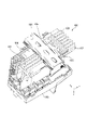
図1は、本実施の形態に係る電子機器用筐体100の外観斜視図である。なお、ここでは、説明のため、電子機器用筐体100の本体部の一部を省略して示している。電子機器用筐体100は、駆動することにより熱を発する発熱部材が、その内部に搭載される。発熱部材は、例えば、PLC(Programmable Logic Controller)やCPU(Central Processing Unit)、SoC(System on a Chip)などの電子機器が挙げられるが、特に限定するものではない。電子機器用筐体100は、レール部材であるDINレール101に接続され、ラック(不図示)などの任意の場所の垂直面に垂直に設置される。
FIG. 1 is an external perspective view of an
電子機器用筐体100は、本体部103と背面部材102とを含んで構成され、内部の機器を搭載するためのハウジング部を構成する。背面部材102は、電子機器用筐体100の背面部を構成する部材である。背面部材102には、DINレール101と接続するための、1または複数の爪部105を備える。図1の例では、2つの爪部105を備える構成を示している。また、背面部材102は、DINレール101を接続するための接続部材104を備える。爪部105と接続部材104とにより、DINレール101と電子機器用筐体100(背面部材102)とを固定して接続する。
The
本実施の形態において、接続部材104は、対向する爪部105側に向けてバネ(不図示)などにより付勢された構造を有し、x軸方向に沿って進退可能として設置される。例えば、DINレール101を背面部材102に取り付ける際には、接続部材104を爪部105から離れる方向(離間方向)に引っ張る(スライドさせる)ことで接続部材104と爪部105との距離を広げる。そして、DINレール101を接続部材104と爪部105の間に配置した後に、接続部材104を放すことで、接続部材104への付勢により接続部材104と爪部105との距離が縮まり、DINレール101が固定される。なお、接続部材104の構成は上記に限定するものではなく、例えば、背面側から(z軸方向に沿って)はめ込み式などにより着脱可能な構成であってもよい。また、爪部105が接続部材104側に向けてバネなどにより付勢された構造であってもよいし、接続部材104と爪部105の両方がバネなどにより互いの方向に向けて付勢された構造であってもよい。
In the present embodiment, the
また、背面部材102は、電子機器用筐体100内部の熱を放熱するためのフィン106、107を備える。図1の例では、DINレール101を挟んで、x軸方向の両側(上下)にフィン106、107が設けられている。なお、フィン106は、7列にて構成され、フィン107は3列にて構成されているが、この構成に限定するものではなく、例えば、SoC112のサイズやSoC112による発熱量などに応じて規定されてよい。また、フィン106、107の形状についても、図1等に示すものに限定するものではなく、例えば、フィン106とフィン107とで異なっていてもよい。
Further, the
図2は、図1にて示した電子機器用筐体100から、DINレール101を外した状態を示す外観斜視図である。
FIG. 2 is an external perspective view showing a state in which the
図3は、電子機器用筐体100のx軸方向における断面を示す概略図である。図3を用いて、電子機器用筐体100の内部の概要を説明する。電子機器用筐体100の内部には、発熱源となる電子機器が備えられる。ここでは、電子機器として、SoC112を例に挙げて説明する。電子機器用筐体100に基板114が設置される。更に基板114上にSoC112が備えられる。図3では、SоC112は、断面が階段状にて示されているが、この構成に限定するものではない。なお、電子機器用筐体100は、基板114を内部に設置するための設置部材を更に備えてもよい。
FIG. 3 is a schematic diagram showing a cross section of the electronic device housing 100 in the x-axis direction. An outline of the inside of the
背面部材102は、電子機器用筐体100の内部に延伸する接触面部110を備え、背面側の部位と一体となるように構成されている。背面部材102(および接触面部110)は、例えば、金属などの高熱伝導の材質により構成される。なお、ここでの「一体」とは、板金一枚構造、鋳造構造、鍛造構造、溶接構造、カシメ構造、圧接構造、または、ネジ連結などいずれの構造により実現されてよい。接触面部110は、y軸方向における一定の厚さを有し、熱伝導性を向上させている。また、接触面部110は、SoC112の表面全体を覆うように構成される。接触面部110とSoC112は、高熱伝導部材111を介して接触するように構成される。高熱伝導部材111は、例えば、高熱伝導の弾性材料により組成され、シート形状などにて構成される。なお、ここでは、接触面部110とSoC112は、高熱伝導部材111を介して間接的に接触した例を示したが、この構成に限定されるものではない。例えば、接触面部110とSoC112が直接的に接触するような構成であってもよい。接触面部110と基板114とは、ネジ部品113により固定され、設置される。ネジ部品113も、背面部材102(および接触面部110)と同様に、高熱伝導の材質により構成されてよい。なお、接触面部110と基板114とを固定するための部品は、ネジ形状に限定するものではなく、例えば、爪形状の部材やバネなどを用いてもよい。
The
(背面部材)
図4は、背面部材102のみの外観斜視図である。背面部材102に一体となって備えられる接触面部110は、ネジ部品113を設置するための1または複数の穴部120を備える。ここでは、2つの穴部120を示しているが、穴部120の数は特に限定するものではなく、電子機器用筐体100のサイズ等に応じて設けられてよい。また、接触面部110は、SoC112の表面と直交する方向の厚みが所定値よりも大きくなるように構成されてよい。ここでの厚みは、接触面部110の熱伝導を向上させるために設計され、例えば、SoC112のサイズやSoC112による発熱量などに応じて規定されてよい。また、接触面部110は、体積が所定値よりも大きくなるように構成されてよい。ここでの体積は、接触面部110の熱伝導を向上させるために設計され、例えば、SoC112のサイズやSoC112による発熱量などに応じて規定されてよい。
(back member)
FIG. 4 is an external perspective view of only the
[熱伝導の経路]
図5~図7は、本実施の形態に係る電子機器用筐体100における熱伝導を説明するための図であり、それぞれ異なる方向から電子機器用筐体100を示している。各図において、矢印は、熱伝導を示す。上述したように、SoC112の動作に伴い、熱が発生する。図5において、SoC112により発生した熱は、まず、基板114の方向と、高熱伝導部材111と接触面部110の方向に伝導する。本実施の形態では、高熱伝導部材111と接触面部110は、高熱伝導の金属材質などにより構成されているため、熱伝導率が高い。一方、基板114は、一般的に樹脂等で構成されているため、熱伝導率が低い。そのため、高熱伝導部材111と接触面部110側に、より多くの熱が伝導する。接触面部110に伝導した熱は更に、電子機器用筐体100の背面側(DINレール101側)に伝導し、外部へと放出される。このとき、熱は、背面部材102の全体へと伝導され、更には、フィン106、107により放熱される。
[Path of heat conduction]
5 to 7 are diagrams for explaining heat conduction in the
図6や図7に示すように、フィン106、107へ伝わった熱は、周辺の気体を温め、煙突効果によりその温められた気体が上昇して放熱が行われる。図6や図7に示す矢印601は、温められて上昇する気流の向きを示す。また、背面部材102に接続されたDINレール101へと熱が伝導し、DINレール101を介しても放熱が行われる。
As shown in FIGS. 6 and 7, the heat transmitted to the
以上、本実施の形態により、電子機器用筐体内部の熱を効率的に外部へ伝導し、電子機器用筐体内部の温度上昇を抑制することが可能となる。そして、SoCなどの高発熱デバイスの温度上昇を抑制し、許容ジャンクション温度を超えることを抑制することができる。また、電子機器用筐体内部で発生した熱を、直接、高熱伝導部材111や接触面部110を介して外部へ伝導することできるため、電子機器用筐体内部での熱の対流を抑止できる。そのため、電子機器用筐体内部に籠った熱を放出するための通風孔を、例えば、電子機器用筐体の側壁部分などへの形成を抑制することができる。その結果として、例えば、防塵性を向上させたり、筐体自体の強度を向上させたりすることが可能となる。また、電子機器用筐体の背面部分のスペースに無駄なくフィンを設置できるため、より効率的な放熱が可能となり、また、筐体内部への放熱容積を小さくすることが可能となる。
As described above, according to the present embodiment, the heat inside the electronic device housing can be efficiently conducted to the outside, and the temperature rise inside the electronic device housing can be suppressed. Then, it is possible to suppress the temperature rise of a high-heat-generating device such as SoC, and to suppress the junction temperature from exceeding the allowable junction temperature. In addition, since the heat generated inside the electronic device housing can be directly conducted to the outside via the high thermal
<実施の形態2>
[電子機器用筐体の構成概要]
図8、図9を参照して、実施の形態2に係る電子機器用筐体の構成例について説明する。なお、以下の図に示す座標系として、x軸、y軸、z軸からなる三次元座標系を示すが、各図の座標系は対応しているものとして説明する。ここでは、x軸方向を上下方向、y軸方向を左右方向、z軸方向を奥行方向として説明する。また、電子機器用筐体の内部に搭載される部品等は様々なものが挙げられるが、ここでは、本願発明に直接関係のある部分のみを説明し、それ以外の構成については、省略又は簡略化して示す。
<Embodiment 2>
[Outline of configuration of housing for electronic device]
A configuration example of the electronic device housing according to the second embodiment will be described with reference to FIGS. 8 and 9. FIG. Although the coordinate system shown in the following figures is a three-dimensional coordinate system consisting of the x-axis, the y-axis, and the z-axis, the explanation will be made assuming that the coordinate systems in each figure correspond to each other. Here, the x-axis direction is the up-down direction, the y-axis direction is the left-right direction, and the z-axis direction is the depth direction. In addition, there are various components and the like to be mounted inside the housing for electronic equipment, but here, only the parts directly related to the present invention will be explained, and other configurations will be omitted or simplified. shown in a simplified form.
図8は、本実施の形態に係る電子機器用筐体200の外観斜視図である。なお、ここでは、説明のため、電子機器用筐体200の本体部の一部を省略して示している。電子機器用筐体200は、駆動することにより熱を発する発熱部材が、その内部に搭載される。発熱部材は、例えば、PLC(Programmable Logic Controller)やCPU(Central Processing Unit)、SoC(System on a Chip)などの電子機器が挙げられるが、特に限定するものではない。電子機器用筐体200は、レール部材であるDINレール201に接続され、ラック(不図示)などの任意の場所の垂直面に垂直に設置される。
FIG. 8 is an external perspective view of
電子機器用筐体200は、本体部203と背面部材202とを含んで構成され、内部の機器を搭載するためのハウジング部を構成する。背面部材202は、電子機器用筐体200の背面部を構成する部材である。背面部材202には、DINレール201と接続するための、1または複数の爪部205を備える。図8の例では、2つの爪部205を備える構成を示している。また、背面部材202は、DINレール101を接続するための接続部材204を備える。爪部205と接続部材204とにより、DINレール201と電子機器用筐体200(背面部材202)とを固定して接続する。
The
本実施の形態において、接続部材204は、対向する爪部205側に向けてバネ(不図示)などにより付勢された構造を有し、x軸方向に沿って進退可能として設置される。例えば、DINレール201を背面部材202に取り付ける際には、接続部材204を爪部205から離れる方向(離間方向)に引っ張る(スライドさせる)ことで接続部材204と爪部205との距離を広げる。そして、DINレール201を接続部材204と爪部205の間に配置した後に、接続部材204を放すことで、接続部材204への付勢により接続部材204と爪部205との距離が縮まり、DINレール101が固定される。なお、接続部材204の構成は上記に限定するものではなく、例えば、背面側から(z軸方向に沿って)はめ込み式などにより着脱可能な構成であってもよい。また、爪部205が接続部材204側に向けてバネなどにより付勢された構造であってもよいし、接続部材204と爪部205の両方がバネなどにより他方の方向に向けて付勢された構造であってもよい。
In this embodiment, the
また、背面部材202は、電子機器用筐体200内部の熱を放熱するためのフィン209、210を備える。図8の例では、DINレール201を挟んで、x軸方向の両側(上下)にフィン209、210が設けられている。なお、フィン210は、7列にて構成され、フィン209は2列にて構成されている。また、フィン209の間にスリット部が形成され、このスリット部から伝熱部材206が突出して、フィンの一部を構成している。また、フィン209、210の形状についても、図8等に示すものに限定するものではなく、例えば、フィン209とフィン210とで異なっていてもよい。
Further, the
また、フィン209の一部を構成するように、伝熱部材206が設けられる。図9は、図8にて示した電子機器用筐体200から、DINレール201を外した状態を示す外観斜視図である。伝熱部材206は、爪部207と、接触部208とを有する。爪部207は、DINレール201に接触するような爪形状の部位を有する。接触部208は、DINレール201の凹部と接触するためのアーチ形状の部位を有する。伝熱部材206、爪部207、接触部208はいずれも、金属などの高熱伝導の材料から構成されるが、すべてが同じ材質である必要は無い。
Also, a
図10は、電子機器用筐体200のx軸方向における断面を示す図である。図10を用いて、電子機器用筐体200の内部の概要を説明する。電子機器用筐体200の内部には、発熱源となる電子機器が備えられる。ここでは、電子機器として、SoC212を例に挙げて説明する。電子機器用筐体200の基板214上にSoC212が設置される。なお、電子機器用筐体200は、基板214を内部に設置するための設置部材を更に備えてもよい。
FIG. 10 is a diagram showing a cross section of the
伝熱部材206は、電子機器用筐体200の内部に延伸するように設置される。また、伝熱部材206は、SoC212の表面全体を覆うように構成される。伝熱部材206とSoC212は、高熱伝導部材211を介して接触するように構成される。高熱伝導部材211は、例えば、高熱伝導の弾性材料により組成され、シート形状にて構成される。なお、ここでは、伝熱部材206とSoC212は、高熱伝導部材211を介して間接的に接触した例を示したが、この構成に限定されるものではない。例えば、伝熱部材206とSoC212が直接的に接触するような構成であってもよい。伝熱部材206と基板214とは、ネジ部品213により固定され、設置される。ネジ部品213も、伝熱部材206と同様に、高熱伝導の材料により構成されてよい。なお、伝熱部材206と基板214とを固定するための部品は、ネジ形状に限定するものではなく、例えば、爪形状の部材やバネなどを用いてもよい。
The
(伝熱部材)
図11は、本実施形態に係る伝熱部材206の外観斜視図である。伝熱部材206は、SoC212を覆うように構成される接触面部220と、背面部材202の一部を構成するように設けられる背面部221を含んで構成される。図11の例では、接触面部220と背面部221とは垂直となるように連結されている。接触面部220は、フィン部220aを有する。フィン部220aは、図9や図10に示すように、背面部材202に設けられたスリット部から突出することで、フィンの一部を構成する。また、接触面部220は、ネジ部品213を設置するための1または複数の穴部222を備える。ここでは、2つの穴部222を示しているが、穴部222の数は特に限定するものではなく、電子機器用筐体200のサイズ等に応じて設けられてよい。
(Heat transfer member)
FIG. 11 is an external perspective view of the
また、背面部221には、爪部207と接触部208が設けられる。爪部207や接触部208は、DINレール201と接触するように配置され、DINレール201に接触することで、DINレール201への熱の伝導経路となる。爪部207や接触部208は、所定方向に一定の形状変化が可能なように弾性を有するような構成であってよい。
Further, the
[テーパ構造による接触]
図12、図13を参照して、本実施の形態に係る主な特徴部分の説明を行う。図12は、本実施の形態に対する比較例としての従来の構成の例を示す図である。電子機器用筐体1203に、DINレール1201が接続されている状態を示す。DINレール1201は、爪部1202と接続部材1204とにより、電子機器用筐体1203に接続され、設置される。また、本実施の形態の接続部材204と同様、接続部材1204は、対抗する爪部1202に向けて付勢される構成であるものとして説明する。このとき、爪部1202や接続部材1204の筐体側の面は、筐体の背面と平行(または、略平行)になっている。そのため、爪部1202や接続部材1204の主たる力の係る方向は、矢印にて示した方向となる。
[Contact by taper structure]
12 and 13, main characterizing portions according to the present embodiment will be described. FIG. 12 is a diagram showing an example of a conventional configuration as a comparative example for this embodiment. A state in which a
図13は、本実施の形態2に係る構成例を示す図である。図8等に示したように、DINレール201は、爪部205と接続部材204とにより、電子機器用筐体200の背面部材202に固定され、設置される。このとき、DINレール201の凹部の底面201bと、接触部208とは接触するように設置される。更に、爪部205と接続部材204は、断面形状が、テーパ形状となっている。つまり、爪部205と接続部材204の筐体側の面は、筐体の背面に対して、一定の角度(傾斜)となるように形成されている。
FIG. 13 is a diagram showing a configuration example according to the second embodiment. As shown in FIG. 8 and the like, the
本実施の形態に係る爪部205と接続部材204の構成により、図13中の矢印にて示すように、付勢された接続部材204による力の向きが変換される。つまり、背面部材202の方向に対する力として、従来の構成における力に加え、DINレール201の幅方向(x軸方向)の力の一部が背面部材202の方向に変換されて付加されることとなる。その結果、DINレール201は、背面部材202の方向に対しても力が加えられ、図12の構成と比べてより強く電子機器用筐体200に押し付けられることとなる。そのため、背面部材202(特に、伝熱部材206)とDINレール201との間の隙間の発生を抑制し、熱伝導率を向上させることが可能となる。なお、図13の例では、接続部材204は、背面部材202側(図中の右側)と、その反対側(図中の左側)の両側において、傾斜を備えた構成例を示しているが、これに限定するものではない。少なくとも、背面部材202側(図中の右側)に一定の傾斜を備えていればよい。また、傾斜の度合いは特に限定するものではなく、電子機器用筐体200のサイズやDINレール201の構造などに応じて規定されてよい。また、テーパ形状は、爪部205と接続部材204の両方に設けられた構成を示したが、これに限定するものではない。例えば、爪部205と接続部材204のいずれか一方にのみ設けられるような構成であってもよいし、それぞれで傾斜の度合いを異ならせてもよい。
Due to the configuration of the
[熱伝導の経路]
図14、図15は、本実施の形態に係る電子機器用筐体200における熱伝導を説明するための図である。各図において、矢印は、熱伝導を示す。上述したように、SoC212の動作に伴い、熱が発生する。図14において、SoC212により発生した熱は、まず、基板214の方向と、高熱伝導部材211や伝熱部材206の方向に伝導する。本実施の形態では、高熱伝導部材211と伝熱部材206はそれぞれ、高熱伝導の材質により構成されているため、熱伝導率が高い。一方、SoC212が構成される基板等は、一般的に樹脂等で構成されているため、熱導電率が低い。そのため、高熱伝導部材211と伝熱部材206側に、より多くの熱が伝導する。伝熱部材206に伝導した熱は更に、電子機器用筐体200の背面部材202(DINレール201側)に伝導し、外部へと放出される。このとき、熱は、背面部材202の全体へと伝導され、フィン209、210により放熱される。
[Path of heat conduction]
14 and 15 are diagrams for explaining heat conduction in the
図15は、DINレール201周りの熱伝導を示す。図13に示したように、DINレール201は、従来よりも背面部材202に強く接触されるため、熱伝導の効率が向上している。更には、熱伝導性の高い材料で構成された爪部207や接触部208を介してもDINレール201へと熱が伝導する。そして、DINレール201を介して放熱が行われる。
FIG. 15 shows heat conduction around
そして、実施の形態1の図6や図7と同様に、フィン209、210へ伝わった熱は、周辺の気体を温め、煙突効果によりその温められた気体が上昇して放熱が行われる。
6 and 7 of the first embodiment, the heat transmitted to the
なお、伝熱部材206が、爪部207や接触部208を備える構成を示したが、いずれか一方のみを備える構成であってもよい。また、図11の例では接触部208は2つのアーチ形状にて形成され、2カ所にてDINレール201の底面201bに接触するような構成であったが、この構成に限定するものではない。例えば、1つのアーチ形状にて構成されDINレール201の底面201b全体にわたって接触するような構成であってもよい。
Although the configuration in which the
以上、実施の形態2に係る電子機器用筐体200は、駆動により熱を発する電子機器を収容する本体部203、本体部203の背面側に設けられ、接続部材204によりDINレール201に接続される背面部材202とを備え、接続部材204は、DINレール201を接続した際に、DINレール201を背面部材202に押し付けるような形状にて構成される。
As described above, the
これにより、電子機器用筐体内部の熱を効率的にDINレール201へ伝導し、電子機器用筐体内部の温度上昇を抑制することが可能となる。そして、SoCなどの高発熱デバイスの温度上昇を抑制し、許容ジャンクション温度を超えることを抑制することができる。また、電子機器用筐体内部で発生した熱を、直接、高熱伝導部材211や伝熱部材206を介してDINレール201へ効率良く伝導することできるため、電子機器用筐体内部での熱の対流を抑止できる。そのため、電子機器用筐体内部に籠った熱を放出するための通風孔を、例えば、電子機器用筐体の側壁部分などへの形成を抑制することができる。その結果として、例えば、防塵性を向上させたり、筐体自体の強度を向上させたりすることが可能となる。また、電子機器用筐体の背面部分のスペースに無駄なくフィンを設置できるため、より効率的な放熱が可能となり、また、筐体内部への放熱容積を小さくすることが可能となる。
As a result, the heat inside the electronic device housing can be efficiently conducted to the
また、伝熱部材206に設けられる爪部207や接触部208において弾力性を有する構成とすることで、接触力が安定し、冷却効果を安定させることができる。また、接触部208は、DINレール201の底面201bに接触させる構成のため、接触面積を増大させて、伝熱量を増加させ、冷却効果を向上させることができる。
Further, by configuring the
また、接続部材204は、DINレール201と接触する面が、背面部材202の背面に対して傾斜を有するテーパ形状にて構成される。
Also, the
これにより、DINレールを背面部材の背面に対する接触を強めることができ、より効率的に熱を伝導させることが可能となる。 This allows the DIN rail to make stronger contact with the back surface of the back member, allowing more efficient heat conduction.
また、背面部材202は、DINレール201を挟んで、接続部材204と対向するように配置された、DINレール部材を接続するための爪部205を有し、爪部205は、DINレール201と接触する面が、背面部材202の背面に対して傾斜を有するテーパ形状にて構成される。
In addition, the
これにより、DINレールを背面部材の背面に対する接触面積を増加させることができ、より効率的に熱を伝導させることが可能となる。 As a result, the contact area of the DIN rail with the back surface of the back member can be increased, and heat can be conducted more efficiently.
また、接続部材204または爪部205の少なくとも一方は、他方への方向に沿って進退可能であり、かつ、他方側に向けて付勢されている。
At least one of the
これにより、DINレールを取付けた際には、接続部材204と爪部205の少なくとも一方に対して行われている付勢の力が、DINレールを背面方向へ押し付ける側への力へと変換される。そのため、より強い力にて確実にDINレールを背面部材に接触させることができ、その接触により冷却効果を安定させることが可能となる。
As a result, when the DIN rail is attached, the biasing force applied to at least one of the
また、SoC212などの電子機器の表面と対向して直接的または間接的に接触するように、本体部203の内部に延伸して配置された伝熱部材206を更に有し、伝熱部材206は、電子機器を設置するための部材よりも高熱伝導率の材料により構成され、かつ、DINレール201に接触するように構成される。
これにより、電子機器用筐体内部の熱を効率的にDINレール201へ伝導し、電子機器用筐体内部の温度上昇を抑制することが可能となる。
Further, a
As a result, the heat inside the electronic device housing can be efficiently conducted to the
また、伝熱部材206は、DINレール201と接触する爪部207を備える。
Also, the
これにより、電子機器用筐体は、電子機器により発する熱を効率的にDINレールに伝導することが可能となる。 This allows the electronic device enclosure to efficiently conduct heat generated by the electronic device to the DIN rail.
また、伝熱部材206は、DINレール201の凹部の底面と接触する接触部208を備える。
The
これにより、電子機器用筐体は、電子機器により発する熱を効率的にDINレールに伝導することが可能となる。 This allows the electronic device enclosure to efficiently conduct heat generated by the electronic device to the DIN rail.
また、伝熱部材206は、電子機器の表面全体を覆うように構成される。
Also, the
これにより、電子機器用筐体は、電子機器により発する熱を効率的に伝熱部材206に伝導することが可能となる。
As a result, the electronic device housing can efficiently conduct heat generated by the electronic device to the
また、伝熱部材206の一部が、背面部材202に設けられるフィンの一部を構成する。
A portion of the
これにより、電子機器用筐体は、電子機器により発する熱を効率的に外部に伝導することが可能となる。 As a result, the electronic device housing can efficiently conduct heat generated by the electronic device to the outside.
<その他の実施形態>
実施の形態2において、伝熱部材206が、高熱伝導率を有する材料により構成される爪部207や接触部208を備えている構成を示した。このような爪部や接続部は、実施の形態1にて示した背面部材102が備えるような構成であってもよい。このような構成により、高熱伝導率を有する材料により構成される背面部材102から更に、熱伝導性の高い材料で構成された爪部や接触部を介してもDINレールへと効率よく熱を伝導させることが可能となる。この場合、爪部や接触部と、背面部材102は、いずれも高熱伝導率の材料により構成されるが、同じ材料である必要はない。
<Other embodiments>
In the second embodiment, the
実施の形態2において、伝熱部材206は、高熱伝導率を有する材料により構成される構成を示した。更に、背面部材202が高熱伝導率を有する材料により構成されるような構成であってもよい。このような構成により、高熱伝導率の材料により構成される背面部材202から更に、フィン209、210を介して効率的に放熱を行うことが可能となる。この場合、伝熱部材206と、背面部材202は、いずれも高熱伝導率の材料により構成されるが、同じ材料である必要はない。
In the second embodiment, the
以上、図面を参照しながら各種の実施形態について説明したが、本開示は係る例に限定されないことは言うまでもない。当業者であれば、特許請求の範囲に記載された範疇内において、各種の変更例、修正例、置換例、付加例、削除例、均等例に相当し得ることは明らかであり、それらについても当然に本開示の技術的範囲に属するものと了解される。また、発明の趣旨を逸脱しない範囲において、上述した各種の実施形態における各構成要素を任意に組み合わせてもよい。 Various embodiments have been described above with reference to the drawings, but it goes without saying that the present disclosure is not limited to such examples. It is clear that a person skilled in the art can correspond to various modifications, modifications, substitutions, additions, deletions, and equivalents within the scope of the claims. Naturally, it is understood that it belongs to the technical scope of the present disclosure. In addition, the constituent elements of the various embodiments described above may be arbitrarily combined without departing from the gist of the invention.
本開示は、電子機器用筐体内部にて発生した熱を効率よく外部へ伝導し、電子機器用筐体内部の温度上昇を抑制することが可能な電子機器用筐体として有用である。 INDUSTRIAL APPLICABILITY The present disclosure is useful as an electronic device housing capable of efficiently conducting heat generated inside the electronic device housing to the outside and suppressing temperature rise inside the electronic device housing.
100,200 電子機器用筐体
101,201 DINレール
102,202 背面部材
103,203 本体部
104,204 接続部材
105,205 爪部
106,107,209,210 フィン
111,211 高熱伝導部材
112,212 SoC
113,213 ネジ部品
114,214 基板
120 穴部
201a 座面
201b 底面
206 伝熱部材
207 爪部
208 接触部
220 接触面部
220a フィン部
221 背面部
222 穴部
100, 200
113, 213
Claims (9)
前記本体部の背面側に設けられ、接続部材によりレール部材に接続される背面部材と
を備え、
前記接続部材は、前記レール部材を接続した際に、前記レール部材を前記背面部材に押し付けるような形状にて構成される、
電子機器用筐体。 a main body that houses an electronic device that generates heat when driven;
a back member provided on the back side of the main body and connected to the rail member by a connection member;
The connection member is configured to have a shape that presses the rail member against the back member when the rail member is connected,
Enclosure for electronics.
請求項1に記載の電子機器用筐体。 A surface of the connection member that contacts the rail member has a tapered shape that is inclined with respect to the back surface of the back surface member.
The housing for electronic equipment according to claim 1 .
前記爪部は、前記レール部材と接触する面が、前記背面部材の背面に対して傾斜を有するテーパ形状にて構成される、
請求項1または2に記載の電子機器用筐体。 The back member has a claw portion for connecting the rail member arranged to face the connection member with the rail member interposed therebetween,
The claw portion has a tapered shape in which a surface that contacts the rail member is inclined with respect to the back surface of the back surface member,
The housing for electronic equipment according to claim 1 or 2.
請求項3に記載の電子機器用筐体。 At least one of the connecting member and the claw is movable forward and backward along the other direction and is biased toward the other side,
The housing for electronic equipment according to claim 3 .
前記伝熱部材は、
前記電子機器を設置するための部材よりも高熱伝導率の材料により構成され、かつ、
前記レール部材に接触するように構成される、
請求項1~4のいずれか一項に記載の電子機器用筐体。 further comprising a heat transfer member extending inside the main body so as to directly or indirectly contact the surface of the electronic device;
The heat transfer member is
made of a material with a higher thermal conductivity than the member for installing the electronic device, and
configured to contact the rail member;
The housing for electronic equipment according to any one of claims 1 to 4.
請求項5に記載の電子機器用筐体。 The heat transfer member includes a claw portion that contacts the rail member,
The housing for electronic equipment according to claim 5 .
請求項5または6に記載の電子機器用筐体。 The heat transfer member includes a contact portion that contacts the bottom surface of the recess of the rail member,
7. The housing for electronic equipment according to claim 5 or 6.
請求項5~7のいずれか一項に記載の電子機器用筐体。 The heat transfer member is configured to cover the entire surface of the electronic device,
The housing for electronic equipment according to any one of claims 5 to 7.
請求項5~8のいずれか一項に記載の電子機器用筐体。 A part of the heat transfer member constitutes a part of the fins provided on the back member,
The housing for electronic equipment according to any one of claims 5 to 8.
Priority Applications (2)
| Application Number | Priority Date | Filing Date | Title |
|---|---|---|---|
| JP2021048761A JP2022147499A (en) | 2021-03-23 | 2021-03-23 | Enclosure for electronic equipment |
| PCT/JP2021/048724 WO2022201723A1 (en) | 2021-03-23 | 2021-12-27 | Housing for electronic apparatus |
Applications Claiming Priority (1)
| Application Number | Priority Date | Filing Date | Title |
|---|---|---|---|
| JP2021048761A JP2022147499A (en) | 2021-03-23 | 2021-03-23 | Enclosure for electronic equipment |
Publications (2)
| Publication Number | Publication Date |
|---|---|
| JP2022147499A true JP2022147499A (en) | 2022-10-06 |
| JP2022147499A5 JP2022147499A5 (en) | 2024-03-22 |
Family
ID=83396744
Family Applications (1)
| Application Number | Title | Priority Date | Filing Date |
|---|---|---|---|
| JP2021048761A Pending JP2022147499A (en) | 2021-03-23 | 2021-03-23 | Enclosure for electronic equipment |
Country Status (2)
| Country | Link |
|---|---|
| JP (1) | JP2022147499A (en) |
| WO (1) | WO2022201723A1 (en) |
Family Cites Families (8)
| Publication number | Priority date | Publication date | Assignee | Title |
|---|---|---|---|---|
| JPS6030587U (en) * | 1983-08-09 | 1985-03-01 | 和泉電気株式会社 | Electrical equipment mounting equipment |
| JPH062311Y2 (en) * | 1988-03-14 | 1994-01-19 | 富士電機株式会社 | Contactless switch cooling body |
| JP2561688Y2 (en) * | 1992-09-28 | 1998-02-04 | 横河電機株式会社 | Rail mounting device for electronic equipment |
| JP3744994B2 (en) * | 1995-12-08 | 2006-02-15 | 株式会社キーエンス | Detector amplifier unit |
| JP4063382B2 (en) * | 1998-02-05 | 2008-03-19 | オムロン株式会社 | Electrical equipment |
| JP2006253531A (en) * | 2005-03-14 | 2006-09-21 | Cosel Co Ltd | Electrical component mounting arrangement |
| US11178791B2 (en) * | 2013-12-30 | 2021-11-16 | Schneider Electric USA, Inc. | Apparatus for increasing heat dissipation capacity of a DIN rail mounted enclosure |
| US11991868B2 (en) * | 2018-03-05 | 2024-05-21 | Sew-Eurodrive Gmbh & Co. Kg | Electrical appliance arrangement having an electrical appliance which can be fastened to a support element, in particular a wall |
-
2021
- 2021-03-23 JP JP2021048761A patent/JP2022147499A/en active Pending
- 2021-12-27 WO PCT/JP2021/048724 patent/WO2022201723A1/en active Application Filing
Also Published As
| Publication number | Publication date |
|---|---|
| WO2022201723A1 (en) | 2022-09-29 |
Similar Documents
| Publication | Publication Date | Title |
|---|---|---|
| JP5082970B2 (en) | Circuit board equipment | |
| JP6655824B2 (en) | Imaging device | |
| JP4387314B2 (en) | Electrical junction box | |
| WO2011096218A1 (en) | Heat radiation device and electronic equipment using the same | |
| US7468890B2 (en) | Graphics card heat-dissipating device | |
| JP2012023329A (en) | Substrate unit and electronic device | |
| TWI722195B (en) | Electronic device and heat radiation structure of electronic device | |
| JP2006278941A (en) | Heat sink device and plug-in unit | |
| TW201334679A (en) | Heat dissipating module | |
| JP6500450B2 (en) | Heat dissipation method and heat dissipation device | |
| WO2022201715A1 (en) | Electronic device housing | |
| JP2010103370A (en) | Electronic control device | |
| JP6619491B2 (en) | Electronics | |
| WO2022201723A1 (en) | Housing for electronic apparatus | |
| JP6892756B2 (en) | Heat dissipation structure | |
| TWI424140B (en) | Flattened heat dissipation structure with fins parallel to heat receiving surface | |
| CN115397192A (en) | Heat radiator | |
| JP2018096613A (en) | Heat radiation structure and electronic apparatus | |
| JP2016131218A (en) | Heat radiation device | |
| JP2015216143A (en) | Heat radiation structure of heating element | |
| JP2016219641A (en) | Heat sink and housing for base station | |
| JP3711032B2 (en) | Cooling structure for heat-generating electronic components | |
| WO2024058186A1 (en) | Electrical junction box | |
| KR102642224B1 (en) | Heat sink and electronics unit | |
| TWI537567B (en) | Electronic load testing device |
Legal Events
| Date | Code | Title | Description |
|---|---|---|---|
| A621 | Written request for application examination |
Free format text: JAPANESE INTERMEDIATE CODE: A621 Effective date: 20240125 |
|
| A521 | Request for written amendment filed |
Free format text: JAPANESE INTERMEDIATE CODE: A523 Effective date: 20240313 |