JP6655824B2 - Imaging device - Google Patents
Imaging device Download PDFInfo
- Publication number
- JP6655824B2 JP6655824B2 JP2017008695A JP2017008695A JP6655824B2 JP 6655824 B2 JP6655824 B2 JP 6655824B2 JP 2017008695 A JP2017008695 A JP 2017008695A JP 2017008695 A JP2017008695 A JP 2017008695A JP 6655824 B2 JP6655824 B2 JP 6655824B2
- Authority
- JP
- Japan
- Prior art keywords
- imaging device
- heat sink
- substrate
- heat
- fins
- Prior art date
- Legal status (The legal status is an assumption and is not a legal conclusion. Google has not performed a legal analysis and makes no representation as to the accuracy of the status listed.)
- Active
Links
- 238000003384 imaging method Methods 0.000 title claims description 85
- 239000000758 substrate Substances 0.000 claims description 112
- 230000002093 peripheral effect Effects 0.000 claims description 25
- 230000005855 radiation Effects 0.000 claims description 19
- 230000017525 heat dissipation Effects 0.000 claims description 15
- 238000005286 illumination Methods 0.000 claims description 15
- 230000001678 irradiating effect Effects 0.000 claims description 4
- 230000005484 gravity Effects 0.000 claims description 3
- 238000003780 insertion Methods 0.000 description 22
- 230000037431 insertion Effects 0.000 description 22
- 230000000149 penetrating effect Effects 0.000 description 6
- 210000000078 claw Anatomy 0.000 description 5
- 238000012986 modification Methods 0.000 description 4
- 230000004048 modification Effects 0.000 description 4
- 229910052782 aluminium Inorganic materials 0.000 description 3
- XAGFODPZIPBFFR-UHFFFAOYSA-N aluminium Chemical compound [Al] XAGFODPZIPBFFR-UHFFFAOYSA-N 0.000 description 3
- 230000012447 hatching Effects 0.000 description 3
- 238000012544 monitoring process Methods 0.000 description 3
- 239000010409 thin film Substances 0.000 description 3
- 238000010586 diagram Methods 0.000 description 2
- 238000009413 insulation Methods 0.000 description 2
- 239000004925 Acrylic resin Substances 0.000 description 1
- 229920000178 Acrylic resin Polymers 0.000 description 1
- RYGMFSIKBFXOCR-UHFFFAOYSA-N Copper Chemical compound [Cu] RYGMFSIKBFXOCR-UHFFFAOYSA-N 0.000 description 1
- 230000004308 accommodation Effects 0.000 description 1
- 230000005540 biological transmission Effects 0.000 description 1
- 239000011889 copper foil Substances 0.000 description 1
- 238000004512 die casting Methods 0.000 description 1
- 230000000694 effects Effects 0.000 description 1
- 239000004519 grease Substances 0.000 description 1
- 230000001771 impaired effect Effects 0.000 description 1
- 239000000463 material Substances 0.000 description 1
- 239000007769 metal material Substances 0.000 description 1
- 230000000191 radiation effect Effects 0.000 description 1
- 239000011347 resin Substances 0.000 description 1
- 229920005989 resin Polymers 0.000 description 1
Images


Classifications
-
- G—PHYSICS
- G03—PHOTOGRAPHY; CINEMATOGRAPHY; ANALOGOUS TECHNIQUES USING WAVES OTHER THAN OPTICAL WAVES; ELECTROGRAPHY; HOLOGRAPHY
- G03B—APPARATUS OR ARRANGEMENTS FOR TAKING PHOTOGRAPHS OR FOR PROJECTING OR VIEWING THEM; APPARATUS OR ARRANGEMENTS EMPLOYING ANALOGOUS TECHNIQUES USING WAVES OTHER THAN OPTICAL WAVES; ACCESSORIES THEREFOR
- G03B21/00—Projectors or projection-type viewers; Accessories therefor
- G03B21/14—Details
- G03B21/16—Cooling; Preventing overheating
-
- F—MECHANICAL ENGINEERING; LIGHTING; HEATING; WEAPONS; BLASTING
- F21—LIGHTING
- F21V—FUNCTIONAL FEATURES OR DETAILS OF LIGHTING DEVICES OR SYSTEMS THEREOF; STRUCTURAL COMBINATIONS OF LIGHTING DEVICES WITH OTHER ARTICLES, NOT OTHERWISE PROVIDED FOR
- F21V29/00—Protecting lighting devices from thermal damage; Cooling or heating arrangements specially adapted for lighting devices or systems
- F21V29/50—Cooling arrangements
- F21V29/70—Cooling arrangements characterised by passive heat-dissipating elements, e.g. heat-sinks
- F21V29/74—Cooling arrangements characterised by passive heat-dissipating elements, e.g. heat-sinks with fins or blades
- F21V29/76—Cooling arrangements characterised by passive heat-dissipating elements, e.g. heat-sinks with fins or blades with essentially identical parallel planar fins or blades, e.g. with comb-like cross-section
-
- B—PERFORMING OPERATIONS; TRANSPORTING
- B60—VEHICLES IN GENERAL
- B60Q—ARRANGEMENT OF SIGNALLING OR LIGHTING DEVICES, THE MOUNTING OR SUPPORTING THEREOF OR CIRCUITS THEREFOR, FOR VEHICLES IN GENERAL
- B60Q3/00—Arrangement of lighting devices for vehicle interiors; Lighting devices specially adapted for vehicle interiors
- B60Q3/20—Arrangement of lighting devices for vehicle interiors; Lighting devices specially adapted for vehicle interiors for lighting specific fittings of passenger or driving compartments; mounted on specific fittings of passenger or driving compartments
- B60Q3/233—Seats; Arm rests; Head rests
-
- B—PERFORMING OPERATIONS; TRANSPORTING
- B60—VEHICLES IN GENERAL
- B60R—VEHICLES, VEHICLE FITTINGS, OR VEHICLE PARTS, NOT OTHERWISE PROVIDED FOR
- B60R11/00—Arrangements for holding or mounting articles, not otherwise provided for
- B60R11/04—Mounting of cameras operative during drive; Arrangement of controls thereof relative to the vehicle
-
- F—MECHANICAL ENGINEERING; LIGHTING; HEATING; WEAPONS; BLASTING
- F21—LIGHTING
- F21V—FUNCTIONAL FEATURES OR DETAILS OF LIGHTING DEVICES OR SYSTEMS THEREOF; STRUCTURAL COMBINATIONS OF LIGHTING DEVICES WITH OTHER ARTICLES, NOT OTHERWISE PROVIDED FOR
- F21V29/00—Protecting lighting devices from thermal damage; Cooling or heating arrangements specially adapted for lighting devices or systems
- F21V29/50—Cooling arrangements
- F21V29/502—Cooling arrangements characterised by the adaptation for cooling of specific components
- F21V29/503—Cooling arrangements characterised by the adaptation for cooling of specific components of light sources
-
- H—ELECTRICITY
- H01—ELECTRIC ELEMENTS
- H01L—SEMICONDUCTOR DEVICES NOT COVERED BY CLASS H10
- H01L23/00—Details of semiconductor or other solid state devices
- H01L23/34—Arrangements for cooling, heating, ventilating or temperature compensation ; Temperature sensing arrangements
- H01L23/36—Selection of materials, or shaping, to facilitate cooling or heating, e.g. heatsinks
- H01L23/367—Cooling facilitated by shape of device
-
- H—ELECTRICITY
- H04—ELECTRIC COMMUNICATION TECHNIQUE
- H04N—PICTORIAL COMMUNICATION, e.g. TELEVISION
- H04N23/00—Cameras or camera modules comprising electronic image sensors; Control thereof
-
- H—ELECTRICITY
- H05—ELECTRIC TECHNIQUES NOT OTHERWISE PROVIDED FOR
- H05K—PRINTED CIRCUITS; CASINGS OR CONSTRUCTIONAL DETAILS OF ELECTRIC APPARATUS; MANUFACTURE OF ASSEMBLAGES OF ELECTRICAL COMPONENTS
- H05K7/00—Constructional details common to different types of electric apparatus
- H05K7/20—Modifications to facilitate cooling, ventilating, or heating
Description
本発明は、撮像装置に関し、特に、車両のシートに着座した乗員の状態を監視するための撮像装置に関するものである。 The present invention relates to an imaging device, and more particularly to an imaging device for monitoring a state of an occupant seated on a vehicle seat.
従来から、この種の撮像装置として、例えば特許文献1に示されるものが知られている。この特許文献1には、表面に配線が形成された基板と、この基板の表面における左右方向中央の位置で基板の表面側に実装されかつ基板と電気的に接続された撮像部と、撮像部に対し左右側方に所定の間隔をあけた位置で基板の表面側に実装されかつ基板と電気的に接続された左右一対のLED素子とを備えた撮像装置が開示されている。
2. Description of the Related Art Conventionally, as an imaging apparatus of this type, for example, an imaging apparatus disclosed in
また、特許文献2には、車両のウィンドシールドに表示像を投影するヘッドアップディスプレイ装置が開示されている。このヘッドアップディスプレイ装置は、表面に配線が形成された基板と、基板の表面側に実装されかつ基板と電気的に接続された一対のLED素子と、前面が基板の裏面に当接した状態で取付固定されたヒートシンクとを備えている。このヒートシンクは、基板の発熱を放散するためのものであり、前面が平坦面状に形成されたベース部と、ベース部の後面に互いに間隔をあけた状態で一体に突設された複数のフィンと、を有している。
上記特許文献1の撮像装置において、LED素子は撮像部の撮影領域に対し照明光を照射するためのものである。そして、LED素子から照明光が照射されているときに、LED素子の消費電力に起因してLED素子が発熱し、その熱がLED素子の実装側となる基板表面に伝わることになる。しかしながら、特許文献1の撮像装置では、特許文献2に開示されたヒートシンクが設けられていないため、LED素子に起因する基板の発熱を適切に放熱することができなかった。
In the imaging device of
また、仮に特許文献1の撮像装置に対し上記ヒートシンクを適用した場合、特許文献2のように、LED素子が実装されていない基板の裏面側にヒートシンクのベース部前面を当接させた状態で取付固定することになる。しかしながら、このような構造では、基板表面の発熱を、一般的に熱伝導率が低い樹脂材からなる基板を介して基板裏面側に配設されたヒートシンクのフィンに伝熱させなければならない。すなわち、特許文献1の撮像装置に対し上記ヒートシンクを適用した構造であっても、LED素子に起因する基板の発熱を効率よく放熱することができず、その結果、基板が高温状態となった場合に撮像装置としての動作環境を十分に維持することできないという問題があった。
Also, if the above-described heat sink is applied to the imaging device of
本発明は斯かる点に鑑みてなされたものであり、その目的は、発光素子に起因する基板の発熱を効率よく放熱し、高温状態となっても信頼性が高い動作環境を得ることにある。 The present invention has been made in view of the above, and an object of the present invention is to efficiently radiate heat generated from a substrate due to a light emitting element and obtain a highly reliable operating environment even in a high temperature state. .
上記の目的を達成するために、本発明の一実施形態に係る撮像装置は、撮像部と、表面
に所定の配線パターンが形成された基板と、基板の表面に、配線パターンと電気的に接続された状態で実装され、撮像部の撮像方向に向かって照明光を照射するための発光素子と、基板の、発光素子の実装面側に配置され、基板の発熱を放散するヒートシンクと、を備えている。そして、ヒートシンクは、伝熱面が基板の表面に対向するように伝熱可能に取り付けられかつ発光素子の照明光を透過可能なベース部と、放熱面に互いに間隔をあけた状態で一体に突設され、空気により冷却される複数のフィンとを有していることを特徴とする。さらに、ヒートシンクの放熱面には、発光素子の照明光を透過可能なカバー部材が複数のフィンを覆うように設けられており、カバー部材は、ヒートシンクの放熱面側に複数のフィンと間隔をあけた位置に配置された前面部と、前面部の周縁から後方に延びる周壁部と、を有し、カバー部材の周壁部には、ヒートシンクとカバー部材との間の空間を外部に連通する複数の開口部が互いに間隔をあけて開口されている。
In order to achieve the above object, an imaging device according to an embodiment of the present invention includes an imaging unit, a substrate having a predetermined wiring pattern formed on a surface thereof, and a wiring pattern electrically connected to a surface of the substrate. A light-emitting element for irradiating illumination light in the imaging direction of the imaging unit, and a heat sink disposed on the mounting surface side of the light-emitting element of the substrate and dissipating heat of the substrate. ing. The heat sink is mounted so as to be able to conduct heat so that the heat transfer surface faces the surface of the substrate, and projects integrally with the base portion capable of transmitting the illumination light of the light emitting element with the heat dissipation surface spaced apart from each other. And a plurality of fins that are provided and cooled by air. Further, a cover member capable of transmitting the illumination light of the light emitting element is provided on the heat radiation surface of the heat sink so as to cover the plurality of fins, and the cover member is spaced apart from the plurality of fins on the heat radiation surface side of the heat sink. And a peripheral wall portion extending rearward from the peripheral edge of the front portion, and a plurality of peripheral walls of the cover member that communicate a space between the heat sink and the cover member to the outside. The openings are spaced apart from each other.
本発明によると、ヒートシンクは、発光素子に起因する基板の表面の発熱を、基板を介することなく、ベース部の伝熱面からベース部の放熱面に設けられた複数のフィンに伝熱させて放散することが可能となる。したがって、本発明では、発光素子に起因する基板の発熱を効率よく放熱することができ、高温状態となっても信頼性が高い動作環境を得ることができる。 According to the present invention, the heat sink transfers heat generated on the surface of the substrate due to the light emitting element from the heat transfer surface of the base portion to the plurality of fins provided on the heat dissipation surface of the base portion without passing through the substrate. It is possible to dissipate. Therefore, according to the present invention, heat generated from the substrate due to the light emitting element can be efficiently radiated, and a highly reliable operating environment can be obtained even in a high temperature state.
以下、本発明の実施形態を図面に基づいて詳細に説明する。以下の実施形態の説明は、本質的に例示に過ぎず、本発明、その適用物或いはその用途を制限することを意図するものではない。 Hereinafter, embodiments of the present invention will be described in detail with reference to the drawings. The description of the embodiments below is merely an example in nature, and is not intended to limit the present invention, its applications, and its uses.
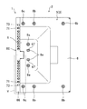
図1〜図4は、本発明の実施形態に係る撮像装置1の全体を示している。撮像装置1は、車両に搭載され、車両のシートに着座した乗員の状態を監視するための装置であり、例えば自動車内のステアリングコラム上に設置される。
1 to 4 show the entirety of an
ここで、以下の説明では、後述するLED用基板20の表面20a側を前側(前方)とし、LED用基板20の裏面20b側を後側(後方)として撮像装置1の前後方向の位置関係を表すものとする。なお、このような位置関係は、撮像装置1が車両(自動車)内に設置される際の実際の前後方向とは無関係である。
Here, in the following description, the front-back (front) is the front surface 20a side of the
(撮像部)
撮像装置1は、車両のシートに着座した乗員の状態を監視するための撮像部2を備えている。撮像部2は、筐体部3、メイン基板10、カメラユニット11を主たる要素部材として有している。
(Imaging unit)
The
図1〜図4に示すように、上記筐体部3は、例えばアルミニウムなどの金属材からなり、撮像装置1のケーシングを構成している。具体的に、図5に示すように、筐体部3は、底板部4および上蓋部5を有している。また、筐体部3には、底板部4が上蓋部5に取付固定された状態で前側全体が開口する前側開口部が形成されている。
As shown in FIGS. 1 to 4, the
底板部4は、平面視で略矩形板状に形成されている。底板部4の各隅角部には、ビスV,V,…を挿入するためのビス挿入孔4a,4a,…が形成されている。また、底板部4の前部には、左右方向略中央の位置に後述するカバー部材60の爪部67,67に係合する係合孔4b,4bが形成されている。
The
上蓋部5は、平面視で略矩形状の天板部6と、天板部6の左右両側部および後部の各周縁から下方に延びる側壁部7,7,…とを有している。天板部6の左右両側部に対応する各側壁部7において、その前部および後部には、底板部4のビス挿入部4a,4aに挿入されたビスV,Vを締結するためのビス締結部7a,7a(図5では1つのみ図示)が形成されている。また、天板部6の前部には、左右方向略中央の位置に後述するカバー部材60の爪部67,67に係合する係合孔6a,6aが形成されている。さらに、天板部6の左右両側部に対応する各側壁部7の前部にも上記天板部6の係合孔6aと同様に、カバー部材60の爪部67に係合する係合孔7bが形成されている。
The
天板部6の左右両側部には、メイン基板10をビスV,V,…で天板部6に締結固定するためのビス締結部6b,6b,…が形成されている。また、天板部6前側の左右両側部には、後述するヒートシンク50をビスV,Vで天板部6に締結固定するためのビス締結部6c,6cが形成されている。
天板部6の前部には、筐体部3内にカメラユニット11を収容するためのカメラ収容部8が設けられている。このカメラ収容部8は、天板部6前側の左右方向略中央が天板部6から上方に向かって略台形状に突出するように形成されている。また、カメラ収容部8の頂部には、カメラユニット11をビスV,Vでカメラ収容部8に締結固定するためのビス締結部8a,8aが形成されている。
At the front of the
上記メイン基板10は、カメラユニット11および後述するLEDユニット19のそれぞれと電気的に接続されている。図5に示すように、メイン基板10は、平面視で略矩形状に形成されていて、その各隅角部には天板部6に取付固定するためのビス挿入孔10a,10a,…が上下方向に向かって貫通形成されている。メイン基板10は、その下側からビス挿入孔10a,10a,…に挿入されたビスV,V,…が天板部6のビス締結部6b,6b,…に締結された状態で上蓋部5に取り付けられている。
The
図5に示すように、上記カメラユニット11は、ユニット本体部12を有している。ユニット本体部12は、例えばアルミダイカストからなる。ユニット本体部12の左右両端には、カメラユニット11を上蓋部5のカメラ収容部8に取り付けるための取付部13,13が配設されている。この各取付部13には、ビスVを挿入するためのビス挿入孔13aが上下方向に向かって貫通形成されている。カメラユニット11は、ユニット本体部12の下側からビス挿入孔13a,13aに挿入されたビスV,Vがカメラ収容部8のビス締結部8a,8aに締結された状態で上蓋部5のカメラ収容部8に取り付けられている。
As shown in FIG. 5, the
ユニット本体部12の左右方向中央には、円筒状のレンズ部14が設けられている。レンズ部14は、先端に配設されたレンズ面14aが後述するカバー部材60のレンズ用貫通孔62と対向するように配置されている。また、ユニット本体部12の後側には、カメラ用基板15が配設されている。このカメラ用基板15は、フラットケーブル16を介してメイン基板10に電気的に接続されている。
A
(LEDユニット)
次に、図5に示すように、撮像装置1は、撮像部2のカメラユニット11による撮像領域に対して照明光を照射するためのLEDユニット19を備えている。図6および図7に示すように、LEDユニット19は、LED用基板20(基板)、LED素子30(発光素子)、放熱シート40、ヒートシンク50を主たる要素部材として有している。
(LED unit)
Next, as shown in FIG. 5, the
上記LED用基板20は、その表面20aが撮像装置1の前方に向かうように筐体部3内に配置されている。LED用基板20は、左右の上側隅角部がそれぞれ面取りされていて、正面視でその外径が筐体部3の前側開口部内に納まるように形成されている。
The
LED用基板20の左右方向中央には、上端部から略円弧状に凹陥した切り欠き凹部21が形成されている。この切り欠き凹部21は、上蓋部5のカメラ収容部8に取付固定されたカメラユニット11のレンズ部14下側を外嵌合状態で保持可能となっている。
At the center of the
LED用基板20には、前後方向に向かって貫通した複数のビス挿入孔20c,20c,…が所定の位置に形成されている。また、LED用基板20の下側には、前後方向に向かって貫通した位置決め孔20d,20dが左右方向に間隔をあけて形成されている。この位置決め孔20d,20dは、後述するヒートシンク50の位置決め用突起51d,51dの位置に対応するように配置されている。
A plurality of
図8に示すように、LED用基板20の表面20aには、銅箔からなる所定の配線パターン22が形成されている。具体的に、この配線パターン22は、LED用基板20の表面20aに沿って面状に広がるように形成されたアノードおよびカソードの面状パターン22a,22b,…を有している。アノードの面状パターン22a,22aは、切り欠き凹部21の左右側方の位置にそれぞれ配置されている。カソードの面状パターン22b,22bは、LED用基板20の左右両端側でアノードの各面状パターン22aに隣り合う位置にそれぞれ配置されている。
As shown in FIG. 8, a
図9に示すように、LED用基板20の裏面20bにも、所定の配線パターン23が形成されている。具体的に、この配線パターン23は、LED用基板20の裏面20bに沿って面状に広がるように形成されたアノードおよびカソードの面状パターン23a,23b,…を有している。アノードの面状パターン23a,23aは、切り欠き凹部21の左右側方の位置にそれぞれ配置されている。カソードの面状パターン23b,23bは、LED用基板20の左右両端側でアノードの各面状パターン23aに隣り合う位置にそれぞれ配置されている。
As shown in FIG. 9, a
図8および図9に示すように、LED用基板20には、表面20a側の配線パターン22と裏面20b側の配線パターン23とが互いに連通するように前後方向に貫通するスルーホール24,24,…が形成されている。アノードの面状パターン22a,23aの各々は、スルーホール24,24,…により互いに電気的に接続されている。同様に、カソードの面状パターン22b,23bの各々についても、スルーホール24,24,…により互いに電気的に接続されている。
As shown in FIGS. 8 and 9, through
LED用基板20の表面20aには、グランドの面状パターン22cが形成されている。また、LED用基板20の裏面20bにも、グランドの面状パターン23c,23cが形成されている。グランドの面状パターン22c,23cの各々は、ビス挿入孔20c,20c,…が配置された位置を含むように面状に形成されている。
On the surface 20a of the
なお、図6では、面状パターン22a,22b,22cおよびスルーホール24,24,…の図示を省略している。図7についても、図6と同様に、面状パターン23a,23b,23cおよびスルーホール24,24,…の図示を省略している。また、図8では、面状パターン22a,22b,22cの各々を強調して示すためにドットハッチングで表している。図9についても、図8と同様に、面状パターン23a,23b,23cの各々をドットハッチングで表している。
6, the illustration of the
図6および図7に示すように、上記LED素子30は、撮像装置1の前側、すなわち撮像部2の撮像方向に向かって照明光を照射するように構成されている。このLED素子30は、LED用基板20の表面20aで左右方向に互いに間隔をあけて配置されている。より具体的に、各LED素子30は、LED用基板20に設けられた3つのビス挿入孔20c,20c…により囲まれた領域T内(図6参照)に配置されている。
As shown in FIGS. 6 and 7, the
図6に示すように、各LED素子30は、図8の配線パターン22の面状パターン22a,22bに設けられたランド25上に面実装されることにより、配線パターン22と電気的に接続されている。これにより、各LED素子30は、LED用基板20の表面20aにおける面状パターン22a,22bと電気的に接続された状態となっている。また、図7に示すように、LED用基板20の裏面20bには接続部32,32が設けられており、各接続部32が各フレキシブルフラットケーブル33(図5参照)を介してメイン基板10と電気的に接続されている。
As shown in FIG. 6, each
図6および図7に示すように、上記放熱シート40は、薄膜状に形成されており、放熱性および絶縁性を有している。放熱シート40は、LED用基板20の表面20aと後述するヒートシンク50の後面51b(伝熱面)との間に介在している。また、放熱シート40は、LED用基板20と同様に、左右の上側隅角部がそれぞれ面取りされていて、正面視でその外径が筐体部3の前側開口部内に納まるように形成されている。
As shown in FIGS. 6 and 7, the
放熱シート40の左右方向中央には、LED用基板20と同様に、上端部から略円弧状に凹陥した切り欠き凹部41が形成されている。
At the center in the left-right direction of the
放熱シート40には、前後方向に向かって貫通した複数のビス挿入孔40a,40a,…がLED用基板20のビス挿入孔20c,20c,…と同位置に配置されるように形成されている。また、放熱シート40の下側には、前後方向に向かって貫通した位置決め孔40b,40bが左右方向に間隔をあけて形成されている。この位置決め孔40b,40bは、LED用基板20の位置決め孔20d,20dと同様に、後述するヒートシンク50の位置決め用突起51d,51dの位置に対応するように配置されている。
A plurality of
放熱シート40は、前後方向に向かって略矩形状に貫通形成されたLED挿入孔42,42を有している。この各LED挿入孔42は、LED用基板20の表面20aに実装された各LED素子30の位置に対応するように左右方向に間隔をあけて配置されている。
The
上記ヒートシンク50は、例えばアルミダイカストからなり、LED用基板20の前側、すなわちLED素子30の実装面側に配置され、LED用基板20の発熱を放散するように構成されている。
The
図5〜図7に示すように、ヒートシンク50は、略板状のベース部51を有していて、ベース部51の後面51b、すなわち伝熱面がLED用基板20の表面20aに対向するように伝熱可能に取り付けられている。具体的に、ベース部51の後面51bにはボス状のビス締結部51c,51c,…が形成されていて、LED用基板20の裏面20b側からLED用基板20のビス挿入孔20c,20c…および放熱シート40のビス挿入孔40a,40a,…に挿入されたビスV,V,…がベース部51のビス締結部51c,51c,…に締結固定されている。これにより、ベース部51の後面51bが放熱シート40を介してLED用基板20の表面20aに取り付けられている。
As shown in FIGS. 5 to 7, the
ここで、LED用基板20および放熱シート40がビスV,V,…によりヒートシンク50に締結固定された状態において、各ビス締結部51cのボス面がLED用基板20の表面20aに当接し、かつ放熱シート40が各ビス締結部51cのボス面に圧接された状態となる。この状態において、放熱シート40を介してLED用基板20の表面20aとベース部51の後面51bとが互いに密着する。その結果、LED用基板20は、ベース部51の後面51bに対する反りが抑制されるようになる。また、LED用基板20の表面20aと放熱シート40との間に隙間が生じにくくなる。そして、上述のように各LED素子30が領域T内に配置されていれば、各LED素子30を、LED用基板20に対して浮き上がらないようにしかつLED用基板20の表面20aに対して傾かないように安定的に保持することが可能となる。
Here, in a state where the
また、ベース部51の下側には、後面51bから後方に向かって突出した位置決め用突起51d,51dが左右方向に間隔をあけて形成されている。各位置決め用突起51dは、LED用基板20の各位置決め孔20dおよび放熱シート40の各位置決め孔40bに挿入されるように構成されている。これにより、LED用基板20および放熱シート40がヒートシンク50に対して位置ずれしないようになっている。
Further, on the lower side of the
ベース部51の左右方向中央には、上端部から略円弧状に凹陥した切り欠き凹部52が形成されている。この切り欠き凹部52は、LED用基板20の切り欠き凹部21と同様に、上蓋部5のカメラ収容部8に取付固定されたカメラユニット11のレンズ部14下側を外嵌合状態で保持可能となっている。
At the center in the left-right direction of the
ベース部51には、前後方向に向かって略矩形状に貫通したLED挿入孔53,53が形成されている。この各LED挿入孔53は、放熱シート40と同様に、LED用基板20の表面20aに実装された各LED素子30の位置に対応するように左右方向に間隔をあけて配置されている。これにより、ベース部51は、放熱シート40のLED挿入孔42,42およびベース部51のLED挿入孔53,53からLED素子30,30の照明光を撮像装置1の前側に向かって透過可能となっている。また、ベース部51は、LED挿入孔53,53の各々の周囲でベース部51の前面51aから撮像装置1の前側に向かって突出する円筒状の遮蔽部54、54を有している。
In the
ベース部51の左右両端部には、LEDユニット19を天板部6の左右両側部に取り付けるための取付部55,55が形成されている。この各取付部55には、ビスVを挿入するためのビス挿入孔55aが上下方向に向かって貫通形成されている。そして、LEDユニット19は、ベース部51の下側からビス挿入孔55a,55aに挿入されたビスV,Vが上蓋部5のビス締結部6c,6c(図5参照)に締結された状態で上蓋部5に取り付けられている。
At both left and right end portions of the
図5〜図7に示すように、ヒートシンク50は、放熱面積を拡大させるための複数のフィン56,56,…を有している。フィン56,56,…は、ベース部51の前面51a、すなわち放熱面に互いに間隔をあけた状態で一体に突設されている。より具体的に、各フィン56は、上下方向に延びる略四角柱状に形成されていて、各側面56cに沿って上下方向に自然対流による空気Aの流れが生じるようになっている(図14参照)。すなわち、各フィン56は、上記自然対流が生じた空気Aによりヒートシンク50が冷却されるように構成されている。そして、ヒートシンク50は、各フィン56により空気Aが重力方向に沿って自然対流するように筐体部3内に配置されている。
As shown in FIGS. 5 to 7, the
(カバー部材)
次に、図1〜図4に示すように、筐体部3の前側開口部にはカバー部材60が設けられている。具体的に、図5に示すように、カバー部材60は、ヒートシンク50の前方(放熱面の前方)でフィン56,56,…を覆うように筐体部3の前側開口部に配設されている。
(Cover member)
Next, as shown in FIGS. 1 to 4, a
図5および図10〜図13に示すように、カバー部材60は、ヒートシンク50のベース部51の前側(放熱面側)でフィン56,56,…と間隔をあけた位置に配置された略板状の前面部61を有している。前面部61は、正面視でその外径が筐体部3の前側開口部と同じ大きさおよび形状になるように形成されている。
As shown in FIG. 5 and FIGS. 10 to 13, the
図11に示すように、前面部61の左右方向中央には、前後方向に向かって円形状に貫通したレンズ用貫通孔62が形成されている。このレンズ用貫通孔62は、筐体部3内に収納されたカメラユニット11のレンズ部14(レンズ面14a)に対向する位置に配置されている。また、図10にも示すように、レンズ用貫通孔62の周縁には、前面部61の裏面61bの左右方向中央から後方に向かって略円筒状に突出したレンズ収納部63が前面部61と一体に形成されている。このレンズ収納部63は、その内部にカメラユニット11のレンズ部14が収納されるようになっている。
As shown in FIG. 11, a lens through-
レンズ収納部63の左右側方には、前面部61を前後方向に向かって円形状に貫通した光透過孔64,64が形成されている。光透過孔64,64は、筐体部3内に取り付けられたLEDユニット19のLED素子30に対向するように左右方向に間隔をあけて配置されている。
On the left and right sides of the
図1および図5に示すように、前面部61の表面61aには、薄膜状の光透過部65が配設されている。光透過部65は、例えば赤外線領域における光の波長を透過可能なアクリル樹脂等のシート部材からなり、レンズ用貫通孔62および光透過孔64を前側から覆うように前面部61に固着されている。この光透過部65により、光透過孔64を通過したLED素子30の照明光を、撮像装置1の前方に向かって透過させることが可能となっている。
As shown in FIGS. 1 and 5, a thin-film
また、図10および図11に示すように、カバー部材60は、前面部61の周縁から後方に向かって延びる周壁部66を有している。周壁部66には、その後端部から後方に向かって延びる複数の爪部67,67,…が形成されている。カバー部材60は、各爪部67が底板部4の各係合孔4b並びに上蓋部5の係合孔6aおよび各係合孔7bのそれぞれに係合した状態で筐体部3の前側開口部に取り付けられるようになっている。
As shown in FIGS. 10 and 11, the
次に、周壁部66には、互いに左右方向に間隔をあけて開口された複数の開口部が形成されている。複数の開口部は、ヒートシンク50とカバー部材60との間の空間を外部に連通するように構成されている。
Next, a plurality of openings are formed in the
図12および図13に示すように、複数の開口部は、各フィン56の上端部56aおよび下端部56bのそれぞれに対向する位置に配置された第1開口部71,71,…を有している。図14にも示すように、各フィン56の下端部56bに対向する各第1開口部71は、ヒートシンク50とカバー部材60との間にヒートシンク50の各フィン56により自然対流する空気Aを流入させる流入口となっている。また、各フィン56の上端部56aに対向する各第1開口部71は、ヒートシンク50とカバー部材60との間から自然対流による空気Aを流出させる流出口となっている。
As shown in FIGS. 12 and 13, the plurality of openings have
ここで、図12に示すように、各フィン56の下端部56bに対向する各第1開口部71は、その開口領域が底面視で各フィン56の下端部56bにおける左右側方および前方の空間を含むように開口している。他方、図13に示すように、各フィン56の上端部56aに対向する各第1開口部71は、その開口領域が平面視で各フィン56の上端部56aにおける左右側方および前方の空間を含むように開口している。すなわち、各第1開口部71は、その開口領域が各フィン56の上端部56aおよび下端部56bのそれぞれに対向する位置の周辺部分を含むように開口している。
Here, as shown in FIG. 12, each
なお、図12および図13では、各フィン56の上端部56aおよび下端部56bの各々を強調して示すために、上端部56aおよび下端部56bの各端面(すなわち四角柱の各底面)をドットハッチングで表している。
In FIGS. 12 and 13, in order to emphasize each of the
また、図10および図12に示すように、複数の開口部は、各フィン56の下端部56bに対向しない位置に配置された第2開口部72,72を有している。すなわち、各第2開口部72は、ヒートシンク50とカバー部材60との間にヒートシンク50の各フィン56により自然対流する空気A(図14参照)を流入させる流入側に設けられている。各第2開口部72は、底面視でカバー部材60の左右側方に位置する各周壁部66とこの各周壁部66に対向する位置に配置されたフィン56との間に形成されている。
As shown in FIGS. 10 and 12, the plurality of openings have
さらに、図10および図13に示すように、複数の開口部は、各フィン56の上端部56aに対向しない位置に配置された第3開口部73,73を有している。各第3開口部73は、底面視でカバー部材60の左右側方に位置する各周壁部66とこの各周壁部66に対向する位置に配置されたフィン56との間に形成されている。より具体的に、各第3開口部73は、上下方向において各第2開口部72に対向する位置に形成されている。
Further, as shown in FIGS. 10 and 13, the plurality of openings have
(実施形態の作用効果)
以上のように、本実施形態に係る撮像装置1では、LED素子30(発光素子)がLED用基板20(基板)の表面20aに配線パターン22と電気的に接続された状態で実装されている。このため、LED素子30が照明光を照射する際の消費電力に起因してLED素子30に生じた熱がLED素子30からLED用基板20の表面20a(より具体的には配線パターン22)に伝わるようになる。その結果、LED用基板20の表面20aに形成された配線パターン22が発熱して高温になりやすくなる。このLED用基板20の表面20aに対し、LED用基板20の発熱を放散するヒートシンク50がLED用基板20の前側に配置されている。具体的に、LED素子30の照明光を透過可能なベース部51の後面51bがLED用基板20の表面20aに対向するように伝熱可能に取り付けられている。このため、LED用基板20の表面20aに生じた熱がヒートシンク50のベース部51に直接的に伝わりやすくなる。そして、LED用基板20の表面20aの発熱によりベース部51を介して高温となったヒートシンク50は、複数のフィン56,56,…で自然対流が生じた空気Aにより冷却されるようになる。すなわち、ヒートシンク50は、LED用基板20の表面20aの発熱を、LED用基板20を介することなく、ベース部51の後面51b(伝熱面)から前面51a(放熱面)に設けられたフィン56,56,…に伝熱させて放散することが可能となる。したがって、本実施形態に係る撮像装置1では、LED素子30に起因するLED用基板20の発熱を効率よく放熱することができ、高温状態となっても信頼性が高い動作環境を得ることができる。
(Operation and effect of the embodiment)
As described above, in the
また、ヒートシンク50の前方には、LED素子30の照明光を透過可能なカバー部材60が複数のフィン56,56,…を覆うように設けられている。このため、ヒートシンク50を撮像装置1の外部から視認できないようにして、撮像装置1の外観が損なわれないようにすることができる。そして、カバー部材60は前面部61および周壁部66を有し、周壁部66にはヒートシンク50とカバー部材60との間の空間を外部に連通する複数の開口部が互いに間隔をあけて開口されている。このため、ヒートシンク50のフィン56により自然対流する空気Aを、開口部から少なくとも撮像装置1内に取り込むことが可能となる。すなわち、開口部により自然対流が生じやすくなる。したがって、撮像装置1では、LED用基板20の発熱を効率よく放熱することができる。
Further, a
また、複数の開口部は、各フィン56の上下端部56a,56b(両端部)にそれぞれ対向する位置に配置された一対の第1開口部71,71を有し、一方の第1開口部71は、ヒートシンク50とカバー部材60との間にヒートシンク50の各フィン56により自然対流する空気Aを流入させる流入口となり、他方の開口部71は、ヒートシンク50とカバー部材60との間から自然対流による空気Aを流出させる流出口となっている。このため、ヒートシンク50のフィン56,56,…により自然対流する空気Aを、流入口となる第1開口部71から各フィン56に向かって流入させかつ各フィン56の上端部56aから流出口となる第1開口部71に向かって外部に流出させることが可能となる。すなわち、流入口および流出口となる第1開口部71,71が各フィン56の上下端部56a,56bのそれぞれに対向する位置に配置されていることから、自然対流による空気Aがフィン56,56,…の表面長手方向に沿って滞りなく流れるようになる。したがって、撮像装置1では、LED用基板20の発熱を効率よく放熱することができる。
Further, the plurality of openings have a pair of
また、各第1開口部71は、その開口領域が各フィン56の上下端部56a,56bのそれぞれに対向する位置の周辺部分を含むように開口している。このため、流入口に対応する第1開口部71から各フィン56周辺の位置に向かって自然対流する空気Aを取り込みやすくなるとともに、各フィン56周辺の位置で自然対流している空気Aを流出口に対応する第1開口部71から外部に流出させやすくなる。その結果、自然対流による空気Aが各フィン56の表面長手方向に沿って滞りなく流れるようになる。したがって、撮像装置1では、LED用基板20の発熱をより一層効率よく放熱することができる。
Each of the
また、開口部は、ヒートシンク50とカバー部材60との間にヒートシンク50のフィン56,56,…により自然対流する空気Aを流入させる流入側に設けられた第2開口部72,72を有し、第2開口部72は、各フィン56の上下端部56a,56bのそれぞれに対向しないように配置されている。この第2開口部72,72により、ヒートシンク50とカバー部材60との間に空気が流れ込みやすくなり、自然対流する空気Aをヒートシンク50のフィン56,56,…に供給することができる。
Further, the opening has
また、LED用基板20の配線パターンは、LED用基板20の表面20aに沿って面状に広がるように形成された面状パターン22a,22b,22c,…を有している。このため、LED素子30によるLED用基板20の表面20aの発熱が面状パターン22a,22b,22c,…に伝熱しやすくなる。また、面状パターン22a,22b,22c,…とヒートシンク50におけるベース部51の後面51bとの接触面積が増大する。これにより、LED用基板20の表面20aに形成された面状パターン22a,22b,22c,…の発熱を、ベース部51の後面51bから前面51aに設けられたフィン56,56,…に伝熱させやすくなる。したがって、撮像装置1では、LED用基板20の発熱をより一層効率よく放熱することができる。
The wiring pattern of the
また、LED用基板20の表面20aとヒートシンク50のベース部51の後面51bとの間には薄膜状の放熱シート40(熱伝導部)が介在されている。この放熱シート40によりヒートシンク50の放熱性が向上することから、LED用基板20の発熱をより一層効率よく放熱することができる。そして、本実施形態では、放熱シート40が絶縁性を有していることから、放熱シート40によりLED用基板20とヒートシンク50との絶縁性も担保することができる。
Further, a thin heat-dissipating sheet 40 (heat conducting portion) is interposed between the front surface 20a of the
さらに、ヒートシンク50は、放熱する際に、図14に示すように、各フィン56により空気Aが重力方向と反対方向に沿って自然対流するように配置されている。すなわち、各フィン56の下端部56bから上端部56aに向かって上昇気流が生じやすくなる。このため、自然対流による空気Aが滞りなく流れるようになり、ヒートシンク50による放熱性を高めることができる。
Further, the
[実施形態の変形例]
図15は、上記実施形態に係る撮像装置1の変形例を示す。この変形例では、上記実施形態と比較して、各フィン56の形状が一部異なっている。なお、以下の説明では、図1〜図14と同じ部分について同じ符号を付し、その詳細な説明を省略する
図15に示すように、各フィン56において、上端部56aおよび下端部56bの各端面(すなわち四角柱の各底面)と各側面56cとが隣り合う辺の角部には面取り部56dが形成されている。同様に、側面56c,56c同士が隣り合う辺の角部にも面取り部56dが形成されている。このように、面取り部56d,56d,…を有する各フィン56は、面取りされていない四角柱状の各フィン56と比較してその表面積が増大する。その結果、各フィン56と自然対流による空気Aとの接触面積が増えることになる。したがって、この変形例による撮像装置1では、ヒートシンク50の各フィン56による放熱性が向上し、LED用基板20の発熱をより一層効率よく放熱することができる。
[Modification of Embodiment]
FIG. 15 shows a modification of the
なお、面取り部56dは、上端部56aおよび下端部56bの各端面(すなわち四角柱の底面)と各側面56cとが隣り合う辺の角部にのみ形成されていてもよい。あるいは、側面56c,56c同士が隣り合う辺の角部にのみ形成されていてもよい。
Note that the chamfered
[その他の実施形態]
上記実施形態に係る撮像装置1では、メイン基板10を筐体部3内に配設した形態を示したが、この形態に限られない。すなわち、メイン基板10を筐体部3の外部に配設した形態であってもよい。
[Other Embodiments]
In the
また、上記実施形態に係る撮像装置1では、配線パターン22,23の各々を面状に形成した形態を示したが、この形態に限られない。すなわち、配線パターン22,23の各々を一般的な線状に形成した形態にしてもよい。
Further, in the
また、上記実施形態に係る撮像装置1では、各第2開口部72を、底面視でカバー部材60の左右側方に位置する各周壁部66とこの各周壁部66に対向する位置にあるフィン56との間に配置した形態を示したが、この形態に限られない。例えば、各第2開口部72を、フィン56,56同士の間に配置した形態であってもよい。要は、第2開口部72が各フィン56の下端部56bに対向しない位置に配置されていればよい。
Further, in the
また、上記実施形態に係る撮像装置1では、各第3開口部73を、平面視でカバー部材60の左右側方に位置する各周壁部66とこの各周壁部66に対向する位置にあるフィン56との間に配置した形態を示したが、この形態に限られない。例えば、各第3開口部73を、フィン56,56同士の間に配置した形態であってもよい。要は、第3開口部73が上下方向において第2開口部72に対向する位置に形成されていればよい。
Further, in the
また、上記実施形態に係る撮像装置1では、光透過部を、薄膜状の放熱シート40からなる形態を示したが、この形態に限られない。例えば、熱伝導性グリスからなる光透過部をLED用基板20の表面20aとヒートシンク50の後面51bとの間に介在させた形態であってもよい。あるいは、光透過部をLED用基板20の表面20aとヒートシンク50の後面51bとの間に介在させないような形態であってもよい。
Further, in the
さらに、上記実施形態に係る撮像装置1において、各フィン56の上端部56aに対向する各第1開口部71は、その開口領域が平面視で各フィン56の上端部56aにおける左右側方および前方の空間を含むように開口している形態を示したが、この形態に限られない。例えば、各第1開口部71の開口領域が各フィン56の上端部56aにおける左右側方のいずれか一方の空間のみを含んでいてもよい。あるいは、各第1開口部71の開口領域が各フィン56の上端部56aにおける前方の空間のみを含んでいてもよい。各フィン56の下端部56bに対向する各第1開口部71についても同様である。要は、各第1開口部71は、その開口領域が各フィン56の上端部56aおよび下端部56bのそれぞれに対向する位置の周辺部分を含むように開口していればよい。
Furthermore, in the
また、上記実施形態に係る撮像装置1では、各フィン56により空気Aが自然対流するような構成について説明したが、この構成に限定されるものではなく、外部から開口部に空気Aを流す構成であってもよい。この場合も、空気Aが各フィン56の表面長手方向に沿って流れるので、十分な放熱効果を得ることができる。
Further, in the
また、上記実施形態に係る撮像装置1では、自動車のシートに着座した乗員の状態を監視する撮像装置として説明したが、この用途に限定されるものではなく、発光素子を内蔵する撮像装置の全般に適用可能である。
In addition, the
以上、本発明についての実施形態を説明したが、本発明は上述の実施形態のみに限定されず、発明の範囲内で種々の変更が可能である。 The embodiments of the present invention have been described above, but the present invention is not limited to the above-described embodiments, and various modifications can be made within the scope of the invention.
本発明は、例えば自動車のステアリングコラム上に設置され、自動車のシートに着座した乗員の状態を監視する撮像装置として産業上の利用が可能である。 INDUSTRIAL APPLICABILITY The present invention is industrially applicable, for example, as an imaging device that is installed on a steering column of an automobile and monitors the state of an occupant sitting on an automobile seat.
1:撮像装置
2:撮像部
3:筐体部
4:底板部
5:上蓋部
8:カメラ収容部
10:メイン基板
11:カメラユニット
19:LEDユニット
20:LED用基板
22,23:配線パターン
22a,23a:アノードの面状パターン
22b,23b:カソードの面状パターン
22c,23c:グランドの面状パターン
30:LED素子
40:放熱シート
50:ヒートシンク
51:ベース部
56:フィン
56d:面取り部
60:カバー部材
61:前面部
66:周壁部
71:第1開口部
72:第2開口部
73:第3開口部
1: imaging device 2: imaging unit 3: housing unit 4: bottom plate unit 5: top cover unit 8: camera housing unit 10: main substrate 11: camera unit 19: LED unit 20:
Claims (8)
表面に所定の配線パターンが形成された基板と、
前記基板の表面に、前記配線パターンと電気的に接続された状態で実装され、前記撮像部の撮像方向に向かって照明光を照射するための発光素子と、
前記基板の、前記発光素子の実装面側に配置され、前記基板の発熱を放散するヒートシンクと、を備え、
前記ヒートシンクは、伝熱面が前記基板の表面に対向するように伝熱可能に取り付けられかつ前記発光素子の照明光を透過可能なベース部と、放熱面に互いに間隔をあけた状態で一体に突設され、空気により冷却される複数のフィンとを有しており、
前記ヒートシンクの前記放熱面には、前記発光素子の照明光を透過可能なカバー部材が前記複数のフィンを覆うように設けられており、
前記カバー部材は、前記ヒートシンクの前記放熱面側に前記複数のフィンと間隔をあけた位置に配置された前面部と、前記前面部の周縁から後方に延びる周壁部と、を有し、
前記カバー部材の前記周壁部には、前記ヒートシンクと前記カバー部材との間の空間を外部に連通する複数の開口部が互いに間隔をあけて開口されている、撮像装置。 An imaging device including an imaging unit,
A substrate on which a predetermined wiring pattern is formed,
On the surface of the substrate, mounted in a state electrically connected to the wiring pattern, a light emitting element for irradiating illumination light in the imaging direction of the imaging unit,
A heat sink disposed on the mounting surface side of the light emitting element of the substrate, and dissipating heat generated by the substrate;
The heat sink is mounted so as to be able to conduct heat so that a heat transfer surface faces the surface of the substrate, and is integrally formed with a base portion capable of transmitting illumination light of the light emitting element with a heat dissipation surface spaced apart from each other. Having a plurality of fins protruded and cooled by air ,
On the heat radiation surface of the heat sink, a cover member capable of transmitting illumination light of the light emitting element is provided so as to cover the plurality of fins,
The cover member has a front surface portion arranged at a position spaced from the plurality of fins on the heat dissipation surface side of the heat sink, and a peripheral wall portion extending rearward from a periphery of the front surface portion,
The imaging device , wherein a plurality of openings that open a space between the heat sink and the cover member to the outside are opened in the peripheral wall portion of the cover member at intervals .
前記複数の開口部は、前記各フィンの両端部にそれぞれ対向する位置に配置された一対の第1開口部を有し、
前記第1開口部における一方の開口部は、前記ヒートシンクと前記カバー部材との間に前記フィンにより自然対流する空気を流入させる流入口となり、他方の開口部は、前記ヒートシンクと前記カバー部材との間から前記自然対流による空気を流出させる流出口となる、撮像装置。 The imaging device according to claim 1 ,
The plurality of openings has a pair of first openings arranged at positions opposite to both ends of each of the fins,
One opening in the first opening is an inflow port through which air that naturally flows by the fin flows between the heat sink and the cover member, and the other opening is formed between the heat sink and the cover member. An imaging device, which serves as an outlet from which air due to the natural convection flows out from between.
前記各第1開口部は、その開口領域が前記各フィンの両端部に対向する位置の周辺部分を含むように開口している、撮像装置。 The imaging device according to claim 2 ,
The imaging device, wherein each of the first openings is opened such that an opening region includes a peripheral portion at a position facing both ends of each of the fins.
前記開口部は、前記ヒートシンクと前記カバー部材との間に前記フィンにより自然対流する空気を流入させる流入側に設けられた第2開口部を有し、
前記第2開口部は、前記各フィンの両端部に対向しないように配置されている、撮像装置。 The imaging device according to any one of claims 1 to 3 ,
The opening has a second opening provided on an inflow side between the heat sink and the cover member, through which air that flows naturally by the fin flows,
The imaging device, wherein the second opening is disposed so as not to face both ends of each of the fins.
前記基板の配線パターンは、前記基板の表面に沿って面状に広がるように形成された面状パターンを有している、撮像装置。 The imaging device according to any one of claims 1 to 4 ,
The imaging device, wherein the wiring pattern of the substrate has a planar pattern formed so as to spread planarly along a surface of the substrate.
前記基板の表面と前記ヒートシンクの前記伝熱面との間には薄膜状の熱伝導部が介在されている、撮像装置。 The imaging device according to any one of claims 1 to 5 ,
An imaging device, wherein a thin-film-like heat conducting portion is interposed between the surface of the substrate and the heat transfer surface of the heat sink.
前記各フィンは略角柱状に形成されていて、前記各フィンにおける底面と側面とが隣り合う辺および/または側面同士が隣り合う辺の角部には面取り部が形成されている、撮像装置。 The imaging device according to any one of claims 1 to 6 ,
The imaging device, wherein each of the fins is formed in a substantially prismatic shape, and a chamfered portion is formed at a corner of a side of the fin where a bottom surface and a side surface are adjacent and / or a corner of a side where a side surface is adjacent to each other.
前記ヒートシンクは、放熱する際に、前記各フィンにより空気が重力方向と反対方向に沿って自然対流するように配置されている、撮像装置。 The imaging device according to any one of claims 1 to 7 ,
The imaging device, wherein the heat sink is arranged such that when radiating heat, the air naturally convects in a direction opposite to a direction of gravity by the fins.
Priority Applications (4)
| Application Number | Priority Date | Filing Date | Title |
|---|---|---|---|
| JP2017008695A JP6655824B2 (en) | 2017-01-20 | 2017-01-20 | Imaging device |
| PCT/JP2018/000601 WO2018135398A1 (en) | 2017-01-20 | 2018-01-12 | Imaging device |
| US16/477,206 US10677445B2 (en) | 2017-01-20 | 2018-01-12 | Imaging device |
| DE112018000271.3T DE112018000271B4 (en) | 2017-01-20 | 2018-01-12 | Imaging device |
Applications Claiming Priority (1)
| Application Number | Priority Date | Filing Date | Title |
|---|---|---|---|
| JP2017008695A JP6655824B2 (en) | 2017-01-20 | 2017-01-20 | Imaging device |
Publications (3)
| Publication Number | Publication Date |
|---|---|
| JP2018114941A JP2018114941A (en) | 2018-07-26 |
| JP2018114941A5 JP2018114941A5 (en) | 2019-01-10 |
| JP6655824B2 true JP6655824B2 (en) | 2020-02-26 |
Family
ID=62908712
Family Applications (1)
| Application Number | Title | Priority Date | Filing Date |
|---|---|---|---|
| JP2017008695A Active JP6655824B2 (en) | 2017-01-20 | 2017-01-20 | Imaging device |
Country Status (4)
| Country | Link |
|---|---|
| US (1) | US10677445B2 (en) |
| JP (1) | JP6655824B2 (en) |
| DE (1) | DE112018000271B4 (en) |
| WO (1) | WO2018135398A1 (en) |
Families Citing this family (8)
| Publication number | Priority date | Publication date | Assignee | Title |
|---|---|---|---|---|
| US11124130B2 (en) * | 2018-08-01 | 2021-09-21 | Magna Electronics Inc. | Vehicular forward viewing camera |
| JP7059910B2 (en) * | 2018-12-10 | 2022-04-26 | トヨタ自動車株式会社 | Camera mounting structure |
| US11310466B2 (en) * | 2019-11-22 | 2022-04-19 | Guardian Optical Technologies, Ltd. | Device for monitoring vehicle occupant(s) |
| US11277545B2 (en) | 2020-02-27 | 2022-03-15 | Gopro, Inc. | Heatsink of an image capture device |
| US11146711B1 (en) | 2020-04-10 | 2021-10-12 | Gopro, Inc. | Heatsinks for an image capture device |
| JP2022169381A (en) * | 2021-04-27 | 2022-11-09 | キヤノン株式会社 | Imaging apparatus |
| WO2022232646A1 (en) * | 2021-04-29 | 2022-11-03 | Carefusion 303, Inc. | Surveillance camera |
| US11558535B2 (en) * | 2021-05-05 | 2023-01-17 | Zf Active Safety And Electronics Us Llc | Integrated lens mount and heat sink |
Family Cites Families (23)
| Publication number | Priority date | Publication date | Assignee | Title |
|---|---|---|---|---|
| JPS5231103B2 (en) | 1973-05-07 | 1977-08-12 | ||
| JPS51275A (en) | 1974-06-19 | 1976-01-05 | Matsushita Electric Ind Co Ltd | TATEGATADENKAIKOKATORANJISUTA |
| JP2859270B2 (en) | 1987-06-11 | 1999-02-17 | 旭光学工業株式会社 | Camera gaze direction detection device |
| JPS641951A (en) | 1987-06-23 | 1989-01-06 | Esutetsuku:Kk | Manufacture of ion density measuring electrode |
| JPS647731A (en) | 1987-06-30 | 1989-01-11 | Pioneer Electronic Corp | Digital tuner |
| JPS6450132A (en) | 1987-08-20 | 1989-02-27 | Nec Corp | Watch dog timer |
| JPS6464571A (en) | 1987-09-01 | 1989-03-10 | Kenichi Goto | Power generating device utilizing heat and magnetic forces |
| JPH0213A (en) | 1987-10-13 | 1990-01-05 | Hitachi Chem Co Ltd | Composition for forming protective film for transparent electrode of liquid crystal display element |
| JPH027408A (en) | 1988-06-27 | 1990-01-11 | Toshiba Corp | Manufacture of helical coil |
| JPH0214A (en) | 1988-11-17 | 1990-01-05 | Seiko Epson Corp | Liquid crystal display device |
| JPH0215A (en) | 1989-02-28 | 1990-01-05 | Casio Comput Co Ltd | Liquid crystal display device |
| JPH0766120B2 (en) | 1989-05-09 | 1995-07-19 | セイコーエプソン株式会社 | Liquid crystal display |
| DE4208451A1 (en) | 1992-03-17 | 1993-09-23 | Ara Werk Kraemer Gmbh & Co | DISCHARGE DEVICE FOR PASTOESE MEASURES |
| JP2005150132A (en) | 2003-11-11 | 2005-06-09 | Toshiba Corp | Semiconductor cooling device |
| JP5569759B2 (en) | 2008-05-20 | 2014-08-13 | 東芝ライテック株式会社 | Light source unit |
| JP5320560B2 (en) | 2008-05-20 | 2013-10-23 | 東芝ライテック株式会社 | Light source unit and lighting device |
| JP6101425B2 (en) | 2012-01-10 | 2017-03-22 | ローム株式会社 | LED flash module, LED module, and imaging apparatus |
| CN104488257B (en) | 2012-07-25 | 2018-02-09 | 株式会社电装 | State monitoring apparatus |
| JP6119136B2 (en) | 2012-07-25 | 2017-04-26 | 株式会社デンソー | Condition monitoring device |
| JP5867355B2 (en) | 2012-10-02 | 2016-02-24 | 株式会社デンソー | Status monitoring device and status monitoring program |
| JP5481596B1 (en) | 2013-10-09 | 2014-04-23 | 株式会社フジクラ | Cooling device for vehicle headlight |
| JP2014067728A (en) * | 2013-12-17 | 2014-04-17 | Starlite Co Ltd | Led lamp for automobile |
| JP6451981B2 (en) | 2014-12-04 | 2019-01-16 | 日本精機株式会社 | Head-up display device |
-
2017
- 2017-01-20 JP JP2017008695A patent/JP6655824B2/en active Active
-
2018
- 2018-01-12 DE DE112018000271.3T patent/DE112018000271B4/en active Active
- 2018-01-12 WO PCT/JP2018/000601 patent/WO2018135398A1/en active Application Filing
- 2018-01-12 US US16/477,206 patent/US10677445B2/en active Active
Also Published As
| Publication number | Publication date |
|---|---|
| WO2018135398A1 (en) | 2018-07-26 |
| JP2018114941A (en) | 2018-07-26 |
| DE112018000271B4 (en) | 2021-12-09 |
| US10677445B2 (en) | 2020-06-09 |
| US20190346126A1 (en) | 2019-11-14 |
| DE112018000271T5 (en) | 2019-09-12 |
Similar Documents
| Publication | Publication Date | Title |
|---|---|---|
| JP6655824B2 (en) | Imaging device | |
| JP4387314B2 (en) | Electrical junction box | |
| US9357676B2 (en) | Cooling device and electronic apparatus | |
| JP2009182182A (en) | Heat dissipation structure of electronic component storage case body | |
| CN103852925B (en) | Display device and thin television | |
| WO2016080009A1 (en) | Lighting device and lighting equipment | |
| JP6905136B2 (en) | Heat dissipation structure | |
| TWI495423B (en) | Thermal module and electronic device incorporating the same | |
| JP4826737B2 (en) | LED display system | |
| JP5278656B2 (en) | Display device | |
| JP2014059502A (en) | Display device | |
| JP5536184B2 (en) | Portable electronic devices | |
| JP2019198017A (en) | Display device and television receiver | |
| JP6707901B2 (en) | Display device | |
| JP5556116B2 (en) | Light source unit and lighting device | |
| JP6349803B2 (en) | Electronic equipment and power supply | |
| CN209765246U (en) | Image pickup apparatus | |
| JP6671060B2 (en) | Imaging device | |
| JP2022147498A (en) | Enclosure for electronic equipment | |
| JP2004200533A (en) | Heat radiation structure of device | |
| JP6628476B2 (en) | Heat radiator of heating element and surveillance camera device having the same | |
| JP7121099B2 (en) | Heat dissipation mechanism and device | |
| WO2024058186A1 (en) | Electrical junction box | |
| WO2024057413A1 (en) | Light source device and projector | |
| CN109951133B (en) | Motor control device |
Legal Events
| Date | Code | Title | Description |
|---|---|---|---|
| A521 | Request for written amendment filed |
Free format text: JAPANESE INTERMEDIATE CODE: A523 Effective date: 20181120 |
|
| A621 | Written request for application examination |
Free format text: JAPANESE INTERMEDIATE CODE: A621 Effective date: 20181120 |
|
| TRDD | Decision of grant or rejection written | ||
| A01 | Written decision to grant a patent or to grant a registration (utility model) |
Free format text: JAPANESE INTERMEDIATE CODE: A01 Effective date: 20200114 |
|
| A61 | First payment of annual fees (during grant procedure) |
Free format text: JAPANESE INTERMEDIATE CODE: A61 Effective date: 20200120 |
|
| R151 | Written notification of patent or utility model registration |
Ref document number: 6655824 Country of ref document: JP Free format text: JAPANESE INTERMEDIATE CODE: R151 |
|
| S111 | Request for change of ownership or part of ownership |
Free format text: JAPANESE INTERMEDIATE CODE: R313113 |
|
| S531 | Written request for registration of change of domicile |
Free format text: JAPANESE INTERMEDIATE CODE: R313531 |
|
| SZ03 | Written request for cancellation of trust registration |
Free format text: JAPANESE INTERMEDIATE CODE: R313Z03 |