JP2022108564A - Inspection apparatus and inspection method for semiconductor substrate - Google Patents
Inspection apparatus and inspection method for semiconductor substrate Download PDFInfo
- Publication number
- JP2022108564A JP2022108564A JP2021003631A JP2021003631A JP2022108564A JP 2022108564 A JP2022108564 A JP 2022108564A JP 2021003631 A JP2021003631 A JP 2021003631A JP 2021003631 A JP2021003631 A JP 2021003631A JP 2022108564 A JP2022108564 A JP 2022108564A
- Authority
- JP
- Japan
- Prior art keywords
- substrate
- lens
- light
- wafer
- detection
- Prior art date
- Legal status (The legal status is an assumption and is not a legal conclusion. Google has not performed a legal analysis and makes no representation as to the accuracy of the status listed.)
- Pending
Links
Images


Classifications
-
- G—PHYSICS
- G01—MEASURING; TESTING
- G01N—INVESTIGATING OR ANALYSING MATERIALS BY DETERMINING THEIR CHEMICAL OR PHYSICAL PROPERTIES
- G01N21/00—Investigating or analysing materials by the use of optical means, i.e. using sub-millimetre waves, infrared, visible or ultraviolet light
- G01N21/84—Systems specially adapted for particular applications
- G01N21/88—Investigating the presence of flaws or contamination
- G01N21/95—Investigating the presence of flaws or contamination characterised by the material or shape of the object to be examined
- G01N21/9501—Semiconductor wafers
- G01N21/9505—Wafer internal defects, e.g. microcracks
-
- H—ELECTRICITY
- H10—SEMICONDUCTOR DEVICES; ELECTRIC SOLID-STATE DEVICES NOT OTHERWISE PROVIDED FOR
- H10P—GENERIC PROCESSES OR APPARATUS FOR THE MANUFACTURE OR TREATMENT OF DEVICES COVERED BY CLASS H10
- H10P74/00—Testing or measuring during manufacture or treatment of wafers, substrates or devices
-
- G—PHYSICS
- G01—MEASURING; TESTING
- G01N—INVESTIGATING OR ANALYSING MATERIALS BY DETERMINING THEIR CHEMICAL OR PHYSICAL PROPERTIES
- G01N21/00—Investigating or analysing materials by the use of optical means, i.e. using sub-millimetre waves, infrared, visible or ultraviolet light
- G01N21/84—Systems specially adapted for particular applications
- G01N2021/8477—Investigating crystals, e.g. liquid crystals
Landscapes
- Physics & Mathematics (AREA)
- Health & Medical Sciences (AREA)
- Life Sciences & Earth Sciences (AREA)
- Chemical & Material Sciences (AREA)
- Analytical Chemistry (AREA)
- Biochemistry (AREA)
- General Health & Medical Sciences (AREA)
- General Physics & Mathematics (AREA)
- Immunology (AREA)
- Pathology (AREA)
- Investigating Materials By The Use Of Optical Means Adapted For Particular Applications (AREA)
- Testing Or Measuring Of Semiconductors Or The Like (AREA)
- Engineering & Computer Science (AREA)
- Manufacturing & Machinery (AREA)
Abstract
【課題】基板の状態を良好に把握することができる半導体基板の検査装置および半導体基板の検査方法を提供する。
【解決手段】半導体基板の検査装置であって、光を発生させて検査対象である基板に照射する光源2と、基板に照射されて反射した光を捕捉するレンズ5、6と、レンズ5、6によって捕捉された光を検出する検出部12と、光源2が発生させた光の強度、および、検出部12によって検出された光の強度に基づいて、基板の光の反射率を算出し、該算出した反射率に基づいて基板の異常判定を行う判定部16と、を備える。
【選択図】図1
A semiconductor substrate inspection apparatus and a semiconductor substrate inspection method are provided, which are capable of accurately grasping the state of a substrate.
A semiconductor substrate inspection apparatus includes a light source 2 that generates light and irradiates it onto a substrate to be inspected; calculating the light reflectance of the substrate based on the detector 12 for detecting the light captured by 6, the intensity of the light generated by the light source 2, and the intensity of the light detected by the detector 12; and a judgment unit 16 for judging abnormality of the substrate based on the calculated reflectance.
[Selection drawing] Fig. 1
Description
本発明は、半導体基板を検査する検査装置および検査方法に関するものである。 The present invention relates to an inspection apparatus and inspection method for inspecting semiconductor substrates.
半導体装置に用いられるSiC(炭化珪素)基板やSi(珪素)基板は、可視光やフォトルミネッセンス法を用いて内部の結晶状態を観察することができる(例えば、特許文献1参照)。 SiC (silicon carbide) substrates and Si (silicon) substrates used in semiconductor devices allow observation of the internal crystal state using visible light or photoluminescence (see, for example, Patent Document 1).
このような観察方法では、基板の裏面や検査ステージの映り込みのおそれがある。これを抑制するために、基板からの反射光の捕捉には、焦点深度の小さい高NA(開口数)レンズが用いられる。 With such an observation method, there is a risk that the back surface of the substrate and the inspection stage may be reflected. To suppress this, a high NA (numerical aperture) lens with a small depth of focus is used to capture reflected light from the substrate.
SiC基板では、基板を形成するためのエピタキシャル成長が、例えば約1600℃の高温で処理される。このようにすると、カーボンが凝集した結晶欠陥であるカーボンインクルージョンが多くなる。 For SiC substrates, the epitaxial growth to form the substrate is processed at high temperatures, for example about 1600°C. In this way, carbon inclusions, which are crystal defects resulting from agglomeration of carbon, increase.
このような基板を焦点深度の小さいレンズで観察する際に、例えば基板の表面のみに焦点を合わせると、カーボンインクルージョンと他の結晶欠陥との区別がつきにくい。そのため、結晶欠陥の抽出もれが生じやすくなり、この基板を用いて製造される半導体装置の信頼性が低下するおそれがある。また、SiC以外の基板であっても、半導体装置の信頼性の向上のために、結晶欠陥の抽出もれを抑制することが望ましい。 When observing such a substrate with a lens having a small depth of focus, it is difficult to distinguish between carbon inclusions and other crystal defects if, for example, only the surface of the substrate is focused. As a result, extraction failure of crystal defects tends to occur, and the reliability of a semiconductor device manufactured using this substrate may decrease. In addition, even if the substrate is not SiC, it is desirable to suppress extraction omission of crystal defects in order to improve the reliability of the semiconductor device.
また、ウェハに半導体素子が形成された後には、ダイシングソー等でウェハがチップ単位に個片化されるが、このときチップの内部にクラック等のダメージが生じることがある。そして、個片化後の樹脂封止等によるストレスで、このダメージが進展して素子内部が損傷し、機能不全が生じる場合がある。 Further, after the semiconductor elements are formed on the wafer, the wafer is separated into individual chips using a dicing saw or the like. At this time, damage such as cracks may occur inside the chips. This damage progresses due to stress caused by resin sealing or the like after singulation, and the inside of the element may be damaged, resulting in malfunction.
これについても、半導体装置の信頼性を向上させるためには、ダメージの抽出漏れを抑制することが望ましい。また、不良の原因となった工程を特定し、不具合を抑制して信頼性をさらに向上させるためには、結晶欠陥とダイシングによるダメージとを区別して検出することが望ましい。 In this regard as well, it is desirable to suppress extraction omission of damage in order to improve the reliability of the semiconductor device. Further, in order to identify the process causing the defect, suppress the defect, and further improve the reliability, it is desirable to detect the crystal defect and the damage due to dicing separately.
このように、半導体装置の信頼性を向上させるためには、半導体素子が形成される基板の状態を良好に把握することが重要である。 As described above, in order to improve the reliability of a semiconductor device, it is important to grasp well the state of the substrate on which the semiconductor element is formed.
本発明は上記点に鑑みて、基板の状態を良好に把握することができる半導体基板の検査装置および半導体基板の検査方法を提供することを目的とする。 SUMMARY OF THE INVENTION It is therefore an object of the present invention to provide a semiconductor substrate inspection apparatus and a semiconductor substrate inspection method that are capable of accurately grasping the state of a substrate.
上記目的を達成するため、請求項1に記載の発明では、半導体基板の検査装置であって、光を発生させて検査対象である基板に照射する光源(2)と、基板に照射されて反射した光を捕捉するレンズ(5、6)と、レンズによって捕捉された光を検出する検出部(12)と、光源が発生させた光の強度、および、検出部によって検出された光の強度に基づいて、基板の光の反射率を算出し、該算出した反射率に基づいて基板の異常判定を行う判定部(16)と、を備える。 In order to achieve the above object, according to the first aspect of the invention, there is provided an inspection apparatus for semiconductor substrates, comprising: a light source (2) for generating light to irradiate a substrate to be inspected; a detector (12) for detecting the light captured by the lenses; the intensity of the light generated by the light source and the intensity of the light detected by the detector; a determination unit (16) for calculating the light reflectance of the substrate based on the calculated reflectance and determining whether the substrate is abnormal based on the calculated reflectance.
結晶欠陥、または、クラック等のダメージが含まれる基板では、正常な基板に比べて光の反射率が低下する。また、反射率の下がり方は、欠陥の種類によって変わる。したがって、このように反射率を算出することで、欠陥の種類を識別することが可能になり、基板の状態を良好に把握することができる。 A substrate with damage such as crystal defects or cracks has a lower light reflectance than a normal substrate. Also, how the reflectance decreases depends on the type of defect. Therefore, by calculating the reflectance in this way, it becomes possible to identify the type of defect, and to better understand the state of the substrate.
また、請求項3に記載の発明では、半導体基板の検査装置であって、光を発生させて検査対象である基板に照射する光源(2)と、基板に照射されて反射した光を捕捉するレンズ(5、6)と、基板とレンズとの距離を複数通りに調整する調整部(10、11)と、該複数通りに調整された距離それぞれについて、レンズによって捕捉された光を検出する検出部(12)と、該複数通りに調整された距離それぞれについての検出部による検出結果に基づいて、基板の異常判定を行う判定部(16)と、を備える。 According to the third aspect of the invention, there is provided a semiconductor substrate inspection apparatus comprising a light source (2) for generating light to irradiate a substrate to be inspected and a light source (2) for capturing the light irradiated and reflected by the substrate. lenses (5, 6), adjustment units (10, 11) for adjusting the distance between the substrate and the lens in a plurality of ways, and detection for detecting light captured by the lenses for each of the plurality of adjusted distances. and a judging unit (16) for judging abnormality of the substrate based on the detection result of the detecting unit for each of the plurality of adjusted distances.
基板とレンズとの距離を複数通りに調整し、それぞれの距離で反射光を検出することにより、例えば、基板の表層部のみに存在する欠陥と、基板の厚さ方向の全体にわたって存在する欠陥とを識別することが可能になる。したがって、基板の状態を良好に把握することができる。 By adjusting the distance between the substrate and the lens in multiple ways and detecting the reflected light at each distance, for example, defects existing only in the surface layer of the substrate and defects existing throughout the thickness direction of the substrate can be identified. can be identified. Therefore, the state of the substrate can be well grasped.
また、請求項5に記載の発明では、半導体基板の検査方法であって、検査対象である基板に光を照射することと、基板に照射されて反射した光をレンズ(5、6)によって捕捉することと、レンズによって捕捉された光を検出することと、基板に照射した光の強度、および、該検出された光の強度に基づいて、基板の光の反射率を算出し、該算出した反射率に基づいて基板の異常判定を行うことと、を備える。 According to the fifth aspect of the present invention, there is provided a method for inspecting a semiconductor substrate, wherein the substrate to be inspected is irradiated with light, and the light reflected by the substrate is captured by lenses (5, 6). detecting the light captured by the lens; calculating the light reflectance of the substrate based on the intensity of the light irradiated to the substrate and the intensity of the detected light; and determining an abnormality of the substrate based on the reflectance.
結晶欠陥、または、クラック等のダメージが含まれる基板では、正常な基板に比べて光の反射率が低下する。また、反射率の下がり方は、欠陥の種類によって変わる。したがって、このように反射率を算出することで、欠陥の種類を識別することが可能になり、基板の状態を良好に把握することができる。 A substrate with damage such as crystal defects or cracks has a lower light reflectance than a normal substrate. Also, how the reflectance decreases depends on the type of defect. Therefore, by calculating the reflectance in this way, it becomes possible to identify the type of defect, and to better understand the state of the substrate.
また、請求項7に記載の発明では、半導体基板の検査方法であって、検査対象である基板に光を照射することと、基板に照射されて反射した光をレンズ(5、6)によって捕捉することと、基板とレンズとの距離を複数通りに調整することと、該複数通りに調整された距離それぞれについて、レンズによって捕捉された光を検出することと、検出することにおける該複数通りに調整された距離それぞれについての検出結果に基づいて、基板の異常判定を行うことと、を備える。 In the seventh aspect of the invention, there is provided a method for inspecting a semiconductor substrate, comprising irradiating a substrate to be inspected with light, and capturing the light reflected by the substrate by lenses (5, 6). adjusting the distance between the substrate and the lens in a plurality of ways; detecting light captured by the lens for each of the plurality of adjusted distances; and determining whether the substrate is abnormal based on the detection results for each of the adjusted distances.
基板とレンズとの距離を複数通りに調整し、それぞれの距離で反射光を検出することにより、例えば、基板の表層部のみに存在する欠陥と、基板の厚さ方向の全体にわたって存在する欠陥とを識別することが可能になる。したがって、基板の状態を良好に把握することができる。 By adjusting the distance between the substrate and the lens in multiple ways and detecting the reflected light at each distance, for example, defects existing only in the surface layer of the substrate and defects existing throughout the thickness direction of the substrate can be identified. can be identified. Therefore, the state of the substrate can be well grasped.
なお、各構成要素等に付された括弧付きの参照符号は、その構成要素等と後述する実施形態に記載の具体的な構成要素等との対応関係の一例を示すものである。 It should be noted that the reference numerals in parentheses attached to each component etc. indicate an example of the correspondence relationship between the component etc. and specific components etc. described in the embodiments described later.
以下、本発明の実施形態について図に基づいて説明する。なお、以下の各実施形態相互において、互いに同一もしくは均等である部分には、同一符号を付して説明を行う。 An embodiment of the present invention will be described below with reference to the drawings. In addition, in each of the following embodiments, portions that are the same or equivalent to each other will be described with the same reference numerals.
(第1実施形態)
第1実施形態について説明する。図1に示す本実施形態の検査装置1は、半導体装置の製造過程において、半導体素子が形成される前の半導体基板や、半導体素子が形成された半導体基板に含まれる結晶欠陥等の異常を検出するためのものである。
(First embodiment)
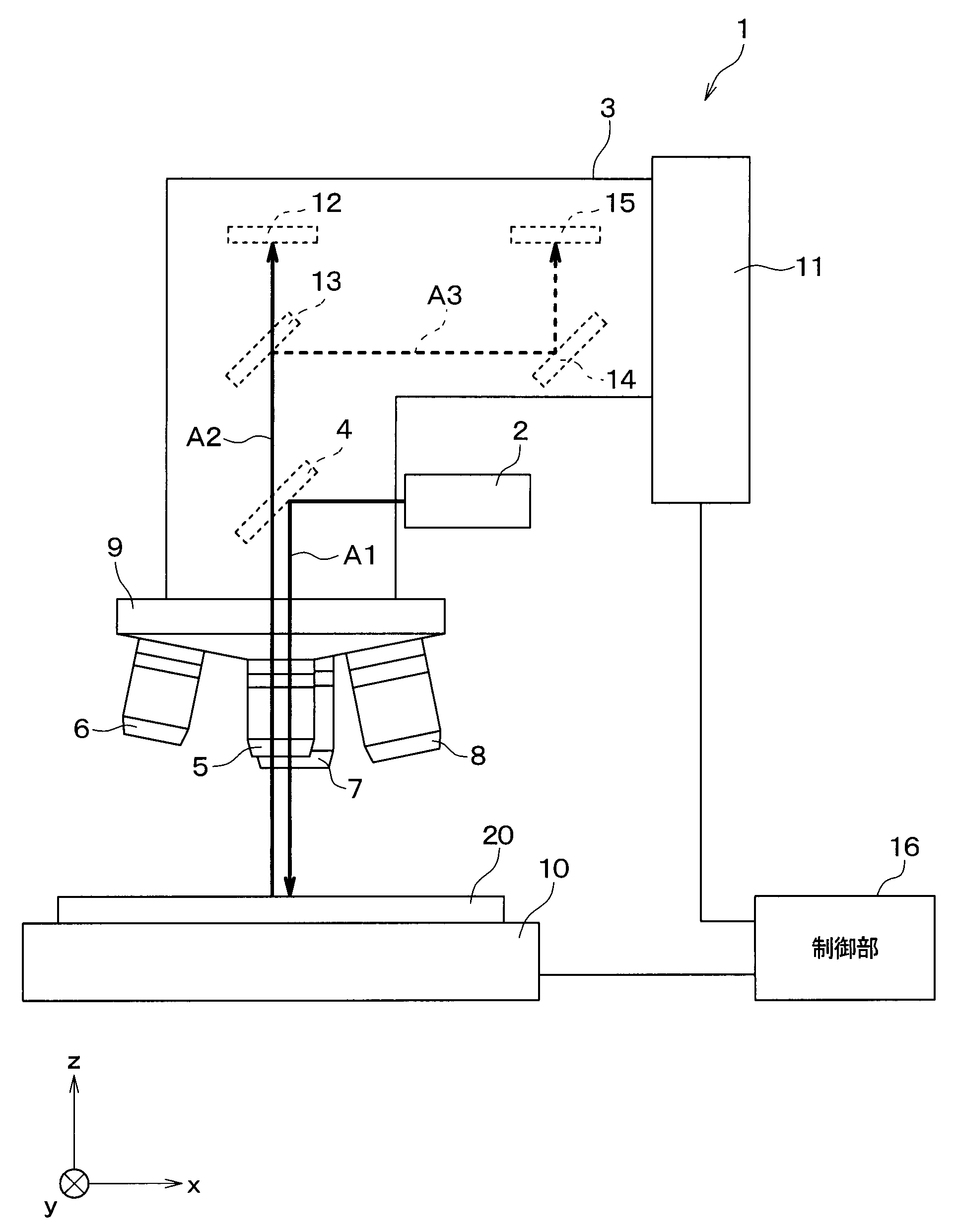
A first embodiment will be described. The
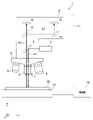
図1に示すように、検査装置1は、光源2と、筐体3と、ハーフミラー4と、第1レンズ5と、第2レンズ6と、第3レンズ7と、第4レンズ8と、回転部9とを備えている。また、検査装置1は、ステージ10と、高さ調整部11と、第1検出部12と、可動ミラー13と、ミラー14と、第2検出部15と、制御部16とを備えている。
As shown in FIG. 1, the
光源2は、検査光を発生させて、この検査光を検査対象である基板に照射するものである。この検査対象の基板は、図1に示すウェハ20、または、後述する基板31である。本実施形態では、検査光は可視光とされ、光源2は例えばキセノンフラッシュランプで構成される。光源2には、制御部16から信号が入力されるようになっており、光源2が発生させる検査光の強度および波長は、制御部16からの入力信号によって設定される。光源2は、筐体3の外壁に配置されており、光源2が発生させた検査光は、筐体3の内部に入射する。
The
筐体3の内部には、ハーフミラー4、第1検出部12、可動ミラー13、ミラー14、第2検出部15が配置されている。光源2が射出した検査光は、ハーフミラー4に入射する。
A
ハーフミラー4は、入射した光の一部を反射し、残りを透過させるものである。ハーフミラー4は、光源2が射出した検査光を反射してウェハ20に照射するように配置されている。ハーフミラー4で反射した検査光は、矢印A1で示すように、筐体3の下部に配置された第1レンズ5、第2レンズ6、第3レンズ7、第4レンズ8のいずれかを通って射出され、ステージ10に載置されたウェハ20または基板31に照射される。ウェハ20または基板31で反射した検査光は、第1レンズ5~第4レンズ8のいずれかを通って筐体3に入射する。
The
第1レンズ5、第2レンズ6、第3レンズ7、第4レンズ8は、ウェハ20または基板31に照射されて反射した検査光を捕捉するものである。第1レンズ5は、ウェハ20の表面の欠陥を検査する際に用いられるレンズである。第1レンズ5の倍率は、例えば5倍とされている。
The
第2レンズ6は、ウェハ20の内部および裏面の欠陥を検査する際に用いられるレンズである。第2レンズ6は、開口数が第1レンズ5よりも小さく、焦点深度が第1レンズ5よりも大きくされている。第2レンズ6の倍率は、例えば5倍とされている。
The
第3レンズ7、第4レンズ8は、第1レンズ5、第2レンズ6を用いた検査で欠陥が見つかった箇所を詳細に観察するためのレンズであり、第1レンズ5、第2レンズ6よりも倍率が高くされている。例えば、第3レンズ7の倍率は10倍または20倍とされ、第4レンズ8の倍率は50倍とされている。
The
第1レンズ5~第4レンズ8は、筐体3の下部に配置された回転部9に取り付けられている。回転部9は、使用するレンズを設定するためのものである。回転部9は、制御部16に接続されており、制御部16からの入力信号によって駆動する。第1レンズ5~第4レンズ8は回転部9の底面に取り付けられており、回転部9が回転することによって、使用するレンズが第1レンズ5~第4レンズ8のいずれかに設定される。
The
なお、図1では、使用するレンズとして第1レンズ5が選択された状態を示しており、矢印A1で示すように第1レンズ5を通って筐体3から射出した検査光が、ウェハ20で反射し、矢印A2で示すように第1レンズ5を通って筐体3に入射している。選択されたレンズによって捕捉された反射光は、矢印A2で示すように、ハーフミラー4を透過して、第1検出部12または可動ミラー13に入射する。
Note that FIG. 1 shows a state in which the
第1レンズ5~第4レンズ8とウェハ20、基板31との位置関係は、ステージ10および高さ調整部11によって調整される。ステージ10は、検査対象の基板を保持するものである。ステージ10の上面の一部は、検査対象の基板が載置される平坦な載置面となっている。図1では、載置面にウェハ20が載置された様子を示している。後述する半導体チップ30を検査する際には、同様に半導体チップ30の基板31が載置面に載置される。
The positional relationship between the
ステージ10の載置面に平行で互いに垂直な2方向を、それぞれx方向、y方向とする。高さ方向、すなわち、x方向、y方向の両方に垂直な方向をz方向とする。ステージ10の載置面は、ステッピングモータ等で構成された図示しないリニアアクチュエータによって、x、y方向に動くようになっている。そして、このように載置面が動くことで、載置面に載置されたウェハ20、基板31がx、y方向に移動する。これにより、第1レンズ5~第4レンズ8に対するウェハ20、基板31のx、y方向の位置が調整される。
The two directions parallel to the mounting surface of the
また、ステージ10の載置面の角度は、図示しないステッピングモータ等によって変化するようになっている。そして、載置面の角度が変化することで、載置面に載置されたウェハ20、基板31の角度が調整される。ステージ10は、制御部16に接続されており、載置面の位置と角度は、制御部16からの入力信号によって設定される。
Further, the angle of the mounting surface of the
第1レンズ5~第4レンズ8とウェハ20、基板31とのz方向の位置関係は、高さ調整部11によって調整される。高さ調整部11は、第1レンズ5~第4レンズ8とウェハ20との距離を複数通りに調整するように構成されている。例えば、高さ調整部11は、ステッピングモータ等で構成されたリニアアクチュエータとされている。そして、筐体3は高さ調整部11に取り付けられており、高さ調整部11の駆動によって筐体3の高さが変わり、第1レンズ5~第4レンズ8とウェハ20、基板31とのz方向の距離が変化する。高さ調整部11は制御部16に接続されており、この距離は制御部16からの入力信号によって設定される。
The positional relationship in the z direction between the
第1検出部12は、第1レンズ5、第2レンズ6によって捕捉された反射光を検出するものである。第1検出部12は、例えば高感度CCD(Charge Coupled Device)等の画像センサを備えたモノクロカメラで構成されている。第1検出部12は、制御部16に接続されており、第1検出部12による反射光の検出結果は、制御部16に送信される。
The
可動ミラー13は、図示しない駆動部によって移動可能とされている。第1レンズ5、第2レンズ6を用いてウェハ20、基板31を検査する際には、ハーフミラー4を透過した光が第1検出部12に入射するように、可動ミラー13は反射光の経路から外れた場所に配置される。そして、第3レンズ7、第4レンズ8を用いてウェハ20、基板31を詳細に観察する際には、可動ミラー13は、図1で示す場所に移動し、ハーフミラー4を透過した光を反射する。可動ミラー13で反射した光は、矢印A3で示すように、ミラー14で反射して、第2検出部15に入射する。
The
第2検出部15は、第3レンズ7、第4レンズ8によって捕捉された光を検出するものである。第2検出部15は、第1レンズ5、第2レンズ6を用いた検査によって欠陥が見つかった箇所を詳細に観察する際に用いられる。第2検出部15は、例えば、CCD等の画像センサを備えたカラーカメラとされている。第2検出部15は、制御部16に接続されており、第2検出部15による反射光の検出結果は、制御部16に送信される。
The
制御部16は、光源2、ステージ10等を操作するとともに、第1検出部12による検出結果等に基づいてウェハ20および基板31の異常判定を行うものであり、判定部に相当する。
The
具体的には、前述したように制御部16は高さ調整部11に接続されており、高さ調整部11は制御部16からの信号によって駆動し、第1レンズ5、第2レンズ6とウェハ20との距離を複数通りに調整する。第1検出部12は、該複数通りに調整された距離それぞれについて、第1レンズ5または第2レンズ6によって捕捉された光を検出する。そして、制御部16は、該複数通りに調整された距離それぞれについての第1検出部12による検出結果に基づいて、ウェハ20の異常判定を行う。
Specifically, as described above, the
また、制御部16は、半導体チップ30の検査工程では、光源2が発生させた光の強度、および、第1検出部12によって検出された光の強度に基づいて、基板31の光の反射率を算出し、該算出した反射率に基づいて基板31の異常判定を行う。
In the inspection process of the
制御部16は、図示しないCPU、ROM、RAM、不揮発性リライタブルメモリ、等を有するマイクロコンピュータを備えている。不揮発性リライタブルメモリは、例えば、EEPROM、フラッシュROM、等である。EEPROMはElectronically Erasable and Programmable Read Only Memoryの略である。制御部16は、内蔵メモリに記憶されたプログラムに従って、光源2等を操作し、ウェハ20等の検査を実行する。
The
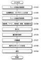
検査装置1による半導体基板の検査方法について説明する。まず、半導体装置の製造工程について説明する。半導体装置の製造工程では、図2に示すステップS101~ステップS109の処理が順に行われる。なお、ここでは、ウェハ20にMOSFET(Metal Oxide Semiconductor Field Effect Transistor)等の半導体素子を形成する場合について説明する。
A method of inspecting a semiconductor substrate by the
ステップS101では、ウェハ20を所望の枚数でウェハロットへ編成し、ウェハ20の結晶欠陥を検査し、検出された欠陥の種類と位置情報を取得する。ステップS101の詳細については後述する。
In step S101, a desired number of
ステップS102では、ウェハ20に拡散層を形成する。また、ウェハ20の耐圧を保持するために、ウェハ20よりも低濃度のエピタキシャル成長を行う。なお、トレンチ構造では、高濃度のエピタキシャル成長を行い、半導体素子の構造を形成していく。
In step S<b>102 , a diffusion layer is formed on the
ステップS103では、ステップS101と同様に、ウェハ20の結晶欠陥を検査し、検出された欠陥の種類と位置情報を取得する。なお、ステップS103では、ステップS102でエピタキシャル成長によってウェハ20に形成された層についても検査を行う。
In step S103, similar to step S101, the
ステップS104では、ウェハ20に拡散層、ゲート、層間膜、配線、保護膜等を形成する。これにより、ウェハ20上に複数の半導体素子が形成される。
In step S104, the
ステップS105では、ウェハ20を個片化して複数の半導体チップ30を形成する。具体的には、ウェハ20に形成された複数の半導体素子の間には、スクライブ領域が形成されており、ステップS105では、このスクライブ領域をダイシングソー等で削って、ウェハ20をチップ単位に分割する。これにより、後述する図6に示す半導体チップ30が複数形成される。
In step S<b>105 , the
ステップS106では、半導体チップ30の電気特性検査を行う。ステップS107では、半導体チップ30の表面の外観検査を行う。ステップS108では、個片化によって半導体チップ30に生じたダメージの検査を行い、ダメージが検出された半導体チップ30の情報を取得する。ステップS108の詳細については後述する。
In step S106, the
ステップS109では、ステップS101、ステップS103、ステップS106~ステップS108の検査結果に基づいて、半導体チップ30を選別する。具体的には、いずれかの検査で異常があると判定された半導体チップ30を除外し、他の半導体チップ30を出荷する。出荷された半導体チップ30は、樹脂封止等を行う組付工程に提供される。このように、異常が検出された半導体チップ30を除外することで、不具合の発生を抑制する。
In step S109, the semiconductor chips 30 are selected based on the inspection results in steps S101, S103, and steps S106 to S108. Specifically, the semiconductor chips 30 determined to be abnormal in any of the inspections are excluded, and the
ステップS101、ステップS103の詳細について説明する。ウェハ20の表面および裏面には、露光時のデフォーカスにより、パターン荒れが生じる場合がある。また、ステップS102におけるエピタキシャル成長の際に、部材の劣化による昇華が起こることがある。また、ウェハ20の反りによりガスが回り込み、裏面荒れが生じる場合がある。また、ウェハ20がSiCで構成される場合には、実効的なC/Si比の乱れにより、カーボンインクルージョンが発生することがある。また、マイクロパイプのような基板を貫通する空孔欠陥が生じることがある。
Details of steps S101 and S103 will be described. Pattern roughness may occur on the front and back surfaces of the
ステップS101、ステップS103では、図3に示すステップS201~ステップS208によって、このようなウェハ20の表面、裏面のパターン荒れや、内部の欠陥の検査を行う。
In steps S101 and S103, such pattern roughness on the front and rear surfaces of the
ステップS201~ステップS203では、ウェハ20の最表面の結晶欠陥とパターン荒れの検査を行う。ステップS201にて、制御部16は、回転部9を操作して、使用するレンズを第1レンズ5に設定する。また、制御部16は、図示しない駆動部を操作して、可動ミラー13をウェハ20からの反射光の経路から外れた位置に移動させる。
In steps S201 to S203, the outermost surface of the
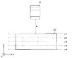
続くステップS202にて、制御部16は、高さ調整部11を操作して、第1レンズ5の高さを調整する。ここでは、第1レンズ5の焦点を、図4のz1で示す位置、すなわち、ウェハ20の表面の高さに合わせるように、第1レンズ5のウェハ20表面からの高さhを調整する。これにより、ウェハ20の表面で反射した検査光が第1レンズ5によって良好に捕捉されるようになる。
In subsequent step S<b>202 , the
続くステップS203にて、制御部16は、ウェハ20の最表面全体をスキャンする。具体的には、制御部16は、光源2を操作してウェハ20に検査光を照射する。そして、制御部16は、ステージ10を操作してウェハ20が置かれた載置面をx、y方向に動かし、ウェハ20の検査対象となる領域を第1レンズ5の下に移動させる。ウェハ20で反射した検査光は、第1レンズ5によって捕捉され、第1検出部12で検出される。制御部16は、このようなウェハ20の移動と反射光の検出とを繰り返す。ウェハ20のx、y方向の全体について反射光の検出が完了すると、x、y方向の各位置についての第1検出部12による検出結果が、制御部16に送信される。その後、処理はステップS204に移行する。
In subsequent step S<b>203 , the
ステップS204~ステップS207では、ウェハ20の内部の欠陥と、裏面のパターン荒れの検査を行う。ステップS204にて、制御部16は、回転部9を操作して、使用するレンズを第2レンズ6に設定する。続くステップS205にて、制御部16は、高さ調整部11を操作して、第2レンズ6の高さを調整する。具体的には、制御部16は、第2レンズ6の高さを低くする。
In steps S204 to S207, defects inside the
続くステップS206にて、制御部16は、ステップS203と同様にスキャンを行う。すなわち、制御部16は、ステージ10を操作してウェハ20が置かれた載置面をx、y方向に動かし、ウェハ20の検査対象となる領域を第2レンズ6の下に移動させる。ウェハ20で反射した検査光は、第2レンズ6によって捕捉され、第1検出部12で検出される。制御部16は、このようなウェハ20の移動と反射光の検出とを繰り返す。ウェハ20のx、y方向の全体について反射光の検出が完了すると、x、y方向の各位置についての第1検出部12による検出結果が、制御部16に送信される。その後、処理はステップS207に移行する。ステップS207にて、制御部16は、ウェハ20の裏面までスキャンが完了したか否かを判定する。
In subsequent step S206, the
ウェハ20の裏面までスキャンが完了していないと判定されると、処理はステップS205に移行し、第2レンズ6の高さがさらに低くなる。具体的には、1回目のステップS205では、第2レンズ6の焦点を図4のz2で示す位置に合わせるように、第2レンズ6の高さが調整される。同様に、2回目のステップS205では、第2レンズ6の焦点をz3で示す位置に合わせるように第2レンズ6の高さが調整され、3回目のステップS205では、第2レンズ6の焦点をz4で示す位置に合わせるように第2レンズ6の高さが調整される。そして、4回目のステップS205では、第2レンズ6の焦点を、z5で示す位置、すなわち、ウェハ20の裏面の高さに合わせるように、第2レンズ6の高さが調整される。そして、z5で示す位置に焦点を合わせた状態でステップS206の処理が完了すると、ウェハ20の裏面までスキャンが完了したと判定される。
If it is determined that scanning has not been completed up to the back surface of the
このように、ウェハ20の内部については、第2レンズ6のz方向の位置が3通りに調整され、z方向のそれぞれの位置において、ウェハ20のx、y方向における全面スキャンが行われる。ウェハ20の裏面までスキャンが完了したと判定されると、処理はステップS208に移行する。
In this way, the
ステップS208にて、制御部16は、ステップS203およびステップS206で第1検出部12から送信されたz1~z5それぞれについての検出結果に基づいて、ウェハ20の異常判定を行う。すなわち、制御部16は、第1レンズ5によって捕捉された光の検出結果、および、第2レンズ6によって捕捉された光の検出結果に基づいて、ウェハ20の異常判定を行う。具体的には、制御部16には、第1検出部12によって撮影されたウェハ20の画像が送信され、制御部16は、この画像を解析して、パターン荒れや結晶欠陥等の異常があるか否かを判定する。
In step S208, the
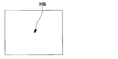
例えば、制御部16には、図5に示すような画像が送信される。図の左右方向、上下方向はそれぞれx、y方向である。図5に示すように画像に黒色の部分が存在すると、その位置に欠陥等の異常が存在すると判定される。そして、z1~z5のいずれかの位置で欠陥等が検出された場合には、制御部16は、ウェハ20のうち、その欠陥が含まれる部分のx、y方向の位置を記憶する。画像に黒色の部分が存在しなければ、そのx、y方向の位置には欠陥等の異常が存在しないと判定される。
For example, an image as shown in FIG. 5 is transmitted to the
さらに本実施形態では、制御部16は、表面と内部の検査結果を統合して、結晶欠陥の種類を識別する。例えば、ウェハ20のうちz1~z4のすべての位置において、図5に示すように欠陥が撮像されると、そのx、y方向の位置については、ウェハ20の表面から内部に至って形成されたカーボンインクルージョンが存在すると判定される。
Furthermore, in this embodiment, the
ウェハ20のうち、異常があると判定された部分については、第3レンズ7または第4レンズ8を用いた詳細な観察が行われる。この観察では、制御部16は、図示しない駆動部を操作して、可動ミラー13を図1に示す位置に移動させる。これにより、反射光が第2検出部15に入射するようになる。そして、第2検出部15によってウェハ20の詳細な画像が撮像され、制御部16に送信される。ステップS208の後、処理は終了する。
A detailed observation using the
このように、ステップS101とステップS103では、制御部16は、ウェハ20の表面のパターン荒れ、内部の結晶欠陥、裏面のパターン荒れの検査を行い、異常がある場所を把握する。
As described above, in steps S101 and S103, the
ステップS101とステップS103のうちステップS101のみを行ってもよいが、ステップS103のように、素子形成工程の途中で検査を行えば、不良が多発する工程を特定することができる。これにより、異物の低減や、露光時のデフォーカスによるパターニング崩れの低減を図ることができる。そして、ウェハ20の品質を向上させることができる。また、ステップS101とステップS103のうち、ステップS103のみを行ってもよい。
Of steps S101 and S103, only step S101 may be performed, but if inspection is performed during the element formation process as in step S103, it is possible to specify a process in which defects frequently occur. As a result, it is possible to reduce the amount of foreign matter and the patterning collapse due to defocusing during exposure. And the quality of the
なお、図3に示す検査工程では、制御部16から光源2へ入力される信号によって、光源2が発生させる検査光の波長が設定され、ウェハ20に吸収されない波長の光が検査光として用いられる。例えば、ウェハ20がSiCで構成されている場合には、ウェハ20に波長500nm以上800nm以下の光が照射される。また、ウェハ20がSiで構成されている場合には、ウェハ20に波長1100nm以上1200nm以下の光が照射される。また、ウェハ20がC(炭素)で構成されている場合には、波長300nm以上600nm以下の光がウェハ20に照射される。
In the inspection process shown in FIG. 3, the wavelength of the inspection light generated by the
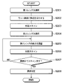
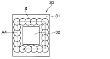
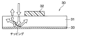
ステップS108の詳細について説明する。ここでは、図6に示す半導体チップ30を検査する場合について説明する。図6に示すように、半導体チップ30は、基板31と、ポリイミド膜32と、電極33とを備えている。基板31は、ウェハ20を矩形状に分割することで形成されたものである。ポリイミド膜32は、図2のステップS104で形成された保護膜であり、図示しない配線層等を覆うように、基板31の表面側に形成されている。電極33は、ステップS104で形成されたものであり、基板31の裏面全体を覆っている。
Details of step S108 will be described. Here, the case of inspecting the
図2のステップS105では、ダイシングラインにクラックやチッピング等のダメージが発生することがある。ステップS109で、このようなダメージが発生した半導体チップを出荷し、樹脂封止等を行う組付工程に提供すると、樹脂封止での熱ストレス等によってダメージが進展して半導体素子が破壊され、機能不全が生じるおそれがある。この素子破壊を抑制するために、ステップS108にてクラック等のダメージを検出し、ダメージが検出された半導体チップをステップS109で除外する。 In step S105 of FIG. 2, damage such as cracks and chipping may occur on the dicing line. In step S109, when the semiconductor chip in which such damage occurs is shipped and provided to an assembly process in which resin sealing or the like is performed, the damage progresses due to heat stress or the like in the resin sealing, and the semiconductor element is destroyed. Dysfunction may occur. In order to suppress this element destruction, damage such as cracks is detected in step S108, and the semiconductor chip in which the damage is detected is excluded in step S109.
ステップS108では、制御部16は、図7に示すステップS301~ステップS305によって、基板31を検査する。まず、ステップS301にて、制御部16は、図示しない搬送装置を操作して、図示しないチップトレイに収納された複数の半導体チップ30から1つをピックアップし、ステージ10に載置する。そして、制御部16は、ステージ10を操作して載置面の角度を調整し、半導体チップ30の平行合わせをする。また、制御部16は、回転部9を操作して、使用するレンズを第1レンズ5または第2レンズ6に設定する。また、制御部16は、図示しない駆動部を操作して、可動ミラー13を半導体チップ30からの反射光の経路から外れた位置に移動させる。
In step S108, the
続くステップS302にて、制御部16は、光源2を操作して基板31に検査光を照射する。検査光は基板31で反射し、ステップS301で設定されたレンズによって捕捉される。そして、制御部16は、このレンズによって捕捉された反射光の強度を第1検出部12で検出しながら、ステージ10を操作して基板31をx、y方向に移動させ、図8に示すように検査光を走査する。図8において、矢印A4は、検査光の走査経路を示している。なお、ステップS302では、第1レンズ5または第2レンズ6が用いられる。
In subsequent step S302, the
検査光は、基板31の上面側から、半導体素子とチップ端部との間の領域に照射される。例えば、検査光は、半導体素子の上層膜であるポリイミド膜32と、基板31の端部であるダイシングラインとの間であって、基板31の端部から数十μm離れた位置に照射される。そして、制御部16は、基板31の角部を照射開始地点として、ポリイミド膜32の周囲を回るように基板31の外周部の4辺を検査光で走査し、1周して照射開始地点に戻ると走査を終了する。
Inspection light is applied from the upper surface side of the
検査光の照射スポットSの直径は、例えば25μmとされるが、場合により約10μmまで小さくしてもよい。また、検査光の走査ステップ、すなわち、隣り合う2つの照射スポットSの中心間の距離は、例えば10μmとされるが、場合により1μm~20μmの間で変化させてもよい。 The diameter of the irradiation spot S of the inspection light is, for example, 25 μm, but may be as small as about 10 μm in some cases. Also, the scanning step of the inspection light, that is, the distance between the centers of two adjacent irradiation spots S is, for example, 10 μm, but may be varied between 1 μm and 20 μm depending on the situation.
続くステップS303にて、制御部16は、図示しない搬送装置を操作して、ステージ10の上の半導体チップ30を図示しないチップトレイに戻す。続くステップS304にて、制御部16は、図示しないチップトレイに収納されたすべての半導体チップ30について、ステップS302のスキャン処理が完了したか否かを判定する。
In subsequent step S303, the
すべての半導体チップ30についてスキャン処理が完了していないと判定されると、処理はステップS301に移行する。そして、図示しないチップトレイに収納された複数の半導体チップ30から、スキャン処理の完了していない1つの半導体チップ30がピックアップされて、ステージ10に載置される。すべての半導体チップ30についてスキャン処理が完了したと判定されると、処理はステップS305に移行する。
If it is determined that the scanning process has not been completed for all
ステップS305にて、制御部16は、各半導体チップ30の異常判定を行う。具体的には、制御部16は、各半導体チップ30について、ステップS302で光源2に発生させた光の強度と、第1検出部12によって検出された反射光の強度とに基づいて、基板31の光の反射率を算出する。そして、制御部16は、該算出した反射率に基づいて基板31の異常判定を行う。反射率は、例えば図9に示すようになる。図9の横軸は検査光を走査した距離であり、ここでは、1つの半導体チップ30の1辺を走査した分の反射率の算出結果を図示している。
At step S<b>305 , the
検査光の一部は基板31の表面で反射して基板31の上方に進み、残りの一部は基板31の内部を進んで電極33で反射し、基板31の内部を通って基板31の表面から上方に射出される。図10の白矢印で示すように、基板31にダメージが発生していない正常部では、検査光があまり散乱せずにまっすぐ進むため、検出される反射光の強度が、高い値でほぼ一定となる。これにより、算出される反射率が、高い値でほぼ一定となる。
A part of the inspection light is reflected by the surface of the
一方、クラックやチッピング等のダメージがある異常部では、図11の白矢印で示すように、検査光が基板31の内部のダメージによって散乱するため、基板31の表面から上方へ射出される光の強度が低下する。これにより、算出される反射率が、正常部に比べて低下する。
On the other hand, in an abnormal portion with damage such as cracks or chipping, the inspection light is scattered due to the damage inside the
この反射率の低下から、ダメージを検出することができる。例えば図9の破線で囲まれた部分は、正常部に対応しており、反射率が高い値でほぼ一定となっている。一方、一点鎖線で囲まれた部分は、ダメージが発生した異常部に対応しており、正常部に対応する部分に比べて、反射率が大きく低下している。このように反射率の低下が検出されると、制御部16は、該当する半導体チップ30に異常があると判定する。一方、半導体チップ30の全体で反射率が高い値でほぼ一定であれば、制御部16は該当する半導体チップ30に異常がないと判定する。
Damage can be detected from this decrease in reflectance. For example, the portion surrounded by the dashed line in FIG. 9 corresponds to the normal portion, and the reflectance is substantially constant at a high value. On the other hand, the portion surrounded by the dashed-dotted line corresponds to the damaged abnormal portion, and the reflectance is significantly lower than the portion corresponding to the normal portion. When a decrease in reflectance is detected in this manner, the
反射率の低下は、例えば、算出された反射率と所定の閾値との比較によって検出される。この閾値は、半導体チップ30に対する樹脂封止以降の応力と素子破壊との相関から決定される。
A decrease in reflectance is detected, for example, by comparing the calculated reflectance with a predetermined threshold. This threshold value is determined from the correlation between the stress on the
なお、反射率の下がり方は、欠陥の種類によって変化する。例えば図9では、チッピングによる反射率の低下を示しているが、他のダメージがある場合には、反射率が図9に示すグラフとは異なる下がり方をする。また、基板に結晶欠陥がある場合にも反射率が低下するが、この場合には、反射率がチッピング等のダメージがある場合とは異なる下がり方をする。具体的には、ダメージがある場合と結晶欠陥がある場合との両方で反射率が低下するが、ダメージがある場合には、反射率がより大きく低下し、ほぼ0になる。制御部16は、反射率の低下を検出すると、さらに、反射率の下がり方から、欠陥の種類を判定する。例えば、正常な基板の反射率の標準偏差をσとして、制御部16は、反射率の低下を検出すると、その反射率が3σ値から外れた場合に、チッピング等のダメージが存在すると判定する。
It should be noted that how the reflectance decreases varies depending on the type of defect. For example, FIG. 9 shows a drop in reflectance due to chipping, but if there is other damage, the reflectance drops differently from the graph shown in FIG. The reflectance also decreases when the substrate has crystal defects, but in this case, the reflectance decreases in a manner different from that when there is damage such as chipping. Specifically, the reflectance decreases both when there is damage and when there is a crystal defect, but when there is damage, the reflectance decreases more greatly and becomes almost zero. When detecting a decrease in reflectance, the
異常があると判定された半導体チップ30については、第3レンズ7または第4レンズ8を用いた詳細な観察が行われる。この観察では、可動ミラー13が図1に示す位置に移動して、反射光が第2検出部15に入射するようになる。そして、第2検出部15によって半導体チップ30の詳細な画像が撮像され、制御部16に送信される。すべての半導体チップ30について異常判定が完了すると、制御部16は処理を終了する。
A detailed observation using the
なお、図7に示す工程においても、図3に示す工程と同様に、基板31に吸収されない波長の光が検査光として用いられる。すなわち、基板31がSiCで構成されている場合には、基板31に波長500nm以上800nm以下の光が照射される。また、基板31がSiで構成されている場合には、基板31に波長1100nm以上1200nm以下の光が照射される。また、基板31がCで構成されている場合には、波長300nm以上600nm以下の光が基板31に照射される。
In the process shown in FIG. 7, light having a wavelength that is not absorbed by the
以上説明したように、本実施形態では、半導体チップ30に検査光を照射し、検査光の反射率に基づいて異常判定を行っている。そして、クラック等のダメージが含まれる基板では、正常な基板に比べて光の反射率が低下する。また、反射率の下がり方は、欠陥の種類によって変わる。したがって、上記のように反射率を算出することで、欠陥の種類を識別することが可能になり、結晶状態を良好に把握することができる。
As described above, in the present embodiment, the
また、上記実施形態によれば、以下のような効果を得ることができる。 Moreover, according to the above embodiment, the following effects can be obtained.
(1)第2レンズ6とウェハ20との距離を複数通りに調整し、複数通りに調整された距離それぞれについての第1検出部12による検出結果に基づいて、ウェハ20の異常判定を行っている。複数の検出結果を統合することにより、例えば、ウェハ20の表層部のみに存在する欠陥と、ウェハ20の厚さ方向の全体にわたって存在する欠陥とを識別することが可能になり、結晶状態をさらに良好に把握することができる。
(1) The distance between the
(2)第1レンズ5でウェハ20の表面からの反射光を捕捉し、第1レンズ5よりも焦点深度の大きい第2レンズ6でウェハ20の内部と裏面からの反射光を捕捉している。これにより、ウェハ20の表面の欠陥を検査する際に、ウェハ20の裏面やステージ10の映り込みを抑制するとともに、ウェハ20の内部および裏面の欠陥を検出することが可能になり、欠陥の種類の識別精度が向上する。
(2) The
(3)検査対象の基板に吸収されない波長の光が検査光として用いられる。これにより、欠陥を良好に捕捉することが可能になり、異常判定の精度が向上する。 (3) Light having a wavelength that is not absorbed by the substrate to be inspected is used as the inspection light. As a result, defects can be captured well, and the accuracy of abnormality determination is improved.
(他の実施形態)
なお、本発明は上記した実施形態に限定されるものではなく、特許請求の範囲に記載した範囲内において適宜変更が可能である。また、上記実施形態において、実施形態を構成する要素は、特に必須であると明示した場合および原理的に明らかに必須であると考えられる場合等を除き、必ずしも必須のものではないことは言うまでもない。また、上記実施形態において、実施形態の構成要素の個数、数値、量、範囲等の数値が言及されている場合、特に必須であると明示した場合および原理的に明らかに特定の数に限定される場合等を除き、その特定の数に限定されるものではない。
(Other embodiments)
It should be noted that the present invention is not limited to the above-described embodiments, and can be appropriately modified within the scope of the claims. Further, in the above-described embodiments, it goes without saying that the elements constituting the embodiments are not necessarily essential, except when explicitly stated as being essential or when they are considered to be clearly essential in principle. . In addition, in the above embodiments, when numerical values such as the number, numerical value, amount, range, etc. of the constituent elements of the embodiment are mentioned, when it is explicitly stated that they are essential, and when they are clearly limited to a specific number in principle It is not limited to that particular number, except when
例えば、上記第1実施形態では、可視光を検査光として用いたが、不可視光を検査光として用いてもよい。例えば、赤外光を検査光として用いてもよい。また、図3に示す検査工程と図7に示す検査工程の両方を行うことで、基板の状態をより良好に把握することができるが、これらの検査工程のうち一方のみを行ってもよい。 For example, in the first embodiment, visible light is used as inspection light, but invisible light may be used as inspection light. For example, infrared light may be used as inspection light. By performing both the inspection process shown in FIG. 3 and the inspection process shown in FIG. 7, the state of the substrate can be better grasped, but only one of these inspection processes may be performed.
また、上記第1実施形態では、高さ調整部11によって第1レンズ5、第2レンズ6とウェハ20との距離を調整したが、ステージ10の載置面をz方向に動かすことによって、この距離を複数通りに調整してもよい。例えば、ステッピングモータ等で構成されたリニアアクチュエータによって、載置面をz方向に動かすことができる。このようにステージ10によって上記の距離を複数通りに調整する場合には、ステージ10は調整部に相当する。
In the first embodiment, the distance between the
また、上記第1実施形態では、第1レンズ5、第2レンズ6の高さを合わせて5通りに調整したが、この高さを2~4通りに調整してもよいし、6通り以上に調整してもよい。すなわち、第2レンズ6の高さを1~3通りに調整してもよいし、5通り以上に調整してもよい。
In addition, in the first embodiment, the heights of the
また、上記第1実施形態では、ウェハ20の検査対象となる場所によって第1レンズ5と第2レンズ6とを使い分けているが、いずれか一方のレンズでウェハ20の表面から裏面までを検査してもよい。例えば、第1レンズ5を用いてウェハ20の表面から裏面までを検査すると、反射光を鮮明に捕捉することのできる範囲が狭くなるが、複数の位置における検査結果を統合することで、欠陥の種類をある程度の精度で識別することができる。
In the first embodiment, the
また、ステップS101、S103の結果に基づいて、異常のある半導体チップ30を除外し、他の半導体チップ30についてのみステップS106~S109を行ってもよいし、すべての半導体チップ30についてステップS106~S109を行ってもよい。すべての半導体チップ30についてステップS106等を行う場合には、反射率の下がり方から、基板31の異常がウェハ20に存在した結晶欠陥であるかダイシングによるダメージであるかを識別することができる。
Further, based on the results of steps S101 and S103, the
本開示に記載の制御部及びその手法は、コンピュータプログラムにより具体化された一つ乃至は複数の機能を実行するようにプログラムされたプロセッサ及びメモリを構成することによって提供された専用コンピュータにより、実現されてもよい。あるいは、本開示に記載の制御部及びその手法は、一つ以上の専用ハードウエア論理回路によってプロセッサを構成することによって提供された専用コンピュータにより、実現されてもよい。もしくは、本開示に記載の制御部及びその手法は、一つ乃至は複数の機能を実行するようにプログラムされたプロセッサ及びメモリと一つ以上のハードウエア論理回路によって構成されたプロセッサとの組み合わせにより構成された一つ以上の専用コンピュータにより、実現されてもよい。また、コンピュータプログラムは、コンピュータにより実行されるインストラクションとして、コンピュータ読み取り可能な非遷移有形記録媒体に記憶されていてもよい。 The controller and techniques described in this disclosure may be implemented by a dedicated computer provided by configuring a processor and memory programmed to perform one or more functions embodied by the computer program. may be Alternatively, the controls and techniques described in this disclosure may be implemented by a dedicated computer provided by configuring the processor with one or more dedicated hardware logic circuits. Alternatively, the control units and techniques described in this disclosure can be implemented by a combination of a processor and memory programmed to perform one or more functions and a processor configured by one or more hardware logic circuits. It may also be implemented by one or more dedicated computers configured. The computer program may also be stored as computer-executable instructions on a computer-readable non-transitional tangible recording medium.
2 光源
5 第1レンズ
6 第2レンズ
10 ステージ
11 高さ調整部
12 第1検出部
16 制御部
2
Claims (11)
光を発生させて検査対象である基板に照射する光源(2)と、
前記基板に照射されて反射した光を捕捉するレンズ(5、6)と、
前記レンズによって捕捉された光を検出する検出部(12)と、
前記光源が発生させた光の強度、および、前記検出部によって検出された光の強度に基づいて、前記基板の光の反射率を算出し、該算出した反射率に基づいて前記基板の異常判定を行う判定部(16)と、を備える半導体基板の検査装置。 A semiconductor substrate inspection device,
a light source (2) for generating light to irradiate a substrate to be inspected;
Lenses (5, 6) for capturing the light irradiated and reflected by the substrate;
a detector (12) for detecting light captured by said lens;
Calculate the light reflectance of the substrate based on the intensity of the light generated by the light source and the intensity of the light detected by the detection unit, and determine the abnormality of the substrate based on the calculated reflectance A semiconductor substrate inspection device, comprising: a determination unit (16) for performing
前記検出部は、該複数通りに調整された距離それぞれについて、前記レンズによって捕捉された光を検出し、
前記判定部は、
該算出した反射率に基づいて前記基板の異常判定を行うとともに、
該複数通りに調整された距離それぞれについての前記検出部による検出結果に基づいて、前記基板の異常判定を行う請求項1に記載の半導体基板の検査装置。 An adjusting unit (10, 11) for adjusting the distance between the substrate and the lens in a plurality of ways,
the detector detects light captured by the lens for each of the plurality of adjusted distances;
The determination unit
Determining abnormality of the substrate based on the calculated reflectance,
2. The apparatus for inspecting a semiconductor substrate according to claim 1, wherein abnormality determination of the substrate is performed based on the detection results of the detection unit for each of the distances adjusted in the plurality of ways.
光を発生させて検査対象である基板に照射する光源(2)と、
前記基板に照射されて反射した光を捕捉するレンズ(5、6)と、
前記基板と前記レンズとの距離を複数通りに調整する調整部(10、11)と、
該複数通りに調整された距離それぞれについて、前記レンズによって捕捉された光を検出する検出部(12)と、
該複数通りに調整された距離それぞれについての前記検出部による検出結果に基づいて、前記基板の異常判定を行う判定部(16)と、を備える半導体基板の検査装置。 A semiconductor substrate inspection device,
a light source (2) for generating light to irradiate a substrate to be inspected;
Lenses (5, 6) for capturing the light irradiated and reflected by the substrate;
adjustment units (10, 11) for adjusting the distance between the substrate and the lens in a plurality of ways;
a detector (12) for detecting light captured by said lens for each of said plurality of adjusted distances;
A semiconductor substrate inspection apparatus, comprising: a determination unit (16) that determines an abnormality of the substrate based on detection results of the detection unit for each of the plurality of adjusted distances.
2つの前記レンズをそれぞれ第1レンズ(5)、第2レンズ(6)として、
前記第2レンズは、前記第1レンズよりも焦点深度が大きくされており、
前記判定部は、前記調整部によって前記第1レンズの焦点が前記基板の表面に合わせられたときの前記検出部による検出結果、および、前記調整部によって前記第2レンズの焦点が前記基板の内部または裏面に合わせられたときの前記検出部による検出結果に基づいて、前記基板の異常判定を行う請求項2または3に記載の半導体基板の検査装置。 Equipped with two said lenses,
The two lenses are respectively a first lens (5) and a second lens (6),
The second lens has a greater depth of focus than the first lens,
The determination unit determines a result of detection by the detection unit when the focus of the first lens is adjusted to the surface of the substrate by the adjustment unit, and a result of detection by the detection unit when the focus of the second lens is adjusted to the inside of the substrate by the adjustment unit. 4. The apparatus for inspecting a semiconductor substrate according to claim 2 or 3, wherein abnormality determination of said substrate is performed based on a result of detection by said detection unit when it is aligned with the back surface.
検査対象である基板に光を照射することと、
前記基板に照射されて反射した光をレンズ(5、6)によって捕捉することと、
前記レンズによって捕捉された光を検出することと、
前記基板に照射した光の強度、および、該検出された光の強度に基づいて、前記基板の光の反射率を算出し、該算出した反射率に基づいて前記基板の異常判定を行うことと、を備える半導体基板の検査方法。 A semiconductor substrate inspection method comprising:
irradiating a substrate to be inspected with light;
Capturing by lenses (5, 6) the light irradiated and reflected by the substrate;
detecting light captured by the lens;
calculating the light reflectance of the substrate based on the intensity of the light irradiated to the substrate and the intensity of the detected light, and performing abnormality determination of the substrate based on the calculated reflectance; A semiconductor substrate inspection method comprising:
該複数通りに調整された距離それぞれについて、前記レンズによって捕捉された光を検出することと、
該検出することにおける該複数通りに調整された距離それぞれについての検出結果に基づいて、前記基板の異常判定を行うことと、を備える請求項5に記載の半導体基板の検査方法。 adjusting the distance between the substrate and the lens in a plurality of ways;
detecting light captured by the lens for each of the plurality of adjusted distances;
6. The method of inspecting a semiconductor substrate according to claim 5, further comprising determining an abnormality of the substrate based on detection results for each of the plurality of distances adjusted in the detection.
検査対象である基板に光を照射することと、
前記基板に照射されて反射した光をレンズ(5、6)によって捕捉することと、
前記基板と前記レンズとの距離を複数通りに調整することと、
該複数通りに調整された距離それぞれについて、前記レンズによって捕捉された光を検出することと、
該検出することにおける該複数通りに調整された距離それぞれについての検出結果に基づいて、前記基板の異常判定を行うことと、を備える半導体基板の検査方法。 A semiconductor substrate inspection method comprising:
irradiating a substrate to be inspected with light;
Capturing by lenses (5, 6) the light irradiated and reflected by the substrate;
adjusting the distance between the substrate and the lens in a plurality of ways;
detecting light captured by the lens for each of the plurality of adjusted distances;
A method of inspecting a semiconductor substrate, comprising determining an abnormality of the substrate based on detection results for each of the plurality of adjusted distances in the detection.
該調整することの後、前記基板に照射されて反射した光を前記第1レンズによって捕捉することと、
前記第1レンズによって捕捉された光を検出することと、
前記第1レンズよりも焦点深度の大きい第2レンズ(6)の焦点が前記基板の内部または裏面に合うように前記基板と前記第2レンズとの距離を調整することと、
該調整することの後、前記基板に照射されて反射した光を前記第2レンズによって捕捉することと、
前記第2レンズによって捕捉された光を検出することと、
前記第1レンズによって捕捉された光の検出結果、および、前記第2レンズによって捕捉された光の検出結果に基づいて、前記基板の異常判定を行うことと、を備える請求項6または7に記載の半導体基板の検査方法。 adjusting the distance between the substrate and the first lens so that the focus of the first lens (5) matches the surface of the substrate;
After the adjusting, capturing the reflected light from the substrate with the first lens;
detecting light captured by the first lens;
adjusting the distance between the substrate and the second lens so that the focal point of the second lens (6), which has a greater depth of focus than the first lens, is aligned with the inside or the back surface of the substrate;
After the adjusting, capturing the reflected light from the substrate with the second lens;
detecting light captured by the second lens;
8. The method according to claim 6, further comprising determining an abnormality of the substrate based on a detection result of the light captured by the first lens and a detection result of the light captured by the second lens. and a semiconductor substrate inspection method.
前記照射することでは、前記基板に波長が500nm以上800nm以下の光を照射する請求項5ないし8のいずれか1つに記載の半導体基板の検査方法。 The substrate is made of silicon carbide,
9. The semiconductor substrate inspection method according to claim 5, wherein the irradiating includes irradiating the substrate with light having a wavelength of 500 nm or more and 800 nm or less.
前記照射することでは、前記基板に波長が1100nm以上1200nm以下の光を照射する請求項5ないし8のいずれか1つに記載の半導体基板の検査方法。 The substrate is made of silicon,
9. The method of inspecting a semiconductor substrate according to claim 5, wherein the irradiating includes irradiating the substrate with light having a wavelength of 1100 nm or more and 1200 nm or less.
前記照射することでは、前記基板に波長が300nm以上600nm以下の光を照射する請求項5ないし8のいずれか1つに記載の半導体基板の検査方法。 The substrate is made of carbon,
9. The method of inspecting a semiconductor substrate according to claim 5, wherein the irradiating includes irradiating the substrate with light having a wavelength of 300 nm or more and 600 nm or less.
Priority Applications (4)
| Application Number | Priority Date | Filing Date | Title |
|---|---|---|---|
| JP2021003631A JP2022108564A (en) | 2021-01-13 | 2021-01-13 | Inspection apparatus and inspection method for semiconductor substrate |
| PCT/JP2021/046050 WO2022153763A1 (en) | 2021-01-13 | 2021-12-14 | Device for inspecting semiconductor substrate and inspection method |
| CN202180090108.2A CN116710760A (en) | 2021-01-13 | 2021-12-14 | Semiconductor substrate inspection device and inspection method |
| US18/329,792 US12546726B2 (en) | 2021-01-13 | 2023-06-06 | Inspection apparatus and inspection method for semiconductor substrate |
Applications Claiming Priority (1)
| Application Number | Priority Date | Filing Date | Title |
|---|---|---|---|
| JP2021003631A JP2022108564A (en) | 2021-01-13 | 2021-01-13 | Inspection apparatus and inspection method for semiconductor substrate |
Publications (1)
| Publication Number | Publication Date |
|---|---|
| JP2022108564A true JP2022108564A (en) | 2022-07-26 |
Family
ID=82447205
Family Applications (1)
| Application Number | Title | Priority Date | Filing Date |
|---|---|---|---|
| JP2021003631A Pending JP2022108564A (en) | 2021-01-13 | 2021-01-13 | Inspection apparatus and inspection method for semiconductor substrate |
Country Status (4)
| Country | Link |
|---|---|
| US (1) | US12546726B2 (en) |
| JP (1) | JP2022108564A (en) |
| CN (1) | CN116710760A (en) |
| WO (1) | WO2022153763A1 (en) |
Cited By (1)
| Publication number | Priority date | Publication date | Assignee | Title |
|---|---|---|---|---|
| JP2024017766A (en) * | 2022-07-28 | 2024-02-08 | 株式会社デンソー | Silicon carbide semiconductor device manufacturing system and silicon carbide semiconductor device manufacturing method |
Citations (6)
| Publication number | Priority date | Publication date | Assignee | Title |
|---|---|---|---|---|
| JPH06308040A (en) * | 1993-04-22 | 1994-11-04 | Matsushita Electric Ind Co Ltd | Foreign matter inspection device |
| JPH07198619A (en) * | 1993-12-28 | 1995-08-01 | Ratotsuku Syst Eng Kk | Crystal defect detecting method by using forward scattered light |
| JP2008096314A (en) * | 2006-10-12 | 2008-04-24 | Nikon Corp | Macro inspection device |
| JP2009032795A (en) * | 2007-07-25 | 2009-02-12 | Rohm Co Ltd | Method of manufacturing nitride semiconductor light emitting element |
| JP2009099820A (en) * | 2007-10-18 | 2009-05-07 | Fujitsu Microelectronics Ltd | Inspection device, inspection method, and semiconductor device manufacturing method |
| JP2010219114A (en) * | 2009-03-13 | 2010-09-30 | Tokyo Institute Of Technology | Carbon electrode, method for manufacturing the same, organic transistor and method for manufacturing the same |
Family Cites Families (12)
| Publication number | Priority date | Publication date | Assignee | Title |
|---|---|---|---|---|
| JPH10256326A (en) * | 1997-03-07 | 1998-09-25 | Sharp Corp | Pattern inspection method and inspection device |
| JPH11160230A (en) * | 1997-11-28 | 1999-06-18 | Mitsubishi Materials Silicon Corp | Method and apparatus for detecting crystal defect near surface |
| US7312921B2 (en) * | 2004-02-27 | 2007-12-25 | Hamamatsu Photonics K.K. | Microscope and sample observation method |
| US7586607B2 (en) | 2006-04-21 | 2009-09-08 | Rudolph Technologies, Inc. | Polarization imaging |
| JP2009182244A (en) * | 2008-01-31 | 2009-08-13 | Sharp Corp | Manufacturing method of solar cell module |
| JP5544894B2 (en) * | 2010-01-21 | 2014-07-09 | カシオ計算機株式会社 | Wafer inspection apparatus and wafer inspection method |
| US20110242312A1 (en) * | 2010-03-30 | 2011-10-06 | Lasertec Corporation | Inspection system and inspection method |
| JP2012134310A (en) * | 2010-12-21 | 2012-07-12 | Fujitsu Semiconductor Ltd | Defect inspection method, defect inspection device, and defect inspection system |
| KR20140114169A (en) * | 2013-03-18 | 2014-09-26 | 삼성전자주식회사 | Apparatus and method for estimating the depth of the buried defect in the substrate |
| US9696264B2 (en) * | 2013-04-03 | 2017-07-04 | Kla-Tencor Corporation | Apparatus and methods for determining defect depths in vertical stack memory |
| JP2019160999A (en) | 2018-03-13 | 2019-09-19 | 株式会社アイテス | Defect inspection device, and defect inspection method |
| KR102459337B1 (en) * | 2020-12-21 | 2022-10-28 | 주식회사 에타맥스 | Die Division Method and Inspection Apparatus Avoiding Defects Locations on Silicon Carbide Wafers |
-
2021
- 2021-01-13 JP JP2021003631A patent/JP2022108564A/en active Pending
- 2021-12-14 WO PCT/JP2021/046050 patent/WO2022153763A1/en not_active Ceased
- 2021-12-14 CN CN202180090108.2A patent/CN116710760A/en active Pending
-
2023
- 2023-06-06 US US18/329,792 patent/US12546726B2/en active Active
Patent Citations (6)
| Publication number | Priority date | Publication date | Assignee | Title |
|---|---|---|---|---|
| JPH06308040A (en) * | 1993-04-22 | 1994-11-04 | Matsushita Electric Ind Co Ltd | Foreign matter inspection device |
| JPH07198619A (en) * | 1993-12-28 | 1995-08-01 | Ratotsuku Syst Eng Kk | Crystal defect detecting method by using forward scattered light |
| JP2008096314A (en) * | 2006-10-12 | 2008-04-24 | Nikon Corp | Macro inspection device |
| JP2009032795A (en) * | 2007-07-25 | 2009-02-12 | Rohm Co Ltd | Method of manufacturing nitride semiconductor light emitting element |
| JP2009099820A (en) * | 2007-10-18 | 2009-05-07 | Fujitsu Microelectronics Ltd | Inspection device, inspection method, and semiconductor device manufacturing method |
| JP2010219114A (en) * | 2009-03-13 | 2010-09-30 | Tokyo Institute Of Technology | Carbon electrode, method for manufacturing the same, organic transistor and method for manufacturing the same |
Cited By (2)
| Publication number | Priority date | Publication date | Assignee | Title |
|---|---|---|---|---|
| JP2024017766A (en) * | 2022-07-28 | 2024-02-08 | 株式会社デンソー | Silicon carbide semiconductor device manufacturing system and silicon carbide semiconductor device manufacturing method |
| JP7835134B2 (en) | 2022-07-28 | 2026-03-25 | 株式会社デンソー | Manufacturing system for silicon carbide semiconductor devices and method for manufacturing silicon carbide semiconductor devices |
Also Published As
| Publication number | Publication date |
|---|---|
| US20230314342A1 (en) | 2023-10-05 |
| US12546726B2 (en) | 2026-02-10 |
| CN116710760A (en) | 2023-09-05 |
| WO2022153763A1 (en) | 2022-07-21 |
Similar Documents
| Publication | Publication Date | Title |
|---|---|---|
| KR102038478B1 (en) | Wafer inspection method and wafer inspection apparatus | |
| CN109564172B (en) | Defect inspection apparatus, defect inspection method, die bonder, semiconductor manufacturing method, and semiconductor device manufacturing method | |
| JP5137088B2 (en) | Mold removal method | |
| US11244842B2 (en) | Processing apparatus for detecting defects inside electronic component including illumination portion and imaging portion | |
| CN109382591B (en) | Laser processing method | |
| JP4973062B2 (en) | Semiconductor chip inspection method and wafer crack inspection apparatus | |
| US20240416450A1 (en) | Processing method and processing system | |
| JP2018004378A (en) | Automated imaging device | |
| JP6595130B2 (en) | Defect detection device, defect detection method, die bonder, semiconductor manufacturing method, and semiconductor device manufacturing method | |
| JP7769859B2 (en) | Workpiece inspection method and device | |
| JP7219400B2 (en) | WORK INSPECTION METHOD AND APPARATUS AND WORK MACHINING METHOD | |
| KR20240148891A (en) | Processing method and processing system | |
| US12546726B2 (en) | Inspection apparatus and inspection method for semiconductor substrate | |
| CN119688708A (en) | System, method and computer readable storage medium for detecting wafer cracks | |
| CN112204384A (en) | Dicing chip inspection device | |
| WO2018131101A1 (en) | Charged particle beam device and optical examination device | |
| WO2017074256A1 (en) | Method and system to detect chippings on solar wafer | |
| US20120224051A1 (en) | Mask inspection method and mask inspection apparatus | |
| KR102575267B1 (en) | Apparatus and method for inspecting chipping in wafer | |
| US8625090B2 (en) | Method and apparatus for inspecting substrates | |
| JP2007333491A (en) | Appearance inspection device for plate | |
| JP2009267306A (en) | Inspection device | |
| JP2024130080A (en) | Observation method, microscope, and processing device | |
| JP5094048B2 (en) | Appearance inspection device | |
| JP2008020371A (en) | Inspection device |
Legal Events
| Date | Code | Title | Description |
|---|---|---|---|
| A621 | Written request for application examination |
Free format text: JAPANESE INTERMEDIATE CODE: A621 Effective date: 20221219 |
|
| A131 | Notification of reasons for refusal |
Free format text: JAPANESE INTERMEDIATE CODE: A131 Effective date: 20240220 |
|
| A02 | Decision of refusal |
Free format text: JAPANESE INTERMEDIATE CODE: A02 Effective date: 20240820 |