JP2021022572A - Led lighting device for animal/plant growth, led lighting module for animal/plant growth, shelf board for animal/plant growth shelf, animal/plant growth shelf, and animal/plant growth factory - Google Patents
Led lighting device for animal/plant growth, led lighting module for animal/plant growth, shelf board for animal/plant growth shelf, animal/plant growth shelf, and animal/plant growth factory Download PDFInfo
- Publication number
- JP2021022572A JP2021022572A JP2020174214A JP2020174214A JP2021022572A JP 2021022572 A JP2021022572 A JP 2021022572A JP 2020174214 A JP2020174214 A JP 2020174214A JP 2020174214 A JP2020174214 A JP 2020174214A JP 2021022572 A JP2021022572 A JP 2021022572A
- Authority
- JP
- Japan
- Prior art keywords
- led lighting
- plants
- led
- growing
- light
- Prior art date
- Legal status (The legal status is an assumption and is not a legal conclusion. Google has not performed a legal analysis and makes no representation as to the accuracy of the status listed.)
- Pending
Links
Images


Classifications
-
- Y—GENERAL TAGGING OF NEW TECHNOLOGICAL DEVELOPMENTS; GENERAL TAGGING OF CROSS-SECTIONAL TECHNOLOGIES SPANNING OVER SEVERAL SECTIONS OF THE IPC; TECHNICAL SUBJECTS COVERED BY FORMER USPC CROSS-REFERENCE ART COLLECTIONS [XRACs] AND DIGESTS
- Y02—TECHNOLOGIES OR APPLICATIONS FOR MITIGATION OR ADAPTATION AGAINST CLIMATE CHANGE
- Y02A—TECHNOLOGIES FOR ADAPTATION TO CLIMATE CHANGE
- Y02A40/00—Adaptation technologies in agriculture, forestry, livestock or agroalimentary production
- Y02A40/10—Adaptation technologies in agriculture, forestry, livestock or agroalimentary production in agriculture
- Y02A40/25—Greenhouse technology, e.g. cooling systems therefor
Landscapes
- Cultivation Of Plants (AREA)
- Fastening Of Light Sources Or Lamp Holders (AREA)
- Arrangement Of Elements, Cooling, Sealing, Or The Like Of Lighting Devices (AREA)
- Planar Illumination Modules (AREA)
- Led Device Packages (AREA)
Abstract
Description
本開示は、動植物育成用のLED照明装置、動植物育成用のLED照明モジュール、動植物の育成棚用の棚板、動植物の育成棚、及び動植物育成工場に関する。 The present disclosure relates to an LED lighting device for growing animals and plants, an LED lighting module for growing animals and plants, a shelf board for growing shelves for animals and plants, a shelf for growing animals and plants, and a plant for growing animals and plants.
動植物育成工場において用いる照明装置として、従来の蛍光灯や高圧ナトリウムランプ等に替えて、近年、消費電力が少ないLEDを光源とする照明装置の需要が拡大している。 In recent years, there has been an increasing demand for lighting devices that use LEDs as a light source, which consume less power, in place of conventional fluorescent lamps, high-pressure sodium lamps, and the like as lighting devices used in animal and plant growing factories.
LEDを光源とする照明装置を用いた動植物育成工場の一例として、植物の育成棚の棚板に、LEDを光源とする直管型の植物育成灯を複数配置した植物育成装置が知られている(例えば特許文献1参照)。 As an example of an animal and plant growing factory using a lighting device using an LED as a light source, a plant growing device in which a plurality of straight tube type plant growing lights using an LED as a light source are arranged on a shelf board of a plant growing shelf is known. (See, for example, Patent Document 1).
フレキシブルタイプの回路基板に複数のLEDチップを配置して面状の光源を形成した動植物育成用のLED照明装置も提案されている(例えば特許文献2参照)。 An LED lighting device for growing animals and plants in which a plurality of LED chips are arranged on a flexible type circuit board to form a planar light source has also been proposed (see, for example, Patent Document 2).
本開示は、動植物を良好な収量で得ることが可能な、動植物育成用のLED照明装置、動植物育成用のLED照明モジュール、動植物の育成棚用の棚板、動植物の育成棚、及び動植物育成工場を提供する。 The present disclosure discloses an LED lighting device for growing animals and plants, an LED lighting module for growing animals and plants, a shelf board for growing shelves for animals and plants, a shelf for growing animals and plants, and a plant for growing animals and plants, which can obtain animals and plants in a good yield. I will provide a.
本実施の形態による動植物育成用のLED照明装置は、複数のLEDチップが配列された、動植物育成用のLED照明装置であって、前記LEDチップの光源色は、JIS Z 9112に規定される光源色のうち、電球色または温白色である。 The LED lighting device for growing animals and plants according to the present embodiment is an LED lighting device for growing animals and plants in which a plurality of LED chips are arranged, and the light source color of the LED chips is a light source specified in JIS Z 9112. Of the colors, it is light bulb color or warm white.
本実施の形態による動植物育成用のLED照明装置において、前記LEDチップの前記光源色が前記電球色であってもよい。 In the LED lighting device for growing animals and plants according to the present embodiment, the light source color of the LED chip may be the light bulb color.
本実施の形態による動植物育成用のLED照明装置は、複数のLEDチップが配列された、動植物育成用のLED照明装置であって、前記LEDチップからの光の発光スペクトルは、中心波長が610nm以上630nm以下である第1のピークと、中心波長が440nm以上460nm以下である第2のピークと、中心波長が510nm以上530nm以下である第3のピークとを有し、前記第1のピークにおける相対発光強度は、前記第2のピークにおける相対発光強度よりも大きく、前記第3のピークにおける相対発光強度は、前記第2のピークにおける相対発光強度よりも小さい。 The LED lighting device for growing animals and plants according to the present embodiment is an LED lighting device for growing animals and plants in which a plurality of LED chips are arranged, and the emission spectrum of light from the LED chips has a center wavelength of 610 nm or more. It has a first peak having a center wavelength of 630 nm or less, a second peak having a center wavelength of 440 nm or more and 460 nm or less, and a third peak having a center wavelength of 510 nm or more and 530 nm or less, and is relative to the first peak. The light emission intensity is larger than the relative light emission intensity at the second peak, and the relative light emission intensity at the third peak is smaller than the relative light emission intensity at the second peak.
本実施の形態による動植物育成用のLED照明装置は、複数のLEDチップが配列された、動植物育成用のLED照明装置であって、前記LEDチップからの光は、中心波長が610nm以上630nm以下であるとともに半値幅が90nm以上110nm以下である第1の成分と、中心波長が440nm以上460nm以下であるとともに半値幅が10nm以上20nm以下である第2の成分と、中心波長が510nm以上530nm以下であるとともに半値幅が50nm以上60nm以下である第3の成分とを有し、前記第1の成分の中心波長における相対発光強度は、前記第2の成分の中心波長における相対発光強度よりも大きく、前記第3の成分の中心波長における相対発光強度は、前記第2の成分の中心波長における相対発光強度よりも小さい。 The LED lighting device for growing animals and plants according to the present embodiment is an LED lighting device for growing animals and plants in which a plurality of LED chips are arranged, and the light from the LED chips has a center wavelength of 610 nm or more and 630 nm or less. A first component having a half-value width of 90 nm or more and 110 nm or less, a second component having a center wavelength of 440 nm or more and 460 nm or less and a half-value width of 10 nm or more and 20 nm or less, and a center wavelength of 510 nm or more and 530 nm or less. It also has a third component having a half-value width of 50 nm or more and 60 nm or less, and the relative emission intensity of the first component at the center wavelength is larger than the relative emission intensity of the second component at the center wavelength. The relative emission intensity of the third component at the center wavelength is smaller than the relative emission intensity of the second component at the center wavelength.
本実施の形態による動植物育成用のLED照明装置において、前記第2の成分の中心波長における相対発光強度は、前記第1の成分の中心波長における相対発光強度の0.5倍以上0.7倍以下であり、前記第3の成分の中心波長における相対発光強度は、前記第1の成分の中心波長における相対発光強度の0.3倍以上0.5倍以下であってもよい。 In the LED lighting device for growing animals and plants according to the present embodiment, the relative emission intensity of the second component at the center wavelength is 0.5 times or more and 0.7 times the relative emission intensity of the first component at the center wavelength. The relative emission intensity of the third component at the center wavelength may be 0.3 times or more and 0.5 times or less of the relative emission intensity of the first component at the center wavelength.
本実施の形態による動植物育成用のLED照明装置は、複数のLEDチップが配列された、動植物育成用のLED照明装置であって、前記LEDチップからの光の色度は、xy色度図において、(0.39,0.36)、(0.41,0.44)、(0.46,0.44)、(0.42,0.36)の4つの色度座標を結ぶ四角形の領域内にある。 The LED lighting device for growing animals and plants according to the present embodiment is an LED lighting device for growing animals and plants in which a plurality of LED chips are arranged, and the chromaticity of light from the LED chips is shown in the xy chromaticity diagram. , (0.39, 0.36), (0.41, 0.44), (0.46, 0.44), (0.42, 0.36) of the square connecting the four chromaticity coordinates. It is in the area.
本実施の形態による動植物育成用のLED照明装置において、前記LEDチップは、10個以上直列に配置され、このLEDチップの列が4列以上並列に配置されていてもよい。 In the LED lighting device for growing animals and plants according to the present embodiment, 10 or more LED chips may be arranged in series, and 4 or more rows of the LED chips may be arranged in parallel.
本実施の形態による動植物育成用のLED照明装置において、前記LEDチップは、透明保護膜によって覆われていてもよい。 In the LED lighting device for growing animals and plants according to the present embodiment, the LED chip may be covered with a transparent protective film.
本実施の形態による動植物育成用のLED照明装置において、基板フィルムと、前記基板フィルムの表面に形成された金属配線部とを備え、前記複数のLEDチップは、前記金属配線部に実装されていてもよい。 The LED lighting device for growing animals and plants according to the present embodiment includes a substrate film and a metal wiring portion formed on the surface of the substrate film, and the plurality of LED chips are mounted on the metal wiring portion. May be good.
本実施の形態による動植物育成用のLED照明装置において、最も厚い部分における厚みが5mm以下であってもよい。 In the LED lighting device for growing animals and plants according to the present embodiment, the thickness at the thickest portion may be 5 mm or less.
本実施の形態による動植物育成用のLED照明モジュールは、動植物育成用のLED照明モジュールであって、本実施の形態による前記動植物育成用のLED照明装置と、前記動植物育成用のLED照明装置に電気的に接続された制御部とを備え、前記制御部は、前記動植物育成用のLED照明装置に対して外付けで接続されたものである。 The LED lighting module for growing animals and plants according to the present embodiment is an LED lighting module for growing animals and plants, and the LED lighting device for growing animals and plants according to the present embodiment and the LED lighting device for growing animals and plants are electrically connected. A control unit is provided, and the control unit is externally connected to the LED lighting device for growing animals and plants.
本実施の形態による動植物育成用のLED照明モジュールにおいて、前記制御部から前記動植物育成用のLED照明装置に定電圧が印加されてもよい。 In the LED lighting module for growing animals and plants according to the present embodiment, a constant voltage may be applied from the control unit to the LED lighting device for growing animals and plants.
本実施の形態による動植物育成用のLED照明モジュールにおいて、前記制御部は、前記LEDチップの調光を制御可能であってもよい。 In the LED lighting module for growing animals and plants according to the present embodiment, the control unit may be able to control the dimming of the LED chip.
本実施の形態による動植物の育成棚用の棚板は、動植物の育成棚用の棚板であって、基板と、前記基板に取り付けられた、本実施の形態による前記動植物育成用のLED照明装置または本実施の形態による前記動植物育成用のLED照明モジュールとを備えている。 The shelf board for growing animals and plants according to the present embodiment is a shelf board for growing animals and plants, and is a substrate and an LED lighting device for growing animals and plants according to the present embodiment attached to the substrate. Alternatively, it is provided with the LED lighting module for growing animals and plants according to the present embodiment.
本実施の形態による動植物の育成棚は、動植物の育成棚であって、棚板を備え、前記棚板は、基板の下面側に取り付けられた、本実施の形態による前記動植物育成用のLED照明装置または本実施の形態による前記動植物育成用のLED照明モジュールとを備えている。 The animal and plant growing shelf according to the present embodiment is an animal and plant growing shelf, and includes a shelf board, and the shelf board is attached to the lower surface side of the substrate and is LED lighting for growing the animals and plants according to the present embodiment. It is provided with an apparatus or an LED lighting module for growing animals and plants according to the present embodiment.
本実施の形態による動植物の育成棚において、前記動植物育成用のLED照明装置は、前記棚板の側面側にも更に配置されていてもよい。 In the animal and plant growing shelf according to the present embodiment, the LED lighting device for growing animals and plants may be further arranged on the side surface side of the shelf board.
本実施の形態による動植物育成工場は、建物と、前記建物の内部に配置された本実施の形態による前記動植物の育成棚とを備えている。 The animal and plant growing factory according to the present embodiment includes a building and a shelf for growing the animals and plants according to the present embodiment arranged inside the building.
本実施の形態によれば、動植物を良好な収量で得ることができる。 According to this embodiment, animals and plants can be obtained in a good yield.
本実施の形態による動植物育成用のLED照明装置は、複数のLEDチップが配列され、LEDチップの光源色は、JIS Z 9112に規定される光源色のうち、電球色または温白色である。 In the LED lighting device for growing animals and plants according to the present embodiment, a plurality of LED chips are arranged, and the light source color of the LED chips is a light bulb color or a warm white color among the light source colors specified in JIS Z 9112.
本実施の形態による動植物育成用のLED照明装置は、LEDチップの光源色が、JIS Z 9112に規定される光源色のうち、電球色または温白色であるので、育成される動植物の収率の低下を抑制しつつ育成される動植物の育成量を増やすことができ、動植物を良好な収量で得られる。ところで、人工光によって植物を栽培する動植物育成工場の主な課題としては、採算性を向上させることが挙げられている。採算性を向上させる要素としては、例えば植物の場合、単価の高い栽培対象物を選定することの他、短期間で大きく育てるための生育促進や、イニシャルコストやランニングコストといったコストの低減等が考えられる。例えば、光合成を促進することにより生育を促進する案として、赤色LEDチップ及び青色LEDチップの2種類のLEDチップを使用した生育コントロール技術がある。しかしながら、2種類のLEDチップを使用する場合、2種類のLEDチップを準備する必要があり、コストの低減を図ることが困難である。また、近年、葉物野菜であっても、緑色の光を吸収して光合成を行うことが証明されている。このため、光源としては、白色LEDチップで十分であり、大量生産されている白色LEDチップを用いたLED照明装置によって植物を効率良く育成することが望まれている。これに対して、本実施の形態によれば、LEDチップの光源色が、JIS Z 9112に規定される光源色のうち、電球色または温白色であるので、植物を効率良く育成することができ、良好な収量が得られる。 In the LED lighting device for growing animals and plants according to the present embodiment, the light source color of the LED chip is a light bulb color or warm white among the light source colors specified in JIS Z 9112, so that the yield of the animals and plants to be grown is increased. It is possible to increase the amount of animals and plants to be cultivated while suppressing the decrease, and the animals and plants can be obtained with a good yield. By the way, improving profitability is mentioned as a main issue of animal and plant growing factories that cultivate plants by artificial light. In the case of plants, for example, in the case of plants, in addition to selecting cultivated objects with a high unit price, growth promotion for large growth in a short period of time, reduction of costs such as initial cost and running cost, etc. are considered as factors to improve profitability. Be done. For example, as a plan for promoting growth by promoting photosynthesis, there is a growth control technique using two types of LED chips, a red LED chip and a blue LED chip. However, when two types of LED chips are used, it is necessary to prepare two types of LED chips, and it is difficult to reduce the cost. In recent years, it has been proved that even leafy vegetables absorb green light and perform photosynthesis. Therefore, a white LED chip is sufficient as a light source, and it is desired to efficiently grow plants by an LED lighting device using a mass-produced white LED chip. On the other hand, according to the present embodiment, since the light source color of the LED chip is a light bulb color or warm white among the light source colors defined in JIS Z 9112, plants can be efficiently grown. , Good yield is obtained.
また、本実施の形態による動植物育成用のLED照明装置は、複数のLEDチップが配列され、LEDチップからの光の発光スペクトルは、中心波長が610nm以上630nm以下である第1のピークと、中心波長が440nm以上460nm以下である第2のピークと、中心波長が510nm以上530nm以下である第3のピークとを有し、前記第1のピークにおける相対発光強度は、前記第2のピークにおける相対発光強度よりも大きく、前記第3のピークにおける相対発光強度は、前記第2のピークにおける相対発光強度よりも小さい。 Further, in the LED lighting device for growing animals and plants according to the present embodiment, a plurality of LED chips are arranged, and the emission spectrum of the light from the LED chips has a center wavelength of 610 nm or more and 630 nm or less. It has a second peak having a wavelength of 440 nm or more and 460 nm or less, and a third peak having a center wavelength of 510 nm or more and 530 nm or less, and the relative light emission intensity at the first peak is relative to the second peak. It is larger than the light emission intensity, and the relative light emission intensity at the third peak is smaller than the relative light emission intensity at the second peak.
本実施の形態による動植物育成用のLED照明装置は、LEDチップ21からの光の発光スペクトルSが、中心波長が610nm以上630nm以下である第1のピークP1と、中心波長が440nm以上460nm以下である第2のピークP2と、中心波長が510nm以上530nm以下である第3のピークP3とを有している。また、第1のピークP1の中心波長における相対発光強度は、第2のピークP2の中心波長における相対発光強度よりも大きく、第3のピークP3の中心波長における相対発光強度は、第2のピークP2の中心波長における相対発光強度よりも小さくなっている。これにより、LEDチップ21からの光が白色になるとともに、LEDチップ21の光源色を電球色または温白色とすることができる。このため、上述した効果を得ることができる。
In the LED lighting device for growing animals and plants according to the present embodiment, the emission spectrum S of the light from the
本実施の形態による動植物育成用のLED照明装置は、複数のLEDチップが配列され、LEDチップからの光は、中心波長が610nm以上630nm以下であるとともに半値幅が90nm以上110nm以下である第1の成分と、中心波長が440nm以上460nm以下であるとともに半値幅が10nm以上20nm以下である第2の成分と、中心波長が510nm以上530nm以下であるとともに半値幅が50nm以上60nm以下である第3の成分とを有し、前記第1の成分の中心波長における相対発光強度は、前記第2の成分の中心波長における相対発光強度よりも大きく、前記第3の成分の中心波長における相対発光強度は、前記第2の成分の中心波長における相対発光強度よりも小さい。 In the LED lighting device for growing animals and plants according to the present embodiment, a plurality of LED chips are arranged, and the light from the LED chips has a center wavelength of 610 nm or more and 630 nm or less and a half width of 90 nm or more and 110 nm or less. And the second component having a center wavelength of 440 nm or more and 460 nm or less and a half-value width of 10 nm or more and 20 nm or less, and a third component having a center wavelength of 510 nm or more and 530 nm or less and a half-value width of 50 nm or more and 60 nm or less. The relative emission intensity of the first component at the center wavelength is larger than the relative emission intensity of the second component at the center wavelength, and the relative emission intensity of the third component at the center wavelength is , It is smaller than the relative emission intensity at the center wavelength of the second component.
本実施の形態による動植物育成用のLED照明装置は、LEDチップ21からの光が、中心波長が610nm以上630nm以下であるとともに半値幅が90nm以上110nm以下である第1の成分C1と、中心波長が440nm以上460nm以下であるとともに半値幅が10nm以上20nm以下である第2の成分C2と、中心波長が510nm以上530nm以下であるとともに半値幅が50nm以上60nm以下である第3の成分C3とを有している。また、第1の成分C1の中心波長における相対発光強度は、第2の成分C2の中心波長における相対発光強度よりも大きく、第3の成分C3の中心波長における相対発光強度は、第2の成分C2の中心波長における相対発光強度よりも小さくなっている。これにより、LEDチップ21からの光が白色になるとともに、LEDチップ21の光源色を電球色または温白色とすることができる。このため、上述した効果を得ることができる。
In the LED lighting device for growing animals and plants according to the present embodiment, the light from the
本実施の形態による動植物育成用のLED照明装置は、複数のLEDチップが配列され、LEDチップからの光の色度は、xy色度図において、(0.39,0.36)、(0.41,0.44)、(0.46,0.44)、(0.42,0.36)の4つの色度座標を結ぶ四角形の領域内にある。 In the LED lighting device for growing animals and plants according to the present embodiment, a plurality of LED chips are arranged, and the chromaticity of the light from the LED chips is (0.39, 0.36), (0) in the xy chromaticity diagram. It is in the area of the quadrangle connecting the four chromaticity coordinates of .41, 0.44), (0.46, 0.44), and (0.42, 0.36).
本実施の形態による動植物育成用のLED照明装置は、LEDチップ21からの光の色度が、xy色度図において、(0.39,0.36)、(0.41,0.44)、(0.46,0.44)、(0.42,0.36)の4つの色度座標を結ぶ四角形の領域内にある。この場合、LEDチップ21からの光が白色になるとともに、LEDチップ21の光源色を電球色または温白色とすることができる。このため、上述した効果を得ることができる。
In the LED lighting device for growing animals and plants according to the present embodiment, the chromaticity of the light from the
また、本実施の形態による動植物育成用のLED照明モジュールは、動植物育成用のLED照明装置と、前記LED照明装置に電気的に接続された制御部と、を備え、前記制御部は、前記LED照明装置に対して外付けで接続されたものである。 Further, the LED lighting module for growing animals and plants according to the present embodiment includes an LED lighting device for growing animals and plants and a control unit electrically connected to the LED lighting device, and the control unit is the LED. It is externally connected to the lighting device.
本実施の形態による動植物育成用のLED照明モジュールは、外付けの制御部を有するので、育成される動植物の収率の低下を抑制しつつ育成される動植物の育成量を増やすことができ、動植物を良好な収量で得られる。制御部付近で局所的に発生する熱は、制御部に近いところで育成されている動植物に強く影響し、制御部から遠いところで育成されている動植物への影響は低い。そのため、動植物の育成状態にばらつきが生じて不適合品が多くなり、収率が低下するおそれがある。制御部が外付けでLED照明装置に対して外付けで接続されたLED照明モジュールによれば、制御部を任意の場所に設置できるので、ばらつきを抑制して良好な収量が得られる。 Since the LED lighting module for growing animals and plants according to the present embodiment has an external control unit, it is possible to increase the amount of animals and plants to be grown while suppressing a decrease in the yield of animals and plants to be grown. Can be obtained with good yield. The heat generated locally near the control unit strongly affects the animals and plants grown near the control unit, and has a low effect on the animals and plants grown far from the control unit. Therefore, there is a risk that the growing state of animals and plants will vary, the number of nonconforming products will increase, and the yield will decrease. According to the LED lighting module in which the control unit is externally connected to the LED lighting device, the control unit can be installed at an arbitrary place, so that variation can be suppressed and a good yield can be obtained.
本実施の形態による動植物の育成棚用の棚板、動植物の育成棚、及び動植物育成工場は、上記の本実施の形態による動植物育成用のLED照明装置またはモジュールを備えるので、動植物を良好な収量で得ることができる。 The shelves for growing animals and plants according to the present embodiment, the shelves for growing animals and plants, and the plant for growing animals and plants are provided with the LED lighting device or module for growing animals and plants according to the above embodiment, so that good yields of animals and plants can be obtained. Can be obtained at.
以下、図面を参照しながら一実施の形態について具体的に説明する。以下に示す各図は、模式的に示したものである。そのため、各部の大きさ、形状は理解を容易にするために、適宜誇張している。また、技術思想を逸脱しない範囲において適宜変更して実施することが可能である。なお、以下に示す各図において、同一部分には同一の符号を付しており、一部詳細な説明を省略する場合がある。また、本明細書中に記載する各部材の寸法等の数値および材料名は、実施の形態としての一例であり、これに限定されるものではなく、適宜選択して使用することができる。本明細書において、形状や幾何学的条件を特定する用語、例えば平行や直交、垂直等の用語については、厳密に意味するところに加え、実質的に同じ状態も含むものとする。本明細書において、動植物とは、動物及び/又は植物を意味する。なお、以下においては、便宜上、LED照明モジュールによって植物を育成(栽培)する場合を例にとって説明するが、矛盾の生じない範囲で、動物を育成する場合にも適用することができる。 Hereinafter, one embodiment will be specifically described with reference to the drawings. Each figure shown below is schematically shown. Therefore, the size and shape of each part are exaggerated as appropriate to facilitate understanding. In addition, it is possible to make appropriate changes within the range that does not deviate from the technical concept. In each of the figures shown below, the same parts are designated by the same reference numerals, and some detailed description thereof may be omitted. Further, numerical values such as dimensions of each member and material names described in the present specification are examples of embodiments, and are not limited to these, and can be appropriately selected and used. In the present specification, terms that specify a shape and geometric conditions, such as parallel, orthogonal, and vertical, are intended to include substantially the same state in addition to the exact meaning. As used herein, the term "animals and plants" means animals and / or plants. In the following, for convenience, a case of growing (cultivating) a plant by an LED lighting module will be described as an example, but it can also be applied to a case of raising an animal within a range where no contradiction occurs.
(植物育成用のLED照明モジュール)
図1に示す、本実施の形態による植物育成用のLED照明モジュール10(以下、LED照明モジュール10ともいう)は、後述するように、人工光を用いた植物育成工場90(図9)内に設置され、植物を育成するものである。このようなLED照明モジュール10は、植物育成用のLED照明シート(LED照明装置)20(以下、LED照明シート20ともいう)と、LED照明シート20に電気的に接続された制御部40とを備えている。
(LED lighting module for growing plants)
The LED lighting module 10 (hereinafter, also referred to as LED lighting module 10) for growing plants according to the present embodiment shown in FIG. 1 is located in a plant growing factory 90 (FIG. 9) using artificial light, as will be described later. It is installed and grows plants. Such an
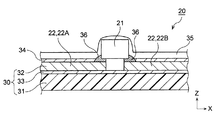
図2に示すように、LED照明シート20は、いわゆる面状の光源シートであり、そのシート面の発光面側(使用時に植物方向を向く側)に複数のLEDチップ21が配列されたものである。このような直下型のLED照明シート20を用いることで、LEDチップ21からの照射光がそのまま発光面を通過して直接直下の植物に到達するので、光量を強くして植物の育成の促進を図ることができ、また、シート全体の厚さを薄くしてLEDチップ21の側部側の影を発生しにくくすることができる。なお、図2では、直下型のLED照明シート20の例を示しているが、これに限定されず、導光板等を介在させたエッジライト型のLED照明シートを用いてもよい。エッジライト型のLED照明シートは、発光面からの光量のばらつきを抑制しやすい。図2のLED照明シート20は、フレキシブル配線基板30と、フレキシブル配線基板30上に規則的に配置された複数のLEDチップ21とを備えている。このようなフレキシブル配線基板30を用いることで、シート面の面積が比較的大きいLED照明シート20を得ることができる。一般に、植物育成工場や植物の育成棚では、LED照明シート20は、複数を配列して使用されるが、隣り合うLED照明シート20どうしの位置がばらつくと光量のばらつきが生じて植物の収率が低下するおそれがある。シート面の面積が比較的大きいLED照明シート20は、使用するLED照明シート20の数を減らすことができるので、複数のLED照明シート20の配置による光量のばらつきを抑制することができる。なお、図2では、フレキシブル配線基板30を備えたLED照明シート20の例を示しているが、これに限定されず、リジット配線基板を備えたLED照明シートを用いてもよい。リジット配線基板を備えたLED照明シートは、応力による耐性が高く、破損しにくい。なお、図2において、後述する光反射性絶縁保護膜34及び透明保護膜35の表示を省略している。
As shown in FIG. 2, the
この場合、LEDチップ21は、フレキシブル配線基板30内で平面視で格子点状に配置されている。すなわちLEDチップ21は、マトリックス状に多段多列に配置されており、直列にM個接続されたLEDチップ21の列RがN列配置されている。例えば図2において、LEDチップ21は、LEDチップ21の第1の配列方向(X方向)に沿って、14個(M=14)直列に接続されている。さらに、この14個のLEDチップ21をもつ列Rが、LEDチップ21の第2の配列方向(Y方向)に沿って、10列(N=10)並列に配置されている。なお、LEDチップ21の配置数はこれに限られるものではない。具体的には、LEDチップ21を、第1の配列方向(X方向)に10個以上14個以下(14≧M≧10)直列に配置し、この列RをLEDチップ21の第2の配列方向(Y方向)に4列以上10列以下(10≧N≧4)並列に配置することが好ましい。LEDチップ21を10個以上直列に配置することにより、LEDチップ21を第1の配列方向(X方向)に沿って短い間隔で配置することができ、LED照明シート20の照度の面内ばらつきを抑えることができ、植物に照射する光のばらつきを抑制することができる。LEDチップ21を14個以下直列に配置することにより、消費電力を削減することができ、植物育成工場90における光熱費等のランニングコストを低減することができる。また、LEDチップ21の列をLEDチップ21の第2の配列方向(Y方向)に4列以上並列に配置することにより、特定のLEDチップ21が破損した場合でも、他の列のLEDチップ21に波及しないようにし、LED照明シート20全体の照度が極端に低下することを抑止することができる。また、LED照明シート20の照度が低下した範囲を限定することで、不適合品が発生するおそれがある範囲を限定し、収率の低下を抑制することができる。また、LED照明シート20が直下型の場合には、設置や清掃のときにLEDチップ21に誤って強く接触して破損するおそれが高まるため、破損時の対策を行っておくことは、リスク管理の観点で重要である。さらに、LEDチップ21の列を10列以下並列に配置することにより、消費電力を削減することができ、植物育成工場90における光熱費等のランニングコストを低減することができる。
In this case, the LED chips 21 are arranged in a grid pattern in the
LED照明シート20は、複数の金属配線部22を有し、複数の金属配線部22は、第1の配列方向(X方向)に沿って配列されている。第1の配列方向(X方向)に沿って配列された複数の金属配線部22は、それぞれLEDチップ21の各列Rに対応している。LEDチップ21は、それぞれX方向に互いに隣接する一対の金属配線部22同士を跨ぐように配置されている。またLEDチップ21の図示しない各端子は、一対の金属配線部22にそれぞれ電気的に接続されている。複数の金属配線部22は、LEDチップ21への給電部を構成しており、複数の金属配線部22に電力が供給されることにより、当該列Rに配置されたLEDチップ21が全て点灯する。なお、複数の金属配線部22は、後述する金属配線部32の一部を構成する。
The
第1の配列方向(X方向)におけるLEDチップ21同士の間隔Pxは、37mm以上50mm以下とすることが好ましい。また、第2の配列方向(Y方向)におけるLEDチップ21同士の間隔Pyは、37mm以上100mm以下とすることが好ましい。LEDチップ21同士の間隔を上記範囲とすることにより、LED照明シート20の輝度を面内で均一にして、植物に照射する光のばらつきを抑制するとともに、LED照明シート20の消費電力を抑えることができる。
The distance Px between the LED chips 21 in the first arrangement direction (X direction) is preferably 37 mm or more and 50 mm or less. Further, the distance Py between the LED chips 21 in the second arrangement direction (Y direction) is preferably 37 mm or more and 100 mm or less. By setting the distance between the LED chips 21 to the above range, the brightness of the
LED照明シート20のうち最も厚い部分における厚みは、5mm以下とすることが好ましい。このようにLED照明シート20の厚みを薄くすることにより、LED照明シート20を設置する基板81(図10)同士の上下方向の間隔を狭くすることができ、これにより各植物の育成棚80(図10)あたりの基板81の数を増やすことができる。この結果、単位面積あたりの植物の収穫量を増やすことができる。また、植物とLED照明シート20が近接しているときに植物に照射される比較的強い光のばらつきをより抑制できる。
The thickness of the thickest portion of the
LEDチップ21の配列は、平面視格子点状に限られるものではなく、図3(a)に示すように、平面視で千鳥状に配置されていても良い。また、LEDチップ21は、LED照明シート20の面内で均一に配置されていなくても良い。例えば、LED照明シート20の周縁部において、LEDチップ21の密度をより高めても良い。具体的には、図3(b)に示すように、LED照明シート20の中央部(図3(b)の下部)でLEDチップ21を格子点状に配置し、LED照明シート20の周縁部(図3(b)の上部)でLEDチップ21を千鳥状に配置しても良い。これにより、LED照明シート20の周縁部におけるLED照明シート20の輝度の低下を抑制し、LED照明シート20の輝度を面内で均一にして、植物に照射する光のばらつきを抑制することができる。
The arrangement of the LED chips 21 is not limited to the point shape of the grid in a plan view, and may be arranged in a staggered pattern in a plan view as shown in FIG. 3 (a). Further, the LED chips 21 do not have to be uniformly arranged in the plane of the
LED照明シート20の全体形状は、平面視長方形形状となっているが、LED照明シート20のサイズや平面形状については特に限定されるものではない。LED照明シート20は、サイズや形状の加工の自由度が高いため、この点に関する様々な需要に対しても柔軟に対応することが可能である。また、その可撓性を活かして、フラットな設置面に限らず様々な形状の設置面への取付けが可能である。また、LED照明シート20自体が剛性をもっているため、例えばLED照明シート20をLEDチップ21が外側になる様に円筒状に曲げることによって、設置面がなくとも、LED照明シート20単体で照明とすることも可能である。
The overall shape of the
図2において、LED照明シート20の第1の配列方向(X方向)の長さLxは、500mm以上700mm以下とすることが好ましく、550mm以上650mm以下とすることが更に好ましい。LED照明シート20の第2の配列方向(Y方向)の長さLyは、300mm以上500mm以下とすることが好ましく、350mm以上450mm以下とすることが更に好ましい。LED照明シート20の大きさを上記範囲とすることにより、LED照明シート20を一般的な植物育成用の基板81(図10)に適合させることができ、基板81のデッドスペースを減らすことができる。また、個々のLED照明シート20の大きさが過度に大きすぎないことにより、特定のLEDチップ21が破損した場合に、他のLEDチップ21に影響が及ぶことを最低限に抑え、植物の育成棚用の棚板83(図10)全体の照度が極端に低下することを防止しかつ照度が低下する範囲を限定することができる。
In FIG. 2, the length Lx of the
次に、制御部40について説明する。図1に示すように、制御部40は、LED照明シート20に電力を供給するとともに、LED照明シート20の発光等を制御するものである。この制御部40は、LED照明シート20上に設けられた第1コネクタ44Aを介してLED照明シート20に対して着脱自在に接続される。すなわち制御部40は、LED照明シート20と別体に構成され、LED照明シート20に対して外付けで接続されるようになっている。すなわち制御部40は、LED照明シート20と一体化されていない。これにより、熱源となる制御部40をLED照明シート20から分離することができ、制御部40からの熱によって植物の生育に影響を及ぼさないようにすることができる。
Next, the
また制御部40は、電力入力部41と、AC/DCコンバーター(ドライバー)42と、PWM制御部43とを有している。このうち電力入力部41には、例えば100V乃至240Vの任意の電圧をもつ交流の電圧が供給される。AC/DCコンバーター42は、100V乃至240Vの交流電圧を定圧(例えば44V)の直流電圧に変換する。PWM制御部43は、AC/DCコンバーター42からの定電圧波形のパルス幅を任意に変化させることにより、LED照明シート20のLEDチップ21の調光を行うものである。すなわちPWM制御部43は、LED照明シート20の調光を制御する調光制御部としての役割も果たす。PWM制御部43から出力される定電圧は、第1コネクタ44Aを介してLED照明シート20に印加される。
Further, the
制御部40のPWM制御部43からLED照明シート20に定電圧が印加されることにより、LED照明シート20に直接整流化されたパルス電圧が印加される場合と異なり、LEDチップ21の調光を行うことが可能となる。すなわち、PWM制御部43は、AC/DCコンバーター42からの直流電圧のデューティー比を適宜変化させることにより、LEDチップ21の照度を任意に制御することができる。例えば、図4(a)に示すように、PWM制御部43は、AC/DCコンバーター42からの定電圧のデューティー比を100%(実線)から50%(点線)に抑えることにより、LEDチップ21の照度を低下させることができる。
By applying a constant voltage to the
このようにLEDチップ21の照度を適宜調節することにより、植物の生育ステージに応じてLED照明シート20の照度を調節し、植物の生育の度合いを調整することができる。例えば、植物の葉の小さい生育初期には、LED照明シート20の照度を低くし、植物の葉の大きい生育後期には、LED照明シート20の照度を高くしても良い。あるいは、植物の背丈の低い生育初期には、植物とLEDチップ21との距離が離れているため、LED照明シート20の照度を高くし、植物の背丈の大きい生育後期には、植物とLEDチップ21との距離が近づくため、LED照明シート20の照度を低くしても良い。LED照明シート20の照度調整の他の例としては、高い照度が必要な種類の植物のときは照度を高くし、低い照度でも育成できる種類の植物のときは照度を低くても良い。出荷の時期を早めたいときは照度を高くし、出荷の時期を遅らせたいときは照度を低くしても良い。
By appropriately adjusting the illuminance of the
また、PWM制御部43からLED照明シート20に定電圧が印加されることにより、LED照明シート20からの光の単位時間あたりの積算光量を増加することができる。すなわち、例えば、LED照明シート20に定電圧が印加された場合における積算光量(図4(a)の網掛け部分の面積)を、比較例としてパルスで電圧が印加される場合における積算光量(図4(b)の網掛け部分の面積)よりも大きくすることができる。これにより、LED照明シート20からの光の発光効率を高め、植物の育成効率を向上させることができる。
Further, by applying a constant voltage from the
再度図1を参照すると、LED照明シート20には、レギュレータ45が設けられている。この場合、レギュレータ45は、LEDチップ21の各列に対応してそれぞれ設けられており、具体的には、10列のLEDチップ21の列に対応して10個のレギュレータ45が設けられている。このレギュレータ45は、各列の複数のLEDチップ21に流れる電流を一定に保持する役割を果たす。これにより、1つのLEDチップ21が破損した場合でも、他の列のLEDチップ21に過大な電流が流れることを抑え、他の列のLEDチップ21が破損しないようにすることができる。この結果、LED照明シート20全体の照度が極端に低下することを防止することができ、植物に照射する光のばらつきを抑制することができる。また、レギュレータ45は接続する抵抗値により制御する電流量を列ごとに制御可能であり、たとえば、最初の列と最後の列の制御用抵抗値を変化させることで、周辺部の列のみ出力をあげることができる。これにより、通常、LED照明シート20同士を隙間なく敷き詰めることで均一性を確保する狙いがあるが、コストの観点や通気性確保の観点で、LED照明シート20間を5cm〜10cm程度あけたとしても、その継ぎ目が消せる効果が期待できる。
Referring to FIG. 1 again, the
さらに、LED照明シート20には、第1コネクタ44Aから分岐して電力供給ライン46が設けられている。また、LED照明シート20上には第2コネクタ44Bが設けられている。電力供給ライン46は、当該LED照明シート20のLEDチップ21には電気的に接続されることなく、LED照明シート20と同一の構成をもつ他のLED照明シート200の配線に対して電気的に接続される。すなわち電力供給ライン46は、第2コネクタ44B及び他のLED照明シート200上に設けられた他の第1コネクタ44Aを介して、LED照明シート200の配線に着脱自在に接続される。電力供給ライン46からの電流は、第2コネクタ44B及び他の第1コネクタ44Aを介して、他のLED照明シート200に供給される。これにより、2つのLED照明シート20、200を連結し、これら2つのLED照明シート20、200を1つの制御部40によって同時に制御することができる。1つの制御部40によって複数のLED照明シート20、200を同時に制御することができることによって、熱の発生源である制御部40の数を減らすことができるので、制御部40からの熱による植物の育成のばらつきが発生しにくくなって収量の低下を抑制することができる。
Further, the
(LED照明シートの各部材)
次に、LED照明シート20を構成する各部材について説明する。図5に示すように、LED照明シート20は、フレキシブル配線基板30と、フレキシブル配線基板30上に配置された複数のLEDチップ21とを備えている。このうちフレキシブル配線基板30は、可撓性を有する基板フィルム31と、基板フィルム31の表面(発光面側の面)に形成された金属配線部32とを有している。金属配線部32は、接着剤層33を介して基板フィルム31に積層されている。
(Each member of LED lighting sheet)
Next, each member constituting the
各LEDチップ21は、金属配線部32に導通可能な態様で実装されている。このLED照明シート20においては、LEDチップ21がフレキシブル配線基板30に実装されていることにより、複数のLEDチップ21を、所望の高い密度で配置することが可能である。
Each
LED照明シート20のうち、LEDチップ21、レギュレータ45、第1コネクタ44Aおよび第2コネクタ44Bが設けられている領域及びその周辺領域を除く領域を覆って、光反射性絶縁保護膜34が形成されている。この光反射性絶縁保護膜34は、金属配線部32を覆うように配置されている。光反射性絶縁保護膜34は、LED照明シート20の耐マイグレーション特性の向上に寄与する絶縁機能と、LED照明シート20により作られる光環境の向上に寄与する光反射機能とを兼ね備える層である。この層は、白色顔料を含む絶縁性の樹脂組成物により形成される。前述の金属配線部32と後述の透明保護膜35のみで、耐マイグレーション特性および光反射機能が得られる場合には、光反射性絶縁保護膜34がない構造も可能である。
The light-reflecting insulating
また、光反射性絶縁保護膜34及びLEDチップ21を覆うように、透明保護膜35が形成されている。透明保護膜35は、主としてLED照明シート20の防水性を確保するためにその最表面(最も発光面側に位置する面)に形成される樹脂性の膜である。
Further, a transparent
金属配線部32上には、ハンダ部36が設けられている。各LEDチップ21は、それぞれハンダ部36を介して、金属配線部32に電気的に接続されている。
A
(基板フィルム)
基板フィルム31は、可撓性を有する樹脂フィルムを用いることができる。なお、本明細書中、「可撓性を有する」とは、「曲率半径を少なくとも1m以下、好ましくは50cm、より好ましくは30cm、更に好ましくは10cm、特に好ましくは5cmに曲げることが可能であること」をいう。
(Substrate film)
As the
基板フィルム31の材料としては、耐熱性及び絶縁性が高い熱可塑性樹脂が用いられても良い。このような樹脂として、耐熱性と加熱時の寸法安定性、機械的強度、及び耐久性に優れるポリイミド樹脂(PI)や、ポリエチレンナフタレート(PEN)を用いることができる。中でも、アニール処理等の耐熱性向上処理を施すことによって耐熱性と寸法安定性を向上させたポリエチレンナフタレート(PEN)を好ましく用いることもできる。また、難燃性の無機フィラー等を添加することによって難燃性を向上させたポリエチレンテレフタレート(PET)を用いても良い。
As the material of the
基板フィルム31の厚さは、特に限定されないが、放熱経路としてボトルネックとはならないこと、耐熱性及び絶縁性を有するものであること、及び、製造コストのバランスとの観点から、概ね10μm以上500μm以下、好ましくは、50μm以上250μm以下であることが好ましい。また、ロール・トゥ・ロール方式による製造を行う場合の生産性を良好に維持する観点からも上記厚さ範囲内であることが好ましい。
The thickness of the
(接着剤層)
接着剤層33を形成する接着剤は、公知の樹脂系接着剤を適宜用いることができる。それらの樹脂接着剤のうち、ウレタン系、ポリカーボネート系、シリコーン系、エステル系またはエポキシ系の接着剤等を特に好ましく用いることができる。
(Adhesive layer)
As the adhesive forming the
(金属配線部)
金属配線部32は、基板フィルム31の表面(発光面側の面)に金属箔等の導電性基材によって形成される配線パターンである。この金属配線部32は、基板フィルム31の表面へ接着剤層33を介してドライラミネート法によって形成されることが好ましい。金属配線部32は、上述した複数の金属配線部22を含む。複数の金属配線部22は、第1の金属配線部22Aと、第1の金属配線部22Aから離間して配置された第2の金属配線部22Bとを含む。第1の金属配線部22A及び第2の金属配線部22Bには、LEDチップ21が搭載され、LEDチップ21は、第1の金属配線部22A及び第2の金属配線部22Bに電気的に接続されている。第1の金属配線部22A及び第2の金属配線部22Bに供給される電力によりLEDチップ21が点灯するようになっている。
(Metal wiring part)
The
金属配線部32は、放熱性と電気伝導性を高い水準で両立させるものであることが好ましく、例えば銅箔を用いることができる。この場合、LEDチップ21からの放熱性が安定し、電気抵抗の増加を防げるので、LEDチップ21間の発光バラツキが小さくなって安定した発光が可能となる。また、LEDチップ21の寿命も延長される。更に、熱による基板フィルム31等の周辺部材の劣化も防止できるので、LED照明シート20の製品寿命も延長することができる。金属配線部32を形成する金属の例としては、上記の銅の他、アルミニウム、金、銀等の金属を挙げることができる。
The
金属配線部32の厚さは、フレキシブル配線基板30に要求される耐電流の大きさ等に応じて適宜設定すればよい。但し、リフロー方式等によるハンダ加工処理時の基板フィルム31の熱収縮による反りを抑制するためには、金属配線部32の厚さが10μm以上であることが好ましい。一方、金属配線部32の厚さは、50μm以下であることが好ましく、これにより、フレキシブル配線基板30の十分な可撓性を維持することができ、重量増大によるハンドリング性の低下等も抑止することができる。
The thickness of the
(ハンダ部)
ハンダ部36は、金属配線部32とLEDチップ21との接合を行うものである。このハンダによる接合は、リフロー方式、あるいは、レーザー方式の2方式のいずれかによることができる。
(Solder part)
The
(LEDチップ)
LEDチップ21は、P型半導体とN型半導体が接合されたPN接合部での発光を利用した発光素子である。LEDチップ21としては、P型電極及びN型電極をそれぞれ素子の上面及び下面に設けた構造であっても良く、素子の片面にP型電極及びN型電極の双方が設けられた構造であっても良い。
(LED chip)
The
本実施の形態において、LEDチップ21の光源色は、JIS Z 9112に規定される光源色のうち、電球色または温白色であり、より好ましくは電球色である。なお、光源色は、JIS Z 9112に準拠して、分光放射照度計(例えばコニカミノルタ社製、CL−500A)により測定することができる。光源色を測定する際には、まず、分光放射照度計のキャリブレーションを実施する。次に、分光放射照度計のセンサーを測定対象となるLEDチップ21に対して向ける。そして、分光放射照度計の測定ボタンを押すことにより、光源色の測定が開始される。
In the present embodiment, the light source color of the
このように、LEDチップ21の光源色が電球色または温白色であることにより、植物の育成を速め、植物の育成量を増加するとともに育成日数を短縮することができる。この結果、植物育成工場90における植物の収量を向上させることができる。また、LEDチップ21の光源色が電球色であることにより、植物育成工場90で作業する作業者の目が疲れにくくなり、作業効率を向上させることができる。なお、LEDチップ21の光源色が電球色または温白色であることにより、植物を効率良く育成することができることは、後述する実施例によって説明する。
As described above, when the light source color of the
ところで、上述したように、本実施の形態では、いわゆる面状の光源シートであるLED照明シート20が、光源色が電球色または温白色であるLEDチップ21を含んでいる。ここで、電球色または温白色は、昼白色に比べ、光合成の量子効率が良いと考えられている。このため、LEDチップ21の光源色が電球色または温白色であることにより、LEDチップ21の光源色が昼白色である場合と比較して、植物体の成長を促すことができる。
By the way, as described above, in the present embodiment, the
また、この場合、LEDチップ21からの光の色温度は、2,600K以上3,800K以下であり、好ましくは2,600K以上3,250K以下であり、より好ましくは2850K以上3150K以下である。LEDチップ21からの光の色温度が、2,600K以上3,800K以下であることにより、植物の育成を速め、植物の育成量を増加するとともに育成日数を短縮することができる。この結果、植物育成工場90における植物の収量を向上させることができる。
In this case, the color temperature of the light from the
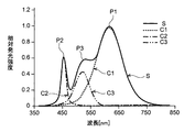
また、図6に示すように、本実施の形態において、LEDチップ21からの光の発光スペクトルS(図6の実線参照)は、中心波長が610nm以上630nm以下である第1のピークP1と、中心波長が440nm以上460nm以下である第2のピークP2と、中心波長が510nm以上530nm以下である第3のピークP3とを有している。すなわち、発光スペクトルSは、赤色波長域に存在する第1のピークP1と、青色波長域に存在する第2のピークP2と、緑色波長域に存在する第3のピークP3とを有している。なお、LEDチップ21からの光の発光スペクトルは、光源色の測定に用いられる分光放射照度計(例えばコニカミノルタ社製、CL−500A)を用いて、光源色と同様に測定することができる。
Further, as shown in FIG. 6, in the present embodiment, the emission spectrum S of the light from the LED chip 21 (see the solid line in FIG. 6) includes the first peak P1 having a center wavelength of 610 nm or more and 630 nm or less. It has a second peak P2 having a center wavelength of 440 nm or more and 460 nm or less, and a third peak P3 having a center wavelength of 510 nm or more and 530 nm or less. That is, the emission spectrum S has a first peak P1 existing in the red wavelength region, a second peak P2 existing in the blue wavelength region, and a third peak P3 existing in the green wavelength region. .. The emission spectrum of the light from the
また、この場合、第1のピークP1の中心波長における相対発光強度は、第2のピークP2の中心波長における相対発光強度よりも大きく、第3のピークP3の中心波長における相対発光強度は、第2のピークP2の中心波長における相対発光強度よりも小さくなっている。すなわち、本明細書中、LEDチップ21からの光の発光スペクトルSのピークのうち、相対発光強度が最も大きいピークを第1のピークP1と称し、相対発光強度が2番目に大きいピークを第2のピークP2と称し、相対発光強度が3番目に大きいピークを第3のピークP3と称している。なお、LEDチップ21からの光は、4つ以上のピークを含んでいてもよい。LEDチップ21からの光の発光スペクトルSが上述したような第1のピークP1、第2のピークP2および第3のピークP3を有していることにより、LEDチップ21からの光が白色になるとともに、LEDチップ21の光源色を電球色または温白色とすることができる。
Further, in this case, the relative emission intensity at the center wavelength of the first peak P1 is larger than the relative emission intensity at the center wavelength of the second peak P2, and the relative emission intensity at the center wavelength of the third peak P3 is the third. It is smaller than the relative emission intensity at the center wavelength of the peak P2 of 2. That is, in the present specification, among the peaks of the emission spectrum S of the light from the
ここで、上述した発光スペクトルSに基づいて、LEDチップ21からの光の成分を導き出すことができる。この場合、光の成分は、波形分離ソフト(例えば、「fityk」)を用いた解析によって導き出すことができる。この際、まず、波形分離ソフトを用いて、光の発光スペクトルSを読み込む。次に、波形分離ソフトにおいて、読み込んだ発光スペクトルSの各ピーク(例えば、第1のピークP1、第2のピークP2および第3のピークP3)を選択する。次に、Voigt(フォークト)関数を用いて、測定された光の発光スペクトルに対してフィッティングを実行する。これにより、光の各成分を導き出すことができる。この場合、フィッティング後の波形と発光スペクトルの波形とにおいて、波形の高さ方向における最小二乗誤差が1%以下になるまで、フィッティングを繰り返し、光の各成分を導き出してもよい。
Here, the component of light from the
図6に示すように、本実施の形態において、LEDチップ21からの光は、中心波長が610nm以上630nm以下であるとともに半値幅が90nm以上110nm以下である第1の成分C1(図6の破線参照)と、中心波長が440nm以上460nm以下であるとともに半値幅が10nm以上20nm以下である第2の成分C2(図6の一点鎖線参照)と、中心波長が510nm以上530nm以下であるとともに半値幅が50nm以上60nm以下である第3の成分C3(図6の二点鎖線参照)とを有している。また、この場合、第1の成分C1の中心波長における相対発光強度は、第2の成分C2の中心波長における相対発光強度よりも大きく、第3の成分C3の中心波長における相対発光強度は、第2の成分C2の中心波長における相対発光強度よりも小さくなっている。すなわち、本明細書中、LEDチップ21からの光のうち、相対発光強度が最も大きい成分を第1の成分C1と称し、相対発光強度が2番目に大きい成分を第2の成分C2と称し、相対発光強度が3番目に大きい成分を第3の成分C3と称している。なお、LEDチップ21からの光は、4つ以上の成分を含んでいてもよい。LEDチップ21からの光が上述したような第1の成分C1、第2の成分C2および第3の成分C3を有していることにより、LEDチップ21からの光が白色になるとともに、LEDチップ21の光源色を電球色または温白色とすることができる。
As shown in FIG. 6, in the present embodiment, the light from the
また、第2の成分C2の中心波長における相対発光強度は、第1の成分C1の中心波長における相対発光強度の0.5倍以上0.7倍以下であり、第3の成分C3の中心波長における相対発光強度は、第1の成分C1の中心波長における相対発光強度の0.3倍以上0.5倍以下である。これにより、LEDチップ21の光源色を電球色または温白色とすることができる。このように、LEDチップ21の光源色を、昼白色に比べて、光合成の量子効率が良いと考えられている電球色または温白色にすることができるため、植物体の成長を促すことができる。
Further, the relative emission intensity at the center wavelength of the second component C2 is 0.5 times or more and 0.7 times or less the relative emission intensity at the center wavelength of the first component C1, and the center wavelength of the third component C3. The relative emission intensity in the above is 0.3 times or more and 0.5 times or less the relative emission intensity at the center wavelength of the first component C1. As a result, the light source color of the
また、図7に示すように、本実施の形態において、LEDチップ21からの光の色度は、xy色度図において、(0.39,0.36)、(0.41,0.44)、(0.46,0.44)、(0.42,0.36)の4つの色度座標を結ぶ四角形の領域(図7の網掛け部分)内にある。この場合、LEDチップ21からの光が白色になるとともに、図7に示すように、LEDチップ21からの光の色温度が、約2,900K以上約3,600K以下程度となる。これにより、植物の育成を速め、植物の育成量を増加するとともに育成日数を短縮することができる。このため、植物育成工場90における植物の収量を向上させることができる。なお、LEDチップ21からの光の色度は、光源色の測定に用いられる分光放射照度計(例えばコニカミノルタ社製、CL−500A)を用いて、光源色と同様に測定することができる。
Further, as shown in FIG. 7, in the present embodiment, the chromaticity of the light from the
また、LEDチップ21としては、発光効率が高いものを選択することが好ましい。具体的には、LEDチップ21として、150lm/W以上の発光効率を有しているものを用いることが好ましく、180lm/W以上の発光効率を有しているものを用いることが更に好ましい。LEDチップ21の発光効率を150lm/W以上に高めることにより、LEDチップ21の実装数(密度)を下げ、LEDチップ21からのジュール熱による発熱を少なくすることができ、LEDチップ21からの熱による植物の育成のばらつきが発生しにくくなって収量の低下を抑制することができる。
Further, it is preferable to select an
LED照明シート20は、上述の通り、高い放熱性を発揮することができる金属配線部32に、LEDチップ21を直接実装するものである。これにより、LEDチップ21を高密度で配置した場合においても、LEDチップ21の点灯時に発生する過剰な熱を金属配線部32を通して速やかに拡散し、基板フィルム31を介してLED照明シート20の外部へ十分放熱することができ、LEDチップ21からの熱による植物の育成のばらつきが発生しにくくなって収量の低下を抑制することができる。
As described above, the
(光反射性絶縁保護膜)
図5に示すように、光反射性絶縁保護膜34は、LEDチップ21が設けられている領域及びその周辺領域を除く領域に形成される層である。この光反射性絶縁保護膜34は、十分な絶縁性を有することにより、フレキシブル配線基板30の耐マイグレーション特性を向上させる所謂レジスト層であり、かつLED照明シート20により作られる光環境の発光輝度の向上に寄与する光反射性を備えた光反射層である。
(Light reflective insulating protective film)
As shown in FIG. 5, the light-reflecting insulating
光反射性絶縁保護膜34は、ウレタン系樹脂等をベース樹脂とし、酸化チタン等の無機フィラーからなる白色顔料を更に含有する各種の樹脂組成物により形成することができる。光反射性絶縁保護膜34を形成するために用いる樹脂組成物のベース樹脂としては、ウレタン系樹脂の他、アクリル系ポリウレタン樹脂、ポリエステル系樹脂、フェノール系樹脂等を適宜用いることができる。光反射性絶縁保護膜34を形成する樹脂組成物のベース樹脂としては、透明保護膜35を形成する樹脂組成物と同一または同系の樹脂をベース樹脂とすることがより好ましい。透明保護膜35については、後述するように、アクリル系ポリウレタン樹脂を主たる材料樹脂として用いることが好ましい。これより、透明保護膜35を形成する樹脂組成物のベース樹脂がアクリル系ポリウレタン樹脂である場合には、光反射性絶縁保護膜34を形成するための樹脂組成物のベース樹脂はウレタン系樹脂またはアクリル系ポリウレタン樹脂とすることがより好ましい。
The light-reflecting insulating
光反射性絶縁保護膜34を形成する樹脂組成物に白色顔料として含有させる無機フィラーとしては、酸化チタンの他、アルミナ、硫酸バリウム、マグネシア、チッ化アルミニウム、チッ化ホウ素、チタン酸バリウム、カオリン、タルク、炭酸カルシウム、酸化亜鉛、シリカ、マイカ粉、粉末ガラス、粉末ニッケル及び粉末アルミニウムから選ばれる少なくとも1種を用いることができる。
Examples of the inorganic filler to be contained as a white pigment in the resin composition forming the light-reflecting insulating
光反射性絶縁保護膜34の厚さは、5μm以上50μm以下であって、より好ましくは、7μm以上20μm以下である。光反射性絶縁保護膜34の厚さが、5μm未満であると、特に金属配線部32のエッジ部分において、光反射性絶縁保護膜が薄くなり、この金属配線を被覆できずに露出する場合は絶縁性が維持できなくなるリスクが大きくなる。一方、取扱い及び搬送等の際の基板湾曲から光反射性絶縁保護膜34を保持する観点から、光反射性絶縁保護膜34の厚さは、50μm以下であることが好ましい。
The thickness of the light-reflecting insulating
また、光反射性絶縁保護膜34は、波長400nm以上780nm以下における光線反射率が、いずれも65%以上であることが好ましく、70%以上であることがより好ましく、80%以上であることが更に好ましい。LED照明シート20は、例えば、酸化チタンを、ウレタン系またはアクリル系ポリウレタンのベース樹脂100質量部に対して20質量部以上含有させることで、光反射性絶縁保護膜34の厚さを8μmとする場合における同層の上記光線反射率を75%以上とすることが可能である。
Further, the light-reflecting insulating
(透明保護膜)
透明保護膜35は、LEDチップ21を覆うように、LED照明シート20の最表面に形成されている。透明保護膜35は、防水性と透明性とを有する。透明保護膜35の防水性により、LED照明シート20を植物育成用光源として使用する場合の装置内部への水の侵入を防ぐことができる。LEDチップ21として、例えば150lm/W以上の発光効率を有するような、発光効率が高いものを選択した場合、LED照明シート20において、特定のLEDチップ21が破損した場合の影響が大きくなる。そのためLEDチップ21が可能な限り破損しにくいようにすることは、リスク管理の観点で重要である。
(Transparent protective film)
The transparent
透明保護膜35は、アクリル系ポリウレタン樹脂等をベース樹脂とする各種の樹脂組成物により形成することができる。透明保護膜35を形成するために用いる樹脂組成物のベース樹脂としては、アクリル系ポリウレタン樹脂の他、ウレタン系樹脂、ポリエステル系樹脂、フェノール系樹等を適宜用いることができる。透明保護膜35を形成する樹脂組成物のベース樹脂としては、光反射性絶縁保護膜34を形成する樹脂組成物と同一または同系の樹脂をベース樹脂とすることがより好ましい。好ましい具体的な組合せとして、光反射性絶縁保護膜34を形成する樹脂組成物のベース樹脂をウレタン系樹脂とし、透明保護膜35を形成する同樹脂をアクリル系ポリウレタン樹脂とする組合せを挙げることができる。
The transparent
透明保護膜35の厚さは、10μm以上40μm以下であり、好ましくは15μm以上30μm以下であり、より好ましくは20μm以上25μm以下である。透明保護膜35の厚さを上記範囲とすることにより、LED照明シート20の良好な可撓性や薄さ、軽量性、及び植物育成用途において求められる良好な光学特性を維持することができる。また、LED照明シート20に対して植物育成用途に求められる十分な防水性をもたらすことができる。
The thickness of the transparent
透明保護膜35によるLED照明シート20の耐水性としては、LED照明シート20に対して植物育成用の水を散布した際に、LEDチップ21の劣化を抑制することが可能となる程度であれば特に限定されない。このような耐水性としては、IEC(国際電気標準会議)によって定められている防水・防塵の保護規格でIPX4以上を示すことが好ましい。IPX4以上の防水性は、あらゆる方向からの水の飛沫によってLEDチップ21に対して有害な影響が及ぼされない程度である。具体的には、LED照明シート20の法線方向に対して±180°の全範囲に5分間、10L/分の水量で散水ノズルから散水した際、LEDチップ21に対して有害な影響が及ぼされない程度とされる。
The water resistance of the
(LED照明シートの製造方法)
次に、本実施の形態によるLED照明シート20の製造方法について、図8(a)−(h)を参照して説明する。
(Manufacturing method of LED lighting sheet)
Next, a method of manufacturing the
まず、基板フィルム31を準備する(図8(a))。次に、基板フィルム31の表面に、金属配線部32の材料となる銅箔等の金属箔32Aを積層する(図8(b))。金属箔32Aは、金属箔32Aを例えばウレタン系接着剤等の接着剤層33によって、基板フィルム31の表面に接着される。あるいは、金属箔32Aは、基板フィルム31の表面に電解メッキ方法や気相製膜法(スパッタリング、イオンプレーティング、電子ビーム蒸着、真空蒸着、化学蒸着等)により、直接形成しても良い。もしくは、金属箔32Aに基板フィルム31を直接溶着して形成しても良い。
First, the
次に、金属箔32Aの表面に、金属配線部32に要求される形状にパターニングされたエッチングマスク37を形成する(図8(c))。このエッチングマスク37は、金属配線部32となる金属箔32Aの配線パターンに対応する部分がエッチング液によって腐食しないように設けられる。エッチングマスク37を形成する方法は特に限定されず、例えば、フォトレジストまたはドライフィルムを、フォトマスクを通して感光させた後に現像することによって形成しても良く、インクジェットプリンター等の印刷技術により金属箔32Aの表面にエッチングマスクを形成してもよい。
Next, an
次に、エッチングマスク37に覆われていない箇所に位置する金属箔32Aを浸漬液により除去する(図8(d))。これにより、金属箔32Aのうち、金属配線部32となる箇所以外の部分が除去される。
Next, the
その後、アルカリ性の剥離液を使用して、エッチングマスク37を除去する。これにより、エッチングマスク37が金属配線部32の表面から除去される(図8(e))。
The
続いて、金属配線部32上に光反射性絶縁保護膜34を積層形成する(図8(f))。光反射性絶縁保護膜34の形成は、光反射性絶縁保護膜34を構成する材料樹脂組成物を均一に塗工できる塗工手段であれば特に限定されず、例えば、スクリーン印刷、オフセット印刷、ディップコータ、刷毛塗り等の方法を使用することができる。または、光感光性を有する絶縁保護膜材料を全面に塗工し、必要な箇所のみフォトマスクを通して感光させた後に現像することによって光反射性絶縁保護膜34を形成しても良い。
Subsequently, the light-reflecting insulating
次に、金属配線部32上にLEDチップ21、レギュレータ45及びコネクタ44A、44Bを実装する(図8(g))。なお、図8(g)および後述する図8(h)においては、図面を明瞭にするために、レギュレータ45等の図示を省略している。この場合、LEDチップ21は、金属配線部32にハンダ部36を介するハンダ加工によって接合される。このハンダ加工による接合は、リフロー方式、あるいは、レーザー方式によることができ、または導電性樹脂による接合でも良い。
Next, the
次いで、光反射性絶縁保護膜34、LEDチップ21、レギュレータ45及びコネクタ44A、44Bを覆うように透明保護膜35を形成する(図8(h))。この透明保護膜35は、透明樹脂組成物をスプレー処理により吹付けて形成する方法(以下、「スプレーコート法」という)、またはカーテンコート法により形成する方法により行うことが好ましい。スプレーコート法による透明保護膜35の形成は、例えば、アクリル系ポリウレタン樹脂を含むスプレーコート処理用の塗工液を、スプレー塗装機によってフレキシブル配線基板30上の所望の領域に噴霧して塗工膜を形成することにより行うことができる。カーテンコート法による透明保護膜35の形成は、例えば、アクリル系ポリウレタン樹脂を含むカーテンコート処理用の塗工液を、カーテン塗装機によってフレキシブル配線基板30上の所望の領域に滴下して塗工膜を形成することにより行うことができる。
Next, a transparent
なお、本実施の形態によるLED照明シート20は、上述した方法に限らず、従来公知のLEDチップ用のフレキシブル配線基板や、これにLEDチップを実装してなる各種のLEDモジュールを製造する公知の方法により製造することもできる。
The
(植物育成工場及び植物の育成棚)
図9は、本実施の形態によるLED照明シート20を用いた植物育成工場90の構成を模式的に示す図である。植物育成工場90は、建物91と、建物91の内部に配置された複数の植物の育成棚80を備えている。
(Plant growing factory and plant growing shelf)
FIG. 9 is a diagram schematically showing the configuration of a
図10に示すように、植物の育成棚80は、複数(4本)の支柱82と、支柱82に沿ってそれぞれ上下方向に間隔を空けて配置された複数の基板81とを有している。最上段の基板81を除く各基板81の上面には、植物PLを栽培するための培地領域が設けられている。最下段の基板81を除く各基板81の下面は、当該基板81の下方に位置する基板81に対して天井面を構成しており、LED照明シート20が並列に配置されている。この場合、制御部40はLED照明シート20から十分に離れた場所に配置される。このため、制御部40に近い位置にある植物PLと遠い位置にある植物PLとで、制御部40からの熱によって生育にばらつきが生じるおそれが少ない。また、基板81と、基板81の下面側に取り付けられたLED照明シート20とにより、植物の育成棚用の棚板83が構成される。あるいは、基板81と、基板81の下面側に取り付けられたLED照明モジュール10とにより、植物の育成棚用の棚板83が構成される。本実施の形態において、このような植物の育成棚用の棚板83(図10)、植物の育成棚80(図10)、及び植物の育成棚80を備えた植物育成工場90(図9)も提供する。
As shown in FIG. 10, the
本実施の形態によるLED照明シート20が可撓性と軽量性を有することにより、各基板81の下面へのLED照明シート20の取付けは、従来の直管型の照明装置等による取付けよりも容易に行うことができる。さらに、LED照明シート20が可撓性を有することにより、LED照明シート20を、様々なサイズや形状からなる天井面へ取り付けることができる。この結果、本実施の形態によるLED照明シート20は、様々な植物の育成棚80や植物育成工場90へ適用することができる。
Since the
また、LED照明シート20は、従来の直管型の照明装置と比較して薄型化されている。これにより、上下方向の基板81の間隔を狭めることができ、各植物の育成棚80に含まれる基板81の数を増やすことができる。この結果、単位面積あたりの植物PLの収穫量を増加することができる。
Further, the
なお、図11(a)−(b)に示すように、LED照明シート20は、基板81の下面だけでなく、基板81の側面側にも配置しても良い。この側面側のLED照明シート20は、上方に位置する基板81から、当該基板81の下方に位置する基板81に向けて垂下されている。この場合、図11(a)に示すように、LED照明シート20は、下方に位置する基板81まで達していても良い。あるいは、図11(b)に示すように、LED照明シート20は、下方に位置する基板81まで達することなく、上下の基板81間に位置する空間の上部側のみを覆うようにしても良い。このように、LED照明シート20を、基板81の側面側にもさらに配置することにより、照度が弱くなりやすい基板81の周縁における光量を補い、LED照明シート20の輝度を面内で均一にすることができる。この結果、植物の成長を面内で均一にすることができ、育成する植物の収量の向上を図ることができる。
As shown in FIGS. 11A to 11B, the
このように本実施の形態によれば、LEDチップ21の光源色が、JIS Z 9112に規定される光源色のうち、電球色または温白色である。これにより、植物の育成を速め、植物の育成量を増加するとともに育成日数を短縮することができる。すなわち、LEDチップ21の光源色が、昼白色に比べ、光合成の量子効率が良いと考えられている電球色または温白色であるため、植物体の成長を促すことができる。この結果、植物育成工場90における植物の収量を向上させることができる。
As described above, according to the present embodiment, the light source color of the
また、本実施の形態によれば、LEDチップ21の光源色が、JIS Z 9112に規定される光源色のうち、電球色である。これにより、植物育成工場90で作業する作業者の目が疲れにくくなり、作業効率を向上させることができる。
Further, according to the present embodiment, the light source color of the
また、本実施の形態によれば、LEDチップ21からの光の発光スペクトルSが、中心波長が610nm以上630nm以下である第1のピークP1と、中心波長が440nm以上460nm以下である第2のピークP2と、中心波長が510nm以上530nm以下である第3のピークP3とを有している。また、第1のピークP1の中心波長における相対発光強度は、第2のピークP2の中心波長における相対発光強度よりも大きく、第3のピークP3の中心波長における相対発光強度は、第2のピークP2の中心波長における相対発光強度よりも小さくなっている。これにより、LEDチップ21からの光が白色になるとともに、LEDチップ21の光源色を電球色または温白色とすることができる。このため、上述した効果を得ることができる。
Further, according to the present embodiment, the emission spectrum S of the light from the
また、本実施の形態によれば、LEDチップ21からの光は、中心波長が610nm以上630nm以下であるとともに半値幅が90nm以上110nm以下である第1の成分C1と、中心波長が440nm以上460nm以下であるとともに半値幅が10nm以上20nm以下である第2の成分C2と、中心波長が510nm以上530nm以下であるとともに半値幅が50nm以上60nm以下である第3の成分C3とを有している。また、第1の成分C1の中心波長における相対発光強度は、第2の成分C2の中心波長における相対発光強度よりも大きく、第3の成分C3の中心波長における相対発光強度は、第2の成分C2の中心波長における相対発光強度よりも小さくなっている。これにより、LEDチップ21からの光が白色になるとともに、LEDチップ21の光源色を電球色または温白色とすることができる。このため、上述した効果を得ることができる。
Further, according to the present embodiment, the light from the
また、本実施の形態によれば、第2の成分C2の中心波長における相対発光強度が、第1の成分C1の中心波長における相対発光強度の0.5倍以上0.7倍以下であり、第3の成分C3の中心波長における相対発光強度は、第1の成分C1の中心波長における相対発光強度の0.3倍以上0.5倍以下である。これにより、LEDチップ21の光源色を電球色または温白色とすることができる。このように、LEDチップ21の光源色を、昼白色に比べて、光合成の量子効率が良いと考えられている電球色または温白色にすることができるため、植物体の成長を促すことができる。
Further, according to the present embodiment, the relative emission intensity at the center wavelength of the second component C2 is 0.5 times or more and 0.7 times or less the relative emission intensity at the center wavelength of the first component C1. The relative emission intensity at the center wavelength of the third component C3 is 0.3 times or more and 0.5 times or less the relative emission intensity at the center wavelength of the first component C1. As a result, the light source color of the
また、本実施の形態によれば、LEDチップ21からの光の色度は、xy色度図において、(0.39,0.36)、(0.41,0.44)、(0.46,0.44)、(0.42,0.36)の4つの色度座標を結ぶ四角形の領域内にある。この場合、LEDチップ21からの光が白色になるとともに、LEDチップ21からの光の色温度が、約2,900K以上約3,600K以下程度となる。これにより、植物の育成を速め、植物の育成量を増加するとともに育成日数を短縮することができる。このため、植物育成工場90における植物の収量を向上させることができる。
Further, according to the present embodiment, the chromaticity of the light from the
また本実施の形態によれば、LEDチップ21は、10個以上直列に配置され、このLEDチップ21の列が4列以上並列に配置されている。これにより、LEDチップ21を面内で均一に配置するとともに、LEDチップ21の配列を並列化し、LEDチップ21が破損した際のリスクを分散することができる。
Further, according to the present embodiment, 10 or
また本実施の形態によれば、LEDチップ21は、透明保護膜35によって覆われているので、植物の育成時に飛散する水分からLEDチップ21を保護することができる。
Further, according to the present embodiment, since the
また本実施の形態によれば、LED照明シート20の最も厚い部分における厚みが5mm以下であるので、植物の育成棚80の上下の基板81間の距離を減らし、基板81の数を増やすことにより、単位面積あたりの植物の収量を増加することができる。
Further, according to the present embodiment, since the thickness of the thickest portion of the
また本実施の形態によれば、制御部40は、LED照明シート20に対して外付けで接続されるので、制御部40をLED照明シート20から離し、植物に制御部40からの熱の影響が及ばないようにすることができる。
Further, according to the present embodiment, since the
また本実施の形態によれば、制御部40からLED照明シート20に定電圧が印加されるので、LEDチップ21からの単位時間当たりの積算光量を増やし、植物の生育を促進することができる。
Further, according to the present embodiment, since a constant voltage is applied from the
また本実施の形態によれば、制御部40は、LEDチップ21の調光を制御可能となっているので、植物の生育段階に応じて、LEDチップ21からの光の強度を調整することができる。
Further, according to the present embodiment, since the
なお、上述した本実施の形態においては、LED照明装置が面状の光源シートである場合について説明したが、これに限られない。例えば、図示はしないが、LED照明装置は、直管型の照明装置であってもよい。 In the above-described embodiment, the case where the LED lighting device is a planar light source sheet has been described, but the present invention is not limited to this. For example, although not shown, the LED lighting device may be a straight tube type lighting device.
[実施例]
次に、本実施の形態における具体的実施例について説明する。
[Example]
Next, a specific example in the present embodiment will be described.
(LED照明シートの作成)
実施例1、2及び比較例のLED照明シートをそれぞれ以下の通り作製した。
(Creation of LED lighting sheet)
The LED lighting sheets of Examples 1 and 2 and Comparative Example were produced as follows.
(実施例1)
560mm×390mmサイズのフィルム基板(ポリエチレンナフタレート、厚さ50μm)の一方の表面に、金属配線部を形成するための銅箔(厚さ35μm)を積層し、その後、金属配線用の銅箔についてエッチング処理をして、全ての実施例及び比較例において同一パターンの金属配線部を構成した。そして、基板フィルム及び金属配線部上に、ウレタン系樹脂をベース樹脂とし、このベース樹脂に対して20質量%の割合で酸化チタンを添加してなる絶縁性インキを用いてスクリーン印刷により厚さ10μmの光反射性絶縁保護膜を形成した。次に、金属配線部に、複数のLEDチップ(「NFSW757G−V2」(日亜化学工業社製))を、X方向に40mmピッチ、Y方向に35mmピッチで、14個の列を10列、ハンダ加工により実装した。なお、このLEDチップは、上面発光タイプの発光素子であり、3.0mm(長さ)×3.0mm(幅)×0.65mm(高さ)のサイズの直方体の外形からなるものである。また、このLEDチップの光源色はそれぞれ電球色であり、それぞれの色温度が3000Kのものである。更に、上記の絶縁性保護膜及びLEDチップを被覆する透明保護膜を、スプレーコート法により形成した。以上の通り作製したLED照明シートを実施例1のLED照明シートとした。
(Example 1)
A copper foil (
(実施例2)
LEDチップとして、光源色が温白色であり、色温度が3500Kのもの(「NFSW757G−V2」(日亜化学工業社製))を用いたこと、以外は、実施例1と同様に作製したLED照明シートを、実施例2のLED照明シートとした。
(Example 2)
As the LED chip, an LED manufactured in the same manner as in Example 1 except that the light source color is warm white and the color temperature is 3500K (“NFSW757G-V2” (manufactured by Nichia Corporation)) is used. The lighting sheet was the LED lighting sheet of Example 2.
(比較例)
LEDチップとして、光源色が昼白色であり、色温度が5000Kのもの(「NFSW757G−V2」(日亜化学工業社製))を用いたこと、以外は、実施例1と同様に作製したLED照明シートを、比較例のLED照明シートとした。
(Comparison example)
As the LED chip, an LED manufactured in the same manner as in Example 1 except that a light source color of neutral white and a color temperature of 5000 K (“NFSW757G-V2” (manufactured by Nichia Corporation)) was used. The lighting sheet was an LED lighting sheet of a comparative example.
実施例1、2及び比較例のLED照明シートに用いたLEDチップについて、光学特性、具体的には、光の発光スペクトルを測定した。光の発光スペクトルは、分光放射照度計(コニカミノルタ社製、CL−500A)により測定した。測定された発光スペクトルは、それぞれ第1のピーク、第2のピークおよび第3のピークを有しており、第1のピーク、第2のピークおよび第3のピークの中心波長をそれぞれ測定した。 The optical characteristics of the LED chips used in the LED lighting sheets of Examples 1 and 2 and Comparative Examples, specifically, the emission spectrum of light were measured. The emission spectrum of light was measured by a spectroscopic irradiance meter (CL-500A, manufactured by Konica Minolta). The measured emission spectrum had a first peak, a second peak and a third peak, respectively, and the center wavelengths of the first peak, the second peak and the third peak were measured, respectively.
また、実施例1、2及び比較例のLED照明シートに用いたLEDチップについて、測定した発光スペクトルから、波形分離ソフト「fityk」を用いて、光の成分を導き出した。この際、まず、測定された光の発光スペクトルを読み込み、第1のピーク、第2のピークおよび第3のピークを選択した。次に、Voigt(フォークト)関数を用いて、測定された光の発光スペクトルに対してフィッティングを実行した。そして、フィッティング後の波形と発光スペクトルの波形とにおいて、波形の高さ方向における誤差が1%以下になるまで、フィッティングを繰り返し、光の第1の成分、第2の成分および第3の成分を導き出した。そして、導き出された第1の成分、第2の成分および第3の成分の中心波長および半値幅をそれぞれ測定した。 Further, with respect to the LED chips used for the LED lighting sheets of Examples 1 and 2 and Comparative Example, the light component was derived from the measured emission spectrum by using the waveform separation software "fityk". At this time, first, the emission spectrum of the measured light was read, and the first peak, the second peak, and the third peak were selected. The Voigt function was then used to perform fittings on the measured emission spectrum of the light. Then, in the waveform after fitting and the waveform of the emission spectrum, fitting is repeated until the error in the height direction of the waveform becomes 1% or less, and the first component, the second component, and the third component of light are removed. Derived. Then, the center wavelength and the full width at half maximum of the derived first component, second component, and third component were measured, respectively.
続いて、実施例1、2及び比較例のLED照明シートをそれぞれ植物の育成棚に取り付け、植物(ベビースピナッチ)を実際に栽培した。その後、生育した植物の生体重(g/m2)を測定した。この生体重の測定は、栽培終了後の地上部生体重を栽培パネル毎に計測し平米あたりの重量に計算することで算出した。また、栽培日数あたりの生体重である日産生体重(g/m2/day)を算出した。以上の評価結果を表1に示す。 Subsequently, the LED lighting sheets of Examples 1 and 2 and Comparative Example were attached to the growing shelves of the plants, respectively, and the plants (baby spinach) were actually cultivated. Then, the living body weight (g / m 2 ) of the grown plant was measured. This biological weight was calculated by measuring the above-ground biological weight after cultivation for each cultivation panel and calculating the weight per square meter. In addition, the daily body weight (g / m 2 / day), which is the living body weight per cultivation day, was calculated. The above evaluation results are shown in Table 1.

上記表1に示すように、実施例1、2のLED照明シートを用いた場合、比較例のLED照明シートを用いた場合よりも、植物の生体重を増加させることができた。具体的には、実施例1のLED照明シート(LEDチップの光源色が電球色)を用いた場合、比較例のLED照明シート(LEDチップの光源色が昼白色)を用いた場合と比較して、日産生体重(g/m2/day)を9%増加させることができた。また、実施例2のLED照明シート(LEDチップの光源色が温白色)を用いた場合、比較例のLED照明シート(LEDチップの光源色が昼白色)を用いた場合と比較して、日産生体重(g/m2/day)を6%増加させることができた。このように、実施例1、2のLED照明シートを用いた場合、LEDチップの光源色を電球色または温白色にしたことにより、植物の生産性を向上させることができた。 As shown in Table 1 above, when the LED lighting sheets of Examples 1 and 2 were used, the biological weight of the plant could be increased as compared with the case of using the LED lighting sheets of the comparative example. Specifically, when the LED lighting sheet of Example 1 (the light source color of the LED chip is the light bulb color) is used, it is compared with the case where the LED lighting sheet of the comparative example (the light source color of the LED chip is neutral white) is used. As a result, the daily production weight (g / m 2 / day) could be increased by 9%. Further, when the LED lighting sheet of Example 2 (the light source color of the LED chip is warm white) is used, compared with the case where the LED lighting sheet of the comparative example (the light source color of the LED chip is neutral white) is used, Nissan The raw weight (g / m 2 / day) could be increased by 6%. As described above, when the LED lighting sheets of Examples 1 and 2 were used, the productivity of the plant could be improved by changing the light source color of the LED chip to a light bulb color or a warm white color.
上記実施の形態および変形例に開示されている複数の構成要素を必要に応じて適宜組合せることも可能である。あるいは、上記実施の形態および変形例に示される全構成要素から幾つかの構成要素を削除してもよい。 It is also possible to appropriately combine a plurality of components disclosed in the above-described embodiments and modifications as necessary. Alternatively, some components may be removed from all the components shown in the above embodiments and modifications.
10 LED照明モジュール
20 LED照明シート
21 LEDチップ
22 金属配線部
30 フレキシブル配線基板
31 基板フィルム
32 金属配線部
33 接着剤層
34 光反射性絶縁保護膜
35 透明保護膜
36 ハンダ部
40 制御部
41 電力入力部
42 AC/DCコンバーター
43 PWM制御部
44A 第1コネクタ
44B 第2コネクタ
45 レギュレータ
46 電力供給ライン
80 植物の育成棚
81 基板
82 支柱
83 植物の育成棚用の棚板
90 植物育成工場
91 建物
10
Claims (14)
前記LEDチップからの光は、中心波長が610nm以上630nm以下である第1の成分と、
中心波長が440nm以上460nm以下である第2の成分と、
中心波長が510nm以上530nm以下である第3の成分とを有し、
前記第3の成分の中心波長における相対発光強度は、前記第1の成分の中心波長における相対発光強度の0.3倍以上である、動植物育成用のLED照明装置。 An LED lighting device for growing animals and plants in which multiple LED chips are arranged.
The light from the LED chip includes a first component having a center wavelength of 610 nm or more and 630 nm or less.
A second component having a center wavelength of 440 nm or more and 460 nm or less,
It has a third component having a central wavelength of 510 nm or more and 530 nm or less.
An LED lighting device for growing animals and plants, wherein the relative emission intensity at the center wavelength of the third component is 0.3 times or more the relative emission intensity at the center wavelength of the first component.
前記第2の成分は、半値幅が10nm以上20nm以下であり、
前記第3の成分は、半値幅が50nm以上60nm以下である、請求項1記載の動植物育成用のLED照明装置。 The first component has a half width of 90 nm or more and 110 nm or less.
The second component has a half width of 10 nm or more and 20 nm or less.
The LED lighting device for growing animals and plants according to claim 1, wherein the third component has a half width of 50 nm or more and 60 nm or less.
前記第3の成分の中心波長における相対発光強度は、前記第2の成分の中心波長における相対発光強度よりも小さい、請求項1又は2記載の動植物育成用のLED照明装置。 The relative emission intensity of the first component at the center wavelength is larger than the relative emission intensity of the second component at the center wavelength.
The LED lighting device for growing animals and plants according to claim 1 or 2, wherein the relative emission intensity at the center wavelength of the third component is smaller than the relative emission intensity at the center wavelength of the second component.
請求項1乃至7のいずれか一項記載の動植物育成用のLED照明装置と、
前記動植物育成用のLED照明装置に電気的に接続された制御部とを備え、
前記制御部は、前記動植物育成用のLED照明装置に対して外付けで接続される、動植物育成用のLED照明モジュール。 An LED lighting module for growing animals and plants
The LED lighting device for growing animals and plants according to any one of claims 1 to 7.
It is provided with a control unit electrically connected to the LED lighting device for growing animals and plants.
The control unit is an LED lighting module for growing animals and plants that is externally connected to the LED lighting device for growing animals and plants.
基板と、
前記基板に取り付けられた、請求項1乃至7のいずれか一項記載の動植物育成用のLED照明装置または請求項8乃至10のいずれか一項記載の動植物育成用のLED照明モジュールとを備えた、動植物の育成棚用の棚板。 It is a shelf board for growing animals and plants,
With the board
The LED lighting device for growing animals and plants according to any one of claims 1 to 7 or the LED lighting module for growing animals and plants according to any one of claims 8 to 10 is provided on the substrate. , Shelf board for growing plants and animals.
棚板を備え、
前記棚板は、基板の下面側に取り付けられた、請求項1乃至7のいずれか一項記載の動植物育成用のLED照明装置または請求項8乃至10のいずれか一項記載の動植物育成用のLED照明モジュールとを備えた、動植物の育成棚。 It is a breeding shelf for animals and plants.
Equipped with shelves
The LED lighting device for growing animals and plants according to any one of claims 1 to 7 or the LED lighting device for growing animals and plants according to any one of claims 8 to 10 attached to the lower surface side of the substrate. An animal and plant growing shelf equipped with an LED lighting module.
前記建物の内部に配置された、請求項12又は13記載の動植物の育成棚とを備えた、動植物育成工場。 Building and
An animal and plant growing factory provided with the animal and plant growing shelves according to claim 12 or 13, which is arranged inside the building.
Priority Applications (1)
| Application Number | Priority Date | Filing Date | Title |
|---|---|---|---|
| JP2020174214A JP2021022572A (en) | 2020-10-15 | 2020-10-15 | Led lighting device for animal/plant growth, led lighting module for animal/plant growth, shelf board for animal/plant growth shelf, animal/plant growth shelf, and animal/plant growth factory |
Applications Claiming Priority (1)
| Application Number | Priority Date | Filing Date | Title |
|---|---|---|---|
| JP2020174214A JP2021022572A (en) | 2020-10-15 | 2020-10-15 | Led lighting device for animal/plant growth, led lighting module for animal/plant growth, shelf board for animal/plant growth shelf, animal/plant growth shelf, and animal/plant growth factory |
Related Parent Applications (1)
| Application Number | Title | Priority Date | Filing Date |
|---|---|---|---|
| JP2019019043A Division JP6780715B2 (en) | 2019-01-24 | 2019-02-05 | LED lighting device for growing animals and plants, LED lighting module for growing animals and plants, shelf board for growing shelves for animals and plants, growing shelves for animals and plants, and plant for growing animals and plants. |
Publications (2)
| Publication Number | Publication Date |
|---|---|
| JP2021022572A true JP2021022572A (en) | 2021-02-18 |
| JP2021022572A5 JP2021022572A5 (en) | 2021-04-01 |
Family
ID=74574371
Family Applications (1)
| Application Number | Title | Priority Date | Filing Date |
|---|---|---|---|
| JP2020174214A Pending JP2021022572A (en) | 2020-10-15 | 2020-10-15 | Led lighting device for animal/plant growth, led lighting module for animal/plant growth, shelf board for animal/plant growth shelf, animal/plant growth shelf, and animal/plant growth factory |
Country Status (1)
| Country | Link |
|---|---|
| JP (1) | JP2021022572A (en) |
Cited By (1)
| Publication number | Priority date | Publication date | Assignee | Title |
|---|---|---|---|---|
| KR102696760B1 (en) * | 2023-12-01 | 2024-08-19 | 백장현 | LED lighting device |
Citations (20)
| Publication number | Priority date | Publication date | Assignee | Title |
|---|---|---|---|---|
| JP2011155948A (en) * | 2010-02-03 | 2011-08-18 | Seiwa Electric Mfg Co Ltd | Light-emitting device for raising plant |
| JP4918957B2 (en) * | 2001-09-28 | 2012-04-18 | 岩崎電気株式会社 | Metal halide lamp for plant growth and lighting device for plant growth |
| JP4971623B2 (en) * | 2005-11-04 | 2012-07-11 | コーア株式会社 | Manufacturing method of LED light source device |
| JP3177205U (en) * | 2012-05-11 | 2012-07-26 | 株式会社ボルクスジャパン | Lighting equipment for aquarium |
| JP2012239417A (en) * | 2011-05-19 | 2012-12-10 | Ushio Inc | Light source apparatus for raising plant |
| JP3180774U (en) * | 2012-10-24 | 2013-01-10 | 昭和電工株式会社 | LED lamp for plant cultivation and LED lamp system for plant cultivation |
| JP2013153691A (en) * | 2012-01-31 | 2013-08-15 | Agri Wave Co Ltd | Plant cultivation system |
| JP5448043B2 (en) * | 2009-03-24 | 2014-03-19 | 国立大学法人山口大学 | Method for enhancing nutritional components of plants |
| JP5503760B1 (en) * | 2013-02-06 | 2014-05-28 | 三菱化工機株式会社 | LIGHT SOURCE DEVICE, LIGHTING DEVICE EQUIPPED WITH THE SAME, AND METHOD FOR MANUFACTURING LIGHT SOURCE DEVICE |
| JP2016072524A (en) * | 2014-09-30 | 2016-05-09 | 日亜化学工業株式会社 | Light emitting device and manufacturing method of the same |
| JP2016072189A (en) * | 2014-10-01 | 2016-05-09 | 久豊技研株式会社 | Light source device for illumination |
| JP2016202108A (en) * | 2015-04-24 | 2016-12-08 | スタンレー電気株式会社 | Cultivation method of phalaenopsis and light source equipment for use in it |
| JP2017091718A (en) * | 2015-11-06 | 2017-05-25 | 株式会社nittoh | Lighting module |
| JP2017127273A (en) * | 2016-01-21 | 2017-07-27 | 株式会社東芝 | Illuminator and cultivation apparatus |
| JP2018019667A (en) * | 2016-08-05 | 2018-02-08 | パナソニックIpマネジメント株式会社 | Lighting system, lighting control method and plant cultivation container |
| JP6282328B2 (en) * | 2016-09-26 | 2018-02-21 | パイオニア株式会社 | Light emitting device |
| JP2018033356A (en) * | 2016-08-31 | 2018-03-08 | 大日本印刷株式会社 | Plant cultivation apparatus and reflection sheet |
| JP6331248B2 (en) * | 2012-01-16 | 2018-05-30 | パナソニックIpマネジメント株式会社 | Plant growing device |
| US20180206411A1 (en) * | 2015-10-14 | 2018-07-26 | Starlight Led Inc. | Led flip chip plant grow light |
| JP2020126786A (en) * | 2019-02-05 | 2020-08-20 | 大日本印刷株式会社 | Led illumination device for animal and plant cultivation, led illumination module for animal and plant cultivation, shelf plate for cultivation shelf for animal and plant, cultivation shelf for animal and plant, and animal and plant cultivation factory |
-
2020
- 2020-10-15 JP JP2020174214A patent/JP2021022572A/en active Pending
Patent Citations (20)
| Publication number | Priority date | Publication date | Assignee | Title |
|---|---|---|---|---|
| JP4918957B2 (en) * | 2001-09-28 | 2012-04-18 | 岩崎電気株式会社 | Metal halide lamp for plant growth and lighting device for plant growth |
| JP4971623B2 (en) * | 2005-11-04 | 2012-07-11 | コーア株式会社 | Manufacturing method of LED light source device |
| JP5448043B2 (en) * | 2009-03-24 | 2014-03-19 | 国立大学法人山口大学 | Method for enhancing nutritional components of plants |
| JP2011155948A (en) * | 2010-02-03 | 2011-08-18 | Seiwa Electric Mfg Co Ltd | Light-emitting device for raising plant |
| JP2012239417A (en) * | 2011-05-19 | 2012-12-10 | Ushio Inc | Light source apparatus for raising plant |
| JP6331248B2 (en) * | 2012-01-16 | 2018-05-30 | パナソニックIpマネジメント株式会社 | Plant growing device |
| JP2013153691A (en) * | 2012-01-31 | 2013-08-15 | Agri Wave Co Ltd | Plant cultivation system |
| JP3177205U (en) * | 2012-05-11 | 2012-07-26 | 株式会社ボルクスジャパン | Lighting equipment for aquarium |
| JP3180774U (en) * | 2012-10-24 | 2013-01-10 | 昭和電工株式会社 | LED lamp for plant cultivation and LED lamp system for plant cultivation |
| JP5503760B1 (en) * | 2013-02-06 | 2014-05-28 | 三菱化工機株式会社 | LIGHT SOURCE DEVICE, LIGHTING DEVICE EQUIPPED WITH THE SAME, AND METHOD FOR MANUFACTURING LIGHT SOURCE DEVICE |
| JP2016072524A (en) * | 2014-09-30 | 2016-05-09 | 日亜化学工業株式会社 | Light emitting device and manufacturing method of the same |
| JP2016072189A (en) * | 2014-10-01 | 2016-05-09 | 久豊技研株式会社 | Light source device for illumination |
| JP2016202108A (en) * | 2015-04-24 | 2016-12-08 | スタンレー電気株式会社 | Cultivation method of phalaenopsis and light source equipment for use in it |
| US20180206411A1 (en) * | 2015-10-14 | 2018-07-26 | Starlight Led Inc. | Led flip chip plant grow light |
| JP2017091718A (en) * | 2015-11-06 | 2017-05-25 | 株式会社nittoh | Lighting module |
| JP2017127273A (en) * | 2016-01-21 | 2017-07-27 | 株式会社東芝 | Illuminator and cultivation apparatus |
| JP2018019667A (en) * | 2016-08-05 | 2018-02-08 | パナソニックIpマネジメント株式会社 | Lighting system, lighting control method and plant cultivation container |
| JP2018033356A (en) * | 2016-08-31 | 2018-03-08 | 大日本印刷株式会社 | Plant cultivation apparatus and reflection sheet |
| JP6282328B2 (en) * | 2016-09-26 | 2018-02-21 | パイオニア株式会社 | Light emitting device |
| JP2020126786A (en) * | 2019-02-05 | 2020-08-20 | 大日本印刷株式会社 | Led illumination device for animal and plant cultivation, led illumination module for animal and plant cultivation, shelf plate for cultivation shelf for animal and plant, cultivation shelf for animal and plant, and animal and plant cultivation factory |
Cited By (1)
| Publication number | Priority date | Publication date | Assignee | Title |
|---|---|---|---|---|
| KR102696760B1 (en) * | 2023-12-01 | 2024-08-19 | 백장현 | LED lighting device |
Similar Documents
| Publication | Publication Date | Title |
|---|---|---|
| WO2020153448A1 (en) | Led illumination sheet for animal and plant cultivation, led illumination module for animal and plant cultivation, shelf plate for cultivation shelf for animals and plants, cultivation shelf for animals and plants, animal and plant cultivation factory, and led illumination device for animal and plant cultivation | |
| JP7051725B2 (en) | LED lighting sheet for growing animals and plants, LED lighting module for growing animals and plants, shelf board for growing shelves for animals and plants, shelf for growing animals and plants, and plant for growing animals and plants. | |
| JP6780715B2 (en) | LED lighting device for growing animals and plants, LED lighting module for growing animals and plants, shelf board for growing shelves for animals and plants, growing shelves for animals and plants, and plant for growing animals and plants. | |
| JP7528173B2 (en) | Plant cultivation facility and plant cultivation method | |
| JP6969657B2 (en) | LED lighting sheet for growing animals and plants, LED lighting module for growing animals and plants, shelf board for growing shelves for animals and plants, shelf for growing animals and plants, and plant for growing animals and plants. | |
| JP6953461B2 (en) | LED lighting sheet for growing animals and plants, LED lighting module for growing animals and plants, shelf board for growing shelves for animals and plants, growing shelves for animals and plants, and plant for growing animals and plants. | |
| JP2021022572A (en) | Led lighting device for animal/plant growth, led lighting module for animal/plant growth, shelf board for animal/plant growth shelf, animal/plant growth shelf, and animal/plant growth factory | |
| JP7118904B2 (en) | Animal and plant growing LED lighting sheet, animal and plant growing LED lighting module, animal and plant growing shelf plate, animal and plant growing shelf, and animal and plant growing factory | |
| JP7535252B2 (en) | Plant and animal cultivation equipment | |
| JP7465459B2 (en) | LED lighting module for cultivating animals and plants, cultivating shelf for animals and plants, and cultivating factory for animals and plants | |
| JP7051732B2 (en) | LED lighting modules for growing animals and plants, shelves for growing animals and plants, and plants and animals growing factories | |
| JP7385832B2 (en) | LED lighting sheets for growing animals and plants, LED lighting modules for growing animals and plants, shelves for growing shelves for animals and plants, shelves for growing animals and plants, and plants for growing animals and plants | |
| JP2022021922A (en) | Led illumination module for growing plants and animals, shelf for growing plants and animals and factory for growing plants and animals | |
| JP7501197B2 (en) | LED lighting sheet for cultivating animals and plants, LED lighting module for cultivating animals and plants, shelf board for cultivating shelves for animals and plants, cultivating shelves for animals and plants, and plant and animal cultivating factory | |
| JP7404769B2 (en) | LED lighting sheet assembly for animal and plant growing shelves, animal and plant growing shelves, and animal and plant growing factories | |
| JP7340166B2 (en) | LED lighting sheets for growing animals and plants, LED lighting modules for growing animals and plants, shelves for growing shelves for animals and plants, shelves for growing animals and plants, and plants for growing animals and plants | |
| TW202426816A (en) | LED lighting sheets for animal and plant breeding, LED lighting modules for animal and plant breeding, shed boards for animal and plant breeding, animal and plant breeding sheds and animal and plant breeding factories |
Legal Events
| Date | Code | Title | Description |
|---|---|---|---|
| A521 | Request for written amendment filed |
Free format text: JAPANESE INTERMEDIATE CODE: A523 Effective date: 20210204 |
|
| A621 | Written request for application examination |
Free format text: JAPANESE INTERMEDIATE CODE: A621 Effective date: 20210204 |
|
| A871 | Explanation of circumstances concerning accelerated examination |
Free format text: JAPANESE INTERMEDIATE CODE: A871 Effective date: 20210204 |
|
| A975 | Report on accelerated examination |
Free format text: JAPANESE INTERMEDIATE CODE: A971005 Effective date: 20210205 |
|
| A131 | Notification of reasons for refusal |
Free format text: JAPANESE INTERMEDIATE CODE: A131 Effective date: 20210219 |
|
| A521 | Request for written amendment filed |
Free format text: JAPANESE INTERMEDIATE CODE: A523 Effective date: 20210319 |
|
| A02 | Decision of refusal |
Free format text: JAPANESE INTERMEDIATE CODE: A02 Effective date: 20210409 |