JP6953461B2 - LED lighting sheet for growing animals and plants, LED lighting module for growing animals and plants, shelf board for growing shelves for animals and plants, growing shelves for animals and plants, and plant for growing animals and plants. - Google Patents
LED lighting sheet for growing animals and plants, LED lighting module for growing animals and plants, shelf board for growing shelves for animals and plants, growing shelves for animals and plants, and plant for growing animals and plants. Download PDFInfo
- Publication number
- JP6953461B2 JP6953461B2 JP2019017453A JP2019017453A JP6953461B2 JP 6953461 B2 JP6953461 B2 JP 6953461B2 JP 2019017453 A JP2019017453 A JP 2019017453A JP 2019017453 A JP2019017453 A JP 2019017453A JP 6953461 B2 JP6953461 B2 JP 6953461B2
- Authority
- JP
- Japan
- Prior art keywords
- plants
- led lighting
- growing
- animals
- led
- Prior art date
- Legal status (The legal status is an assumption and is not a legal conclusion. Google has not performed a legal analysis and makes no representation as to the accuracy of the status listed.)
- Active
Links
- 241001465754 Metazoa Species 0.000 title claims description 114
- 229910052751 metal Inorganic materials 0.000 claims description 76
- 239000002184 metal Substances 0.000 claims description 76
- 239000000758 substrate Substances 0.000 claims description 66
- 230000001681 protective effect Effects 0.000 claims description 63
- 230000004907 flux Effects 0.000 claims description 24
- 230000000243 photosynthetic effect Effects 0.000 claims description 17
- 239000012463 white pigment Substances 0.000 claims description 4
- 238000009395 breeding Methods 0.000 claims 1
- 230000001488 breeding effect Effects 0.000 claims 1
- 241000196324 Embryophyta Species 0.000 description 206
- 229920005989 resin Polymers 0.000 description 33
- 239000011347 resin Substances 0.000 description 33
- 230000012010 growth Effects 0.000 description 26
- 230000000052 comparative effect Effects 0.000 description 21
- 238000000034 method Methods 0.000 description 16
- 239000011342 resin composition Substances 0.000 description 15
- 230000008635 plant growth Effects 0.000 description 13
- JOYRKODLDBILNP-UHFFFAOYSA-N Ethyl urethane Chemical compound CCOC(N)=O JOYRKODLDBILNP-UHFFFAOYSA-N 0.000 description 12
- NIXOWILDQLNWCW-UHFFFAOYSA-N acrylic acid group Chemical group C(C=C)(=O)O NIXOWILDQLNWCW-UHFFFAOYSA-N 0.000 description 11
- 239000011888 foil Substances 0.000 description 11
- 230000007423 decrease Effects 0.000 description 10
- 238000005530 etching Methods 0.000 description 9
- 239000000463 material Substances 0.000 description 9
- 230000002093 peripheral effect Effects 0.000 description 9
- 239000012790 adhesive layer Substances 0.000 description 7
- 238000005507 spraying Methods 0.000 description 7
- 239000000853 adhesive Substances 0.000 description 6
- 230000001070 adhesive effect Effects 0.000 description 6
- 239000011248 coating agent Substances 0.000 description 6
- 238000000576 coating method Methods 0.000 description 6
- 230000001678 irradiating effect Effects 0.000 description 6
- 239000010410 layer Substances 0.000 description 6
- 238000004519 manufacturing process Methods 0.000 description 6
- 229910000679 solder Inorganic materials 0.000 description 6
- XLYOFNOQVPJJNP-UHFFFAOYSA-N water Substances O XLYOFNOQVPJJNP-UHFFFAOYSA-N 0.000 description 6
- RYGMFSIKBFXOCR-UHFFFAOYSA-N Copper Chemical compound [Cu] RYGMFSIKBFXOCR-UHFFFAOYSA-N 0.000 description 5
- 238000005476 soldering Methods 0.000 description 5
- 229920002803 thermoplastic polyurethane Polymers 0.000 description 5
- GWEVSGVZZGPLCZ-UHFFFAOYSA-N Titan oxide Chemical compound O=[Ti]=O GWEVSGVZZGPLCZ-UHFFFAOYSA-N 0.000 description 4
- 239000011889 copper foil Substances 0.000 description 4
- 238000007766 curtain coating Methods 0.000 description 4
- 230000017525 heat dissipation Effects 0.000 description 4
- OGIDPMRJRNCKJF-UHFFFAOYSA-N titanium oxide Inorganic materials [Ti]=O OGIDPMRJRNCKJF-UHFFFAOYSA-N 0.000 description 4
- 229910052782 aluminium Inorganic materials 0.000 description 3
- XAGFODPZIPBFFR-UHFFFAOYSA-N aluminium Chemical compound [Al] XAGFODPZIPBFFR-UHFFFAOYSA-N 0.000 description 3
- 230000008901 benefit Effects 0.000 description 3
- 230000006866 deterioration Effects 0.000 description 3
- 238000010586 diagram Methods 0.000 description 3
- 206010016165 failure to thrive Diseases 0.000 description 3
- 239000011256 inorganic filler Substances 0.000 description 3
- 229910003475 inorganic filler Inorganic materials 0.000 description 3
- 238000009434 installation Methods 0.000 description 3
- 239000007788 liquid Substances 0.000 description 3
- 239000011159 matrix material Substances 0.000 description 3
- 230000005012 migration Effects 0.000 description 3
- 238000013508 migration Methods 0.000 description 3
- 239000011112 polyethylene naphthalate Substances 0.000 description 3
- VTYYLEPIZMXCLO-UHFFFAOYSA-L Calcium carbonate Chemical compound [Ca+2].[O-]C([O-])=O VTYYLEPIZMXCLO-UHFFFAOYSA-L 0.000 description 2
- CPLXHLVBOLITMK-UHFFFAOYSA-N Magnesium oxide Chemical compound [Mg]=O CPLXHLVBOLITMK-UHFFFAOYSA-N 0.000 description 2
- PXHVJJICTQNCMI-UHFFFAOYSA-N Nickel Chemical compound [Ni] PXHVJJICTQNCMI-UHFFFAOYSA-N 0.000 description 2
- ISWSIDIOOBJBQZ-UHFFFAOYSA-N Phenol Chemical compound OC1=CC=CC=C1 ISWSIDIOOBJBQZ-UHFFFAOYSA-N 0.000 description 2
- VYPSYNLAJGMNEJ-UHFFFAOYSA-N Silicium dioxide Chemical compound O=[Si]=O VYPSYNLAJGMNEJ-UHFFFAOYSA-N 0.000 description 2
- XLOMVQKBTHCTTD-UHFFFAOYSA-N Zinc monoxide Chemical compound [Zn]=O XLOMVQKBTHCTTD-UHFFFAOYSA-N 0.000 description 2
- 238000013459 approach Methods 0.000 description 2
- TZCXTZWJZNENPQ-UHFFFAOYSA-L barium sulfate Chemical compound [Ba+2].[O-]S([O-])(=O)=O TZCXTZWJZNENPQ-UHFFFAOYSA-L 0.000 description 2
- 230000037396 body weight Effects 0.000 description 2
- 230000003247 decreasing effect Effects 0.000 description 2
- 230000003111 delayed effect Effects 0.000 description 2
- 230000000694 effects Effects 0.000 description 2
- 238000011156 evaluation Methods 0.000 description 2
- 208000037824 growth disorder Diseases 0.000 description 2
- 230000009931 harmful effect Effects 0.000 description 2
- 238000009413 insulation Methods 0.000 description 2
- 238000012986 modification Methods 0.000 description 2
- 230000004048 modification Effects 0.000 description 2
- 229920001225 polyester resin Polymers 0.000 description 2
- -1 polyethylene terephthalate Polymers 0.000 description 2
- 229920000139 polyethylene terephthalate Polymers 0.000 description 2
- 239000005020 polyethylene terephthalate Substances 0.000 description 2
- 229920001721 polyimide Polymers 0.000 description 2
- 239000009719 polyimide resin Substances 0.000 description 2
- 229920005749 polyurethane resin Polymers 0.000 description 2
- 238000012545 processing Methods 0.000 description 2
- 238000007650 screen-printing Methods 0.000 description 2
- 239000004065 semiconductor Substances 0.000 description 2
- 238000007740 vapor deposition Methods 0.000 description 2
- RNFJDJUURJAICM-UHFFFAOYSA-N 2,2,4,4,6,6-hexaphenoxy-1,3,5-triaza-2$l^{5},4$l^{5},6$l^{5}-triphosphacyclohexa-1,3,5-triene Chemical compound N=1P(OC=2C=CC=CC=2)(OC=2C=CC=CC=2)=NP(OC=2C=CC=CC=2)(OC=2C=CC=CC=2)=NP=1(OC=1C=CC=CC=1)OC1=CC=CC=C1 RNFJDJUURJAICM-UHFFFAOYSA-N 0.000 description 1
- 239000005995 Aluminium silicate Substances 0.000 description 1
- ZOXJGFHDIHLPTG-UHFFFAOYSA-N Boron Chemical compound [B] ZOXJGFHDIHLPTG-UHFFFAOYSA-N 0.000 description 1
- 239000004593 Epoxy Substances 0.000 description 1
- DGAQECJNVWCQMB-PUAWFVPOSA-M Ilexoside XXIX Chemical compound C[C@@H]1CC[C@@]2(CC[C@@]3(C(=CC[C@H]4[C@]3(CC[C@@H]5[C@@]4(CC[C@@H](C5(C)C)OS(=O)(=O)[O-])C)C)[C@@H]2[C@]1(C)O)C)C(=O)O[C@H]6[C@@H]([C@H]([C@@H]([C@H](O6)CO)O)O)O.[Na+] DGAQECJNVWCQMB-PUAWFVPOSA-M 0.000 description 1
- 241000208822 Lactuca Species 0.000 description 1
- 235000003228 Lactuca sativa Nutrition 0.000 description 1
- 239000004820 Pressure-sensitive adhesive Substances 0.000 description 1
- BQCADISMDOOEFD-UHFFFAOYSA-N Silver Chemical compound [Ag] BQCADISMDOOEFD-UHFFFAOYSA-N 0.000 description 1
- RTAQQCXQSZGOHL-UHFFFAOYSA-N Titanium Chemical compound [Ti] RTAQQCXQSZGOHL-UHFFFAOYSA-N 0.000 description 1
- 230000009471 action Effects 0.000 description 1
- PNEYBMLMFCGWSK-UHFFFAOYSA-N aluminium oxide Inorganic materials [O-2].[O-2].[O-2].[Al+3].[Al+3] PNEYBMLMFCGWSK-UHFFFAOYSA-N 0.000 description 1
- 235000012211 aluminium silicate Nutrition 0.000 description 1
- 238000000137 annealing Methods 0.000 description 1
- JRPBQTZRNDNNOP-UHFFFAOYSA-N barium titanate Chemical compound [Ba+2].[Ba+2].[O-][Ti]([O-])([O-])[O-] JRPBQTZRNDNNOP-UHFFFAOYSA-N 0.000 description 1
- 229910002113 barium titanate Inorganic materials 0.000 description 1
- 238000005452 bending Methods 0.000 description 1
- 230000015572 biosynthetic process Effects 0.000 description 1
- 229910052796 boron Inorganic materials 0.000 description 1
- 229910000019 calcium carbonate Inorganic materials 0.000 description 1
- 230000008859 change Effects 0.000 description 1
- 238000006243 chemical reaction Methods 0.000 description 1
- 238000005229 chemical vapour deposition Methods 0.000 description 1
- 238000004140 cleaning Methods 0.000 description 1
- 229910052802 copper Inorganic materials 0.000 description 1
- 239000010949 copper Substances 0.000 description 1
- PMHQVHHXPFUNSP-UHFFFAOYSA-M copper(1+);methylsulfanylmethane;bromide Chemical compound Br[Cu].CSC PMHQVHHXPFUNSP-UHFFFAOYSA-M 0.000 description 1
- 230000002950 deficient Effects 0.000 description 1
- 238000010894 electron beam technology Methods 0.000 description 1
- 238000009713 electroplating Methods 0.000 description 1
- 150000002148 esters Chemical class 0.000 description 1
- 230000001747 exhibiting effect Effects 0.000 description 1
- 239000003063 flame retardant Substances 0.000 description 1
- 239000011521 glass Substances 0.000 description 1
- PCHJSUWPFVWCPO-UHFFFAOYSA-N gold Chemical compound [Au] PCHJSUWPFVWCPO-UHFFFAOYSA-N 0.000 description 1
- 229910052737 gold Inorganic materials 0.000 description 1
- 239000010931 gold Substances 0.000 description 1
- 238000010438 heat treatment Methods 0.000 description 1
- 238000000265 homogenisation Methods 0.000 description 1
- 238000005286 illumination Methods 0.000 description 1
- 238000007654 immersion Methods 0.000 description 1
- 230000006872 improvement Effects 0.000 description 1
- 238000007733 ion plating Methods 0.000 description 1
- NLYAJNPCOHFWQQ-UHFFFAOYSA-N kaolin Chemical compound O.O.O=[Al]O[Si](=O)O[Si](=O)O[Al]=O NLYAJNPCOHFWQQ-UHFFFAOYSA-N 0.000 description 1
- 238000010030 laminating Methods 0.000 description 1
- 239000000395 magnesium oxide Substances 0.000 description 1
- 150000002739 metals Chemical class 0.000 description 1
- 239000010445 mica Substances 0.000 description 1
- 229910052618 mica group Inorganic materials 0.000 description 1
- 229910052759 nickel Inorganic materials 0.000 description 1
- 238000007645 offset printing Methods 0.000 description 1
- 230000003287 optical effect Effects 0.000 description 1
- 229920002120 photoresistant polymer Polymers 0.000 description 1
- 230000029553 photosynthesis Effects 0.000 description 1
- 238000010672 photosynthesis Methods 0.000 description 1
- 229920003207 poly(ethylene-2,6-naphthalate) Polymers 0.000 description 1
- 229920000515 polycarbonate Polymers 0.000 description 1
- 239000004417 polycarbonate Substances 0.000 description 1
- 229920001296 polysiloxane Polymers 0.000 description 1
- 239000000843 powder Substances 0.000 description 1
- 238000007639 printing Methods 0.000 description 1
- 238000005096 rolling process Methods 0.000 description 1
- 239000000377 silicon dioxide Substances 0.000 description 1
- 229910052709 silver Inorganic materials 0.000 description 1
- 239000004332 silver Substances 0.000 description 1
- 229910052708 sodium Inorganic materials 0.000 description 1
- 239000011734 sodium Substances 0.000 description 1
- 239000007921 spray Substances 0.000 description 1
- 238000004544 sputter deposition Methods 0.000 description 1
- 239000000454 talc Substances 0.000 description 1
- 229910052623 talc Inorganic materials 0.000 description 1
- 229920005992 thermoplastic resin Polymers 0.000 description 1
- 239000012808 vapor phase Substances 0.000 description 1
- 239000011787 zinc oxide Substances 0.000 description 1
Images


Classifications
-
- A—HUMAN NECESSITIES
- A01—AGRICULTURE; FORESTRY; ANIMAL HUSBANDRY; HUNTING; TRAPPING; FISHING
- A01G—HORTICULTURE; CULTIVATION OF VEGETABLES, FLOWERS, RICE, FRUIT, VINES, HOPS OR SEAWEED; FORESTRY; WATERING
- A01G9/00—Cultivation in receptacles, forcing-frames or greenhouses; Edging for beds, lawn or the like
- A01G9/24—Devices or systems for heating, ventilating, regulating temperature, illuminating, or watering, in greenhouses, forcing-frames, or the like
- A01G9/249—Lighting means
-
- F—MECHANICAL ENGINEERING; LIGHTING; HEATING; WEAPONS; BLASTING
- F21—LIGHTING
- F21V—FUNCTIONAL FEATURES OR DETAILS OF LIGHTING DEVICES OR SYSTEMS THEREOF; STRUCTURAL COMBINATIONS OF LIGHTING DEVICES WITH OTHER ARTICLES, NOT OTHERWISE PROVIDED FOR
- F21V19/00—Fastening of light sources or lamp holders
- F21V19/001—Fastening of light sources or lamp holders the light sources being semiconductors devices, e.g. LEDs
- F21V19/003—Fastening of light source holders, e.g. of circuit boards or substrates holding light sources
-
- A—HUMAN NECESSITIES
- A01—AGRICULTURE; FORESTRY; ANIMAL HUSBANDRY; HUNTING; TRAPPING; FISHING
- A01G—HORTICULTURE; CULTIVATION OF VEGETABLES, FLOWERS, RICE, FRUIT, VINES, HOPS OR SEAWEED; FORESTRY; WATERING
- A01G7/00—Botany in general
- A01G7/04—Electric or magnetic or acoustic treatment of plants for promoting growth
- A01G7/045—Electric or magnetic or acoustic treatment of plants for promoting growth with electric lighting
-
- A—HUMAN NECESSITIES
- A01—AGRICULTURE; FORESTRY; ANIMAL HUSBANDRY; HUNTING; TRAPPING; FISHING
- A01K—ANIMAL HUSBANDRY; AVICULTURE; APICULTURE; PISCICULTURE; FISHING; REARING OR BREEDING ANIMALS, NOT OTHERWISE PROVIDED FOR; NEW BREEDS OF ANIMALS
- A01K29/00—Other apparatus for animal husbandry
-
- F—MECHANICAL ENGINEERING; LIGHTING; HEATING; WEAPONS; BLASTING
- F21—LIGHTING
- F21V—FUNCTIONAL FEATURES OR DETAILS OF LIGHTING DEVICES OR SYSTEMS THEREOF; STRUCTURAL COMBINATIONS OF LIGHTING DEVICES WITH OTHER ARTICLES, NOT OTHERWISE PROVIDED FOR
- F21V23/00—Arrangement of electric circuit elements in or on lighting devices
- F21V23/003—Arrangement of electric circuit elements in or on lighting devices the elements being electronics drivers or controllers for operating the light source, e.g. for a LED array
-
- H—ELECTRICITY
- H01—ELECTRIC ELEMENTS
- H01L—SEMICONDUCTOR DEVICES NOT COVERED BY CLASS H10
- H01L25/00—Assemblies consisting of a plurality of individual semiconductor or other solid state devices ; Multistep manufacturing processes thereof
- H01L25/03—Assemblies consisting of a plurality of individual semiconductor or other solid state devices ; Multistep manufacturing processes thereof all the devices being of a type provided for in the same subgroup of groups H01L27/00 - H01L33/00, or in a single subclass of H10K, H10N, e.g. assemblies of rectifier diodes
- H01L25/04—Assemblies consisting of a plurality of individual semiconductor or other solid state devices ; Multistep manufacturing processes thereof all the devices being of a type provided for in the same subgroup of groups H01L27/00 - H01L33/00, or in a single subclass of H10K, H10N, e.g. assemblies of rectifier diodes the devices not having separate containers
- H01L25/075—Assemblies consisting of a plurality of individual semiconductor or other solid state devices ; Multistep manufacturing processes thereof all the devices being of a type provided for in the same subgroup of groups H01L27/00 - H01L33/00, or in a single subclass of H10K, H10N, e.g. assemblies of rectifier diodes the devices not having separate containers the devices being of a type provided for in group H01L33/00
- H01L25/0753—Assemblies consisting of a plurality of individual semiconductor or other solid state devices ; Multistep manufacturing processes thereof all the devices being of a type provided for in the same subgroup of groups H01L27/00 - H01L33/00, or in a single subclass of H10K, H10N, e.g. assemblies of rectifier diodes the devices not having separate containers the devices being of a type provided for in group H01L33/00 the devices being arranged next to each other
-
- F—MECHANICAL ENGINEERING; LIGHTING; HEATING; WEAPONS; BLASTING
- F21—LIGHTING
- F21Y—INDEXING SCHEME ASSOCIATED WITH SUBCLASSES F21K, F21L, F21S and F21V, RELATING TO THE FORM OR THE KIND OF THE LIGHT SOURCES OR OF THE COLOUR OF THE LIGHT EMITTED
- F21Y2105/00—Planar light sources
- F21Y2105/10—Planar light sources comprising a two-dimensional array of point-like light-generating elements
-
- F—MECHANICAL ENGINEERING; LIGHTING; HEATING; WEAPONS; BLASTING
- F21—LIGHTING
- F21Y—INDEXING SCHEME ASSOCIATED WITH SUBCLASSES F21K, F21L, F21S and F21V, RELATING TO THE FORM OR THE KIND OF THE LIGHT SOURCES OR OF THE COLOUR OF THE LIGHT EMITTED
- F21Y2115/00—Light-generating elements of semiconductor light sources
- F21Y2115/10—Light-emitting diodes [LED]
-
- H—ELECTRICITY
- H01—ELECTRIC ELEMENTS
- H01L—SEMICONDUCTOR DEVICES NOT COVERED BY CLASS H10
- H01L33/00—Semiconductor devices having potential barriers specially adapted for light emission; Processes or apparatus specially adapted for the manufacture or treatment thereof or of parts thereof; Details thereof
- H01L33/44—Semiconductor devices having potential barriers specially adapted for light emission; Processes or apparatus specially adapted for the manufacture or treatment thereof or of parts thereof; Details thereof characterised by the coatings, e.g. passivation layer or anti-reflective coating
-
- H—ELECTRICITY
- H01—ELECTRIC ELEMENTS
- H01L—SEMICONDUCTOR DEVICES NOT COVERED BY CLASS H10
- H01L33/00—Semiconductor devices having potential barriers specially adapted for light emission; Processes or apparatus specially adapted for the manufacture or treatment thereof or of parts thereof; Details thereof
- H01L33/48—Semiconductor devices having potential barriers specially adapted for light emission; Processes or apparatus specially adapted for the manufacture or treatment thereof or of parts thereof; Details thereof characterised by the semiconductor body packages
- H01L33/52—Encapsulations
- H01L33/56—Materials, e.g. epoxy or silicone resin
-
- H—ELECTRICITY
- H01—ELECTRIC ELEMENTS
- H01L—SEMICONDUCTOR DEVICES NOT COVERED BY CLASS H10
- H01L33/00—Semiconductor devices having potential barriers specially adapted for light emission; Processes or apparatus specially adapted for the manufacture or treatment thereof or of parts thereof; Details thereof
- H01L33/48—Semiconductor devices having potential barriers specially adapted for light emission; Processes or apparatus specially adapted for the manufacture or treatment thereof or of parts thereof; Details thereof characterised by the semiconductor body packages
- H01L33/62—Arrangements for conducting electric current to or from the semiconductor body, e.g. lead-frames, wire-bonds or solder balls
-
- H—ELECTRICITY
- H01—ELECTRIC ELEMENTS
- H01L—SEMICONDUCTOR DEVICES NOT COVERED BY CLASS H10
- H01L33/00—Semiconductor devices having potential barriers specially adapted for light emission; Processes or apparatus specially adapted for the manufacture or treatment thereof or of parts thereof; Details thereof
- H01L33/48—Semiconductor devices having potential barriers specially adapted for light emission; Processes or apparatus specially adapted for the manufacture or treatment thereof or of parts thereof; Details thereof characterised by the semiconductor body packages
- H01L33/64—Heat extraction or cooling elements
- H01L33/647—Heat extraction or cooling elements the elements conducting electric current to or from the semiconductor body
Landscapes
- Engineering & Computer Science (AREA)
- Life Sciences & Earth Sciences (AREA)
- Microelectronics & Electronic Packaging (AREA)
- Environmental Sciences (AREA)
- Power Engineering (AREA)
- General Engineering & Computer Science (AREA)
- Biodiversity & Conservation Biology (AREA)
- Physics & Mathematics (AREA)
- Computer Hardware Design (AREA)
- General Physics & Mathematics (AREA)
- Condensed Matter Physics & Semiconductors (AREA)
- Ecology (AREA)
- Animal Husbandry (AREA)
- Forests & Forestry (AREA)
- Botany (AREA)
- Cultivation Of Plants (AREA)
- Non-Portable Lighting Devices Or Systems Thereof (AREA)
- Led Device Packages (AREA)
- Fastening Of Light Sources Or Lamp Holders (AREA)
- Cultivation Of Seaweed (AREA)
- Planar Illumination Modules (AREA)
- Housing For Livestock And Birds (AREA)
Description
本開示は、動植物育成用のLED照明シート、動植物育成用のLED照明モジュール、動植物の育成棚用の棚板、動植物の育成棚、及び動植物育成工場に関する。 The present disclosure relates to an LED lighting sheet for growing animals and plants, an LED lighting module for growing animals and plants, a shelf board for growing shelves for animals and plants, a shelf for growing animals and plants, and a plant for growing animals and plants.
植物育成工場において用いる照明装置として、従来の蛍光灯や高圧ナトリウムランプ等に替えて、近年、消費電力が少ないLEDを光源とする照明装置の需要が拡大している。 In recent years, there has been an increasing demand for lighting devices that use LEDs as a light source, which consume less power, in place of conventional fluorescent lamps, high-pressure sodium lamps, and the like as lighting devices used in plant growing plants.
LEDを光源とする照明装置を用いた植物栽培工場の一例として、植物の栽培棚の棚板に、LEDを光源とする直管型の植物育成灯を複数配置した植物栽培装置が知られている(例えば特許文献1参照)。 As an example of a plant cultivation factory using a lighting device using an LED as a light source, a plant cultivation device in which a plurality of straight tube type plant growing lights using an LED as a light source are arranged on a shelf board of a plant cultivation shelf is known. (See, for example, Patent Document 1).
フレキシブルタイプの回路基板に複数のLEDチップを配置して面状の光源を形成した動植物育成用のLED照明装置も提案されている(例えば特許文献2参照)。 An LED lighting device for growing animals and plants in which a plurality of LED chips are arranged on a flexible type circuit board to form a planar light source has also been proposed (see, for example, Patent Document 2).
本開示は、動植物の育成スピードを面内で均一化し、動植物を良好な収量で得ることが可能な、動植物育成用のLED照明シート、動植物育成用のLED照明モジュール、動植物の育成棚用の棚板、動植物の育成棚、及び動植物育成工場を提供する。 The present disclosure discloses an LED lighting sheet for growing animals and plants, an LED lighting module for growing animals and plants, and a shelf for growing animals and plants, which can make the growth speed of animals and plants uniform in the plane and obtain animals and plants in a good yield. It provides boards, animal and plant growing shelves, and animal and plant growing plants.
本実施の形態による動植物育成用のLED照明シートは、複数のLEDチップが配列された、動植物育成用のLED照明シートであって、前記動植物育成用のLED照明シートの下方領域のうち前記LEDチップから50mm離れた任意の位置において、光合成光量子束密度を投入電力換算し、下方領域の平均値で規格化した値が0.2以上であり、前記動植物育成用のLED照明シートの下方領域のうち前記LEDチップから50mm離れた位置において測定された光合成光量子束密度のばらつきが、平均値で規格化した際の標準偏差で0.5以下である。 The LED lighting sheet for growing animals and plants according to the present embodiment is an LED lighting sheet for growing animals and plants in which a plurality of LED chips are arranged, and the LED chip in the lower region of the LED lighting sheet for growing animals and plants. At an arbitrary position 50 mm away from the LED lighting sheet for growing animals and plants, the value obtained by converting the photosynthetic photon bundle density into input power and standardizing the average value in the lower region is 0.2 or more. The variation in the photosynthetic photon flux density measured at a position 50 mm away from the LED chip is 0.5 or less as a standard deviation when standardized as an average value.
本実施の形態による動植物育成用のLED照明シートにおいて、前記LEDチップは、10個以上直列に配置され、このLEDチップの列が4列以上並列に配置されていてもよい。 In the LED lighting sheet for growing animals and plants according to the present embodiment, 10 or more LED chips may be arranged in series, and 4 or more rows of the LED chips may be arranged in parallel.
本実施の形態による動植物育成用のLED照明シートにおいて、前記LEDチップは、透明保護膜によって覆われていてもよい。 In the LED lighting sheet for growing animals and plants according to the present embodiment, the LED chip may be covered with a transparent protective film.
本実施の形態による動植物育成用のLED照明シートにおいて、基板フィルムと、前記基板フィルムの表面に形成された金属配線部とを備え、前記複数のLEDチップは、前記金属配線部に実装されていてもよい。 The LED lighting sheet for growing animals and plants according to the present embodiment includes a substrate film and a metal wiring portion formed on the surface of the substrate film, and the plurality of LED chips are mounted on the metal wiring portion. May be good.
本実施の形態による動植物育成用のLED照明シートにおいて、最も厚い部分における厚みが5mm以下であってもよい。 In the LED lighting sheet for growing animals and plants according to the present embodiment, the thickness at the thickest portion may be 5 mm or less.
本実施の形態による動植物育成用のLED照明モジュールは、動植物育成用のLED照明モジュールであって、本実施の形態による前記動植物育成用のLED照明シートと、前記動植物育成用のLED照明シートに電気的に接続された制御部と、を備えている。 The LED lighting module for growing animals and plants according to the present embodiment is an LED lighting module for growing animals and plants, and the LED lighting sheet for growing animals and plants according to the present embodiment and the LED lighting sheet for growing animals and plants are electrically connected. It is provided with a control unit connected to the LED.
本実施の形態による動植物の育成棚用の棚板は、基板と、前記基板に取り付けられた、本実施の形態による前記動植物育成用のLED照明シートまたは本実施の形態による前記動植物育成用のLED照明モジュールと、を備えている。 The shelves for growing animals and plants according to the present embodiment include a substrate and an LED lighting sheet for growing animals and plants according to the present embodiment or an LED for growing animals and plants according to the present embodiment attached to the substrate. It is equipped with a lighting module.
本実施の形態による動植物の育成棚は、動植物の育成棚であって、棚板を備え、前記棚板は、基板の下面側に取り付けられた、本実施の形態による前記動植物育成用のLED照明シートまたは本実施の形態による前記動植物育成用のLED照明モジュールを備えている。 The animal and plant growing shelf according to the present embodiment is an animal and plant growing shelf, and includes a shelf board, and the shelf board is attached to the lower surface side of the substrate and is LED lighting for growing the animals and plants according to the present embodiment. It is provided with a sheet or an LED lighting module for growing the animals and plants according to the present embodiment.
本実施の形態による動植物の育成棚において、前記棚板の側面側に、光反射シートが配置されていてもよい。 In the animal and plant growing shelf according to the present embodiment, a light reflecting sheet may be arranged on the side surface side of the shelf board.
本実施の形態による動植物育成工場は、建物と、前記建物の内部に配置された、本実施の形態による前記動植物の育成棚と、を備えている。 The animal and plant growing factory according to the present embodiment includes a building and a shelf for growing the animals and plants according to the present embodiment, which is arranged inside the building.
本実施の形態によれば、動植物の育成スピードを面内で均一化し、動植物を良好な収量で得ることができる。 According to this embodiment, the growing speed of animals and plants can be made uniform in the plane, and animals and plants can be obtained with a good yield.
本実施の形態による動植物育成用のLED照明シートは、複数のLEDチップが配列された、動植物育成用のLED照明シートであって、前記動植物育成用のLED照明シートの下方領域のうち前記LEDチップから50mm離れた任意の位置において、光合成光量子束密度を投入電力換算し、下方領域の平均値で規格化した値が0.2以上であり、前記動植物育成用のLED照明シートの下方領域のうち前記LEDチップから50mm離れた位置において測定された光合成光量子束密度のばらつきが、平均値で規格化した際の標準偏差で0.5以下である。 The LED lighting sheet for growing animals and plants according to the present embodiment is an LED lighting sheet for growing animals and plants in which a plurality of LED chips are arranged, and the LED chip in the lower region of the LED lighting sheet for growing animals and plants. At an arbitrary position 50 mm away from the LED lighting sheet for growing animals and plants, the value obtained by converting the photosynthetic photon bundle density into input power and standardizing the average value in the lower region is 0.2 or more. The variation in the photosynthetic photon flux density measured at a position 50 mm away from the LED chip is 0.5 or less as a standard deviation when standardized as an average value.
本実施の形態による動植物育成用のLED照明シートは、シート状のLED照明装置なので、複数の直管型LEDが配列されたLEDバーライトに比べて全体の厚みを薄くできる。そのため、動植物育成棚の棚板の上下方向の間隔を狭くして、育成される動植物の動植物育成工場の床面積当たりの収量を向上させることができる。また、LEDチップの厚みがLED直管の厚みよりも小さいので、LED照明シートは、LEDチップが配置されている箇所とLEDチップが配置されていない箇所との間の高低差をLED直管が配置されている箇所とLED直管が配置されていない箇所との間の高低差よりも小さくできる。そのため、LEDチップの側部側の影が発生しにくくなるので、動植物が成長してLED照明シートに近接した場合であっても動植物に照射する光のばらつきを抑制できる。動植物育成用のLED照明装置において、動植物に照射する光のばらつきを抑制することは、育成される動植物の大きさや品質を一定の規格の範囲に収めて不適合品を減らすことになるので、重要である。動植物の育成では、動植物が成長して光合成が活発になる育成後期に動植物に照射される光や熱の制御が重要である。本実施の形態による動植物育成用のLED照明シートは、動植物とLED照明シートが近接しているときに動植物に照射される比較的強い光のばらつきを抑制できる。 Since the LED lighting sheet for growing animals and plants according to the present embodiment is a sheet-shaped LED lighting device, the overall thickness can be reduced as compared with an LED bar light in which a plurality of straight tube type LEDs are arranged. Therefore, it is possible to narrow the vertical interval between the shelves of the animal and plant growing shelves and improve the yield per floor area of the animal and plant growing plant. Further, since the thickness of the LED chip is smaller than the thickness of the LED straight tube, the LED lighting sheet has the height difference between the place where the LED chip is arranged and the place where the LED chip is not arranged. It can be made smaller than the height difference between the place where the LED straight tube is arranged and the place where the LED straight tube is not arranged. Therefore, since the shadow on the side of the LED chip is less likely to be generated, it is possible to suppress the variation in the light irradiating the animals and plants even when the animals and plants grow and come close to the LED lighting sheet. In the LED lighting device for growing animals and plants, it is important to suppress the variation in the light irradiating the animals and plants because the size and quality of the animals and plants to be grown are kept within a certain standard range and the number of nonconforming products is reduced. be. In the growth of animals and plants, it is important to control the light and heat emitted to the animals and plants in the late stage of growth when the animals and plants grow and photosynthesis becomes active. The LED lighting sheet for growing animals and plants according to the present embodiment can suppress variations in relatively strong light emitted to animals and plants when the animals and plants and the LED lighting sheet are in close proximity to each other.
本実施の形態による動植物育成用のLED照明シートは、動植物育成用のLED照明シートの下方領域のうちLEDチップから50mm離れた任意の位置において、光合成光量子束密度PPFD(photosynthetic photon flux density)を投入電力換算し、下方領域の平均値で規格化した値が0.2以上であるので、育成される動植物の収率の低下を抑制しつつ育成される動植物の育成量を増やすことができ、動植物を良好な収量で得られる。動植物育成用のLED照明装置において、単に光量を増やして動植物の育成量を増やそうとしても、その光のばらつきを抑制することができなければ、ばらつきがより大きくなり不適合品が多くなって、かえって収量が低下するおそれがある。本実施の形態によるシート状のLED照明装置によれば、PPFDを投入電力換算し、下方領域の平均値で規格化した値が0.2の光であってもばらつきを抑制して良好な収量が得られる。 In the LED lighting sheet for growing animals and plants according to the present embodiment, a photosynthetic photon flux density (PPFD) is applied at an arbitrary position 50 mm away from the LED chip in the lower region of the LED lighting sheet for growing animals and plants. Since the value converted into electric power and standardized as the average value in the lower region is 0.2 or more, it is possible to increase the amount of animals and plants to be cultivated while suppressing the decrease in the yield of animals and plants to be cultivated. Can be obtained with good yield. In the LED lighting device for growing animals and plants, even if you try to increase the amount of growing animals and plants by simply increasing the amount of light, if the variation in the light cannot be suppressed, the variation will become larger and the number of non-conforming products will increase. Yield may decrease. According to the sheet-shaped LED lighting device according to the present embodiment, the PPFD is converted into the input power, and even if the value normalized by the average value in the lower region is 0.2, the variation is suppressed and the yield is good. Is obtained.
一般に、動植物育成工場においては、動植物をより迅速に育成するために、LEDチップから照射される光の光合成光量子束密度PPFDを高めることが好ましいと考えられる。しかしながら、単にLEDチップから照射される光のPPFDを増加した場合、面内に複数配置された動植物の育成スピードにばらつきが生じてしまうことが判明した。とりわけ動植物の育成後期の段階で育成のスピードがばらついてしまい、一部の動植物が十分に育成されなかったり、一部の動植物にチップバーンとよばれる育成障害が発生したりする等、かえって生育不良が増加することが判明した。これは、動植物の育成後期の段階では、動植物が上方のLED照明シートに接近するので、LEDチップに近い動植物には光が多量に供給される一方、LEDチップから遠い動植物には光が十分に供給されず、これらの動植物の間で育成スピードに差が生じてしまうためであると考えられる。本実施の形態によれば、動植物育成用のLED照明シートの下方領域のうちLEDチップから50mm離れた位置において測定された光合成光量子束密度のばらつきが、平均値で規格化した際の標準偏差で0.5以下である。このように、LEDチップから近い位置(すなわちLEDチップから50mm離れた位置)におけるPPFDのばらつきを低減することにより、LED照明シートの下方かつLEDチップから近い位置における光量を均一にしている。この結果、LEDチップから近い位置において、LEDチップからの光の照射量が面内で均等となり、LED照明シートの下方領域で光の照射量が不足する場所をなくすことができる。とりわけ動植物の育成後期における動植物の育成スピードを面内で均一にすることができる。また、LEDチップからの光の照射量が過剰になる場所もなくなるので、動植物にチップバーンとよばれる成長障害が発生することも抑制することができる。 In general, in an animal and plant growing factory, it is considered preferable to increase the photosynthetic photon flux density PPFD of the light emitted from the LED chip in order to grow the animals and plants more quickly. However, it has been found that when the PPFD of the light emitted from the LED chip is simply increased, the growth speed of a plurality of animals and plants arranged in the plane varies. In particular, the speed of growth varies in the late stage of growing animals and plants, and some animals and plants are not sufficiently grown, and some animals and plants have a growth disorder called chip burn. Was found to increase. This is because in the late stage of growing animals and plants, the animals and plants approach the LED lighting sheet above, so that a large amount of light is supplied to the animals and plants near the LED chip, while sufficient light is supplied to the animals and plants far from the LED chip. It is considered that this is because the plants are not supplied and the growth speed differs between these animals and plants. According to the present embodiment, the variation in the photosynthetic photon flux density measured at a position 50 mm away from the LED chip in the lower region of the LED lighting sheet for growing animals and plants is the standard deviation when standardized by the average value. It is 0.5 or less. In this way, by reducing the variation in PPFD at a position close to the LED chip (that is, a position 50 mm away from the LED chip), the amount of light below the LED lighting sheet and near the LED chip is made uniform. As a result, the amount of light emitted from the LED chip becomes uniform in the plane at a position close to the LED chip, and it is possible to eliminate a place where the amount of light irradiation is insufficient in the lower region of the LED lighting sheet. In particular, the speed of growing animals and plants in the latter stage of growing animals and plants can be made uniform in the plane. In addition, since there is no place where the amount of light emitted from the LED chip becomes excessive, it is possible to suppress the occurrence of growth failure called chip burn in animals and plants.
また、本実施の形態による動植物育成用のLED照明モジュールは、上記の本実施の形態による動植物育成用のLED照明シートと、LED照明シートに電気的に接続された制御部と、を備えているので、動植物の育成スピードを面内で均一化し、動植物を良好な収量で得ることができる。本実施の形態による動植物の育成棚用の棚板、動植物の育成棚、及び動植物育成工場は、上記の本実施の形態による動植物育成用のLED照明シートまたはモジュールを備えるので、動植物の育成スピードを面内で均一化し、動植物を良好な収量で得ることができる。 Further, the LED lighting module for growing animals and plants according to the present embodiment includes the LED lighting sheet for growing animals and plants according to the above embodiment and a control unit electrically connected to the LED lighting sheet. Therefore, the growth speed of animals and plants can be made uniform in the plane, and animals and plants can be obtained with good yield. The shelves for growing animals and plants according to the present embodiment, the shelves for growing animals and plants, and the plant for growing animals and plants are provided with the LED lighting sheets or modules for growing animals and plants according to the above embodiment, so that the speed of growing animals and plants can be increased. In-plane homogenization allows good yields of plants and animals.
以下、図面を参照しながら一実施の形態について具体的に説明する。以下に示す各図は、模式的に示したものである。そのため、各部の大きさ、形状は理解を容易にするために、適宜誇張している。また、技術思想を逸脱しない範囲において適宜変更して実施することが可能である。なお、以下に示す各図において、同一部分には同一の符号を付しており、一部詳細な説明を省略する場合がある。また、本明細書中に記載する各部材の寸法等の数値および材料名は、実施の形態としての一例であり、これに限定されるものではなく、適宜選択して使用することができる。本明細書において、形状や幾何学的条件を特定する用語、例えば平行や直交、垂直等の用語については、厳密に意味するところに加え、実質的に同じ状態も含むものとする。本明細書において、動植物とは、動物及び/又は植物を意味する。なお、以下においては、便宜上、LED照明モジュールによって植物を育成(栽培)する場合を例にとって説明するが、矛盾の生じない範囲で、動物を育成する場合にも適用することができる。 Hereinafter, one embodiment will be specifically described with reference to the drawings. Each figure shown below is schematically shown. Therefore, the size and shape of each part are exaggerated as appropriate to facilitate understanding. In addition, it is possible to change and implement as appropriate within the range that does not deviate from the technical idea. In each of the figures shown below, the same parts are designated by the same reference numerals, and some detailed description thereof may be omitted. Further, numerical values such as dimensions of each member and material names described in the present specification are examples of embodiments, and are not limited to these, and can be appropriately selected and used. In the present specification, terms that specify a shape or a geometric condition, such as parallel, orthogonal, and vertical, are intended to include substantially the same state in addition to the exact meaning. As used herein, the term animal and plant means an animal and / or a plant. In the following, for convenience, a case where a plant is cultivated (cultivated) by an LED lighting module will be described as an example, but it can also be applied to a case where an animal is cultivated within a range where no contradiction occurs.
(植物育成用のLED照明モジュール)
図1に示す、本実施の形態による植物育成用のLED照明モジュール10(以下、LED照明モジュール10ともいう)は、後述するように、人工光を用いた植物育成工場90(図8)内に設置され、植物を育成するものである。このようなLED照明モジュール10は、植物育成用のLED照明シート20(以下、LED照明シート20ともいう)と、LED照明シート20に電気的に接続された制御部40とを備えている。
(LED lighting module for growing plants)
The
図2に示すように、LED照明シート20は、そのシート面の発光面側(使用時に植物方向を向く側)に複数のLEDチップ21が配列されたものである。このような直下型のLED照明シート20を用いることで、LEDチップ21からの照射光がそのまま発光面を通過して直接直下の植物に到達するので、光量を強くして植物の育成の促進を図ることができ、また、シート全体の厚さを薄くしてLEDチップ21の側部側の影を発生しにくくすることができる。なお、図2では、直下型のLED照明シート20の例を示しているが、これに限定されず、導光板等を介在させたエッジ型のLED照明シートを用いてもよい。エッジ型のLED照明シートは、発光面からの光量のばらつきを抑制しやすい。図2のLED照明シート20は、フレキシブル配線基板30と、フレキシブル配線基板30上に規則的に配置された複数のLEDチップ21とを備えている。このようなフレキシブル配線基板30を用いることで、シート面の面積が比較的大きいLED照明シート20を得ることができる。一般に、植物育成工場や植物の育成棚では、LED照明シート20は、複数を配列して使用されるが、隣り合うLED照明シート20どうしの位置がばらつくと光量のばらつきが生じて植物の収率が低下するおそれがある。シート面の面積が比較的大きいLED照明シート20は、使用するLED照明シート20の数を減らすことができるので、複数のLED照明シート20の配置による光量のばらつきを抑制することができる。なお、図2では、フレキシブル配線基板30を備えたLED照明シート20の例を示しているが、これに限定されず、リジット配線基板を備えたLED照明シートを用いてもよい。リジット配線基板を備えたLED照明シートは、応力による耐性が高く、破損しにくい。なお、図2において、後述する光反射性絶縁保護膜34及び透明保護膜35の表示を省略している。
As shown in FIG. 2, the
この場合、LEDチップ21は、フレキシブル配線基板30内で平面視で格子点状に配置されている。すなわちLEDチップ21は、マトリックス状に多段多列に配置されており、直列にM個接続されたLEDチップ21の列RがN列配置されている。例えば図2において、LEDチップ21は、LEDチップ21の第1の配列方向(X方向)に沿って、14個(M=14)直列に接続されている。さらに、この14個のLEDチップ21をもつ列Rが、LEDチップ21の第2の配列方向(Y方向)に沿って、10列(N=10)並列に配置されている。なお、LEDチップ21の配置数はこれに限られるものではない。具体的には、LEDチップ21を、第1の配列方向(X方向)に10個以上14個以下(14≧M≧10)直列に配置し、この列RをLEDチップ21の第2の配列方向(Y方向)に4列以上10列以下(10≧N≧4)並列に配置することが好ましい。LEDチップ21を10個以上直列に配置することにより、LEDチップ21を第1の配列方向(X方向)に沿って短い間隔で配置することができ、LED照明シート20の照度の面内ばらつきを抑えることができ、植物に照射する光のばらつきを抑制することができる。LEDチップ21を14個以下直列に配置することにより、消費電力を削減することができ、植物育成工場90における光熱費等のランニングコストを低減することができる。また、LEDチップ21の列をLEDチップ21の第2の配列方向(Y方向)に4列以上並列に配置することにより、特定のLEDチップ21が破損した場合でも、他の列のLEDチップ21に波及しないようにし、LED照明シート20全体の照度が極端に低下することを抑止することができる。また、LED照明シート20の照度が低下した範囲を限定することで、不適合品が発生するおそれがある範囲を限定し、収率の低下を抑制することができる。全光束量が3000lm以上の光を照射するLED照明シート20とするためには、LEDチップ21の性能を向上させる必要がある。そのため、特定のLEDチップ21が破損した場合の影響を可能な限り限定的にすることは、リスク管理の観点で重要である。また、LED照明シート20が直下型の場合には、設置や清掃のときにLEDチップ21に誤って強く接触して破損するおそれが高まるため、破損時の対策を行っておくことは、リスク管理の観点で重要である。さらに、LEDチップ21の列を10列以下並列に配置することにより、消費電力を削減することができ、植物育成工場90における光熱費等のランニングコストを低減することができる。
In this case, the LED chips 21 are arranged in a grid pattern in the
LED照明シート20は、複数の金属配線部22を有し、複数の金属配線部22は、第1の配列方向(X方向)に沿って配列されている。第1の配列方向(X方向)に沿って配列された複数の金属配線部22は、それぞれLEDチップ21の各列Rに対応している。LEDチップ21は、それぞれX方向に互いに隣接する一対の金属配線部22同士を跨ぐように配置されている。またLEDチップ21の図示しない各端子は、一対の金属配線部22にそれぞれ電気的に接続されている。複数の金属配線部22は、LEDチップ21への給電部を構成しており、複数の金属配線部22に電力が供給されることにより、当該列Rに配置されたLEDチップ21が全て点灯する。なお、複数の金属配線部22は、後述する金属配線部32の一部を構成する。
The
第1の配列方向(X方向)におけるLEDチップ21同士の間隔Pxは、37mm以上50mm以下とすることが好ましい。また、第2の配列方向(Y方向)におけるLEDチップ21同士の間隔Pyは、37mm以上100mm以下とすることが好ましい。LEDチップ21同士の間隔を上記範囲とすることにより、LED照明シート20の輝度を面内で均一にして、植物に照射する光のばらつきを抑制するとともに、LED照明シート20の消費電力を抑えることができる。
The distance Px between the LED chips 21 in the first arrangement direction (X direction) is preferably 37 mm or more and 50 mm or less. Further, the distance Py between the LED chips 21 in the second arrangement direction (Y direction) is preferably 37 mm or more and 100 mm or less. By setting the distance between the LED chips 21 to the above range, the brightness of the
LED照明シート20のうち最も厚い部分における厚みは、5mm以下とすることが好ましい。このようにLED照明シート20の厚みを薄くすることにより、LED照明シート20を設置する基板81(図9)同士の上下方向の間隔を狭くすることができ、これにより各植物の育成棚80(図9)あたりの基板81の数を増やすことができる。この結果、単位面積あたりの植物の収穫量を増やすことができる。また、植物とLED照明シート20が近接しているときに植物に照射される比較的強い光のばらつきをより抑制できる。
The thickness of the thickest portion of the
LEDチップ21の配列は、平面視格子点状に限られるものではなく、図3(a)に示すように、平面視で千鳥状に配置されていても良い。また、LEDチップ21は、LED照明シート20の面内で均一に配置されていなくても良い。例えば、LED照明シート20の周縁部において、LEDチップ21の密度をより高めても良い。具体的には、図3(b)に示すように、LED照明シート20の中央部(図3(b)の下部)でLEDチップ21を格子点状に配置し、LED照明シート20の周縁部(図3(b)の上部)でLEDチップ21を千鳥状に配置しても良い。これにより、LED照明シート20の周縁部におけるLED照明シート20の輝度の低下を抑制し、LED照明シート20の輝度を面内で均一にして、植物に照射する光のばらつきを抑制することができる。
The arrangement of the LED chips 21 is not limited to the point shape of the grid in a plan view, and may be arranged in a staggered pattern in a plan view as shown in FIG. 3 (a). Further, the LED chips 21 do not have to be uniformly arranged in the plane of the
LED照明シート20の全体形状は、平面視長方形形状となっているが、LED照明シート20のサイズや平面形状については特に限定されるものではない。LED照明シート20は、サイズや形状の加工の自由度が高いため、この点に関する様々な需要に対しても柔軟に対応することが可能である。また、その可撓性を活かして、フラットな設置面に限らず様々な形状の設置面への取付けが可能である。
The overall shape of the
図2において、LED照明シート20の第1の配列方向(X方向)の長さLxは、500mm以上700mm以下とすることが好ましく、550mm以上650mm以下とすることが更に好ましい。LED照明シート20の第2の配列方向(Y方向)の長さLyは、300mm以上500mm以下とすることが好ましく、350mm以上450mm以下とすることが更に好ましい。LED照明シート20の大きさを上記範囲とすることにより、LED照明シート20を一般的な植物栽培用の基板81(図9)に適合させることができ、基板81のデッドスペースを減らすことができる。また、個々のLED照明シート20の大きさが過度に大きすぎないことにより、特定のLEDチップ21が破損した場合に、他のLEDチップ21に影響が及ぶことを最低限に抑え、棚板全体の照度が極端に低下することを防止しかつ照度が低下する範囲を限定することができる。
In FIG. 2, the length Lx of the
本実施の形態において、LED照明シート20の下方領域のうち、LEDチップ21から200mm離れた任意の位置において、LED照明シート20からの光合成光量子束密度PPFD(photosynthetic photon flux density)を投入電力換算し、下方領域の平均値で規格化した値が0.3以上となることが好ましく、0.4以上となることがさらに好ましい。本実施の形態において、LED照明シート20の下方領域とは、図4に示すように、LED照明シート20の鉛直方向上方から見たとき、LED照明シート20の内側に含まれる領域A1をいう。ここで、投入電力換算したPPFDとは、LED照明シート20からの光合成光量子束密度PPFDの各実測値(μmol・m−2・s−1)を、LED照明シート20に投入した電力(W)で除した値をいう。また、下方領域の平均値で規格化した値とは、下方領域の各箇所における投入電力換算されたPPFDの値を、下方領域の複数箇所における投入電力換算されたPPFDの平均値で除した値をいう。
In the present embodiment, the photosynthetic photon flux density (PPFD) from the
LEDチップ21から200mm離れた任意の位置におけるPPFDを上記範囲とすることにより、植物育成工場90で植物の育成に必要とされる光量を十分に提供し、植物の生育を促進することができる。とりわけ、植物の生育の後期段階における植物の育成に必要とされる光量を十分に提供することができる。なお、PPFDは、光量子計等の測定装置(例えば米国LI−COR社製、光量子センサーLI−190RおよびライトメーターLI−250A)により測定することができる。光量子センサーLI−190Rを栽培面(もしくは光源)に対し水平になるように配置し、栽培面積に応じて、離散的にマトリックス状に配置し、光量を示す数字が安定する状態で数値を読み取る。数値の読み取りは、ライトメーターにてセンサーの固有値にキャリブレーションした状態で行う。本実施の形態において、PPFDの数値は上記マトリックス状に計測された数値で表現する。
By setting the PPFD at an
また、LED照明シート20の下方領域のうち、LEDチップ21から50mm離れた任意の位置において、LED照明シート20からの光合成光量子束密度PPFD(photosynthetic photon flux density)を投入電力換算し、下方領域の平均値で規格化した値が0.2以上となることが好ましい。
Further, in the lower region of the
このように、LEDチップ21から50mm離れた任意の位置におけるPPFDを上記範囲とすることにより、とりわけ植物の生育の後期段階における植物の育成に必要とされる光量を十分に提供し、植物の生育を促進することができる。
As described above, by setting the PPFD at an arbitrary position 50 mm away from the
また、本実施の形態において、LED照明シート20の下方領域のうち、LEDチップ21から50mm離れた複数の位置において測定された光合成光量子束密度(PPFD)のばらつきが、平均値で規格化した際の標準偏差で0.5以下であることが好ましく、0.4以下であることがさらに好ましい。ここで、PPFDのばらつきとは、その範囲で測定したPPFD(投入電力換算後)の平均値で商をとることにより規格化し、標準偏差で表記したものをいう。
Further, in the present embodiment, when the variation of the photosynthetic photon flux density (PPFD) measured at a plurality of positions 50 mm away from the
なお、通常LED照明シート20のチップ配列領域においては、PPFDはLEDチップ21の直下において最大値をとり、隣接するLEDチップ21同士の間の中間位置において最小値をとる。本実施の形態において、LED照明シート20のチップ配列領域とは、図4に示すように、LED照明シート20の鉛直方向上方から見たとき、最も外側のLEDチップ21によって取り囲まれた領域A2をいう。
Normally, in the chip arrangement region of the
このようにLEDチップ21から近い位置(すなわちLEDチップ21から50mm離れた位置)におけるPPFDのばらつきを低減することにより、LED照明シート20の下方におけるLEDチップ21からの光量を均一にすることができる。このように、PPFDのばらつきを低減することにより、LEDチップ21からの光の照射量が面内で均等となり、LED照明シート20の下方領域で光の照射量が不足する場所をなくすことができる。これにより、植物の育成スピードを面内で均一にすることができる。また、LEDチップ21からの光の照射量が過多になる場所もなくなるので、植物にチップバーンとよばれる成長障害が発生することも抑制することができる。この結果、植物の育成のばらつきが発生しにくくなり、植物の収量の低下を抑制することができる。
By reducing the variation in PPFD at a position close to the LED chip 21 (that is, a position 50 mm away from the LED chip 21) in this way, the amount of light from the
次に、制御部40について説明する。図1に示すように、制御部40は、LED照明シート20に電力を供給するとともに、LED照明シート20の発光等を制御するものである。この制御部40は、LED照明シート20上に対して設けられた第1コネクタ44Aを介してLED照明シート20に対して着脱自在に接続される。すなわち制御部40は、LED照明シート20と別体に構成され、LED照明シート20に対して外付けで接続されるようになっている。すなわち制御部40は、LED照明シート20と一体化されていない。これにより、熱源となる制御部40をLED照明シート20から分離することができ、制御部40からの熱によって植物の生育に影響を及ぼさないようにすることができる。
Next, the
また制御部40は、電力入力部41と、AC/DCコンバーター(ドライバー)42と、PWM制御部43とを有している。このうち電力入力部41には、例えば100V乃至240Vの任意の電圧をもつ交流の電圧が供給される。AC/DCコンバーター42は、100V乃至240Vの交流電圧を定圧(例えば44V)の直流電圧に変換する。PWM制御部43は、AC/DCコンバーター42からの定電圧波形のパルス幅を任意に変化させることにより、LED照明シート20のLEDチップ21の調光を行うものである。すなわちPWM制御部43は、LED照明シート20の調光を制御する調光制御部としての役割も果たす。PWM制御部43から出力される定電圧は、第1コネクタ44Aを介してLED照明シート20に印加される。
Further, the
制御部40のPWM制御部43からLED照明シート20に定電圧が印加されることにより、LED照明シート20に直接整流化されたパルス電圧が印加される場合と異なり、LEDチップ21の調光を行うことが可能となる。すなわち、PWM制御部43は、AC/DCコンバーター42からの直流電圧のデューティー比を適宜変化させることにより、LEDチップ21の照度を任意に制御することができる。例えば、図5(a)に示すように、PWM制御部43は、AC/DCコンバーター42からの定電圧のデューティー比を100%(実線)から50%(点線)に抑えることにより、LEDチップ21の照度を低下させることができる。
By applying a constant voltage to the
このようにLEDチップ21の照度を適宜調節することにより、植物の生育ステージに応じてLED照明シート20の照度を調節し、植物の生育の度合いを調整することができる。例えば、植物の葉の小さい生育初期には、LED照明シート20の照度を低くし、植物の葉の大きい生育後期には、LED照明シート20の照度を高くしても良い。あるいは、植物の背丈の低い生育初期には、植物とLEDチップ21との距離が離れているため、LED照明シート20の照度を高くし、植物の背丈の大きい生育後期には、植物とLEDチップ21との距離が近づくため、LED照明シート20の照度を低くしても良い。LED照明シート20の照度調整の他の例としては、高い照度が必要な種類の植物のときは照度を高くし、低い照度でも育成できる種類の植物のときは照度を低くても良い。出荷の時期を早めたいときは照度を高くし、出荷の時期を遅らせたいときは照度を低くしても良い。全光束量が3000lm以上の光を照射するLED照明シート20は、照度の調整可能な範囲が広くなるので、LEDチップ21の調光を制御可能とする利点が大きい。光量が低いLED照明シート20の場合は、調光機能を付けても結局、最大付近の照度で使用することになり、調光機能を有する利点は小さかった。
By appropriately adjusting the illuminance of the
また、PWM制御部43からLED照明シート20に定電圧が印加されることにより、LED照明シート20からの光の単位時間あたりの積算光量を増加することができる。すなわち、例えば、LED照明シート20に定電圧が印加された場合における積算光量(図5(a)の網掛け部分の面積)を、比較例としてパルスで電圧が印加される場合における積算光量(図5(b)の網掛け部分の面積)よりも大きくすることができる。これにより、LED照明シート20からの光の発光効率を高め、植物の育成効率を向上させることができる。
Further, by applying a constant voltage from the
再度図1を参照すると、LED照明シート20には、レギュレータ45が設けられている。この場合、レギュレータ45は、LEDチップ21の各列に対応してそれぞれ設けられており、具体的には、10列のLEDチップ21の列に対応して10個のレギュレータ45が設けられている。このレギュレータ45は、各列の複数のLEDチップ21に流れる電流を一定に保持する役割を果たす。これにより、1つのLEDチップ21が破損した場合でも、他の列のLEDチップ21に過大な電流が流れることを抑え、他の列のLEDチップ21が破損しないようにすることができる。この結果、LED照明シート20全体の照度が極端に低下することを防止することができ、植物に照射する光のばらつきを抑制することができる。また、レギュレータ45は接続する抵抗値により制御する電流量を列ごとに制御可能であり、たとえば、最初の列と最後の列の制御用抵抗値を変化させることで、周辺部の列のみ出力をあげることができる。これにより、通常、LED照明シート20同士を隙間なく敷き詰めることで均一性を確保する狙いがあるが、コストの観点や通気性確保の観点で、LED照明シート20間を5cm〜10cm程度あけたとしても、その継ぎ目が消せる効果が期待できる。
Referring to FIG. 1 again, the
さらに、LED照明シート20には、第1コネクタ44Aから分岐して電力供給ライン46が設けられている。また、LED照明シート20上には第2コネクタ44Bが設けられている。電力供給ライン46は、当該LED照明シート20のLEDチップ21には電気的に接続されることなく、LED照明シート20と同一の構成をもつ他のLED照明シート200の配線に対して電気的に接続される。すなわち電力供給ライン46は、第2コネクタ44B及び他のLED照明シート200上に設けられた他の第1コネクタ44Aを介して、LED照明シート200の配線に着脱自在に接続される。他のコネクタ44Aは、他の同一構成のLED照明シート20に接続されている。電力供給ライン46からの電流は、第2コネクタ44B及び他の第1コネクタ44Aを介して、他のLED照明シート20に供給される。これにより、2つのLED照明シート20を連結し、これら2つのLED照明シート20、200を1つの制御部40によって同時に制御することができる。1つの制御部40によって複数のLED照明シート20、200を同時に制御することができることによって、熱の発生源である制御部40の数を減らすことができるので、制御部40からの熱による植物の育成のばらつきが発生しにくくなって収量の低下を抑制することができる。
Further, the
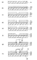
(LED照明シートの各部材)
次に、LED照明シート20を構成する各部材について説明する。図6に示すように、LED照明シート20は、フレキシブル配線基板30と、フレキシブル配線基板30上に配置された複数のLEDチップ21とを備えている。このうちフレキシブル配線基板30は、可撓性を有する基板フィルム31と、基板フィルム31の表面(発光面側の面)に形成された金属配線部32とを有している。金属配線部32は、接着剤層33を介して基板フィルム31に積層されている。
(Each member of LED lighting sheet)
Next, each member constituting the
各LEDチップ21は、金属配線部32に導通可能な態様で実装されている。このLED照明シート20においては、LEDチップ21がフレキシブル配線基板30に実装されていることにより、複数のLEDチップ21を、所望の高い密度で配置することが可能である。
Each
LED照明シート20のうち、LEDチップ21、レギュレータ45、およびコネクタ44A、44Bが設けられている領域及びその周辺領域を除く領域を覆って、光反射性絶縁保護膜34が形成されている。この光反射性絶縁保護膜34は、金属配線部32を覆うように配置されている。光反射性絶縁保護膜34は、LED照明シート20の耐マイグレーション特性の向上に寄与する絶縁機能と、LED照明シート20により作られる光環境の向上に寄与する光反射機能とを兼ね備える層である。この層は、白色顔料を含む絶縁性の樹脂組成物により形成される。前述の金属配線部32と後述の透明保護膜35のみで、耐マイグレーション特性および光反射機能が得られる場合には、光反射性絶縁保護膜34がない構造も可能である。
The light-reflecting insulating
また、光反射性絶縁保護膜34及びLEDチップ21を覆うように、透明保護膜35が形成されている。透明保護膜35は、主としてLED照明シート20の防水性を確保するためにその最表面(最も発光面側に位置する面)に形成される樹脂性の膜である。
Further, a transparent
金属配線部32上には、ハンダ部36が設けられている。各LEDチップ21は、それぞれハンダ部36を介して、金属配線部32に電気的に接続されている。
A
(基板フィルム)
基板フィルム31は、可撓性を有する樹脂フィルムを用いることができる。なお、本明細書中、「可撓性を有する」とは、「曲率半径を少なくとも1m以下、好ましくは50cm、より好ましくは30cm、更に好ましくは10cm、特に好ましくは5cmに曲げることが可能であること」をいう。
(Substrate film)
As the
基板フィルム31の材料としては、耐熱性及び絶縁性が高い熱可塑性樹脂が用いられても良い。このような樹脂として、耐熱性と加熱時の寸法安定性、機械的強度、及び耐久性に優れるポリイミド樹脂(PI)や、ポリエチレンナフタレート(PEN)を用いることができる。中でも、アニール処理等の耐熱性向上処理を施すことによって耐熱性と寸法安定性を向上させたポリエチレンナフタレート(PEN)を好ましく用いることもできる。また、難燃性の無機フィラー等を添加することによって難燃性を向上させたポリエチレンテレフタレート(PET)を用いても良い。
As the material of the
基板フィルム31の厚さは、特に限定されないが、放熱経路としてボトルネックとはならないこと、耐熱性及び絶縁性を有するものであること、及び、製造コストのバランスとの観点から、概ね10μm以上500μm以下、好ましくは、50μm以上250μm以下であることが好ましい。また、ロール・トゥ・ロール方式による製造を行う場合の生産性を良好に維持する観点からも上記厚さ範囲内であることが好ましい。
The thickness of the
(接着剤層)
接着剤層33を形成する接着剤は、公知の樹脂系接着剤を適宜用いることができる。それらの樹脂接着剤のうち、ウレタン系、ポリカーボネート系、シリコーン系、エステル系またはエポキシ系の接着剤等を特に好ましく用いることができる。また、接着剤層33を形成する接着剤として、アクリル系粘着剤を用いても良い。
(Adhesive layer)
As the adhesive forming the
(金属配線部)
金属配線部32は、基板フィルム31の表面(発光面側の面)に金属箔等の導電性基材によって形成される配線パターンである。この金属配線部32は、基板フィルム31の表面へ接着剤層33を介してドライラミネート法によって形成されることが好ましい。金属配線部32は、上述した複数の金属配線部22を含む。複数の金属配線部22は、第1の金属配線部22Aと、第1の金属配線部22Aから離間して配置された第2の金属配線部22Bとを含む。第1の金属配線部22A及び第2の金属配線部22Bには、LEDチップ21が搭載され、LEDチップ21は、第1の金属配線部22A及び第2の金属配線部22Bに電気的に接続されている。第1の金属配線部22A及び第2の金属配線部22Bに供給される電力によりLEDチップ21が点灯するようになっている。
(Metal wiring part)
The
金属配線部32は、放熱性と電気伝導性を高い水準で両立させるものであることが好ましく、例えば銅箔を用いることができる。この場合、LEDチップ21からの放熱性が安定し、電気抵抗の増加を防げるので、LEDチップ21間の発光バラツキが小さくなって安定した発光が可能となる。また、LEDチップ21の寿命も延長される。更に、熱による基板フィルム31等の周辺部材の劣化も防止できるので、LED照明シート20の製品寿命も延長することができる。金属配線部32を形成する金属の例としては、上記の銅の他、アルミニウム、金、銀等の金属を挙げることができる。
The
金属配線部32の厚さは、フレキシブル配線基板30に要求される耐電流の大きさ等に応じて適宜設定すればよい。但し、リフロー方式等によるハンダ加工処理時の基板フィルム31の熱収縮による反りを抑制するためには、金属配線部32の厚さが10μm以上であることが好ましい。一方、金属配線部32の厚さは、50μm以下であることが好ましく、これにより、フレキシブル配線基板30の十分な可撓性を維持することができ、重量増大によるハンドリング性の低下等も抑止することができる。
The thickness of the
(ハンダ部)
ハンダ部36は、金属配線部32とLEDチップ21との接合を行うものである。このハンダによる接合は、リフロー方式、あるいは、レーザー方式の2方式のいずれかによることができる。
(Solder part)
The
(LEDチップ)
LEDチップ21は、P型半導体とN型半導体が接合されたPN接合部での発光を利用した発光素子である。LEDチップ21としては、P型電極及びN型電極をそれぞれ素子の上面及び下面に設けた構造であっても良く、素子の片面にP型電極及びN型電極の双方が設けられた構造であっても良い。
(LED chip)
The
本実施の形態において、各LEDチップ21としては、光束量の大きいものを用いることが好ましい。具体的には、LEDチップ21として、30lm以上の光束量を有しているものを用いるが好ましく、35lm以上の光束量を有しているものを用いることが更に好ましい。また、LEDチップ21としては、発光効率が高いものを選択することが好ましい。具体的には、LEDチップ21として、150lm/W以上の発光効率を有しているものを用いることが好ましく、180lm/W以上の発光効率を有しているものを用いることが更に好ましい。LEDチップ21の発光効率を150lm/W以上に高めることにより、LEDチップ21の実装数(密度)を下げ、LEDチップ21からのジュール熱による発熱を少なくすることができ、LEDチップ21からの熱による植物の育成のばらつきが発生しにくくなって収量の低下を抑制することができる。
In the present embodiment, it is preferable to use each
LED照明シート20は、上述の通り、高い放熱性を発揮することができる金属配線部32に、LEDチップ21を直接実装するものである。これにより、LEDチップ21を高密度で配置した場合においても、LEDチップ21の点灯時に発生する過剰な熱を金属配線部32を通して速やかに拡散し、基板フィルム31を介してLED照明シート20の外部へ十分放熱することができ、LEDチップ21からの熱による植物の育成のばらつきが発生しにくくなって収量の低下を抑制することができる。
As described above, the
(光反射性絶縁保護膜)
光反射性絶縁保護膜34は、LEDチップ21が設けられている領域及びその周辺領域を除く領域に形成される層である。この光反射性絶縁保護膜34は、十分な絶縁性を有することにより、フレキシブル配線基板30の耐マイグレーション特性を向上させる所謂レジスト層であり、かつLED照明シート20により作られる光環境の向上に寄与する光反射性を備えた光反射層である。
(Light reflective insulating protective film)
The light-reflecting insulating
光反射性絶縁保護膜34は、ウレタン系樹脂等をベース樹脂とし、酸化チタン等の無機フィラーからなる白色顔料を更に含有する各種の樹脂組成物により形成することができる。光反射性絶縁保護膜34を形成するために用いる樹脂組成物のベース樹脂としては、ウレタン系樹脂の他、アクリルウレタン系樹脂、ポリエステル系樹脂、フェノール系樹脂等を適宜用いることができる。光反射性絶縁保護膜34を形成する樹脂組成物のベース樹脂としては、透明保護膜35を形成する樹脂組成物と同一または同系の樹脂をベース樹脂とすることがより好ましい。透明保護膜35については、後述するように、アクリルウレタン系樹脂を主たる材料樹脂として用いることが好ましい。これより、透明保護膜35を形成する樹脂組成物のベース樹脂がアクリルウレタン系樹脂である場合には、光反射性絶縁保護膜34を形成するための樹脂組成物のベース樹脂はウレタン系樹脂またはアクリルウレタン系樹脂とすることがより好ましい。
The light-reflecting insulating
光反射性絶縁保護膜34を形成する樹脂組成物に白色顔料として含有させる無機フィラーとしては、酸化チタンの他、アルミナ、硫酸バリウム、マグネシア、チッ化アルミニウム、チッ化ホウ素、チタン酸バリウム、カオリン、タルク、炭酸カルシウム、酸化亜鉛、シリカ、マイカ粉、粉末ガラス、粉末ニッケル及び粉末アルミニウムから選ばれる少なくとも1種を用いることができる。
Examples of the inorganic filler contained as a white pigment in the resin composition forming the light-reflecting insulating
光反射性絶縁保護膜34の厚さは、5μm以上50μm以下であって、より好ましくは、7μm以上20μm以下である。光反射性絶縁保護膜34の厚さが、5μm未満であると、特に金属配線部32のエッジ部分において、光反射性絶縁保護膜が薄くなり、この金属配線を被覆できずに露出する場合は絶縁性が維持できなくなるリスクが大きくなる。一方、取扱い及び搬送等の際の基板湾曲から光反射性絶縁保護膜34を保持する観点から、光反射性絶縁保護膜34の厚さは、50μm以下であることが好ましい。
The thickness of the light-reflecting insulating
また、光反射性絶縁保護膜34は、波長400nm以上780nm以下における光線平均反射率が、いずれも65%以上であることが好ましく、70%以上であることがより好ましく、80%以上であることが更に好ましい。LED照明シート20は、例えば、酸化チタンを、ウレタン系またはアクリルウレタン系のベース樹脂100質量部に対して20質量部以上含有させることで、光反射性絶縁保護膜34の厚さを8μmとする場合における同層の上記光線反射率を75%以上とすることが可能である。
Further, the light-reflecting insulating
(透明保護膜)
透明保護膜35は、LEDチップ21を覆うように、LED照明シート20の最表面に形成されている。透明保護膜35は、防水性と透明性とを有する。透明保護膜35の防水性により、LED照明シート20を植物育成用光源として使用する場合の装置内部への水の侵入を防ぐことができる。全光束量が3000lm以上の光を照射するLED照明シート20では、LEDチップ21の性能を向上させる必要があり、特定のLEDチップ21が破損した場合の影響が大きくなる。そのためLEDチップ21が可能な限り破損しにくいようにすることは、リスク管理の観点で重要である。
(Transparent protective film)
The transparent
透明保護膜35は、アクリルウレタン系樹脂等をベース樹脂とする各種の樹脂組成物により形成することができる。透明保護膜35を形成するために用いる樹脂組成物のベース樹脂としては、アクリルウレタン系樹脂の他、ウレタン系樹脂、ポリエステル系樹脂、フェノール系樹等を適宜用いることができる。透明保護膜35を形成する樹脂組成物のベース樹脂としては、光反射性絶縁保護膜34を形成する樹脂組成物と同一または同系の樹脂をベース樹脂とすることがより好ましい。好ましい具体的な組合せとして、光反射性絶縁保護膜34を形成する樹脂組成物のベース樹脂をウレタン系樹脂とし、透明保護膜35を形成する同樹脂をアクリルウレタン系樹脂とする組合せを挙げることができる。
The transparent
透明保護膜35の厚さは、10μm以上40μm以下であり、好ましくは15μm以上30μm以下であり、より好ましくは20μm以上25μm以下である。透明保護膜35の厚さを上記範囲とすることにより、LED照明シート20の良好な可撓性や薄さ、軽量性、及び植物育成用途において求められる良好な光学特性を維持することができる。また、LED照明シート20に対して植物育成用途に求められる十分な防水性をもたらすことができる。
The thickness of the transparent
透明保護膜35によるLED照明シート20の耐水性としては、LED照明シート20に対して植物育成用の水を散布した際に、LEDチップ21の劣化を抑制することが可能となる程度であれば特に限定されない。このような耐水性としては、IEC(国際電気標準会議)によって定められている防水・防塵の保護規格でIPX4以上を示すことが好ましい。IPX4以上の防水性は、あらゆる方向からの水の飛沫によってLEDチップ21に対して有害な影響が及ぼされない程度である。具体的には、LED照明シート20の法線方向に対して±180°の全範囲に5分間、10L/分の水量で散水ノズルから散水した際、LEDチップ21に対して有害な影響が及ぼされない程度とされる。
The water resistance of the
(LED照明シートの製造方法)
次に、本実施の形態によるLED照明シート20の製造方法について、図7(a)−(h)を参照して説明する。
(Manufacturing method of LED lighting sheet)
Next, a method of manufacturing the
まず、基板フィルム31を準備する(図7(a))。次に、基板フィルム31の表面に、金属配線部32の材料となる銅箔等の金属箔32Aを積層する(図7(b)(b))。金属箔32Aは、金属箔32Aを例えばウレタン系接着剤等の接着剤層33によって、基板フィルム31の表面に接着される。あるいは、金属箔32Aは、基板フィルム31の表面に電解メッキ方法や気相製膜法(スパッタリング、イオンプレーティング、電子ビーム蒸着、真空蒸着、化学蒸着等)により、直接形成しても良い。もしくは、金属箔32Aに基板フィルム31を直接溶着して形成しても良い。
First, the
次に、金属箔32Aの表面に、金属配線部32に要求される形状にパターニングされたエッチングマスク37を形成する(図7(c))。このエッチングマスク37は、金属配線部32となる金属箔32Aの配線パターンに対応する部分がエッチング液によって腐食しないように設けられる。エッチングマスク37を形成する方法は特に限定されず、例えば、フォトレジストまたはドライフィルムを、フォトマスクを通して感光させた後に現像することによって形成しても良く、インクジェットプリンター等の印刷技術により金属箔32Aの表面にエッチングマスクを形成してもよい。
Next, an etching mask 37 patterned in a shape required for the
次に、エッチングマスク37に覆われていない箇所に位置する金属箔32Aを浸漬液により除去する(図7(d))。これにより、金属箔32Aのうち、金属配線部32となる箇所以外の部分が除去される。
Next, the
その後、アルカリ性の剥離液を使用して、エッチングマスク37を除去する。これにより、エッチングマスク37が金属配線部32の表面から除去される(図7(e))。 The etching mask 37 is then removed using an alkaline stripper. As a result, the etching mask 37 is removed from the surface of the metal wiring portion 32 (FIG. 7 (e)).
続いて、金属配線部32上に光反射性絶縁保護膜34を積層形成する(図7(f))。光反射性絶縁保護膜34の形成は、光反射性絶縁保護膜34を構成する材料樹脂組成物を均一に塗工できる塗工手段であれば特に限定されず、例えば、スクリーン印刷、オフセット印刷、ディップコータ、刷毛塗り等の方法を使用することができる。または、光感光性を有する絶縁保護膜材料を全面に塗工し、必要な箇所のみフォトマスクを通して感光させた後に現像することによって光反射性絶縁保護膜34を形成しても良い。
Subsequently, the light-reflecting insulating
次に、金属配線部32上にLEDチップ21、レギュレータ45及びコネクタ44A、44Bを実装する(図7(g))。この場合、LEDチップ21は、金属配線部32にハンダ部36を介するハンダ加工によって接合される。このハンダ加工による接合は、リフロー方式、あるいは、レーザー方式によることができ、または導電性樹脂による接合でも良い。
Next, the
次いで、光反射性絶縁保護膜34、LEDチップ21、レギュレータ45及びコネクタ44A、44Bを覆うように透明保護膜35を形成する(図7(h))。この透明保護膜35は、透明樹脂組成物をスプレー処理により吹付けて形成する方法(以下、「スプレーコート法」という)、またはカーテンコート法により形成する方法により行うことが好ましい。スプレーコート法による透明保護膜35の形成は、例えば、アクリル系ポリウレタン樹脂を含むスプレーコート処理用の塗工液を、スプレー塗装機によってフレキシブル配線基板30上の所望の領域に噴霧して塗工膜を形成することにより行うことができる。カーテンコート法による透明保護膜35の形成は、例えば、アクリル系ポリウレタン樹脂を含むカーテンコート処理用の塗工液を、カーテン塗装機によってフレキシブル配線基板30上の所望の領域に滴下して塗工膜を形成することにより行うことができる。
Next, a transparent
なお、本実施の形態によるLED照明シート20は、上述した方法に限らず、従来公知のLEDチップ用のフレキシブル配線基板や、これにLEDチップを実装してなる各種のLEDモジュールを製造する公知の方法により製造することもできる。
The
(植物育成工場及び植物の育成棚)
図8は、本実施の形態によるLED照明シート20を用いた植物育成工場90の構成を模式的に示す図である。植物育成工場90は、建物91と、建物91の内部に配置された複数の植物の育成棚80を備えている。
(Plant growing factory and plant growing shelf)
FIG. 8 is a diagram schematically showing the configuration of a
図9に示すように、植物の育成棚80は、複数(4本)の支柱82と、支柱82に沿ってそれぞれ上下方向に間隔を空けて配置された複数の基板81とを有している。最上段の基板81を除く各基板81の上面には、植物PLを栽培するための培地領域が設けられている。最下段の基板81を除く各基板81の下面は、当該基板81の下方に位置する基板81に対して天井面を構成しており、LED照明シート20が並列に配置されている。この場合、制御部40はLED照明シート20から十分に離れた場所に配置される。このため、制御部40に近い位置にある植物PLと遠い位置にある植物PLとで、制御部40からの熱によって生育にばらつきが生じるおそれが少ない。また、基板81と、基板81の下面側に取り付けられたLED照明シート20とにより、植物の育成棚用の棚板83が構成される。あるいは、基板81と、基板81の下面側に取り付けられたLED照明モジュール10とにより、植物の育成棚用の棚板83が構成される。本実施の形態において、このような植物の育成棚用の棚板83(図9)、植物の育成棚80(図9)、及び植物の育成棚80を備えた植物育成工場90(図8)も提供する。
As shown in FIG. 9, the
本実施の形態によるLED照明シート20が可撓性と軽量性を有することにより、各基板81の下面へのLED照明シート20の取付けは、従来の直管型の照明装置等による取付けよりも容易に行うことができる。さらに、LED照明シート20が可撓性を有することにより、LED照明シート20を、様々なサイズや形状からなる天井面へ取り付けることができる。この結果、本実施の形態によるLED照明シート20は、様々な植物の育成棚80や植物育成工場90へ適用することができる。
Since the
また、LED照明シート20は、従来の直管型の照明装置と比較して薄型化されている。これにより、上下方向の基板81の間隔を狭めることができ、各植物の育成棚80に含まれる基板81の数を増やすことができる。この結果、単位面積あたりの植物PLの収穫量を増加することができる。
Further, the
なお、図10(a)(b)に示すように、LED照明シート20は、基板81の下面だけでなく、基板81の側面側にも配置しても良い。この側面側のLED照明シート20は、上方に位置する基板81から、当該基板81の下方に位置する基板81に向けて垂下されている。この場合、図10(a)に示すように、LED照明シート20は、下方に位置する基板81まで達していても良い。あるいは、図10(b)に示すように、LED照明シート20は、下方に位置する基板81まで達することなく、上下の基板81間に位置する空間の上部側のみを覆うようにしても良い。このように、LED照明シート20を、基板81の側面側にもさらに配置することにより、照度が弱くなりやすい基板81の周縁における光量を補い、LED照明シート20の輝度を面内で均一にすることができる。この結果、植物の成長を面内で均一にすることができ、育成する植物の収量の向上を図ることができる。
As shown in FIGS. 10A and 10B, the
また、図11に示すように、光反射シート84を棚板83の側面側にも配置しても良い。光反射シート84は、少なくとも内側(植物に面する側)にアルミニウムシート等の光反射性の材料を含んでいる。この光反射シート84は、上方に位置する棚板83から、当該棚板83の下方に位置する棚板83に向けて垂下されている。このように、光反射シート84を、棚板83の側面側に配置することにより、照度が弱くなりやすい棚板83の周縁における光量を補い、LED照明シート20の輝度を面内でより均一にすることができ、育成する植物の収量の向上を図ることができる。
Further, as shown in FIG. 11, the
(本実施の形態の作用)
次に、このような構成からなる本実施の形態の作用について述べる。
(Action of the present embodiment)
Next, the operation of the present embodiment having such a configuration will be described.
まず、LED照明モジュール10の電力入力部41(図2参照)を電源に接続し、電力入力部41に、例えば100V乃至240Vの任意の電圧をもつ交流の電流を供給する。次に、電力入力部41に入力された電流は、AC/DCコンバーター42によって定圧(例えば44V)の直流電圧に変換される。続いて、AC/DCコンバーター42からの直流電圧は、PWM制御部43において定電圧波形のパルス幅を調整され、LEDチップ21が所定の光束量となるように制御される。その後、PWM制御部43からの定電圧は、LED照明シート20に供給され、LEDチップ21が点灯する。
First, the power input unit 41 (see FIG. 2) of the
LED照明シート20のLEDチップ21からの光は、棚板83上に配置された植物に到達し、植物の成長を促進する。本実施の形態において、LED照明シート20の下方領域のうちLEDチップ21から50mm離れた任意の位置において、光合成光量子束密度(PPFD)を投入電力換算し、下方領域の平均値で規格化した値が0.2以上となっている。このように、LEDチップ21から50mm離れた任意の位置におけるPPFDが高められていることにより、LED照明シート20の輝度を高め、棚板83上に配置された植物の成長を促進することができる。
The light from the
一方、本願発明者らは、単にLED照明シートの輝度を高めただけでは、とりわけ植物の育成後期の段階で育成のスピードがばらついてしまい、かえって生育不良が増加することを見出した。具体的には、植物の育成後期の段階で、一部の植物が十分に育成されなかったり、一部の植物にチップバーンとよばれる育成障害が発生したりする場合がある。これは、植物の育成後期の段階では、植物の葉が上方のLED照明シートに接近するので、LEDチップに近い植物には光が多量に供給される一方、LEDチップから遠い植物には光が十分に供給されず、これらの植物の間で育成スピードに差が生じてしまうためであると考えられる。 On the other hand, the inventors of the present application have found that simply increasing the brightness of the LED lighting sheet causes variations in the growth speed, especially in the late stage of plant growth, and rather increases poor growth. Specifically, in the late stage of plant growth, some plants may not be sufficiently grown, or some plants may have a growth disorder called chip burn. This is because in the late stage of plant growth, the leaves of the plant approach the LED lighting sheet above, so that a large amount of light is supplied to the plant near the LED chip, while light is supplied to the plant far from the LED chip. This is thought to be because the plants are not sufficiently supplied and there is a difference in growth speed among these plants.
これに対して本実施の形態においては、LED照明シート20の下方領域のうちLEDチップ21から50mm離れた複数の位置において測定されたPPFDのばらつきを、平均値で規格化した際の標準偏差で0.5以下としている。このように、LEDチップ21から近い位置(すなわちLEDチップ21から50mm離れた位置)におけるPPFDのばらつきを低減することにより、LED照明シート20の下方におけるLEDチップ21からの光量を均一にしている。
On the other hand, in the present embodiment, the variation of PPFD measured at a plurality of positions 50 mm away from the
このように、LEDチップ21から50mm離れた位置でのPPFDのばらつきを低減することにより、LEDチップ21からの光の照射量が面内で均等となり、LED照明シート20の下方領域で光の照射量が不足する場所をなくすことができる(図12(a)参照)。すなわち本実施の形態においては、LED照明シート20のLEDチップ21同士の配置が面内で略均一となっているので、とりわけ植物の育成後期における植物の育成スピードを面内で均一にすることができる。また、LEDチップ21からの光の照射量が過剰になる場所もなくなるので、植物にチップバーンとよばれる成長障害が発生することも抑制することができる。
By reducing the variation in PPFD at a position 50 mm away from the
他方、比較例として、直管型LEDが配列されたLEDバーライト120を用いた場合(図12(b)参照)、LEDバーライト120の下方において輝度が面内でばらつくため、植物の育成スピードも面内でバラつくおそれがある。すなわち直管型LEDが配列されたLEDバーライト120は、LEDバーライト120同士の間が離れているため、光源から植物までの距離が近づくほど、PPFDのばらつきが大きくなる傾向がある。例えば、LEDバーライト120同士の間かつLEDバーライト120に近い領域には、輝度が不十分な領域Dが存在する。この場合、植物の育成後期において、一部の植物は輝度が不十分な領域Dに存在する。逆にLEDバーライト120に近すぎる植物には、過剰に光が照射されるおそれもある。このような問題に対処するため、LEDバーライト120においては、植物と照明との間の距離を大きく保つ必要があり、この結果上下の棚間距離を広く確保する必要が生じる。
On the other hand, as a comparative example, when the
これに対して本実施の形態によれば、LEDチップ21から50mm離れた位置でのPPFDのばらつきを低減することにより、光の輝度不足で育成が遅れる植物が発生したり、光の輝度が過剰になることによりチップバーンとなる植物が発生したりすることを抑えることができる。また本実施の形態によれば、植物とLEDチップ21との間の距離を大きく確保する必要がないため、上下の棚板83間の距離を近づけることができ、省スペース化を実現することができる。
On the other hand, according to the present embodiment, by reducing the variation of PPFD at a position 50 mm away from the
また本実施の形態によれば、LEDチップ21は、10個以上直列に配置され、このLEDチップ21の列が4列以上並列に配置されている。これにより、LEDチップ21を面内で均一に配置するとともに、LEDチップ21の配列を並列化し、LEDチップ21が破損した際のリスクを分散することができる。
Further, according to the present embodiment, 10 or
また本実施の形態によれば、LEDチップ21は、透明保護膜35によって覆われているので、植物の育成時に飛散する水分からLEDチップ21を保護することができる。
Further, according to the present embodiment, since the
また本実施の形態によれば、LED照明シート20の最も厚い部分における厚みが5mm以下であるので、植物の育成棚80の上下の基板81間の距離を減らし、基板81の数を増やすことにより、単位面積あたりの植物の収量を増加することができる。
Further, according to the present embodiment, since the thickness of the thickest portion of the
[実施例]
次に、本実施の形態における具体的実施例について説明する。
[Example]
Next, a specific example in the present embodiment will be described.
(LED照明シートの作成)
実施例1、2の育成棚及び比較例1、2の育成棚をそれぞれ以下の通り準備した。
(Creation of LED lighting sheet)
The growing shelves of Examples 1 and 2 and the growing shelves of Comparative Examples 1 and 2 were prepared as follows.
(実施例1)
560mm×390mmサイズのフィルム基板(ポリエチレンナフタレート、厚さ50μm)の一方の表面に、金属配線部を形成するための銅箔(厚さ35μm)を積層し、その後、金属配線用の銅箔についてエッチング処理をして、全ての実施例及び比較例において同一パターンの金属配線部を構成した。そして、基板フィルム及び金属配線部上に、ウレタン系樹脂をベース樹脂とし、このベース樹脂に対して20質量%の割合で酸化チタンを添加してなる絶縁性インキを用いてスクリーン印刷により厚さ10μmの光反射性絶縁保護膜を形成した。次に、金属配線部に、複数のLEDチップ(「NFSW757G−V2」(日亜化学工業社製))を、X方向に40mmピッチ、Y方向に35mmピッチで、14個の列を10列、ハンダ加工により実装した。更に、上記の絶縁性保護膜及びLEDチップを被覆する透明保護膜を、スプレーコート法により形成した。以上の通り作製したLED照明シートは、全光束量が3950lmであり、総投入電力が72Wであり、LEDチップから照射される光の色温度は5000Kであった。このLED照明シートを育成棚の基板の下面に2枚配置し、実施例1の育成棚とした。
(Example 1)
A copper foil (
(実施例2)
光反射シート(図11参照)を棚板の側面側に設けたこと、以外は、実施例1と同様に作製した育成棚を、実施例2の育成棚とした。
(Example 2)
The growing shelf produced in the same manner as in Example 1 was used as the growing shelf of Example 2, except that the light reflecting sheet (see FIG. 11) was provided on the side surface side of the shelf board.
(比較例1)
市販の直管型LEDが配列されたLEDバーライト(「TECO−L40N1−50NH−T8」(東神電気株式会社製))を育成棚の基板の下面に2本配置し、比較例1の育成棚とした。この場合、LEDバーライトは、全光束量が2300lmであり、投入電力が46Wであり、照射される光の色温度は5000Kであった。
(Comparative Example 1)
Two LED bar lights (“TECO-L40N1-50NH-T8” (manufactured by Toshin Electric Co., Ltd.)) in which commercially available straight tube type LEDs are arranged are arranged on the lower surface of the substrate of the growing shelf, and the growing of Comparative Example 1 is performed. It was a shelf. In this case, the LED bar light had a total luminous flux of 2300 lm, an input power of 46 W, and a color temperature of the emitted light of 5000 K.
(比較例2)
光反射シート(図11参照)を棚板の側面側に設けたこと、以外は、比較例1と同様に作製した育成棚を、比較例2の育成棚とした。
(Comparative Example 2)
The growing shelf produced in the same manner as in Comparative Example 1 was used as the growing shelf of Comparative Example 2, except that the light reflecting sheet (see FIG. 11) was provided on the side surface side of the shelf board.
実施例1、2及び比較例1、2の育成棚について、光合成光量子束密度(PPFD)をそれぞれ測定した。この場合、実施例1、2について、総投入電力を比較例1、2と同等になるよう調光装置にて調整し、それぞれLED照明シートの下方領域に含まれる複数の箇所(合計24箇所)でPPFDを測定した。また、比較例1、2の育成棚についても、実施例1、2の場合と同様の領域に含まれる複数の箇所(合計24箇所)でPPFDを測定した。なお、光合成光量子束密度(PPFD)は、光量子計(米国LI−COR社製、光量子センサーLI−190RおよびライトメーターLI−250A)により測定した。この場合、実施例1、2及び比較例1、2の育成棚について、それぞれLEDチップから50mm離れた箇所と200mm離れた箇所とについてPPFDを測定し、投入電力換算した後に下方領域の平均値で規格化した値をそれぞれ算出した。また、LEDチップから50mm離れた箇所と200mm離れた箇所とのそれぞれについて、PPFDを測定した値を平均値で規格化し、標準偏差を算出し、PPFDのばらつきとした。
The photosynthetic photon flux density (PPFD) was measured for the growing shelves of Examples 1 and 2 and Comparative Examples 1 and 2, respectively. In this case, for Examples 1 and 2, the total input power is adjusted by the dimming device so as to be equivalent to that of Comparative Examples 1 and 2, and a plurality of locations (24 locations in total) included in the lower region of the LED lighting sheet, respectively. The PPFD was measured with. Further, with respect to the growing shelves of Comparative Examples 1 and 2, PPFD was measured at a plurality of places (24 places in total) included in the same area as in the cases of Examples 1 and 2. The photosynthetic photon flux density (PPFD) was measured with a photon meter (photon sensor LI-190R and light meter LI-250A manufactured by LI-COR, USA). In this case, for the growing shelves of Examples 1 and 2 and Comparative Examples 1 and 2, the PPFD was measured at a location 50 mm away from the LED chip and at a
続いて、実施例1、2及び比較例1、2の育成棚を用いて、植物(極早生シスコ)を実際に栽培した。その後、生育した植物の育成量として生体重(g/m2)を測定し、これを投入電力で除することにより、投入電力あたりの生体重(g/m2/W)を算出した。この生体重の測定は、栽培終了後のレタスの外観評価からチップバーン(葉先枯れ)部を除去した形で、地上部生体重を栽培パネル毎に計測し平米あたりの重量に計算することで算出した。以上の評価結果を表1に示す。 Subsequently, the plants (very early Cisco) were actually cultivated using the growing shelves of Examples 1 and 2 and Comparative Examples 1 and 2. Then, the living body weight (g / m 2 ) was measured as the amount of growth of the grown plant, and the living body weight (g / m 2 / W) per input power was calculated by dividing this by the input power. This bioweight is measured by measuring the above-ground bioweight for each cultivation panel and calculating the weight per square meter in the form of removing the chip burn (withered leaf tips) from the appearance evaluation of lettuce after cultivation. Calculated. The above evaluation results are shown in Table 1.

上記表1に示すように、実施例1、2の育成棚と比較例1、2の育成棚とを比較した場合、LEDチップから200mm離れた箇所におけるPPFDのばらつきに大きな差は見られなかったが、LEDチップから50mm離れた箇所ではPPFDのばらつきが大きくなった。このように、LED照明シート(実施例1、2)を用いた場合、直管型LEDが配列されたLEDバーライト(比較例1、2)を用いた場合と比較して、光源に近い位置でのPPFDのばらつきを低減することができた。
As shown in Table 1 above, when the growing shelves of Examples 1 and 2 and the growing shelves of Comparative Examples 1 and 2 were compared, there was no significant difference in the variation of PPFD at a
また、実施例1、2の育成棚を用いた場合、比較例1、2の育成棚を用いた場合よりも、投入電力あたりの植物の生体重を増加させることができた。さらに、実施例1、2の育成棚を用いた場合、比較例1、2の育成棚を用いた場合と異なり、チップバーン発生に差が見られた。このように、実施例1、2の育成棚を用いた場合、比較例1、2の育成棚を用いた場合と比較して、LEDチップから50mm離れた箇所でのPPFDのばらつきが低減されているので、光源直下の光強度ムラが少なく、光強度と正の相関で増えるチップバーンの発生が抑えられ、除去されるはずの不良部が少なくなったため、高い生産性につながったと考えられる。 In addition, when the growing shelves of Examples 1 and 2 were used, the living weight of the plant per input power could be increased as compared with the case of using the growing shelves of Comparative Examples 1 and 2. Further, when the growing shelves of Examples 1 and 2 were used, a difference was observed in the occurrence of chip burn, unlike the case of using the growing shelves of Comparative Examples 1 and 2. As described above, when the growing shelves of Examples 1 and 2 are used, the variation of PPFD at a position 50 mm away from the LED chip is reduced as compared with the case of using the growing shelves of Comparative Examples 1 and 2. Therefore, it is considered that the unevenness of the light intensity directly under the light source is small, the occurrence of chip burn that increases in a positive correlation with the light intensity is suppressed, and the number of defective parts that should be removed is reduced, which leads to high productivity.
上記実施の形態および変形例に開示されている複数の構成要素を必要に応じて適宜組合せることも可能である。あるいは、上記実施の形態および変形例に示される全構成要素から幾つかの構成要素を削除してもよい。 It is also possible to appropriately combine a plurality of components disclosed in the above-described embodiments and modifications as necessary. Alternatively, some components may be removed from all the components shown in the above embodiments and modifications.
10 LED照明モジュール
20 LED照明シート
21 LEDチップ
22 金属配線部
30 フレキシブル配線基板
31 基板フィルム
32 金属配線部
33 接着剤層
34 光反射性絶縁保護膜
35 透明保護膜
36 ハンダ部
40 制御部
41 電力入力部
42 AC/DCコンバーター
43 PWM制御部
44A 第1コネクタ
44B 第2コネクタ
45 レギュレータ
46 電力供給ライン
80 植物の育成棚
81 基板
82 支柱
83 植物の育成棚用の棚板
84 光反射シート
90 植物育成工場
91 建物
10
Claims (7)
基板フィルムと、
前記基板フィルムの表面に形成された金属配線部と、
前記金属配線部上に形成された光反射性絶縁保護膜と、
前記光反射性絶縁保護膜及び前記複数のLEDチップを覆うように形成された透明保護膜と、を備え、
前記複数のLEDチップは、前記金属配線部に実装され、
前記動植物育成用のLED照明シートの下方領域のうち前記LEDチップから50mm離れた任意の位置において、光合成光量子束密度を投入電力換算し、下方領域の平均値で規格化した値が0.2以上であり、
前記動植物育成用のLED照明シートの下方領域のうち前記LEDチップから50mm離れた位置において測定された光合成光量子束密度のばらつきが、平均値で規格化した際の標準偏差で0.5以下であり、
前記LEDチップは、37mm以上50mm以下の間隔で10個以上直列に配置され、このLEDチップの列が37mm以上100mm以下の間隔で4列以上並列に配置されており、
前記光反射性絶縁保護膜は、白色顔料を含むとともに、波長400nm以上780nm以下における光線平均反射率が、いずれも65%以上であり、
前記金属配線部の厚さは、10μm以上50μm以下であり、
前記透明保護膜の厚さは、10μm以上40μm以下である、動植物育成用のLED照明シート。 An LED lighting sheet for growing animals and plants in which multiple LED chips are arranged.
Substrate film and
The metal wiring portion formed on the surface of the substrate film and
A light-reflecting insulating protective film formed on the metal wiring portion and
The light-reflecting insulating protective film and the transparent protective film formed so as to cover the plurality of LED chips are provided.
The plurality of LED chips are mounted on the metal wiring portion, and the plurality of LED chips are mounted on the metal wiring portion.
At an arbitrary position 50 mm away from the LED chip in the lower region of the LED lighting sheet for growing animals and plants, the photosynthetic photon flux density is converted into input power, and the value normalized by the average value of the lower region is 0.2 or more. And
The variation in the photosynthetic photon flux density measured at a position 50 mm away from the LED chip in the lower region of the LED lighting sheet for growing animals and plants is 0.5 or less as the standard deviation when standardized by the average value. ,
Ten or more LED chips are arranged in series at intervals of 37 mm or more and 50 mm or less, and four or more rows of LED chips are arranged in parallel at intervals of 37 mm or more and 100 mm or less .
The light-reflecting insulating protective film contains a white pigment and has a light average reflectance of 65% or more at a wavelength of 400 nm or more and 780 nm or less.
The thickness of the metal wiring portion is 10 μm or more and 50 μm or less.
An LED lighting sheet for growing animals and plants , wherein the thickness of the transparent protective film is 10 μm or more and 40 μm or less.
請求項1又は2記載の動植物育成用のLED照明シートと、
前記動植物育成用のLED照明シートに電気的に接続された制御部と、を備えた、動植物育成用のLED照明モジュール。 An LED lighting module for growing animals and plants
The LED lighting sheet for growing animals and plants according to claim 1 or 2,
An LED lighting module for growing animals and plants, comprising a control unit electrically connected to the LED lighting sheet for growing animals and plants.
基板と、
前記基板に取り付けられた、請求項1又は2記載の動植物育成用のLED照明シートまたは請求項3記載の動植物育成用のLED照明モジュールと、を備えた、動植物の育成棚用の棚板。 It is a shelf board for growing animals and plants,
With the board
A shelf board for growing animals and plants, comprising the LED lighting sheet for growing animals and plants according to claim 1 or 2 or the LED lighting module for growing animals and plants according to claim 3 , which is attached to the substrate.
棚板を備え、
前記棚板は、基板の下面側に取り付けられた、請求項1又は2記載の動植物育成用のLED照明シートまたは請求項3記載の動植物育成用のLED照明モジュールを備えた、動植物の育成棚。 It is a breeding shelf for animals and plants.
Equipped with shelves
The shelf board is an animal and plant growing shelf provided with the LED lighting sheet for growing animals and plants according to claim 1 or 2 or the LED lighting module for growing animals and plants according to claim 3 , which is attached to the lower surface side of the substrate.
前記建物の内部に配置された、請求項5又は6記載の動植物の育成棚と、を備えた、動植物育成工場。 Building and
An animal and plant growing factory provided with the animal and plant growing shelves according to claim 5 or 6 , which are arranged inside the building.
Priority Applications (7)
| Application Number | Priority Date | Filing Date | Title |
|---|---|---|---|
| JP2019017453A JP6953461B2 (en) | 2019-02-01 | 2019-02-01 | LED lighting sheet for growing animals and plants, LED lighting module for growing animals and plants, shelf board for growing shelves for animals and plants, growing shelves for animals and plants, and plant for growing animals and plants. |
| PCT/JP2020/002422 WO2020158584A1 (en) | 2019-02-01 | 2020-01-23 | Led illumination sheet for growth of animals and plants, led illumination module for growth of animals and plants, shelf board for shelf for growth of animals and plants, shelf for growth of animals and plants, and animal and plant growth factory |
| US17/427,758 US11892144B2 (en) | 2019-02-01 | 2020-01-23 | LED lighting sheet for animal/plant growth, LED lighting module for animal/plant growth, shelf for animal/plant growth rack, animal/plant growth rack, and animal/plant growth factory |
| EP20749373.5A EP3918907A4 (en) | 2019-02-01 | 2020-01-23 | Led illumination sheet for growth of animals and plants, led illumination module for growth of animals and plants, shelf board for shelf for growth of animals and plants, shelf for growth of animals and plants, and animal and plant growth factory |
| TW112115903A TW202332864A (en) | 2019-02-01 | 2020-01-30 | LED lighting sheet for animal/plant growth, LED lighting module for animal/plant growth, shelf for animal/plant growth rack, animal/plant growth rack, and animal/plant growth factory |
| TW109102919A TWI802782B (en) | 2019-02-01 | 2020-01-30 | LED lighting sheets for animal and plant breeding, LED lighting modules for animal and plant breeding, shed panels for animal and plant breeding sheds, animal and plant breeding sheds and animal and plant breeding factories |
| JP2020193702A JP6969657B2 (en) | 2019-02-01 | 2020-11-20 | LED lighting sheet for growing animals and plants, LED lighting module for growing animals and plants, shelf board for growing shelves for animals and plants, shelf for growing animals and plants, and plant for growing animals and plants. |
Applications Claiming Priority (1)
| Application Number | Priority Date | Filing Date | Title |
|---|---|---|---|
| JP2019017453A JP6953461B2 (en) | 2019-02-01 | 2019-02-01 | LED lighting sheet for growing animals and plants, LED lighting module for growing animals and plants, shelf board for growing shelves for animals and plants, growing shelves for animals and plants, and plant for growing animals and plants. |
Related Child Applications (1)
| Application Number | Title | Priority Date | Filing Date |
|---|---|---|---|
| JP2020193702A Division JP6969657B2 (en) | 2019-02-01 | 2020-11-20 | LED lighting sheet for growing animals and plants, LED lighting module for growing animals and plants, shelf board for growing shelves for animals and plants, shelf for growing animals and plants, and plant for growing animals and plants. |
Publications (3)
| Publication Number | Publication Date |
|---|---|
| JP2020124132A JP2020124132A (en) | 2020-08-20 |
| JP2020124132A5 JP2020124132A5 (en) | 2020-10-01 |
| JP6953461B2 true JP6953461B2 (en) | 2021-10-27 |
Family
ID=71842198
Family Applications (1)
| Application Number | Title | Priority Date | Filing Date |
|---|---|---|---|
| JP2019017453A Active JP6953461B2 (en) | 2019-02-01 | 2019-02-01 | LED lighting sheet for growing animals and plants, LED lighting module for growing animals and plants, shelf board for growing shelves for animals and plants, growing shelves for animals and plants, and plant for growing animals and plants. |
Country Status (5)
| Country | Link |
|---|---|
| US (1) | US11892144B2 (en) |
| EP (1) | EP3918907A4 (en) |
| JP (1) | JP6953461B2 (en) |
| TW (2) | TWI802782B (en) |
| WO (1) | WO2020158584A1 (en) |
Families Citing this family (2)
| Publication number | Priority date | Publication date | Assignee | Title |
|---|---|---|---|---|
| US20230003369A1 (en) * | 2020-02-18 | 2023-01-05 | DemeGrow, Inc | Contolled grow-light container systems |
| US20230292678A1 (en) * | 2022-03-18 | 2023-09-21 | Global Garden LLC | Uniformity of light dispersion |
Family Cites Families (16)
| Publication number | Priority date | Publication date | Assignee | Title |
|---|---|---|---|---|
| US5012609A (en) * | 1988-12-12 | 1991-05-07 | Automated Agriculture Associates, Inc. | Method and apparatus for irradiation of plants using optoelectronic devices |
| JP2008091459A (en) * | 2006-09-29 | 2008-04-17 | Rohm Co Ltd | Led illumination apparatus and manufacturing method thereof |
| JP2008118957A (en) | 2006-11-15 | 2008-05-29 | Shokubutsu Kojo Kaihatsu:Kk | Full controlling type organic cultivation type plant factory |
| US20120113650A1 (en) * | 2010-11-10 | 2012-05-10 | E.I. Du Pont De Nemours And Company | Insulating white glass paste for forming insulating reflective layer |
| JP6230777B2 (en) * | 2012-01-30 | 2017-11-15 | 新光電気工業株式会社 | WIRING BOARD, WIRING BOARD MANUFACTURING METHOD, AND LIGHT EMITTING DEVICE |
| JP2013251230A (en) | 2012-06-04 | 2013-12-12 | Yamato Kogyo Kk | Lighting device and lighting system |
| JP2014122296A (en) * | 2012-12-21 | 2014-07-03 | Konica Minolta Inc | Sealing material precursor solution for light-emitting device, sealing material for light-emitting device using the same, led device, and method for producing the led device |
| JP2015138902A (en) | 2014-01-23 | 2015-07-30 | シチズンホールディングス株式会社 | Light-emitting device |
| KR101502960B1 (en) * | 2014-10-29 | 2015-03-17 | 농업회사법인 주식회사 퓨쳐그린 | LED lighting module for optimizing inception growth efficiency of plant, LED lighting apparatus for plant-culture factory using the same |
| EP3875839A1 (en) * | 2015-09-29 | 2021-09-08 | Cabatech, LLC | Horticulture grow lights |
| WO2017065766A1 (en) * | 2015-10-14 | 2017-04-20 | Starlite Led Inc. | Led flip chip plant grow light |
| US10165735B1 (en) * | 2016-06-29 | 2019-01-01 | Full Spectrum Industries Corp. | Dynamic plant lighting systems and methods |
| JP6955918B2 (en) | 2017-07-03 | 2021-10-27 | 株式会社ディスコ | Substrate processing method |
| JP2019016631A (en) * | 2017-07-03 | 2019-01-31 | 大日本印刷株式会社 | Method of manufacturing led module |
| WO2020153448A1 (en) * | 2019-01-24 | 2020-07-30 | 大日本印刷株式会社 | Led illumination sheet for animal and plant cultivation, led illumination module for animal and plant cultivation, shelf plate for cultivation shelf for animals and plants, cultivation shelf for animals and plants, animal and plant cultivation factory, and led illumination device for animal and plant cultivation |
| US11477945B2 (en) * | 2019-03-13 | 2022-10-25 | Current Lighting Solutions, Llc | Horticulture lighting device |
-
2019
- 2019-02-01 JP JP2019017453A patent/JP6953461B2/en active Active
-
2020
- 2020-01-23 US US17/427,758 patent/US11892144B2/en active Active
- 2020-01-23 EP EP20749373.5A patent/EP3918907A4/en active Pending
- 2020-01-23 WO PCT/JP2020/002422 patent/WO2020158584A1/en unknown
- 2020-01-30 TW TW109102919A patent/TWI802782B/en active
- 2020-01-30 TW TW112115903A patent/TW202332864A/en unknown
Also Published As
| Publication number | Publication date |
|---|---|
| TWI802782B (en) | 2023-05-21 |
| US11892144B2 (en) | 2024-02-06 |
| EP3918907A1 (en) | 2021-12-08 |
| TW202038703A (en) | 2020-11-01 |
| US20220243901A1 (en) | 2022-08-04 |
| WO2020158584A1 (en) | 2020-08-06 |
| TW202332864A (en) | 2023-08-16 |
| EP3918907A4 (en) | 2022-10-19 |
| JP2020124132A (en) | 2020-08-20 |
Similar Documents
| Publication | Publication Date | Title |
|---|---|---|
| TWI837289B (en) | LED lighting sheets for animal and plant breeding, LED lighting modules for animal and plant breeding, shed boards for animal and plant breeding, animal and plant breeding sheds, animal and plant breeding factories, and LED lighting devices for animal and plant breeding | |
| JP7051725B2 (en) | LED lighting sheet for growing animals and plants, LED lighting module for growing animals and plants, shelf board for growing shelves for animals and plants, shelf for growing animals and plants, and plant for growing animals and plants. | |
| JP7528173B2 (en) | Plant cultivation facility and plant cultivation method | |
| JP6780715B2 (en) | LED lighting device for growing animals and plants, LED lighting module for growing animals and plants, shelf board for growing shelves for animals and plants, growing shelves for animals and plants, and plant for growing animals and plants. | |
| JP6969657B2 (en) | LED lighting sheet for growing animals and plants, LED lighting module for growing animals and plants, shelf board for growing shelves for animals and plants, shelf for growing animals and plants, and plant for growing animals and plants. | |
| JP6953461B2 (en) | LED lighting sheet for growing animals and plants, LED lighting module for growing animals and plants, shelf board for growing shelves for animals and plants, growing shelves for animals and plants, and plant for growing animals and plants. | |
| JP2021022572A (en) | Led lighting device for animal/plant growth, led lighting module for animal/plant growth, shelf board for animal/plant growth shelf, animal/plant growth shelf, and animal/plant growth factory | |
| JP7118904B2 (en) | Animal and plant growing LED lighting sheet, animal and plant growing LED lighting module, animal and plant growing shelf plate, animal and plant growing shelf, and animal and plant growing factory | |
| JP7385832B2 (en) | LED lighting sheets for growing animals and plants, LED lighting modules for growing animals and plants, shelves for growing shelves for animals and plants, shelves for growing animals and plants, and plants for growing animals and plants | |
| JP7051732B2 (en) | LED lighting modules for growing animals and plants, shelves for growing animals and plants, and plants and animals growing factories | |
| JP7535252B2 (en) | Plant and animal cultivation equipment | |
| JP7465459B2 (en) | LED lighting module for cultivating animals and plants, cultivating shelf for animals and plants, and cultivating factory for animals and plants | |
| JP7501197B2 (en) | LED lighting sheet for cultivating animals and plants, LED lighting module for cultivating animals and plants, shelf board for cultivating shelves for animals and plants, cultivating shelves for animals and plants, and plant and animal cultivating factory | |
| JP7404769B2 (en) | LED lighting sheet assembly for animal and plant growing shelves, animal and plant growing shelves, and animal and plant growing factories | |
| JP7340166B2 (en) | LED lighting sheets for growing animals and plants, LED lighting modules for growing animals and plants, shelves for growing shelves for animals and plants, shelves for growing animals and plants, and plants for growing animals and plants | |
| TW202426816A (en) | LED lighting sheets for animal and plant breeding, LED lighting modules for animal and plant breeding, shed boards for animal and plant breeding, animal and plant breeding sheds and animal and plant breeding factories | |
| JP2023034266A (en) | Led sheet, shelf board for shelf for raising animal and plant, shelf for raising animal and plant, and plant for raising animal and plant |
Legal Events
| Date | Code | Title | Description |
|---|---|---|---|
| A521 | Request for written amendment filed |
Free format text: JAPANESE INTERMEDIATE CODE: A523 Effective date: 20200702 |
|
| A621 | Written request for application examination |
Free format text: JAPANESE INTERMEDIATE CODE: A621 Effective date: 20200702 |
|
| A871 | Explanation of circumstances concerning accelerated examination |
Free format text: JAPANESE INTERMEDIATE CODE: A871 Effective date: 20200702 |
|
| A975 | Report on accelerated examination |
Free format text: JAPANESE INTERMEDIATE CODE: A971005 Effective date: 20200710 |
|
| A131 | Notification of reasons for refusal |
Free format text: JAPANESE INTERMEDIATE CODE: A131 Effective date: 20200717 |
|
| A521 | Request for written amendment filed |
Free format text: JAPANESE INTERMEDIATE CODE: A523 Effective date: 20200806 |
|
| A02 | Decision of refusal |
Free format text: JAPANESE INTERMEDIATE CODE: A02 Effective date: 20200821 |
|
| A521 | Request for written amendment filed |
Free format text: JAPANESE INTERMEDIATE CODE: A523 Effective date: 20201120 |
|
| C60 | Trial request (containing other claim documents, opposition documents) |
Free format text: JAPANESE INTERMEDIATE CODE: C60 Effective date: 20201120 |
|
| A911 | Transfer to examiner for re-examination before appeal (zenchi) |
Free format text: JAPANESE INTERMEDIATE CODE: A911 Effective date: 20201201 |
|
| C21 | Notice of transfer of a case for reconsideration by examiners before appeal proceedings |
Free format text: JAPANESE INTERMEDIATE CODE: C21 Effective date: 20201204 |
|
| A912 | Re-examination (zenchi) completed and case transferred to appeal board |
Free format text: JAPANESE INTERMEDIATE CODE: A912 Effective date: 20201225 |
|
| C211 | Notice of termination of reconsideration by examiners before appeal proceedings |
Free format text: JAPANESE INTERMEDIATE CODE: C211 Effective date: 20210105 |
|
| C22 | Notice of designation (change) of administrative judge |
Free format text: JAPANESE INTERMEDIATE CODE: C22 Effective date: 20210507 |
|
| C22 | Notice of designation (change) of administrative judge |
Free format text: JAPANESE INTERMEDIATE CODE: C22 Effective date: 20210713 |
|
| C23 | Notice of termination of proceedings |
Free format text: JAPANESE INTERMEDIATE CODE: C23 Effective date: 20210727 |
|
| C03 | Trial/appeal decision taken |
Free format text: JAPANESE INTERMEDIATE CODE: C03 Effective date: 20210831 |
|
| C30A | Notification sent |
Free format text: JAPANESE INTERMEDIATE CODE: C3012 Effective date: 20210831 |
|
| A61 | First payment of annual fees (during grant procedure) |
Free format text: JAPANESE INTERMEDIATE CODE: A61 Effective date: 20210929 |
|
| R150 | Certificate of patent or registration of utility model |
Ref document number: 6953461 Country of ref document: JP Free format text: JAPANESE INTERMEDIATE CODE: R150 |