JP2020184846A - Power supplying device - Google Patents
Power supplying device Download PDFInfo
- Publication number
- JP2020184846A JP2020184846A JP2019088745A JP2019088745A JP2020184846A JP 2020184846 A JP2020184846 A JP 2020184846A JP 2019088745 A JP2019088745 A JP 2019088745A JP 2019088745 A JP2019088745 A JP 2019088745A JP 2020184846 A JP2020184846 A JP 2020184846A
- Authority
- JP
- Japan
- Prior art keywords
- carrier wave
- smoothing capacitor
- inverter
- inverter device
- phase
- Prior art date
- Legal status (The legal status is an assumption and is not a legal conclusion. Google has not performed a legal analysis and makes no representation as to the accuracy of the status listed.)
- Pending
Links
Images


Landscapes
- Inverter Devices (AREA)
Abstract
【課題】複数のインバータ装置の駆動に用いられる搬送波の位相を適切に調整する。【解決手段】電力供給装置10は、直流電源200と、前記直流電源にそれぞれ平滑コンデンサを介して接続される2つのインバータ装置211、212と、前記平滑コンデンサの電流をそれぞれ取得する2つの電流センサ281、282と、を備え、前記2つのインバータ装置のうちの第1インバータ装置211は、第1平滑コンデンサC1に流れる第1平滑コンデンサ電流Ic1が判定値Ithを超えた場合に前記第1インバータ装置を駆動する第1搬送波cw1の位相を遅らせ、前記2つのインバータ装置のうちの前記第1インバータ装置と異なる第2インバータ装置211は、第2平滑コンデンサC2に流れる第2平滑コンデンサ電流Ic2が判定値Ithを超えた場合に前記第2インバータ装置を駆動する第2搬送波cw2の位相を進ませる。【選択図】図5APROBLEM TO BE SOLVED: To appropriately adjust the phase of a carrier wave used for driving a plurality of inverter devices. A power supply device 10 includes a DC power supply 200, two inverter devices 211 and 212 connected to the DC power supply via a smoothing capacitor, and two current sensors that acquire the current of the smoothing capacitor, respectively. The first inverter device 211 of the two inverter devices includes 281 and 282, and the first inverter device 211 is the first inverter device when the first smoothing capacitor current Ic1 flowing through the first smoothing capacitor C1 exceeds the determination value Is. In the second inverter device 211 of the two inverter devices, which delays the phase of the first carrier cw1 and is different from the first inverter device, the second smoothing capacitor current Ic2 flowing through the second smoothing capacitor C2 is a determination value. When It exceeds Is, the phase of the second carrier cw2 that drives the second inverter device is advanced. [Selection diagram] FIG. 5A
Description
本開示は、電力供給装置に関し、特に複数のインバータ装置を有する電力供給装置に関する。 The present disclosure relates to a power supply device, and more particularly to a power supply device having a plurality of inverter devices.
従来、負荷を駆動する複数のインバータ装置を備える装置において、2つのインバータ装置のスイッチングの位相をずらすことで、騒音や出力の乱れを改善させることが知られている(例えば特許文献1、特許文献2)。
Conventionally, in a device including a plurality of inverter devices for driving a load, it is known to improve noise and output disturbance by shifting the switching phases of the two inverter devices (for example,
しかし、こうした複数のインバータ装置を備える装置では、複数のインバータ装置に設けられている平滑コンデンサに流れる電流を適正に制御することは、考慮されていなかった。平滑コンデンサに流れる電流は、インバータ装置の配置により変化するため、一律の調整も困難であった。 However, in a device provided with such a plurality of inverter devices, proper control of the current flowing through the smoothing capacitors provided in the plurality of inverter devices has not been considered. Since the current flowing through the smoothing capacitor changes depending on the arrangement of the inverter device, it is difficult to make a uniform adjustment.
本開示の一形態によれば、電力供給装置(10)が提供される。この電力供給装置は、直流電源(200)と、前記直流電源にそれぞれ平滑コンデンサを介して接続される2つのインバータ装置(211、212)と、前記平滑コンデンサの電流をそれぞれ取得する2つの電流センサ(281、282)と、を備え、前記2つのインバータ装置のうちの第1インバータ装置(211)は、第1平滑コンデンサ(C1)に流れる第1平滑コンデンサ電流(Ic1)が判定値(Ith)を超えた場合に前記第1インバータ装置の駆動に用いられる第1搬送波(cw1)の位相を遅らせ、前記2つのインバータ装置のうちの前記第1インバータ装置と異なる第2インバータ装置(211)は、第2平滑コンデンサ(C2)に流れる第2平滑コンデンサ電流(Ic2)が判定値(Ith)を超えた場合に前記第2インバータ装置の駆動に用いられる第2搬送波(cw2)に位相を進ませる。この形態によれば、2つの搬送波の位相差を適切に調整し、平滑コンデンサ電流を低減できる。 According to one form of the present disclosure, a power supply device (10) is provided. This power supply device includes a DC power supply (200), two inverter devices (211 and 212) connected to the DC power supply via a smoothing capacitor, and two current sensors that acquire the current of the smoothing capacitor, respectively. (281, 282), and the first inverter device (211) of the two inverter devices has a determination value (Ith) of the first smoothing capacitor current (Ic1) flowing through the first smoothing capacitor (C1). The second inverter device (211), which is different from the first inverter device among the two inverter devices, delays the phase of the first carrier (cw1) used for driving the first inverter device when the above value is exceeded. When the second smoothing capacitor current (Ic2) flowing through the second smoothing capacitor (C2) exceeds the determination value (Ith), the phase is advanced to the second carrier (cw2) used for driving the second inverter device. According to this form, the phase difference between the two carrier waves can be appropriately adjusted to reduce the smoothing capacitor current.
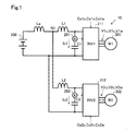
・第1実施形態:
図1に示す電力供給装置は、システム10は、直流電源200と、2つのインバータ装置211、212と、2個の平滑コンデンサC1、C2と、電流センサ281、282と、を備える。2つのインバータ装置211、212は、いずれも三相変調インバータ装置である。また、2つの電動モータ301、302は、いずれも三相モータである。
-First embodiment:
In the power supply device shown in FIG. 1, the
第1インバータ装置211は、第1平滑コンデンサC1を介して直流電源200に接続され、第2インバータ装置212は、第2平滑コンデンサC2を介して直流電源200に接続されている。図1のLaは、直流電源200から2つのインバータ装置211、212の分岐点N1までの配線インダクタであり、L1は、分岐点N1から第1平滑コンデンサC1までの配線インダクタであり、L2は、分岐点N1から第2平滑コンデンサC2までの配線インダクタである。配線インダクタLa、L1、L2の大きさは、主に各配線の長さに依存する。
The
図示しない制御部は、第1電動モータ301に要求される駆動力に応じて、第1インバータ装置211を駆動するための指令信号Cs1u、Cs1v、Cs1wを生成し、第2電動モータ302に要求される駆動力に応じて、第2インバータ装置212を駆動するための指令信号Cs2u、Cs2v、Cs2wを生成する。第1インバータ装置211は、指令信号Cs1u、Cs1v、Cs1wを用いて第1電動モータ301に供給する駆動電圧V1u、V1v、V1wを生成し、第2インバータ装置212は、指令信号Cs2u、Cs2v、Cs2wを用いて第2電動モータ302に供給する駆動電圧V2u、V2v、V2wを生成する。
A control unit (not shown) generates command signals Cs1u, Cs1v, and Cs1w for driving the
本実施形態において、第1平滑コンデンサC1に流れる電流を「第1平滑コンデンサ電流Ic1」と呼び、第2平滑コンデンサC2に流れる電流を「第2平滑コンデンサ電流Ic2」と呼ぶ。第1平滑コンデンサ電流Ic1は、第1電流センサ281により取得され、第2平滑コンデンサ電流Ic2は、第2電流センサ282により取得される。第1平滑コンデンサ電流Ic1と第2平滑コンデンサ電流Ic2は、インバータ装置211、212と電源との間の配線インダクタLa、L1、L2と、及び2つのインバータ装置211、212の搬送波の位相により変動する。配線インダクタLa、L1、L2は、インバータ装置211、212を設置した段階で固定される。本実施形態では、インバータ装置211、212は、インバータ装置211、212が設置された後において、第1平滑コンデンサ電流Ic1と第2平滑コンデンサ電流Ic2における電流、特に搬送波の周波数の2倍の周波数の高調波成分を少なくするように、2つのインバータ装置211、212の駆動に用いられる搬送波の位相を調整する。
In the present embodiment, the current flowing through the first smoothing capacitor C1 is referred to as "first smoothing capacitor current Ic1", and the current flowing through the second smoothing capacitor C2 is referred to as "second smoothing capacitor current Ic2". The first smoothing capacitor current Ic1 is acquired by the first
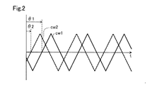
第1インバータ装置211の駆動に用いられる搬送波を「第1搬送波cw1」、第2インバータ装置212の駆動に用いられる搬送波を「第2搬送波をcw2」と呼ぶ。第1実施形態では、図2に示すように、第1搬送波cw1と第2搬送波cw2の周波数は、同一周波数である。ただし、搬送波cw1の周波数と、cw2の周波数は異なる周波数であっても良い。この場合、搬送波cw1の周波数f1と、cw2の周波数f2の比は、整数比であることが好ましい。整数比とは、例えば、f1>f2のとき、f1/f2が整数になることを意味する。第1搬送波cw1の周波数f1と、第2搬送波cw2の周波数f2の比が整数比であれば、第1平滑コンデンサ電流Ic1と第2平滑コンデンサ電流Ic2における搬送波の高次高調波成分が同一周波数となる。このような場合、2つの搬送波cw1、cw2の位相を調整することで、第1平滑コンデンサ電流Ic1と第2平滑コンデンサ電流Ic2の高次高調波成分をキャンセル、あるいは、小さくできる。なお、搬送波cw1、cw2の周波数が同じであれば、第1平滑コンデンサ電流Ic1と第2平滑コンデンサ電流Ic2における搬送波の主要高調波成分をキャンセル、あるいは、小さくできる。
The carrier wave used to drive the
図2に示すように、搬送波cw1、cw2は、三角波である。但し、搬送波cw1、cw2は、正弦波、矩形波、ノコギリ波、台形波など、三角波以外の波形であってもよい。第1搬送波cw1がマイナスからプラスに遷移するゼロクロス点の位相をθ1、代2搬送波cw2がマイナスからプラスに遷移するゼロクロス点の位相をθ2とする。第1平滑コンデンサ電流Ic1と第2平滑コンデンサ電流Ic2を適切な値とするθ1とθ2の値は、直流電源200と、2つのインバータ装置211、212の配置位置により異なる。
As shown in FIG. 2, the carrier waves cw1 and cw2 are triangular waves. However, the carrier waves cw1 and cw2 may have waveforms other than triangular waves such as sine waves, square waves, sawtooth waves, and trapezoidal waves. Let θ1 be the phase of the zero cross point where the first carrier wave cw1 transitions from minus to plus, and θ2 be the phase of the zero cross point where the second carrier wave cw2 transitions from minus to plus. The values of θ1 and θ2 with the first smoothing capacitor current Ic1 and the second smoothing capacitor current Ic2 as appropriate values differ depending on the arrangement positions of the
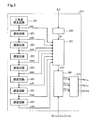
図3に示すように、第1インバータ装置211は、第1三角波発生回路221と、複数の第1遅延回路231と、第1電流比較回路241と、第1搬送波選択回路251と、第1駆動信号生成回路261と、第1H型ブリッジ回路271と、を備える。第1三角波発生回路221は、基準となる三角波cwaを発生する。第1遅延回路231は、入力された三角波を予め定められた位相だけ遅延させる。三角波の1周期を2π、第1遅延回路231の数をn個とすると、1つの第1遅延回路231は、三角波の位相をπ/nだけ遅延させるように設計されている。第1電流比較回路241は、第1平滑コンデンサ電流Ic1と判定値Ithとを比較し、Ic1≧Ithのとき、第1搬送波cw1の位相を遅らせる指示をする信号S1を第1搬送波選択回路251に送る。第1搬送波選択回路251は、選択された搬送波を、第1搬送波cw1として出力する。
As shown in FIG. 3, the
図4に示すように、第1搬送波cw1は、信号S1が入力されるたびに、cwa→cwb→・・・→cwh→/cwa→/cwb→→・・・→/cwh→cwaのように、循環的に位相が遅れる。なお、搬送波/cwaは、搬送波cwaと位相がπだけずれている信号であり、搬送波cwaを図示しないインバータ回路で反転させることで容易に生成できる。また、第1遅延回路231の数を増やして/cwa〜/cwhを第1遅延回路231から生成しても良い。他の搬送波/cwbから/cwhについても同じである。
As shown in FIG. 4, the first carrier wave cw1 is such that each time the signal S1 is input, cwa → cwb → ... → cwh → / cwa → / cwb →→ ... → / cwh → cwa. , The phase is delayed cyclically. The carrier wave / cwa is a signal whose phase is out of phase with the carrier wave cwa by π, and can be easily generated by inverting the carrier wave cwa with an inverter circuit (not shown). Further, the number of the
図3の第1駆動信号生成回路261は、指令信号Cs1u、Cs1v、Cs1wと搬送波cw1とを比較し、第1Hブリッジ回路271を駆動する駆動信号Dr1u、Dr1v、Dr1wを生成する。例えば、第1駆動信号生成回路261は、Cs1u≧Cw1のとき、u相の駆動信号Dr1uをHとし、Cs1u<Cw1のとき、u相の駆動信号Dr1uをLとする。第1駆動信号生成回路261は、他のv相、w相の駆動信号Dr1v、Dr1wについても同様に駆動信号Dr1v、Dr1wを生成する。指令信号Cs1u、Cs1v、Cs1wは、PWM駆動におけるデューティの決定に用いられる。第1Hブリッジ回路271は、駆動信号Dr1u、Dr1v、Dr1wにより、u相、v相、w相の駆動電圧V1u、V1v、V1wを生成する。
The first drive
第2インバータ装置212の構成は、第1インバータ装置211とほぼ同じである。ただし、第2電流比較回路は、第2平滑コンデンサ電流Ic2と判定値Ithとを比較し、Ic2≧Ithのとき、第2搬送波cw2の位相を進ませる指示をする信号を第2搬送波選択回路に送る。第2搬送波選択回路は、選択された搬送波を、第2搬送波cw2として出力する。したがって、図4に示すように、第2搬送波cw2は、信号S2が入力されるたびに、cwh→cwg→・・・cwa→/cwh→/cwg・・・→/cwa→cwhのように、第1搬送波cw1と逆方向に循環的に位相が進む。
The configuration of the
図3に示す例では、第1遅延回路231の数は7個であるが、1つの遅延回路231による遅延量を少なくし、遅延回路231の数を増加させても良い。位相を遅らせる大きさを細かくできるのでより高精度に位相を制御できる。第2インバータ装置212においても同様である。
In the example shown in FIG. 3, the number of the
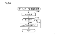
図5Aは、第1インバータ装置221における第1搬送波cw1の位相調整フローチャートである。第1インバータ装置221は、予め定められた期間毎に、この処理を実行する。ステップS100では、第1インバータ装置221は、第1平滑コンデンサ電流Ic1を取得する。ステップS110では、第1インバータ装置221の第1電流比較回路241は、第1平滑コンデンサ電流Ic1と、判定値Ithとを比較し、Ic1>Ithの場合には、信号S1を発信し、ステップS120に移行する。Ic1≦Ithの場合には、処理を終了する。
FIG. 5A is a phase adjustment flowchart of the first carrier wave cw1 in the
ステップS120において、第1インバータ装置211の第1搬送波選択回路251は、信号S1を発信すると、第1搬送波cw1の位相をπ/8だけ遅らせ、その後、処理を終了する。
In step S120, when the first carrier
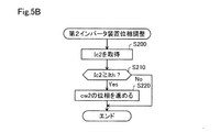
図5Bは、第2インバータ装置222における第2搬送波cw2の位相調整フローチャートである。第2インバータ装置222は、予め定められた期間毎に、この処理を実行する。ステップS200では、第2インバータ装置222は、第2平滑コンデンサ電流Ic2を取得する。ステップS210では、第2インバータ装置222の第2電流比較回路242は、第2平滑コンデンサ電流Ic2と、判定値Ithとを比較し、Ic2>Ithの場合には、信号S2を発信し、ステップS220に移行する。Ic2≦Ithの場合には、処理を終了する。 FIG. 5B is a phase adjustment flowchart of the second carrier wave cw2 in the second inverter device 222. The second inverter device 222 executes this process at predetermined intervals. In step S200, the second inverter device 222 acquires the second smoothing capacitor current Ic2. In step S210, the second current comparison circuit 242 of the second inverter device 222 compares the second smoothing capacitor current Ic2 with the determination value Is, and when Ic2> Is, transmits a signal S2 and steps S220. Move to. When Ic2 ≦ Is, the process ends.
ステップS220において、第2インバータ装置212の第2搬送波選択回路252は、信号S2を発信すると、第2搬送波cw2の位相をπ/8だけ進ませ、その後、処理を終了する。
In step S220, when the second carrier wave selection circuit 252 of the
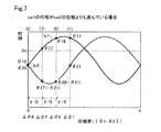
次に、図6A、6Bを用いて、第1搬送波cw1と第2搬送波cw2の位相の調整により第1平滑コンデンサ電流Ic1、第2平滑コンデンサ電流Ic2がどのように変化するか、を説明する。図6Aの横軸は、第1搬送波cw1の位相θ1と第2搬送波cw2の位相θ2との位相差|θ1−θ2|であり、縦軸は、第1平滑コンデンサ電流Ic1と、第2平滑コンデンサ電流Ic2における搬送波cw1、cw2の周波数の2倍の周波数成分である。図6Bは、図6Aの各状態における搬送波cw1、cw2を示す。 Next, with reference to FIGS. 6A and 6B, how the first smoothing capacitor current Ic1 and the second smoothing capacitor current Ic2 change by adjusting the phases of the first carrier wave cw1 and the second carrier wave cw2 will be described. The horizontal axis of FIG. 6A is the phase difference | θ1-θ2 | between the phase θ1 of the first carrier wave cw1 and the phase θ2 of the second carrier wave cw2, and the vertical axis is the first smoothing capacitor current Ic1 and the second smoothing capacitor. It is a frequency component twice the frequency of the carriers cw1 and cw2 in the current Ic2. FIG. 6B shows carriers cw1 and cw2 in each state of FIG. 6A.
初期の状態(1)では、第1搬送波cw1の位相はθ11であり、第2搬送波cw2の位相はθ21であり、位相差Δθ1は、|θ11−θ12|である。状態(1)では、Ic1>Ithであるので、第1インバータ装置211は、第1搬送波cw1の位相をθ11からθ12に遅らせる(図5AのステップS120)。状態(1)では、Ic2≦Ithであるので、第2インバータ装置212は、第2搬送波cw2の位相を進ませない。この処理の結果の状態を状態(2)とする。状態(2)における第1搬送波cw1と第2搬送波cw2の位相差Δθ2(=|θ12−θ22|)は、状態(1)よりもπ/8だけ大きくなっている。したがって、状態(2)における動作点は、状態(1)における動作点よりも右に存在する。状態(2)では、状態(1)と位相差が異なるので、第1平滑コンデンサ電流Ic1、第2平滑コンデンサ電流Ic2が変わる。状態(2)でも同様に、図5A、図5Bに示すフローチャートが実行される。
In the initial state (1), the phase of the first carrier wave cw1 is θ11, the phase of the second carrier wave cw2 is θ21, and the phase difference Δθ1 is | θ11−θ12 |. In the state (1), since Ic1> Is, the
状態(2)では、Ic1>Ithであるので、第1インバータ装置211は、第1搬送波cw1の位相をθ12からθ13に遅らせる(図5AのステップS120)。また、Ic2>Ithであるので、第2インバータ装置212は、第2搬送波cw2の位相をθ22からθ23に進ませる(図5BのステップS220)。この処理の結果の状態を状態(3)とする。状態(3)では、第1搬送波cw1と第2搬送波cw2の位相差Δθ3(=|θ13−θ23|)は、状態(2)よりも大きくなる。なお、状態(1)から状態(2)へは、第1搬送波cw1の位相のみが遅れるのに対し、状態(2)から状態(3)へは、第1搬送波cw1の位相が遅れ、第2搬送波cw2の位相が進む。そのため、状態(3)における第1搬送波cw1と第2搬送波cw2の位相差は、状態(2)よりも2π/8だけ大きくなっている。
In the state (2), since Ic1> Is, the
状態(3)では、Ic1≦Ithであるので、第1インバータ装置211は、第1搬送波cw1の位相を遅らせない。Ic2>Ithであるので、第2インバータ装置212は、第2搬送波cw2の位相をθ23からθ24に進ませる(図5BのステップS220)。この処理の結果の状態を状態(4)とする。状態(4)における第1搬送波cw1と第2搬送波cw2の位相差Δθ4(=|θ14−θ24|)は、状態(3)よりもπ/8だけ大きくなっている。
In the state (3), since Ic1 ≦ Is, the
状態(4)では、Ic1≦Ithであるので、第1インバータ装置211は、第1搬送波cw1の位相を遅らせない。Ic2>Ithであるので、第2インバータ装置212は、第2搬送波cw2の位相をθ24からθ25に進ませる(図5BのステップS220)。この処理の結果の状態を状態(5)とする。状態(5)における第1搬送波cw1と第2搬送波cw2の位相差Δθ5(=|θ15−θ25|)は、状態(4)よりもπ/8だけ大きくなる。
In the state (4), since Ic1 ≦ Is, the
状態(5)では、Ic1≦Ithであるので、第1インバータ装置211は、第1搬送波cw1の位相を遅らせない。Ic2≦Ithであるので、第2インバータ装置212は、第2搬送波cw2の位相を遅らせない。したがって、状態(5)で位相の調整処理が終了する。
In the state (5), since Ic1 ≦ Is, the
図6Aでは、状態(1)で、第1搬送波cw1の位相が第2搬送波cw2の位相よりも遅れている場合を例にとって説明したが、図7に示すように、第1搬送波cw1の位相が第2搬送波cw2の位相よりも進んでいる場合も同様である。 In FIG. 6A, a case where the phase of the first carrier wave cw1 is behind the phase of the second carrier wave cw2 in the state (1) has been described as an example, but as shown in FIG. 7, the phase of the first carrier wave cw1 is The same applies when the phase is ahead of the phase of the second carrier wave cw2.
状態(1)では、第1搬送波cw1の位相はθ11であり、第2搬送波cw2の位相はθ21であり、位相差Δθ1は、|θ11−θ12|である。状態(1)では、Ic1>Ithであるので、第1インバータ装置211は、第1搬送波cw1の位相をθ11からθ12に遅らせる(図5AのステップS120)。状態(1)では、Ic2≦Ithであるので、第2インバータ装置212は、第2搬送波cw2の位相を進ませない。この処理の結果の状態を状態(2)とする。状態(2)における第1搬送波cw1と第2搬送波cw2の位相差Δθ2(=|θ12−θ22|)は、状態(1)よりもπ/8だけ小さくなっている。したがって、状態(2)における動作点は、状態(1)における動作点よりも左に存在する。
In the state (1), the phase of the first carrier wave cw1 is θ11, the phase of the second carrier wave cw2 is θ21, and the phase difference Δθ1 is | θ11−θ12 |. In the state (1), since Ic1> Is, the
以下、説明を省略するが、第1インバータ装置211と第2インバータ装置212は、同様の処理を繰り返すことにより、第8状態(8)となる。第8状態(8)では、Ic1≦Ithとなるので、第1インバータ装置211は、第1搬送波cw1の位相を遅らせない。また、Ic2≦Ithとなるので、第2インバータ装置212は、第2搬送波cw2の位相を進ませない。このように、第1搬送波cw1と第2搬送波cw2の位相の初期位置にかかわらず、位相の調整が可能である。
Hereinafter, although description will be omitted, the
以上、本実施形態によれば、第1インバータ装置211は、第1インバータ装置211接続される第1平滑コンデンサC1に流れる第1平滑コンデンサ電流Ic1が判定値Ithを超えた場合には、第1インバータ装置211に供給される第1搬送波cw1の位相遅らせる(図5AのステップS120)。また、第2インバータ装置212は、第2インバータ装置212に接続される第2平滑コンデンサC2に流れる第2平滑コンデンサ電流Ic2が判定値Ithを超えた場合には、第2搬送波cw2の位相を進ませる(図5BのステップS220)。その結果、インバータ装置211、212の配置位置によらず、第1搬送波cw1と第2搬送波cw2の位相差を適切に調整し、平滑コンデンサ電流Ic1、Ic2を低減することができる。
As described above, according to the present embodiment, the
上記実施形態では、各インバータ装置211、212は、自己に接続される平滑コンデンサの電流のみに基づいて、それぞれ搬送波cw1、cw2の位相を遅らせ、進ませる。したがって、第1インバータ装置211と、第1インバータ装置212との間の通信が不要である。また、通信の遅れによる影響も発生しない。
In the above embodiment, the
上記実施形態では、2つのインバータ装置211、212は、いずれも三相変調インバータ装置であるとしたが、2つのインバータ装置211、212が二相変調インバータ装置であってもよい。なお、判定値Ithと比較する平滑コンデンサ電流Ic1、Ic2は、2つのインバータ装置211、212が三相変調インバータ装置の場合には、搬送波cw1、cw2の周波数の2倍の第2次高調波成分であることが好ましく、2つのインバータ装置211、212が二相変調インバータ装置の場合には、搬送波cw1、cw2の周波数成分であることが好ましい。
In the above embodiment, the two
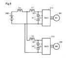
・第2実施形態:
図8に示す第2実施形態では、2つのインバータ装置のうちの一方の第1インバータ装置211は、三相変調インバータ装置であるが、他方の第2インバータ装置215は、二相変調インバータ装置である。この場合であっても、同様に、第1平滑コンデンサ電流Ic1が判定値Ithを超えた場合には、第1インバータ装置211は、第1搬送波cw1の位相を遅らせ(図5AのステップS120)、第2平滑コンデンサ電流Ic5が判定値Ithを超えた場合には、第2インバータ装置215は、第2搬送波cw5の位相を進ませる(図5BのステップS220)。したがって、第1実施形態と同様に、インバータ装置211、212の配置位置によらず、第1搬送波cw1と第2搬送波cw2の位相差を適切に調整し、平滑コンデンサ電流Ic1、Ic2を低減することができる。なお、第2実施形態では、二相変調インバータ装置である第2インバータ装置215の第2搬送波cw5の周波数f5は、三相変調インバータ装置である第1インバータ装置211の第1搬送波cw1の周波数f1の2倍であることが好ましい。第1平滑コンデンサ電流Ic1、第2平滑コンデンサ電流の主要な高調波成分をキャンセルできる。
-Second embodiment:
In the second embodiment shown in FIG. 8, one of the two inverter devices, the
・第3実施形態:
図9に示す第3実施形態では、4つのインバータ装置211〜214と、4つの電動モータ301〜304を備える。第3インバータ装置213には、第3平滑コンデンサC3が接続され、第4インバータ装置214には、第4平滑コンデンサC4が接続されている。図9のLbは、直流電源200から、2つのインバータ装置213、214の分岐点N2までの配線インダクタであり、L3は、分岐点N2から第3インバータ装置213までの配線インダクタであり、L4は、分岐点N2から第4インバータ装置214までの配線インダクタである。
-Third embodiment:
The third embodiment shown in FIG. 9 includes four
第3実施形態では、2つのインバータ装置をペアとして、ペアにおける2つの搬送波の位相を調整する。以下、どのような2つのインバータ装置をペアとするかについて説明する。具体的には、2つの平滑コンデンサの距離が近い2つのインバータ装置をペアとする。このペアは、2つの平滑コンデンサの間の配線インダクタを求めることで決定できる。例えば、第1平滑コンデンサC1と第2平滑コンデンサC2との間の配線インダクタの大きさは、L1+L2である。第1平滑コンデンサC1と第3平滑コンデンサC3との間の配線インダクタの大きさは、L1+La+Lb+L3であり、第1平滑コンデンサC1と第4平滑コンデンサC4との間の配線インダクタの大きさは、L1+La+Lb+L4である。L1+L2<L1+La+Lb+L3、L1+L2<L1+La+Lb+L4である。したがって、第1平滑コンデンサC1にとって、第2平滑コンデンサC2までにインダクタの大きさが最も小さく、距離が最も近い。したがって、第1インバータ装置211と、第2インバータ装置212とがペアとなる。同様に、第3インバータ装置213と、第4インバータ装置214とがペアとなる。一般に、2つの平滑コンデンサの距離が最も近いペアとなる2つのインバータ装置は、相互の影響が強い。その2つのインバータ装置をペアとして、その搬送波の位相を調整すれば、平滑コンデンサ電流を低減できる。
In the third embodiment, two inverter devices are paired and the phases of the two carrier waves in the pair are adjusted. Hereinafter, what kind of two inverter devices are paired will be described. Specifically, two inverter devices in which the distance between the two smoothing capacitors is close are paired. This pair can be determined by finding the wiring inductor between the two smoothing capacitors. For example, the size of the wiring inductor between the first smoothing capacitor C1 and the second smoothing capacitor C2 is L1 + L2. The size of the wiring inductor between the first smoothing capacitor C1 and the third smoothing capacitor C3 is L1 + La + Lb + L3, and the size of the wiring inductor between the first smoothing capacitor C1 and the fourth smoothing capacitor C4 is L1 + La + Lb + L4. is there. L1 + L2 <L1 + La + Lb + L3, L1 + L2 <L1 + La + Lb + L4. Therefore, for the first smoothing capacitor C1, the size of the inductor is the smallest and the distance is the shortest by the second smoothing capacitor C2. Therefore, the
上記、各実施形態において、インバータ装置211、212がそれぞれ三角波発生回路221、222を備えているが、搬送波cw1、cw2の周波数が同一周波数の場合には、三角波発生回路をインバータ装置211、212と別に設け、搬送波cwaを各インバータ装置211、212に入力するように構成しても良い。
In each of the above embodiments, the
上記実施形態において、遅延回路231、232をそれぞれ7個設け、1回分の搬送波cw1の位相を遅らせる大きさと、1回分の搬送波cw2の位相を進ませる大きさとを、いずれも2π/8として、同じ大きさとしているが、インバータ装置211、212とで、遅延回路の231、232の数を変えて、1回分の搬送波cw1の位相を遅らせる大きさΔφ1と、1回分の搬送波cw2の位相を進ませる大きさΔφ2とを異なる大きさとしても良い。
In the above embodiment, seven
上記実施形態において、搬送波cw2の波形は、2πごとに同じ波形となるため、第2インバータ装置212は、位相をΔφ2進ませる代わりに、位相を(2π−Δφ2)遅らせてもよい。第1インバータ装置211が位相Δφ2を遅らせる場合も同様に、位相を(2π−Δφ1)進めても良い。
In the above embodiment, since the waveform of the carrier wave cw2 is the same every 2π, the
本開示は、上述の実施形態に限られるものではなく、その趣旨を逸脱しない範囲において種々の構成で実現することができる。例えば、発明の概要の欄に記載した各形態中の技術的特徴に対応する実施形態の技術的特徴は、上述の課題の一部又は全部を解決するために、あるいは、上述の効果の一部又は全部を達成するために、適宜、差し替えや、組み合わせを行うことが可能である。また、その技術的特徴が本明細書中に必須なものとして説明されていなければ、適宜、削除することが可能である。 The present disclosure is not limited to the above-described embodiment, and can be realized by various configurations within a range not deviating from the gist thereof. For example, the technical features of the embodiments corresponding to the technical features in each embodiment described in the column of the outline of the invention are for solving a part or all of the above-mentioned problems, or a part of the above-mentioned effects. Or, in order to achieve all of them, it is possible to replace or combine them as appropriate. Further, if the technical feature is not described as essential in the present specification, it can be appropriately deleted.
200 直流電源 211、212インバータ装置 281、282 電流センサ C1、C2 平滑コンデンサ cw1、cw2 搬送波 Ic1、Ic2 平滑コンデンサ電流 Ith 電流の判定値
200
Claims (8)
前記直流電源にそれぞれ平滑コンデンサを介して接続される2つのインバータ装置(211、212)と、
前記平滑コンデンサの電流をそれぞれ取得する2つの電流センサ(281、282)と、
を備え、
前記2つのインバータ装置のうちの第1インバータ装置(211)は、第1平滑コンデンサ(C1)に流れる第1平滑コンデンサ電流(Ic1)が判定値(Ith)を超えた場合に前記第1インバータ装置の駆動に用いられる第1搬送波(cw1)の位相を遅らせ、
前記2つのインバータ装置のうちの前記第1インバータ装置と異なる第2インバータ装置(211)は、第2平滑コンデンサ(C2)に流れる第2平滑コンデンサ電流(Ic2)が判定値(Ith)を超えた場合に前記第2インバータ装置の駆動に用いられる第2搬送波(cw2)の位相を進ませる、
電力供給装置。 DC power supply (200) and
Two inverter devices (211 and 212) connected to the DC power supply via smoothing capacitors, respectively.
Two current sensors (281 and 282) that acquire the current of the smoothing capacitor, respectively, and
With
The first inverter device (211) of the two inverter devices is the first inverter device when the first smoothing capacitor current (Ic1) flowing through the first smoothing capacitor (C1) exceeds the determination value (Ith). Delay the phase of the first carrier wave (cw1) used to drive the
In the second inverter device (211), which is different from the first inverter device among the two inverter devices, the second smoothing capacitor current (Ic2) flowing through the second smoothing capacitor (C2) exceeds the determination value (Ith). In some cases, the phase of the second carrier (cw2) used for driving the second inverter device is advanced.
Power supply device.
前記第1搬送波の周波数と前記第2搬送波の周波数の比は、整数である、電力供給装置。 The power supply device according to claim 1.
A power supply device in which the ratio of the frequency of the first carrier wave to the frequency of the second carrier wave is an integer.
前記第1インバータ装置及び前記第2インバータ装置は、いずれも三相変調インバータ装置であり、
前記第1搬送波の周波数と前記第2搬送波の周波数は同一周波数である、電力供給装置。 The power supply device according to claim 2.
The first inverter device and the second inverter device are both three-phase modulation inverter devices.
A power supply device in which the frequency of the first carrier wave and the frequency of the second carrier wave are the same frequency.
前記第1平滑コンデンサ電流における前記第1搬送波の第2次高調波成分を前記判定値と比較し、
前記第2平滑コンデンサ電流における前記第2搬送波の第2次高調波成分を前記判定値と比較する、電力供給装置。 The power supply device according to claim 3.
The second harmonic component of the first carrier wave in the first smoothing capacitor current is compared with the determination value.
A power supply device that compares the second harmonic component of the second carrier wave in the second smoothing capacitor current with the determination value.
前記第1インバータ装置及び前記第2インバータ装置は、いずれも二相変調インバータ装置であり、
前記第1搬送波の周波数と前記第2搬送波の周波数は同一周波数である、電力供給装置。 The power supply device according to claim 2.
The first inverter device and the second inverter device are both two-phase modulation inverter devices.
A power supply device in which the frequency of the first carrier wave and the frequency of the second carrier wave are the same frequency.
前記第1平滑コンデンサ電流における前記第1搬送波の周波数成分を前記判定値と比較し、用い、
前記第2平滑コンデンサ電流における前記第2搬送波の周波数成分を前記判定値と比較する、電力供給装置。 The power supply device according to claim 5.
The frequency component of the first carrier wave in the first smoothing capacitor current is compared with the determination value and used.
A power supply device that compares the frequency component of the second carrier wave in the second smoothing capacitor current with the determination value.
前記第1インバータ装置と前記第2インバータ装置のうちの一方は二相変調インバータ装置であり、
前記第1インバータ装置と前記第2インバータ装置のうちの他方は三相変調インバータ装置であり、
前記二相変調インバータ装置の搬送波の周波数は、前記前記三相変調インバータ装置の搬送波の周波数の2倍である、電力供給装置。 The power supply device according to claim 2.
One of the first inverter device and the second inverter device is a two-phase modulation inverter device.
The other of the first inverter device and the second inverter device is a three-phase modulation inverter device.
A power supply device in which the frequency of the carrier wave of the two-phase modulation inverter device is twice the frequency of the carrier wave of the three-phase modulation inverter device.
前記直流電源には2の2倍以上のインバータ装置が接続され、
それぞれ接続される前記第1平滑コンデンサと前記第2平滑コンデンサとの距離が最も近い組み合わせとなる2つのインバータ装置を前記第1インバータ装置と前記第2インバータ装置として前記第1搬送波と前記第2搬送波が制御される、電力供給装置。 The power supply device according to any one of claims 1 to 7.
An inverter device that is more than twice as large as 2 is connected to the DC power supply.
The first carrier wave and the second carrier wave are two inverter devices having the closest combination of the first smoothing capacitor and the second smoothing capacitor to be connected as the first inverter device and the second inverter device. Is controlled by a power supply device.
Priority Applications (1)
| Application Number | Priority Date | Filing Date | Title |
|---|---|---|---|
| JP2019088745A JP2020184846A (en) | 2019-05-09 | 2019-05-09 | Power supplying device |
Applications Claiming Priority (1)
| Application Number | Priority Date | Filing Date | Title |
|---|---|---|---|
| JP2019088745A JP2020184846A (en) | 2019-05-09 | 2019-05-09 | Power supplying device |
Publications (1)
| Publication Number | Publication Date |
|---|---|
| JP2020184846A true JP2020184846A (en) | 2020-11-12 |
Family
ID=73044705
Family Applications (1)
| Application Number | Title | Priority Date | Filing Date |
|---|---|---|---|
| JP2019088745A Pending JP2020184846A (en) | 2019-05-09 | 2019-05-09 | Power supplying device |
Country Status (1)
| Country | Link |
|---|---|
| JP (1) | JP2020184846A (en) |
Cited By (3)
| Publication number | Priority date | Publication date | Assignee | Title |
|---|---|---|---|---|
| WO2023286197A1 (en) * | 2021-07-14 | 2023-01-19 | 三菱電機株式会社 | Power conversion device |
| WO2023144952A1 (en) * | 2022-01-27 | 2023-08-03 | 株式会社日立製作所 | Inverter apparatus and inverter control method |
| EP4607777A1 (en) * | 2024-02-21 | 2025-08-27 | Wobben Properties GmbH | Method for feeding electric power into an electric network by means of an inverter having a plurality of parallel connected sub-inverters |
-
2019
- 2019-05-09 JP JP2019088745A patent/JP2020184846A/en active Pending
Cited By (6)
| Publication number | Priority date | Publication date | Assignee | Title |
|---|---|---|---|---|
| WO2023286197A1 (en) * | 2021-07-14 | 2023-01-19 | 三菱電機株式会社 | Power conversion device |
| JPWO2023286197A1 (en) * | 2021-07-14 | 2023-01-19 | ||
| JP7466779B2 (en) | 2021-07-14 | 2024-04-12 | 三菱電機株式会社 | Power Conversion Equipment |
| WO2023144952A1 (en) * | 2022-01-27 | 2023-08-03 | 株式会社日立製作所 | Inverter apparatus and inverter control method |
| JP7667320B2 (en) | 2022-01-27 | 2025-04-22 | 株式会社日立製作所 | Inverter device and inverter control method |
| EP4607777A1 (en) * | 2024-02-21 | 2025-08-27 | Wobben Properties GmbH | Method for feeding electric power into an electric network by means of an inverter having a plurality of parallel connected sub-inverters |
Similar Documents
| Publication | Publication Date | Title |
|---|---|---|
| US6594164B2 (en) | PWM controlled power conversion device | |
| US10594220B2 (en) | Power supply device and method for controlling power supply device | |
| CN107425758B (en) | Method and system for controlling a motor control device | |
| EP1921740A2 (en) | Power converter control | |
| JP5466830B2 (en) | Multi-phase motor drive | |
| JP5593362B2 (en) | Multi-phase motor drive | |
| US10250171B2 (en) | Electric motor control apparatus and electric motor control method | |
| JP2011078251A (en) | Apparatus for controlling electric motor drive device | |
| JP2020184846A (en) | Power supplying device | |
| JP2019103266A (en) | Control device for multiple-coil rotary machine | |
| JP2008109727A (en) | Inverter device | |
| US7426122B2 (en) | Power-converter control apparatus employing pulse width modulation and adjusting duration of a zero-voltage vector | |
| WO2017145841A1 (en) | Inverter control device | |
| JP2020080627A (en) | Power conversion device and power conversion method thereof | |
| JP5593361B2 (en) | Multi-phase motor drive | |
| JPWO2020044890A1 (en) | Inverter device | |
| JP2019201444A (en) | Inverter controller and inverter control method | |
| US9019734B2 (en) | Solid state switch gate firing with phase shift delay line | |
| JP4063185B2 (en) | Power supply | |
| JP4410769B2 (en) | Power conversion system for AC train vehicles | |
| JPH02168895A (en) | Method of decreasing peak current value of voltage-type pulse width modulation control inverter | |
| JP6868927B1 (en) | 3-pulse PWM control method for three-phase inverter | |
| RU2319283C2 (en) | Method of feeding synchronous hysteresis motor with overexcitation | |
| JP3182322B2 (en) | PWM control device for NPC inverter | |
| JP2017051013A (en) | Motor control device |