JP2020055152A - Droplet discharge device and image formation method - Google Patents
Droplet discharge device and image formation method Download PDFInfo
- Publication number
- JP2020055152A JP2020055152A JP2018185888A JP2018185888A JP2020055152A JP 2020055152 A JP2020055152 A JP 2020055152A JP 2018185888 A JP2018185888 A JP 2018185888A JP 2018185888 A JP2018185888 A JP 2018185888A JP 2020055152 A JP2020055152 A JP 2020055152A
- Authority
- JP
- Japan
- Prior art keywords
- power supply
- selection information
- circuit
- waveform signal
- drive
- Prior art date
- Legal status (The legal status is an assumption and is not a legal conclusion. Google has not performed a legal analysis and makes no representation as to the accuracy of the status listed.)
- Granted
Links
Images


Landscapes
- Ink Jet (AREA)
- Particle Formation And Scattering Control In Inkjet Printers (AREA)
Abstract
【課題】制御回路と駆動回路とを接続する配線数を削減でき、かつ良好な画質が得られる液滴吐出装置及び画像形成方法を提供する。
【解決手段】液滴吐出装置は、ノズルに対応する駆動素子をN個有するヘッドと、電源回路21〜25と、電源選択情報に従って各駆動素子に接続する電源回路を選択するN個の電源回路セレクタ、及び波形信号選択情報に従って各駆動素子に出力する波形信号を選択するN個の波形信号セレクタを備え、波形信号に従って駆動素子の駆動を行う駆動回路27と、画像データに基づいて駆動素子毎に、前記電源選択情報及び波形信号選択情報を決定し、これらを一つの信号線33を介して駆動回路27にシリアル伝送する制御回路51とを備える。制御回路51は、前記電源選択情報を駆動回路27へ伝送した後、前記画像データの受信が終了するまでの間に、前記電源選択情報を駆動回路27へ再送する。
【選択図】図3An object of the present invention is to provide a droplet discharge device and an image forming method capable of reducing the number of wirings for connecting a control circuit and a drive circuit and obtaining good image quality.
A droplet discharge device includes a head having N drive elements corresponding to nozzles, power supply circuits 21 to 25, and N power supply circuits for selecting a power supply circuit connected to each drive element according to power supply selection information. A driving circuit 27 for driving the driving element according to the waveform signal, comprising a selector and N number of waveform signal selectors for selecting a waveform signal to be output to each driving element according to the waveform signal selection information; And a control circuit 51 for determining the power supply selection information and the waveform signal selection information, and serially transmitting these to the drive circuit 27 via one signal line 33. After transmitting the power supply selection information to the drive circuit 27, the control circuit 51 retransmits the power supply selection information to the drive circuit 27 until the reception of the image data ends.
[Selection diagram] FIG.
Description
本技術は、ノズルから液体、例えばインクを吐出する液滴吐出装置及び画像形成方法に関する。 The present technology relates to a droplet discharge device that discharges a liquid, for example, ink from a nozzle, and an image forming method.
従来、複数のノズルからインクを吐出する液滴吐出装置が開示されている。液滴吐出装置は、各ノズルに対応する各圧電素子に駆動信号を供給するか否かを規定する吐出データと、各圧電素子に供給する駆動信号の種類を規定するCOM選択データとを記憶する描画データメモリを備える。 Conventionally, a droplet discharge device that discharges ink from a plurality of nozzles has been disclosed. The droplet discharge device stores discharge data that specifies whether to supply a drive signal to each piezoelectric element corresponding to each nozzle, and COM selection data that specifies the type of drive signal to be supplied to each piezoelectric element. It has a drawing data memory.
COM選択データは、駆動電圧の波高値及び波形を含む。描画データメモリからCOM選択回路にCOM選択データが送られ、各圧電素子を駆動する為の電圧の波高値及び波形が選択される。また描画データメモリからスイッチング回路に吐出データが送られ、スイッチング回路は、吐出データに基づいて、所定の圧電素子に駆動信号を供給する。駆動信号を供給された圧電素子は、選択された電圧の波高値及び波形によって、駆動される。 The COM selection data includes the peak value and the waveform of the drive voltage. COM selection data is sent from the drawing data memory to the COM selection circuit, and a peak value and a waveform of a voltage for driving each piezoelectric element are selected. Further, ejection data is sent from the drawing data memory to the switching circuit, and the switching circuit supplies a drive signal to a predetermined piezoelectric element based on the ejection data. The piezoelectric element to which the drive signal has been supplied is driven by the peak value and waveform of the selected voltage.
描画データメモリと、COM選択回路及びスイッチング回路とは、複数の配線によって接続されており、回路の構成が複雑になっている。
本願発明者は、回路の構成を簡素化するために、描画データメモリと、COM選択回路及びスイッチング回路とを、例えば1つの配線によって接続することを考えた。この場合、1つの配線を介して、COM選択データ及び吐出データが送られることになる。COM選択データ又は吐出データをCOM選択回路又はスイッチング回路に入力するために、COM選択データ及び吐出データのヘッダ部分にいずれのデータであるかを識別する識別データを付与させる。しかし、静電気等のノイズによって識別データの内容が変わってしまうと、適切なデータがスイッチング回路に入力されない虞がある。この場合、画素毎に指定するドットのサイズに対応して液滴がノズルから吐出されず、画質が悪くなることがある。
The drawing data memory, the COM selection circuit, and the switching circuit are connected by a plurality of wirings, and the circuit configuration is complicated.
The inventor of the present application has considered that the drawing data memory, the COM selection circuit and the switching circuit are connected by, for example, one wiring in order to simplify the circuit configuration. In this case, the COM selection data and the ejection data are sent through one wiring. In order to input the COM selection data or the ejection data to the COM selection circuit or the switching circuit, identification data for identifying the data is added to the header of the COM selection data and the ejection data. However, if the content of the identification data changes due to noise such as static electricity, there is a possibility that appropriate data may not be input to the switching circuit. In this case, the droplets are not ejected from the nozzles corresponding to the dot size specified for each pixel, and the image quality may be degraded.
本開示は斯かる事情に鑑みてなされたものであり、制御回路と駆動回路とを接続する配線数を削減でき、かつ良好な画質が得られる液滴吐出装置及び画像形成方法を提供することを目的とする。 The present disclosure has been made in view of such circumstances, and it is an object of the present disclosure to provide a droplet discharge apparatus and an image forming method which can reduce the number of wirings for connecting a control circuit and a drive circuit and can obtain good image quality. Aim.
本開示に係る液滴吐出装置は、N個のノズルにそれぞれ対応する駆動素子をN個有するヘッドと、複数の電源回路と、前記複数の電源回路の中から、N個の電源選択情報に従って各駆動素子に接続する電源回路を選択する、N個の電源回路セレクタ、及びN個の波形信号選択情報に従って各駆動素子に出力する波形信号を選択する、N個の波形信号セレクタを備え、選択した前記波形信号に従ってN個の駆動素子の駆動を行う駆動回路と、画素毎に形成するドットサイズを指定する複数のドットサイズデータで構成された画像データを受信し、前記画像データに基づいて、前記駆動素子毎に、前記電源選択情報及び前記波形信号選択情報を決定し、決定した前記電源選択情報及び前記波形信号選択情報を一つの信号線を介して前記駆動回路にシリアル伝送する制御回路とを備え、前記制御回路は、前記電源選択情報を前記駆動回路へ伝送した後、前記画像データの受信が終了するまでの間に、前記電源選択情報を前記駆動回路へ再送する。 The droplet discharge device according to the present disclosure includes a head having N driving elements respectively corresponding to the N nozzles, a plurality of power supply circuits, and each of the plurality of power supply circuits according to N power supply selection information. N power supply circuit selectors for selecting a power supply circuit to be connected to the drive element, and N waveform signal selectors for selecting a waveform signal to be output to each drive element according to the N waveform signal selection information are selected. A drive circuit that drives the N drive elements according to the waveform signal, and receives image data composed of a plurality of dot size data specifying a dot size to be formed for each pixel, and based on the image data, For each drive element, the power supply selection information and the waveform signal selection information are determined, and the determined power supply selection information and the waveform signal selection information are transmitted to the drive circuit via one signal line. A control circuit for performing real transmission, wherein after transmitting the power supply selection information to the drive circuit, the control circuit retransmits the power supply selection information to the drive circuit until reception of the image data ends. I do.
本開示に係る液滴吐出装置にあっては、制御回路は、N個の波形信号選択情報及びN個の電源選択情報を一つの信号線を介して駆動回路にシリアル伝送するので、制御回路と駆動回路とを接続する配線数を削減することができる。
そして、印刷中に、駆動素子に接続する電源回路を選択する電源選択情報を再送するので、ノイズ等が生じて駆動素子が異なる電源回路に接続されている場合に、適切な電源回路に接続し直すことができ、良好な画質が得られる。
In the droplet discharge device according to the present disclosure, the control circuit serially transmits the N pieces of waveform signal selection information and the N pieces of power supply selection information to the drive circuit via one signal line. The number of wirings for connecting to the driving circuit can be reduced.
Then, during printing, the power supply selection information for selecting the power supply circuit to be connected to the drive element is retransmitted. Therefore, when noise or the like is generated and the drive element is connected to a different power supply circuit, the power supply is connected to an appropriate power supply circuit. Can be corrected, and good image quality can be obtained.
実施の形態1.
以下本発明を実施の形態1に係る印刷装置1を示す図面に基づいて説明する。図1は、印刷装置1を示す平面図である。印刷装置1は、例えば、インクジェットプリンタである。なお、図1に示すように、便宜上、本明細書において、前後左右それぞれの方向を矢印で示す方向として説明する。印刷装置1は筐体2を備える。
Hereinafter, the present invention will be described with reference to the drawings showing a
筐体2には、プラテン3、4個のインクジェットヘッド4、及び搬送ローラ5、6などが備えられている。なお、インクジェットヘッド4、搬送ローラ5、6の数は図1の例に限定されない。
The
また、筐体2には、複数のヘッド保持部8が取り付けられている。複数のヘッド保持部8は、プラテン3の上方で、且つ、二つの搬送ローラ5、6の間の位置において、前後方向に沿って並設されている。ヘッド保持部8によって、インクジェットヘッド4がそれぞれ保持される。
The
プラテン3上には、印刷装置1で用いる記録媒体100が載置される。搬送ローラ5、6は、プラテン3の前後方向の両端部に配置され、記録媒体100は、搬送ローラ5、6が回転することによって、前後方向(搬送方向)に沿って搬送される。
A
インクジェットヘッド4は、平面視において外形が矩形状をなす。インクジェットヘッド4は、記録媒体100が搬送される搬送方向(前後方向)が短手となり、搬送方向と直交する方向(左右方向)が長手となるように配置されている。インクジェットヘッド4は、インクジェットヘッドのノズル面がプラテン3に対向するように配置されている。4つの各インクジェットヘッド4は、前後方向に沿って搬送ローラ5、6間に並んでいる。
The outer shape of the
4つのインクジェットヘッド4はそれぞれ、例えば、シアン、マゼンタ、イエロー、ブラックに対応する。
The four
インクジェットヘッド4は、複数の液滴吐出装置としてのヘッドユニット11を備える。また、ヘッドユニット11は、後述の基板50、後述のフレキシブル回路基板60を備える。基板50には、フレキシブル回路基板60が接続される。すなわち、基板50とフレキシブル回路基板60とは、それぞれ一つのヘッドユニット11に対応して一つ設けられる。例えば、印刷装置1が4個のインクジェットヘッド4を備え、各インクジェットヘッド4が9個のヘッドユニット11を備える場合、印刷装置1は、36個のヘッドユニット11を備えるので、基板50は36個となり、基板50と接続されたフレキシブル回路基板60も36個となる。
The
印刷装置1は制御部(不図示)を有し、制御部はモータ(不図示)を作動させて、搬送ローラ5、6の動作を制御して、記録媒体100の搬送を行う。外部装置9(例えばパーソナルコンピュータ)は、印刷指示の信号や印刷する画像のラスターデータ(画像データ)等を後述の基板50へ送信する。外部装置9は、ユーザの操作を受け付ける受付部としても機能する。印刷装置1は、記録媒体100の搬送中に各インクジェットヘッド4のヘッドユニット11から、記録媒体100に向けてインクを吐出させる。
The
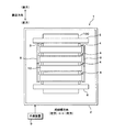
図2は本実施の形態のインクジェットヘッド4をノズル面側から見た場合の要部構成の一例を示す平面図である。ヘッドユニット11は、前後方向に2列で配置されている。前側の列82では、左右方向に沿って4個のヘッドユニット11が配置され、後側の列81では、左右方向に沿って5個のヘッドユニット11が配置されている。ヘッドユニット11のノズル面(ノズルプレートの下面)には、n個のノズルの吐出口(開口)11aが設けられている。また、ヘッドユニット11にはノズルの吐出口11aと同数(つまり、n個)の駆動素子111(後述)が設けられている。なお、ノズルの吐出口11aは、便宜上模式的に表しており、実際の配置及び個数とは異なる。また、図2の例では、インクジェットヘッド4が、9個のヘッドユニット11を備える構成であるが、ヘッドユニット11の数は9個に限定されない。各ヘッドユニット11は、後述の基板50、フレキシブル回路基板60などを備える。
FIG. 2 is a plan view showing an example of a main configuration of the
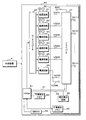
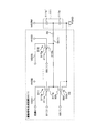
図3は本実施の形態のヘッドユニット11が備える基板50と、基板50と接続されたフレキシブル回路基板60との構成の一例を示すブロック図である。図3では、一つの基板50と一つのフレキシブル回路基板60とを図示する。
FIG. 3 is a block diagram showing an example of the configuration of the
基板50は、コントローラとしてのFPGA51、EEPROMなどの不揮発性メモリ52、外部装置9から受信したラスターデータを一時的に格納するDRAM53、D/Aコンバータ20、電源回路21、電源回路22、電源回路23、電源回路24、電源回路25、電源回路26などを備える。また、フレキシブル回路基板60は、EEPROMなどの不揮発性メモリ62、ドライバIC27などを備える。なお、FPGA51に代えてCPU(Central Processing Unit )又はMPU(Microprocessor Unit )などの制御用のICを使用してもよい。
The
FPGA51は、電源回路21〜電源回路26の出力電圧を設定する設定信号をD/Aコンバータ20へ出力する。D/Aコンバータ20は、FPGA51が出力するデジタルの設定信号をアナログの設定信号に変換して電源回路21〜電源回路26に出力する。
The
電源回路21〜電源回路26は、例えば、FET、インダクタ、抵抗、電解コンデンサ等の複数の電子部品で構成されるDC/DCコンバータとすることができる。各電源回路21〜26は、設定信号で指定された、出力電圧をドライバIC27に出力する。
The
電源回路21〜25は、配線VDD1〜VDD5を介してドライバIC27と接続されている。電源回路26は配線HVDDを介してドライバIC27と接続されている。なお、電源回路26は、後述の駆動素子111と配線VCOMを介して接続されている。配線HVDDと配線VCOMは、電源回路26から引き出された配線が、経路の途中で2つの配線に分岐したものである。
The
電源回路21〜電源回路26は、ドライバIC27の内部に形成された駆動信号生成回路30(1)〜駆動信号生成回路30(n)(nは2以上の自然数であり、例えば、ヘッドユニット11が有する駆動素子111の数に等しい)にそれぞれ接続されている。ドライバIC27の詳細は後述する。
The
電源回路21〜電源回路25は、通常使用する電源回路である。また、電源回路26は、特別仕様の電源回路である。電源回路26は、駆動素子111のVCOM用電源電圧として併用すること、あるいは後述のPMOSトランジスタ311〜315のHVDD(ハイサイド側バッグゲート電圧)として使用することができる。電源回路21〜電源回路25の電圧の大小関係は、例えば、電源回路21の電圧<電源回路22の電圧<電源回路23の電圧<電源回路24の電圧<電源回路25の電圧である。
電源回路21〜電源回路25には、それぞれ電圧センサV及び電流センサIが接続されている。なお、電源回路21〜電源回路25には、電圧センサV及び電流センサIのいずれかを接続することにしてもよい。
The
A voltage sensor V and a current sensor I are connected to the
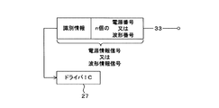
ドライバIC27は、1本の制御線33を介してFPGA51と接続されている。また、ドライバIC27はn本の信号線34(1)〜(n)を介して、n個の駆動素子111とそれぞれ接続されている。各信号線34は、駆動素子の個別電極と接続されている。また、ドライバIC27はグランド線である配線GNDと接続されている。
The
制御線33には、ドライバIC27が有する後述のn個の電源回路セレクタ90(1)〜(n)を制御するための電源情報信号と、後述のn個の波形信号セレクタ91(1)〜(n)を制御するための波形情報信号とが伝送される。電源情報信号には、n個の電源選択情報としてn個の電源番号に関する情報の信号が含まれる。また、波形情報信号には、n個の波形信号選択情報としてn個の波形番号に関する情報の信号が含まれる。また、FPGA51は、n個の電源選択情報に従ってn個の電源回路セレクタ90(1)〜(n)を制御し、n個の波形信号選択情報に従ってn個の波形信号セレクタ91(1)〜(n)を制御することで、各信号線34に出力する駆動信号を生成するための電源回路及び波形信号を選択する。
制御線33には、電圧を検出する電圧検出回路36が接続されている。
The
A
また、ドライバIC27は、制御線31を介してFPGA51と接続されている。ドライバIC27は、後述する波形信号(0)〜(6)を生成する波形信号生成回路200を備えている。波形信号生成回路200は、制御線31を介して受信する制御信号に従って、波形信号(0)〜(6)の波形信号を生成する。なお、制御線31は複数本備えられており、波形信号生成回路200は複数本の制御線31から受信する複数種類の制御信号に従って、波形信号(0)〜(6)を生成するものであってもよい。
The
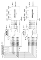
図4は、ドライバIC27が備える回路構成の一例を示すブロック図である。図5は、制御線33に伝送される電源情報信号及び波形情報信号を示す概念図である。
図4に示すように、ドライバIC27は波形信号生成回路200を備える。波形信号生成回路200は、制御線31から受信した制御信号に従って、互いに異なる7つの波形信号(0)〜(6)の波形信号を生成する。波形信号(0)〜(6)は、駆動信号生成回路30が備えるトランジスタを制御するパルス信号である。各波形信号(0)〜(6)は、互いにパルスの幅またはパルスの数などが異なっている。波形信号生成回路により生成された各波形信号(0)〜(6)は、それぞれn個の電源回路セレクタ90(1)〜(n)に供給される。
FIG. 4 is a block diagram illustrating an example of a circuit configuration included in the
As shown in FIG. 4, the
図4に示すように、ドライバIC27は、n個の識別回路92(1)〜92(n)を備える。n個の識別回路92(1)〜92(n)は、n個の電源回路セレクタ90(1)〜(n)にそれぞれ接続されている。またn個の識別回路92(1)〜92(n)は、n個の波形信号セレクタ91(1)〜(n)にそれぞれ接続されている。n個の波形信号セレクタ91(1)〜(n)は、n個の電源回路セレクタ90(1)〜(n)にそれぞれ接続されている。n個の電源回路セレクタ90(1)〜(n)は、n個の駆動信号生成回路30(1)〜駆動信号生成回路30(n)にそれぞれ接続されている。FPGA51からの1本の制御線33は分岐し、n個の識別回路92(1)〜92(n)に接続されている。
As shown in FIG. 4, the
n個の電源回路セレクタ90(1)〜(n)は、n個の駆動素子111に対応して設けられている。n個の波形信号セレクタ91(1)〜(n)は、n個の駆動素子111に対応して設けられている。各電源回路セレクタ90及び各波形信号セレクタ91は、ドライバIC27の内部に形成された複数のFETなどから構成されるハードウェアの構成要素である。
The n power supply circuit selectors 90 (1) to 90 (n) are provided corresponding to the
ドライバIC27は、同様の構成をノズルの数と同じ数のn個分備えているので、以下では、代表して、電源回路セレクタ90(1)と、波形信号セレクタ91(1)と、信号線34(1)との間に備えられた回路構成について説明する。電源回路セレクタ90(1)及び波形信号セレクタ91(1)の間から分岐した制御線SB(1)は、駆動信号生成回路30(1)に接続されている。
Since the
電源回路セレクタ90(1)と駆動信号生成回路30(1)とは、5本の制御線S1(1)、S2(1)、S3(1)、S4(1)、及びS5(1)で接続されている。電源回路セレクタ90(1)は、電源情報信号に従って、5本の制御線S1(1)、S2(1)、S3(1)、S4(1)、及びS5(1)の中から選択されるいずれか一つの制御線を、波形信号セレクタ91(1)と接続する。5本の制御線S1(1)、S2(1)、S3(1)、S4(1)、及びS5(1)は、5個の電源回路21〜25にそれぞれ対応する。
The power supply circuit selector 90 (1) and the drive signal generation circuit 30 (1) are connected to five control lines S1 (1), S2 (1), S3 (1), S4 (1), and S5 (1). It is connected. The power supply circuit selector 90 (1) is selected from five control lines S1 (1), S2 (1), S3 (1), S4 (1), and S5 (1) according to the power supply information signal. One of the control lines is connected to the waveform signal selector 91 (1). The five control lines S1 (1), S2 (1), S3 (1), S4 (1), and S5 (1) correspond to the five
また、駆動信号生成回路30(1)には、上述の配線VDD1〜5と接続される5つの配線と、配線HVDDと接続される配線と、配線GNDと接続される配線とが接続されている。 Further, the drive signal generation circuit 30 (1) is connected to five wires connected to the above-described wires VDD1 to 5, a wire connected to the wire HVDD, and a wire connected to the wire GND. .
n個の各電源回路セレクタ90(1)〜(n)は、5個の電源回路21〜25のいずれかを選択することができる。n個の各波形信号セレクタ91(1)〜(n)に、7個の波形信号(0)〜波形信号(6)全てが入力されている。各波形信号セレクタ91(1)〜(n)は、7個の波形信号(0)〜波形信号(6)のいずれかを選択することができる。
Each of the n power supply circuit selectors 90 (1) to 90 (n) can select any one of the five
図5に示すように、制御線33には、電源情報信号又は波形情報信号がシリアル伝送される。電源情報信号は、識別情報と、n個の電源番号を指定するための情報である電源選択情報とを有する。また、波形情報信号は、識別情報と、n個の波形番号を指定するための情報である波形信号選択情報とを有する。
As shown in FIG. 5, a power supply information signal or a waveform information signal is serially transmitted to the
識別情報は、電源情報信号であるのか、波形情報信号であるのかを識別するための情報である。例えば、識別回路92(1)〜(n)は、識別情報がハイレベルを示す場合、電源情報信号であると判定し、識別情報がローレベルを示す場合、波形情報信号であると判定する。 The identification information is information for identifying whether the signal is a power supply information signal or a waveform information signal. For example, the identification circuits 92 (1) to 92 (n) determine that the identification information is a power supply information signal when the identification information indicates a high level, and determine that the identification information is a waveform information signal when the identification information indicates a low level.
電源情報信号に含まれる電源番号は、電源回路21〜25のいずれかを識別する番号であって、電源選択情報の一例である。本実施例では、電源番号1〜5はそれぞれ電源回路21〜25を示す。FPGA51は、外部装置9から吐出開始命令を受信したとき、電源情報信号をドライバIC27に送る。識別回路92(1)〜(n)は電源番号を確認し、電源回路セレクタ90(1)〜(n)に、電源回路21〜25のいずれかを選択させる。
The power supply number included in the power supply information signal is a number for identifying one of the
波形情報信号に含まれる波形番号は、7個の波形信号(0)〜波形信号(6)のいずれかを識別する番号であって、波形信号選択情報の一例である。FPGA51は、電源情報信号をドライバIC27に送った後、画像データを波形信号選択情報に変換し、波形情報信号をドライバIC27に送る。識別回路92(1)〜(n)は、波形番号を確認し、波形信号セレクタ91(1)〜(n)に、波形信号(0)〜波形信号(6)のいずれかを選択させる。なお波形信号(0)は、不吐出時に使用する波形である。
The waveform number included in the waveform information signal is a number for identifying any one of the seven waveform signals (0) to (6), and is an example of waveform signal selection information. After sending the power supply information signal to the
不揮発性メモリ52には、各ドットサイズデータに対応する波形番号と電源番号との組み合わせの関係を示すデータが記憶されている。ドットサイズデータは、画素ごとに形成するドットのサイズを指定するデータである。1個の画素は1個の駆動素子111に対応する。外部装置9から受信した画像データは各駆動素子111に対応する複数のドットサイズデータを含む。駆動素子111の駆動によって、後述するように吐出口11aからドットサイズデータに対応する液滴量のインクが吐出される。
The
図6は、ドライバIC27が備える駆動信号生成回路30(1)の構成の一例を示す回路図である。なお、駆動信号生成回路30(1)〜(n)は、同様の構成をなすので、図6では、駆動信号生成回路30(1)について説明する。駆動信号生成回路30(1)は、5つのPMOS(P-type Metal Oxide Semiconductor)トランジスタ311〜315(図5では、2つのみ図示)、一つのNMOS(N-type Metal Oxide Semiconductor)トランジスタ32、抵抗35などを備える。駆動信号生成回路30(1)は、信号線34(1)を介して、駆動素子111の個別電極と接続されている。
FIG. 6 is a circuit diagram illustrating an example of a configuration of the drive signal generation circuit 30 (1) included in the
本実施の形態の駆動素子111は、特開2015−24531(特願2013−154357)の図5に開示されているような圧電素子である。駆動素子111は、個別電極と第1の定電位電極との間に挟まれる第1活性部と、個別電極と第2の定電位電極との間に挟まれる第2活性部とを備える圧電素子である。このため、駆動素子111は、キャパシタ111bと、キャパシタ111b′とを備える。
The driving
信号線34(1)には、5つのPMOSトランジスタ311〜315の5つのソース端子311a〜315aが接続されている。NMOSトランジスタ32のソース端子32aは、グランドに接続されている。なお、図6においては、PMOSトランジスタ312〜314の図示を省略している。
The signal line 34 (1) is connected to five
また、PMOSトランジスタ311〜315のゲート端子311c〜315cにはそれぞれ、制御線S1(1)〜S5(1)が接続されている。また、NMOSトランジスタ32のゲート端子32cには、制御線SB(1)が接続されている。
Control lines S1 (1) to S5 (1) are connected to
また、PMOSトランジスタ311〜315は、配線VDD1〜VDD5を介して電源回路21〜25と接続されている。
The
また、5つのPMOSトランジスタ311〜315のドレイン端子311b〜315bは、抵抗35の一端に接続されている。また、NMOSトランジスタ32のドレイン端子32bは、抵抗35の一端に接続されている。抵抗35の他端は、駆動素子111の個別電極(キャパシタ111b′の他端及びキャパシタ111bの一端)に接続されている。駆動素子111の第1の定電位電極(キャパシタ111b′の一端)はVCOMに接続され、駆動素子111の第2の定電位電極(キャパシタ111bの他端)はグラウンドに接続されている。
The
波形信号セレクタ91(1)から、ハイレベル(「H」)の信号が電源回路セレクタ90(1)に出力されると、電源回路セレクタ90(1)で選択された信号線と接続されたPMOSトランジスタ311〜315のいずれか一つのPMOSトランジスタはオン状態となる。電源回路21〜25のいずれか一つから供給される電圧によってキャパシタ111bが充電され、キャパシタ111b′が放電される。一方、波形信号セレクタ91(1)から、ローレベル(「L」)の信号が電源回路セレクタ90(1)に出力されると、NMOSトランジスタ32はオン状態となり、電源回路21〜25のうちのいずれか一つから出力される電圧によってキャパシタ111b′が充電され、キャパシタ111bが放電される。キャパシタ111b、111b′が交互に充電及び放電を行うことによって、駆動素子111は変形し、ノズルの吐出口11aからインクが吐出される。
When a high-level (“H”) signal is output from the waveform signal selector 91 (1) to the power supply circuit selector 90 (1), the PMOS connected to the signal line selected by the power supply circuit selector 90 (1) Any one of the
すなわち、信号線34(1)には駆動素子111を駆動する駆動信号が出力される。電源回路セレクタ90(1)が、接続する制御線を5つの制御線S1(1)〜S5(1)のうちからいずれか一つを選択することで、駆動信号を生成する電源回路を5つの電源回路21〜25の中から選択することができる。
That is, a drive signal for driving the
以下、本実施の形態のヘッドユニット11の動作について説明する。
ヘッドユニット11のFPGA51は、外部装置9から吐出開始命令を受信したとき、電源情報信号をドライバIC27に送る。FPGA51は、例えば各ノズルの吐出口11aから均一に液滴を吐出できるように、各駆動素子111に接続する電源回路を選択する。ドライバIC27は、電源選択情報に従って、電源回路セレクタ90により、各駆動素子111を電源選択情報で指定されたいずれかの電源回路に接続する。
その後、FPGA51は、外部装置9から画像データを受信すると、画像データを波形信号選択情報に変換し、波形信号選択情報をドライバIC27に送る。ドライバIC27は、波形信号選択情報に従って、波形信号セレクタ91により、駆動素子111毎に波形信号選択情報で指定されたいずれかの波形信号を選択する。
Hereinafter, the operation of the
The
Thereafter, when receiving the image data from the
波形信号セレクタ91にて選択された波形信号は、電源回路セレクタ90にて選択された電源回路によって、所定の電圧を印加され、駆動信号生成回路30に入力される。駆動素子111は、入力された波形信号によって定められるパルス幅やパルス数、及び選択された電源回路の出力電圧によって定められる波高値の駆動信号に基づいて駆動され、ノズルの吐出口11aから、ドットサイズデータに対応した液滴量のインクが吐出され、記録媒体100に画像が形成される。
FPGA51は、画像データを受信し続けるので、FPGA51は、一度、電源情報信号を送った後は、ドライバIC27に、波形信号情報を送り続けることになる。
The waveform signal selected by the
Since the
電源情報と波形情報とは同じフォーマットである。
ドライバIC27が波形信号選択情報を保持している状態で、静電気等のノイズが発生し、識別情報がローレベルからハイレベルになったとき、本来は、波形信号選択情報としての意味を有していた情報が、電源選択情報とされる場合がある。この場合、ドライバIC27は、各駆動素子111を、当初の電源選択情報で選択された電源回路とは異なる電源回路に接続する。FPGA51は、電源選択情報を、画像データを受信している間には送らないため、各駆動素子111が不適切な電源回路に接続され、各ノズルから吐出される液滴が当初設定した大きさとは異なる大きさとなり、画質が悪化する。
The power supply information and the waveform information have the same format.
When noise such as static electricity is generated while the
そこで、電源情報信号を、印刷中に再送する。
電源情報信号の再送は、例えば画像データとして、1ライン分の画素がないデータを受信した場合、異常を検知した場合等に行う。
1ラインとは、記録媒体100の搬送方向に直交する方向に並ぶ、先頭画素から最終画素までの画素群をいう。1ライン分の画素がない空白データを受信した場合、印刷画像に影響を与えることなく、電源情報信号を送ることができる。
異常は、波形信号選択情報に基づいて推定される各電源回路の電圧又は電流値と、電圧センサV又は電流センサIにより実測した各電源回路の電圧又は電流値とに基づいて検知する。また、異常は、制御線33に接続した電圧検出回路36により検出した電圧に基づいて検知してもよい。
Therefore, the power supply information signal is retransmitted during printing.
The retransmission of the power supply information signal is performed, for example, when data having no pixels for one line is received as image data, or when an abnormality is detected.
One line refers to a group of pixels from the first pixel to the last pixel arranged in a direction orthogonal to the transport direction of the
The abnormality is detected based on the voltage or current value of each power supply circuit estimated based on the waveform signal selection information and the voltage or current value of each power supply circuit actually measured by the voltage sensor V or the current sensor I. Further, the abnormality may be detected based on the voltage detected by the
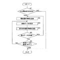
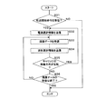
図7は、FPGA51による電源情報送信処理を示すフローチャートである。
FPGA51は、以下の電源情報送信処理を適宜の間隔で行う。
FPGA51は、外部装置9から吐出開始命令を受信したか否かを判定する(S1)。FPGA51は吐出開始命令を受信していないと判定した場合(S1:NO)、電源情報送信処理を終了する。
FPGA51は吐出開始命令を受信したと判定した場合(S1:YES)、ドライバIC27に電源情報信号を送信し、電源選択情報を送る(S2)。ドライバIC27は、電源選択情報に従って、電源回路セレクタ90により、各駆動素子111をそれぞれ指定された電源回路に接続する。
FIG. 7 is a flowchart illustrating the power information transmission process by the
The
The
When determining that the
FPGA51は、外部装置9から画像データを受信する(S3)。
FPGA51は画像データに従って、駆動素子111毎に波形信号を決定し、波形情報信号をドライバIC27に送信し、波形信号選択情報を送る(S4)。ドライバIC27は、波形信号選択情報に従って、波形信号セレクタ91により、駆動素子111毎に波形を選択し、選択された波形に従って、駆動素子111を駆動する。これにより各駆動素子111に対応した各ノズルの吐出口11aからインクが吐出される。
The
The
FPGA51は、空白データ(1ライン分の画素がないデータ)を受信したか否かを判定する(S5)。FPGA51は空白データを受信したと判定した場合(S5:YES)、処理をS2へ戻す。
The
FPGA51は空白データを受信していないと判定した場合(S5:NO)、画像データの受信が終了したか否かを判定する(S6)。FPGA51は、複数のライン分につき空白データを受信した場合、又は印刷終了データを受信した場合等に、画像データの受信が終了したと判定する。
FPGA51は画像データの受信が終了していないと判定した場合(S6:NO)、処理をS3へ戻す。
FPGA51は画像データの受信が終了したと判定した場合(S6:YES)、電源情報送信処理を終了する。
When determining that the blank data has not been received (S5: NO), the
If the
When the
空白データを受信した場合、印刷画像に影響を与えることなく、ドライバIC27に電源情報信号を再送することができる。
そして、当初の電源選択情報により選択された電源回路に駆動素子111を接続することができるので、各ノズルの吐出口11aから吐出される液滴が画像データに基づき設定したドットサイズとなり、良好な画質が得られる。
When the blank data is received, the power supply information signal can be retransmitted to the
Then, since the
(変形例1)
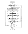
図8は、FPGA512による変形例1の電源情報送信処理を示すフローチャートである。
FPGA51は、以下の電源情報送信処理を適宜の間隔で行う。
FPGA51は、外部装置9から吐出開始命令を受信したか否かを判定する(S11)。FPGA51は吐出開始命令を受信していないと判定した場合(S11:NO)、電源情報送信処理を終了する。
FPGA51は吐出開始命令を受信したと判定した場合(S11:YES)、ドライバIC27に電源情報信号を送信し、電源選択情報を送る(S12)。ドライバIC27は、電源選択情報に従って、電源回路セレクタ90により、各駆動素子111をそれぞれ指定された電源回路に接続する。
(Modification 1)
FIG. 8 is a flowchart illustrating a power supply information transmission process according to the first modification by the FPGA 512.
The
The
When determining that the
FPGA51は、外部装置9から画像データを受信する(S13)。
FPGA51は画像データに従って、駆動素子111毎に波形信号を決定し、波形情報信号をドライバIC27に送信し、波形信号選択情報を送る(S14)。ドライバIC27は、波形信号選択情報に従って、波形信号セレクタ91により、駆動素子111毎に波形を選択し、選択された波形に従って、駆動素子111を駆動する。これにより各駆動素子111に対応した各ノズルの吐出口11aからインクが吐出される。
The
The
FPGA51は、電源選択情報及び波形信号選択情報に従って、各電源回路の電圧又は電流値を推定する(S15)。
FPGA51は、各電源回路の電圧又は電流値を電圧センサV又は電流センサIにより取得する(S16)。
The
The
FPGA51は、電圧又は電流値の推定値と実測値との差の絶対値が閾値a以下であるか否かを判定する(S17)。電圧の前記絶対値がa以上である場合、複数の電源回路のうち、特定の電源回路に集中して複数の駆動素子111が接続されていることになり、異常が発生していることが検知される。また、各電源回路の推定の電流低下量と実測の電流低下量との差の絶対値がa以上である場合も、同様に異常が発生していることが検知される。
FPGA51は、前記絶対値がa以下でないと判定した場合(S17:NO)、処理をS12へ戻す。
The
If the
FPGA51は、前記絶対値がa以下であると判定した場合(S17:YES)、画像データの受信が終了したか否かを判定する(S18)。FPGA51は画像データの受信が終了していないと判定した場合(S18:NO)、処理をS13へ戻す。
FPGA51は画像データの受信が終了したと判定した場合(S18:YES)、電源情報送信処理を終了する。
When determining that the absolute value is equal to or smaller than a (S17: YES), the
When the
変形例1の場合、異常を検知した場合、即時に電源選択情報を再送するので、画質の悪化を直ちに抑制することができる。
電源選択情報の再送により、当初の電源選択情報により選択された電源回路に駆動素子111を接続することができるので、各ノズルの吐出口11aから吐出される液滴が画像データに基づき設定したドットサイズとなり、以後、良好な画質が得られる。
In the case of the first modification, when an abnormality is detected, the power supply selection information is immediately retransmitted, so that the deterioration of the image quality can be suppressed immediately.
By retransmitting the power supply selection information, the driving
(変形例2)
図9は、FPGA512による変形例2の電源情報送信処理を示すフローチャートである。
FPGA51は、以下の電源情報送信処理を適宜の間隔で行う。
FPGA51は、外部装置9から吐出開始命令を受信したか否かを判定する(S21)。FPGA51は吐出開始命令を受信していないと判定した場合(S21:NO)、電源情報送信処理を終了する。
FPGA51は吐出開始命令を受信したと判定した場合(S21:YES)、ドライバIC27に電源情報信号を送信し、電源選択情報を送る(S22)。ドライバIC27は、電源選択情報に従って、電源回路セレクタ90により、各駆動素子111をそれぞれ指定された電源回路に接続する。
(Modification 2)
FIG. 9 is a flowchart illustrating a power supply information transmission process according to the second modification by the FPGA 512.
The
The
When determining that the
FPGA51は、外部装置9から画像データを受信する(S23)。
FPGA51は画像データに従って、駆動素子111毎に波形信号を決定し、波形情報信号をドライバIC27に送信し、波形信号選択情報を送る(S24)。ドライバIC27は、波形信号選択情報に従って、波形信号セレクタ91により、駆動素子111毎に波形を選択し、選択された波形に従って、駆動素子111を駆動する。これにより、各駆動素子111に対応した各ノズルの吐出口11aからインクが吐出される。
The
The
FPGA51は、電圧検出回路36が検出した制御線33の電圧が閾値b以下であるか否かを判定する(S25)。ノイズの一例として、静電気が発生した場合、制御線33の電圧が高くなる。電圧が閾値b以下であるか否かを判定することにより、異常を検知できる。
FPGA51は電圧が閾値b以下でないと判定した場合(S25:NO)、処理をS22へ戻す。
FPGA51は電圧が閾値b以下であると判定した場合(S25:YES)、画像データの受信が終了したか否かを判定する(S26)。FPGA51は画像データの受信が終了していないと判定した場合(S26:NO)、処理をS23へ戻す。
FPGA51は画像データの受信が終了したと判定した場合(S26:YES)、電源情報送信処理を終了する。
The
If the
When determining that the voltage is equal to or lower than the threshold value b (S25: YES), the
If the
変形例2の場合、異常を検知した場合、即時に電源選択情報を再送するので、画質の悪化を直ちに抑制することができる。
電源選択情報の再送により、当初の電源選択情報により選択された電源回路に駆動素子111を接続することができるので、各ノズルの吐出口11aから吐出される液滴が画像データに基づき設定したドットサイズとなり、以後、良好な画質が得られる。
In the case of the second modification, when an abnormality is detected, the power supply selection information is immediately retransmitted, so that the deterioration of the image quality can be suppressed immediately.
By retransmitting the power supply selection information, the driving
実施の形態2.
以下、実施の形態2に係る印刷装置1について説明する。図10は、印刷装置1を示す概略斜視図である。実施の形態2に係る印刷装置1は、記録媒体100の移動方向に交差する方向(走査方向、図10における左方向及び右方向に沿う方向)に、インクジェットヘッドが移動するスキャン方式の印刷装置である。インクジェットヘッドが移動すること以外は、実施の形態1に係る印刷装置1と同様の構成を有する。
Hereinafter, the
図10に示すように、印刷装置1は、キャリッジ14と、インクジェットヘッド16と、記録媒体100を搬送させる図示しない搬送機構と、キャリッジ14を案内するガイドレール19と、キャリッジ14を移動させる図示しない移動機構とを備えている。インクジェットヘッド16は、キャリッジ14に設けられている。移動機構は、ベルトと、モータと、該モータの回転角度及び回転方向を検出するエンコーダ15とを備える。キャリッジ14は、ベルトを介してモータと接続されている。モータを駆動させると、キャリッジ14がガイドレール19に沿って走査方向に移動する。FPGA51には、エンコーダ15から出力されるパルス信号が入力される。FPGA51は、エンコーダ15からのパルス信号に基づいて、モータの回転速度及び回転量を算出し、モータを制御する。エンコーダ15は2相のパルス信号を出力する構成となっており、FPGA51は、この2相のパルス信号のオンオフの順番に応じて、キャリッジ14の移動方向を判定する。
As shown in FIG. 10, the
インクジェットヘッド16は、複数のインクタンク17と、複数のヘッドユニット18とを有している。ヘッドユニット18は、インクを記録媒体100に対して吐出する。印刷装置1は複数の色のインクを利用するようになっており、夫々の色についてインクタンク17及びヘッドユニット18が備えられている。例えば、印刷装置1は、シアン(C)、マゼンタ(M)、イエロー(Y)及びブラック(K)の4色のインクを利用し、インクジェットヘッド16は4個のインクタンク17及び4個のヘッドユニット18を有している。インクジェットヘッド16の左側から順に、ブラック(K)のインクタンク17、イエロー(Y)のインクタンク17、シアン(C)のインクタンク17、及びマゼンタ(M)のインクタンク17が配置されている。インクタンク17とヘッドユニット18とは1対1に対応しており、インクタンク17からは対応するヘッドユニット18へインクが供給される。ヘッドユニット18は、実施の形態1と同様に、ノズル面を有し、該ノズル面には、複数のノズルの吐出口11aが設けられている。各駆動素子111は、各吐出口11aに対応する。
The
不揮発性メモリ52には、各ドットサイズデータに対応する波形番号と電源番号との組み合わせの関係を示すデータが記憶されている。ドットサイズデータは、画素ごとに形成するドットのサイズを指定するデータである。1個の画素は1個の駆動素子111に対応する。外部装置9から受信した画像データは各駆動素子111に対応する複数のドットサイズデータを含む。駆動素子111の駆動によって、吐出口11aからドットサイズデータに対応する量のインクが吐出される。
The
以下、本実施の形態のヘッドユニット18の動作について説明する。
ヘッドユニット18のFPGA51は、外部装置9から吐出開始命令を受信したとき、電源情報信号をドライバIC27に送る。FPGA51は、例えば各ノズルの吐出口11aから均一に液滴を吐出できるように、各駆動素子111に接続する電源回路を選択する。ドライバIC27は、電源選択情報に従って、電源回路セレクタ90により、各駆動素子111を電源選択情報で指定されたいずれかの電源回路に接続する。
その後、FPGA51は、外部装置9から画像データを受信すると、画像データを波形信号選択情報に変換し、波形信号選択情報をドライバIC27に送る。ドライバIC27は、波形信号選択情報に従って、波形信号セレクタ91により、駆動素子111毎に波形信号選択情報で指定されたいずれかの波形を選択する。
波形信号セレクタ91にて選択された波形信号は、電源回路セレクタ90にて選択された電源回路によって、所定の電圧を印加され、駆動信号生成回路30に入力される。駆動素子111は、入力された波形信号によって定められるパルス幅やパルス数、及び選択された電源回路の出力電圧によって定められる波高値の駆動信号に基づいて駆動され、ノズルの吐出口11aから、ドットサイズデータに対応した液滴量のインクが吐出され、記録媒体100に画像が形成される。
FPGA51は、画像データを受信し続けるので、FPGA51は、一度、電源情報信号を送った後は、ドライバIC27に、波形信号情報を送り続ける。
Hereinafter, the operation of the
The
Thereafter, when receiving the image data from the
The waveform signal selected by the
Since the
ドライバIC27が波形信号選択情報を保持している状態で、静電気等のノイズが発生し、識別情報がローレベルからハイレベルになったとき、波形信号選択情報の内容が、電源選択情報の内容とされる場合がある。この場合、ドライバIC27は、各駆動素子111を、当初の電源選択情報で選択された電源回路とは異なる電源回路に接続してしまう。FPGA51は、電源選択情報を、画像データを受信している間は送らないため、各駆動素子111が不適切な電源回路に接続され、各ノズルから吐出される液滴が当初設定した大きさとは異なる大きさとなり、画質が悪化する。
When noise such as static electricity is generated while the
そこで、FPGA51は、電源情報信号を印刷中に再送する。
図11は、FPGA512による電源情報送信処理を示すフローチャートである。
FPGA51は、以下の電源情報送信処理を適宜の間隔で行う。
FPGA51は、外部装置9から吐出開始命令を受信したか否かを判定する(S31)。FPGA51は吐出開始命令を受信していないと判定した場合(S31:NO)、電源情報送信処理を終了する。
FPGA51は吐出開始命令を受信したと判定した場合(S31:YES)、ドライバIC27に電源情報信号を送信し、電源選択情報を送る(S32)。ドライバIC27は、電源選択情報に従って、電源回路セレクタ90により、各駆動素子111をそれぞれ指定された電源回路に接続する。
Therefore, the
FIG. 11 is a flowchart illustrating power supply information transmission processing by the FPGA 512.
The
The
When determining that the ejection start command has been received (S31: YES), the
FPGA51は、外部装置9から画像データを受信する(S33)。
FPGA51は画像データに従って、駆動素子111毎に波形信号を決定し、波形情報信号をドライバIC27に送信し、波形信号選択情報を送る(S34)。ドライバIC27は、波形信号選択情報に従って、波形信号セレクタ91により、駆動素子111毎に波形を選択し、選択された波形に従って、駆動素子111を駆動する。これにより、各駆動素子111に対応した各ノズルの吐出口11aからインクが吐出される。
The
The
FPGA51は、キャリッジ14の移動方向が反転したか否かを判定する(S35)。FPGA51は、2相のパルス信号のオンオフの順番に応じて、キャリッジ14の移動方向を判定する。また、FPGA51は、パルス信号の数の積算値により、キャリッジ14が記録媒体100の端部の外側にあるか否かを判定し、キャリッジ14の移動方向が反転したか否かを判定することにしてもよい。
FPGA51はキャリッジ14の移動方向が反転したと判定した場合(S35:YES)、処理をS32へ戻す。
FPGA51はキャリッジ14の移動方向が反転していないと判定した場合(S35:NO)、画像データの受信が終了したか否かを判定する(S36)。FPGA51は画像データの受信が終了していないと判定した場合(S36:NO)、処理をS33へ戻す。
FPGA51は画像データの受信が終了したと判定した場合(S36:YES)、電源情報送信処理を終了する。
The
When determining that the moving direction of the
When determining that the moving direction of the
If the
キャリッジ14が反転する場合、インクの吐出が休止するので、このタイミングで電源選択情報を再送することにより、印刷に影響を与えることなく、当初の電源選択情報で選択された電源回路に駆動素子111を接続することができる。従って、各ノズルの吐出口11aから吐出される液滴が画像データに基づき設定したドットサイズとなり、良好な画質が得られる。
When the
本実施の形態においても、実施の形態1と同様に、空白のデータを受信したとき、電圧センサV又は電流センサIにより電源回路の接続の異常を検知したとき、及び電圧検出回路36により制御線33におけるノイズの発生等の異常を検知したとき、電源選択情報を再送することにしてもよい。
Also in the present embodiment, similarly to the first embodiment, when blank data is received, when the voltage sensor V or the current sensor I detects an abnormality in the connection of the power supply circuit, and when the
今回開示した実施の形態は、全ての点で例示であって、制限的なものではないと考えられるべきである。各実施例にて記載されている技術的特徴は互いに組み合わせることができ、本発明の範囲は、特許請求の範囲内での全ての変更及び特許請求の範囲と均等の範囲が含まれることが意図される。 The embodiment disclosed this time is an example in all respects, and should be considered as not being restrictive. The technical features described in each embodiment can be combined with each other, and the scope of the present invention is intended to include all the modifications within the scope of the claims and the scope equivalent to the scope of the claims. Is done.
11、18 ヘッドユニット(ヘッド)
11a 吐出口
14 キャリッジ
21〜26 電源回路
27 ドライバIC(駆動回路)
33 制御線(信号線)
36 電圧検出回路
51 FPGA(制御回路)
V 電圧センサ
I 電流センサ
11, 18 Head unit (head)
33 Control line (signal line)
36
V voltage sensor I current sensor
Claims (7)
複数の電源回路と、
前記複数の電源回路の中から、N個の電源選択情報に従って各駆動素子に接続する電源回路を選択する、N個の電源回路セレクタ、及び
N個の波形信号選択情報に従って各駆動素子に出力する波形信号を選択する、N個の波形信号セレクタを備え、選択した前記波形信号に従ってN個の駆動素子の駆動を行う駆動回路と、
画素毎に形成するドットサイズを指定する複数のドットサイズデータで構成された画像データを受信し、
前記画像データに基づいて、前記駆動素子毎に、前記電源選択情報及び前記波形信号選択情報を決定し、
決定した前記電源選択情報及び前記波形信号選択情報を一つの信号線を介して前記駆動回路にシリアル伝送する制御回路と
を備え、
前記制御回路は、
前記電源選択情報を前記駆動回路へ伝送した後、
前記画像データの受信が終了するまでの間に、前記電源選択情報を前記駆動回路へ再送する、液滴吐出装置。 A head having N driving elements respectively corresponding to the N nozzles,
Multiple power circuits,
N power supply circuit selectors for selecting a power supply circuit to be connected to each drive element according to N power supply selection information from among the plurality of power supply circuits, and output to each drive element according to N waveform signal selection information A drive circuit comprising: N waveform signal selectors for selecting a waveform signal; and driving the N drive elements according to the selected waveform signal;
Receiving image data composed of a plurality of dot size data specifying a dot size to be formed for each pixel,
Based on the image data, for each of the drive elements, determine the power supply selection information and the waveform signal selection information,
A control circuit for serially transmitting the determined power supply selection information and the determined waveform signal selection information to the drive circuit via one signal line,
The control circuit includes:
After transmitting the power supply selection information to the drive circuit,
A droplet discharge device that retransmits the power supply selection information to the drive circuit until the reception of the image data ends.
前記制御回路は、前記キャリッジの移動方向が反転したときに再送する、請求項1に記載の液滴吐出装置。 A carriage for reciprocating the head in a scanning direction,
2. The droplet discharge device according to claim 1, wherein the control circuit resends when the moving direction of the carriage is reversed.
前記異常は、前記検出回路が検出した電圧に基づいて検知される、請求項4に記載の液滴吐出装置。 A detection circuit that detects a voltage of the signal line,
The droplet discharge device according to claim 4, wherein the abnormality is detected based on a voltage detected by the detection circuit.
N個のノズルにそれぞれ対応するN個の駆動素子毎に、各駆動素子に接続する電源回路を夫々選択するN個の電源選択情報を決定し、
前記駆動素子を駆動する駆動回路へ前記電源選択情報をシリアル伝送し、
該電源選択情報に基づいて各駆動素子を電源回路に接続し、
前記画像データに基づいて、前記駆動素子毎に、各駆動素子に出力する波形信号を選択するN個の波形信号選択情報を決定し、
前記波形信号選択情報を前記駆動回路にシリアル伝送し、
各駆動素子に出力する波形信号を選択し、
前記画像データの受信が終了するまでの間に、前記電源選択情報を前記駆動回路へ再送し、
画像を形成する画像形成方法。
Receiving image data composed of a plurality of dot size data specifying a dot size to be formed for each pixel,
For each of the N driving elements corresponding to the N nozzles, N power selection information for selecting a power supply circuit connected to each driving element is determined,
Serially transmitting the power supply selection information to a drive circuit that drives the drive element,
Connecting each drive element to a power supply circuit based on the power supply selection information;
Based on the image data, N pieces of waveform signal selection information for selecting a waveform signal to be output to each drive element are determined for each drive element,
Serially transmitting the waveform signal selection information to the drive circuit,
Select the waveform signal to be output to each drive element,
Until the reception of the image data ends, retransmit the power supply selection information to the drive circuit,
An image forming method for forming an image.
Priority Applications (1)
| Application Number | Priority Date | Filing Date | Title |
|---|---|---|---|
| JP2018185888A JP7135684B2 (en) | 2018-09-28 | 2018-09-28 | Droplet ejection device and image forming method |
Applications Claiming Priority (1)
| Application Number | Priority Date | Filing Date | Title |
|---|---|---|---|
| JP2018185888A JP7135684B2 (en) | 2018-09-28 | 2018-09-28 | Droplet ejection device and image forming method |
Publications (2)
| Publication Number | Publication Date |
|---|---|
| JP2020055152A true JP2020055152A (en) | 2020-04-09 |
| JP7135684B2 JP7135684B2 (en) | 2022-09-13 |
Family
ID=70106012
Family Applications (1)
| Application Number | Title | Priority Date | Filing Date |
|---|---|---|---|
| JP2018185888A Active JP7135684B2 (en) | 2018-09-28 | 2018-09-28 | Droplet ejection device and image forming method |
Country Status (1)
| Country | Link |
|---|---|
| JP (1) | JP7135684B2 (en) |
Cited By (1)
| Publication number | Priority date | Publication date | Assignee | Title |
|---|---|---|---|---|
| CN114347654A (en) * | 2020-10-13 | 2022-04-15 | 精工电子打印科技有限公司 | Liquid ejecting head and liquid ejecting recording apparatus |
Citations (6)
| Publication number | Priority date | Publication date | Assignee | Title |
|---|---|---|---|---|
| US6027195A (en) * | 1996-11-12 | 2000-02-22 | Varis Corporation | System and method for synchronizing the piezoelectric clock sources of a plurality of ink jet printheads |
| JP2006205521A (en) * | 2005-01-27 | 2006-08-10 | Fuji Xerox Co Ltd | Liquid droplet ejection device |
| JP2006272905A (en) * | 2005-03-30 | 2006-10-12 | Seiko Epson Corp | Liquid ejection device |
| JP2008188889A (en) * | 2007-02-05 | 2008-08-21 | Fuji Xerox Co Ltd | Driving circuit of capacitive load and image forming apparatus |
| JP2017177755A (en) * | 2016-03-31 | 2017-10-05 | ブラザー工業株式会社 | Control circuit, inkjet head system, and control method |
| JP2019177676A (en) * | 2018-03-30 | 2019-10-17 | ブラザー工業株式会社 | Droplet discharge device |
-
2018
- 2018-09-28 JP JP2018185888A patent/JP7135684B2/en active Active
Patent Citations (6)
| Publication number | Priority date | Publication date | Assignee | Title |
|---|---|---|---|---|
| US6027195A (en) * | 1996-11-12 | 2000-02-22 | Varis Corporation | System and method for synchronizing the piezoelectric clock sources of a plurality of ink jet printheads |
| JP2006205521A (en) * | 2005-01-27 | 2006-08-10 | Fuji Xerox Co Ltd | Liquid droplet ejection device |
| JP2006272905A (en) * | 2005-03-30 | 2006-10-12 | Seiko Epson Corp | Liquid ejection device |
| JP2008188889A (en) * | 2007-02-05 | 2008-08-21 | Fuji Xerox Co Ltd | Driving circuit of capacitive load and image forming apparatus |
| JP2017177755A (en) * | 2016-03-31 | 2017-10-05 | ブラザー工業株式会社 | Control circuit, inkjet head system, and control method |
| JP2019177676A (en) * | 2018-03-30 | 2019-10-17 | ブラザー工業株式会社 | Droplet discharge device |
Cited By (1)
| Publication number | Priority date | Publication date | Assignee | Title |
|---|---|---|---|---|
| CN114347654A (en) * | 2020-10-13 | 2022-04-15 | 精工电子打印科技有限公司 | Liquid ejecting head and liquid ejecting recording apparatus |
Also Published As
| Publication number | Publication date |
|---|---|
| JP7135684B2 (en) | 2022-09-13 |
Similar Documents
| Publication | Publication Date | Title |
|---|---|---|
| US11192358B2 (en) | Droplet ejecting device and method for transmitting, to drive circuit, a plurality of items of information used to drive a plurality of drive elements | |
| JP2016112722A (en) | Ink-jet head, and printer | |
| US11420441B2 (en) | Printing apparatus and printing method | |
| JP7135684B2 (en) | Droplet ejection device and image forming method | |
| JP2010036424A (en) | Liquid ejecting apparatus | |
| JP6862736B2 (en) | Power selection circuits, circuits, head modules, and printing equipment | |
| JP2022040747A (en) | Liquid discharge device, its control method and program | |
| JP2019064151A (en) | Droplet discharge device and computer program | |
| JP2013180537A (en) | Liquid ejecting apparatus and head control circuit | |
| JP2017213806A (en) | Element substrate, recording head, and recording apparatus | |
| CN110315845B (en) | Power supply substrate and printing device | |
| US11338580B2 (en) | Printing apparatus and printing method | |
| JP4655134B2 (en) | Droplet ejector | |
| JP2016215524A (en) | Liquid ejection device | |
| JP2021160170A (en) | Printing device | |
| US20250108610A1 (en) | Printing method and printing apparatus | |
| CN115122767B (en) | Liquid ejecting apparatus | |
| JP2018171854A (en) | Liquid discharge device and method for setting voltage of liquid discharge device | |
| US7762646B2 (en) | Head substrate, printhead, head cartridge, and printing apparatus using the printhead or head cartridge | |
| US10391764B2 (en) | Element substrate, printhead, and printing apparatus | |
| JP2010000631A (en) | Liquid delivering method | |
| CN111483222B (en) | print head and activation system | |
| JP2010228447A (en) | Fluid ejection device | |
| JP2021160187A (en) | Liquid discharge head and printer comprising liquid discharge head | |
| JP2011207114A (en) | Liquid ejecting device and liquid ejection control method |
Legal Events
| Date | Code | Title | Description |
|---|---|---|---|
| A621 | Written request for application examination |
Free format text: JAPANESE INTERMEDIATE CODE: A621 Effective date: 20210924 |
|
| A977 | Report on retrieval |
Free format text: JAPANESE INTERMEDIATE CODE: A971007 Effective date: 20220722 |
|
| TRDD | Decision of grant or rejection written | ||
| A01 | Written decision to grant a patent or to grant a registration (utility model) |
Free format text: JAPANESE INTERMEDIATE CODE: A01 Effective date: 20220802 |
|
| A61 | First payment of annual fees (during grant procedure) |
Free format text: JAPANESE INTERMEDIATE CODE: A61 Effective date: 20220815 |
|
| R150 | Certificate of patent or registration of utility model |
Ref document number: 7135684 Country of ref document: JP Free format text: JAPANESE INTERMEDIATE CODE: R150 |