JP2020003531A - Movable device, image projection device, head-up display, laser head lamp, head-mounted display, object recognition device, and vehicle - Google Patents
Movable device, image projection device, head-up display, laser head lamp, head-mounted display, object recognition device, and vehicle Download PDFInfo
- Publication number
- JP2020003531A JP2020003531A JP2018120205A JP2018120205A JP2020003531A JP 2020003531 A JP2020003531 A JP 2020003531A JP 2018120205 A JP2018120205 A JP 2018120205A JP 2018120205 A JP2018120205 A JP 2018120205A JP 2020003531 A JP2020003531 A JP 2020003531A
- Authority
- JP
- Japan
- Prior art keywords
- movable
- unit
- movable device
- light
- driving
- Prior art date
- Legal status (The legal status is an assumption and is not a legal conclusion. Google has not performed a legal analysis and makes no representation as to the accuracy of the status listed.)
- Granted
Links
- 230000005484 gravity Effects 0.000 claims description 6
- 238000005516 engineering process Methods 0.000 abstract description 5
- 230000003287 optical effect Effects 0.000 description 84
- 239000010410 layer Substances 0.000 description 46
- XUIMIQQOPSSXEZ-UHFFFAOYSA-N Silicon Chemical compound [Si] XUIMIQQOPSSXEZ-UHFFFAOYSA-N 0.000 description 40
- 229910052710 silicon Inorganic materials 0.000 description 40
- 239000010703 silicon Substances 0.000 description 40
- 238000010586 diagram Methods 0.000 description 21
- 230000005540 biological transmission Effects 0.000 description 15
- 210000000695 crystalline len Anatomy 0.000 description 14
- 238000000034 method Methods 0.000 description 11
- 239000010408 film Substances 0.000 description 10
- 238000012545 processing Methods 0.000 description 10
- 230000006870 function Effects 0.000 description 9
- 239000000463 material Substances 0.000 description 6
- 238000003860 storage Methods 0.000 description 6
- 238000001514 detection method Methods 0.000 description 5
- 239000000758 substrate Substances 0.000 description 5
- OAICVXFJPJFONN-UHFFFAOYSA-N Phosphorus Chemical compound [P] OAICVXFJPJFONN-UHFFFAOYSA-N 0.000 description 4
- 239000011229 interlayer Substances 0.000 description 4
- 239000000203 mixture Substances 0.000 description 4
- LIVNPJMFVYWSIS-UHFFFAOYSA-N silicon monoxide Chemical compound [Si-]#[O+] LIVNPJMFVYWSIS-UHFFFAOYSA-N 0.000 description 4
- VYPSYNLAJGMNEJ-UHFFFAOYSA-N Silicium dioxide Chemical compound O=[Si]=O VYPSYNLAJGMNEJ-UHFFFAOYSA-N 0.000 description 3
- 210000001508 eye Anatomy 0.000 description 3
- 239000010931 gold Substances 0.000 description 3
- 210000003128 head Anatomy 0.000 description 3
- 238000003384 imaging method Methods 0.000 description 3
- 238000004806 packaging method and process Methods 0.000 description 3
- BASFCYQUMIYNBI-UHFFFAOYSA-N platinum Chemical compound [Pt] BASFCYQUMIYNBI-UHFFFAOYSA-N 0.000 description 3
- 239000004065 semiconductor Substances 0.000 description 3
- IJGRMHOSHXDMSA-UHFFFAOYSA-N Atomic nitrogen Chemical compound N#N IJGRMHOSHXDMSA-UHFFFAOYSA-N 0.000 description 2
- 238000005452 bending Methods 0.000 description 2
- 210000005252 bulbus oculi Anatomy 0.000 description 2
- 239000003086 colorant Substances 0.000 description 2
- 238000011161 development Methods 0.000 description 2
- 238000006073 displacement reaction Methods 0.000 description 2
- 230000000694 effects Effects 0.000 description 2
- 238000002474 experimental method Methods 0.000 description 2
- PCHJSUWPFVWCPO-UHFFFAOYSA-N gold Chemical compound [Au] PCHJSUWPFVWCPO-UHFFFAOYSA-N 0.000 description 2
- 229910052737 gold Inorganic materials 0.000 description 2
- HFGPZNIAWCZYJU-UHFFFAOYSA-N lead zirconate titanate Chemical compound [O-2].[O-2].[O-2].[O-2].[O-2].[Ti+4].[Zr+4].[Pb+2] HFGPZNIAWCZYJU-UHFFFAOYSA-N 0.000 description 2
- 229910052451 lead zirconate titanate Inorganic materials 0.000 description 2
- 238000004519 manufacturing process Methods 0.000 description 2
- 229910052751 metal Inorganic materials 0.000 description 2
- 239000002184 metal Substances 0.000 description 2
- 238000012986 modification Methods 0.000 description 2
- 230000004048 modification Effects 0.000 description 2
- 230000001151 other effect Effects 0.000 description 2
- 210000001525 retina Anatomy 0.000 description 2
- 238000004088 simulation Methods 0.000 description 2
- 229910004298 SiO 2 Inorganic materials 0.000 description 1
- BQCADISMDOOEFD-UHFFFAOYSA-N Silver Chemical compound [Ag] BQCADISMDOOEFD-UHFFFAOYSA-N 0.000 description 1
- 229910052782 aluminium Inorganic materials 0.000 description 1
- XAGFODPZIPBFFR-UHFFFAOYSA-N aluminium Chemical compound [Al] XAGFODPZIPBFFR-UHFFFAOYSA-N 0.000 description 1
- 230000015572 biosynthetic process Effects 0.000 description 1
- 239000011248 coating agent Substances 0.000 description 1
- 238000000576 coating method Methods 0.000 description 1
- 238000004891 communication Methods 0.000 description 1
- 239000000470 constituent Substances 0.000 description 1
- 230000007423 decrease Effects 0.000 description 1
- 230000003247 decreasing effect Effects 0.000 description 1
- 230000006866 deterioration Effects 0.000 description 1
- 238000009826 distribution Methods 0.000 description 1
- 230000007613 environmental effect Effects 0.000 description 1
- 210000000887 face Anatomy 0.000 description 1
- 230000004313 glare Effects 0.000 description 1
- 239000011521 glass Substances 0.000 description 1
- 238000010438 heat treatment Methods 0.000 description 1
- 238000005286 illumination Methods 0.000 description 1
- 239000011261 inert gas Substances 0.000 description 1
- 229910010272 inorganic material Inorganic materials 0.000 description 1
- 239000011147 inorganic material Substances 0.000 description 1
- 238000009434 installation Methods 0.000 description 1
- 239000012212 insulator Substances 0.000 description 1
- 238000005259 measurement Methods 0.000 description 1
- 238000005459 micromachining Methods 0.000 description 1
- 229910021421 monocrystalline silicon Inorganic materials 0.000 description 1
- 229910052757 nitrogen Inorganic materials 0.000 description 1
- 239000011368 organic material Substances 0.000 description 1
- 230000003647 oxidation Effects 0.000 description 1
- 238000007254 oxidation reaction Methods 0.000 description 1
- 229910052697 platinum Inorganic materials 0.000 description 1
- 230000002250 progressing effect Effects 0.000 description 1
- 230000003014 reinforcing effect Effects 0.000 description 1
- 239000011347 resin Substances 0.000 description 1
- 229920005989 resin Polymers 0.000 description 1
- 230000000630 rising effect Effects 0.000 description 1
- 235000012239 silicon dioxide Nutrition 0.000 description 1
- 239000000377 silicon dioxide Substances 0.000 description 1
- 229910052814 silicon oxide Inorganic materials 0.000 description 1
- 229910052709 silver Inorganic materials 0.000 description 1
- 239000004332 silver Substances 0.000 description 1
- 230000000087 stabilizing effect Effects 0.000 description 1
- 239000010409 thin film Substances 0.000 description 1
Images


Classifications
-
- G—PHYSICS
- G02—OPTICS
- G02B—OPTICAL ELEMENTS, SYSTEMS OR APPARATUS
- G02B27/00—Optical systems or apparatus not provided for by any of the groups G02B1/00 - G02B26/00, G02B30/00
- G02B27/01—Head-up displays
- G02B27/017—Head mounted
- G02B27/0172—Head mounted characterised by optical features
-
- G—PHYSICS
- G02—OPTICS
- G02B—OPTICAL ELEMENTS, SYSTEMS OR APPARATUS
- G02B26/00—Optical devices or arrangements for the control of light using movable or deformable optical elements
- G02B26/08—Optical devices or arrangements for the control of light using movable or deformable optical elements for controlling the direction of light
- G02B26/0816—Optical devices or arrangements for the control of light using movable or deformable optical elements for controlling the direction of light by means of one or more reflecting elements
- G02B26/0833—Optical devices or arrangements for the control of light using movable or deformable optical elements for controlling the direction of light by means of one or more reflecting elements the reflecting element being a micromechanical device, e.g. a MEMS mirror, DMD
- G02B26/0858—Optical devices or arrangements for the control of light using movable or deformable optical elements for controlling the direction of light by means of one or more reflecting elements the reflecting element being a micromechanical device, e.g. a MEMS mirror, DMD the reflecting means being moved or deformed by piezoelectric means
-
- G—PHYSICS
- G02—OPTICS
- G02B—OPTICAL ELEMENTS, SYSTEMS OR APPARATUS
- G02B26/00—Optical devices or arrangements for the control of light using movable or deformable optical elements
- G02B26/08—Optical devices or arrangements for the control of light using movable or deformable optical elements for controlling the direction of light
- G02B26/10—Scanning systems
- G02B26/101—Scanning systems with both horizontal and vertical deflecting means, e.g. raster or XY scanners
-
- G—PHYSICS
- G02—OPTICS
- G02B—OPTICAL ELEMENTS, SYSTEMS OR APPARATUS
- G02B26/00—Optical devices or arrangements for the control of light using movable or deformable optical elements
- G02B26/08—Optical devices or arrangements for the control of light using movable or deformable optical elements for controlling the direction of light
- G02B26/10—Scanning systems
- G02B26/105—Scanning systems with one or more pivoting mirrors or galvano-mirrors
-
- G—PHYSICS
- G02—OPTICS
- G02B—OPTICAL ELEMENTS, SYSTEMS OR APPARATUS
- G02B27/00—Optical systems or apparatus not provided for by any of the groups G02B1/00 - G02B26/00, G02B30/00
- G02B27/01—Head-up displays
- G02B27/0101—Head-up displays characterised by optical features
-
- G—PHYSICS
- G02—OPTICS
- G02B—OPTICAL ELEMENTS, SYSTEMS OR APPARATUS
- G02B27/00—Optical systems or apparatus not provided for by any of the groups G02B1/00 - G02B26/00, G02B30/00
- G02B27/09—Beam shaping, e.g. changing the cross-sectional area, not otherwise provided for
- G02B27/0938—Using specific optical elements
- G02B27/0977—Reflective elements
-
- G—PHYSICS
- G06—COMPUTING; CALCULATING OR COUNTING
- G06V—IMAGE OR VIDEO RECOGNITION OR UNDERSTANDING
- G06V20/00—Scenes; Scene-specific elements
- G06V20/20—Scenes; Scene-specific elements in augmented reality scenes
-
- G—PHYSICS
- G06—COMPUTING; CALCULATING OR COUNTING
- G06V—IMAGE OR VIDEO RECOGNITION OR UNDERSTANDING
- G06V20/00—Scenes; Scene-specific elements
- G06V20/50—Context or environment of the image
- G06V20/56—Context or environment of the image exterior to a vehicle by using sensors mounted on the vehicle
- G06V20/58—Recognition of moving objects or obstacles, e.g. vehicles or pedestrians; Recognition of traffic objects, e.g. traffic signs, traffic lights or roads
-
- G—PHYSICS
- G02—OPTICS
- G02B—OPTICAL ELEMENTS, SYSTEMS OR APPARATUS
- G02B27/00—Optical systems or apparatus not provided for by any of the groups G02B1/00 - G02B26/00, G02B30/00
- G02B27/01—Head-up displays
- G02B27/017—Head mounted
- G02B2027/0178—Eyeglass type
Landscapes
- Physics & Mathematics (AREA)
- General Physics & Mathematics (AREA)
- Optics & Photonics (AREA)
- Engineering & Computer Science (AREA)
- Multimedia (AREA)
- Theoretical Computer Science (AREA)
- Mechanical Optical Scanning Systems (AREA)
- Mechanical Light Control Or Optical Switches (AREA)
- Micromachines (AREA)
- Optical Radar Systems And Details Thereof (AREA)
Abstract
Description
本発明は、可動装置、画像投影装置、ヘッドアップディスプレイ、レーザヘッドランプ、ヘッドマウントディスプレイ、物体認識装置、及び車両に関する。 The present invention relates to a movable device, an image projection device, a head-up display, a laser headlamp, a head-mounted display, an object recognition device, and a vehicle.
近年、半導体製造技術を応用したマイクロマシニング技術の発達に伴い、シリコンやガラスを微細加工して製造されるMEMS(Micro Electro Mechanical Systems) デバイスの開発が進んでいる。 2. Description of the Related Art In recent years, with the development of micromachining technology using semiconductor manufacturing technology, development of MEMS (Micro Electro Mechanical Systems) devices manufactured by finely processing silicon or glass has been progressing.
MEMSデバイスとして、基板上に反射部を設けた可動部と弾性梁部を一体形成し、弾性梁部に薄膜化した圧電材料を重ね合わせて構成した駆動部により、可動部を駆動させる可動装置が知られている。 As a MEMS device, there is a movable device in which a movable portion having a reflection portion provided on a substrate and an elastic beam portion are integrally formed, and the movable portion is driven by a drive portion configured by stacking a thinned piezoelectric material on the elastic beam portion. Are known.
このような可動装置には、複数の折り返し部と複数の連結部とを含むミアンダ構造で駆動部を形成し、駆動部を支持部で支持するものがある。また駆動部が可動部、及び支持部と部分的に接続することに起因して、駆動部のミアンダ構造が駆動軸に対して非対称になり、可動部の駆動が不安定になる場合がある。 As such a movable device, there is a movable device in which a driving unit is formed in a meander structure including a plurality of folded portions and a plurality of connecting portions, and the driving portion is supported by a support portion. Also, due to the drive unit being partially connected to the movable unit and the support unit, the meander structure of the drive unit may be asymmetric with respect to the drive shaft, and the drive of the movable unit may be unstable.
これに対し、駆動部のうち、可動部との接続位置からミアンダ構造の折り返し部までの第1半部に対し、その反対側に延材する第2半部の長さや重さを調整して駆動軸の位置ずれを抑制し、可動部の駆動を安定化させる技術が開示されている(例えば、特許文献1参照)。 On the other hand, the length and weight of the second half of the driving part, which extends from the connection position with the movable part to the folded part of the meander structure, is adjusted by adjusting the length and weight of the second half of the driving part. There has been disclosed a technique for suppressing displacement of a drive shaft and stabilizing driving of a movable portion (for example, see Patent Document 1).
しかしながら、特許文献1の技術では、ミアンダ構造を成す駆動部の一部分の特性を調整するため、他の部分との間で共振特性の齟齬が生じ、上記の駆動の不安定性を解消できない場合があった。
However, in the technique of
本発明は、上記の点に鑑みてなされたものであって、可動装置における可動部の駆動を安定化させることを課題とする。 The present invention has been made in view of the above points, and has as its object to stabilize driving of a movable unit in a movable device.
開示の技術の一態様に係る可動装置は、反射部を有する可動部と、前記可動部に接続し、前記可動部を駆動させる第1駆動部と、前記第1駆動部に接続し、前記第1駆動部を支持する第1支持部と、を有する可動装置であって、前記可動部は、前記反射部を挟んで対称に配置された調整部を含む。 A movable device according to an aspect of the disclosed technology includes a movable portion having a reflection portion, a first drive portion connected to the movable portion and driving the movable portion, and a first drive portion connected to the first drive portion, And a first support unit that supports the first drive unit, wherein the movable unit includes an adjustment unit that is symmetrically arranged with the reflection unit interposed therebetween.
開示の技術によれば、可動装置における可動部の駆動を安定化させることができる。 According to the disclosed technology, it is possible to stabilize driving of a movable unit in a movable device.
以下、本発明の実施形態について詳細に説明する。 Hereinafter, embodiments of the present invention will be described in detail.
[光走査システム]
まず、本実施形態の可動装置を適用した光走査システムについて、図1〜図4に基づいて詳細に説明する。
[Optical scanning system]
First, an optical scanning system to which the movable device according to the present embodiment is applied will be described in detail with reference to FIGS.
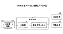
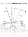
図1には、光走査システムの一例の概略図が示されている。図1に示すように、光走査システム10は、制御装置11の制御に従って光源装置12から照射された光を可動装置13の有する反射面14により偏向して被走査面15を光走査するシステムである。
FIG. 1 shows a schematic diagram of an example of the optical scanning system. As shown in FIG. 1, an
光走査システム10は、制御装置11,光源装置12、反射面14を有する可動装置13により構成される。
The
制御装置11は、例えばCPU(Central Processing Unit)およびFPGA(Field-Programmable Gate Array)等を備えた電子回路ユニットである。可動装置13は、例えば反射面14を有し、反射面14を可動可能なMEMS(Micro Electromechanical Systems)デバイスである。光源装置12は、例えばレーザを照射するレーザ装置である。なお、被走査面15は、例えばスクリーンである。
The
制御装置11は、取得した光走査情報に基づいて光源装置12および可動装置13の制御命令を生成し、制御命令に基づいて光源装置12および可動装置13に駆動信号を出力する。
The
光源装置12は、入力された駆動信号に基づいて光源の照射を行う。可動装置13は、入力された駆動信号に基づいて反射面14を1軸方向または2軸方向の少なくともいずれかに可動させる。
The
これにより、例えば、光走査情報の一例である画像情報に基づいた制御装置11の制御によって、可動装置13の反射面14を所定の範囲で2軸方向に往復可動させ、反射面14に入射する光源装置12からの照射光をある1軸周りに偏向して光走査することにより、被走査面15に任意の画像を投影することができる。
なお、本実施形態の可動装置の詳細および制御装置による制御の詳細については後述する。
Thereby, for example, under the control of the
The details of the movable device and the control by the control device of the present embodiment will be described later.
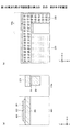
次に、光走査システム10一例のハードウェア構成について図2を用いて説明する。図2は、光走査システム10の一例のハードウェア構成図である。図2に示すように、光走査システム10は、制御装置11、光源装置12および可動装置13を備え、それぞれが電気的に接続されている。このうち、制御装置11は、CPU20、RAM21(Random Access Memory)、ROM22(Read Only Memory)、FPGA23、外部I/F24、光源装置ドライバ25、可動装置ドライバ26を備えている。
Next, a hardware configuration of an example of the
CPU20は、ROM22等の記憶装置からプログラムやデータをRAM21上に読み出し、処理を実行して、制御装置11の全体の制御や機能を実現する演算装置である。
The
RAM21は、プログラムやデータを一時保持する揮発性の記憶装置である。
The
ROM22は、電源を切ってもプログラムやデータを保持することができる不揮発性の記憶装置であり、CPU20が光走査システム10の各機能を制御するために実行する処理用プログラムやデータを記憶している。
The
FPGA23は、CPU20の処理に従って、光源装置ドライバ25および可動装置ドライバ26に適した制御信号を出力する回路である。
The
外部I/F24は、例えば外部装置やネットワーク等とのインタフェースである。外部装置には、例えば、PC(Personal Computer)等の上位装置、USBメモリ、SDカード、CD、DVD、HDD、SSD等の記憶装置が含まれる。また、ネットワークは、例えば自動車のCAN(Controller Area Network)やLAN(Local Area Network)、インターネット等である。外部I/F24は、外部装置との接続または通信を可能にする構成であればよく、外部装置ごとに外部I/F24が用意されてもよい。
The external I /
光源装置トライバは、入力された制御信号に従って光源装置12に駆動電圧等の駆動信号を出力する電気回路である。
The light source device driver is an electric circuit that outputs a drive signal such as a drive voltage to the
可動装置ドライバ26は、入力された制御信号に従って可動装置13に駆動電圧等の駆動信号を出力する電気回路である。
The
制御装置11において、CPU20は、外部I/F24を介して外部装置やネットワークから光走査情報を取得する。なお、CPU20が光走査情報を取得することができる構成であればよく、制御装置11内のROM22やFPGA23に光走査情報を格納する構成としてもよいし、制御装置11内に新たにSSD等の記憶装置を設けて、その記憶装置に光走査情報を格納する構成としてもよい。
In the
ここで、光走査情報とは、被走査面15にどのように光走査させるかを示した情報であり、例えば、光走査により画像を表示する場合は、光走査情報は画像データである。また、例えば、光走査により光書込みを行う場合は、光走査情報は書込み順や書込み箇所を示した書込みデータである。他にも、例えば、光走査により物体認識を行う場合は、光走査情報は物体認識用の光を照射するタイミングと照射範囲を示す照射データである。 Here, the optical scanning information is information indicating how the surface to be scanned 15 is optically scanned. For example, when an image is displayed by optical scanning, the optical scanning information is image data. Further, for example, when optical writing is performed by optical scanning, the optical scanning information is write data indicating a writing order and a writing location. In addition, for example, when object recognition is performed by optical scanning, the optical scanning information is irradiation data indicating the irradiation timing and irradiation range of the object recognition light.
制御装置11は、CPU20の命令および図2に示したハードウェア構成によって、次に説明する機能構成を実現することができる。
The
次に、光走査システム10の制御装置11の機能構成について図3を用いて説明する。図3は、光走査システムの制御装置の一例の機能ブロック図である。
Next, a functional configuration of the
図3に示すように、制御装置11は、機能として制御部30と駆動信号出力部31とを有する。
As shown in FIG. 3, the
制御部30は、例えばCPU20、FPGA23等により実現され、外部装置から光走査情報を取得し、光走査情報を制御信号に変換して駆動信号出力部31に出力する。例えば、制御部30は、外部装置等から画像データを光走査情報として取得し、所定の処理により画像データから制御信号を生成して駆動信号出力部31に出力する。
The
駆動信号出力部31は、光源装置ドライバ25、可動装置ドライバ26等により実現され、入力された制御信号に基づいて光源装置12または可動装置13に駆動信号を出力する。
The drive
駆動信号は、光源装置12または可動装置13の駆動を制御するための信号である。例えば、光源装置12においては、光源の照射タイミングおよび照射強度を制御する駆動電圧である。また、例えば、可動装置13においては、可動装置13の有する反射面14を可動させるタイミングおよび可動範囲を制御する駆動電圧である。
The drive signal is a signal for controlling the drive of the
次に、光走査システム10が被走査面15を光走査する処理について図4を用いて説明する。図4は、光走査システムに係る処理の一例のフローチャートである。
Next, a process in which the
ステップS11において、制御部30は、外部装置等から光走査情報を取得する。
In step S11, the
ステップS12において、制御部30は、取得した光走査情報から制御信号を生成し、制御信号を駆動信号出力部31に出力する。
In step S12, the
ステップS13において、駆動信号出力部31は、入力された制御信号に基づいて駆動信号を光源装置12および可動装置13に出力する。
In step S13, the drive
ステップ14において、光源装置12は、入力された駆動信号に基づいて光照射を行う。また、可動装置13は、入力された駆動信号に基づいて反射面14の可動を行う。光源装置12および可動装置13の駆動により、任意の方向に光が偏向され、光走査される。
In
なお、上記光走査システム10では、1つの制御装置11が光源装置12および可動装置13を制御する装置および機能を有しているが、光源装置用の制御装置および可動装置用の制御装置と、別体に設けてもよい。
In the
また、上記光走査システム10では、一つの制御装置11に光源装置12および可動装置13の制御部30の機能および駆動信号出力部31の機能を設けているが、これらの機能は別体として存在していてもよく、例えば制御部30を有した制御装置11とは別に駆動信号出力部31を有した駆動信号出力装置を設ける構成としてもよい。なお、上記光走査システム10のうち、反射面14を有した可動装置13と制御装置11により、光偏向を行う光偏向システムを構成してもよい。
Further, in the
[画像投影装置]
次に、本実施形態の可動装置を適用した画像投影装置について、図5および図6を用いて詳細に説明する。
[Image projection device]
Next, an image projection device to which the movable device of the present embodiment is applied will be described in detail with reference to FIGS.
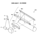
図5は、画像投影装置の一例であるヘッドアップディスプレイ装置500を搭載した自動車400の実施形態に係る概略図である。また、図6はヘッドアップディスプレイ装置500の一例の概略図である。
FIG. 5 is a schematic diagram according to an embodiment of an
画像投影装置は、光走査により画像を投影する装置であり、例えばヘッドアップディスプレイ装置である。 The image projection device is a device that projects an image by optical scanning, and is, for example, a head-up display device.
図5に示すように、ヘッドアップディスプレイ装置500は、例えば、自動車400のウインドシールド(フロントガラス401等)の付近に設置される。ヘッドアップディスプレイ装置500から発せられる投射光Lがフロントガラス401で反射され、ユーザーである観察者(運転者402)に向かう。これにより、運転者402は、ヘッドアップディスプレイ装置500によって投影された画像等を虚像として視認することができる。なお、ウインドシールドの内壁面にコンバイナを設置し、コンバイナによって反射する投射光によってユーザーに虚像を視認させる構成にしてもよい。
As shown in FIG. 5, the head-up
図6に示すように、ヘッドアップディスプレイ装置500は、赤色、緑色、青色のレーザ光源501R,501G,501Bからレーザ光が出射される。出射されたレーザ光は、各レーザ光源に対して設けられるコリメータレンズ502,503,504と、2つのダイクロイックミラー505,506と、光量調整部507と、から構成される入射光学系を経た後、反射面14を有する可動装置13にて偏向される。そして、偏向されたレーザ光は、自由曲面ミラー509と、中間スクリーン510と、投射ミラー511とから構成される投射光学系を経て、スクリーンに投影される。なお、上記ヘッドアップディスプレイ装置500では、レーザ光源501R,501G,501B、コリメータレンズ502,503,504、ダイクロイックミラー505,506は、光源ユニット530として光学ハウジングによってユニット化されている。
As shown in FIG. 6, the head-up
上記ヘッドアップディスプレイ装置500は、中間スクリーン510に表示される中間像を自動車400のフロントガラス401に投射することで、その中間像を運転者402に虚像として視認させる。
The head-up
レーザ光源501R,501G,501Bから発せられる各色レーザ光は、それぞれ、コリメータレンズ502,503,504で略平行光とされ、2つのダイクロイックミラー505,506により合成される。合成されたレーザ光は、光量調整部507で光量が調整された後、反射面14を有する可動装置13によって二次元走査される。可動装置13で二次元走査された投射光Lは、自由曲面ミラー509で反射されて歪みを補正された後、中間スクリーン510に集光され、中間像を表示する。中間スクリーン510は、マイクロレンズが二次元配置されたマイクロレンズアレイで構成されており、中間スクリーン510に入射してくる投射光Lをマイクロレンズ単位で拡大する。
Laser light of each color emitted from the
可動装置13は、反射面14を2軸方向に往復可動させ、反射面14に入射する投射光Lを二次元走査する。この可動装置13の駆動制御は、レーザ光源501R,501G,501Bの発光タイミングに同期して行われる。
The
以上、画像投影装置の一例としてのヘッドアップディスプレイ装置500の説明をしたが、画像投影装置は、反射面14を有した可動装置13により光走査を行うことで画像を投影する装置であればよい。例えば、机等に置かれ、表示スクリーン上に画像を投影するプロジェクタや、観測者の頭部等に装着される装着部材に搭載され、装着部材が有する反射透過スクリーンに投影、または眼球をスクリーンとして画像を投影するヘッドマウントディスプレイ装置等にも、同様に適用することができる。
The head-up
また、画像投影装置は、車両や装着部材だけでなく、例えば、航空機、船舶、移動式ロボット等の移動体、あるいは、その場から移動せずにマニピュレータ等の駆動対象を操作する作業ロボットなどの非移動体に搭載されてもよい。 Further, the image projection device is not only a vehicle or a mounting member, for example, a moving object such as an aircraft, a ship, a mobile robot, or a working robot such as a manipulator that operates a driven object without moving from the place. It may be mounted on a non-moving object.
尚、ヘッドアップディスプレイ装置500は、特許請求の範囲に記載の「ヘッドアップディスプレイ」の一例である。また自動車400は、特許請求の範囲に記載の「車両」の一例である。
The head-up
[光書込装置]
次に、本実施形態の可動装置13を適用した光書込装置について図7および図8を用いて詳細に説明する。
[Optical writing device]
Next, an optical writing device to which the
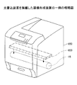
図7は、光書込装置600を組み込んだ画像形成装置の一例である。また、図8は、光書込装置の一例の概略図である。
FIG. 7 is an example of an image forming apparatus incorporating the
図7に示すように、上記光書込装置600は、レーザ光によるプリンタ機能を有するレーザプリンタ650等に代表される画像形成装置の構成部材として使用される。画像形成装置において光書込装置600は、1本または複数本のレーザビームで被走査面15である感光体ドラムを光走査することにより、感光体ドラムに光書込を行う。
As shown in FIG. 7, the
図8に示すように、光書込装置600において、レーザ素子などの光源装置12からのレーザ光は、コリメータレンズなどの結像光学系601を経た後、反射面14を有する可動装置13により1軸方向または2軸方向に偏向される。そして、可動装置13で偏向されたレーザ光は、その後、第一レンズ602aと第二レンズ602b、反射ミラー部602cからなる走査光学系602を経て、被走査面15(例えば感光体ドラムや感光紙)に照射し、光書込みを行う。走査光学系602は、被走査面15にスポット状に光ビームを結像する。また、光源装置12および反射面14を有する可動装置13は、制御装置11の制御に基づき駆動する。
As shown in FIG. 8, in the
このように上記光書込装置600は、レーザ光によるプリンタ機能を有する画像形成装置の構成部材として使用することができる。また、走査光学系を異ならせて1軸方向だけでなく2軸方向に光走査可能にすることで、レーザ光をサーマルメディアに偏向して光走査し、加熱することで印字するレーザラベル装置等の画像形成装置の構成部材として使用することができる。
Thus, the
上記光書込装置に適用される反射面14を有した可動装置13は、ポリゴンミラー等を用いた回転多面鏡に比べ駆動のための消費電力が小さいため、光書込装置の省電力化に有利である。また、可動装置13の振動時における風切り音は回転多面鏡に比べ小さいため、光書込装置の静粛性の改善に有利である。光書込装置は回転多面鏡に比べ設置スペースが圧倒的に少なくて済み、また可動装置13の発熱量もわずかであるため、小型化が容易であり、よって画像形成装置の小型化に有利である。
The
[物体認識装置]
次に、上記本実施形態の可動装置を適用した物体認識装置について、図9および図10を用いて詳細に説明する。
[Object recognition device]
Next, an object recognition device to which the movable device of the present embodiment is applied will be described in detail with reference to FIGS.
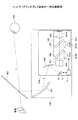
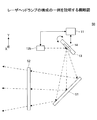
図9は、物体認識装置の一例であるライダ(LiDAR;Laser Imaging Detection and Ranging)装置を搭載した自動車の概略図である。また、図10はライダ装置の一例の概略図である。 FIG. 9 is a schematic diagram of a vehicle equipped with a lidar (LiDAR; Laser Imaging Detection and Ranging) device as an example of an object recognition device. FIG. 10 is a schematic view of an example of the lidar device.
物体認識装置は、対象方向の物体を認識する装置であり、例えばライダ装置である。 The object recognition device is a device that recognizes an object in a target direction, and is, for example, a lidar device.
図9に示すように、ライダ装置700は、例えば自動車701に搭載され、対象方向を光走査して、対象方向に存在する被対象物702からの反射光を受光することで、被対象物702を認識する。
As shown in FIG. 9, the
図10に示すように、光源装置12から出射されたレーザ光は、発散光を略平行光とする光学系であるコリメートレンズ703と、平面ミラー704とから構成される入射光学系を経て、反射面14を有する可動装置13で1軸もしくは2軸方向に走査される。そして、投光光学系である投光レンズ705等を経て装置前方の被対象物702に照射される。光源装置12および可動装置13は、制御装置11により駆動を制御される。被対象物702で反射された反射光は、光検出器709により光検出される。すなわち、反射光は入射光検出受光光学系である集光レンズ706等を経て撮像素子707により受光され、撮像素子707は検出信号を信号処理回路708に出力する。信号処理回路708は、入力された検出信号に2値化やノイズ処理等の所定の処理を行い、結果を測距回路710に出力する。
As shown in FIG. 10, the laser light emitted from the
測距回路710は、光源装置12がレーザ光を発光したタイミングと、光検出器709でレーザ光を受光したタイミングとの時間差、または受光した撮像素子707の画素ごとの位相差によって、被対象物702の有無を認識し、さらに被対象物702との距離情報を算出する。
The
反射面14を有する可動装置13は多面鏡に比べて破損しづらく、小型であるため、耐久性の高い小型のレーダ装置を提供することができる。このようなライダ装置は、例えば車両、航空機、船舶、ロボット等に取り付けられ、所定範囲を光走査して障害物の有無や障害物までの距離を認識することができる。
Since the
上記物体認識装置では、一例としてのライダ装置700の説明をしたが、物体認識装置は、反射面14を有した可動装置13を制御装置11で制御することにより光走査を行い、光検出器により反射光を受光することで被対象物702を認識する装置であればよく、上述した実施形態に限定されるものではない。
In the above-described object recognition device, the
例えば、手や顔を光走査して得た距離情報から形状等の物体情報を算出し、記録と参照することで対象物を認識する生体認証や、対象範囲への光走査により侵入物を認識するセキュリティセンサ、光走査により得た距離情報から形状等の物体情報を算出して認識し、3次元データとして出力する3次元スキャナの構成部材などにも同様に適用することができる。 For example, object information such as shape is calculated from distance information obtained by optical scanning of hands and faces, and biometric authentication that recognizes the target object by recording and referring to it, and recognition of invading objects by optical scanning of the target area The present invention can be similarly applied to a security sensor to be used, a component of a three-dimensional scanner that calculates and recognizes object information such as a shape from distance information obtained by optical scanning, and outputs it as three-dimensional data.
[レーザヘッドランプ]
次に、上記本実施形態の可動装置を自動車のヘッドライトに適用したレーザヘッドランプ50について、図11 を用いて説明する。図11は、レーザヘッドランプ50の構成の一例を説明する概略図である。
[Laser headlamp]
Next, a
レーザヘッドランプ50は、制御装置11と、光源装置12bと、反射面14を有する可動装置13と、ミラー51と、透明板52とを有する。
The
光源装置12bは、青色のレーザ光を発する光源である。光源装置12bから発せられた光は、可動装置13に入射し、反射面14にて反射される。可動装置13は、制御装置11からの信号に基づき、反射面をXY方向に可動し、光源装置12bからの青色のレーザ光をXY方向に二次元走査する。
The
可動装置13による走査光は、ミラー51で反射され、透明板52に入射する。透明板52は、表面又は裏面を黄色の蛍光体により被覆されている。ミラー51からの青色のレーザ光は、透明板52における黄色の蛍光体の被覆を通過する際に、ヘッドライトの色として法定される範囲の白色に変化する。これにより自動車の前方は、透明板52からの白色光で照明される。
The scanning light from the
可動装置13による走査光は、透明板52の蛍光体を通過する際に所定の散乱をする。これにより自動車前方の照明対象における眩しさは緩和される。
The scanning light from the
可動装置13を自動車のヘッドライトに適用する場合、光源装置12b及び蛍光体の色は、それぞれ青及び黄色に限定されない。例えば、光源装置12bを近紫外線とし、透明板52を、光の三原色の青色、緑色及び赤色の各蛍光体を均一に混ぜたもので被覆してもよい。この場合でも、透明板52を通過する光を白色に変換でき、自動車の前方を白色光で照明することができる。
When the
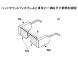
[ヘッドマウントディスプレイ]
次に、上記本実施形態の可動装置を適用したヘッドマウントディスプレイ60について、図12〜13を用いて説明する。ここでヘッドマウントディスプレイ60は、人間の頭部に装着可能な頭部装着型ディスプレイで、例えば、眼鏡に類する形状とすることができる。ヘッドマウントディスプレイを、以降ではHMDと省略して示す。
[Head mounted display]
Next, a head mounted
図12は、HMD60の外観を例示する斜視図である。図12において、HMD60は、左右に1組ずつ略対称に設けられたフロント60a、及びテンプル60bにより構成されている。フロント60aは、例えば、導光板61により構成することができ、光学系や制御装置等は、テンプル60bに内蔵することができる。
FIG. 12 is a perspective view illustrating the appearance of the
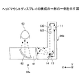
図13は、HMD60の構成を部分的に例示する図である。なお、図13では、左眼用の構成を例示しているが、HMD60は右眼用としても同様の構成を有している。
FIG. 13 is a diagram partially illustrating the configuration of the
HMD60は、制御装置11と、光源ユニット530と、光量調整部507と、反射面14を有する可動装置13と、導光板61と、ハーフミラー62とを有している。
The
光源ユニット530は、上述したように、レーザ光源501R、501G、及び501Bと、コリメータレンズ502、503、及び504と、ダイクロイックミラー505、及び506とを、光学ハウジングによってユニット化したものである。光源ユニット530において、レーザ光源501R、501G、及び501Bからの三色のレーザ光は、ダイクロイックミラー505及び506で合成される。光源ユニット530からは、合成された平行光が発せられる。
As described above, the
光源ユニット530からの光は、光量調整部507により光量調整された後、可動装置13に入射する。可動装置13は、制御装置11からの信号に基づき、反射面14をXY方向に可動し、光源ユニット530からの光を二次元走査する。この可動装置13の駆動制御は、レーザ光源501R、501G、501Bの発光タイミングに同期して行われ、走査光によりカラー画像が形成される。
The light from the
可動装置13による走査光は、導光板61に入射する。導光板61は、走査光を内壁面で反射させながらハーフミラー62に導光する。導光板61は、走査光の波長に対して透過性を有する樹脂等により形成されている。
The scanning light from the
ハーフミラー62は、導光板61からの光をHMD60の背面側に反射し、HMD60の装着者63の眼の方向に出射する。ハーフミラー62は、例えば、自由曲面形状を有している。走査光による画像は、ハーフミラー62での反射により、装着者63の網膜に結像する。或いは、ハーフミラー62での反射と眼球における水晶体のレンズ効果とにより、装着者63の網膜に結像する。またハーフミラー62での反射により、画像は空間歪が補正される。装着者63は、XY方向に走査される光で形成される画像を、観察することができる。
The
62はハーフミラーであるため、装着者63には、外界からの光による像と走査光による画像が重畳して観察される。ハーフミラー62に代えてミラーを設けることで、外界からの光をなくし、走査光による画像のみを観察できる構成としてもよい。
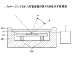
[パッケージング]
次に、本実施形態の可動装置のパッケージングについて図14を用いて説明する。
[Packaging]
Next, the packaging of the movable device according to the present embodiment will be described with reference to FIG.
図14は、パッケージングされた可動装置の第1の例の概略図である。 FIG. 14 is a schematic diagram of a first example of a packaged movable device.
図14に示すように、可動装置13は、パッケージ部材801の内側に配置される取付部材802に取り付けられ、パッケージ部材801の一部を透過部材803で覆われて、密閉されることでパッケージングされる。さらに、パッケージ内は窒素等の不活性ガスが密封されている。これにより、可動装置13の酸化による劣化が抑制され、さらに温度等の環境の変化に対する耐久性が向上する。
As shown in FIG. 14, the
図15は、パッケージングされた可動装置の第2の例を示す図である。 FIG. 15 is a diagram illustrating a second example of a packaged movable device.
図15に示されているように、可動部110を含む可動装置13は、透過部材812を含むパッケージ部材811の内部に、透過部材812に対し傾けるようにして固定される。例えば可動装置13が配置される面と、透過部材812とは非平行である。透過部材812には、パッケージ部材811の内部への光の入射と、パッケージ部材811の内部からの光の出射を規制するパッケージ側開口部813が設けられている。パッケージ側開口部813において、黒い太線で示されている領域は、光を通過させない(遮光する)領域で、黒い太線で挟まれた中央の領域は、光を通過させる領域である。パッケージ側開口部813は、例えば透過部材812において、光を通過させない(遮光する)領域に、光を反射、又は吸収する膜を設けて形成される。
As shown in FIG. 15, the
光源装置12から出射された光はレンズ814で平行化され、光源側開口部815を通過してパッケージ部材811に入射する。光源側開口部815は、光源からの光の強度分布を均一化する等のために、レンズ814で平行化された光の通過を規制する。光源側開口部815においても、パッケージ側開口部813と同様に、黒い太線で示されている領域は、光を通過させない(遮光する)領域で、黒い太線で挟まれた中央の領域は、光を通過させる領域である。光源側開口部815は、例えば所定の開口を有するピンホールである。ピンホールは、例えば、金属板に開口に該当する貫通孔を設けて形成される。
The light emitted from the
パッケージ部材811への入射光は、透過部材812を透過して可動部110に含まれる反射部で反射される。反射光は、透過部材812を透過してパッケージ部材811の内部から外部に向けて出射される。可動部110の駆動により、反射光が像面で走査される。
Light incident on the
点線で示される816及び817は、光源側開口部815による回折光の一部であり、可動装置13においては不要な光である。このような回折光は、パッケージ側開口部813により遮光され、パッケージ部材811には入射しない。また一点鎖線で示される818は、光源側開口部815による回折光の一部が、パッケージ部材811に入射したことによる迷光であり、同様に、可動装置13においては不要な光である。このような迷光は、パッケージ側開口部813により遮光され、パッケージ部材811の内部から出射されないように、可動装置13が配置される面と透過部材812との傾きが設定されている。
図15に示されている構成により、回折光816及び817等の不要な光をパッケージ部材811の内部に入射させないようにし、また迷光818等の不要な光をパッケージ部材811の内部から出射されないようにする。これにより不要な光を像面に到達させないようにすることできる。
With the configuration shown in FIG. 15, unnecessary light such as diffracted
図16は、パッケージングされた可動装置の第3の例を示す図である。 FIG. 16 is a diagram illustrating a third example of a packaged movable device.
図16に示されているように、可動装置13は、透過部材822を含むパッケージ部材821の内部に固定される。図示を省略する光源装置からの光は、透過部材822を透過して可動装置13に入射し、破線で示されている走査光824のように走査される。図中に太線の矢印で示されている有効範囲825は、可動装置13による光の走査の有効範囲である。例えば可動装置13を画像形成装置で用いる場合であれば、有効範囲825は、画像形成領域である。
As shown in FIG. 16, the
図16に示されているように、透過部材822は、パッケージ部材821の内部底面に対して角度θだけ傾斜して固定されている。角度θは、パッケージ部材821の内部から出射される光のうち、透過部材822の外側の面及び内側の面での反射光が有効範囲825に含まれないように設定されている。 角度θは、例えば5°〜65°が好ましく、ここでは15°とされている。これにより、透過部材822での多重反射光のような不要な光を有効範囲825に到達させないようにする。これにより、例えば画像形成装置において画質の低下を防止することができる。
As shown in FIG. 16, the
なお、透過部材822の両面に反射防止膜が形成されている場合でも、製造上、0コンマ数パーセント程度の反射光は発生する。そして反射防止膜での反射光の光量が、可動装置13による走査光の光量に比べて相対的に大きくなる場合がある。図16に示されている構成によれば、このような反射防止膜での反射光等の不要な光も除去することができる。
In addition, even when antireflection films are formed on both surfaces of the
以上に説明した光偏向システム、光走査システム、画像投影装置、光書込装置、物体認識装置、レーザヘッドランプ、及びヘッドマウントディスプレイに使用される本実施形態の可動装置の詳細について、以下で図面を参照しながら説明する。各図面において、同一構成部分には同一符号を付し、重複した説明を省略する場合がある。 The details of the movable device of the present embodiment used for the above-described optical deflection system, optical scanning system, image projection device, optical writing device, object recognition device, laser head lamp, and head mounted display will be described below. This will be described with reference to FIG. In the drawings, the same components are denoted by the same reference numerals, and redundant description may be omitted.
なお、実施形態の説明では、第1軸を回動の中心とした光走査を副走査とし、第2軸を回動の中心とした光走査を主走査とする。また、第1軸及び第2軸を中心とした回動、第1軸及び第2軸を中心とした揺動、並びに第1軸及び第2軸を中心とした可動は、相互に同義である。さらに、矢印により示した方向のうち、X方向は第1軸と平行な方向、Y方向は第2軸と平行な方向、Z方向はXY平面と直交する方向とする。 In the description of the embodiment, optical scanning with the first axis as the center of rotation is referred to as sub-scanning, and optical scanning with the second axis as the center of rotation is referred to as main scanning. The rotation about the first axis and the second axis, the swing about the first axis and the second axis, and the movement about the first axis and the second axis are synonymous with each other. . Further, among the directions indicated by the arrows, the X direction is a direction parallel to the first axis, the Y direction is a direction parallel to the second axis, and the Z direction is a direction orthogonal to the XY plane.
[第1の実施形態]
図17は、第1の実施形態の可動装置の構成の一例を示す平面図である。可動装置13は、第1軸、及び第2軸回りに回動可能な両持ちタイプの可動装置である。
[First Embodiment]
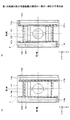
FIG. 17 is a plan view illustrating an example of the configuration of the movable device according to the first embodiment. The
図17に示されているように、可動装置13は、可動部110と、第1駆動部120a及び120bと、第1支持部130と、電極端子140とを有する。また可動部110は、反射面14を含む反射部112と、第2支持部113と、接続部114a及び114bと、トーションバー115a及び115bと、第2駆動部116a及び116bと、調整部117a及び117bとを有する。
As shown in FIG. 17, the
反射部112は、例えばシリコン活性層により形成される。但しこれに限定はされず、酸化材料や無機材料、有機材料等で形成してもよい。反射面14は、反射部112の正のZ方向の面上に形成される。反射面14は、例えば、アルミニウム、金、銀等を含む金属薄膜やその多層膜で、図示されているように、円形状に形成される。
The
反射部112の負のZ方向の面に、反射部112を補強するためのリブを設けてもよい。この場合、リブは、例えばシリコン支持層および酸化シリコン層で形成される。リブを設けることで、可動時に生じる反射部112、及び反射面14の変形歪を抑制することができる。
A rib for reinforcing the reflecting
トーションバー115a及び115bは、Y方向に延在し、Y方向において反射部112を挟み込むように形成される。トーションバー115aの一端は反射部112に接続し、トーションバー115bの一端は反射部112に接続する。反射部112は、トーションバー115a及び115bにより支持される。
The
トーションバー115aの他端は、第2駆動部116aに接続し、トーションバー115bの他端は、第2駆動部116bに接続する。第2駆動部116a及び116bには、弾性梁部の正のZ方向の面に圧電部が設けられる。第2駆動部116aは、電極端子140からレイアウトされる電気配線を通して駆動電圧が印加されると、屈曲変形してトーションバー115aにねじれを生じさせる。同様に、第2駆動部116bは、電極端子140からレイアウトされる電気配線を通して駆動電圧が印加されると、屈曲変形してトーションバー115bにねじれを生じさせる。このようなトーションバー115a及び115bのねじれが回動力となり、反射部112は、第2軸回りに回動する。
The other end of the
第2支持部113は、反射部112と、トーションバー115a及び115bと、第2駆動部116a及び116bとを囲むように形成される。第2支持部113は、第2駆動部116a及び116bに接続し、第2駆動部116a及び116bを支持拘束する。また第2支持部113は、第2駆動部116a及び116bを介して、間接的に反射部112と、トーションバー115a及び115bとを支持する。
The
第2支持部113の図中の右上角には接続部114aが形成され、第2支持部113は、接続部114aを介して第1駆動部120aに接続する。接続部114aは第1駆動部120aとの接続箇所から負のX方向に延在し、第2支持部113の方向に折り返して負のY方向に延在して第2支持部113に接続する。
A
また第2支持部113の図中の左下角には接続部114bが形成され、第2支持部113は、接続部114bを介して第1駆動部120bに接続する。接続部114bは第1駆動部120bとの接続箇所から正のX方向に延在し、第2支持部113の方向に折り返して正のY方向に延在して第2支持部113に接続する。
A connecting
第1駆動部120aと第1駆動部120bは、Y方向において挟み込むように第2支持部113を支持する。
The
第2支持部113の図中の左上角には調整部117aが形成され、また図中の右下角には調整部117bが形成される。調整部117aと調整部117bは、反射部112を挟んで対称な位置に形成される。また調整部117aと調整部117bは、第2支持部113の接続部114a及び114bが形成されていない角部に形成される。なお、調整部117a及び117bの詳細については、別途説明する。
An adjusting
第1駆動部120aは、3つの折り返し部と3つの連結部とを有し、複数の弾性梁部が連結されたミアンダ構造を含む。複数の弾性梁部の正のZ方向の面には、それぞれ圧電部が設けられる。第1駆動部120aの接続部114aと接続していない側の端部は、第1支持部130に接続する。第1支持部130は、第1駆動部120aを支持拘束する。
The
同様に第1駆動部120bは、3つの折り返し部と3つの連結部とを有し、複数の弾性梁部が連結されたミアンダ構造を含む。複数の弾性梁部の正のZ側の面には、それぞれ圧電部が設けられる。第1駆動部120bの接続部114bと接続していない側の端部は、第1支持部130に接続する。第1支持部130は、第1駆動部120bを支持拘束する。
Similarly, the
第1駆動部120a及び120bに設けられた圧電部には、電極端子140からレイアウトされる電気配線を通して駆動電圧が印加される。
A driving voltage is applied to the piezoelectric units provided in the
ここで、第1駆動部120aが有する複数の弾性梁部うち、最も反射部112に距離が近いものから数えて奇数番目の弾性梁部に設けられた圧電部を圧電駆動部群150Aとする。また第1駆動部120bが有する複数の弾性梁部のうち、最も反射部112に距離が近いものから数えて偶数番目の弾性梁部に設けられた圧電部を同様に圧電駆動部群150Aとする。圧電駆動部群150Aは、駆動電圧が各圧電部に対して同時に印加されると、同一方向に屈曲変形する。この変形を回動力として、可動部110が第1軸回りに回動する。
Here, among the plurality of elastic beams included in the
一方、第1駆動部120aが有する弾性梁部のうち、最も反射部112に距離が近いものから数えて偶数番目の弾性梁部に設けられた圧電部を圧電駆動部群150Bとする。また第1駆動部120bが有する弾性梁部のうち、最も反射部112に距離が近いものから数えて奇数番目の弾性梁部を同様に圧電駆動部群150Bとする。圧電駆動部群150Bは、駆動電圧が各圧電部に対して同時に印加されると、同一方向に屈曲変形する。この変形を回動力として、可動部110が、圧電駆動部群150Aによる回動とは逆方向に第1軸回りに回動する。
On the other hand, among the elastic beams included in the
第1駆動部120a及び120bでは、圧電駆動部群150A及び150Bが有する複数の圧電部を同時に屈曲変形させることで、屈曲変形による回動量を累積させ、可動部110の第1軸回りの振れ角度を大きくすることができる。電圧印加による圧電駆動部群150Aによる可動部110の回動量と、電圧印加による圧電駆動部群150Bによる可動部110の回動量が釣り合っている時は、振れ角はゼロとなる。
In the
次に、図17において一点鎖線で示されている領域Pの詳細を、図18を用いて説明する。図18(a)は、図17に二点鎖線で示されている断面のQ−Q矢視断面図である。 Next, details of the region P indicated by a dashed line in FIG. 17 will be described with reference to FIG. FIG. 18A is a cross-sectional view taken along line QQ of a cross-section indicated by a two-dot chain line in FIG. 17.
図18(a)において、第1駆動部120bに含まれる弾性梁部300は、シリコン活性層200と、下部電極301と、圧電部302と、上部電極303とを有する。シリコン活性層200の正のZ方向の面に、正のZ方向に向けて下部電極301、圧電部302、及び上部電極303が順に形成される。
In FIG. 18A, the
上部電極303、及び下部電極301は、例えば金(Au)や白金(Pt)等の材料を用いて形成される。また上部電極303と下部電極301の少なくとも一方の電極の先端角は、鈍角状になっている。
The
圧電部302は、例えば圧電性を有するPZT(チタン酸ジルコン酸鉛)等の材料を用いて形成される。第1駆動部120a及び120bに含まれる複数の弾性梁部は、何れも図18(a)に示されている弾性梁部300と同様の層構成を有する。また第2駆動部116a及び116bも同様の層構成を有する。
The
特に、第2駆動部116a(図17参照)では、上部電極と下部電極の少なくとも一方は、トーションバー115aに接続する部分の角部が円弧形状、又はテーパ形状に形成されている。より好ましくは、上部電極と下部電極の両方が同じく円弧形状、又はテーパ形状に形成されている。同様に第2駆動部116b(図17参照)では、上部電極と下部電極の少なくとも一方は、トーションバー115bに接続する部分の角部が円弧形状、又はテーパ形状に形成されている。より好ましくは、上部電極と下部電極の両方が同じく円弧形状、又はテーパ形状に形成されている。
In particular, in the
なお、本実施形態では、第2駆動部116a及び116bを、それぞれの両端が第2支持部113に接続する両持ち梁構造とする例を示したが、第2駆動部116a及び116bを片持ち梁構造としてもよい。片持ち梁構造においては、第2駆動部116aの一端は第2支持部113に接続し、他端はトーションバー115aに接続する。また第2駆動部116bの一端は第2支持部113に接続し、他端はトーションバー115bに接続する。
In the present embodiment, an example has been described in which the
片持ち梁構造とした場合には、第2駆動部116a及び116bに設けられた上部電極と下部電極の少なくとも一方は、トーションバーに接続している側の先端の角部が円弧形状またはテーパ形状に形成される。より好ましくは、上部電極と下部電極の両方が同じく円弧形状またはテーパ形状に形成される。
In the case of the cantilever structure, at least one of the upper electrode and the lower electrode provided in the
図18(a)において、圧電部302は、電極端子140からレイアウトされる電気配線を介して外部の制御装置に電気的に接続し、駆動電圧を印加されて駆動する。また、第1駆動部120a及び120bを二酸化ケイ素(SiO2)のような絶縁層で覆い、絶縁層の正のZ方向の面に電気配線を形成してもよい。
In FIG. 18A, the
接続部114bは、シリコン活性層200と、層間膜201と、シリコン支持層202とを有する。シリコン活性層200の負のZ方向の面に、負のZ方向に向けて層間膜201、及びシリコン支持層202が順に形成される。層間膜201は、例えば一酸化ケイ素(SiO)等の材料を用いて形成され、シリコン支持層202は、例えば単結晶シリコン等から形成される。接続部114bの正のZ方向の面に絶縁膜や電気配線を形成してもよい。
The
図18(b)は、図17に一点鎖線で示されている領域Pの背面図である。シリコン活性層200の負のZ方向の面にシリコン支持層202が図示されるように形成され、配置される。接続部114bでは、シリコン支持層202が第1駆動部120bの弾性梁部300に届くように形成されてもよい。
FIG. 18B is a rear view of a region P indicated by a chain line in FIG. A
次に、調整部117a及び117bについて説明する。上述のように、調整部117a及び117bは、第2支持部113において、接続部114a及び114bが形成されていない角部に形成され、反射部112を挟んで対称な位置に配置される。調整部117a及び117bは、図18(a)に示されている接続部114bと同様の層構成を有する。
Next, the
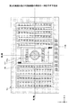
ここで、図17において、破線で示されている領域Rの背面図を図19に示す。尚、図19の背面図では、分かりやすさの便宜のため、例えば図17における接続部114aが、図19においても同じ位置に配置されるように示している。
Here, FIG. 19 shows a rear view of a region R indicated by a broken line in FIG. In the rear view of FIG. 19, for the sake of simplicity, for example, the
図19は、第2支持部113に含まれるシリコン活性層200の負のZ方向の面にシリコン支持層202が形成され、配置された例を示している。図19(a)は、シリコン支持層202の配置の第1の例を示す図である。
FIG. 19 shows an example in which the
図19(a)では、シリコン支持層202は、第2支持部113の背面側に設けられている。またシリコン支持層202は、接続部114a及び114bにおけるY方向に延在する箇所の背面側に設けられ、また調整部117a及び117bの背面側に設けられている。第2支持部113に調整部117a及び117bを形成することで、第2軸を挟んで線対称にシリコン支持層202を設けることができる。これにより、反射部112を挟んだ可動部110の重量の対称性を確保することができる。
In FIG. 19A, the
例えば、第1駆動部120a及び120bが、それぞれ可動部110の一部でのみ接続すると、接続する箇所の重量等に起因して、反射部112を中心とした重量の対称性が崩れる場合がある。重量の対称性が崩れると、可動部110の重心位置がずれ、可動部110の第1軸、及び第2軸回りの回動が不安定になる。図19(a)に示されるように、調整部117a及び117bを設けて重量の対称性を確保することで、可動部110の重心位置のずれを防止し、可動部110の回動の安定性を確保することができる。
For example, if the
図19(b)は、シリコン支持層202の配置の第2の例を示す図である。図19(b)では、シリコン支持層202は、第2支持部113の背面側に設けられている。またシリコン支持層202は、接続部114a及び114bにおけるX方向及びY方向に延在する箇所の背面側に設けられ、また調整部117a及び117bの背面側に設けられている。接続部114a及び114bにおいて、X方向に延在する箇所にもシリコン支持層202が設けられているため、その分だけ重量が増している。そのため、調整部117a及び117bに設けられたシリコン支持層202の幅(X方向の長さ)を、接続部114a及び114bに設けられたシリコン支持層202の幅より太くすることで、反射部112を挟んだ可動部110の重量の対称性を確保している。
FIG. 19B is a diagram illustrating a second example of the arrangement of the
このように、調整部117a及び117bの幅、長さ、及び厚みや、調整部117a及び117bに設けるシリコン支持層202の幅、長さ、及び厚みを調整することで、反射部112を挟んだ可動部110の重量の対称性を確保できる。そして可動部110の第1軸、及び第2軸回りの回動の安定性を確保することができる。調整部117a及び117bの幅、長さ、及び厚みや、調整部117a及び117bに設けるシリコン支持層202の幅、長さ、及び厚みは、予め実験やシミュレーションで、重量の対称性を確保するための適正値が求められる。
As described above, by adjusting the width, length, and thickness of the
幅、長さ、及び厚みといった寸法だけでなく、調整部117a及び117bや、調整部117a及び117bに設ける層の材質を変えて重量を調整してもよい。また厚みを変化させる場合は、厚みを部分的に大きくするようにしてもよい。 例えば、反射部112に近付くにつれ、調整部117a及び117bや、調整部117a及び117bに設ける層の厚みを徐々に厚く、又は薄くしてもよい。このようにすることで、可動装置13の形状や構成に対応させながら、柔軟な調整方法により、可動部110の重量の対称性を確保することができる。
The weight may be adjusted by changing not only the dimensions such as the width, the length, and the thickness but also the materials of the adjusting
上記の可動装置13の基板には、例えばSOI(Silicon On Insulator)基板等の半導体を用いることができる。半導体プロセスにより加工することで、調整部117a及び117bを含めた各構成要素を一体的に形成することができる。なお、第1駆動部120a及び120b、並びに第2駆動部116a及び116bの形成は、SOI基板を成形した後に行ってもよいし、SOI基板の成形中に行ってもよい。
As the substrate of the
調整部117a及び117bの幅や長さといった寸法は、可動装置13を製造後に、ポストプロセスで変化させることも可能である。これにより、可動部110の重心位置等をポストプロセスで調整することができ、可動部110の回動の安定性の柔軟な調整が可能となる。
The dimensions such as the width and length of the
上記では、圧電部をシリコン活性層200の正のZ方向の面に形成する例を説明したが、シリコン活性層200の負のZ方向の面に設けてもよいし、シリコン活性層200の両面に設けてもよい。
In the above, the example in which the piezoelectric portion is formed on the surface of the silicon
反射部112を第1軸回り、又は第2軸回りに回動させられるのであれば、各構成要素の形状は本実施形態で説明した形状に限定されない。例えば、トーションバー115a及び115b、第1駆動部120a及び120b、第2駆動部116a及び116b等は、平面形状でなく曲率を有する形状にしても構わない。
The shape of each component is not limited to the shape described in the present embodiment, as long as the reflecting
次に、可動装置13の駆動方法の一例を、図17を参照して説明する。第2軸回りの回動のために、反射部112と、トーションバー115a及び115bと、第2駆動部116a及び116bの一体構造の共振周波数で、第2駆動部116a及び116bに駆動電圧が印加される。共振周波数は、例えば20kHzである。
Next, an example of a method of driving the
トーションバー115aの一端が接続した第2駆動部116aの圧電部302は、上部電極303、及び下部電極301を通じて駆動電圧が印加されると変形する。圧電部302の変形により、第2駆動部116aは屈曲変形し、トーションバー115aがねじれる。
The
同様に、トーションバー115bの一端が接続した第2駆動部116bの圧電部302は、上部電極303、及び下部電極301を通じて駆動電圧が印加されると変形する。圧電部302の変形により、第2駆動部116bは屈曲変形し、トーションバー115bがねじれる。
Similarly, the
トーションバー115a及び115bのねじれが回動力となり、反射部112は第2軸回りに往復回動する。第2駆動部116a及び116bに印加される駆動電圧の波形は、例えば正弦波である。反射部112は、正弦波の駆動電圧波形の周期で共振駆動し、往復回動する。
The torsion of the
第1軸回りの回動においては、圧電駆動部群150Aに印加される駆動電圧の波形は、例えばノコギリ波状の波形を含む。また駆動電圧の周波数は、例えば60HZである。駆動電圧の波形は、電圧値が極小値から次の極大値まで増加する立ち上がり期間の時間幅をTr、電圧値が極大値から次の極小値まで減少する立ち下がり期間の時間幅をTfとすると、例えば、Tr:Tf=9:1となる比率があらかじめ設定されている。このとき、一周期に対するTrの比率を駆動電圧のシンメトリという。
In the rotation around the first axis, the waveform of the drive voltage applied to the piezoelectric
圧電駆動部群150Bに印加される駆動電圧の波形は、同様に、例えばノコギリ波状の波形を含む。また駆動電圧の周波数は、例えば60HZである。駆動電圧の波形は、例えば、Tf:Tr=9:1となる比率があらかじめ設定されている。
Similarly, the waveform of the drive voltage applied to the piezoelectric
圧電駆動部群150Aに印加される駆動電圧の波形の周期と、圧電駆動部群150Bに印加される駆動電圧の波形の周期は、同一となるように設定されている。
The cycle of the waveform of the drive voltage applied to the piezoelectric
上記の駆動電圧のノコギリ波状の波形は、正弦波の重ね合わせによって生成される。また、本実施形態では、駆動電圧の波形としてノコギリ波状の波形を用いる例を示したが、これに限定はされない。例えばノコギリ波状の波形の頂点を丸くした波形の駆動電圧や、ノコギリ波状の波形の直線領域を曲線とした波形の駆動電圧など、可動装置のデバイス特性に応じて波形を変えることも可能である。 The sawtooth waveform of the drive voltage is generated by superimposing sine waves. Further, in the present embodiment, an example is shown in which a sawtooth waveform is used as the waveform of the drive voltage, but the present invention is not limited to this. For example, the waveform can be changed according to the device characteristics of the movable device, such as a driving voltage having a waveform in which the peak of the sawtooth waveform is rounded, or a driving voltage having a waveform in which the linear region of the sawtooth waveform is curved.
駆動電圧を印加された場合の第1駆動部120a及び120bの動作は上述の通りで、圧電駆動部群150A及び150Bの屈曲変形により、可動部110が第1軸回りに往復回動する。
The operation of the
なお、第1軸回りの回動、及び第2軸回りの回動は、特許請求の範囲に記載の「駆動」の一例である。 The rotation about the first axis and the rotation about the second axis are examples of “driving” described in the claims.
以上説明してきたように、本実施形態によれば、調整部117a及び117bを設けることで、可動部110の重量の対称性を確保できる。これにより可動部110の重心位置のずれを防止し、可動部110の回動等の駆動を安定化させることができる。
As described above, according to the present embodiment, by providing the
[第2の実施形態]
次に、第2の実施形態の可動装置を、図20を参照して説明する。なお、第2の実施形態において、既に説明した実施形態と同一構成部分についての説明は省略する場合がある。
[Second embodiment]
Next, a movable device according to a second embodiment will be described with reference to FIG. In the second embodiment, the description of the same components as those of the already described embodiment may be omitted.
図20は、第2の実施形態の可動装置13aの構成の一例を示す平面図である。可動装置13aは可動部110aを有し、可動部110aは調整部118a及び118bを有する。調整部118a及び118bは、それぞれシリコン支持層202のみで形成される。シリコン支持層202の幅、長さ、及び厚みを調整することで、反射部112を挟んだ可動部110aの重量の対称性を確保することができる。このような調整部118a及び118bの幅、長さ、及び厚みは、予め実験やシミュレーションで、重量の対称性を確保するための適正値が求められる。
FIG. 20 is a plan view illustrating an example of the configuration of the
なお、上記ではシリコン支持層202のみで調整部118a及び118bを形成する例を示したが、シリコン活性層200のみで形成してもよい。
In the above description, the example in which the
なお、これ以外の効果は、第1の実施形態で説明したものと同様である。 The other effects are the same as those described in the first embodiment.
[第3の実施形態]
次に、第3の実施形態の可動装置を、図21を参照して説明する。なお、第3の実施形態において、既に説明した実施形態と同一構成部分についての説明は省略する場合がある。
[Third Embodiment]
Next, a movable device according to a third embodiment will be described with reference to FIG. In the third embodiment, the description of the same components as those in the above-described embodiment may be omitted.
図21は、1軸の可動装置13bの構成の一例を示す図である。可動装置13bは可動部110bを有し、可動部110bは、反射面14を含む第2支持部160と、調整部119a及び119bとを有する。可動部110bは第1軸回りに回動可能である。
FIG. 21 is a diagram illustrating an example of the configuration of the one-axis
調整部119a及び119bは、それぞれシリコン活性層200のみで形成される。シリコン活性層200の幅、長さ、及び厚みを調整することで、可動部110bの重量の対称性を確保することができる。なお、シリコン活性層200のみで調整部119a及び119bを形成する例を示したが、シリコン活性層200のみで形成してもよい。
The
本実施形態によれば、1軸の可動装置13bにおいても、調整部119a及び119bを設けることで、可動部110bの重量の対称性を確保して重心位置のずれを防止し、可動部110bの回動等の駆動を安定化させることができる。
According to the present embodiment, even in the one-axis
なお、これ以外の効果は、2軸の可動装置に限定される効果を除き、第1の実施形態で説明したものと同様である。 The other effects are the same as those described in the first embodiment, except for the effect limited to the two-axis movable device.
以上、本発明の実施形態の例について記述したが、本発明は斯かる特定の実施形態に限定されるものではなく、特許請求の範囲に記載された本発明の要旨の範囲内において、種々の変形・変更が可能である。 As described above, the example of the embodiment of the present invention has been described. However, the present invention is not limited to such a specific embodiment, and various modifications may be made within the scope of the present invention described in the appended claims. Deformation and modification are possible.
10 光走査システム
11、41 制御装置
12、12b 光源装置
13、13a、13b 可動装置
14 反射面
15 被走査面
25 光源装置ドライバ
26 可動装置ドライバ
30、42 制御部
31、43 駆動信号出力部
44 検出信号取得部
45 弾性率調整用駆動信号出力部
50 レーザヘッドランプ
51 ミラー
52 透明板
60 ヘッドマウントディスプレイ
60a フロント
60b テンプル
61 導光板
62 ハーフミラー
63 装着者
110 可動部
112 反射部
113、160 第2支持部
114a、114b 接続部
115a、115b トーションバー
116a、116b 第2駆動部
117a、117b、118a、118b、119a、119b 調整部
120a、120b 第1駆動部
130 第1支持部
140 電極端子
150A、150B 圧電駆動部群
200 シリコン活性層
201 層間膜
202 シリコン支持層
301 下部電極
302 圧電部
303 上部電極
400 自動車(車両の一例)
500 ヘッドアップディスプレイ装置(画像投影装置の一例、ヘッドアップディスプレイの一例)
650 レーザプリンタ
700 ライダ装置(物体認識装置の一例)
702 被対象物
801、811、821 パッケージ部材
802 取付部材
803、812、822 透過部材
500 Head-up display device (an example of an image projection device, an example of a head-up display)
650
702
Claims (13)
前記可動部に接続し、前記可動部を駆動させる第1駆動部と、
前記第1駆動部に接続し、前記第1駆動部を支持する第1支持部と、を有する可動装置であって、
前記可動部は、前記反射部を挟んで対称に配置された調整部を含む可動装置。 A movable part having a reflection part,
A first drive unit connected to the movable unit and driving the movable unit;
A first support unit connected to the first drive unit and supporting the first drive unit,
The movable device, wherein the movable unit includes an adjusting unit symmetrically arranged with the reflecting unit interposed therebetween.
前記第1駆動部に接続する第2支持部と、
第2支持部に支持され、前記反射部に接続し、前記反射部を駆動させる第2駆動部と、を有する請求項1、又は2に記載の可動装置。 The movable part is
A second support unit connected to the first drive unit;
The movable device according to claim 1, further comprising: a second driving unit supported by a second support unit, connected to the reflection unit, and driving the reflection unit.
前記第2駆動部は、前記反射部を第2軸回りに回動させ、
前記可動部の重心は、前記第1軸、及び前記第2軸の少なくとも1つの上に位置する請求項3乃至5の何れか1項に記載の可動装置。 The first drive section rotates the movable section around a first axis,
The second drive section rotates the reflection section around a second axis,
The movable device according to claim 3, wherein a center of gravity of the movable portion is located on at least one of the first axis and the second axis.
Priority Applications (2)
| Application Number | Priority Date | Filing Date | Title |
|---|---|---|---|
| JP2018120205A JP7167500B2 (en) | 2018-06-25 | 2018-06-25 | Mobile devices, image projection devices, head-up displays, laser headlamps, head-mounted displays, object recognition devices, and vehicles |
| US16/441,641 US10901220B2 (en) | 2018-06-25 | 2019-06-14 | Movable device, image projection apparatus, heads-up display, laser headlamp, head-mounted display, object recognition device, and vehicle |
Applications Claiming Priority (1)
| Application Number | Priority Date | Filing Date | Title |
|---|---|---|---|
| JP2018120205A JP7167500B2 (en) | 2018-06-25 | 2018-06-25 | Mobile devices, image projection devices, head-up displays, laser headlamps, head-mounted displays, object recognition devices, and vehicles |
Publications (2)
| Publication Number | Publication Date |
|---|---|
| JP2020003531A true JP2020003531A (en) | 2020-01-09 |
| JP7167500B2 JP7167500B2 (en) | 2022-11-09 |
Family
ID=68981676
Family Applications (1)
| Application Number | Title | Priority Date | Filing Date |
|---|---|---|---|
| JP2018120205A Active JP7167500B2 (en) | 2018-06-25 | 2018-06-25 | Mobile devices, image projection devices, head-up displays, laser headlamps, head-mounted displays, object recognition devices, and vehicles |
Country Status (2)
| Country | Link |
|---|---|
| US (1) | US10901220B2 (en) |
| JP (1) | JP7167500B2 (en) |
Cited By (1)
| Publication number | Priority date | Publication date | Assignee | Title |
|---|---|---|---|---|
| JP2021189323A (en) * | 2020-06-01 | 2021-12-13 | 株式会社リコー | Movable device, deflection device, distance measuring device, image projection device, and vehicle |
Families Citing this family (7)
| Publication number | Priority date | Publication date | Assignee | Title |
|---|---|---|---|---|
| WO2017064797A1 (en) * | 2015-10-15 | 2017-04-20 | 日立マクセル株式会社 | Information display device |
| JP7363177B2 (en) | 2019-08-07 | 2023-10-18 | 株式会社リコー | Optical deflector, optical scanning system, image projection device, image forming device, laser radar |
| US11750779B2 (en) | 2019-08-20 | 2023-09-05 | Ricoh Company, Ltd. | Light deflector, optical scanning system, image projection device, image forming apparatus, and lidar device |
| JP7481099B2 (en) * | 2019-09-11 | 2024-05-10 | 浜松ホトニクス株式会社 | Manufacturing method for optical scanning system, manufacturing method for optical scanning device, and data acquisition method |
| US11789258B2 (en) | 2019-11-27 | 2023-10-17 | Ricoh Company, Ltd. | Light deflector, deflecting device, object recognition device, image projection device, and mobile object |
| US11796793B2 (en) | 2019-11-27 | 2023-10-24 | Ricoh Company, Ltd. | Optical deflector, deflection apparatus, distance measuring apparatus, image projecting apparatus, and movable body |
| JP7459580B2 (en) * | 2020-03-16 | 2024-04-02 | 株式会社リコー | Mobile devices, image projection devices, head-up displays, laser headlamps, head-mounted displays, object recognition devices, and moving objects |
Citations (7)
| Publication number | Priority date | Publication date | Assignee | Title |
|---|---|---|---|---|
| US20040183149A1 (en) * | 2001-07-26 | 2004-09-23 | Harald Schenk | Micromechanical device |
| JP2011095290A (en) * | 2009-10-27 | 2011-05-12 | Seiko Epson Corp | Optical deflection element, optical deflector and image forming apparatus |
| JP2013020124A (en) * | 2011-07-12 | 2013-01-31 | Ricoh Co Ltd | Optical deflector, optical scanner, image forming device, and image projection device |
| JP2015087443A (en) * | 2013-10-29 | 2015-05-07 | セイコーエプソン株式会社 | Optical scanner, image display device, head-mounted display, and head-up display |
| JP2016009050A (en) * | 2014-06-24 | 2016-01-18 | スタンレー電気株式会社 | Optical deflector |
| JP2016081037A (en) * | 2014-10-15 | 2016-05-16 | 株式会社リコー | Light deflector, two-dimensional image display device, optical scanner, and image forming apparatus |
| JP2017068205A (en) * | 2015-10-02 | 2017-04-06 | ミツミ電機株式会社 | Optical scanning module and optical scanning control device |
Family Cites Families (25)
| Publication number | Priority date | Publication date | Assignee | Title |
|---|---|---|---|---|
| US6177667B1 (en) | 1997-10-03 | 2001-01-23 | Ricoh Company, Ltd. | Imaging device |
| JP4520402B2 (en) | 2005-12-07 | 2010-08-04 | 株式会社リコー | Multi-wavelength light switching element, multi-wavelength light switching device, color light switching element, color light switching device, multi-wavelength light switching element array, color light switching element array, multi-color image display device and color image display device |
| JP5195112B2 (en) | 2008-07-18 | 2013-05-08 | 株式会社リコー | Refractive index sensor, refractive index sensor array and biosensor |
| JP5315845B2 (en) | 2008-08-07 | 2013-10-16 | 株式会社リコー | Illumination device and projection-type image display device |
| JP5493735B2 (en) | 2009-01-30 | 2014-05-14 | 株式会社リコー | Deflection mirror, optical scanning device, image forming device, and image projection device |
| JP5728823B2 (en) | 2009-06-09 | 2015-06-03 | 株式会社リコー | Optical deflector, optical scanning device, image forming apparatus, and image projecting apparatus |
| US8654424B2 (en) | 2009-09-15 | 2014-02-18 | Ricoh Company, Ltd. | Multibeam deflector for separating beams output from optical deflection devices |
| JP5742141B2 (en) | 2009-09-18 | 2015-07-01 | 株式会社リコー | Optical scanning device |
| US9927611B2 (en) * | 2010-03-29 | 2018-03-27 | Soraa Laser Diode, Inc. | Wearable laser based display method and system |
| JP5842467B2 (en) | 2010-11-16 | 2016-01-13 | 株式会社リコー | Actuator device, protective cover for the actuator device, method for manufacturing the actuator, light deflection device using the actuator device, two-dimensional optical scanning device, and image projection device using the same |
| JP6201528B2 (en) | 2012-11-15 | 2017-09-27 | 株式会社リコー | Optical deflection apparatus, image forming apparatus, head-up display, and vehicle |
| JP6168353B2 (en) * | 2013-09-13 | 2017-07-26 | 株式会社リコー | Optical deflection apparatus, image forming apparatus, vehicle, optical deflection apparatus control method, and optical deflection apparatus adjustment method |
| CN106133329B (en) * | 2014-03-17 | 2020-01-17 | 胡斯华纳有限公司 | Power equipment cooling system |
| US9766450B2 (en) * | 2014-10-15 | 2017-09-19 | Ricoh Company, Ltd. | Light deflector, two-dimensional image display apparatus, optical scanner, and image forming apparatus |
| JP6216307B2 (en) * | 2014-11-17 | 2017-10-18 | 矢崎総業株式会社 | Head-up display device and backlight device |
| JP6459422B2 (en) | 2014-11-17 | 2019-01-30 | 株式会社リコー | Optical deflector, optical scanning device, image forming device, image projection device, head-up display, and laser radar |
| JP6485013B2 (en) | 2014-11-27 | 2019-03-20 | 株式会社リコー | Optical deflector, image display device, and object device |
| JP6439802B2 (en) | 2014-12-08 | 2018-12-19 | 株式会社リコー | Optical deflector, image display device, and object device |
| US20180084232A1 (en) * | 2015-07-13 | 2018-03-22 | Michael Belenkii | Optical See-Through Head Worn Display |
| US9910271B2 (en) * | 2015-12-21 | 2018-03-06 | Ricoh Company, Ltd. | Actuator device, optical deflector, an image projection apparatus, and image forming apparatus |
| WO2017110694A1 (en) | 2015-12-22 | 2017-06-29 | 株式会社リコー | Rotation device, optical scanning device, and image display device |
| US10404954B2 (en) * | 2016-01-21 | 2019-09-03 | Ricoh Company, Ltd. | Optical deflection apparatus, image projector, optical writing unit, and object recognition device |
| EP3220183B1 (en) | 2016-03-17 | 2021-11-10 | Ricoh Company, Ltd. | Control unit, optical deflection system, image projection apparatus, and control method |
| US10663974B2 (en) * | 2016-11-23 | 2020-05-26 | Electronics And Telecommunications Research Institute | Object recognition device, autonomous driving system including the same, and object recognition method using the object recognition device |
| JP6839806B2 (en) * | 2017-09-21 | 2021-03-10 | パナソニックIpマネジメント株式会社 | Head-up display device and vehicle |
-
2018
- 2018-06-25 JP JP2018120205A patent/JP7167500B2/en active Active
-
2019
- 2019-06-14 US US16/441,641 patent/US10901220B2/en active Active
Patent Citations (7)
| Publication number | Priority date | Publication date | Assignee | Title |
|---|---|---|---|---|
| US20040183149A1 (en) * | 2001-07-26 | 2004-09-23 | Harald Schenk | Micromechanical device |
| JP2011095290A (en) * | 2009-10-27 | 2011-05-12 | Seiko Epson Corp | Optical deflection element, optical deflector and image forming apparatus |
| JP2013020124A (en) * | 2011-07-12 | 2013-01-31 | Ricoh Co Ltd | Optical deflector, optical scanner, image forming device, and image projection device |
| JP2015087443A (en) * | 2013-10-29 | 2015-05-07 | セイコーエプソン株式会社 | Optical scanner, image display device, head-mounted display, and head-up display |
| JP2016009050A (en) * | 2014-06-24 | 2016-01-18 | スタンレー電気株式会社 | Optical deflector |
| JP2016081037A (en) * | 2014-10-15 | 2016-05-16 | 株式会社リコー | Light deflector, two-dimensional image display device, optical scanner, and image forming apparatus |
| JP2017068205A (en) * | 2015-10-02 | 2017-04-06 | ミツミ電機株式会社 | Optical scanning module and optical scanning control device |
Cited By (2)
| Publication number | Priority date | Publication date | Assignee | Title |
|---|---|---|---|---|
| JP2021189323A (en) * | 2020-06-01 | 2021-12-13 | 株式会社リコー | Movable device, deflection device, distance measuring device, image projection device, and vehicle |
| JP7456294B2 (en) | 2020-06-01 | 2024-03-27 | 株式会社リコー | Movable devices, deflection devices, distance measuring devices, image projection devices, and vehicles |
Also Published As
| Publication number | Publication date |
|---|---|
| JP7167500B2 (en) | 2022-11-09 |
| US20190391394A1 (en) | 2019-12-26 |
| US10901220B2 (en) | 2021-01-26 |
Similar Documents
| Publication | Publication Date | Title |
|---|---|---|
| JP7167500B2 (en) | Mobile devices, image projection devices, head-up displays, laser headlamps, head-mounted displays, object recognition devices, and vehicles | |
| US20210041687A1 (en) | Light deflector, optical scanning system, image projection device, image forming apparatus, and lidar device | |
| JP7501762B2 (en) | Movable device, image projection device, head-up display, laser headlamp, head-mounted display, object recognition device, and vehicle | |
| EP3805839B1 (en) | Light deflector, deflecting device, distance-measuring apparatus, image projection device, and vehicle | |
| JP2020154053A (en) | Optical deflection element and method for manufacturing the same, optical deflection system, and optical scanning system | |
| JP2020101587A (en) | Movable device, distance measuring device, image projection device, and vehicle | |
| US11624903B2 (en) | Light deflector, LiDAR device, and image forming apparatus | |
| JP2020101588A (en) | Movable device, distance measuring device, image projection device, vehicle, and seating | |
| US11947113B2 (en) | Movable device, image projection apparatus, head-up display, laser headlamp, head-mounted display, object recognition device, and vehicle | |
| US20220299757A1 (en) | Movable device, image projection apparatus, laser headlamp, head-mounted display, distance measurement device, and mobile object | |
| US11640053B2 (en) | Movable device, image projection apparatus, heads-up display, laser headlamp, head-mounted display, object recognition device, and mobile object | |
| JP7338403B2 (en) | Optical deflectors, image projection devices, head-up displays, laser headlamps, head-mounted displays, object recognition devices, and vehicles | |
| JP7363352B2 (en) | Mobile devices, image projection devices, head-up displays, laser headlamps, head-mounted displays, object recognition devices, and vehicles | |
| US12091309B2 (en) | Movable device, distance measurement device, image projection apparatus, vehicle, and mount | |
| JP7247553B2 (en) | Mobile devices, image projection devices, head-up displays, laser headlamps, head-mounted displays, object recognition devices, and vehicles | |
| JP7396147B2 (en) | Movable devices, optical deflection devices, image projection devices, optical writing devices, object recognition devices, moving objects, head-mounted displays | |
| US20220155582A1 (en) | Operating device, light deflector, light deflecting device, distance measurement apparatus, image projection apparatus, and mobile object | |
| US20220299755A1 (en) | Light deflector, image projection apparatus, laser headlamp, head-mounted display, distance measurement apparatus, and mobile object | |
| US20230324677A1 (en) | Movable device, projection apparatus, and head-up display | |
| US20220326512A1 (en) | Movable apparatus | |
| JP6809281B2 (en) | Optical deflector, optical scanning device, image projection device, and object recognition device | |
| JP2023140219A (en) | Movable device, light deflection element, image projection apparatus, head-up display, laser headlamp, head-mounted display, object recognition apparatus and movable body | |
| JP2024068414A (en) | Movable device, optical scanning system, head-up display, laser head lamp, head-mounted display, object recognition device, and moving body | |
| JP2021085983A (en) | Optical deflector, deflecting device, distance measuring device, image projection device, and vehicle |
Legal Events
| Date | Code | Title | Description |
|---|---|---|---|
| A621 | Written request for application examination |
Free format text: JAPANESE INTERMEDIATE CODE: A621 Effective date: 20210208 |
|
| A977 | Report on retrieval |
Free format text: JAPANESE INTERMEDIATE CODE: A971007 Effective date: 20211119 |
|
| A131 | Notification of reasons for refusal |
Free format text: JAPANESE INTERMEDIATE CODE: A131 Effective date: 20211130 |
|
| A521 | Request for written amendment filed |
Free format text: JAPANESE INTERMEDIATE CODE: A523 Effective date: 20220128 |
|
| A02 | Decision of refusal |
Free format text: JAPANESE INTERMEDIATE CODE: A02 Effective date: 20220510 |
|
| A521 | Request for written amendment filed |
Free format text: JAPANESE INTERMEDIATE CODE: A523 Effective date: 20220805 |
|
| C60 | Trial request (containing other claim documents, opposition documents) |
Free format text: JAPANESE INTERMEDIATE CODE: C60 Effective date: 20220805 |
|
| A911 | Transfer to examiner for re-examination before appeal (zenchi) |
Free format text: JAPANESE INTERMEDIATE CODE: A911 Effective date: 20220902 |
|
| C21 | Notice of transfer of a case for reconsideration by examiners before appeal proceedings |
Free format text: JAPANESE INTERMEDIATE CODE: C21 Effective date: 20220906 |
|
| TRDD | Decision of grant or rejection written | ||
| A01 | Written decision to grant a patent or to grant a registration (utility model) |
Free format text: JAPANESE INTERMEDIATE CODE: A01 Effective date: 20220927 |
|
| A61 | First payment of annual fees (during grant procedure) |
Free format text: JAPANESE INTERMEDIATE CODE: A61 Effective date: 20221010 |
|
| R151 | Written notification of patent or utility model registration |
Ref document number: 7167500 Country of ref document: JP Free format text: JAPANESE INTERMEDIATE CODE: R151 |