JP2020003354A - Temperature-sensitive structure and wind state measuring device - Google Patents
Temperature-sensitive structure and wind state measuring device Download PDFInfo
- Publication number
- JP2020003354A JP2020003354A JP2018123325A JP2018123325A JP2020003354A JP 2020003354 A JP2020003354 A JP 2020003354A JP 2018123325 A JP2018123325 A JP 2018123325A JP 2018123325 A JP2018123325 A JP 2018123325A JP 2020003354 A JP2020003354 A JP 2020003354A
- Authority
- JP
- Japan
- Prior art keywords
- temperature
- conductive material
- molecular bonding
- layer
- organic compound
- Prior art date
- Legal status (The legal status is an assumption and is not a legal conclusion. Google has not performed a legal analysis and makes no representation as to the accuracy of the status listed.)
- Pending
Links
Images


Abstract
Description
本発明は、感温構造体および風状態計測装置に関するものである。 The present invention relates to a temperature-sensitive structure and a wind state measuring device.
従来、合成樹脂等の基材上に感温素子を設けるにあたって、スパッターなどにて基材上に薄膜型の素子を形成することで分子間力にて基材と素子とを接合する技術がある(例えば、特許文献1参照)。 Conventionally, when providing a temperature-sensitive element on a base material such as a synthetic resin, there is a technique in which a thin-film element is formed on the base material by sputtering or the like, and the base material and the element are joined by an intermolecular force. (For example, see Patent Document 1).
しかし、特許文献1に記載の技術では、球等の曲面上に薄膜を形成すると、基材と薄膜との密着性が低く皺や割れが発生することがあり、安定して感温素子を形成することは困難であった。
However, according to the technique described in
本発明は上記点に鑑み、球等の曲面であっても、合成樹脂上に感温素子を確実に固着させた感温構造体を目的とする。 In view of the above, an object of the present invention is to provide a temperature-sensitive structure in which a temperature-sensitive element is securely fixed on a synthetic resin even on a curved surface such as a sphere.
上記目的を達成するための請求項1に記載の発明は、合成樹脂からなる表面を有する樹脂筐体と、前記表面上に配されて温度が変化すると電気抵抗値が変化する感温素子とを備える感温構造体であり、前記感温素子は、前記合成樹脂と化学的に結合した有機化合物にて前記表面上に形成された分子接合層と、前記分子接合層上に形成された導電材層と、前記導電材層の上に形成された金属層とを含んで構成され、前記金属層の電気抵抗率の温度係数は、前記導電材層の電気抵抗率の温度係数よりも大きいことを特徴とする感温構造体である。
In order to achieve the above object, the invention according to
樹脂筐体の合成樹脂と分子接合層の有機化合物とが化学的に結合しているため、この両者間の接合は強固である。その分子接合層の上に導電材層が形成され、導電材層の上に金属層が形成されているので、樹脂筐体と感温素子との密着性は良好、確実である。本発明は感温素子を確実に固着させた感温構造体を実現している。 Since the synthetic resin of the resin housing and the organic compound of the molecular bonding layer are chemically bonded, the bonding between the two is strong. Since the conductive material layer is formed on the molecular bonding layer and the metal layer is formed on the conductive material layer, the adhesion between the resin housing and the temperature-sensitive element is good and reliable. The present invention realizes a temperature-sensitive structure in which a temperature-sensitive element is securely fixed.
また金属層の電気抵抗率の温度係数は、導電材層の電気抵抗率の温度係数よりも大きいので、感温素子の感度が向上する。 Further, since the temperature coefficient of the electric resistivity of the metal layer is larger than the temperature coefficient of the electric resistivity of the conductive material layer, the sensitivity of the thermosensitive element is improved.
(第1実施形態)
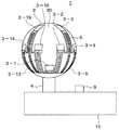
以下、第1実施形態について説明する。図1に示すように、風向風速計1は、車両10のエンジンルーム112内において、エンジン114の周囲に複数個配置される。これら風向風速計1は、すべて同等の構成を有している。以下、これらのうち1つの風向風速計1の構成について説明する。風向風速計1は、風状態計測装置に対応する。
(1st Embodiment)
Hereinafter, the first embodiment will be described. As shown in FIG. 1, a plurality of
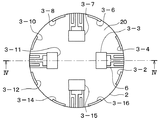
図2、図3、図4に示すように、1つの風向風速計1は、本体部20、16個の感温素子3−1、…、3−16、複数本の配線6、電源回路7、算出回路8、外気温センサ9、および収容ケース11を有している。風向風速計1は、風向風速計1の周囲を流れる風の向きおよび速さを計測し、計測結果を電気信号として出力する。本体部20は、熱伝導体2と、支柱4と、ヒータカバー31と、ヒータ32と、ヒータ温度センサ33とを有する。本体部20、感温素子3−1、…、3−16、配線6が、全体として、感温構造体に対応する。
As shown in FIGS. 2, 3, and 4, one
熱伝導体2は、計測すべき方位に対して断面形状が円形となる電気的絶縁体である。具体的には、熱伝導体2は、合成樹脂製の略球形状の、熱を伝導可能な筐体である。ただし、熱伝導体2の内部には、熱伝導体2の中心から熱伝導体2の表面まで柱状に伸びる孔37が形成されている。熱伝導体2に用いられる材料は、例えば、ポリアミドまたはPEEKである。PEEKは、ポリエーテルエーテルケトンの略である。
The
支柱4は、熱伝導体2の下端部に固定された中空の円筒形状の部材である。具体的には、支柱4は、図4に示すように、支柱4の内部空間である貫通孔41と熱伝導体2の孔37とが連通した状態で、熱伝導体2に固定されている。この固定により、支柱4は、熱伝導体2を支える機能を有する。支柱4の他端は収容ケース11に固定されている。支柱4の貫通孔41は収容ケース11の内部と連通している。
The
ヒータカバー31は、ヒータ32と、ヒータ温度センサ33を覆う樹脂製またはセラミック製の部材であり、孔37の内部に稠密に充填されている。したがって、ヒータ32、ヒータ温度センサ33およびヒータカバー31は、熱伝導体2の内部、具体的には孔37内に配置されている。また、ヒータ32は略球形状である熱伝導体2の中心部に位置し、ヒータ温度センサ33はヒータ32の近傍に配置されている。このように、孔37は、ヒータ32、ヒータ温度センサ33およびヒータカバー31を受け入れるために形成された孔である。
The
ヒータ32は、電源回路7から給電されることで発熱する。例えば、ヒータ32は、電熱線で構成されていてもよい。ヒータ32の発熱によって発生した熱は、熱伝導によりヒータカバー31、熱伝導体2をこの順に伝わり、熱伝導体2から感温素子3−1、…、3−16に熱伝導により伝わる。
The
16個の感温素子3−1、…、3−16は、図2、図3、図4に示すように、熱伝導体2の表面に分散して貼り付けられている。これにより、感温素子3−1、…、3−16は、裏面で熱伝導体2と接触すると共に、表面で熱伝導体2の周囲を流れる空気(すなわち外気)に接触する。したがって、感温素子3−1、…、3−16は、外気と熱伝導により熱交換することで、外気から熱的に影響を受ける。
The 16 thermosensitive elements 3-1,..., 3-16 are dispersed and attached to the surface of the
図2、図3に示すように、感温素子3−1、…、3−16の中心位置は、方位角が22.5度ずつずれて0°から337.5°まで等間隔で配置されている。また、図2、図3に示すように、感温素子3−1、…、3−16の中心位置の各々は、極角が−45°、0°、45°のいずれかに配置されており、かつ、方位角が隣り合う感温素子に対して極角が45度ずれて配置されている。また、中心位置の極角が−45°に配置されている感温素子と方位角が隣り合う2つの感温素子は、中心位置の極角が0°である。また、中心位置の極角が45°に配置されている感温素子と方位角が隣り合う2つの感温素子も、中心位置の極角が0°である。また、中心位置の極角が0°に配置されている感温素子と方位角が隣り合う2つの感温素子のうち、一方の感温素子の中心位置の極角が−45°であり、他方の感温素子の中心位置の極角が45°である。 As shown in FIGS. 2 and 3, the center positions of the temperature-sensitive elements 3-1,..., 3-16 are arranged at equal intervals from 0 ° to 337.5 ° with an azimuth shifted by 22.5 degrees. ing. Also, as shown in FIGS. 2 and 3, each of the center positions of the temperature sensing elements 3-1,..., 3-16 has a polar angle of -45 °, 0 °, or 45 °. In addition, the polar angle is shifted by 45 degrees with respect to the temperature sensing element whose azimuth angle is adjacent. The two temperature sensing elements whose azimuths are adjacent to the temperature sensing element whose central position has a polar angle of -45 ° have a central position of 0 °. Also, the two temperature sensing elements whose azimuth angles are adjacent to the temperature sensing element whose central position is disposed at a polar angle of 45 ° also have a central position of 0 °. In addition, the polar angle at the center position of one of the temperature sensing elements is −45 °, of the two temperature sensing elements adjacent to the azimuth and the temperature sensing element in which the polar angle at the center position is arranged at 0 °, The polar angle at the center position of the other temperature sensing element is 45 °.
より具体的には、感温素子3−1、3−5、3−9、3−13の各々は、中心位置の極角が−45°となる。また、感温素子3−2、3−4、3−6、3−8、3−10、3−12、3−14、3−16の各々は、中心位置の極角が0°となる。また、感温素子3−3、3−7、3−11、3−15の各々は、中心位置の極角が45°となる。 More specifically, in each of the temperature-sensitive elements 3-1, 3-5, 3-9, and 3-13, the polar angle at the center position is -45 degrees. In addition, each of the temperature sensing elements 3-2, 3-4, 3-6, 3-8, 3-10, 3-12, 3-14, and 3-16 has a polar angle of 0 ° at the center position. . Further, each of the temperature sensing elements 3-3, 3-7, 3-11, and 3-15 has a polar angle of 45 ° at the center position.
ここで、極角および方位角は、熱伝導体2の中心を中心とする球面座標表示における極角θおよび方位角φである。より具体的には、ある方向の極角は、その方向とz軸方向が成す角度であり、その方向の方位角は、その方向をx−y平面に射影した方向とx軸方向とが成す角度である。本実施形態では、z軸は、熱伝導体2の中心を通り、図2中上下方向に伸びる軸であり、x軸は当該中心を通りz軸に直交する軸であり、y軸は当該中心を通りz軸およびx軸に直交する軸である。また、x−y平面は、x軸とy軸とを含む平面である。
Here, the polar angle and the azimuth are the polar angle θ and the azimuth φ in spherical coordinate display centering on the center of the
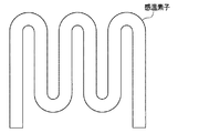
感温素子3−1、…、3−16の各々は、図5に示すように蛇行しながら一端から他端まで伸びている。感温素子3−1、…、3−16の各々は、図6に示すように熱伝導体2の表面上に形成された分子接合層101と、分子接合層101上に形成された導電材層102と、導電材層102の上に形成された金属層103とからなる層構造を有している。なお、分子接合層101、導電材層102および金属層103の詳細については後述する。
Each of the temperature sensing elements 3-1,..., 3-16 extends from one end to the other end while meandering as shown in FIG. Each of the temperature sensing elements 3-1,..., 3-16 has a
感温素子3−1、…、3−16の各々は、通電されると発熱する電気抵抗であるが、その発熱量は、ヒータ32の発熱量に比べると無視できるほど小さい。したがって、感温素子3−1、…、3−16は、熱伝導体2の周囲を流れる空気以外に由来して当該空気から伝わる熱以外の熱によって、具体的には、ヒータ32によって生成されてヒータカバー31、熱伝導体2を伝導した熱によって、温度上昇する。感温素子3−1、…、3−16に用いられる金属は、温度が上昇するにつれて電気抵抗値(以下、単に抵抗値ともいう)が増大する。つまり、感温素子3−1、…、3−16は、自己の温度に応じて電気的特性すなわち抵抗値が変化する。例えば、感温素子3−1、…、3−16は、温度が上昇すると抵抗値が高くなる。
Each of the temperature sensing elements 3-1,..., 3-16 is an electric resistance that generates heat when energized, but the amount of heat generated is negligibly small compared to the amount of heat generated by the
図2、図3、図7に示すように、配線6は感温素子3−1、…、3−16を直列に接続すると共に、感温素子3−1、…、3−16の各々を算出回路8に接続する導線である。配線6の一部は、感温素子3−1、…、3−16の両端から伸びて熱伝導体2の表面に配置され、熱伝導体2の表面に沿って伸びる。配線6の残りの一部は、図4に示すように、熱伝導体2と支柱4の隙間から熱伝導体2の内部に入り、支柱4の貫通孔41を経て収容ケース11の内部に引き込まれている。収容ケース11の内部には算出回路8が収容されており、配線6は算出回路8に接続されている。
As shown in FIGS. 2, 3, and 7, the
外気温センサ9は、本体部20の近傍に配置され、収容ケース11の外面に取り付けられている。外気温センサ9は、エンジンルーム112内かつ本体部20の周囲の空気の温度(すなわち外気温)に応じた電気信号を算出回路8に出力するセンサである。
The outside air temperature sensor 9 is arranged near the
ヒータ温度センサ33は、ヒータ32の近傍に配置されているため、ヒータ32の温度に応じた電気信号を出力できる。このヒータ温度センサ33の電気信号も算出回路8に入力される。
Since the
電源回路7はヒータ32に給電するための回路基板であり、収容ケース11に収容されている。電源回路7とヒータ32とは給電ケーブル34を用いて接続されている。電源回路7はヒータ32に給電する電力を変化させることにより、ヒータ32の発熱量を変化させることができる。言うまでもないが、給電しないことすなわちヒータ32の発熱量を0とすることも可能である。電源回路7は算出回路8に接続されており、算出回路8による制御を受ける。
The
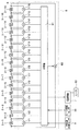
算出回路8は、図7に示すように、16個の電圧計V1、…、V16、処理部81、電流源82を有している。電圧計V1、…、V16は、感温素子3−1、…、3−16に、この順に一対一に対応している。電圧計V1、…、V16の各々から、対応する感温素子の両端間の電圧に応じた信号が、処理部81に入力される。
As shown in FIG. 7, the
このように、電圧計V1、…、V16の各々は、対応する感温素子に及ぼされる電流および電圧のうち一方の電気的物理量(すなわち電圧)を検出する電気的物理量計である。そして、電流源82は、感温素子3−1、…、3−16に及ぼされる電流および電圧のうち上記一方の電気的物理量(すなわち電圧)とは異なる他方の電気的物理量(すなわち電流)を制御する電源である。
Thus, each of the voltmeters V1,..., V16 is an electrical physical quantity meter that detects one electrical physical quantity (ie, voltage) of the current and the voltage applied to the corresponding temperature-sensitive element. The
処理部81は、CPU、RAM、ROM等を備えた周知のマイクロコンピュータである。CPUは、ROMに記録されたプログラムを実行し、その際にRAMを作業領域として使用する。CPUがプログラムを実行することにより、処理部81が後述する種々の処理を実行する。
The
電流源82は、感温素子3−1、…、3−16に所定の電流を供給する回路である。電流源82から供給される電流の電流値は、処理部81によって制御可能となっている。
The
収容ケース11は、上述のように電源回路7および算出回路8を収容するとともに本体部20および外気温センサ9を保持している。そして、収容ケース11は、風向風速計1をエンジンルーム112に取り付けるためにも使用されている。
The
以上のような構成の風向風速計1の作動について、以下説明する。算出回路8の処理部81は、感温素子3−1、…、3−16に所定の一定電流値の電流が供給されるよう、電流源82を制御する。これにより、電流源82は、一定の電流値の電流を感温素子3−1、…、3−16に供給する。
The operation of the
また、処理部81は、上述のように電流源82を制御している期間中に、電圧計V1、…、V16から入力された信号に基づいて、感温素子3−1、…、3−16の両端に印加された16個の電圧値を繰り返し定期的に(例えば1秒に1回)特定する。
Further, the
そして処理部81は、16個の電圧値を特定する度に、これら電圧値に基づいて、感温素子3−1、…、3−16の各々の温度を特定する。具体的には、処理部81は、感温素子3−1、…、3−16の各々について、当該感温素子の両端に印加された電圧値と、上述の一定電流値に基づいて、当該感温素子の抵抗値を算出する。そして処理部81は、算出した抵抗値を、ROMにあらかじめ記録されている抵抗値−温度テーブルに適用することで、当該感温素子が当該抵抗値を示すときの当該感温素子の温度を特定する。抵抗値−温度テーブルは、抵抗値と、感温素子3−1、…、3−16が当該抵抗値を示すときの当該感温素子の温度との対応関係を表すデータである。
Each time the
また処理部81は、感温素子3−1、…、3−16の各々の温度を特定する度に、外気温センサ9からの信号に基づいて外気温を特定し、特定した外気温と感温素子3−1、…、3−16の温度に基づいて、風向および風速を算出する。
The
具体的には、処理部81は、感温素子3−1、…、3−16の温度の平均値を算出し、算出した平均値と外気温との差の絶対値が大きいほど風速が大きくなるよう、風速を決定する。
Specifically, the
また、処理部81は、感温素子3−1、…、3−16の周囲の風向を、以下のような方法で導出する。処理部81は、まず、16個の感温素子3−1、…、3−16の温度のうち、低いものから順に5個の温度Tx1、Tx2、Tx3、Tx4、Tx5を抽出する。ここでは、温度Tx1、Tx2、Tx3、Tx4、T5は少なくとも1つの値(例えばすべての値)が異なる値であるとする。
The
続いて処理部81は、抽出した5つの温度に基づいて、風向を算出する。算出方法は、感温素子3−1、…、3−16の各々の温度Tsが以下の式(1)のように極角θ、方位角φの関数で近似されることを利用する。
Ts=a×θ2+b×φ2+c×θ+d×φ+e (1)
ここで、Tsは、対象となる感温素子の温度、θおよびφは当該感温素子の中心位置の極角および方位角である。またa、b、c、d、eは定数である。
Subsequently, the
Ts = a × θ 2 + b × φ 2 + c × θ + d × φ + e (1)
Here, Ts is the temperature of the target thermosensitive element, and θ and φ are the polar angle and azimuth of the center position of the thermosensitive element. A, b, c, d, and e are constants.
具体的には、処理部81は、温度Tx1、Tx2、Tx3、Tx4、Tx5を示した感温素子について、温度、中心位置の極角、中心位置の方位角の3つの値を上記式(1)に代入する。それにより、a、b、c、d、eに関する5つの連立方程式(2)、(3)、(4)、(5)、(6)を得る。
Tx1=a×θ12+b×φ12+c×θ1+d×φ1+e (2)
Tx2=a×θ22+b×φ22+c×θ2+d×φ2+e (3)
Tx3=a×θ32+b×φ32+c×θ3+d×φ3+e (4)
Tx4=a×θ42+b×φ42+c×θ4+d×φ4+e (5)
Tx5=a×θ52+b×φ52+c×θ5+d×φ5+e (6)
処理部81は、この連立方程式を解いてa、b、c、d、eを算出する。そして、算出したa、b、c、d、eを式(1)に代入し、更に式(1)の1階全微分がゼロになるθ、φを算出する。処理部81は、算出したθ、φの位置から熱伝導体2の中心に向かう方向を、風向として決定する。
Specifically, the
Tx1 = a × θ1 2 + b × φ1 2 + c × θ1 + d × φ1 + e (2)
Tx2 = a × θ2 2 + b ×
Tx3 = a × θ3 2 + b ×
Tx4 = a × θ4 2 + b ×
Tx5 = a × θ5 2 + b × φ5 2 + c × θ5 + d × φ5 + e (6)
The
(感温素子の詳細)
感温素子3−1、…、3−16の各々は、上述したように分子接合層101、導電材層102および金属層103の層構造を有している。その層構造の詳細について、製造工程に従って説明する。
(Details of temperature sensing element)
Each of the temperature sensing elements 3-1,..., 3-16 has a layer structure of the
図8に示すように、感温素子3−1、…、3−16の製造工程は、合成樹脂の洗浄、分子接合層の形成、触媒の付与、導電材層の形成、金属層の形成という各工程からなる。 As shown in FIG. 8, the manufacturing steps of the temperature-sensitive elements 3-1,..., 3-16 include washing of a synthetic resin, formation of a molecular bonding layer, application of a catalyst, formation of a conductive material layer, and formation of a metal layer. It consists of each process.
合成樹脂の洗浄工程は、ステップS1、S2、S3を有する。先ずステップS1で、熱伝導体2を構成している合成樹脂(PEEK)の加工応力除去として、熱伝導体2を150℃にて5分間保持する。次にステップS2で、アセトンを用いた超音波洗浄を10分間行うことで、熱伝導体2の表面の脱脂を行う。そしてステップS3で、コロナ放電処理により熱伝導体2の表面を改質する。
The synthetic resin cleaning step includes steps S1, S2, and S3. First, in step S1, the
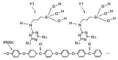
続く分子接合層の形成工程では、ステップS4で、熱伝導体2の表面に、分子接合層を構成するための有機化合物を化学的に結合させる処理が行われる。本実施形態においては、図9に示す構造の有機化合物Y1を溶質としている有機溶剤中に熱伝導体2を浸漬し、上記改質された熱伝導体2の表面に有機化合物Y1を吸着させた後、熱伝導体2を引き揚げて乾燥させる。
In the subsequent step of forming the molecular bonding layer, in step S4, a process of chemically bonding an organic compound for forming the molecular bonding layer to the surface of the
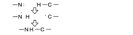
ステップS4では次に、その熱伝導体2の表面に紫外線を照射する。すると、図10に示すように、アジド基に紫外線Hνが当たることで、有機化合物Y1のアジド基の一部からN2が遊離しナイトレンが形成される。そして、図11に示すように、そのナイトレンが、PEEK中のC−H結合の水素を引き剥がして当該水素に結合し、さらに、そのナイトレンの余った電子と炭素の電子が対となって共有結合する。すなわちCH挿入反応が起こる。ナイトレンの反応性が強いので、樹脂内にあるすべてのCH結合が選択対象になる。この反応によって、図12に示すように、PEEKのベンゼン環の一部と有機化合物Y1とが結合する。その結果、熱伝導体2の表面に有機化合物Y1による分子接合層101が形成される。
In step S4, the surface of the
次の触媒の付与工程はステップS5、S6を有する。ステップS5では、触媒としてのパラジウム(Pd)を分子接合層101の有機化合物Y1に結合させるために、熱伝導体2を塩化パラジウム(PdCl2)の水溶液に1分間浸漬する。続くステップS6では、有機化合物Y1とパラジウムとの結合促進を目的として、パラジウムの水溶液から取り出した熱伝導体2を150℃にて5分間保持する。この工程を経ることにより、図13に示すように有機化合物Y1のトリアジン環の窒素原子が電子対を供与してパラジウムと配位結合し、ヒドロキシ基の水素との置換にてパラジウムがイオン結合する。このパラジウムの付与は次の導電材層の形成工程での反応性を上げるために行われる。
The next catalyst application step has steps S5 and S6. In step S5, the
その導電材層の形成工程はステップS7、S8を有する。ステップS7では、分子接合層101上に導電材層102を形成するために熱伝導体2をめっき液に浸漬して無電解ニッケルホウ素めっきを行う。
The conductive material layer forming step includes steps S7 and S8. In step S7, in order to form the
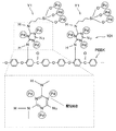
この無電解ニッケルホウ素めっきでは、先ず下記の化学式(8)に示す反応により、めっき液のニッケル(Ni)が、触媒の付与工程で有機化合物Y1に付与されたパラジウムに替わって、図14に示すように有機化合物Y1に結合する。すなわち、トリアジン環の窒素原子が電子対を供与してニッケルと配位結合し、ヒドロキシ基の水素と置換した形態でニッケルがイオン結合する。
Pd+Ni2+→Pd2++Ni (8)
ステップS7では続いて、有機化合物Y1に結合したニッケルを起点として、ニッケルとホウ素化ニッケルが析出し、導電材層102となる皮膜を形成する。その析出反応は下記の化学式(9)、(10)、(11)に示す反応によってなされる。
3Ni2++(CH3)2NHBH3+H2O→3Ni+H3BO3+(CH3)2H2N++5H+ (9)
4Ni2++2(CH3)2NHBH3+3H2O→2Ni+NiB+H3BO3+2HN++6H+ (10)
(CH3)2NHBH3+3H2O→H3BO3+(CH3)2H2N++3H2 (11)
すると、図15に示すように、ニッケルとホウ素化ニッケルにて形成された導電材層102の内部に有機化合物Y1が入り込んだ構造が生じる。この有機化合物Y1の入り込み、化学的に結合することで分子接合層101と導電材層102とが強固に接合する。(10)の反応によって生成されるホウ素化ニッケルは不純物である。このような不純物がニッケル等の金属に含まれていると、当該金属の電気抵抗率の温度係数が低下する。すなわち、単位温度変化量あたりの電気抵抗値の変化量の絶対値が低下する。無電解ニッケルホウ素めっきが済んだ後は、ステップS8で、熱伝導体2をめっき液から揚げて、めっきに伴う残留応力を除去するために150℃にて5分間保持する。
In this electroless nickel-boron plating, first, nickel (Ni) in the plating solution is replaced by palladium applied to the organic compound Y1 in the catalyst applying step by a reaction represented by the following chemical formula (8), and is shown in FIG. To organic compound Y1 as described above. That is, the nitrogen atom of the triazine ring donates an electron pair to form a coordinate bond with nickel, and forms an ion bond with nickel in a form in which it is substituted with hydrogen of a hydroxy group.
Pd + Ni 2+ → Pd 2+ + Ni (8)
In step S7, nickel and nickel boride are deposited starting from nickel bonded to the organic compound Y1 to form a film to be the
3Ni 2+ + (CH 3 ) 2 NHBH 3 + H 2 O → 3Ni + H 3 BO 3 + (CH 3 ) 2 H 2 N + + 5H + (9)
4Ni 2+ +2 (CH 3 ) 2 NHBH 3 + 3H 2 O → 2Ni + NiB + H 3 BO 3 + 2HN + + 6H + (10)
(CH 3 ) 2 NHBH 3 + 3H 2 O → H 3 BO 3 + (CH 3 ) 2 H 2 N + + 3H 2 (11)
Then, as shown in FIG. 15, a structure is generated in which the organic compound Y1 enters the inside of the
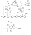
次の金属層の形成工程は、ステップS9を含む。ステップS9では、電気ニッケルめっきによって導電材層102上にニッケルの皮膜である金属層103を形成する。この電気ニッケルめっきは、図16に示すように、電解液には硫酸ニッケル(NiSO4)水溶液を使用し、熱伝導体2に形成された導電材層102を陰極、ニッケル板を陽極として行われる。これにより、図17に示すように、導電材層102上にニッケルが析出し金属層103を形成する。陰極となる導電材層102上にはニッケルのみが析出するので、金属層103となる被膜には不純物が含まれない。すなわち、金属層103は導電材層102よりもニッケルの純度が高い。電気ニッケルめっきにて導電材層102上に金属層103を形成するので、両者の接合は強固なものになる。
The next step of forming a metal layer includes step S9. In step S9, a
こうした工程を経ることにより、熱伝導体2の表面に分子接合層101、導電材層102および金属層103の層構造が形成される。そして、感温素子3−1、…、3−16となるパターン(図5参照)および配線6となるパターンが残るように、熱伝導体2の表面部分をエッチング処理することで、図2、図3に示す通りの感温素子3−1、…、3−16および配線6が熱伝導体2の表面に設けられる。
Through these steps, a layer structure of the
上記の通り、熱伝導体2の表面を構成する合成樹脂(PEEK)と分子接合層101の有機化合物Y1とが化学的に結合しているため、この両者間の接合は強固である。その分子接合層101の上に無電解めっきにより導電材層102が形成されているが、導電材層102の内部に有機化合物Y1が入り込み、配位結合、イオン結合によって分子接合層101と導電材層102とが強固に接合している。さらに、導電材層102の上に電気めっきにて金属層103を形成しているので、導電材層102と金属層103との接合は強固なものになっている。
As described above, since the synthetic resin (PEEK) constituting the surface of the
また、熱伝導体2の表面に配された配線6も、感温素子3−1、…、3−16と同工程で設けられ、感温素子3−1、…、3−16と同じ層構造を有するので、熱伝導体2と配線6との密着性も良好、確実である。
The
さて、感温素子3−1、…、3−16において単に導電性のみを要するのであれば、導電材層102のみにて十分といえる。しかしながら、本実施形態にあっては導電材層102の上に金属層103を設けている。その理由は以下の通りである。
By the way, if the temperature-sensitive elements 3-1,..., 3-16 need only conductivity, it can be said that only the
導電材層102を形成するための無電解ニッケルホウ素めっきの説明で述べ、図15にも示したように、無電解ニッケルホウ素めっきでは、ニッケルだけでなくホウ素化ニッケルも析出し、導電材層102となる皮膜中に残留する。導電材層102中に不純物としてホウ素が存在すると、導電材層102の電気抵抗率の温度係数が小さい。そのため、温度が上昇するにつれて電気抵抗値が増大するという、感温素子3−1、…、3−16に要求される特性を満たすことができない場合がある。つまり、導電材層102のみで金属層103を有さない構成であっては、感温素子3−1、…、3−16としての機能が金属層103を有する構成に比べて低い。
As described in the description of electroless nickel-boron plating for forming the
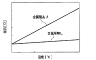
そこで、本実施形態にあっては導電材層102の上に、ニッケルの純度が導電材層102よりも高い金属層103を設けている。これにより、導電材層102の上に、電気抵抗率の温度係数が導電材層102の電気抵抗率の温度係数よりも大きい、金属層103が設けられる。その効果は図18、図19に示す通りであり、金属層103を設けた方が温度係数が大きく、感温素子の温度上昇に伴って抵抗値が増加する変化率も十分に大きい。このように、金属層103を設けたことで、感温素子3−1、…、3−16に要求される電気的特性を満たしている。
Therefore, in this embodiment, a
(他の実施形態)
なお、本発明は上記した実施形態に限定されるものではなく、特許請求の範囲に記載した範囲内において適宜変更が可能である。また、また、上記実施形態において、実施形態を構成する要素は、特に必須であると明示した場合および原理的に明らかに必須であると考えられる場合等を除き、必ずしも必須のものではない。また、上記実施形態において、実施形態の構成要素の個数、数値、量、範囲等の数値が言及されている場合、特に必須であると明示した場合および原理的に明らかに特定の数に限定される場合等を除き、その特定の数に限定されるものではない。特に、ある量について複数個の値が例示されている場合、特に別記した場合および原理的に明らかに不可能な場合を除き、それら複数個の値の間の値を採用することも可能である。また、上記実施形態において、構成要素等の形状、位置関係等に言及するときは、特に明示した場合および原理的に特定の形状、位置関係等に限定される場合等を除き、その形状、位置関係等に限定されるものではない。また、本発明は、上記実施形態に対する以下のような変形例も許容される。なお、以下の変形例は、それぞれ独立に、上記実施形態に適用および不適用を選択できる。すなわち、以下の変形例のうち明らかに矛盾する組み合わせを除く任意の組み合わせを、上記実施形態に適用することができる。
(Other embodiments)
Note that the present invention is not limited to the above-described embodiment, and can be appropriately changed within the scope described in the claims. In addition, in the above-described embodiment, elements constituting the embodiment are not necessarily essential, unless explicitly stated as essential, or considered to be indispensable in principle. Further, in the above embodiment, when numerical values such as the number, numerical value, amount, range, etc. of the constituent elements of the exemplary embodiment are mentioned, it is particularly limited to a specific number, if it is clearly stated that it is essential, and it is clearly limited to a specific number in principle. However, the number is not limited to that specific number except in the case where the In particular, when a plurality of values are exemplified for a certain amount, it is also possible to adopt a value between the plurality of values, unless otherwise specified and unless it is clearly impossible in principle. . Further, in the above-described embodiment, when referring to the shape, positional relationship, and the like of the components, the shape, position, etc., unless otherwise specified, and in principle, the shape, the positional relationship, etc. are limited. It is not limited to the relationship. Further, the present invention allows the following modifications to the above embodiment. The following modifications can be independently applied or not applied to the above embodiment. That is, any combination of the following modified examples except for a contradictory combination can be applied to the above embodiment.
(感温素子のパターンの変形例)
感温素子3−1、…、3−16のパターンとして、上記実施形態では規矩状に蛇行する形態を示しているが、以下の各例のような変形例も可能である。
(Modification of pattern of thermosensitive element)
The pattern of the temperature-sensitive elements 3-1,..., 3-16 has a meandering shape in a regular rectangular shape in the above embodiment, but modifications such as the following examples are also possible.
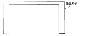
まず、図20に示すようにコの字状のパターンにすることもできる。このようなパターンであると形成が容易であり、また直線部の長手方向の応力に対して耐性が高い。 First, a U-shaped pattern can be used as shown in FIG. Such a pattern is easy to form and has high resistance to the stress in the longitudinal direction of the linear portion.
また、実施形態と同様に蛇行する形態であっても、図21に示すように折り返し部分を円弧状にすることもできる。実施形態も本変形例も感温素子としての回路長を長くして抵抗値を大きくできる点は同じであるが、本変形例は折り返し部分を円弧状にしたので応力が集中し難いという利点がある。 Further, even in a meandering form as in the embodiment, the folded portion may be formed in an arc shape as shown in FIG. Both the embodiment and the present modification have the same point that the resistance value can be increased by increasing the circuit length as a temperature sensing element, but the present modification has an advantage that stress is hardly concentrated because the folded portion has an arc shape. is there.
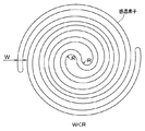
或いは、図22、図23に示すように渦巻き状にすることも可能である。渦巻き状にすると、回路長を長くして抵抗値を大きくでき、全体的に応力が集中し難くなる。特に、図23の例のように、渦巻きの中心部の円弧の内径Rが線幅Wよりも大きい構成にすると、中心部での2つの渦線の接続が滑らかになり、この部分での応力の集中を避けることができる。
(表面保護の変形例)
上記実施形態では感温素子3−1、…、3−16の表面は金属層103、つまりニッケルである。ニッケル自体も錆に対する耐性はあるものの、例えば、金や白金などの貴金属層を金属層103に積層して防錆効果を高めることができる。この構成は、金属層103が耐錆性に優れない金属の場合には特に有効である。
Alternatively, it is also possible to form a spiral as shown in FIGS. When the shape is spiral, the circuit length can be increased and the resistance value can be increased, and it is difficult to concentrate stress as a whole. In particular, when the inner diameter R of the circular arc at the center of the spiral is larger than the line width W as in the example of FIG. 23, the connection between the two spiral lines at the center becomes smooth, and the stress at this portion is reduced. Concentration can be avoided.
(Modification of surface protection)
In the above embodiment, the surfaces of the temperature-sensitive elements 3-1,..., 3-16 are the
また、感温素子の表面を、或いは熱伝導体2の表面全域を、非金属の絶縁体膜によって被覆することも可能である。こうした被覆により異物との接触などによる損傷を防止できる。
(分子接合層を構成する有機化合物)
実施形態では図9に構造式を示す有機化合物Y1を用いているが、実施形態における説明からも明らかなとおり、
(1)ナイトレンを生じて合成樹脂中の炭素と結合するためのアジド基、
(2)金属原子と配位結合するためのトリアジン環、
(3)金属原子とイオン結合するためのヒドロキシ基またはヒドロキシ基を保持する基を有する有機化合物であればよく、具体的には、以下の一般式(g)で表される構造の有機化合物であれば採用できる。
It is also possible to cover the surface of the temperature-sensitive element or the entire surface of the
(Organic compound constituting molecular bonding layer)
In the embodiment, the organic compound Y1 having the structural formula shown in FIG. 9 is used. However, as is clear from the description of the embodiment,
(1) an azide group for generating nitrene and bonding to carbon in the synthetic resin;
(2) a triazine ring for coordinating with a metal atom,
(3) Any organic compound having a hydroxy group for forming an ionic bond with a metal atom or a group holding a hydroxy group may be used, and specifically, an organic compound having a structure represented by the following general formula (g) If you can, you can adopt it.
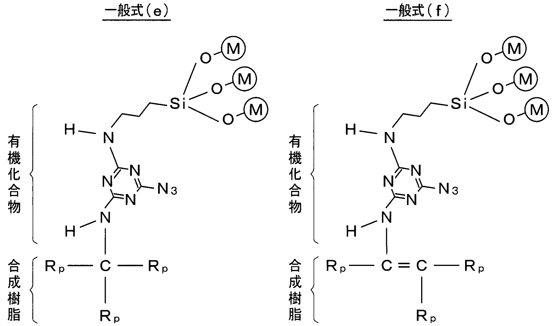
ただし、この化学式中、Eは任意の基であり、Fはヒドロキシ基またはヒドロキシ基を併せ持った基である。Qは、N3またはNR1(R2)である。R1、R2 は、H、炭素数が1以上24以下の炭化水素基、または−RSi(R’)n(OA)3−nである。Rは炭素数が1以上12以下の鎖状の炭化水素基で、R’は炭素数が1以上4以下の鎖状の炭化水素基である。Aは、Hまたは炭素数が1以上4以下の鎖状の炭化水素基である。nは0以上2以下の整数である。R1とR2 とは同一でも異なるものでもよい。)
この一般式(g)で表す有機化合物を用いた場合、合成樹脂と分子接合層を構成する有機化合物との化学的な結合の構造は、以下の一般式(a)または一般式(b)で表される構造となる。その場合も、合成樹脂と分子接合層の有機化合物とが化学的に結合するため、この両者間の接合は強固である。
However, in this chemical formula, E is an arbitrary group, and F is a hydroxy group or a group having both hydroxy groups. Q is N 3 or NR 1 (R 2 ). R 1 and R 2 are H, a hydrocarbon group having 1 to 24 carbon atoms, or —RSi (R ′) n (OA) 3-n . R is a chain hydrocarbon group having 1 to 12 carbon atoms, and R 'is a chain hydrocarbon group having 1 to 4 carbon atoms. A is H or a chain hydrocarbon group having 1 to 4 carbon atoms. n is an integer of 0 or more and 2 or less. R 1 and R 2 may be the same or different. )
When the organic compound represented by the general formula (g) is used, the structure of the chemical bond between the synthetic resin and the organic compound constituting the molecular bonding layer is represented by the following general formula (a) or general formula (b). It will be the structure shown. Also in this case, since the synthetic resin and the organic compound of the molecular bonding layer are chemically bonded, the bonding between the two is strong.
ただし、この化学式中、Eは任意の基であり、Fはヒドロキシ基またはヒドロキシ基を併せ持った基である。Qは、N3またはNR1(R2)である。R1、R2 は、H、炭素数が1以上24以下の炭化水素基、または−RSi(R’)n(OA)3−nである。Rは炭素数が1以上12以下の鎖状の炭化水素基である。R’は炭素数が1以上4以下の鎖状の炭化水素基である。Aは、Hまたは炭素数が1以上4以下の鎖状の炭化水素基である。nは0以上2以下の整数である。R1とR2とは同一でも異なるものでもよい。Rpは前記合成樹脂を構成する高分子化合物中で、前記分子接合層の有機化合物と結合した炭素につながる高分子化合物である。 However, in this chemical formula, E is an arbitrary group, and F is a hydroxy group or a group having both hydroxy groups. Q is N 3 or NR 1 (R 2 ). R 1 and R 2 are H, a hydrocarbon group having 1 to 24 carbon atoms, or —RSi (R ′) n (OA) 3-n . R is a chain hydrocarbon group having 1 to 12 carbon atoms. R ′ is a chain hydrocarbon group having 1 to 4 carbon atoms. A is H or a chain hydrocarbon group having 1 to 4 carbon atoms. n is an integer of 0 or more and 2 or less. R 1 and R 2 may be the same or different. R p is a polymer compound that is connected to carbon bonded to the organic compound of the molecular bonding layer in the polymer compound constituting the synthetic resin.
また、導電材層の金属原子と分子接合層を構成する有機化合物とは、以下の一般式(c)または一般式(d)に表す通り、トリアジン環の窒素原子と導電材層の金属原子とが配位結合しているだけでも、導電材層と分子接合層との接合強さは十分で、実施形態と同等の効果が得られる。 In addition, the metal atom of the conductive material layer and the organic compound forming the molecular bonding layer are, as shown in the following general formula (c) or (d), a nitrogen atom of a triazine ring and a metal atom of the conductive material layer. Is coordinated only, the bonding strength between the conductive material layer and the molecular bonding layer is sufficient, and an effect equivalent to that of the embodiment can be obtained.
ただし、この化学式中、Eは任意の基であり、Fはヒドロキシ基またはヒドロキシ基を併せ持った基である。Qは、N3またはNR1(R2)である。R1、R2 は、H、炭素数が1以上24以下の炭化水素基、または−RSi(R’)n(OA)3−nである。Rは炭素数が1以上12以下の鎖状の炭化水素基である。R’は炭素数が1以上4以下の鎖状の炭化水素基である。Aは、Hまたは炭素数が1以上4以下の鎖状の炭化水素基である。nは0以上2以下の整数である。R1とR2 とは同一でも異なるものでもよい。Mは金属原子である。Rpは前記合成樹脂を構成する高分子化合物中で、前記分子接合層の有機化合物と結合した炭素につながる高分子化合物である。 However, in this chemical formula, E is an arbitrary group, and F is a hydroxy group or a group having both hydroxy groups. Q is N 3 or NR 1 (R 2 ). R 1 and R 2 are H, a hydrocarbon group having 1 to 24 carbon atoms, or —RSi (R ′) n (OA) 3-n . R is a chain hydrocarbon group having 1 to 12 carbon atoms. R ′ is a chain hydrocarbon group having 1 to 4 carbon atoms. A is H or a chain hydrocarbon group having 1 to 4 carbon atoms. n is an integer of 0 or more and 2 or less. R 1 and R 2 may be the same or different. M is a metal atom. R p is a polymer compound that is connected to carbon bonded to the organic compound of the molecular bonding layer in the polymer compound constituting the synthetic resin.
或いは、以下の一般式(d)または一般式(e)に表すように、ヒドロキシシリル基の水素との置換にて金属原子(実施形態ではニッケル)がイオン結合するだけであっても、導電材層と分子接合層との接合強さは十分で、実施形態と同等の効果が得られる。 Alternatively, as shown in the following general formula (d) or general formula (e), even if a metal atom (nickel in the embodiment) is only ion-bonded by replacement of the hydroxysilyl group with hydrogen, the conductive material The bonding strength between the layer and the molecular bonding layer is sufficient, and the same effect as in the embodiment can be obtained.
この化学式中、Eは任意の基であり、Fはヒドロキシ基またはヒドロキシ基を併せ持った基である。Qは、N3またはNR1(R2)である。R1、R2 は、H、炭素数が1以上24以下の炭化水素基、または−RSi(R’)n(OA)3−nである。Rは炭素数が1以上12以下の鎖状の炭化水素基である。R’は炭素数が1以上4以下の鎖状の炭化水素基である。Aは、Hまたは炭素数が1以上4以下の鎖状の炭化水素基である。nは0以上2以下の整数である。R1とR2 とは同一でも異なるものでもよい。Mは金属原子である。Rpは前記合成樹脂を構成する高分子化合物中で、前記分子接合層の有機化合物と結合した炭素につながる高分子化合物である。 In this formula, E is an arbitrary group, and F is a hydroxy group or a group having both hydroxy groups. Q is N 3 or NR 1 (R 2 ). R 1 and R 2 are H, a hydrocarbon group having 1 to 24 carbon atoms, or —RSi (R ′) n (OA) 3-n . R is a chain hydrocarbon group having 1 to 12 carbon atoms. R ′ is a chain hydrocarbon group having 1 to 4 carbon atoms. A is H or a chain hydrocarbon group having 1 to 4 carbon atoms. n is an integer of 0 or more and 2 or less. R 1 and R 2 may be the same or different. M is a metal atom. R p is a polymer compound that is connected to carbon bonded to the organic compound of the molecular bonding layer in the polymer compound constituting the synthetic resin.
言うまでもないが、実施形態のようにトリアジン環の窒素原子と導電材層の金属原子とが配位結合しており、かつヒドロキシ基またはヒドロキシ基を併せ持った基の水素との置換にて金属原子(実施形態ではニッケル)がイオン結合している構造であると、導電材層と分子接合層との接合強さは極めて良好である。 Needless to say, as in the embodiment, the nitrogen atom of the triazine ring and the metal atom of the conductive material layer are coordinate-bonded, and the metal atom ( When the structure is such that nickel (in the embodiment, nickel) is ion-bonded, the bonding strength between the conductive material layer and the molecular bonding layer is extremely good.
なお、有機化合物と結合する導電材層の金属原子は、実施形態で示したニッケルに限るものではない。分子接合層上に導電材層を形成する手法も、無電解めっきに限るものではない。 Note that the metal atom of the conductive material layer that bonds to the organic compound is not limited to nickel shown in the embodiment. The method of forming the conductive material layer on the molecular bonding layer is not limited to electroless plating.
また、分子接合層を構成する有機化合物と結合する合成樹脂としてPEEKを示したが、これに限るものではない。実施形態では有機化合物Y1とベンゼン環の炭素とが結合する例を示したが、有機化合物が結合する相手方の炭素はベンゼン環の炭素に限るものではなく、6員環以外の環に含まれる炭素であってもよいし、鎖状構造の中の炭素であってもよい。 Further, PEEK is shown as a synthetic resin that binds to the organic compound constituting the molecular bonding layer, but is not limited thereto. In the embodiment, the example in which the organic compound Y1 and the carbon of the benzene ring are bonded is shown. However, the carbon to which the organic compound is bonded is not limited to the carbon of the benzene ring. Or carbon in a chain structure.
また、上記実施形態において、導電材層102を分子接合層101に接合させる場合に、不純物としてホウ素化ニッケルが例示されている。しかし、導電材層102を分子接合層101に接合させる場合に不純物として残留し、導電材層102の電気抵抗率の温度係数を低下させるものは、ホウ素化ニッケルに限らない。例えば、導電材層102を分子接合層101の組成によっては、リンも同様の不純物として残留する場合がある。
In the above embodiment, nickel boride is exemplified as an impurity when the
また、上記実施形態における感温素子3−1、…、3−16は、自己の温度が上昇すると電気抵抗値が上昇するが、自己の温度が上昇すると電気抵抗値が下降するようになっていてもよい。 Further, the temperature-sensitive elements 3-1,..., 3-16 in the above embodiment increase in electrical resistance when their temperature rises, but decrease in electrical resistance when their temperature rises. You may.
感温素子3−1、…、3−16の各々は、通電されると発熱する電気抵抗であるが、その発熱量は、ヒータ32の発熱量に比べると無視できるほど小さい。したがって、感温素子3−1、…、3−16は、熱伝導体2の周囲を流れる空気以外に由来して当該空気から伝わる熱以外の熱によって、具体的には、ヒータ32によって生成されてヒータカバー31、熱伝導体2を伝導した熱によって、温度上昇する。感温素子3−1、…、3−16に用いられる金属は、温度が上昇するにつれて電気抵抗値(以下、単に抵抗値ともいう)が増大する。つまり、感温素子3−1、…、3−16は、自己の温度に応じて電気的特性すなわち抵抗値が変化する。例えば、感温素子3−1、…、3−16は、温度が上昇すると抵抗値が高くなる。
Each of the temperature sensing elements 3-1,..., 3-16 is an electric resistance that generates heat when energized, but the amount of heat generated is negligibly small compared to the amount of heat generated by the
また、上記実施形態における算出回路8の処理部81は、風向と風速の両方を算出するようになっているが、風向のみを算出してもよいし、風速のみを算出してもよい。
Further, the
また、処理部81は、感温素子3−1、…、3−16の抵抗値から温度を算出し、算出した温度の平均値と外気温の差から風速を算出している。しかし、必ずしもこのようになっていなくてもよい。例えば、処理部81は、抵抗値感温素子3−1、…、3−16の温度の平均値と外気温の差が一定になるようにヒータ32の温度をフィードバック制御し、そのヒータ32の発熱量に応じて風速を算出してもよい。その場合でも、処理部81は、感温素子3−1、…、3−16の電気抵抗値に応じてヒータ32への通電量を制御しているので、感温素子3−1、…、3−16の電気抵抗値に応じて風速算出することに変わりはない。
The
1 風向風速計
2 熱伝導体
3−1、…、3−16 感温素子
6 配線
20 本体部
101 分子接合層
102 導電材層
103 金属層
DESCRIPTION OF
Claims (7)
前記表面上に配されて温度が変化すると電気抵抗値が変化する感温素子(3−1、…、3−16)とを備え、
前記合成樹脂と化学的に結合した有機化合物(Y1)にて前記表面上に形成された分子接合層(103)と、
前記分子接合層上に形成された導電材層(102)と、
前記導電材層の上に形成された金属層(103)と、
を含んで構成され、
前記金属層の電気抵抗率の温度係数は、前記導電材層の電気抵抗率の温度係数よりも大きいことを特徴とする感温構造体。 A resin housing (2) having a surface made of synthetic resin;
A temperature-sensitive element (3-1,..., 3-16) that is arranged on the surface and changes in electrical resistance value when the temperature changes;
A molecular bonding layer (103) formed on the surface with an organic compound (Y1) chemically bonded to the synthetic resin;
A conductive material layer (102) formed on the molecular bonding layer;
A metal layer (103) formed on the conductive material layer;
Is composed of
A temperature-sensitive structure, wherein a temperature coefficient of an electric resistivity of the metal layer is larger than a temperature coefficient of an electric resistivity of the conductive material layer.
前記配線は、
前記合成樹脂と化学的に結合した有機化合物にて前記表面上に形成された分子接合層と、
前記分子接合層上に形成された導電材層と、
前記導電材層の上に形成された金属層と、を含んで構成されることを特徴とする請求項1ないし4のいずれか1つに記載の感温構造体。 A wiring (6) connected to the temperature-sensitive element and provided on the surface;
The wiring is
A molecular bonding layer formed on the surface with an organic compound chemically bonded to the synthetic resin,
A conductive material layer formed on the molecular bonding layer,
The temperature-sensitive structure according to claim 1, further comprising: a metal layer formed on the conductive material layer.
前記感温素子の前記電気抵抗値に応じて前記樹脂筐体の周囲を流れる風の風速または風向を算出する算出回路(8)と、を備えた風状態計測装置。 A temperature-sensitive structure according to any one of claims 1 to 6,
A calculation circuit (8) for calculating a wind speed or a wind direction of the wind flowing around the resin housing according to the electric resistance value of the temperature sensing element.
Priority Applications (1)
| Application Number | Priority Date | Filing Date | Title |
|---|---|---|---|
| JP2018123325A JP2020003354A (en) | 2018-06-28 | 2018-06-28 | Temperature-sensitive structure and wind state measuring device |
Applications Claiming Priority (1)
| Application Number | Priority Date | Filing Date | Title |
|---|---|---|---|
| JP2018123325A JP2020003354A (en) | 2018-06-28 | 2018-06-28 | Temperature-sensitive structure and wind state measuring device |
Publications (1)
| Publication Number | Publication Date |
|---|---|
| JP2020003354A true JP2020003354A (en) | 2020-01-09 |
Family
ID=69099536
Family Applications (1)
| Application Number | Title | Priority Date | Filing Date |
|---|---|---|---|
| JP2018123325A Pending JP2020003354A (en) | 2018-06-28 | 2018-06-28 | Temperature-sensitive structure and wind state measuring device |
Country Status (1)
| Country | Link |
|---|---|
| JP (1) | JP2020003354A (en) |
Cited By (2)
| Publication number | Priority date | Publication date | Assignee | Title |
|---|---|---|---|---|
| DE112021003533T5 (en) | 2020-07-01 | 2023-04-20 | Koa Corporation | FLOW SENSOR ELEMENT |
| DE112022002718T5 (en) | 2021-05-20 | 2024-03-14 | Koa Corporation | SENSOR ELEMENT |
-
2018
- 2018-06-28 JP JP2018123325A patent/JP2020003354A/en active Pending
Cited By (2)
| Publication number | Priority date | Publication date | Assignee | Title |
|---|---|---|---|---|
| DE112021003533T5 (en) | 2020-07-01 | 2023-04-20 | Koa Corporation | FLOW SENSOR ELEMENT |
| DE112022002718T5 (en) | 2021-05-20 | 2024-03-14 | Koa Corporation | SENSOR ELEMENT |
Similar Documents
| Publication | Publication Date | Title |
|---|---|---|
| US7479620B2 (en) | Heater and the method for producing the same using PCB | |
| CN101907642B (en) | Inspection fixture and inspection probe | |
| JP2020003354A (en) | Temperature-sensitive structure and wind state measuring device | |
| CN110036300B (en) | Contact terminal, inspection jig, and inspection device | |
| TW201115166A (en) | Magnetic field sensor | |
| CN103635817A (en) | Current detection device | |
| KR20100101599A (en) | Electric-field enhanced performance in catalysis and solid-state devices involving gases | |
| TW201400820A (en) | Electrical test probe | |
| KR20190120366A (en) | Retaining device | |
| CN105453337A (en) | Intenna manufacturing method having capability to improve plating reliability | |
| JP5034206B2 (en) | Conductive adhesive | |
| US6861939B1 (en) | Arrangement of a heating layer for a high-temperature gas sensor | |
| EP2959932B1 (en) | Heater module for heater of fluid infusion apparatus and manufacturing method thereof | |
| US10254149B2 (en) | Variable-resistor plate for liquid level detector, variable-resistor plate production method, and liquid level detector | |
| JP2014062826A (en) | Battery internal resistance measurement device | |
| CN109087902B (en) | Wiring structure, manufacturing method thereof and display device | |
| JP2011227999A (en) | Planar heating element | |
| US10948441B2 (en) | High-resolution in situ electrochemical NMR with interdigitated electrodes | |
| EP2690711B1 (en) | Wire array rubber connector and manufacturing method therefor | |
| US9823215B2 (en) | Electrochemical sensor | |
| TW200532209A (en) | Multi-signal single beam probe | |
| CN110987259A (en) | Measuring system and measuring method for measuring static torque based on magnetic focusing | |
| JP6678415B2 (en) | Contact combustion type gas sensor and manufacturing method thereof | |
| KR20100033625A (en) | Manufacturing process of high conductive glass fibers by ni electroless plating | |
| CN110764032B (en) | Radio frequency film for optical pump magnetometer |