JP2019155704A - Barrier film and photoconversion member - Google Patents
Barrier film and photoconversion member Download PDFInfo
- Publication number
- JP2019155704A JP2019155704A JP2018045020A JP2018045020A JP2019155704A JP 2019155704 A JP2019155704 A JP 2019155704A JP 2018045020 A JP2018045020 A JP 2018045020A JP 2018045020 A JP2018045020 A JP 2018045020A JP 2019155704 A JP2019155704 A JP 2019155704A
- Authority
- JP
- Japan
- Prior art keywords
- layer
- adhesion
- barrier
- film
- light conversion
- Prior art date
- Legal status (The legal status is an assumption and is not a legal conclusion. Google has not performed a legal analysis and makes no representation as to the accuracy of the status listed.)
- Granted
Links
Images


Classifications
-
- B—PERFORMING OPERATIONS; TRANSPORTING
- B32—LAYERED PRODUCTS
- B32B—LAYERED PRODUCTS, i.e. PRODUCTS BUILT-UP OF STRATA OF FLAT OR NON-FLAT, e.g. CELLULAR OR HONEYCOMB, FORM
- B32B9/00—Layered products comprising a layer of a particular substance not covered by groups B32B11/00 - B32B29/00
-
- C—CHEMISTRY; METALLURGY
- C23—COATING METALLIC MATERIAL; COATING MATERIAL WITH METALLIC MATERIAL; CHEMICAL SURFACE TREATMENT; DIFFUSION TREATMENT OF METALLIC MATERIAL; COATING BY VACUUM EVAPORATION, BY SPUTTERING, BY ION IMPLANTATION OR BY CHEMICAL VAPOUR DEPOSITION, IN GENERAL; INHIBITING CORROSION OF METALLIC MATERIAL OR INCRUSTATION IN GENERAL
- C23C—COATING METALLIC MATERIAL; COATING MATERIAL WITH METALLIC MATERIAL; SURFACE TREATMENT OF METALLIC MATERIAL BY DIFFUSION INTO THE SURFACE, BY CHEMICAL CONVERSION OR SUBSTITUTION; COATING BY VACUUM EVAPORATION, BY SPUTTERING, BY ION IMPLANTATION OR BY CHEMICAL VAPOUR DEPOSITION, IN GENERAL
- C23C16/00—Chemical coating by decomposition of gaseous compounds, without leaving reaction products of surface material in the coating, i.e. chemical vapour deposition [CVD] processes
- C23C16/22—Chemical coating by decomposition of gaseous compounds, without leaving reaction products of surface material in the coating, i.e. chemical vapour deposition [CVD] processes characterised by the deposition of inorganic material, other than metallic material
- C23C16/30—Deposition of compounds, mixtures or solid solutions, e.g. borides, carbides, nitrides
- C23C16/42—Silicides
Landscapes
- Chemical & Material Sciences (AREA)
- Inorganic Chemistry (AREA)
- General Chemical & Material Sciences (AREA)
- Chemical Kinetics & Catalysis (AREA)
- Engineering & Computer Science (AREA)
- Materials Engineering (AREA)
- Mechanical Engineering (AREA)
- Metallurgy (AREA)
- Organic Chemistry (AREA)
- Laminated Bodies (AREA)
Abstract
Description
本発明は、外部からの水分や酸素の浸入を防止可能なバリアフィルムおよびこのバリアフィルムが貼り付けられた光変換部材に関するものである。 The present invention relates to a barrier film that can prevent moisture and oxygen from entering from the outside and a light conversion member to which the barrier film is attached.
近年、液晶ディスプレイにおいて色再現性の向上(色域の拡大)に伴い、光変換材料として量子ドットが注目されている。量子ドットを含む光変換層にバックライトから青色の光が入射すると、サイズの異なる2種類の量子ドットによって赤色光と緑色光に変換され放出される。またその際、変換されず通過する青色光と併せて、鋭いピークをもったRGB光源を作り出すことができ、色域の大幅な拡大が可能と見込まれている。 In recent years, with improvement in color reproducibility (expansion of color gamut) in liquid crystal displays, quantum dots have attracted attention as light conversion materials. When blue light enters the light conversion layer including quantum dots from the backlight, the light is converted into red light and green light by two types of quantum dots having different sizes. At that time, it is expected that an RGB light source having a sharp peak can be created together with blue light passing through without being converted, and the color gamut can be greatly expanded.
しかし量子ドットには、水分や酸素に接触すると光酸化反応により発光強度が低下するという問題がある。 However, the quantum dot has a problem that when it comes into contact with moisture or oxygen, the light emission intensity decreases due to a photo-oxidation reaction.
特許文献1には、量子ドットを水分や酸素から保護するために、量子ドットを含む光変換フィルムにバリアフィルムをラミネートし接着する構成が記載されている。
しかしながら、特許文献1記載のものは、バリアフィルムに用いられるバリア層は緻密であってバリア性が高い反面線膨張係数が小さいため、このバリアフィルムに光変換層を貼り付けて紫外線硬化させた際に生じる光変換層の硬化収縮による体積変化にバリアフィルムが追従できず、バリア層の表面においてバリアフィルムと光変換層との間で剥がれが生じるという問題があった。
However, since the barrier layer used in the barrier film is dense and has a high barrier property, but has a small linear expansion coefficient, the one described in
本発明は、上記問題点を鑑み、剥がれを生じさせずに外部からの水分や酸素の浸入を防止することが可能なバリアフィルムおよび光変換部材を提供することを課題とする。 An object of this invention is to provide the barrier film and light conversion member which can prevent the penetration | invasion of the water | moisture content and oxygen from the outside, without producing peeling in view of the said problem.
上記課題を解決するために本発明のバリアフィルムは、透明なフィルム状の基材と、前記基材の一方の面上に形成された、二酸化ケイ素を主成分とする薄膜状のバリア層と、前記バリア層上に形成された、炭素−炭素二重結合を含む炭化ケイ素系化合物を成分とする薄膜状の密着性向上層と、を有することを特徴としている。 In order to solve the above problems, the barrier film of the present invention comprises a transparent film-like substrate, a thin-film barrier layer mainly composed of silicon dioxide formed on one surface of the substrate, And a thin film-like adhesion improving layer made of a silicon carbide-based compound containing a carbon-carbon double bond, which is formed on the barrier layer.
上記バリアフィルムによれば、密着性向上層を有していることにより、後にこのバリアフィルムに貼り付け対象を貼り付けて紫外線照射を行った場合に、密着性向上層と貼り付け対象との界面でラジカル反応が生じて密着力が向上するため、バリアフィルムと貼り付け対象との間で剥がれが生じにくくなる。 According to the barrier film, having the adhesion improving layer, when the object to be attached is later attached to the barrier film and irradiated with ultraviolet rays, the interface between the adhesion improving layer and the object to be attached is provided. Since the radical reaction occurs and the adhesion is improved, peeling between the barrier film and the object to be attached hardly occurs.
また、前記密着性向上層は二酸化ケイ素をさらに含み、炭素−炭素二重結合を含む炭化ケイ素系化合物の含有量は、前記バリア層から遠いほど多く、二酸化ケイ素の量は、前記バリア層に近いほど多いと良い。 The adhesion improving layer further contains silicon dioxide, and the content of the silicon carbide compound containing a carbon-carbon double bond increases as the distance from the barrier layer increases, and the amount of silicon dioxide is close to the barrier layer. It should be as large as possible.
こうすることにより、バリア層に近い層ではバリア層と密着性向上層ともに二酸化ケイ素を多く含有するため、両層の親和性が強く、さらに剥がれが生じにくくなる。 By doing so, since the layer close to the barrier layer contains a large amount of silicon dioxide in both the barrier layer and the adhesion improving layer, the affinity between the two layers is strong, and peeling is less likely to occur.
また、前記密着性向上層上に、紫外線硬化型の樹脂からなる樹脂密着層をさらに有すると良い。 Moreover, it is preferable to further have a resin adhesion layer made of an ultraviolet curable resin on the adhesion improvement layer.
こうすることにより、密着性向上層と貼り付け対象との間で紫外線照射時の体積変化率の差が大きい場合でも、樹脂密着層が変形することによって剥がれを防ぐことができる。 By doing so, even when the difference in volume change rate at the time of ultraviolet irradiation is large between the adhesion improving layer and the object to be attached, peeling can be prevented by the deformation of the resin adhesion layer.
また、上記課題を解決するために本発明の光変換部材は、透明なフィルム状の基材と、前記基材の一方の面上に形成された、二酸化ケイ素を主成分とする薄膜状のバリア層と、前記バリア層上に形成された、炭素−炭素二重結合を含む炭化ケイ素系化合物を成分とする薄膜状の密着性向上層と、を有するバリアフィルムの前記密着性向上層上に、紫外線硬化型の光変換層が設けられていることを特徴としている。 In order to solve the above problems, the light conversion member of the present invention comprises a transparent film-like base material and a thin-film barrier mainly composed of silicon dioxide formed on one surface of the base material. On the adhesion improving layer of the barrier film having a layer and a thin film-like adhesion improving layer comprising a silicon carbide-based compound containing a carbon-carbon double bond formed on the barrier layer, An ultraviolet curable light conversion layer is provided.
上記光変換部材によれば、密着性向上層を有していることにより、紫外線照射を行った場合に、密着性向上層と光変換層との界面でラジカル反応が生じて密着力が向上するため、バリアフィルムと光変換層との間で剥がれが生じにくくなる。 According to the light conversion member, by having the adhesion improving layer, a radical reaction occurs at the interface between the adhesion improving layer and the light conversion layer when the ultraviolet irradiation is performed, thereby improving the adhesion. Therefore, it becomes difficult for peeling to occur between the barrier film and the light conversion layer.
また、上記課題を解決するために本発明の光変換部材は、透明なフィルム状の基材と、前記基材の一方の面上に形成された、二酸化ケイ素を主成分とする薄膜状のバリア層と、前記バリア層上に形成された、炭素−炭素二重結合を含む炭化ケイ素系化合物を成分とする薄膜状の密着性向上層と、前記密着性向上層上に設けられた、紫外線硬化型の樹脂からなる樹脂密着層と、を有するバリアフィルムの前記樹脂密着層上に、紫外線硬化型の光変換層が設けられていることを特徴としている。 In order to solve the above problems, the light conversion member of the present invention comprises a transparent film-like base material and a thin-film barrier mainly composed of silicon dioxide formed on one surface of the base material. Layer, a thin film-like adhesion improving layer composed of a silicon carbide compound containing a carbon-carbon double bond formed on the barrier layer, and an ultraviolet curing provided on the adhesion improving layer An ultraviolet curable light conversion layer is provided on the resin adhesion layer of the barrier film having a resin adhesion layer made of a mold resin.
上記光変換部材によれば、バリアフィルムが密着性向上層および樹脂密着層を有していることにより、紫外線照射を行った場合に、密着性向上層と樹脂密着層との界面でラジカル反応が生じて密着力が向上する。また、密着性向上層と貼り付け対象との間で紫外線照射時の体積変化率の差が大きい場合でも、樹脂密着層が変形することにより、バリアフィルムと光変換層との間で剥がれが生じにくくなる。 According to the light conversion member, since the barrier film has the adhesion improving layer and the resin adhesion layer, when UV irradiation is performed, a radical reaction occurs at the interface between the adhesion improvement layer and the resin adhesion layer. It occurs and the adhesion is improved. In addition, even when there is a large difference in the volume change rate during UV irradiation between the adhesion improving layer and the object to be attached, the resin adhesion layer is deformed, resulting in peeling between the barrier film and the light conversion layer. It becomes difficult.
本発明のバリアフィルムおよび光変換部材によれば、剥がれを生じさせずに外部からの水分や酸素の浸入を防止することが可能である。 According to the barrier film and the light conversion member of the present invention, it is possible to prevent moisture and oxygen from entering from the outside without causing peeling.
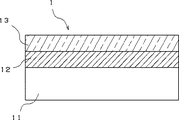
以下、本発明の実施例1を図1及び図2を参照しながら説明する。図1は、本発明の実施例1におけるバリアフィルムの構成を説明する模式図である。図2は、本発明の実施例1における光変換部材の構成を説明する模式図である。
バリアフィルム1は、図1に示す通り基材11、バリア層12、および密着性向上層13を有しており、密着性向上層13側に貼り付け対象が貼り付けられる(ラミネートされる)。また、バリア層12により外部からの水分や酸素の浸入が防止され、密着性向上層13によりバリアフィルム1と貼り付け対象との間で剥がれが生じにくくなっている。
As shown in FIG. 1, the
基材11は、透明なフィルム状の部材であり、その厚さは本実施例では約100umである。基材11の材料は特に限定はないが、たとえばPETなどの樹脂フィルムが好適に用いられる。 The base material 11 is a transparent film-like member, and its thickness is about 100 μm in this embodiment. Although the material of the base material 11 is not particularly limited, for example, a resin film such as PET is preferably used.
バリア層12は、基材11の一方の面に形成される、無機物からなる薄膜であり、二酸化ケイ素(SiO2)を成分とし、外部からの水分や酸素を透過しない性質を有する。また、二酸化ケイ素からなるバリア層12は透明な性質も有しており、基材11側から照射された光を遮蔽することなく貼り付け対象側へ透過する。
The
このバリア層12は、本説明ではプラズマCVD(Chemical Vapor Deposition)法により基材11上に形成される(成膜される)。
In this description, the
プラズマCVD法を実施するためのプラズマCVD装置は、成膜チャンバ、成膜チャンバ内に配置されたプラズマ電極、成膜チャンバ内にプラズマ形成ガスおよび原料ガスを供給する手段を有している。成膜チャンバ内にプラズマ形成ガスおよび原料ガスが供給された状態で、高周波電源によってプラズマ電極に高周波電圧が印加されることにより、プラズマ電極の周辺にプラズマが発生する。このプラズマによって原料ガスが励起されて成膜チャンバ内がプラズマ雰囲気となり、成膜チャンバ内に支持された成膜対象(本説明では基材11)の表面に所定の薄膜が形成される。 A plasma CVD apparatus for performing a plasma CVD method includes a film formation chamber, a plasma electrode disposed in the film formation chamber, and means for supplying a plasma forming gas and a source gas into the film formation chamber. A plasma is generated around the plasma electrode by applying a high frequency voltage to the plasma electrode by a high frequency power source in a state where the plasma forming gas and the source gas are supplied into the film forming chamber. The source gas is excited by this plasma, the inside of the film forming chamber becomes a plasma atmosphere, and a predetermined thin film is formed on the surface of the film forming target (the base material 11 in this description) supported in the film forming chamber.
ここで、たとえば原料ガスとしてHMDS(ヘキサメチルジシラザン)ガス、プラズマ形成ガスとして酸素ガスが供給された状態でプラズマCVD法が実施されることにより、基材11上に二酸化ケイ素が主成分であるシリコン酸化膜であるバリア層12が形成される。このようにプラズマCVD法によって形成されるバリア層12の厚みは200nm程度であり、図1では作図の都合上バリア層12も厚く見えるように図示しているが、バリア層12の厚みは基材11および後述の樹脂密着層31、光変換層100の厚みと比べて充分に薄い。
Here, for example, the plasma CVD method is performed in a state where HMDS (hexamethyldisilazane) gas as the source gas and oxygen gas as the plasma forming gas are supplied, so that silicon dioxide is the main component on the substrate 11. A
密着性向上層13は、バリア層12上に形成される薄膜であり、バリア層12と同様に透明な性質を有しており、基材11側から照射された光を遮蔽することなく貼り付け対象側へ透過する。
The
密着性向上層13は、本説明ではバリア層12と同様にプラズマCVD法によって形成され、厚みはバリア層12の厚み(約200nm)と同等である。
In this description, the
ここで、密着性向上層13はラジカル反応可能な炭化ケイ素系化合物を成分としている。ラジカル反応とは、熱や光などの形で分子にエネルギーが加えられることが起点となって、不対電子を有するラジカルがまず発生し、そのラジカルに1電子を奪われた分子が他の分子から電子を引き抜くことによりその分子がさらにラジカルを形成することである。
Here, the
特に、炭素−炭素二重結合(不飽和結合)を有する化合物ではラジカル反応が活性に作用する。ラジカル反応が生じた際、炭素−炭素二重結合は解裂し、その解裂した炭素−炭素二重結合がたとえば硬化重合段階の樹脂と反応することによって、この化合物と樹脂との間に比較的強い結合力が与えられる。 In particular, a radical reaction acts on a compound having a carbon-carbon double bond (unsaturated bond). When a radical reaction occurs, the carbon-carbon double bond is cleaved, and the cleaved carbon-carbon double bond reacts with, for example, the resin in the curing polymerization stage, thereby comparing the compound with the resin. A strong binding force is given.
本実施例では、プラズマCVD法において原料ガスにたとえばトリメトキシビニルシラン、テトラビニルシラン、1,3−ジビニルテトラメチルジシロキサン、もしくは1,1,3,3−テトラビニルジメチルジシロキサンといった炭素−炭素二重結合を有するガスが用いられることにより、炭素−炭素二重結合を含む炭化ケイ素系化合物(ラジカル反応可能な炭化ケイ素系化合物)を成分とする密着性向上層13が成膜対象(本説明ではバリア層12が形成された基材11)に形成される。なお、この際、プラズマ形成ガスとしてアルゴンなどの不活性ガスもしくはバリア層12の成膜時と比較して少量の酸素ガスが用いられる。
In this embodiment, a carbon-carbon double material such as trimethoxyvinylsilane, tetravinylsilane, 1,3-divinyltetramethyldisiloxane, or 1,1,3,3-tetravinyldimethyldisiloxane is used as a source gas in the plasma CVD method. By using a gas having a bond, the
また、HMDSガスやHMDSOガスは炭素−炭素二重結合を含んでいないが、このようなガスを原料ガスとして用いる場合であっても、たとえばエチレンもしくはアセチレンのような不飽和炭化水素ガスをプラズマ形成ガスとして用いることにより、このプラズマ形成ガスも薄膜の形成に寄与し、炭素−炭素二重結合を含む炭化ケイ素系化合物(ラジカル反応可能な炭化ケイ素系化合物)を成分とする密着性向上層13を形成することが可能である。また、少量ではあるが、不飽和炭化水素ガスをプラズマ形成ガスとして用いなくともHMDSガスやHMDSOガスがプラズマで分解される際に炭素−炭素二重結合を形成する。これを利用し、密着性向上層13を形成しても良い。
Moreover, although HMDS gas and HMSO gas do not contain a carbon-carbon double bond, even if such a gas is used as a raw material gas, an unsaturated hydrocarbon gas such as ethylene or acetylene is formed into a plasma. When used as a gas, this plasma forming gas also contributes to the formation of a thin film, and the
このように形成された密着性向上層13に貼り付け対象が貼り付けられた状態で、たとえば紫外線が照射されることにより、ラジカル反応が開始する。そして、密着性向上層13と貼り付け対象との界面でラジカル反応が連鎖することにより、密着性向上層13と貼り付け対象との結合力が向上する。
A radical reaction is started by, for example, irradiating with ultraviolet rays in a state where an object to be attached is attached to the
一方、二酸化ケイ素を主成分とするバリア層12には、炭素−炭素二重結合はほとんど存在しないため、ラジカル反応性は小さい。
On the other hand, since the
次に、実施例1にかかるバリアフィルム1が光変換層100に貼り付けられることによって形成された光変換部材10を図2に示す。
Next, the
光変換層100は、封止層101、量子ドット102、および量子ドット103を有している。
The
封止層101は、たとえば紫外線硬化性を有する樹脂であり、その厚さは本実施例では約100umである。封止層101は、量子ドット102および量子ドット103を封止し、光変換層100を形成させている。また、封止層101は透明であり、入射された光を透過する。また、封止層101は、たとえば炭素−炭素二重結合を含む炭化ケイ素系化合物といったラジカル反応可能な化合物を含有していることが好ましい。
The
また、封止層101は紫外線硬化性を有し、紫外線の照射によって重合が進行して硬化する。また、封止層101には、アゾ化合物もしくは過酸化物などラジカル反応の開始反応を生じさせるための開始剤が含まれている。
In addition, the
量子ドット102は、600nm〜680nmの範囲の波長帯域に発光中心波長を有する直径約5.0nm〜8.0nmの粒状体であり、励起光を赤色光に変換する。また、量子ドット103は、500nm〜600nmの範囲の波長帯域に発光中心波長を有する直径約1.0nm〜4.0nmの粒状体であり、励起光を緑色光に変換する。
The
この量子ドット102および量子ドット103を有する光変換層100の一方の面に励起光として青色光が入射されると、量子ドット102によって変換された赤色光、量子ドット103によって変換された緑色光、および2種の量子ドットに変換されずそのまま封止層101を通過した青色光が光変換層100の反対側の面から出射する。すなわち、光変換層100に青色光を入射させると白色光を出射させることが可能であり、このようにして得られる白色光の赤色光、緑色光、青色光の波長のピークは非常に鋭いものとなる。
When blue light is incident as excitation light on one surface of the
この光変換層100は、紫外線が照射されることにより硬化し、最終製品に利用される。ここで、本実施例では図2に示す通り、密着性向上層13が光変換層100と接するようにバリアフィルム1が光変換層100の両面に貼り付けられて光変換部材10が構成される。これによって、バリアフィルム1の外側からの水分や酸素の光変換層100への浸入をバリアフィルム1のバリア層12が阻止する。
The
そして、本実施例では図2に示す通り、バリアフィルム1の密着性向上層13に液状の光変換層100が塗布され、また、バリアフィルム1で光変換層100を挟むようにもう1枚のバリアフィルム1が貼り付けられた状態において、紫外線UVが照射されることによって、光変換層100が硬化して光変換部材10が完成する。このとき、少なくとも密着性向上層13にラジカル反応可能な化合物が含まれていることにより、紫外線UVの照射によって光変換層100の硬化が進行すると同時に密着性向上層13の連鎖的なラジカル反応が生じ、光変換層100と密着性向上層13の界面において密着性向上層13の炭素−炭素二重結合は電子を引き抜かれて解裂する。そして、解裂された炭素−炭素二重結合は硬化重合段階の光変換層100と反応し、結合するため、密着性向上層13と光変換層100との結合力が向上する。その結果、光変換層100と密着性向上層13との間での剥がれの可能性が少ない光変換部材10を得ることができる。
In this embodiment, as shown in FIG. 2, the liquid
本発明の実施例2を図3を参照しながら説明する。 A second embodiment of the present invention will be described with reference to FIG.
図3は、実施例2におけるバリアフィルム2の構成を説明する模式図である。ここで、先の実施例と同じ構成要素に関しては、先の実施例と同じ符号を用い、説明を省略する。具体的には、基材11およびバリア層12は先の実施例1と同じであり、ここでは説明を省略する。
FIG. 3 is a schematic diagram illustrating the configuration of the
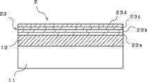
本実施例では、バリアフィルム2は密着性向上層23を有しており、これが実施例1と異なる点である。密着性向上層23の役割は、実施例1の密着性向上層13と同じく、貼り付け対象との密着性を向上させるものであるが、密着性向上層23は密着性向上層23a、密着性向上層23b、密着性向上層23c、および密着性向上層23dと複数層の構造となっている。
In this embodiment, the
これら密着性向上層23a乃至23dは、炭素−炭素二重結合を含む炭化ケイ素系化合物および二酸化ケイ素の含有量に差があり、炭素−炭素二重結合を含む炭化ケイ素系化合物の含有量は、バリア層12から遠いほど多く、二酸化ケイ素の量は、バリア層12に近いほど多くなるよう、段階的に変化している。すなわち、炭素−炭素二重結合を含む炭化ケイ素系化合物の含有量は、密着性向上層23a<密着性向上層23b<密着性向上層23c<密着性向上層23dとなっており、これとは逆に二酸化ケイ素の含有量は、密着性向上層23a>密着性向上層23b>密着性向上層23c>密着性向上層23dとなっている。
These adhesion improving layers 23a to 23d are different in the content of the silicon carbide compound containing a carbon-carbon double bond and the content of silicon dioxide, and the content of the silicon carbide compound containing a carbon-carbon double bond is The distance from the
このような炭素−炭素二重結合を含む炭化ケイ素系化合物および二酸化ケイ素の含有量に差がある複数層の密着性向上層23をプラズマCVD法によって形成する方法として、たとえばプラズマ形成ガスとして用いる酸素の供給量を変更すると良い。具体的には、密着性向上層23aの形成時は多くし、密着性向上層23dの形成時は少なくすることにより、プラズマ形成だけでなく膜の形成にも寄与する酸素の量が密着性向上層23aの形成時は多く、密着性向上層23dの形成時は少なくなるため、膜中に含有される二酸化ケイ素の分量が密着性向上層23aでは多く、密着性向上層23dでは少なくなる。そして、膜中の二酸化ケイ素の分量が多くなるにしたがい、その分炭素−炭素二重結合を含む炭化ケイ素系化合物の分量は少なくなる。
As a method for forming such a plurality of
また、プラズマ形成ガスにエチレンもしくはアセチレンといった不飽和炭化水素ガスが加えられている場合は、この不飽和炭化水素ガスの供給量を変更し、密着性向上層23aの形成時は少なくし、密着性向上層23dの形成時は多くするようにしても良い。このような方法でも、炭素−炭素二重結合を含む炭化ケイ素系化合物の含有量は、バリア層12から遠いほど多く、二酸化ケイ素の量は、バリア層12に近いほど多くすることができる。
Further, when an unsaturated hydrocarbon gas such as ethylene or acetylene is added to the plasma forming gas, the supply amount of the unsaturated hydrocarbon gas is changed so that the adhesion improving layer 23a is reduced to reduce the adhesion. You may make it increase at the time of formation of the improvement layer 23d. Even in such a method, the content of the silicon carbide-based compound including a carbon-carbon double bond can be increased as the distance from the
また、成膜の際にプラズマ電極へ印加する高周波電圧の強さを各層の形成時に変化させても良い。 Further, the strength of the high-frequency voltage applied to the plasma electrode during film formation may be changed when each layer is formed.
このように炭素−炭素二重結合を含む炭化ケイ素系化合物の含有量がバリア層12から遠いほど多く、二酸化ケイ素の量がバリア層12に近いほど多くなることにより、貼り付け対象と接する層である密着性向上層23dでは炭素−炭素二重結合を含む炭化ケイ素系化合物の含有量が多いことからラジカル反応が生じることにより充分な密着性を生じさせることができると同時に、バリア層12と接する層である密着性向上層23aは多量の二酸化ケイ素を含むことからバリア層12と組成が近似するため密着性向上層23aバリア層12との親和性が強くなる。その結果、密着性向上層23と貼り付け対象との間で剥がれが生じにくくなるだけでなく、密着性向上層23とバリア層12との間でも剥がれが生じにくくなる。
In this way, the content of the silicon carbide compound containing a carbon-carbon double bond increases as the distance from the
以下、本発明の実施例3を図4及び図5を参照しながら説明する。図4は、本発明の実施例3におけるバリアフィルムの構成を説明する模式図である。図5は、本発明の実施例3における光変換部材の構成を説明する模式図である。 A third embodiment of the present invention will be described below with reference to FIGS. FIG. 4 is a schematic diagram illustrating the configuration of the barrier film in Example 3 of the present invention. FIG. 5 is a schematic diagram illustrating the configuration of the light conversion member according to the third embodiment of the present invention.
ここで、先の実施例と同じ構成要素に関しては、先の実施例と同じ符号を用い、説明を省略する。具体的には、基材11、バリア層12、密着性向上層13は先の実施例1と同じであり、ここでは説明を省略する。
Here, with respect to the same components as in the previous embodiment, the same reference numerals as in the previous embodiment are used, and description thereof is omitted. Specifically, the base material 11, the
実施例3におけるバリアフィルム3は、図4に示す通り、密着性向上層13上にさらに樹脂密着層31が設けられている。樹脂密着層31は、紫外線硬化性を有する樹脂から構成される層であり、その厚さは本実施例では約100umである。本実施例では、この樹脂密着層31が貼り付け対象と接し、貼り付けられる。また、樹脂密着層31には、アゾ化合物もしくは過酸化物などラジカル反応の開始反応を生じさせるための開始剤が含まれている。
As shown in FIG. 4, the barrier film 3 in Example 3 is further provided with a
ここで、樹脂密着層31と密着性向上層13、および樹脂密着層31と貼り付け対象との密着性を高めるために、炭素−炭素二重結合を含む炭化ケイ素系化合物などラジカル反応可能な化合物が樹脂密着層31に含有されていることが好ましい。
Here, in order to improve the adhesion between the
次に、実施例3にかかるバリアフィルム3が光変換層100に貼り付けられることによって形成された光変換部材30を図5に示す。
Next, the
図5に示す通り、樹脂密着層31が光変換層100と接するように液状の光変換層100がバリアフィルム3に塗布され、また、バリアフィルム3で光変換層100を挟むようにもう1枚のバリアフィルム3が貼り付けられて光変換部材30が構成される。そして、バリアフィルム3が光変換層100に貼り付けられた後、紫外線UVが照射されることによって、樹脂密着層31および光変換層100とが同時に硬化し、また、樹脂密着層31と密着性向上層13との界面でラジカル反応が連鎖的に生じて樹脂密着層31と密着性向上層13との間の結合力が向上する。
As shown in FIG. 5, the liquid
ここで、光変換層100を構成する封止層101の材料の中には、紫外線照射によって硬化する際に大きな収縮率で収縮するものもある。これに対し、密着性向上層13の紫外線照射による収縮はほとんど無いが、本実施例の通り光変換層100と密着性向上層13との間に樹脂密着層31が介在するため、硬化前は図5の2点鎖線で示した通りの大きさであった光変換層100が収縮した際に、この光変換層100との接触状態を維持するように樹脂密着層31が変形する。これによって、光変換層100が収縮した後も光変換層100と樹脂密着層31との間で両者を引き剥がす程度の応力は生じず、また、樹脂密着層31と密着性向上層13との間でも両者を引き剥がす程度の応力は生じない。そのため、剥がれを生じさせずに光変換部材30を得ることができる。
Here, some of the material of the
一方、仮に上記の通り大きな収縮率を有する光変換層100に対し、図2のように密着性向上層13が直接貼り付けて紫外線UVの照射が行われた場合、両者の間で連鎖的なラジカル反応が生じるものの両者の収縮率の差および弾性係数の差に起因する応力が両者の界面で生じ、両者を引き剥がすように働く。この応力が連鎖的なラジカル反応によって向上した密着力よりも大きい場合、光変換層100と密着性向上層13との間で剥がれが生じる可能性がある。
On the other hand, if the
以上の通り、大きな収縮率を有する光変換層100が用いられる場合、本実施例の通り樹脂密着層31が有効に作用する。また、このように紫外線照射時に光変換層100の収縮に合わせて変形させるために、樹脂密着層31の材料として、特に伸び(伸度)が200%以上であるウレタンアクリレート系の樹脂が好適に用いられる。また、伸びが300%以上だとなお良い。
As described above, when the
次に、上記の実施例3にかかる光変換部材30の密着力と従来技術による光変換部材の密着力との比較結果を以下に示す。
Next, a comparison result between the adhesion force of the
実施例3にかかる光変換部材30は、図5に示す通り、基材11上にバリア層12、密着性向上層13、および樹脂密着層31が形成されたバリアフィルム3を光変換層100に貼り付けて硬化させたものである。これに対し、比較例(従来技術の一例)として、図6に示すように基材11上にバリア層12および樹脂密着層31が形成されたバリアフィルムを光変換層100に貼り付けて硬化させた光変換部材90を準備した。すなわち、実施例3と比較して密着性向上層13が形成されていない点が異なる。
As illustrated in FIG. 5, the
これら光変換部材30と光変換部材90のサンプルに対し、それぞれのバリアフィルムを光変換層100との接着面と垂直な方向に20mm/minの速度で剥離させた際の密着力の最小値をそれぞれ複数回ずつ測定した。
For the samples of the
その結果、光変換部材90にかかるサンプルでは密着力の最小値が0〜0.5N/25mmであったのに対し、光変換部材30にかかるサンプルでは密着力の最小値が8〜10N/25mmとなり、密着性向上層13が存在することによる顕著な密着力の強化を確認することができた。
As a result, in the sample applied to the
以上のバリアフィルムおよび光変換部材により、剥がれを生じさせずに外部からの水分や酸素の浸入を防止することが可能である。 With the above barrier film and light conversion member, it is possible to prevent moisture and oxygen from entering from the outside without causing peeling.
ここで、本発明のバリアフィルムおよび光変換部材は、以上で説明した形態に限らず本発明の範囲内において他の形態のものであってもよい。たとえば、上記の説明ではバリア層および密着性向上層はプラズマCVD法により形成しているが、必ずしもこれに限定されず、他の手段によってバリア層および密着性向上層を形成してもよい。具体的には、スパッタリング、真空蒸着法などを用いて形成しても良い。 Here, the barrier film and the light conversion member of the present invention are not limited to the forms described above, and may be in other forms within the scope of the present invention. For example, in the above description, the barrier layer and the adhesion improving layer are formed by the plasma CVD method. However, the present invention is not necessarily limited thereto, and the barrier layer and the adhesion improving layer may be formed by other means. Specifically, it may be formed using sputtering, vacuum deposition, or the like.
また、上記の実施例2ではバリア層12と接する密着性向上層23aが二酸化ケイ素を多く含むようにし、両者の密着力を高めているが、そもそもバリア層と密着性向上層とはともにプラズマCVD法により、同じ原料ガスもしくは同系の有機ケイ素モノマーから形成されるものであるため、密着性は比較的高い。そのため、バリア層と密着性向上層との間で剥がれを心配する必要が無い場合は、実施例1や実施例3のように二酸化ケイ素の含有量が少ない単層の密着性向上層であっても良い。
In Example 2 described above, the adhesion improving layer 23a in contact with the
1 バリアフィルム
2 バリアフィルム
3 バリアフィルム
10 光変換部材
11 基材
12 バリア層
13 密着性向上層
23 密着性向上層
23a 密着性向上層
23b 密着性向上層
23c 密着性向上層
23d 密着性向上層
30 光変換部材
31 樹脂密着層
90 光変換部材
100 光変換層
101 封止層
102 量子ドット
103 量子ドット
UV 紫外線
DESCRIPTION OF
Claims (5)
前記基材の一方の面上に形成された、二酸化ケイ素を主成分とする薄膜状のバリア層と、
前記バリア層上に形成された、炭素−炭素二重結合を含む炭化ケイ素系化合物を成分とする薄膜状の密着性向上層と、
を有することを特徴とする、バリアフィルム。 A transparent film substrate;
A thin-film barrier layer mainly composed of silicon dioxide formed on one surface of the substrate;
A thin film-like adhesion improving layer comprising a silicon carbide compound containing a carbon-carbon double bond formed on the barrier layer;
A barrier film characterized by comprising:
前記基材の一方の面上に形成された、二酸化ケイ素を主成分とする薄膜状のバリア層と、
前記バリア層上に形成された、炭素−炭素二重結合を含む炭化ケイ素系化合物を成分とする薄膜状の密着性向上層と、
を有するバリアフィルムの前記密着性向上層上に、紫外線硬化型の光変換層が設けられていることを特徴とする、光変換部材。 A transparent film substrate;
A thin-film barrier layer mainly composed of silicon dioxide formed on one surface of the substrate;
A thin film-like adhesion improving layer comprising a silicon carbide compound containing a carbon-carbon double bond formed on the barrier layer;
An ultraviolet conversion type light conversion layer is provided on the adhesion improving layer of the barrier film having a light conversion member.
前記基材の一方の面上に形成された、二酸化ケイ素を主成分とする薄膜状のバリア層と、
前記バリア層上に形成された、炭素−炭素二重結合を含む炭化ケイ素系化合物を成分とする薄膜状の密着性向上層と、
前記密着性向上層上に設けられた、紫外線硬化型の樹脂からなる樹脂密着層と、
を有するバリアフィルムの前記樹脂密着層上に、紫外線硬化型の光変換層が設けられていることを特徴とする、光変換部材。 A transparent film substrate;
A thin-film barrier layer mainly composed of silicon dioxide formed on one surface of the substrate;
A thin film-like adhesion improving layer comprising a silicon carbide compound containing a carbon-carbon double bond formed on the barrier layer;
A resin adhesion layer made of an ultraviolet curable resin provided on the adhesion improvement layer;
An ultraviolet conversion type light conversion layer is provided on the resin adhesion layer of a barrier film having a light conversion member.
Priority Applications (2)
| Application Number | Priority Date | Filing Date | Title |
|---|---|---|---|
| JP2018045020A JP7163041B2 (en) | 2018-03-13 | 2018-03-13 | Barrier film and light conversion material |
| PCT/JP2019/009987 WO2019176936A1 (en) | 2018-03-13 | 2019-03-12 | Barrier film and light conversion member |
Applications Claiming Priority (1)
| Application Number | Priority Date | Filing Date | Title |
|---|---|---|---|
| JP2018045020A JP7163041B2 (en) | 2018-03-13 | 2018-03-13 | Barrier film and light conversion material |
Publications (2)
| Publication Number | Publication Date |
|---|---|
| JP2019155704A true JP2019155704A (en) | 2019-09-19 |
| JP7163041B2 JP7163041B2 (en) | 2022-10-31 |
Family
ID=67906771
Family Applications (1)
| Application Number | Title | Priority Date | Filing Date |
|---|---|---|---|
| JP2018045020A Active JP7163041B2 (en) | 2018-03-13 | 2018-03-13 | Barrier film and light conversion material |
Country Status (2)
| Country | Link |
|---|---|
| JP (1) | JP7163041B2 (en) |
| WO (1) | WO2019176936A1 (en) |
Citations (12)
| Publication number | Priority date | Publication date | Assignee | Title |
|---|---|---|---|---|
| JP2002200455A (en) * | 2000-12-28 | 2002-07-16 | Chugoku Marine Paints Ltd | Composite body, base material coated with coating film composed of the composite body and method of manufacturing base material with coating film |
| JP2008069407A (en) * | 2006-09-14 | 2008-03-27 | Toyo Seikan Kaisha Ltd | Method for producing polylactic acid molding |
| JP2008254794A (en) * | 2007-04-06 | 2008-10-23 | Toyo Seikan Kaisha Ltd | Plastic molded product with vapor deposition film and its manufacturing method |
| WO2012091097A1 (en) * | 2010-12-28 | 2012-07-05 | 麒麟麦酒株式会社 | Gas-barrier plastic molded product and manufacturing process therefor |
| JP2013043383A (en) * | 2011-08-24 | 2013-03-04 | Fujifilm Corp | Barrier laminate, gas barrier film, and device using barrier laminate or gas barrier film |
| WO2016059843A1 (en) * | 2014-10-16 | 2016-04-21 | 凸版印刷株式会社 | Quantum dot protective film, quantum dot film using same, and backlight unit |
| JP2016068556A (en) * | 2014-09-26 | 2016-05-09 | 富士フイルム株式会社 | Laminate film, backlight unit, liquid crystal display device, and production method of laminate film |
| WO2016104401A1 (en) * | 2014-12-26 | 2016-06-30 | Nsマテリアルズ株式会社 | Wavelength conversion member and method for manufacturing same |
| JP2016141744A (en) * | 2015-02-02 | 2016-08-08 | 富士フイルム株式会社 | Composition for wavelength conversion layer, wavelength conversion member, backlight unit, and liquid crystal display device |
| WO2016167152A1 (en) * | 2015-04-17 | 2016-10-20 | キリン株式会社 | Gas-barrier plastic molded product and method for manufacturing same |
| JP2017016134A (en) * | 2013-09-13 | 2017-01-19 | 凸版印刷株式会社 | Wavelength conversion sheet and backlight unit |
| JP2017177668A (en) * | 2016-03-31 | 2017-10-05 | 凸版印刷株式会社 | Barrier film and method for producing the same, and wavelength conversion sheet and method for producing the same |
-
2018
- 2018-03-13 JP JP2018045020A patent/JP7163041B2/en active Active
-
2019
- 2019-03-12 WO PCT/JP2019/009987 patent/WO2019176936A1/en active Application Filing
Patent Citations (12)
| Publication number | Priority date | Publication date | Assignee | Title |
|---|---|---|---|---|
| JP2002200455A (en) * | 2000-12-28 | 2002-07-16 | Chugoku Marine Paints Ltd | Composite body, base material coated with coating film composed of the composite body and method of manufacturing base material with coating film |
| JP2008069407A (en) * | 2006-09-14 | 2008-03-27 | Toyo Seikan Kaisha Ltd | Method for producing polylactic acid molding |
| JP2008254794A (en) * | 2007-04-06 | 2008-10-23 | Toyo Seikan Kaisha Ltd | Plastic molded product with vapor deposition film and its manufacturing method |
| WO2012091097A1 (en) * | 2010-12-28 | 2012-07-05 | 麒麟麦酒株式会社 | Gas-barrier plastic molded product and manufacturing process therefor |
| JP2013043383A (en) * | 2011-08-24 | 2013-03-04 | Fujifilm Corp | Barrier laminate, gas barrier film, and device using barrier laminate or gas barrier film |
| JP2017016134A (en) * | 2013-09-13 | 2017-01-19 | 凸版印刷株式会社 | Wavelength conversion sheet and backlight unit |
| JP2016068556A (en) * | 2014-09-26 | 2016-05-09 | 富士フイルム株式会社 | Laminate film, backlight unit, liquid crystal display device, and production method of laminate film |
| WO2016059843A1 (en) * | 2014-10-16 | 2016-04-21 | 凸版印刷株式会社 | Quantum dot protective film, quantum dot film using same, and backlight unit |
| WO2016104401A1 (en) * | 2014-12-26 | 2016-06-30 | Nsマテリアルズ株式会社 | Wavelength conversion member and method for manufacturing same |
| JP2016141744A (en) * | 2015-02-02 | 2016-08-08 | 富士フイルム株式会社 | Composition for wavelength conversion layer, wavelength conversion member, backlight unit, and liquid crystal display device |
| WO2016167152A1 (en) * | 2015-04-17 | 2016-10-20 | キリン株式会社 | Gas-barrier plastic molded product and method for manufacturing same |
| JP2017177668A (en) * | 2016-03-31 | 2017-10-05 | 凸版印刷株式会社 | Barrier film and method for producing the same, and wavelength conversion sheet and method for producing the same |
Also Published As
| Publication number | Publication date |
|---|---|
| WO2019176936A1 (en) | 2019-09-19 |
| JP7163041B2 (en) | 2022-10-31 |
Similar Documents
| Publication | Publication Date | Title |
|---|---|---|
| WO2018214257A1 (en) | Packaging thin film and manufacturing method therefor, and packaging method for oled panel | |
| JP5469059B2 (en) | Organic electronic devices protected by elastic laminate adhesives | |
| JP6309787B2 (en) | Organic EL laminate | |
| JP6814157B2 (en) | Adhesive composition, encapsulation sheet, and encapsulant | |
| JP5914397B2 (en) | Functional film | |
| JP2013047007A (en) | Transparent laminate | |
| CN109964155A (en) | Containing fluorescent membrane and back light unit | |
| JP6600013B2 (en) | Wavelength conversion film | |
| JP2016182744A (en) | Functional film and method for producing functional film | |
| JP7158377B2 (en) | Gas barrier film and sealant | |
| KR20210024151A (en) | Barrier film, wavelength conversion sheet, and manufacturing method of wavelength conversion sheet | |
| JP6170627B2 (en) | Electronic device manufacturing method and composite film | |
| TW201815561A (en) | Gas barrier laminate and sealed body | |
| JP2017043058A (en) | Production method of gas barrier film and transfer method of gas barrier film | |
| JPWO2010024149A1 (en) | Composite film, gas barrier film, method for producing the same, and organic electroluminescence device | |
| JP4419012B2 (en) | Organic EL element sealing material and organic EL element sealing method | |
| JP2016204461A (en) | Functional film and manufacturing method of functional film | |
| WO2019176936A1 (en) | Barrier film and light conversion member | |
| JP6262108B2 (en) | Method for producing functional film | |
| JP6744487B2 (en) | Gas barrier film and method for producing gas barrier film | |
| JP2005011649A (en) | Bonding method, manufacturing method of electroluminescent panel capable of utilizing the bonding method, and electroluminescent panel | |
| JP6720473B2 (en) | Light emitting device, lighting fixture, information display device, and method for manufacturing light emitting device | |
| JP2017134254A (en) | Protective film for wavelength conversion sheet | |
| JPWO2020066496A1 (en) | Manufacturing method of electronic device laminate and electronic device laminate | |
| JP7188669B2 (en) | Encapsulation manufacturing method |
Legal Events
| Date | Code | Title | Description |
|---|---|---|---|
| A621 | Written request for application examination |
Free format text: JAPANESE INTERMEDIATE CODE: A621 Effective date: 20201126 |
|
| A131 | Notification of reasons for refusal |
Free format text: JAPANESE INTERMEDIATE CODE: A131 Effective date: 20211006 |
|
| A521 | Request for written amendment filed |
Free format text: JAPANESE INTERMEDIATE CODE: A523 Effective date: 20211126 |
|
| A131 | Notification of reasons for refusal |
Free format text: JAPANESE INTERMEDIATE CODE: A131 Effective date: 20220323 |
|
| A521 | Request for written amendment filed |
Free format text: JAPANESE INTERMEDIATE CODE: A523 Effective date: 20220519 |
|
| TRDD | Decision of grant or rejection written | ||
| A01 | Written decision to grant a patent or to grant a registration (utility model) |
Free format text: JAPANESE INTERMEDIATE CODE: A01 Effective date: 20221004 |
|
| A61 | First payment of annual fees (during grant procedure) |
Free format text: JAPANESE INTERMEDIATE CODE: A61 Effective date: 20221019 |
|
| R150 | Certificate of patent or registration of utility model |
Ref document number: 7163041 Country of ref document: JP Free format text: JAPANESE INTERMEDIATE CODE: R150 |