JP2019117797A - Light-emitting device - Google Patents
Light-emitting device Download PDFInfo
- Publication number
- JP2019117797A JP2019117797A JP2019035436A JP2019035436A JP2019117797A JP 2019117797 A JP2019117797 A JP 2019117797A JP 2019035436 A JP2019035436 A JP 2019035436A JP 2019035436 A JP2019035436 A JP 2019035436A JP 2019117797 A JP2019117797 A JP 2019117797A
- Authority
- JP
- Japan
- Prior art keywords
- layer
- electrode
- substrate
- light
- light emitting
- Prior art date
- Legal status (The legal status is an assumption and is not a legal conclusion. Google has not performed a legal analysis and makes no representation as to the accuracy of the status listed.)
- Granted
Links
- 239000000758 substrate Substances 0.000 claims abstract description 257
- 238000005192 partition Methods 0.000 claims description 55
- 239000011347 resin Substances 0.000 claims description 33
- 229920005989 resin Polymers 0.000 claims description 33
- 239000002245 particle Substances 0.000 claims description 8
- 239000010410 layer Substances 0.000 abstract description 536
- 239000012790 adhesive layer Substances 0.000 abstract description 89
- 230000015572 biosynthetic process Effects 0.000 abstract description 69
- 238000004519 manufacturing process Methods 0.000 abstract description 50
- 238000012546 transfer Methods 0.000 abstract description 20
- 238000000034 method Methods 0.000 description 133
- 238000005401 electroluminescence Methods 0.000 description 87
- 239000000463 material Substances 0.000 description 83
- 239000002585 base Substances 0.000 description 49
- 239000004065 semiconductor Substances 0.000 description 43
- 229910052751 metal Inorganic materials 0.000 description 30
- 239000002184 metal Substances 0.000 description 29
- 230000006870 function Effects 0.000 description 28
- 239000004973 liquid crystal related substance Substances 0.000 description 28
- 239000010408 film Substances 0.000 description 27
- 230000002093 peripheral effect Effects 0.000 description 22
- 239000000126 substance Substances 0.000 description 18
- WFKWXMTUELFFGS-UHFFFAOYSA-N tungsten Chemical compound [W] WFKWXMTUELFFGS-UHFFFAOYSA-N 0.000 description 18
- 229910052721 tungsten Inorganic materials 0.000 description 18
- 239000010937 tungsten Substances 0.000 description 18
- 229910052782 aluminium Inorganic materials 0.000 description 13
- XAGFODPZIPBFFR-UHFFFAOYSA-N aluminium Chemical compound [Al] XAGFODPZIPBFFR-UHFFFAOYSA-N 0.000 description 13
- 230000002829 reductive effect Effects 0.000 description 12
- 238000004544 sputter deposition Methods 0.000 description 12
- 230000009977 dual effect Effects 0.000 description 11
- 239000012535 impurity Substances 0.000 description 11
- QVGXLLKOCUKJST-UHFFFAOYSA-N atomic oxygen Chemical compound [O] QVGXLLKOCUKJST-UHFFFAOYSA-N 0.000 description 10
- 239000004020 conductor Substances 0.000 description 10
- 150000002894 organic compounds Chemical class 0.000 description 10
- 239000001301 oxygen Substances 0.000 description 10
- 229910052760 oxygen Inorganic materials 0.000 description 10
- 238000000926 separation method Methods 0.000 description 10
- VYPSYNLAJGMNEJ-UHFFFAOYSA-N silicon dioxide Inorganic materials O=[Si]=O VYPSYNLAJGMNEJ-UHFFFAOYSA-N 0.000 description 10
- 239000000243 solution Substances 0.000 description 10
- ZOKXTWBITQBERF-UHFFFAOYSA-N Molybdenum Chemical compound [Mo] ZOKXTWBITQBERF-UHFFFAOYSA-N 0.000 description 9
- 238000009792 diffusion process Methods 0.000 description 9
- 238000005530 etching Methods 0.000 description 9
- AMGQUBHHOARCQH-UHFFFAOYSA-N indium;oxotin Chemical compound [In].[Sn]=O AMGQUBHHOARCQH-UHFFFAOYSA-N 0.000 description 9
- 229910052750 molybdenum Inorganic materials 0.000 description 9
- 239000011733 molybdenum Substances 0.000 description 9
- NBIIXXVUZAFLBC-UHFFFAOYSA-N Phosphoric acid Chemical compound OP(O)(O)=O NBIIXXVUZAFLBC-UHFFFAOYSA-N 0.000 description 8
- RTAQQCXQSZGOHL-UHFFFAOYSA-N Titanium Chemical compound [Ti] RTAQQCXQSZGOHL-UHFFFAOYSA-N 0.000 description 8
- 239000000956 alloy Substances 0.000 description 8
- 238000000576 coating method Methods 0.000 description 8
- 239000011521 glass Substances 0.000 description 8
- 229910044991 metal oxide Inorganic materials 0.000 description 8
- 150000004706 metal oxides Chemical class 0.000 description 8
- 239000011368 organic material Substances 0.000 description 8
- 238000005498 polishing Methods 0.000 description 8
- 239000002356 single layer Substances 0.000 description 8
- 229910052719 titanium Inorganic materials 0.000 description 8
- 239000010936 titanium Substances 0.000 description 8
- 239000004925 Acrylic resin Substances 0.000 description 7
- 229920000178 Acrylic resin Polymers 0.000 description 7
- 150000001875 compounds Chemical class 0.000 description 7
- 229910052814 silicon oxide Inorganic materials 0.000 description 7
- QTBSBXVTEAMEQO-UHFFFAOYSA-N Acetic acid Chemical compound CC(O)=O QTBSBXVTEAMEQO-UHFFFAOYSA-N 0.000 description 6
- MUBZPKHOEPUJKR-UHFFFAOYSA-N Oxalic acid Chemical compound OC(=O)C(O)=O MUBZPKHOEPUJKR-UHFFFAOYSA-N 0.000 description 6
- XUIMIQQOPSSXEZ-UHFFFAOYSA-N Silicon Chemical compound [Si] XUIMIQQOPSSXEZ-UHFFFAOYSA-N 0.000 description 6
- 229910045601 alloy Inorganic materials 0.000 description 6
- 239000002131 composite material Substances 0.000 description 6
- 238000001312 dry etching Methods 0.000 description 6
- 239000011810 insulating material Substances 0.000 description 6
- 239000011159 matrix material Substances 0.000 description 6
- 238000007639 printing Methods 0.000 description 6
- 230000008569 process Effects 0.000 description 6
- 230000001681 protective effect Effects 0.000 description 6
- 229910052710 silicon Inorganic materials 0.000 description 6
- 239000010703 silicon Substances 0.000 description 6
- XLYOFNOQVPJJNP-UHFFFAOYSA-N water Substances O XLYOFNOQVPJJNP-UHFFFAOYSA-N 0.000 description 6
- PXHVJJICTQNCMI-UHFFFAOYSA-N Nickel Chemical compound [Ni] PXHVJJICTQNCMI-UHFFFAOYSA-N 0.000 description 5
- 229910052581 Si3N4 Inorganic materials 0.000 description 5
- GWEVSGVZZGPLCZ-UHFFFAOYSA-N Titan oxide Chemical compound O=[Ti]=O GWEVSGVZZGPLCZ-UHFFFAOYSA-N 0.000 description 5
- QCWXUUIWCKQGHC-UHFFFAOYSA-N Zirconium Chemical compound [Zr] QCWXUUIWCKQGHC-UHFFFAOYSA-N 0.000 description 5
- 239000000853 adhesive Substances 0.000 description 5
- 230000001070 adhesive effect Effects 0.000 description 5
- 238000001962 electrophoresis Methods 0.000 description 5
- 150000003949 imides Chemical class 0.000 description 5
- 230000003647 oxidation Effects 0.000 description 5
- 238000007254 oxidation reaction Methods 0.000 description 5
- 229920001721 polyimide Polymers 0.000 description 5
- 239000009719 polyimide resin Substances 0.000 description 5
- HQVNEWCFYHHQES-UHFFFAOYSA-N silicon nitride Chemical compound N12[Si]34N5[Si]62N3[Si]51N64 HQVNEWCFYHHQES-UHFFFAOYSA-N 0.000 description 5
- 229910052709 silver Inorganic materials 0.000 description 5
- 239000004332 silver Substances 0.000 description 5
- 238000001039 wet etching Methods 0.000 description 5
- 229910052726 zirconium Inorganic materials 0.000 description 5
- IJGRMHOSHXDMSA-UHFFFAOYSA-N Atomic nitrogen Chemical compound N#N IJGRMHOSHXDMSA-UHFFFAOYSA-N 0.000 description 4
- LFQSCWFLJHTTHZ-UHFFFAOYSA-N Ethanol Chemical compound CCO LFQSCWFLJHTTHZ-UHFFFAOYSA-N 0.000 description 4
- 229910000147 aluminium phosphate Inorganic materials 0.000 description 4
- 230000008859 change Effects 0.000 description 4
- 230000005684 electric field Effects 0.000 description 4
- 230000004048 modification Effects 0.000 description 4
- 238000012986 modification Methods 0.000 description 4
- QGLKJKCYBOYXKC-UHFFFAOYSA-N nonaoxidotritungsten Chemical compound O=[W]1(=O)O[W](=O)(=O)O[W](=O)(=O)O1 QGLKJKCYBOYXKC-UHFFFAOYSA-N 0.000 description 4
- 239000003960 organic solvent Substances 0.000 description 4
- -1 polyethylene terephthalate Polymers 0.000 description 4
- 238000012545 processing Methods 0.000 description 4
- 229910001930 tungsten oxide Inorganic materials 0.000 description 4
- 239000004986 Cholesteric liquid crystals (ChLC) Substances 0.000 description 3
- 206010034972 Photosensitivity reaction Diseases 0.000 description 3
- 239000004983 Polymer Dispersed Liquid Crystal Substances 0.000 description 3
- 229910021536 Zeolite Inorganic materials 0.000 description 3
- 230000009471 action Effects 0.000 description 3
- 229910052784 alkaline earth metal Inorganic materials 0.000 description 3
- 150000001342 alkaline earth metals Chemical class 0.000 description 3
- 230000003321 amplification Effects 0.000 description 3
- QVQLCTNNEUAWMS-UHFFFAOYSA-N barium oxide Chemical compound [Ba]=O QVQLCTNNEUAWMS-UHFFFAOYSA-N 0.000 description 3
- 230000005540 biological transmission Effects 0.000 description 3
- 239000003990 capacitor Substances 0.000 description 3
- 238000005229 chemical vapour deposition Methods 0.000 description 3
- 239000011651 chromium Substances 0.000 description 3
- 230000000295 complement effect Effects 0.000 description 3
- PMHQVHHXPFUNSP-UHFFFAOYSA-M copper(1+);methylsulfanylmethane;bromide Chemical compound Br[Cu].CSC PMHQVHHXPFUNSP-UHFFFAOYSA-M 0.000 description 3
- 239000013078 crystal Substances 0.000 description 3
- 239000002274 desiccant Substances 0.000 description 3
- HNPSIPDUKPIQMN-UHFFFAOYSA-N dioxosilane;oxo(oxoalumanyloxy)alumane Chemical compound O=[Si]=O.O=[Al]O[Al]=O HNPSIPDUKPIQMN-UHFFFAOYSA-N 0.000 description 3
- 239000003822 epoxy resin Substances 0.000 description 3
- 238000001704 evaporation Methods 0.000 description 3
- 238000000605 extraction Methods 0.000 description 3
- 229910003437 indium oxide Inorganic materials 0.000 description 3
- PJXISJQVUVHSOJ-UHFFFAOYSA-N indium(iii) oxide Chemical compound [O-2].[O-2].[O-2].[In+3].[In+3] PJXISJQVUVHSOJ-UHFFFAOYSA-N 0.000 description 3
- 238000002347 injection Methods 0.000 description 3
- 239000007924 injection Substances 0.000 description 3
- 238000003475 lamination Methods 0.000 description 3
- 239000002346 layers by function Substances 0.000 description 3
- 239000007769 metal material Substances 0.000 description 3
- 229910052759 nickel Inorganic materials 0.000 description 3
- 239000010955 niobium Substances 0.000 description 3
- 238000003199 nucleic acid amplification method Methods 0.000 description 3
- 230000003287 optical effect Effects 0.000 description 3
- 230000001590 oxidative effect Effects 0.000 description 3
- TWNQGVIAIRXVLR-UHFFFAOYSA-N oxo(oxoalumanyloxy)alumane Chemical compound O=[Al]O[Al]=O TWNQGVIAIRXVLR-UHFFFAOYSA-N 0.000 description 3
- 230000000149 penetrating effect Effects 0.000 description 3
- 238000000206 photolithography Methods 0.000 description 3
- 230000036211 photosensitivity Effects 0.000 description 3
- 238000005268 plasma chemical vapour deposition Methods 0.000 description 3
- 229920000647 polyepoxide Polymers 0.000 description 3
- 229920000642 polymer Polymers 0.000 description 3
- 239000010453 quartz Substances 0.000 description 3
- 238000003860 storage Methods 0.000 description 3
- 229910052715 tantalum Inorganic materials 0.000 description 3
- GUVRBAGPIYLISA-UHFFFAOYSA-N tantalum atom Chemical compound [Ta] GUVRBAGPIYLISA-UHFFFAOYSA-N 0.000 description 3
- 229920001187 thermosetting polymer Polymers 0.000 description 3
- OGIDPMRJRNCKJF-UHFFFAOYSA-N titanium oxide Inorganic materials [Ti]=O OGIDPMRJRNCKJF-UHFFFAOYSA-N 0.000 description 3
- 239000010457 zeolite Substances 0.000 description 3
- YVTHLONGBIQYBO-UHFFFAOYSA-N zinc indium(3+) oxygen(2-) Chemical compound [O--].[Zn++].[In+3] YVTHLONGBIQYBO-UHFFFAOYSA-N 0.000 description 3
- VYZAMTAEIAYCRO-UHFFFAOYSA-N Chromium Chemical compound [Cr] VYZAMTAEIAYCRO-UHFFFAOYSA-N 0.000 description 2
- 239000004988 Nematic liquid crystal Substances 0.000 description 2
- GRYLNZFGIOXLOG-UHFFFAOYSA-N Nitric acid Chemical compound O[N+]([O-])=O GRYLNZFGIOXLOG-UHFFFAOYSA-N 0.000 description 2
- CBENFWSGALASAD-UHFFFAOYSA-N Ozone Chemical compound [O-][O+]=O CBENFWSGALASAD-UHFFFAOYSA-N 0.000 description 2
- KDLHZDBZIXYQEI-UHFFFAOYSA-N Palladium Chemical compound [Pd] KDLHZDBZIXYQEI-UHFFFAOYSA-N 0.000 description 2
- NRTOMJZYCJJWKI-UHFFFAOYSA-N Titanium nitride Chemical compound [Ti]#N NRTOMJZYCJJWKI-UHFFFAOYSA-N 0.000 description 2
- XLOMVQKBTHCTTD-UHFFFAOYSA-N Zinc monoxide Chemical compound [Zn]=O XLOMVQKBTHCTTD-UHFFFAOYSA-N 0.000 description 2
- 239000002390 adhesive tape Substances 0.000 description 2
- 229910052783 alkali metal Inorganic materials 0.000 description 2
- 150000001340 alkali metals Chemical class 0.000 description 2
- 229910052804 chromium Inorganic materials 0.000 description 2
- 239000003086 colorant Substances 0.000 description 2
- 235000019441 ethanol Nutrition 0.000 description 2
- 239000005262 ferroelectric liquid crystals (FLCs) Substances 0.000 description 2
- 239000012530 fluid Substances 0.000 description 2
- 229910052737 gold Inorganic materials 0.000 description 2
- 239000010931 gold Substances 0.000 description 2
- 239000003094 microcapsule Substances 0.000 description 2
- 229910052758 niobium Inorganic materials 0.000 description 2
- GUCVJGMIXFAOAE-UHFFFAOYSA-N niobium atom Chemical compound [Nb] GUCVJGMIXFAOAE-UHFFFAOYSA-N 0.000 description 2
- 229910017604 nitric acid Inorganic materials 0.000 description 2
- 229910052757 nitrogen Inorganic materials 0.000 description 2
- 235000006408 oxalic acid Nutrition 0.000 description 2
- 239000004033 plastic Substances 0.000 description 2
- 229920003023 plastic Polymers 0.000 description 2
- BASFCYQUMIYNBI-UHFFFAOYSA-N platinum Chemical compound [Pt] BASFCYQUMIYNBI-UHFFFAOYSA-N 0.000 description 2
- 230000004044 response Effects 0.000 description 2
- 238000005476 soldering Methods 0.000 description 2
- 230000005236 sound signal Effects 0.000 description 2
- 238000004528 spin coating Methods 0.000 description 2
- 239000010409 thin film Substances 0.000 description 2
- 241001253177 Anisotes Species 0.000 description 1
- JBRZTFJDHDCESZ-UHFFFAOYSA-N AsGa Chemical compound [As]#[Ga] JBRZTFJDHDCESZ-UHFFFAOYSA-N 0.000 description 1
- RYGMFSIKBFXOCR-UHFFFAOYSA-N Copper Chemical compound [Cu] RYGMFSIKBFXOCR-UHFFFAOYSA-N 0.000 description 1
- 239000004985 Discotic Liquid Crystal Substance Substances 0.000 description 1
- 229910001218 Gallium arsenide Inorganic materials 0.000 description 1
- 239000005264 High molar mass liquid crystal Substances 0.000 description 1
- 239000004976 Lyotropic liquid crystal Substances 0.000 description 1
- FYYHWMGAXLPEAU-UHFFFAOYSA-N Magnesium Chemical compound [Mg] FYYHWMGAXLPEAU-UHFFFAOYSA-N 0.000 description 1
- 240000005561 Musa balbisiana Species 0.000 description 1
- 235000018290 Musa x paradisiaca Nutrition 0.000 description 1
- 229910052779 Neodymium Inorganic materials 0.000 description 1
- OAICVXFJPJFONN-UHFFFAOYSA-N Phosphorus Chemical compound [P] OAICVXFJPJFONN-UHFFFAOYSA-N 0.000 description 1
- 239000004962 Polyamide-imide Substances 0.000 description 1
- 239000004695 Polyether sulfone Substances 0.000 description 1
- KJTLSVCANCCWHF-UHFFFAOYSA-N Ruthenium Chemical compound [Ru] KJTLSVCANCCWHF-UHFFFAOYSA-N 0.000 description 1
- BQCADISMDOOEFD-UHFFFAOYSA-N Silver Chemical compound [Ag] BQCADISMDOOEFD-UHFFFAOYSA-N 0.000 description 1
- 239000004990 Smectic liquid crystal Substances 0.000 description 1
- 239000004974 Thermotropic liquid crystal Substances 0.000 description 1
- XHCLAFWTIXFWPH-UHFFFAOYSA-N [O-2].[O-2].[O-2].[O-2].[O-2].[V+5].[V+5] Chemical compound [O-2].[O-2].[O-2].[O-2].[O-2].[V+5].[V+5] XHCLAFWTIXFWPH-UHFFFAOYSA-N 0.000 description 1
- 230000002776 aggregation Effects 0.000 description 1
- 238000004220 aggregation Methods 0.000 description 1
- 239000005407 aluminoborosilicate glass Substances 0.000 description 1
- 239000005354 aluminosilicate glass Substances 0.000 description 1
- 229910021417 amorphous silicon Inorganic materials 0.000 description 1
- 238000000149 argon plasma sintering Methods 0.000 description 1
- 150000004945 aromatic hydrocarbons Chemical class 0.000 description 1
- 230000002238 attenuated effect Effects 0.000 description 1
- 229910052788 barium Inorganic materials 0.000 description 1
- DSAJWYNOEDNPEQ-UHFFFAOYSA-N barium atom Chemical compound [Ba] DSAJWYNOEDNPEQ-UHFFFAOYSA-N 0.000 description 1
- 229910052790 beryllium Inorganic materials 0.000 description 1
- ATBAMAFKBVZNFJ-UHFFFAOYSA-N beryllium atom Chemical compound [Be] ATBAMAFKBVZNFJ-UHFFFAOYSA-N 0.000 description 1
- 230000008033 biological extinction Effects 0.000 description 1
- 239000005388 borosilicate glass Substances 0.000 description 1
- 125000000609 carbazolyl group Chemical class C1(=CC=CC=2C3=CC=CC=C3NC12)* 0.000 description 1
- 230000001413 cellular effect Effects 0.000 description 1
- 239000000919 ceramic Substances 0.000 description 1
- 238000006243 chemical reaction Methods 0.000 description 1
- 239000011248 coating agent Substances 0.000 description 1
- 229910017052 cobalt Inorganic materials 0.000 description 1
- 239000010941 cobalt Substances 0.000 description 1
- GUTLYIVDDKVIGB-UHFFFAOYSA-N cobalt atom Chemical compound [Co] GUTLYIVDDKVIGB-UHFFFAOYSA-N 0.000 description 1
- 229910052802 copper Inorganic materials 0.000 description 1
- 239000010949 copper Substances 0.000 description 1
- 150000001925 cycloalkenes Chemical class 0.000 description 1
- 230000007423 decrease Effects 0.000 description 1
- 239000000412 dendrimer Substances 0.000 description 1
- 229920000736 dendritic polymer Polymers 0.000 description 1
- 238000013461 design Methods 0.000 description 1
- 238000011161 development Methods 0.000 description 1
- AJNVQOSZGJRYEI-UHFFFAOYSA-N digallium;oxygen(2-) Chemical compound [O-2].[O-2].[O-2].[Ga+3].[Ga+3] AJNVQOSZGJRYEI-UHFFFAOYSA-N 0.000 description 1
- 239000006185 dispersion Substances 0.000 description 1
- 230000005611 electricity Effects 0.000 description 1
- 239000007772 electrode material Substances 0.000 description 1
- 238000004070 electrodeposition Methods 0.000 description 1
- 238000005516 engineering process Methods 0.000 description 1
- 230000001747 exhibiting effect Effects 0.000 description 1
- 239000000945 filler Substances 0.000 description 1
- 229910001195 gallium oxide Inorganic materials 0.000 description 1
- 229910052732 germanium Inorganic materials 0.000 description 1
- GNPVGFCGXDBREM-UHFFFAOYSA-N germanium atom Chemical compound [Ge] GNPVGFCGXDBREM-UHFFFAOYSA-N 0.000 description 1
- PCHJSUWPFVWCPO-UHFFFAOYSA-N gold Chemical compound [Au] PCHJSUWPFVWCPO-UHFFFAOYSA-N 0.000 description 1
- 229910052735 hafnium Inorganic materials 0.000 description 1
- VBJZVLUMGGDVMO-UHFFFAOYSA-N hafnium atom Chemical compound [Hf] VBJZVLUMGGDVMO-UHFFFAOYSA-N 0.000 description 1
- 150000004820 halides Chemical class 0.000 description 1
- 238000010438 heat treatment Methods 0.000 description 1
- 230000005525 hole transport Effects 0.000 description 1
- QOSATHPSBFQAML-UHFFFAOYSA-N hydrogen peroxide;hydrate Chemical compound O.OO QOSATHPSBFQAML-UHFFFAOYSA-N 0.000 description 1
- 229910010272 inorganic material Inorganic materials 0.000 description 1
- 239000011147 inorganic material Substances 0.000 description 1
- 229910052741 iridium Inorganic materials 0.000 description 1
- GKOZUEZYRPOHIO-UHFFFAOYSA-N iridium atom Chemical compound [Ir] GKOZUEZYRPOHIO-UHFFFAOYSA-N 0.000 description 1
- 230000001678 irradiating effect Effects 0.000 description 1
- 238000002955 isolation Methods 0.000 description 1
- 230000031700 light absorption Effects 0.000 description 1
- 239000007788 liquid Substances 0.000 description 1
- 229910052749 magnesium Inorganic materials 0.000 description 1
- 239000011777 magnesium Substances 0.000 description 1
- SJCKRGFTWFGHGZ-UHFFFAOYSA-N magnesium silver Chemical compound [Mg].[Ag] SJCKRGFTWFGHGZ-UHFFFAOYSA-N 0.000 description 1
- WPBNNNQJVZRUHP-UHFFFAOYSA-L manganese(2+);methyl n-[[2-(methoxycarbonylcarbamothioylamino)phenyl]carbamothioyl]carbamate;n-[2-(sulfidocarbothioylamino)ethyl]carbamodithioate Chemical compound [Mn+2].[S-]C(=S)NCCNC([S-])=S.COC(=O)NC(=S)NC1=CC=CC=C1NC(=S)NC(=O)OC WPBNNNQJVZRUHP-UHFFFAOYSA-L 0.000 description 1
- 230000007334 memory performance Effects 0.000 description 1
- 229910000476 molybdenum oxide Inorganic materials 0.000 description 1
- QEFYFXOXNSNQGX-UHFFFAOYSA-N neodymium atom Chemical compound [Nd] QEFYFXOXNSNQGX-UHFFFAOYSA-N 0.000 description 1
- RUFLMLWJRZAWLJ-UHFFFAOYSA-N nickel silicide Chemical compound [Ni]=[Si]=[Ni] RUFLMLWJRZAWLJ-UHFFFAOYSA-N 0.000 description 1
- 229910021334 nickel silicide Inorganic materials 0.000 description 1
- 150000004767 nitrides Chemical class 0.000 description 1
- NJPPVKZQTLUDBO-UHFFFAOYSA-N novaluron Chemical compound C1=C(Cl)C(OC(F)(F)C(OC(F)(F)F)F)=CC=C1NC(=O)NC(=O)C1=C(F)C=CC=C1F NJPPVKZQTLUDBO-UHFFFAOYSA-N 0.000 description 1
- 229910052762 osmium Inorganic materials 0.000 description 1
- SYQBFIAQOQZEGI-UHFFFAOYSA-N osmium atom Chemical compound [Os] SYQBFIAQOQZEGI-UHFFFAOYSA-N 0.000 description 1
- PQQKPALAQIIWST-UHFFFAOYSA-N oxomolybdenum Chemical compound [Mo]=O PQQKPALAQIIWST-UHFFFAOYSA-N 0.000 description 1
- 229910052763 palladium Inorganic materials 0.000 description 1
- 230000036961 partial effect Effects 0.000 description 1
- 230000035699 permeability Effects 0.000 description 1
- 229910052698 phosphorus Inorganic materials 0.000 description 1
- 239000011574 phosphorus Substances 0.000 description 1
- 238000009832 plasma treatment Methods 0.000 description 1
- 229910052697 platinum Inorganic materials 0.000 description 1
- 238000007517 polishing process Methods 0.000 description 1
- 229920003207 poly(ethylene-2,6-naphthalate) Polymers 0.000 description 1
- 229920003229 poly(methyl methacrylate) Polymers 0.000 description 1
- 229920006350 polyacrylonitrile resin Polymers 0.000 description 1
- 229920006122 polyamide resin Polymers 0.000 description 1
- 229920002312 polyamide-imide Polymers 0.000 description 1
- 229920005668 polycarbonate resin Polymers 0.000 description 1
- 239000004431 polycarbonate resin Substances 0.000 description 1
- 229910021420 polycrystalline silicon Inorganic materials 0.000 description 1
- 229920006393 polyether sulfone Polymers 0.000 description 1
- 239000011112 polyethylene naphthalate Substances 0.000 description 1
- 229920000139 polyethylene terephthalate Polymers 0.000 description 1
- 239000005020 polyethylene terephthalate Substances 0.000 description 1
- 239000004926 polymethyl methacrylate Substances 0.000 description 1
- 229920005990 polystyrene resin Polymers 0.000 description 1
- 229920000915 polyvinyl chloride Polymers 0.000 description 1
- 239000004800 polyvinyl chloride Substances 0.000 description 1
- 239000000843 powder Substances 0.000 description 1
- 238000001556 precipitation Methods 0.000 description 1
- 230000002787 reinforcement Effects 0.000 description 1
- 238000012827 research and development Methods 0.000 description 1
- 230000002441 reversible effect Effects 0.000 description 1
- 229910052703 rhodium Inorganic materials 0.000 description 1
- 239000010948 rhodium Substances 0.000 description 1
- MHOVAHRLVXNVSD-UHFFFAOYSA-N rhodium atom Chemical compound [Rh] MHOVAHRLVXNVSD-UHFFFAOYSA-N 0.000 description 1
- 229910052707 ruthenium Inorganic materials 0.000 description 1
- 229910052594 sapphire Inorganic materials 0.000 description 1
- 239000010980 sapphire Substances 0.000 description 1
- 229910052706 scandium Inorganic materials 0.000 description 1
- SIXSYDAISGFNSX-UHFFFAOYSA-N scandium atom Chemical compound [Sc] SIXSYDAISGFNSX-UHFFFAOYSA-N 0.000 description 1
- 239000005266 side chain polymer Substances 0.000 description 1
- 229910021332 silicide Inorganic materials 0.000 description 1
- FVBUAEGBCNSCDD-UHFFFAOYSA-N silicide(4-) Chemical compound [Si-4] FVBUAEGBCNSCDD-UHFFFAOYSA-N 0.000 description 1
- HBMJWWWQQXIZIP-UHFFFAOYSA-N silicon carbide Chemical compound [Si+]#[C-] HBMJWWWQQXIZIP-UHFFFAOYSA-N 0.000 description 1
- 229910010271 silicon carbide Inorganic materials 0.000 description 1
- 150000003384 small molecules Chemical class 0.000 description 1
- 239000002195 soluble material Substances 0.000 description 1
- 239000002904 solvent Substances 0.000 description 1
- 230000003068 static effect Effects 0.000 description 1
- MZLGASXMSKOWSE-UHFFFAOYSA-N tantalum nitride Chemical compound [Ta]#N MZLGASXMSKOWSE-UHFFFAOYSA-N 0.000 description 1
- 239000004408 titanium dioxide Substances 0.000 description 1
- 238000002834 transmittance Methods 0.000 description 1
- LEONUFNNVUYDNQ-UHFFFAOYSA-N vanadium atom Chemical compound [V] LEONUFNNVUYDNQ-UHFFFAOYSA-N 0.000 description 1
- 229910001935 vanadium oxide Inorganic materials 0.000 description 1
- 238000007740 vapor deposition Methods 0.000 description 1
- 239000011787 zinc oxide Substances 0.000 description 1
Images


Classifications
-
- H—ELECTRICITY
- H10—SEMICONDUCTOR DEVICES; ELECTRIC SOLID-STATE DEVICES NOT OTHERWISE PROVIDED FOR
- H10K—ORGANIC ELECTRIC SOLID-STATE DEVICES
- H10K50/00—Organic light-emitting devices
- H10K50/80—Constructional details
- H10K50/805—Electrodes
-
- H—ELECTRICITY
- H01—ELECTRIC ELEMENTS
- H01L—SEMICONDUCTOR DEVICES NOT COVERED BY CLASS H10
- H01L27/00—Devices consisting of a plurality of semiconductor or other solid-state components formed in or on a common substrate
- H01L27/02—Devices consisting of a plurality of semiconductor or other solid-state components formed in or on a common substrate including semiconductor components specially adapted for rectifying, oscillating, amplifying or switching and having potential barriers; including integrated passive circuit elements having potential barriers
- H01L27/12—Devices consisting of a plurality of semiconductor or other solid-state components formed in or on a common substrate including semiconductor components specially adapted for rectifying, oscillating, amplifying or switching and having potential barriers; including integrated passive circuit elements having potential barriers the substrate being other than a semiconductor body, e.g. an insulating body
- H01L27/1214—Devices consisting of a plurality of semiconductor or other solid-state components formed in or on a common substrate including semiconductor components specially adapted for rectifying, oscillating, amplifying or switching and having potential barriers; including integrated passive circuit elements having potential barriers the substrate being other than a semiconductor body, e.g. an insulating body comprising a plurality of TFTs formed on a non-semiconducting substrate, e.g. driving circuits for AMLCDs
- H01L27/1259—Multistep manufacturing methods
- H01L27/1262—Multistep manufacturing methods with a particular formation, treatment or coating of the substrate
- H01L27/1266—Multistep manufacturing methods with a particular formation, treatment or coating of the substrate the substrate on which the devices are formed not being the final device substrate, e.g. using a temporary substrate
-
- H—ELECTRICITY
- H01—ELECTRIC ELEMENTS
- H01L—SEMICONDUCTOR DEVICES NOT COVERED BY CLASS H10
- H01L33/00—Semiconductor devices having potential barriers specially adapted for light emission; Processes or apparatus specially adapted for the manufacture or treatment thereof or of parts thereof; Details thereof
- H01L33/005—Processes
-
- H—ELECTRICITY
- H01—ELECTRIC ELEMENTS
- H01L—SEMICONDUCTOR DEVICES NOT COVERED BY CLASS H10
- H01L33/00—Semiconductor devices having potential barriers specially adapted for light emission; Processes or apparatus specially adapted for the manufacture or treatment thereof or of parts thereof; Details thereof
- H01L33/02—Semiconductor devices having potential barriers specially adapted for light emission; Processes or apparatus specially adapted for the manufacture or treatment thereof or of parts thereof; Details thereof characterised by the semiconductor bodies
- H01L33/20—Semiconductor devices having potential barriers specially adapted for light emission; Processes or apparatus specially adapted for the manufacture or treatment thereof or of parts thereof; Details thereof characterised by the semiconductor bodies with a particular shape, e.g. curved or truncated substrate
-
- H—ELECTRICITY
- H01—ELECTRIC ELEMENTS
- H01L—SEMICONDUCTOR DEVICES NOT COVERED BY CLASS H10
- H01L33/00—Semiconductor devices having potential barriers specially adapted for light emission; Processes or apparatus specially adapted for the manufacture or treatment thereof or of parts thereof; Details thereof
- H01L33/48—Semiconductor devices having potential barriers specially adapted for light emission; Processes or apparatus specially adapted for the manufacture or treatment thereof or of parts thereof; Details thereof characterised by the semiconductor body packages
- H01L33/483—Containers
-
- H—ELECTRICITY
- H01—ELECTRIC ELEMENTS
- H01L—SEMICONDUCTOR DEVICES NOT COVERED BY CLASS H10
- H01L33/00—Semiconductor devices having potential barriers specially adapted for light emission; Processes or apparatus specially adapted for the manufacture or treatment thereof or of parts thereof; Details thereof
- H01L33/48—Semiconductor devices having potential barriers specially adapted for light emission; Processes or apparatus specially adapted for the manufacture or treatment thereof or of parts thereof; Details thereof characterised by the semiconductor body packages
- H01L33/62—Arrangements for conducting electric current to or from the semiconductor body, e.g. lead-frames, wire-bonds or solder balls
-
- H—ELECTRICITY
- H10—SEMICONDUCTOR DEVICES; ELECTRIC SOLID-STATE DEVICES NOT OTHERWISE PROVIDED FOR
- H10K—ORGANIC ELECTRIC SOLID-STATE DEVICES
- H10K59/00—Integrated devices, or assemblies of multiple devices, comprising at least one organic light-emitting element covered by group H10K50/00
- H10K59/10—OLED displays
- H10K59/12—Active-matrix OLED [AMOLED] displays
- H10K59/1201—Manufacture or treatment
-
- H—ELECTRICITY
- H10—SEMICONDUCTOR DEVICES; ELECTRIC SOLID-STATE DEVICES NOT OTHERWISE PROVIDED FOR
- H10K—ORGANIC ELECTRIC SOLID-STATE DEVICES
- H10K59/00—Integrated devices, or assemblies of multiple devices, comprising at least one organic light-emitting element covered by group H10K50/00
- H10K59/10—OLED displays
- H10K59/12—Active-matrix OLED [AMOLED] displays
- H10K59/131—Interconnections, e.g. wiring lines or terminals
-
- H—ELECTRICITY
- H10—SEMICONDUCTOR DEVICES; ELECTRIC SOLID-STATE DEVICES NOT OTHERWISE PROVIDED FOR
- H10K—ORGANIC ELECTRIC SOLID-STATE DEVICES
- H10K71/00—Manufacture or treatment specially adapted for the organic devices covered by this subclass
-
- H—ELECTRICITY
- H10—SEMICONDUCTOR DEVICES; ELECTRIC SOLID-STATE DEVICES NOT OTHERWISE PROVIDED FOR
- H10K—ORGANIC ELECTRIC SOLID-STATE DEVICES
- H10K71/00—Manufacture or treatment specially adapted for the organic devices covered by this subclass
- H10K71/50—Forming devices by joining two substrates together, e.g. lamination techniques
-
- H—ELECTRICITY
- H10—SEMICONDUCTOR DEVICES; ELECTRIC SOLID-STATE DEVICES NOT OTHERWISE PROVIDED FOR
- H10K—ORGANIC ELECTRIC SOLID-STATE DEVICES
- H10K71/00—Manufacture or treatment specially adapted for the organic devices covered by this subclass
- H10K71/80—Manufacture or treatment specially adapted for the organic devices covered by this subclass using temporary substrates
-
- H—ELECTRICITY
- H10—SEMICONDUCTOR DEVICES; ELECTRIC SOLID-STATE DEVICES NOT OTHERWISE PROVIDED FOR
- H10K—ORGANIC ELECTRIC SOLID-STATE DEVICES
- H10K77/00—Constructional details of devices covered by this subclass and not covered by groups H10K10/80, H10K30/80, H10K50/80 or H10K59/80
- H10K77/10—Substrates, e.g. flexible substrates
- H10K77/111—Flexible substrates
-
- H—ELECTRICITY
- H01—ELECTRIC ELEMENTS
- H01L—SEMICONDUCTOR DEVICES NOT COVERED BY CLASS H10
- H01L2224/00—Indexing scheme for arrangements for connecting or disconnecting semiconductor or solid-state bodies and methods related thereto as covered by H01L24/00
- H01L2224/01—Means for bonding being attached to, or being formed on, the surface to be connected, e.g. chip-to-package, die-attach, "first-level" interconnects; Manufacturing methods related thereto
- H01L2224/42—Wire connectors; Manufacturing methods related thereto
- H01L2224/47—Structure, shape, material or disposition of the wire connectors after the connecting process
- H01L2224/48—Structure, shape, material or disposition of the wire connectors after the connecting process of an individual wire connector
- H01L2224/484—Connecting portions
- H01L2224/4847—Connecting portions the connecting portion on the bonding area of the semiconductor or solid-state body being a wedge bond
-
- H—ELECTRICITY
- H01—ELECTRIC ELEMENTS
- H01L—SEMICONDUCTOR DEVICES NOT COVERED BY CLASS H10
- H01L2924/00—Indexing scheme for arrangements or methods for connecting or disconnecting semiconductor or solid-state bodies as covered by H01L24/00
- H01L2924/0001—Technical content checked by a classifier
- H01L2924/0002—Not covered by any one of groups H01L24/00, H01L24/00 and H01L2224/00
-
- H—ELECTRICITY
- H01—ELECTRIC ELEMENTS
- H01L—SEMICONDUCTOR DEVICES NOT COVERED BY CLASS H10
- H01L2924/00—Indexing scheme for arrangements or methods for connecting or disconnecting semiconductor or solid-state bodies as covered by H01L24/00
- H01L2924/10—Details of semiconductor or other solid state devices to be connected
- H01L2924/11—Device type
- H01L2924/12—Passive devices, e.g. 2 terminal devices
- H01L2924/1204—Optical Diode
- H01L2924/12044—OLED
-
- H—ELECTRICITY
- H01—ELECTRIC ELEMENTS
- H01L—SEMICONDUCTOR DEVICES NOT COVERED BY CLASS H10
- H01L2933/00—Details relating to devices covered by the group H01L33/00 but not provided for in its subgroups
- H01L2933/0008—Processes
- H01L2933/0033—Processes relating to semiconductor body packages
-
- H—ELECTRICITY
- H01—ELECTRIC ELEMENTS
- H01L—SEMICONDUCTOR DEVICES NOT COVERED BY CLASS H10
- H01L2933/00—Details relating to devices covered by the group H01L33/00 but not provided for in its subgroups
- H01L2933/0008—Processes
- H01L2933/0033—Processes relating to semiconductor body packages
- H01L2933/0066—Processes relating to semiconductor body packages relating to arrangements for conducting electric current to or from the semiconductor body
-
- H—ELECTRICITY
- H10—SEMICONDUCTOR DEVICES; ELECTRIC SOLID-STATE DEVICES NOT OTHERWISE PROVIDED FOR
- H10K—ORGANIC ELECTRIC SOLID-STATE DEVICES
- H10K2102/00—Constructional details relating to the organic devices covered by this subclass
- H10K2102/301—Details of OLEDs
- H10K2102/311—Flexible OLED
-
- Y—GENERAL TAGGING OF NEW TECHNOLOGICAL DEVELOPMENTS; GENERAL TAGGING OF CROSS-SECTIONAL TECHNOLOGIES SPANNING OVER SEVERAL SECTIONS OF THE IPC; TECHNICAL SUBJECTS COVERED BY FORMER USPC CROSS-REFERENCE ART COLLECTIONS [XRACs] AND DIGESTS
- Y02—TECHNOLOGIES OR APPLICATIONS FOR MITIGATION OR ADAPTATION AGAINST CLIMATE CHANGE
- Y02E—REDUCTION OF GREENHOUSE GAS [GHG] EMISSIONS, RELATED TO ENERGY GENERATION, TRANSMISSION OR DISTRIBUTION
- Y02E10/00—Energy generation through renewable energy sources
- Y02E10/50—Photovoltaic [PV] energy
- Y02E10/549—Organic PV cells
-
- Y—GENERAL TAGGING OF NEW TECHNOLOGICAL DEVELOPMENTS; GENERAL TAGGING OF CROSS-SECTIONAL TECHNOLOGIES SPANNING OVER SEVERAL SECTIONS OF THE IPC; TECHNICAL SUBJECTS COVERED BY FORMER USPC CROSS-REFERENCE ART COLLECTIONS [XRACs] AND DIGESTS
- Y02—TECHNOLOGIES OR APPLICATIONS FOR MITIGATION OR ADAPTATION AGAINST CLIMATE CHANGE
- Y02P—CLIMATE CHANGE MITIGATION TECHNOLOGIES IN THE PRODUCTION OR PROCESSING OF GOODS
- Y02P70/00—Climate change mitigation technologies in the production process for final industrial or consumer products
- Y02P70/50—Manufacturing or production processes characterised by the final manufactured product
Landscapes
- Engineering & Computer Science (AREA)
- Manufacturing & Machinery (AREA)
- Microelectronics & Electronic Packaging (AREA)
- Power Engineering (AREA)
- Computer Hardware Design (AREA)
- Physics & Mathematics (AREA)
- Condensed Matter Physics & Semiconductors (AREA)
- General Physics & Mathematics (AREA)
- Optics & Photonics (AREA)
- Electroluminescent Light Sources (AREA)
- Devices For Indicating Variable Information By Combining Individual Elements (AREA)
- Led Devices (AREA)
- Heating, Cooling, Or Curing Plastics Or The Like In General (AREA)
Abstract
Description
本発明は、発光装置に関する。または、発光装置の作製方法に関する。 The present invention relates to a light emitting device. Alternatively, the present invention relates to a method for manufacturing a light-emitting device.
なお、本明細書中において半導体装置とは、半導体特性を利用することで機能しうる装置
全般を指し、電気光学装置、発光装置、表示装置、半導体回路および電子機器は全て半導
体装置といえる。
Note that in this specification, a semiconductor device refers to any device that can function by utilizing semiconductor characteristics, and an electro-optical device, a light-emitting device, a display device, a semiconductor circuit, and an electronic device can all be said to be semiconductor devices.
近年、エレクトロルミネッセンス(Electroluminescence:EL)を
利用した発光素子の研究開発が盛んに行われている。これら発光素子の基本的な構成は、
一対の電極間に発光性の物質を含む層を挟んだものである。この素子に電圧を印加するこ
とにより、発光性の物質からの発光が得られる。
In recent years, research and development of a light emitting element using electroluminescence (EL) has been actively conducted. The basic configuration of these light emitting elements is
A layer containing a light-emitting substance is sandwiched between a pair of electrodes. By applying a voltage to this element, light emission from the light-emitting substance can be obtained.
上述の発光素子は自発光型であるため、これを用いた発光装置は、視認性に優れバックラ
イトが不要であり、消費電力が少ない等の利点を有する。さらに、薄型軽量に作製でき、
応答速度が高いなどの利点も有する。
Since the above-described light emitting element is a self light emitting type, a light emitting device using the same has advantages such as excellent visibility, no need for a backlight, and low power consumption. Furthermore, it can be made thin and light,
It also has advantages such as high response speed.
また、上述の発光素子を有する発光装置としては、可撓性が図れることから、可撓性を有
する基板の採用が検討されている。
In addition, as a light emitting device having the above-described light emitting element, since flexibility can be achieved, adoption of a substrate having flexibility is being studied.
可撓性を有する基板を用いた発光装置の作製方法としては、ガラス基板や石英基板といっ
た基板上に薄膜トランジスタなどの半導体素子を作製した後、例えば該半導体素子と基板
の間に有機樹脂を充填し、ガラス基板や石英基板から他の基板(例えば可撓性を有する基
板)へと半導体素子を転置する技術が開発されている(特許文献1)。
As a method of manufacturing a light emitting device using a flexible substrate, after a semiconductor element such as a thin film transistor is manufactured on a substrate such as a glass substrate or a quartz substrate, for example, an organic resin is filled between the semiconductor element and the substrate. A technology for transferring a semiconductor element from a glass substrate or a quartz substrate to another substrate (for example, a flexible substrate) has been developed (Patent Document 1).
また、可撓性を有する基板上に形成された発光素子は、発光素子表面の保護や外部からの
水分や不純物の浸入を防ぐため、発光素子上にさらに可撓性を有する基板を設けることが
ある。
In addition, a light emitting element formed over a flexible substrate may be provided with a flexible substrate over the light emitting element in order to protect the surface of the light emitting element and prevent entry of moisture and impurities from the outside. is there.
特許文献2および特許文献3では、可撓性を有する基板に溝を形成し、当該溝に沿って可
撓性を有する基板の一部を除去して、外部から信号を入力するための端子電極を露出させ
る技術思想が開示されている。
In
発光装置への信号や電力を供給するためには、可撓性を有する基板の一部を除去して端子
電極を露出させ、FPC(Flexible printed circuit)等の電
極を接続する必要がある。また、配線抵抗による信号や電力の減衰などを少なくするため
、端子電極は表示領域の近くに配置することが好ましい。
In order to supply a signal or power to the light emitting device, it is necessary to remove a part of the flexible substrate to expose the terminal electrode and connect an electrode such as a flexible printed circuit (FPC). In addition, in order to reduce attenuation of a signal or power due to wiring resistance, it is preferable to dispose the terminal electrode near the display region.
また、発光素子や端子電極上に可撓性を有する基板を設ける場合、可撓性を有する基板は
発光素子や端子電極上に接着層を介して設けられることが多い。よって、上記先行技術文
献に開示された方法では、可撓性を有する基板の端子電極と重畳する部位の除去時に、端
子電極上に接着層が残存する場合がある。また、接着層の除去時に端子電極にダメージを
与えやすい。
Further, in the case of providing a flexible substrate over the light emitting element or the terminal electrode, the flexible substrate is often provided over the light emitting element or the terminal electrode through an adhesive layer. Therefore, in the method disclosed in the above-mentioned prior art document, the adhesive layer may remain on the terminal electrode when the portion overlapping the terminal electrode of the flexible substrate is removed. In addition, the terminal electrode is easily damaged when the adhesive layer is removed.
また、可撓性を有する基板の一部をレーザ光や刃物を用いて除去する方法では、発光装置
が有する端子電極にダメージを与えやすく、発光装置の信頼性や作製歩留まりが低下しや
すいという問題がある。また、上記方法による表示領域へのダメージを防ぐため、表示領
域と端子電極を十分に離して設置する必要があり、配線抵抗の増加による信号や電力の減
衰などが生じやすい。
In addition, in the method of removing a part of the flexible substrate using a laser beam or a knife, the terminal electrode of the light emitting device is easily damaged, and the reliability and manufacturing yield of the light emitting device are easily reduced. There is. In addition, in order to prevent damage to the display area by the above method, the display area and the terminal electrode need to be sufficiently separated, and the signal resistance and the power are easily attenuated due to the increase of the wiring resistance.
本発明の一態様は、端子電極にダメージを与えにくい発光装置の作製方法を提供すること
を課題の一つとする。
An object of one embodiment of the present invention is to provide a method for manufacturing a light-emitting device in which a terminal electrode is not easily damaged.
または、本発明の一態様は、表示領域にダメージを与えにくい発光装置の作製方法を提供
することを課題の一つとする。
Alternatively, an object of one embodiment of the present invention is to provide a method for manufacturing a light-emitting device in which the display region is not easily damaged.
または、本発明の一態様は、信頼性の良好な発光装置、およびその作製方法を提供するこ
とを課題の一つとする。
Alternatively, it is an object of one embodiment of the present invention to provide a highly reliable light-emitting device and a method for manufacturing the light-emitting device.
または、本発明の一態様は、新規な発光装置、およびその作製方法を提供することを課題
の一つとする。
Alternatively, an object of one embodiment of the present invention is to provide a novel light-emitting device and a method for manufacturing the light-emitting device.
本発明の一態様は、素子形成基板上に剥離層を介して発光素子と端子電極を形成し、発光
素子と端子電極上に、第1の開口を有する第1の基板を、第2の開口を有する接着層を介
して形成し、開口に埋め込み層を形成し、第1の基板と埋め込み層上に転載基板を形成し
、発光素子および端子電極から素子形成基板を剥離し、発光素子および端子電極の下に第
2の基板を形成し、転載基板と埋め込み層を除去し、開口に異方性導電接続層を形成し、
異方性導電接続層を介して端子電極と電気的に接続する外部電極を形成することを特徴と
する発光装置の作製方法である。
In one embodiment of the present invention, a light emitting element and a terminal electrode are formed over a element formation substrate via a peeling layer, and a first substrate having a first opening is formed over the light emitting element and the terminal electrode as a second opening. Forming a buried layer in the opening, forming a transfer substrate on the first substrate and the buried layer, peeling the element forming substrate from the light emitting element and the terminal electrode, and forming the light emitting element and the terminal Forming a second substrate under the electrode, removing the transfer substrate and the buried layer, forming an anisotropic conductive connection layer in the opening;
An external electrode electrically connected to a terminal electrode through an anisotropic conductive connection layer is formed, which is a method for manufacturing a light emitting device.
また、第1の基板が有する第1の開口と、接着層が有する第2の開口を端子電極と重畳さ
せることを特徴とする発光装置の作製方法である。
Further, a method for manufacturing a light-emitting device is such that the first opening of the first substrate and the second opening of the adhesive layer are overlapped with the terminal electrode.
第1の基板に可撓性を有する基板を用いることで、フレキシブルな形状を備える発光装置
を作製することができる。また、第2の基板に可撓性を有する基板を用いることで、フレ
キシブルな形状を備える発光装置を作製することができる。
By using a flexible substrate for the first substrate, a light-emitting device having a flexible shape can be manufactured. In addition, by using a flexible substrate for the second substrate, a light-emitting device having a flexible shape can be manufactured.
埋め込み層は、可溶性樹脂で形成されることが好ましい。 The buried layer is preferably formed of a soluble resin.
または、本発明の一態様は、素子形成基板上に剥離層を介して発光素子と端子電極を形成
し、発光素子と端子電極の上に、第1の接着層を介して第1の基板を形成し、発光素子お
よび端子電極から素子形成基板を剥離し、発光素子の下に第2の接着層を介して開口を有
する第2の基板を形成し、開口と重畳して異方性導電接続層を形成し、異方性導電接続層
を介して端子電極と電気的に接続する外部電極を形成することを特徴とする発光装置の作
製方法である。
Alternatively, in one embodiment of the present invention, the light emitting element and the terminal electrode are formed over the element formation substrate through the peeling layer, and the first substrate is formed over the light emitting element and the terminal electrode through the first adhesive layer. Then, the element formation substrate is separated from the light emitting element and the terminal electrode, and a second substrate having an opening is formed below the light emitting element via the second adhesive layer, and is anisotropically conductively connected to the opening. And forming an external electrode electrically connected to the terminal electrode through the anisotropic conductive connection layer.
または、本発明の一態様は、素子形成基板上に剥離層を形成する第1の工程と、剥離層上
に絶縁層を形成する第2の工程と、絶縁層の一部を選択的に除去して第1の開口を形成し
、第1の開口において剥離層の一部を露出させる第3の工程と、露出した剥離層の表面を
酸化させる第4の工程と、第1の開口と重畳する端子電極を形成する第5の工程と、発光
素子を形成する第6の工程と、発光素子および端子電極上に、第1の接着層を介して第1
の基板を形成する第7の工程と、素子形成基板を剥離する第8の工程と、発光素子および
端子電極の下に、第2の接着層を介して、第2の開口を有する第2の基板を形成する第9
の工程と、第2の開口において端子電極と電気的に接続する外部電極を形成する第10の
工程と、を有することを特徴とする発光装置の作製方法である。なお、第1の開口と第2
の開口を重畳させることで、端子電極と外部電極の電気的な接続を可能とする。
Alternatively, in one embodiment of the present invention, the first step of forming the release layer over the element formation substrate, the second step of forming the insulating layer over the release layer, and a portion of the insulating layer are selectively removed. And forming a first opening, and overlapping the third step of exposing a part of the release layer in the first opening, the fourth step of oxidizing the surface of the exposed release layer, and the first opening. A fifth step of forming a terminal electrode, a sixth step of forming a light emitting element, and a first bonding layer on the light emitting element and the terminal electrode.
A second step of forming a second substrate, a second step of forming an element forming substrate, and a second step of forming a second adhesive layer under the light emitting element and the terminal electrode. Ninth to form a substrate
And a tenth step of forming an external electrode electrically connected to the terminal electrode at the second opening. In addition, the first opening and the second
By overlapping the openings of the above, it is possible to electrically connect the terminal electrode and the external electrode.
第1の基板に可撓性を有する基板を用いることで、フレキシブルな形状を備える発光装置
を作製することができる。また、第2の基板に可撓性を有する基板を用いることで、フレ
キシブルな形状を備える発光装置を作製することができる。
By using a flexible substrate for the first substrate, a light-emitting device having a flexible shape can be manufactured. In addition, by using a flexible substrate for the second substrate, a light-emitting device having a flexible shape can be manufactured.
開口を有する第2の基板を、該開口が端子電極と重畳するように貼り合わせることで、第
2の基板の端子電極と重畳する領域をレーザ光や刃物などを用いて除去する必要がないた
め、表示領域や端子電極にダメージを与えにくい。また、表示領域と開口までの距離を短
くすることができるため、信号や電力の減衰を少なくすることができる。また、作製工程
が簡略化されるため、発光装置の生産性を高めることができる。
By bonding the second substrate having an opening so that the opening overlaps with the terminal electrode, a region overlapping with the terminal electrode of the second substrate does not need to be removed using a laser beam, a cutter, or the like. , It is hard to damage display area and terminal electrode. In addition, since the distance from the display area to the opening can be shortened, attenuation of signals and power can be reduced. In addition, since the manufacturing process is simplified, the productivity of the light-emitting device can be increased.
または、本発明の一態様は、第1の基板上に発光素子と端子電極が形成され、端子電極上
に第1の層が形成され、第1の層上に第2の層が形成され、発光素子、第1の層、第2の
層、および金属層上に、接着層を介して第1の部位を有する第2の基板が形成され、第1
の部位は、端子電極、第1の層、および第2の層と重畳することを特徴とする発光装置で
ある。
Alternatively, in one embodiment of the present invention, the light emitting element and the terminal electrode are formed over the first substrate, the first layer is formed over the terminal electrode, and the second layer is formed over the first layer. A second substrate having a first portion is formed on the light emitting element, the first layer, the second layer, and the metal layer through an adhesive layer,
A portion of the light emitting device is a light emitting device that overlaps with the terminal electrode, the first layer, and the second layer.
第1の基板に、可撓性を有する基板を用いる。また、第2の基板に、可撓性を有する基板
を用いる。
A flexible substrate is used for the first substrate. In addition, a flexible substrate is used for the second substrate.
第1の層は、有機材料を用いて形成し、第2の層は、金属材料を用いて形成する。 The first layer is formed using an organic material, and the second layer is formed using a metal material.
または、本発明の一態様は、素子形成基板上に剥離層を介して発光素子と端子電極を形成
し、端子電極上に第1の層を形成し、第1の層上に第2の層を形成し、発光素子、端子電
極、第1の層、および第2の層上に、第1の部位が、端子電極、第1の層、および第2の
層と重畳するように、接着層を介して第1の部位を有する第2の基板を形成し、発光素子
および端子電極から素子形成基板を剥離し、発光素子および端子電極の下に第1の基板を
形成することを特徴とする発光装置の作製方法である。
Alternatively, in one embodiment of the present invention, the light emitting element and the terminal electrode are formed over the element formation substrate with the release layer interposed therebetween, the first layer is formed over the terminal electrode, and the second layer is formed over the first layer. And the adhesive layer such that the first portion overlaps the terminal electrode, the first layer, and the second layer on the light emitting element, the terminal electrode, the first layer, and the second layer. Forming a second substrate having a first portion, and peeling the element formation substrate from the light emitting element and the terminal electrode, and forming the first substrate under the light emitting element and the terminal electrode. It is a manufacturing method of a light emitting device.
第1の基板に、可撓性を有する基板を用いる。また、第2の基板に、可撓性を有する基板
を用いる。
A flexible substrate is used for the first substrate. In addition, a flexible substrate is used for the second substrate.
第1の層は、有機材料を用いて形成し、第2の層は、金属材料を用いて形成する。 The first layer is formed using an organic material, and the second layer is formed using a metal material.
第1の部位をミシン目で囲むことにより、第1の部位を第2の基板から分離しやすくする
ことができる。また、第1の部位と重畳して第1の層、および第2の層を設けることで、
第1の部位の分離と同時に、第1の部位と重畳する接着層も除去可能とし、端子電極を容
易に露出させることができる。
By surrounding the first portion with perforations, the first portion can be easily separated from the second substrate. Further, by providing a first layer and a second layer so as to overlap with the first portion,
Simultaneously with the separation of the first portion, the adhesive layer overlapping with the first portion can also be removed, and the terminal electrode can be easily exposed.
露出した端子電極は、外部電極と電気的に接続することができる。 The exposed terminal electrode can be electrically connected to the external electrode.
外部電極としては、FPCや金属線を用いることができる。外部電極として金属線を用い
る場合は、該金属線と端子電極の接続は異方性導電接続層を用いずに、ワイヤーボンディ
ング法やハンダ付けにより行うことができる。
As the external electrode, an FPC or a metal wire can be used. When a metal wire is used as the external electrode, the connection between the metal wire and the terminal electrode can be performed by a wire bonding method or soldering without using an anisotropic conductive connection layer.
本発明の一態様によれば、端子電極にダメージを与えにくい発光装置の作製方法を提供す
ることができる。
According to one embodiment of the present invention, a method for manufacturing a light-emitting device in which the terminal electrode is not easily damaged can be provided.
本発明の一態様によれば、表示領域にダメージを与えにくい発光装置の作製方法を提供す
ることができる。
According to one embodiment of the present invention, a method for manufacturing a light-emitting device in which a display region is not easily damaged can be provided.
本発明の一態様によれば、信頼性の良好な発光装置、およびその作製方法を提供すること
ができる。
According to one embodiment of the present invention, a highly reliable light-emitting device and a method for manufacturing the same can be provided.
本発明の一態様によれば、新規な発光装置、およびその作製方法を提供することができる
。
According to one aspect of the present invention, a novel light emitting device and a method of manufacturing the same can be provided.
実施の形態について、図面を用いて詳細に説明する。但し、本発明は以下の説明に限定さ
れず、本発明の趣旨及びその範囲から逸脱することなくその形態及び詳細を様々に変更し
得ることは当業者であれば容易に理解される。従って、本発明は以下に示す実施の形態の
記載内容に限定して解釈されるものではない。なお、以下に説明する発明の構成において
、同一部分又は同様な機能を有する部分には同一の符号を異なる図面間で共通して用い、
その繰り返しの説明は省略する。
Embodiments will be described in detail with reference to the drawings. However, the present invention is not limited to the following description, and it can be easily understood by those skilled in the art that various changes can be made in the form and details without departing from the spirit and the scope of the present invention. Therefore, the present invention should not be construed as being limited to the description of the embodiments below. Note that in the structures of the invention described below, the same portions or portions having similar functions are denoted by the same reference numerals in different drawings, and
The description of the repetition is omitted.
なお、本明細書で説明する各図において、各構成の大きさ、層の厚さ、または領域は、発
明を明瞭化するために誇張または省略されている場合がある。よって、必ずしもそのスケ
ールに限定されない。特に上面図において、図面をわかりやすくするため一部の構成要素
の記載を省略する場合がある。
In the drawings described herein, the size of each component, the thickness of a layer, or the region may be exaggerated or omitted to clarify the invention. Therefore, it is not necessarily limited to the scale. In particular, in the top view, in order to make the drawing intelligible, description of some components may be omitted.
また、図面等において示す各構成の、位置、大きさ、範囲などは、発明の理解を容易とす
るため、実際の位置、大きさ、範囲などを表していない場合がある。このため、開示する
発明は、必ずしも、図面等に開示された位置、大きさ、範囲などに限定されない。
In addition, the positions, sizes, ranges, and the like of the components shown in the drawings and the like may not represent actual positions, sizes, ranges, and the like in order to facilitate understanding of the invention. Therefore, the disclosed invention is not necessarily limited to the position, size, range, and the like disclosed in the drawings and the like.
なお、本明細書等における「第1」、「第2」等の序数詞は、構成要素の混同を避けるた
めに付すものであり、工程順または積層順など、なんらかの順番や順位を示すものではな
い。また、本明細書等において序数詞が付されていない用語であっても、構成要素の混同
を避けるため、特許請求の範囲において序数詞が付される場合がある。また、本明細書等
において序数詞が付されている用語であっても、特許請求の範囲において異なる序数詞が
付される場合がある。また、本明細書等において序数詞が付されている用語であっても、
特許請求の範囲において序数詞が省略される場合がある。
In addition, ordinal numbers such as "first" and "second" in the present specification and the like are added to avoid confusion of components, and do not indicate any order or order such as process order or stacking order. . In addition, even for terms that do not have ordinal numbers in the present specification and the like, ordinal numbers may be added in the claims in order to avoid confusion of components. In addition, even for the terms to which ordinal numbers are attached in the present specification and the like, different ordinal numbers may be attached in the claims. In addition, even terms that have ordinal numbers in this specification, etc.,
Ordinal numbers may be omitted in the claims.
また、本明細書等において「電極」や「配線」の用語は、これらの構成要素を機能的に限
定するものではない。例えば、「電極」は「配線」の一部として用いられることがあり、
その逆もまた同様である。さらに、「電極」や「配線」の用語は、複数の「電極」や「配
線」が一体となって形成されている場合なども含む。
Further, in the present specification and the like, the terms “electrode” and “wiring” do not functionally limit these components. For example, "electrode" may be used as part of "wiring",
The reverse is also true. Furthermore, the terms “electrode” and “wiring” include the case where a plurality of “electrodes” and “wirings” are integrally formed.
なお、本明細書等において「上」や「下」の用語は、構成要素の位置関係が直上または直
下で、かつ、直接接していることを限定するものではない。例えば、「絶縁層A上の電極
B」の表現であれば、絶縁層Aの上に電極Bが直接接して形成されている必要はなく、絶
縁層Aと電極Bとの間に他の構成要素を含むものを除外しない。
Note that the terms “upper” and “lower” in the present specification and the like do not limit that the positional relationship between components is directly above or directly below and in direct contact with each other. For example, in the expression of “electrode B on insulating layer A”, electrode B does not have to be formed in direct contact with insulating layer A, and another configuration may be provided between insulating layer A and electrode B. Do not exclude those that contain elements.
(実施の形態1)
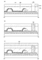
本発明の一態様の発光装置100の構成例について、図1を用いて説明する。図1(A)
は発光装置100の上面図であり、図1(B)は、図1(A)中でA1−A2の一点鎖線
で示す部位の断面図である。なお、本明細書に開示する発光装置100は、表示素子に発
光素子を用いた表示装置である。
A configuration example of the
1B is a top view of the
<発光装置の構成>
本実施の形態に示す発光装置100は、電極115、EL層117、電極118、隔壁1
14、および端子電極116を有する。電極115および端子電極116は電気的に接続
されている。また、発光装置100は、電極115上に隔壁114を有し、電極115お
よび隔壁114上にEL層117を有し、EL層117上に電極118を有している。
<Structure of light emitting device>
The light-emitting
14 and a
電極115、EL層117、および電極118により、発光素子125が形成される。ま
た、発光素子125は、基板111上に、接着層112、剥離層113、および下地層1
19を介して形成されている。なお、発光素子125は、表示領域131内に複数設けら
れている。
The
It is formed through nineteen. Note that a plurality of
また、本実施の形態に示す発光装置100は、電極118上に接着層120を介して基板
121が形成されている。また、基板121は、端子電極116と重畳する開口122a
を有する。また、接着層120は、開口122aと重畳する開口122bを有する。本明
細書では、開口122aおよび開口122bを併せて開口122と呼ぶ。開口122にお
いて、外部電極124と端子電極116が、異方性導電接続層123を介して電気的に接
続されている。
In the light-emitting
Have. The
また、発光素子125と端子電極116の間に、発光素子125に供給する信号を制御す
るスイッチング素子を設けてもよい。例えば、発光素子125と端子電極116の間に、
トランジスタを設けてもよい。
In addition, a switching element for controlling a signal supplied to the
A transistor may be provided.
トランジスタは半導体素子の一種であり、電流や電圧の増幅や、導通または非導通を制御
するスイッチング動作などを実現することができる。発光素子125と端子電極116の
間にトランジスタを設けることで、表示領域131の大面積化や、高精細化を容易とする
ことができる。なお、トランジスタなどのスイッチング素子に限らず、抵抗素子、インダ
クタ、キャパシタなどを表示領域131内に設けることもできる。
A transistor is a type of semiconductor element and can realize amplification of current or voltage, switching operation to control conduction or non-conduction, and the like. By providing the transistor between the light emitting
〔基板〕
基板121および基板111としては、有機樹脂材料や可撓性を有する程度の厚さのガラ
ス材料などを用いることができる。発光装置100を下面射出型の発光装置、または両面
射出型の発光装置とする場合には、基板111にEL層117からの発光に対して透光性
を有する材料を用いる。また、発光装置100を上面射出型の発光装置、または両面射出
型の発光装置とする場合には、基板121にEL層117からの発光に対して透光性を有
する材料を用いる。
〔substrate〕
As the
基板121および基板111に用いることができる可撓性及び可視光に対する透光性を有
する材料として、ポリエチレンテレフタレート樹脂、ポリエチレンナフタレート樹脂、ポ
リアクリロニトリル樹脂、ポリイミド樹脂、ポリメチルメタクリレート樹脂、ポリカーボ
ネート樹脂、ポリエーテルスルフォン樹脂、ポリアミド樹脂、シクロオレフィン樹脂、ポ
リスチレン樹脂、ポリアミドイミド樹脂、ポリ塩化ビニル樹脂、などを用いることができ
る。
As materials which can be used for the
また、基板121および基板111の熱膨張係数は、好ましくは30ppm/K以下、さ
らに好ましくは10ppm/K以下とする。また、基板121および基板111の表面に
、予め窒化シリコンや酸化窒化シリコン等の窒素と珪素を含む膜や窒化アルミニウム等の
窒素とアルミニウムを含む膜のような透水性の低い保護膜を成膜しておいても良い。なお
、基板121および基板111として、繊維体に有機樹脂が含浸された構造物(所謂、プ
リプレグとも言う)を用いてもよい。
Further, the thermal expansion coefficient of the
〔下地層〕
下地層119は、酸化シリコン、窒化シリコン、酸化窒化シリコン、窒化酸化シリコン、
酸化アルミニウム、酸化窒化アルミニウム、または窒化酸化アルミニウム等を、単層また
は多層で形成するのが好ましい。下地層119は、スパッタリング法やCVD法、熱酸化
法、塗布法、印刷法等を用いて形成することが可能である。
[Underlayer]
The
It is preferable to form aluminum oxide, aluminum oxynitride, or aluminum nitride oxide in a single layer or a multilayer. The
下地層119は、基板111や接着層112などから発光素子125への不純物元素の拡
散を防止、または低減することができる。
The
〔端子電極〕
端子電極116は、導電性を有する材料を用いて形成することができる。例えば、アルミ
ニウム、クロム、銅、銀、金、白金、タンタル、ニッケル、チタン、モリブデン、タング
ステン、ハフニウム(Hf)、バナジウム(V)、ニオブ(Nb)、マンガン、マグネシ
ウム、ジルコニウム、ベリリウム等から選ばれた金属元素、上述した金属元素を成分とす
る合金、または上述した金属元素を組み合わせた合金などを用いることができる。また、
リン等の不純物元素を含有させた多結晶シリコンに代表される半導体、ニッケルシリサイ
ドなどのシリサイドを用いてもよい。導電性を有する材料の形成方法は特に限定されず、
蒸着法、CVD法、スパッタリング法、スピンコート法などの各種形成方法を用いること
ができる。
[Terminal electrode]
The
A semiconductor typified by polycrystalline silicon containing an impurity element such as phosphorus or a silicide such as nickel silicide may be used. The method of forming the conductive material is not particularly limited.
Various formation methods such as a vapor deposition method, a CVD method, a sputtering method, and a spin coating method can be used.
また、端子電極116は、インジウム錫酸化物、酸化タングステンを含むインジウム酸化
物、酸化タングステンを含むインジウム亜鉛酸化物、酸化チタンを含むインジウム酸化物
、酸化チタンを含むインジウム錫酸化物、インジウム亜鉛酸化物、酸化ケイ素を添加した
インジウム錫酸化物などの酸素を含む導電性材料を適用することもできる。また、上記酸
素を含む導電性材料と、上記金属元素を含む材料の積層構造とすることもできる。
The
端子電極116は、単層構造でも、二層以上の積層構造としてもよい。例えば、シリコン
を含むアルミニウム層の単層構造、アルミニウム層上にチタン層を積層する二層構造、窒
化チタン層上にチタン層を積層する二層構造、窒化チタン層上にタングステン層を積層す
る二層構造、窒化タンタル層上にタングステン層を積層する二層構造、チタン層と、その
チタン層上にアルミニウム層を積層し、さらにその上にチタン層を形成する三層構造など
がある。また、アルミニウムに、チタン、タンタル、タングステン、モリブデン、クロム
、ネオジム、スカンジウムから選ばれた元素の層、または複数組み合わせた合金層、もし
くは窒化物層を用いてもよい。
The
〔電極115〕
電極115は、後に形成されるEL層117が発する光を効率よく反射する導電性材料を
用いて形成することが好ましい。なお、電極115は単層に限らず、複数層の積層構造と
してもよい。例えば、電極115を陽極として用いる場合、EL層117と接する層を、
インジウム錫酸化物などのEL層117よりも仕事関数が大きく透光性を有する層とし、
その層に接して反射率の高い層(アルミニウム、アルミニウムを含む合金、または銀など
)を設けてもよい。
[Electrode 115]
The
A work function is larger than that of the
A layer with high reflectance (eg, aluminum, an alloy containing aluminum, or silver) may be provided in contact with the layer.
なお、本実施の形態においては、トップエミッション構造の発光装置について例示するが
、ボトムエミッション構造(下面射出構造)、及びデュアルエミッション構造(両面射出
構造)の発光装置とする場合においては、電極115に透光性を有する導電性材料を用い
ればよい。
Note that although a light emitting device having a top emission structure is illustrated in this embodiment, in the case of using a light emitting device having a bottom emission structure (lower surface emission structure) or a dual emission structure (double surface emission structure), A conductive material having translucency may be used.
〔隔壁〕
隔壁114は、隣接する電極118間の電気的ショートを防止するために設ける。また、
後述するEL層117の形成にメタルマスクを用いる場合、メタルマスクが発光素子12
5を形成する領域に接触しないようにする機能も有する。隔壁114は、エポキシ樹脂、
アクリル樹脂、イミド樹脂などの有機樹脂材料や、酸化シリコンなどの無機材料で形成す
ることができる。隔壁114は、その側壁がテーパーまたは連続した曲率を持って形成さ
れる傾斜面となるように形成することが好ましい。隔壁114の側壁をこのような形状と
することで、後に形成されるEL層117や電極118の被覆性を良好なものとすること
ができる。
[Partition wall]
The
When a metal mask is used to form the
It also has a function of preventing contact with the area forming 5. The
It can be formed of an organic resin material such as acrylic resin or imide resin, or an inorganic material such as silicon oxide. The
〔EL層〕
EL層117の構成については、実施の形態9で説明する。
[EL layer]
The structure of the
〔電極118〕
本実施の形態では電極118を陰極として用いるため、電極118を後述するEL層11
7に電子を注入できる仕事関数の小さい材料を用いて形成することが好ましい。また、仕
事関数の小さい金属単体ではなく、仕事関数の小さいアルカリ金属、またはアルカリ土類
金属を数nm形成した層を緩衝層として形成し、その上にアルミニウムなどの金属材料、
インジウム錫酸化物等の導電性を有する酸化物材料、または半導体材料を用いて形成して
もよい。また、緩衝層として、アルカリ土類金属の酸化物、ハロゲン化物、または、マグ
ネシウム−銀等の合金を用いることもできる。
[Electrode 118]
In this embodiment mode, since the
It is preferable to form using a material with a small work function that can inject electrons into 7. In addition, a layer formed by forming a few nm of an alkali metal or alkaline earth metal having a small work function instead of a simple metal having a small work function is formed as a buffer layer, and a metal material such as aluminum is formed thereon.
A conductive oxide material such as indium tin oxide or a semiconductor material may be used. Further, as the buffer layer, an oxide of an alkaline earth metal, a halide, or an alloy such as magnesium-silver can also be used.
また、電極118を介して、EL層117が発する光を取り出す場合には、電極118は
、可視光に対し透光性を有することが好ましい。
In the case where light emitted from the
〔接着層〕
本実施の形態では、接着層120は、電極118に接して形成している。基板121は接
着層120により固定されている。また、接着層112は剥離層113に接して形成して
いる。基板111は接着層112により固定されている。接着層120および接着層11
2としては、光硬化型の接着剤、反応硬化型接着剤、熱硬化型接着剤、または嫌気型接着
剤を用いることができる。例えば、エポキシ樹脂、アクリル樹脂、イミド樹脂等を用いる
ことができる。トップエミッション構造の場合は接着層120に、ボトムエミッション構
造の場合は接着層112に、光の波長以下の大きさの乾燥剤(ゼオライト等)や、屈折率
の大きいフィラー(酸化チタンや、ジルコニウム等)を混合すると、EL層117が発す
る光の取り出し効率が向上するため好適である。
[Adhesive layer]
In the present embodiment, the
As 2, a photocurable adhesive, a reaction curable adhesive, a thermosetting adhesive, or an anaerobic adhesive can be used. For example, epoxy resin, acrylic resin, imide resin, etc. can be used. In the case of the top emission structure, the
〔剥離層〕
剥離層113は、タングステン、モリブデン、チタン、タンタル、ニオブ、ニッケル、コ
バルト、ジルコニウム、ルテニウム、ロジウム、パラジウム、オスミウム、イリジウム、
シリコンから選択された元素、または前記元素を含む合金材料、または前記元素を含む化
合物材料を用いて形成することができる。また、これらの材料を単層又は積層して形成す
ることができる。なお、剥離層113の結晶構造は、非晶質、微結晶、多結晶のいずれの
場合でもよい。また、剥離層113を、酸化アルミニウム、酸化ガリウム、酸化亜鉛、二
酸化チタン、酸化インジウム、酸化インジウムスズ、酸化インジウム亜鉛、またはInG
aZnO(IGZO)等の金属酸化物を用いて形成することもできる。
[Peeling layer]
The
It can be formed using an element selected from silicon, an alloy material containing the element, or a compound material containing the element. In addition, these materials can be formed in a single layer or stacked layers. Note that the crystal structure of the
It can also be formed using a metal oxide such as aZnO (IGZO).
剥離層113は、スパッタリング法やCVD法、塗布法、印刷法等により形成できる。な
お、塗布法はスピンコーティング法、液滴吐出法、ディスペンス法を含む。
The
剥離層113を単層で形成する場合、タングステン、モリブデン、またはタングステンと
モリブデンを含む合金材料を用いることが好ましい。または、剥離層113を単層で形成
する場合、タングステンの酸化物若しくは酸化窒化物、モリブデンの酸化物若しくは酸化
窒化物、またはタングステンとモリブデンを含む合金の酸化物若しくは酸化窒化物を用い
ることが好ましい。
In the case of forming the
また、剥離層113として、例えば、タングステンを含む層とタングステンの酸化物を含
む層の積層構造を形成する場合、タングステンを含む層に接して絶縁性酸化物層を形成す
ることで、タングステンを含む層と絶縁性酸化物層との界面に、酸化タングステンが形成
されることを活用してもよい。また、タングステンを含む層の表面を、熱酸化処理、酸素
プラズマ処理、オゾン水等の酸化力の強い溶液での処理等を行ってタングステンの酸化物
を含む層を形成してもよい。
Further, in the case of forming a stacked-layer structure of a layer containing tungsten and a layer containing an oxide of tungsten as the
〔異方性導電接続層〕
異方性導電接続層123は、様々な異方性導電フィルム(ACF:Anisotropi
c Conductive Film)や、異方性導電ペースト(ACP:Anisot
ropic Conductive Paste)などを用いて形成することができる。
[Anisotropic conductive connection layer]
The anisotropic
c Conductive Film and anisotropic conductive paste (ACP: Anisot
It can be formed using ropic conductive paste or the like.
異方性導電接続層123は、熱硬化性、又は熱硬化性及び光硬化性の樹脂に導電性粒子を
混ぜ合わせたペースト状又はシート状の材料を硬化させたものである。異方性導電接続層
123は、光照射や熱圧着によって異方性の導電性を示す材料となる。異方性導電接続層
123に用いられる導電性粒子としては、例えば球状の有機樹脂をAuやNi、Co等の
薄膜状の金属で被覆した粒子を用いることができる。
The anisotropic
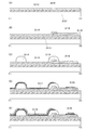
<発光装置の作製方法>
次に、図2乃至図6を用いて、発光装置100の作製方法を例示する。図2乃至図6は、
図1(A)中、A1−A2の一点鎖線で示す部位の断面に相当する。
<Method for manufacturing light emitting device>
Next, a method for manufacturing the light-emitting
This corresponds to the cross section of a portion indicated by an alternate long and short dash line A1-A2 in FIG.
〔剥離層の形成〕
まず、素子形成基板101上に剥離層113を形成する(図2(A)参照。)。なお、素
子形成基板101としては、ガラス基板、石英基板、サファイア基板、セラミック基板、
金属基板などを用いることができる。また、本実施の形態の処理温度に耐えうる耐熱性を
有するプラスチック基板を用いてもよい。
[Formation of Peeling Layer]
First, the
A metal substrate or the like can be used. Alternatively, a plastic substrate having heat resistance that can withstand the processing temperature of this embodiment may be used.
また、ガラス基板には、例えば、アルミノシリケートガラス、アルミノホウケイ酸ガラス
、バリウムホウケイ酸ガラスなどのガラス材料が用いられている。なお、酸化バリウム(
BaO)を多く含ませることで、より実用的な耐熱ガラスが得られる。他にも、結晶化ガ
ラスなどを用いることができる。
Further, as the glass substrate, for example, glass materials such as aluminosilicate glass, aluminoborosilicate glass, barium borosilicate glass and the like are used. In addition, barium oxide (
By containing a large amount of BaO), a more practical heat-resistant glass can be obtained. Besides, crystallized glass can be used.
本実施の形態では、剥離層113としてスパッタリング法によりタングステンを形成する
。
In this embodiment mode, tungsten is formed as the
〔下地層の形成〕
次に、剥離層113上に下地層119を形成する(図2(A)参照。)。本実施の形態で
は、下地層119としてプラズマCVD法により酸化シリコンを形成する。
[Formation of base layer]
Next, the
〔端子電極の形成〕
次に、下地層119上に端子電極116を形成する。まず、下地層119上に、スパッタ
リング法により二層のモリブデンの間にアルミニウムを挟んだ三層の金属膜を形成する。
続いて、金属膜上にレジストマスクを形成し、該レジストマスクを用いて、金属膜を所望
の形状にエッチングして端子電極116を形成することができる。レジストマスクの形成
は、フォトリソグラフィ法、印刷法、インクジェット法等を適宜用いて行うことができる
。レジストマスクをインクジェット法で形成するとフォトマスクを使用しないため、製造
コストを低減できる。
[Formation of terminal electrode]
Next, the
Subsequently, a resist mask is formed over the metal film, and the metal film can be etched into a desired shape using the resist mask to form the
金属膜のエッチングは、ドライエッチング法でもウェットエッチング法でもよく、両方を
用いてもよい。ウェットエッチング法により、金属膜のエッチングを行う場合は、エッチ
ング液として、燐酸と酢酸と硝酸を混ぜた溶液や、シュウ酸を含む溶液や、リン酸を含む
溶液などを用いることができる。エッチング処理終了後に、レジストマスクを除去する(
図2(B)参照)。
The metal film may be etched by either a dry etching method or a wet etching method, or both may be used. When etching a metal film by a wet etching method, a solution in which phosphoric acid, acetic acid, and nitric acid are mixed, a solution containing oxalic acid, a solution containing phosphoric acid, or the like can be used as an etching solution. After the etching process, remove the resist mask (
See FIG. 2 (B)).
〔電極115の形成〕
次に、下地層119上に電極115を形成する。電極115も端子電極116と同様に形
成することができる。本実施の形態では、電極115を、銀の上にインジウム錫酸化物を
積層した材料で形成する。電極115と端子電極116は電気的に接続されている(図2
(B)参照)。
[Formation of Electrode 115]
Next, the
(B)).
〔隔壁の形成〕
次に、隔壁114を形成する(図2(C)参照)。本実施の形態では、隔壁114を感光
性の有機樹脂材料を用いて塗布法で形成し、所望の形状に加工することにより形成する。
本実施の形態では、隔壁114を、感光性を有するイミド樹脂を用いて形成する。
[Formation of partition wall]
Next, the
In this embodiment mode, the
〔EL層の形成〕
次に、EL層117を電極115および隔壁114上に形成する(図2(D)参照)。
[Formation of EL layer]
Next, an
〔電極118の形成〕
次に、電極118をEL層117に接するように形成する。電極118は、蒸着法、スパ
ッタリング法等で形成することができる(図2(E)参照)。
[Formation of Electrode 118]
Next, the
〔基板の形成〕
次に、開口122aを有する基板121を、接着層120を介して電極118上に形成す
る。この時、基板121の開口122aを端子電極116と重畳するように配置する。ま
た、接着層120は、開口122aと重畳する領域に、開口122bを有する。前述した
通り、本明細書では、開口122aおよび開口122bを併せて開口122と呼ぶ(図3
(A)参照)。
[Formation of a substrate]
Next, a
(A)).
〔埋め込み層の形成〕
次に、開口122内に埋め込み層109を形成する(図3(B)参照)。開口122内に
埋め込み層109を形成しない場合、後の工程で行う素子形成基板101の剥離時に、端
子電極116の開口122と重畳する領域を損傷する恐れがある。なお、埋め込み層10
9は後に除去するため、水や有機溶剤に可溶な材料で形成することが好ましい。このよう
な材料として、可溶性アクリル樹脂、可溶性ポリイミド樹脂、可溶性エポキシ樹脂などの
可溶性樹脂を用いることができる。また、埋め込み層109の表面位置は、基板121の
表面と概略一致していることが好ましい。本実施の形態では、埋め込み層109として水
溶性のアクリル樹脂を用いる。
[Formation of buried layer]
Next, the buried
In order to remove 9 later, it is preferable to form with a soluble material in water or an organic solvent. As such a material, soluble resin such as soluble acrylic resin, soluble polyimide resin, soluble epoxy resin can be used. In addition, it is preferable that the surface position of the embedded
〔転載基板の形成〕
次に、転載基板102を、基板121上に貼り合わせる(図3(C)参照)。転載基板1
02は後に除去するため、転載基板102として、紫外線の照射により接着力が低下する
UVテープや、ダイシングテープ、または、加熱により接着力が低下するテープや、弱粘
性のテープを用いて形成することができる。本実施の形態では、転載基板102としてU
Vテープを用いる。
[Formation of reprinted substrate]
Next, the
Since 02 is to be removed later, the
Use V-tape.
〔基板の剥離〕
次に、素子形成基板101を剥離層113とともに下地層119から剥離する(図4(A
)参照)。剥離方法としては、機械的な力を加えること(人間の手や治具で引き剥がす処
理や、ローラーを回転させながら分離する処理、超音波等)を用いて行えばよい。たとえ
ば、剥離層113に鋭利な刃物またはレーザ光照射等で切り込みをいれ、その切り込みに
水を注入する。毛細管現象により水が剥離層113と下地層119の間にしみこむことに
より、素子形成基板101を容易に剥離することができる。
[Peeling of substrate]
Next, the
)reference). As a peeling method, mechanical force may be applied (processing of peeling off with a human hand or a jig, processing of separating while rotating a roller, ultrasonic waves, or the like). For example, a cut is made in the
〔発光装置と基板の貼り合わせ〕
次に、接着層112を介して基板111を下地層119に貼り合わせる(図4(B)参照
)。
[Lamination of light emitting device and substrate]
Next, the
〔転載基板の剥離〕
次に、転載基板102を剥離する。本実施の形態では転載基板102としてUVテープを
用いたため、転載基板102に紫外線103を照射することで(図5(A)参照)、転載
基板102を容易に剥離することができる(図5(B)参照)。
[Peeling of reprinted substrate]
Next, the
〔埋め込み層の除去〕
次に、水や有機溶剤などの、埋め込み層109の除去に適した溶剤を用いて埋め込み層1
09を除去する(図6(A)参照)。
[Removal of buried layer]
Next, using a solvent suitable for removing the buried
09 is removed (see FIG. 6A).
〔外部電極の形成〕
次に、開口122に異方性導電接続層123を形成する。また、開口122において端子
電極116と重畳する位置に、発光装置100に電力や信号を入力するための外部電極1
24を形成する(図6(B)参照)。外部電極124は、異方性導電接続層123を介し
て端子電極116と電気的に接続する。このようにして、発光装置100に電力や信号を
入力することが可能となる。なお、外部電極124として、FPCを用いることができる
。
[Formation of external electrode]
Next, the anisotropic
24 are formed (see FIG. 6 (B)). The
なお、外部電極124として金属線を用いることもできる。該金属線と端子電極116の
接続は、異方性導電接続層123を用いずに、ワイヤーボンディング法により行うことが
できる。また、該金属線と端子電極116の接続をハンダ付けにより行ってもよい。
Note that a metal wire can also be used as the
本発明の一態様によれば、発光装置100に電力や信号を入力するために、レーザ光や刃
物を用いて基板121の一部を除去する必要がないため、発光装置100や端子電極11
6にダメージを与えにくい。本発明の一態様によれば、作製歩留まりが良く、信頼性の良
好な発光装置を提供することができる。
According to one embodiment of the present invention, it is not necessary to remove part of the
Hard to damage 6 According to one embodiment of the present invention, a light-emitting device with high manufacturing yield and high reliability can be provided.
本実施の形態は、他の実施の形態に記載した構成と適宜組み合わせて実施することが可能
である。
This embodiment can be implemented in appropriate combination with the structures described in the other embodiments.
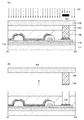
(実施の形態2)
本実施の形態では、実施の形態1で開示した方法と異なる方法で発光装置100を作製す
る方法について説明する。なお、説明の重複を防ぐため、本実施の形態では、主に実施の
形態1と異なる部分について説明する。
Second Embodiment
In this embodiment mode, a method for manufacturing the light-emitting
<発光装置の作製方法>
隔壁114の形成までは、実施の形態1と同様に行うことができる(図2(C)参照。)
<Method for manufacturing light emitting device>
The process up to the formation of the
〔EL層の形成〕
次に、EL層117を電極115および隔壁114上に形成する。この時、EL層117
の形成と同時に、端子電極116上の開口122と重畳する領域に層104を形成する(
図7(A)参照)。層104はEL層117と同じ材料および方法を用いて形成すること
ができる。
[Formation of EL layer]
Next, an
Simultaneously with forming the
7 (A)). The
〔電極118の形成〕
次に、電極118をEL層117に接するように形成する。この時、層104上の開口1
22と重畳する領域に層105を形成する。層105は、電極118と同じ層の一部を用
いて形成することができる(図7(B)参照)。
[Formation of Electrode 118]
Next, the
The
〔基板121の形成〕
次に、基板121を、接着層120を介して電極118上に形成する。この時、基板12
1の開口122を、端子電極116、層105、および層104と重畳するように配置す
る(図7(C)参照)。なお、接着層120は、開口122と重畳する領域には形成しな
いため、接着層120も開口122と重畳する開口を有する。
[Formation of Substrate 121]
Next, the
The one
なお、層104は、上面から見た時に、層104の外周部分が接着層の開口の外側に位置
する大きさで形成する。また、層105は、上面から見た時に、層105の外周部分が接
着層の開口の内側に位置する大きさで形成する。
The
〔埋め込み層と転載基板の形成〕
次に、実施の形態1と同様に、埋め込み層109と転載基板102を形成する(図7(D
)参照)。その後、素子形成基板101を剥離し、接着層112を介して基板111を貼
り合わせる。
[Formation of embedded layer and reprinted substrate]
Next, as in the first embodiment, the embedded
)reference). After that, the
〔転載基板の剥離〕
次に、転載基板102に紫外線103を照射し、転載基板102の接着力を弱めて転載基
板102を剥離する。紫外線103の照射に先立ち、埋め込み層109と重畳する領域に
マスク107を配置して、転載基板102の埋め込み層109と重畳する領域に紫外線1
03が照射されないようにする(図8(A)参照)。
[Peeling of reprinted substrate]
Next, the
It is made for 03 not to be irradiated (refer to FIG. 8 (A)).
このようにすることで、転載基板102の埋め込み層109と重畳する領域の接着力は、
低下せずに維持される。また、層104と層105の界面は密着性が低いので、転載基板
102の剥離と同時に、埋め込み層109と層105を除去することができる(図8(B
)参照)。
By doing this, the adhesion of the region overlapping the embedded
Maintained without decline. In addition, since the interface between the
)reference).
〔層104の除去〕
次に、エチルアルコールなどの有機溶剤を用いて、層104を除去し、端子電極116表
面の一部を露出させる(図9(A)参照)。
[Removal of layer 104]
Next, the
〔外部電極の形成〕
次に、開口122に異方性導電接続層123を形成し、異方性導電接続層123上に、発
光装置100に電力や信号を入力するための外部電極124を形成する(図9(B)参照
)。異方性導電接続層123を介して外部電極124と端子電極116を電気的に接続す
る。このようにして、発光装置100に電力や信号を入力することが可能となる。なお、
外部電極124として、FPCを用いることができる。
[Formation of external electrode]
Next, an anisotropic
As the
本発明の一態様によれば、発光装置100に電力や信号を入力するために、基板121の
一部を除去する必要がないため、発光装置100や端子電極116にダメージを与えにく
い。本発明の一態様によれば、作製歩留まりが良く、信頼性の良好な発光装置を提供する
ことができる。
According to one embodiment of the present invention, it is not necessary to remove part of the
本実施の形態は、他の実施の形態に記載した構成と適宜組み合わせて実施することが可能
である。
This embodiment can be implemented in appropriate combination with the structures described in the other embodiments.
(実施の形態3)
本実施の形態では、上記実施の形態に示した発光装置100と異なる構成を有する発光装
置200について、図10を用いて説明する。図10(A)は発光装置200の上面図で
あり、図10(B)は、図10(A)中でB1−B2の一点鎖線で示す部位の断面図であ
る。
Third Embodiment
In this embodiment, a light-emitting
<発光装置の構成>
本実施の形態に示す発光装置200は、表示領域231と、周辺回路251を有する。ま
た、発光装置200は、電極115、EL層117、電極118を含む発光素子125と
、端子電極216を有する。発光素子125は、表示領域231中に複数形成されている
。また、各発光素子125には、発光素子125の発光量を制御するトランジスタ232
が接続されている。
<Structure of light emitting device>
The light-emitting
Is connected.
端子電極216は、開口122に形成された異方性導電接続層123を介して外部電極1
24と電気的に接続されている。また、端子電極216は、周辺回路251に電気的に接
続されている。
The
It is electrically connected to 24. The
周辺回路251は、複数のトランジスタ252により構成されている。周辺回路251は
、外部電極124から供給された信号を、表示領域231中のどの発光素子125に供給
するかを決定する機能を有する。
The
図10に示す発光装置200は、接着層120を介して基板111と基板121が貼り合
わされた構造を有する。基板111上には、接着層112を介して絶縁層205が形成さ
れている。絶縁層205は、酸化シリコン、窒化シリコン、酸化窒化シリコン、窒化酸化
シリコン、酸化アルミニウム、酸化窒化アルミニウム、または窒化酸化アルミニウム等を
、単層または多層で形成するのが好ましい。絶縁層205は、スパッタリング法やCVD
法、熱酸化法、塗布法、印刷法等を用いて形成することが可能である。
The
It is possible to form using a method, a thermal oxidation method, a coating method, a printing method, or the like.
なお、絶縁層205は下地層として機能し、基板111や接着層112などからトランジ
スタや発光素子への不純物元素の拡散を防止、または低減することができる。
Note that the insulating
また、絶縁層205上に、トランジスタ232、トランジスタ252、端子電極216、
配線219が形成されている。なお、本実施の形態では、トランジスタ232およびトラ
ンジスタ252として、ボトムゲート型のトランジスタの1つであるチャネルエッチ型の
トランジスタを例示しているが、チャネル保護型のトランジスタやトップゲート型のトラ
ンジスタなどを用いることも可能である。また、チャネルが形成される半導体層を2つの
ゲート電極で挟む構造の、デュアルゲート型のトランジスタを用いることも可能である。
In addition, over the insulating
Wiring 219 is formed. Although a channel-etched transistor which is one of bottom-gate transistors is illustrated as the
トランジスタ232とトランジスタ252は、同様の構造を有していてもよい。ただし、
トランジスタのサイズ(例えば、チャネル長、およびチャネル幅)等は、各トランジスタ
で適宜調整することができる。
The
The size (eg, channel length and channel width) of the transistors can be adjusted as appropriate in each transistor.
トランジスタ232およびトランジスタ252は、ゲート電極206、ゲート絶縁層20
7、半導体層208、ソース電極209a、ドレイン電極209bを有する。
The
7, the
端子電極216、配線219、ゲート電極206、ソース電極209a、およびドレイン
電極209bは、端子電極116と同様の材料および方法により形成することができる。
また、ゲート絶縁層207は、絶縁層205と同様の材料および方法により形成すること
ができる。
The
The
半導体層208は、非晶質半導体、微結晶半導体、多結晶半導体等を用いて形成すること
ができる。例えば、非晶質シリコンや、微結晶ゲルマニウム等を用いることができる。ま
た、炭化シリコン、ガリウム砒素、酸化物半導体、窒化物半導体などの化合物半導体や、
有機半導体等を用いることができる。
The
An organic semiconductor or the like can be used.
なお、酸化物半導体は、エネルギーギャップが3.0eV以上と大きく、可視光に対する
透過率が大きい。また、酸化物半導体を適切な条件で加工して得られたトランジスタにお
いては、オフ電流を使用時の温度条件下(例えば、25℃)において、100zA(1×
10−19A)以下、もしくは10zA(1×10⁻²⁰A)以下、さらには1zA(1
×10−21A)以下とすることができる。このため、消費電力の少ない発光装置を提供
することができる。
Note that an oxide semiconductor has a large energy gap of 3.0 eV or more and a large transmittance to visible light. In addition, in a transistor obtained by processing an oxide semiconductor under appropriate conditions, an off-state current can be 100 zA (1 ×) at a temperature condition at use (eg, 25 ° C.)
10 −19 A) or less, or 10 zA (1 × 10 −20 A) or less, further 1 zA (1
× 10 -21 A) or less. Therefore, a light-emitting device with low power consumption can be provided.
また、半導体層208に酸化物半導体を用いる場合は、半導体層208に接する絶縁層に
酸素を含む絶縁層を用いることが好ましい。
In the case where an oxide semiconductor is used for the
また、トランジスタ232およびトランジスタ252上に絶縁層210が形成され、絶縁
層210上に絶縁層211が形成されている。絶縁層210は、保護絶縁層として機能し
、絶縁層210よりも上の層からトランジスタ232およびトランジスタ252への不純
物元素が拡散することを防止または低減することができる。絶縁層210は、絶縁層20
5と同様の材料及び方法で形成することができる。
In addition, the insulating
It can be formed by the same material and method as that of No.5.
また、発光素子125の被形成面の表面凹凸を低減するために絶縁層211に平坦化処理
を行ってもよい。平坦化処理としては、特に限定されないが、研磨処理(例えば、化学的
機械研磨法(Chemical Mechanical Polishing:CMP)
)、やドライエッチング処理により行うことができる。
Further, planarization treatment may be performed on the insulating
Or dry etching treatment.
また、平坦化機能を有する絶縁材料を用いて絶縁層211を形成することで、研磨処理を
省略することもできる。平坦化機能を有する絶縁材料として、例えば、ポリイミド樹脂、
アクリル樹脂等の有機材料を用いることができる。また上記有機材料の他に、低誘電率材
料(low−k材料)等を用いることができる。なお、これらの材料で形成される絶縁膜
を複数積層させることで、絶縁層211を形成してもよい。
In addition, the polishing process can be omitted by forming the insulating
An organic material such as acrylic resin can be used. In addition to the above organic materials, low dielectric constant materials (low-k materials) and the like can be used. Note that the insulating
また、絶縁層211上に、発光素子125と、各発光素子125を離間するための隔壁1
14が形成されている。
In addition, over the insulating
14 is formed.
また、基板121には、遮光膜264、着色層266、及びオーバーコート層268が形
成されている。発光装置200は、発光素子125からの光を、着色層266を介して基
板121側から射出する、所謂トップエミッション構造(上面射出構造)の発光装置であ
る。
In addition, a
また、発光素子125は、絶縁層211、および絶縁層210に設けられた開口でトラン
ジスタ232と電気的に接続されている。
In addition, the
また、本実施の形態では、発光装置の一例として、アクティブマトリクス型の発光装置に
ついて例示したが、パッシブマトリクス型の発光装置に適用することも可能である。
In addition, although an active matrix light-emitting device is illustrated as an example of a light-emitting device in this embodiment, the present invention can also be applied to a passive matrix light-emitting device.
また、本発明の一態様は、表示素子に発光素子を用いた発光装置に限らず、表示素子に液
晶素子を用いた液晶表示装置や、電子ペーパー、DMD(Digital Microm
irror Device)、PDP(Plasma Display Panel)、
FED(Field Emission Display)、SED(Surface−
conduction Electron−emitter Display)等の表示
装置に用いることも可能である。
Further, one embodiment of the present invention is not limited to a light emitting device using a light emitting element as a display element, and a liquid crystal display device using a liquid crystal element as a display element, electronic paper, DMD (Digital Microm
irror Device), PDP (Plasma Display Panel),
FED (Field Emission Display), SED (Surface-
It is also possible to use for display apparatuses, such as (Conduction Electron-emitter Display).
液晶素子の一例としては、液晶の光学的変調作用によって光の透過又は非透過を制御する
素子がある。その素子は一対の電極と液晶層により構造されることが可能である。なお、
液晶の光学的変調作用は、液晶にかかる電界(横方向の電界、縦方向の電界又は斜め方向
の電界を含む)によって制御される。なお、具体的には、液晶の一例としては、ネマチッ
ク液晶、コレステリック液晶、スメクチック液晶、ディスコチック液晶、サーモトロピッ
ク液晶、リオトロピック液晶、低分子液晶、高分子液晶、高分子分散型液晶(PDLC)
、強誘電液晶、反強誘電液晶、主鎖型液晶、側鎖型高分子液晶、バナナ型液晶などを挙げ
ることができる。また液晶の駆動方法としては、TN(Twisted Nematic
)モード、STN(Super Twisted Nematic)モード、IPS(I
n−Plane−Switching)モード、FFS(Fringe Field S
witching)モード、MVA(Multi−domain Vertical A
lignment)モード、PVA(Patterned Vertical Alig
nment)モード、ASV(Advanced Super View)モード、AS
M(Axially Symmetric aligned Micro−cell)モ
ード、OCB(Optically Compensated Birefringen
ce)モード、ECB(Electrically Controlled Biref
ringence)モード、FLC(Ferroelectric Liquid Cr
ystal)モード、AFLC(AntiFerroelectric Liquid
Crystal)モード、PDLC(Polymer Dispersed Liqui
d Crystal)モード、PNLC(Polymer Network Liqui
d Crystal)モード、ゲストホストモード、ブルー相(Blue Phase)
モードなどがある。ただし、これに限定されず、液晶素子及びその駆動方式として様々な
ものを用いることができる。
As an example of the liquid crystal element, there is an element which controls transmission or non-transmission of light by an optical modulation action of liquid crystal. The element can be constructed by a pair of electrodes and a liquid crystal layer. Note that
The optical modulation action of the liquid crystal is controlled by the electric field applied to the liquid crystal (including a horizontal electric field, a vertical electric field or an oblique electric field). Specifically, as an example of liquid crystal, nematic liquid crystal, cholesteric liquid crystal, smectic liquid crystal, discotic liquid crystal, thermotropic liquid crystal, lyotropic liquid crystal, low molecular liquid crystal, polymer liquid crystal, polymer dispersed liquid crystal (PDLC)
Examples thereof include ferroelectric liquid crystals, antiferroelectric liquid crystals, main chain liquid crystals, side chain polymer liquid crystals, and banana liquid crystals. As a method of driving the liquid crystal, TN (Twisted Nematic
), STN (Super Twisted Nematic) mode, IPS (I
n-Plane-Switching mode, FFS (Fringe Field S)
witching) mode, MVA (Multi-domain Vertical A)
lignment mode, PVA (Pattered Vertical Alig)
nment mode, ASV (Advanced Super View) mode, AS
M (Axially Symmetrically Aligned Micro-cell) mode, OCB (Optically Compensated Birefringen)
ce) mode, ECB (Electrically Controlled Biref
ringence mode, FLC (Ferroelectric Liquid Cr)
ystal) mode, AFLC (AntiFerroelectric Liquid
Crystal) mode, PDLC (Polymer Dispersed Liqui)
d Crystal mode, PNLC (Polymer Network Liqui)
d) Crystal mode, guest host mode, Blue Phase
There is a mode etc. However, the present invention is not limited to this, and various liquid crystal elements and driving methods thereof can be used.
電子ペーパーの表示方法の一例としては、分子により表示されるもの(光学異方性、染料
分子配向など)、粒子により表示されるもの(電気泳動、粒子移動、粒子回転、相変化な
ど)、フィルムの一端が移動することにより表示されるもの、分子の発色/相変化により
表示されるもの、分子の光吸収により表示されるもの、又は電子とホールが結合して自発
光により表示されるものなどを用いることができる。具体的には、電子ペーパーの表示方
法の一例としては、マイクロカプセル型電気泳動、水平移動型電気泳動、垂直移動型電気
泳動、球状ツイストボール、磁気ツイストボール、円柱ツイストボール方式、帯電トナー
、電子粉流体、磁気泳動型、磁気感熱式、エレクトロウェッテイング、光散乱(透明/白
濁変化)、コレステリック液晶/光導電層、コレステリック液晶、双安定性ネマチック液
晶、強誘電性液晶、2色性色素・液晶分散型、可動フィルム、ロイコ染料による発消色、
フォトクロミック、エレクトロクロミック、エレクトロデポジション、フレキシブル有機
ELなどがある。ただし、これに限定されず、電子ペーパー及びその表示方法として様々
なものを用いることができる。ここで、マイクロカプセル型電気泳動を用いることによっ
て、泳動粒子の凝集、沈殿を解決することができる。電子粉流体は、高速応答性、高反射
率、広視野角、低消費電力、メモリ性などのメリットを有する。
As an example of the display method of the electronic paper, those displayed by molecules (optical anisotropy, dye molecule orientation, etc.), those displayed by particles (electrophoresis, particle movement, particle rotation, phase change, etc.), film Displayed by moving one end of the, displayed by color development / phase change of the molecule, displayed by light absorption of the molecule, or displayed by self-emission by combining an electron and a hole Can be used. Specifically, as an example of a display method of electronic paper, microcapsule type electrophoresis, horizontal movement type electrophoresis, vertical movement type electrophoresis, spherical twist ball, magnetic twist ball, cylindrical twist ball system, charged toner, electron Powdered fluid, Magnetophoretic, Magnetic thermosensitive, Electrowetting, Light scattering (Transparent / white turbidity change), Cholesteric liquid crystal / photoconductive layer, Cholesteric liquid crystal, bistable nematic liquid crystal, ferroelectric liquid crystal, dichroic dye Liquid crystal dispersion type, movable film, color change with leuco dye,
There are photochromic, electrochromic, electrodeposition, flexible organic EL and the like. However, the present invention is not limited to this, and various kinds of electronic paper and its display method can be used. Here, aggregation and precipitation of electrophoretic particles can be solved by using microcapsule electrophoresis. The electronic powder fluid has advantages such as high-speed response, high reflectance, wide viewing angle, low power consumption, and memory performance.
本実施の形態は、他の実施の形態に記載した構成と適宜組み合わせて実施することが可能
である。
This embodiment can be implemented in appropriate combination with the structures described in the other embodiments.
(実施の形態4)
本発明の一態様の発光装置2100の構成例について、図11および図12を用いて説明
する。図11(A)は発光装置2100の外観を示す斜視図であり、図11(B)は、発
光装置2100の上面図である。また、図12は、図11においてC1−C2の一点鎖線
で示す部位の断面図である。なお、本明細書に開示する発光装置2100は、表示素子に
発光素子を用いた表示装置である。
Embodiment 4
A configuration example of the
<発光装置の構成>
本実施の形態に示す発光装置2100は、電極2115、EL層2117、電極2118
、隔壁2114、および端子電極2116を有する。電極2115および端子電極211
6は電気的に接続されている。また、発光装置2100は、電極2115上に隔壁211
4を有し、電極2115および隔壁2114上にEL層2117を有し、EL層2117
上に電極2118を有している。
<Structure of light emitting device>
The light-emitting
, A
6 are electrically connected. In addition, the
4 and has an
There is an
電極2115、EL層2117、および電極2118により、発光素子2125が形成さ
れる。また、発光素子2125は、基板2111上に、接着層2112、および下地層2
119を介して形成されている。なお、発光素子2125は、表示領域2131内に複数
設けられている。
The
119 is formed through. Note that a plurality of
また、本実施の形態に示す発光装置2100は、電極2118上に接着層2120を介し
て基板2121が形成されている。
In the light-emitting
また、下地層2119は、端子電極2116と重畳する開口2122aを有する。また、
接着層2112および基板2111は、開口2122aと重畳する開口2122bを有す
る。本明細書では、開口2122aおよび開口2122bを併せて開口2122と呼ぶ。
開口2122において、外部電極2124と端子電極2116が、異方性導電接続層21
23を介して電気的に接続されている。
The
The
In the
It is electrically connected through 23.
また、発光素子2125と端子電極2116の間に、発光素子2125に供給する信号を
制御するスイッチング素子を設けてもよい。例えば、発光素子2125と端子電極211
6の間に、トランジスタを設けてもよい。
In addition, a switching element for controlling a signal supplied to the
A transistor may be provided between six.
トランジスタは半導体素子の一種であり、電流や電圧の増幅や、導通または非導通を制御
するスイッチング動作などを実現することができる。発光素子2125と端子電極211
6の間にトランジスタを設けることで、表示領域2131の大面積化や、高精細化を容易
とすることができる。なお、トランジスタなどのスイッチング素子に限らず、抵抗素子、
インダクタ、キャパシタなどを表示領域2131内に設けることもできる。
A transistor is a type of semiconductor element and can realize amplification of current or voltage, switching operation to control conduction or non-conduction, and the like.
By providing the transistor between P.6, enlargement of the
Inductors, capacitors, and the like can also be provided in the
〔基板〕
基板2121および基板2111としては、上記実施の形態で開示した基板121および
基板111と同様の材料を用いることができる。発光装置2100を下面射出型の発光装
置、または両面射出型の発光装置とする場合には、基板2111にEL層2117からの
発光に対して透光性を有する材料を用いる。また、発光装置2100を上面射出型の発光
装置、または両面射出型の発光装置とする場合には、基板2121にEL層2117から
の発光に対して透光性を有する材料を用いる。
〔substrate〕
For the
〔下地層〕
下地層2119は、上記実施の形態で開示した下地層119と同様の材料および方法で形
成することができる。
[Underlayer]
The
下地層2119は、基板2111や接着層2112などから発光素子2125への不純物
元素の拡散を防止、または低減することができる。
The
〔端子電極〕
端子電極2116は、上記実施の形態で開示した端子電極116と同様の材料および方法
で形成することができる。
[Terminal electrode]
The
〔電極2115〕
電極2115は、後に形成されるEL層2117が発する光を効率よく反射する導電性材
料を用いて形成することが好ましい。電極2115は、上記実施の形態で開示した電極1
15と同様の材料および方法で形成することができる。
[Electrode 2115]
The
It can be formed by the same material and method as that of No. 15.
なお、本実施の形態においては、トップエミッション構造の発光装置について例示するが
、ボトムエミッション構造(下面射出構造)、及びデュアルエミッション構造(両面射出
構造)の発光装置とする場合においては、電極2115に透光性を有する導電性材料を用
いればよい。
Note that although a light emitting device with a top emission structure is illustrated in this embodiment, in the case of using a light emitting device with a bottom emission structure (lower surface emission structure) and a dual emission structure (double surface emission structure), A conductive material having translucency may be used.
〔隔壁〕
隔壁2114は、隣接する電極2118間の電気的ショートを防止するために設ける。ま
た、後述するEL層2117の形成にメタルマスクを用いる場合、メタルマスクが発光素
子2125を形成する領域に接触しないようにする機能も有する。隔壁2114は、上記
実施の形態で開示した隔壁114と同様の材料および方法で形成することができる。隔壁
2114は、その側壁がテーパーまたは連続した曲率を持って形成される傾斜面となるよ
うに形成することが好ましい。隔壁2114の側壁をこのような形状とすることで、後に
形成されるEL層2117や電極2118の被覆性を良好なものとすることができる。
[Partition wall]
The
〔EL層〕
EL層2117の構成については、実施の形態9で説明する。
[EL layer]
The structure of the
〔電極2118〕
本実施の形態では電極2118を陰極として用いるため、電極2118を後述するEL層
2117に電子を注入できる仕事関数の小さい材料を用いて形成することが好ましい。電
極2118は、上記実施の形態で開示した電極118と同様の材料および方法で形成する
ことができる。
[Electrode 2118]
In this embodiment mode, since the
また、電極2118を介して、EL層2117が発する光を取り出す場合には、電極21
18は、可視光に対し透光性を有することが好ましい。
In the case where light emitted from the
It is preferable that 18 have translucency to visible light.
〔接着層〕
本実施の形態では、接着層2120は、電極2118に接して形成している。基板212
1は接着層2120により固定されている。また、接着層2112は下地層2119に接
して形成している。基板2111は接着層2112により固定されている。接着層212
0および接着層2112としては、上記実施の形態で開示した接着層120および接着層
112と同様の材料および方法で形成することができる。また、トップエミッション構造
の場合は接着層2120に、ボトムエミッション構造の場合は接着層2112に、光の波
長以下の大きさの乾燥剤(ゼオライト等)や、屈折率の大きいフィラー(酸化チタンや、
ジルコニウム等)を混合すると、EL層2117が発する光の取り出し効率が向上するた
め好適である。
[Adhesive layer]
In this embodiment mode, the
1 is fixed by an
The 0 and the
It is preferable to mix zirconium and the like because the light extraction efficiency of the
〔異方性導電接続層〕
異方性導電接続層2123は、上記実施の形態で開示した異方性導電接続層123と同様
の材料および方法で形成することができる。
[Anisotropic conductive connection layer]
The anisotropic
<発光装置の作製方法>
次に、図13乃至図15を用いて、発光装置2100の作製方法を例示する。図13乃至
図15は、図11においてC1−C2の一点鎖線で示す部位の断面に相当する。
<Method for manufacturing light emitting device>
Next, a method for manufacturing the
〔剥離層の形成〕
まず、素子形成基板2101上に剥離層2113を形成する(図13(A)参照。)。な
お、素子形成基板2101としては、上記実施の形態で開示した素子形成基板101と同
様の材料を用いることができる。
[Formation of Peeling Layer]
First, the
剥離層2113は、上記実施の形態で開示した剥離層113と同様の材料および方法で形
成することができる。
The
本実施の形態では、剥離層2113としてスパッタリング法によりタングステンを形成す
る。
In this embodiment mode, tungsten is formed as the
〔下地層の形成〕
次に、剥離層2113上に下地層2119を形成する(図13(A)参照。)。本実施の
形態では、下地層2119としてプラズマCVD法により酸化シリコンを形成する。
[Formation of base layer]
Next, the
〔開口部の形成〕
次に、下地層2119の一部を選択的に除去し、開口2122aを形成する(図13(B
)参照。)。具体的には、下地層2119上にレジストマスクを形成し、該レジストマス
クを用いて、下地層2119の一部を選択的にエッチングする。レジストマスクの形成は
、フォトリソグラフィ法、印刷法、インクジェット法等を適宜用いて行うことができる。
レジストマスクをインクジェット法で形成するとフォトマスクを使用しないため、製造コ
ストを低減できる。また、下地層2119のエッチングは、ドライエッチング法でもウェ
ットエッチング法でもよく、両方を用いてもよい。下地層2119のエッチングは、剥離
層2113のエッチング速度よりも下地層2119のエッチング速度のほうが速い条件で
行うことが好ましい。
[Formation of opening]
Next, part of the
)reference. ). Specifically, a resist mask is formed over the
When the resist mask is formed by an inkjet method, a photomask is not used, and thus the manufacturing cost can be reduced. The
〔開口部の酸化処理〕
次に、開口2122aの形成により露出した剥離層2113表面を酸化させる。露出した
剥離層2113表面の酸化は、露出した剥離層2113表面に、過酸化水素水や、オゾン
を含有させた水などの、酸化力を有する溶液に触れさせることで行うことができる。また
、露出した剥離層2113表面を酸素雰囲気中に曝し、さらに紫外線を照射することで、
露出した剥離層2113表面を酸化させることができる。また、露出した剥離層2113
表面を酸素プラズマに曝してもよい。本実施の形態では、剥離層2113表面を酸素プラ
ズマ2126に曝すことにより、開口2122aの形成により露出した剥離層2113の
表面を酸化させる(図13(C)参照。)。
[Oxidation treatment of opening]
Next, the surface of the
The exposed
The surface may be exposed to oxygen plasma. In this embodiment, the surface of the
剥離層2113の表面に酸化層を形成することで、後の工程で行われる素子形成基板21
01の剥離を容易とすることができる。
By forming an oxide layer on the surface of the
The peeling of 01 can be made easy.
〔端子電極の形成〕
次に、下地層2119および開口2122aに重畳する端子電極2116を形成する(図
13(D)参照)。端子電極2116は、上記実施の形態で開示した端子電極116と同
様の材料および方法で形成することができる。
[Formation of terminal electrode]
Next, a
なお、開口2122aにおいて、剥離層2113と端子電極2116は、先の酸化処理に
より酸化された剥離層2113の表面を介して接している。剥離層2113と端子電極2
116の界面に酸化層を設けることで、後の工程で行われる素子形成基板2101の剥離
時に、端子電極2116が剥離層2113と一緒に剥がれてしまう現象を防ぐことができ
る。
Note that in the
By providing the oxide layer at the
〔電極2115の形成〕
次に、下地層2119上に電極2115を形成する。電極2115も端子電極2116と
同様に形成することができる。本実施の形態では、電極2115を、銀の上にインジウム
錫酸化物を積層した材料で形成する。また、電極2115と端子電極2116は電気的に
接続されている(図14(A)参照)。
[Formation of Electrode 2115]
Next, the
〔隔壁の形成〕
次に、隔壁2114を形成する(図14(B)参照)。本実施の形態では、隔壁2114
を感光性の有機樹脂材料を用いて塗布法で形成し、所望の形状に加工することにより形成
する。本実施の形態では、隔壁2114を、感光性を有するイミド樹脂を用いて形成する
。
[Formation of partition wall]
Next, the
Are formed by a coating method using a photosensitive organic resin material and processed into a desired shape. In this embodiment mode, the
〔EL層の形成〕
次に、EL層2117を電極2115および隔壁2114上に形成する(図14(C)参
照)。
[Formation of EL layer]
Next, an
〔電極2118の形成〕
次に、電極2118をEL層2117に接するように形成する。電極2118は、蒸着法
、スパッタリング法等で形成することができる(図14(D)参照)。
[Formation of Electrode 2118]
Next, an
〔基板2121の形成〕
次に、基板2121を、接着層2120を介して電極2118上に形成する(図15(A
)参照。)。
[Formation of Substrate 2121]
Next, a
)reference. ).
〔基板の剥離〕
次に、素子形成基板2101を剥離層2113とともに、下地層2119および端子電極
2116から剥離する(図15(B)参照)。剥離方法は、上記実施の形態で開示した基
板の剥離方法と同様に行うことができる。
[Peeling of substrate]
Next, the
〔発光装置と基板の貼り合わせ〕
次に、開口2122bを有する基板2111を、接着層2112を介して下地層2119
に貼り合わせる(図15(C)参照)。この時、基板2111の開口2122bを、開口
2122aと重畳する位置に配置する。また、接着層2112は、開口2122bと重畳
する領域には形成しない。なお、前述した通り、本明細書では、開口2122aおよび開
口2122bを併せて開口2122と呼ぶ。
[Lamination of light emitting device and substrate]
Next, the
(See FIG. 15C). At this time, the
〔外部電極の形成〕
次に、開口2122に異方性導電接続層2123を形成する。また、開口2122におい
て端子電極2116と重畳する位置に、発光装置2100に電力や信号を入力するための
外部電極2124を形成する(図12参照)。外部電極2124は、異方性導電接続層2
123を介して端子電極2116と電気的に接続される。このようにして、発光装置21
00に電力や信号を入力することが可能となる。なお、外部電極2124は、上記実施の
形態で開示した外部電極124と同様の材料および方法で形成することができる。
[Formation of external electrode]
Next, the anisotropic
It is electrically connected to the
It becomes possible to input power and signals at 00. Note that the
本発明の一態様によれば、レーザ光や刃物などを用いて基板2121の一部を除去する必
要がないため、表示領域2131や端子電極2116にダメージを与えにくい。また、表
示領域2131と開口2122までの距離を短くすることができるため、信号や電力の減
衰を少なくすることができる。また、作製工程が簡略化されるため、発光装置の生産性を
高めることができる。本発明の一態様によれば、作製歩留まりが良く、信頼性の良好な発
光装置を提供することができる。また、表示品位の良好な発光装置を提供することができ
る。
According to one embodiment of the present invention, since it is not necessary to remove part of the
<変形例>
また、本発明の一態様は、図16に示す発光装置2200のように構成することも可能で
ある。図16(A)は、発光装置2200の外観を示す斜視図であり、図16(B)は、
図16(A)におけるD1−D2の一点鎖線で示す部位の断面図である。
<Modification>
In addition, one embodiment of the present invention can be configured as a
It is sectional drawing of the site | part shown with the dashed-dotted line of D1-D2 in FIG. 16 (A).
発光装置2200は、発光装置2100とは基板2111の形状が異なる。発光装置22
00が有する基板2111は、開口2122bを有さない。また、基板2111は、開口
2122aと重畳しないように下地層2119に貼り合わされている。よって、図16に
示す発光装置2200は、基板2121と基板2111の端部が一致しない構成を有して
いる。
The
The
本実施の形態は、他の実施の形態に記載した構成と適宜組み合わせて実施することが可能
である。
This embodiment can be implemented in appropriate combination with the structures described in the other embodiments.
(実施の形態5)
本実施の形態では、上記実施の形態に示した発光装置2100と異なる構成を有する発光
装置2300について、図17を用いて説明する。図17(A)は発光装置2300の斜
視図であり、図17(B)は、図17(A)中でE1−E2の一点鎖線で示す部位の断面
図である。
Fifth Embodiment
In this embodiment, a light-emitting
<発光装置の構成>
本実施の形態に示す発光装置2300は、表示領域2231と、周辺回路2251を有す
る。また、発光装置2300は、電極2115、EL層2117、電極2118を含む発
光素子2125と、端子電極2216を有する。発光素子2125は、表示領域2231
中に複数形成されている。また、各発光素子2125には、発光素子2125の発光量を
制御するトランジスタ2232が接続されている。
<Structure of light emitting device>
The light-emitting
It is formed in plural. Further, each
端子電極2216は、開口2122に形成された異方性導電接続層2123を介して外部
電極2124と電気的に接続されている。また、端子電極2216は、周辺回路2251
に電気的に接続されている。
The
Are connected electrically.
周辺回路2251は、複数のトランジスタ2252により構成されている。周辺回路22
51は、外部電極2124から供給された信号を、表示領域2231中のどの発光素子2
125に供給するかを決定する機能を有する。図17(A)では、表示領域2231の外
側に4つの周辺回路2251を有する構成を示しているが、本発明の一態様はこれに限定
されない。
The
51 indicates the light-emitting
It has a function to determine whether to supply 125. Although FIG. 17A illustrates a structure in which four
図17に示す発光装置2300は、接着層2120を介して基板2111と基板2121
が貼り合わされた構造を有する。基板2111上には、接着層2112を介して絶縁層2
205が形成されている。絶縁層2205は、上記実施の形態で開示した絶縁層205と
同様の材料および方法で形成することができる。
A
Have a bonded structure. An insulating
205 is formed. The insulating
なお、絶縁層2205は下地層として機能し、基板2111や接着層2112などからト
ランジスタや発光素子への不純物元素の拡散を防止、または低減することができる。
Note that the insulating
また、絶縁層2205上に、トランジスタ2232、トランジスタ2252、端子電極2
216、配線2219が形成されている。なお、本実施の形態では、トランジスタ223
2およびトランジスタ2252として、ボトムゲート型のトランジスタの1つであるチャ
ネルエッチ型のトランジスタを例示しているが、チャネル保護型のトランジスタやトップ
ゲート型のトランジスタなどを用いることも可能である。
In addition, over the insulating
216 and a
Although a channel-etched transistor which is one of bottom-gate transistors is illustrated as the
トランジスタ2232とトランジスタ2252は、同様の構成を有する。ただし、トラン
ジスタのサイズ(例えば、チャネル長、およびチャネル幅)等は、各トランジスタで適宜
調整することができる。
The
トランジスタ2232およびトランジスタ2252は、ゲート電極2206、ゲート絶縁
層2207、半導体層2208、ソース電極2209a、ドレイン電極2209bを有す
る。
The
端子電極2216、配線2219、ゲート電極2206、ソース電極2209a、および
ドレイン電極2209bは、端子電極2116と同様の材料および方法により形成するこ
とができる。
また、ゲート絶縁層2207は、絶縁層2205と同様の材料および方法により形成する
ことができる。
The
The
半導体層2208は、上記実施の形態で開示した半導体層208と同様の材料および方法
で形成することができる。
The
また、半導体層2208に酸化物半導体を用いる場合は、半導体層2208に接する絶縁
層に酸素を含む絶縁層を用いることが好ましい。
In the case where an oxide semiconductor is used for the
また、トランジスタ2232およびトランジスタ2252上に絶縁層2210が形成され
、絶縁層2210上に絶縁層2211が形成されている。絶縁層2210は、保護絶縁層
として機能し、絶縁層2210よりも上の層からトランジスタ2232およびトランジス
タ2252へ不純物元素が拡散することを防止または低減することができる。絶縁層22
10は、絶縁層2205と同様の材料及び方法で形成することができる。
In addition, an insulating
10 can be formed by the same material and method as the insulating
また、発光素子2125の被形成面の表面凹凸を低減するために絶縁層2211に平坦化
処理を行ってもよい。平坦化処理としては、特に限定されないが、研磨処理(例えば、化
学的機械研磨法)、やドライエッチング処理により行うことができる。
Further, planarization treatment may be performed on the insulating
また、平坦化機能を有する絶縁材料を用いて絶縁層2211を形成することで、研磨処理
を省略することもできる。平坦化機能を有する絶縁材料として、例えば、ポリイミド樹脂
、アクリル樹脂等の有機材料を用いることができる。また上記有機材料の他に、低誘電率
材料(low−k材料)等を用いることができる。なお、これらの材料で形成される絶縁
膜を複数積層させることで、絶縁層2211を形成してもよい。
In addition, when the insulating
また、絶縁層2211上に、発光素子2125と、各発光素子2125を離間するための
隔壁2114が形成されている。
In addition, over the insulating
また、基板2121には、遮光膜2264、着色層2266、及びオーバーコート層22
68が形成されている。発光装置2300は、発光素子2125からの光を、着色層22
66を介して基板2121側から射出する、所謂トップエミッション構造(上面射出構造
)の発光装置である。
In addition, the
68 are formed. The
It is a light emitting device having a so-called top emission structure (upper surface emission structure), which emits light from the
また、発光素子2125は、絶縁層2211、および絶縁層2210に設けられた開口で
トランジスタ2232と電気的に接続されている。
The light-emitting
また、本実施の形態では、発光装置の一例として、アクティブマトリクス型の発光装置に
ついて例示したが、パッシブマトリクス型の発光装置に適用することも可能である。
In addition, although an active matrix light-emitting device is illustrated as an example of a light-emitting device in this embodiment, the present invention can also be applied to a passive matrix light-emitting device.
また、本発明の一態様は、表示素子に発光素子を用いた発光装置に限らず、表示素子に液
晶素子を用いた液晶表示装置や、電子ペーパー、DMD、PDP、FED、SED等の表
示装置に用いることも可能である。
One embodiment of the present invention is not limited to a light emitting device using a light emitting element as a display element, and a liquid crystal display device using a liquid crystal element as a display element, and a display device such as electronic paper, DMD, PDP, FED, SED, etc. It is also possible to use
液晶素子の一例としては、上記実施の形態に開示した液晶素子と同様の材料を用いること
ができる。また、液晶素子の駆動方法は、上記実施の形態に開示した液晶素子の駆動方法
と同様に行うことができる。
As an example of the liquid crystal element, the same material as the liquid crystal element disclosed in the above embodiment can be used. In addition, a method for driving a liquid crystal element can be performed in the same manner as the method for driving a liquid crystal element disclosed in the above embodiment.
また、電子ペーパーの表示方法は、上記実施の形態に開示した電子ペーパーの表示方法と
同様に行うことができる。
Further, the display method of the electronic paper can be performed in the same manner as the display method of the electronic paper disclosed in the above embodiment.
本実施の形態は、他の実施の形態に記載した構成と適宜組み合わせて実施することが可能
である。
This embodiment can be implemented in appropriate combination with the structures described in the other embodiments.
(実施の形態6)
本発明の一態様の発光装置3100の構成例について、図18乃至図20を用いて説明す
る。図18(A)は発光装置3100の斜視図であり、図18(B)は、図18(A)に
示す部位3150の拡大図である。また、図18(C)及び18(D)は、図18(A)
中でF1−F2に一点鎖線で示す部位の断面図である。なお、本明細書に開示する発光装
置3100は、表示素子に発光素子を用いた表示装置である。
Sixth Embodiment
Configuration examples of the light-emitting
It is sectional drawing of the part shown with a dashed-dotted line to F1-F2 in inside. Note that the light-emitting
<発光装置の構成>
本実施の形態に示す発光装置3100は、電極3115、EL層3117、電極3118
、隔壁3114、および端子電極3116を有する。電極3115および端子電極311
6は電気的に接続されている。また、発光装置3100は、電極3115上に隔壁311
4を有し、電極3115および隔壁3114上にEL層3117を有し、EL層3117
上に電極3118を有している。
<Structure of light emitting device>
The light-emitting
, A
6 are electrically connected. In addition, the
4 and has an
There is an
電極3115、EL層3117、および電極3118により、発光素子3125が形成さ
れる。また、発光素子3125は、基板3111上に、接着層3112、および下地層3
119を介して形成されている。なお、発光素子3125は、表示領域3131内に複数
設けられている。
A
119 is formed through. Note that a plurality of
また、本実施の形態に示す発光装置3100は、電極3118上に接着層3120を介し
て基板3121が形成されている。
In the light-emitting
基板3121は、溝部3141を有する。図18(A)乃至図18(C)に示す溝部31
41は、基板3121の厚さ方向に貫通しているが、溝部3141は、必ずしも基板31
21の厚さ方向に貫通している必要はない。溝部3141は、図18(D)に示すように
、基板3121を貫通せずに、一定の深さを有していてもよい。溝部3141が基板31
21を貫通しない場合の溝部3141の深さは、基板3121の厚さの2分の1以上が好
ましく、3分の2以上がより好ましい。なお、平面視において基板3121中の溝部31
41に囲まれた領域を部位3121aと呼ぶ。
The
41 penetrates in the thickness direction of the
It is not necessary to penetrate in the thickness direction of 21. The
The depth of the
A region surrounded by 41 is called a
また、端子電極3116上に層3104が形成され、層3104上に層3105が形成さ
れている。端子電極3116上の層3104および層3105は、部位3121aと重畳
する位置に形成される。
In addition, a
図19に示すように、部位3121aおよび部位3121aと重畳する接着層3120を
発光装置3100から分離することで、端子電極3116の一部を露出させることができ
る。図19(A)は、部位3121aおよび部位3121aと重畳する接着層3120の
分離途中の様子を示す斜視図であり、図19(B)は、部位3121aおよび部位312
1aと重畳する接着層3120の分離後の様子を示す斜視図である。また、図19(C)
は、図19(B)中にF1−F2の一点鎖線で示す部位の断面図である。
As illustrated in FIG. 19, part of the
It is a perspective view which shows the mode after isolation | separation of the
FIG. 19B is a cross-sectional view of a portion indicated by an alternate long and short dash line F1-F2 in FIG. 19B.
部位3121aおよび部位3121aと重畳する接着層3120を除去することで、開口
3122が形成され、端子電極3116の一部を露出させることができる。
By removing the
部位3121aと重畳する位置に層3104および層3105を設けることにより、部位
3121aを、部位3121aと重畳する接着層3120と一緒に容易に分離し、端子電
極3116を露出させることができる。なお、層3104および層3105については追
って詳述する。
By providing the
また、図20に示すように、開口3122において、外部電極3124と端子電極311
6が、異方性導電接続層3123を介して電気的に接続することができる。よって、基板
3121の開口3122と重畳する領域を「外部電極接続領域」ともいう。図20(A)
は外部電極3124が接続された発光装置3100の斜視図であり、図20(B)は、図
20(A)中にF1−F2の一点鎖線で示す部位の断面図である。
In addition, as shown in FIG. 20, in the
6 can be electrically connected through the anisotropic
20 is a perspective view of the
また、発光素子3125と端子電極3116の間に、発光素子3125に供給する信号を
制御するスイッチング素子を設けてもよい。例えば、発光素子3125と端子電極311
6の間に、トランジスタを設けてもよい。
In addition, a switching element for controlling a signal supplied to the
A transistor may be provided between six.
トランジスタは半導体素子の一種であり、電流や電圧の増幅や、導通または非導通を制御
するスイッチング動作などを実現することができる。発光素子3125と端子電極311
6の間にトランジスタを設けることで、表示領域3131の大面積化や、高精細化を容易
とすることができる。なお、トランジスタなどのスイッチング素子に限らず、抵抗素子、
インダクタ、キャパシタなどを表示領域3131内に設けることもできる。
A transistor is a type of semiconductor element and can realize amplification of current or voltage, switching operation to control conduction or non-conduction, and the like.
By providing the transistor between P.6, the
Inductors, capacitors, and the like can also be provided in the
〔基板〕
基板3111および基板3121としては、上記実施の形態で開示した基板121および
基板111と同様の材料を用いることができる。発光装置3100を下面射出型の発光装
置、または両面射出型の発光装置とする場合には、基板3111にEL層3117からの
発光に対して透光性を有する材料を用いる。また、発光装置3100を上面射出型の発光
装置、または両面射出型の発光装置とする場合には、基板3121にEL層3117から
の発光に対して透光性を有する材料を用いる。
〔substrate〕
For the
〔下地層〕
下地層3119は上記実施の形態で開示した下地層119と同様の材料および方法で形成
することができる。
[Underlayer]
The
下地層3119は、基板3111や接着層3112などから発光素子3125への不純物
元素の拡散を防止、または低減することができる。
The
〔端子電極〕
端子電極3116は、上記実施の形態で開示した端子電極116と同様の材料および方法
で形成することができる。
[Terminal electrode]
The
〔電極3115〕
電極3115は、後に形成されるEL層3117が発する光を効率よく反射する導電性材
料を用いて形成することが好ましい。電極3115は、上記実施の形態で開示した電極1
15と同様の材料および方法で形成することができる。
[Electrode 3115]
The
It can be formed by the same material and method as that of No. 15.
なお、本実施の形態においては、トップエミッション構造の発光装置について例示するが
、ボトムエミッション構造(下面射出構造)、及びデュアルエミッション構造(両面射出
構造)の発光装置とする場合においては、電極3115に透光性を有する導電性材料を用
いればよい。
Note that although a light emitting device having a top emission structure is illustrated in this embodiment, in the case of using a light emitting device having a bottom emission structure (lower surface emission structure) or a dual emission structure (double surface emission structure), the
〔隔壁〕
隔壁3114は、隣接する電極3118間の電気的ショートを防止するために設ける。ま
た、後述するEL層3117の形成にメタルマスクを用いる場合、メタルマスクが発光素
子3125を形成する領域に接触しないようにする機能も有する。隔壁3114は、上記
実施の形態で開示した隔壁114と同様の材料および方法で形成することができる。隔壁
3114は、その側壁がテーパーまたは連続した曲率を持って形成される傾斜面となるよ
うに形成することが好ましい。隔壁3114の側壁をこのような形状とすることで、後に
形成されるEL層3117や電極3118の被覆性を良好なものとすることができる。
[Partition wall]
The
〔EL層〕
EL層3117の構成については、実施の形態9で説明する。
[EL layer]
The structure of the
〔電極3118〕
本実施の形態では電極3118を陰極として用いるため、電極3118を後述するEL層
3117に電子を注入できる仕事関数の小さい材料を用いて形成することが好ましい。電
極3118は、上記実施の形態で開示した電極118と同様の材料および方法で形成する
ことができる。
[Electrode 3118]
In this embodiment mode, since the
また、電極3118を介して、EL層3117が発する光を取り出す場合には、電極31
18は、可視光に対し透光性を有することが好ましい。
When light emitted from the
It is preferable that 18 have translucency to visible light.
〔接着層〕
本実施の形態では、接着層3120は、電極3118に接して形成している。基板312
1は接着層3120により固定されている。また、基板3111は接着層3112により
固定されている。接着層3120および接着層3112としては、上記実施の形態で開示
した接着層120および接着層112と同様の材料および方法で形成することができる。
また、トップエミッション構造の場合は接着層3120に、ボトムエミッション構造の場
合は接着層3112に、光の波長以下の大きさの乾燥剤(ゼオライト等)や、屈折率の大
きいフィラー(酸化チタンや、ジルコニウム等)を混合すると、EL層3117が発する
光の取り出し効率が向上するため好適である。
[Adhesive layer]
In this embodiment mode, the
1 is fixed by the
In the case of the top emission structure, the
〔異方性導電接続層〕
異方性導電接続層3123は、上記実施の形態で開示した異方性導電接続層123と同様
の材料および方法で形成することができる。
[Anisotropic conductive connection layer]
The anisotropic
<発光装置の作製方法>
次に、図21乃至図24を用いて、発光装置3100の作製方法を例示する。図21乃至
図24は、図18乃至図20中、F1−F2の一点鎖線で示す部位の断面に相当する。
<Method for manufacturing light emitting device>
Next, a method for manufacturing the
〔剥離層の形成〕
まず、素子形成基板3101上に剥離層3113を形成する(図21(A)参照。)。な
お、素子形成基板3101としては、上記実施の形態で開示した素子形成基板101と同
様の材料を用いることができる。
[Formation of Peeling Layer]
First, the
剥離層3113は、上記実施の形態で開示した剥離層113と同様の材料および方法で形
成することができる。
The
本実施の形態では、剥離層3113としてスパッタリング法によりタングステンを形成す
る。
In this embodiment mode, tungsten is formed as the
〔下地層の形成〕
次に、剥離層3113上に下地層3119を形成する(図21(A)参照。)。本実施の
形態では、下地層3119としてプラズマCVD法により酸化シリコンを形成する。
[Formation of base layer]
Next, the
〔端子電極の形成〕
次に、下地層3119上に端子電極3116を形成する。まず、下地層3119上に、ス
パッタリング法により二層のモリブデンの間にアルミニウムを挟んだ三層の金属膜を形成
する。続いて、金属膜上にレジストマスクを形成し、該レジストマスクを用いて、金属膜
を所望の形状にエッチングして端子電極3116を形成することができる。レジストマス
クの形成は、フォトリソグラフィ法、印刷法、インクジェット法等を適宜用いて行うこと
ができる。レジストマスクをインクジェット法で形成するとフォトマスクを使用しないた
め、製造コストを低減できる。
[Formation of terminal electrode]
Next, the
金属膜のエッチングは、ドライエッチング法でもウェットエッチング法でもよく、両方を
用いてもよい。ウェットエッチング法により、金属膜のエッチングを行う場合は、エッチ
ング液として、燐酸と酢酸と硝酸を混ぜた溶液や、シュウ酸を含む溶液や、リン酸を含む
溶液などを用いることができる。エッチング処理終了後に、レジストマスクを除去する(
図21(B)参照)。
The metal film may be etched by either a dry etching method or a wet etching method, or both may be used. When etching a metal film by a wet etching method, a solution in which phosphoric acid, acetic acid, and nitric acid are mixed, a solution containing oxalic acid, a solution containing phosphoric acid, or the like can be used as an etching solution. After the etching process, remove the resist mask (
See FIG. 21 (B)).
〔電極の形成〕
次に、下地層3119上に電極3115を形成する。電極3115も端子電極3116と
同様に形成することができる。本実施の形態では、電極3115を、銀の上にインジウム
錫酸化物を積層した材料で形成する。電極3115と端子電極3116は電気的に接続さ
れている(図21(B)参照)。
[Formation of electrode]
Next, the
〔隔壁の形成〕
次に、隔壁3114を形成する(図21(C)参照)。本実施の形態では、隔壁3114
を感光性の有機樹脂材料を用いて塗布法で形成し、所望の形状に加工することにより形成
する。本実施の形態では、隔壁3114を、感光性を有するイミド樹脂を用いて形成する
。
[Formation of partition wall]
Next, the
Are formed by a coating method using a photosensitive organic resin material and processed into a desired shape. In this embodiment mode, the
〔EL層の形成〕
次に、EL層3117を電極3115および隔壁3114上に形成する。この時、EL層
3117の形成と同時に、端子電極3116上の開口3122と重畳する領域に層310
4を形成する(図21(D)参照)。層3104はEL層3117と同じ材料および方法
を用いて形成することができる。
[Formation of EL layer]
Next, an
4 are formed (see FIG. 21D). The
〔電極の形成〕
次に、電極3118をEL層3117に接するように形成する。この時、電極3118の
形成と同時に、層3104上の開口3122と重畳する領域に層3105を形成する。層
3105は電極3118と同じ層の一部を用いて形成することができる。電極3118お
よび層3105は、蒸着法、スパッタリング法等で形成することができる(図21(E)
参照)。
[Formation of electrode]
Next, an
reference).
〔基板の形成〕
次に、厚さ方向に貫通して形成された溝部3141を有する基板3121を、接着層31
20を介して電極3118上に形成する。この時、基板3121の部位3121aが、端
子電極3116、層3105、および層3104と重畳するように形成する。(図22(
A)参照)。
[Formation of a substrate]
Next, a
20 on the
See A).
なお、層3104は、上面から見た時に、層3104の外周部分が部位3121aの外側
に位置する大きさで形成する。また、層3105は、上面から見た時に、層3105の外
周部分が部位3121aの内側に位置する大きさで形成する。
Note that the
なお、溝部3141を一定の深さを有する溝とする場合は、溝部3141が形成されてい
ない基板3121を電極3118上に形成した後、鋭利な刃物やレーザ光を用いて、基板
3121に溝部3141を形成してもよい。
Note that in the case where the
この際、鋭利な刃物やレーザ光が基板3121を貫通すると、端子電極3116や他の部
位を損傷する恐れがある。よって、基板3121を電極3118上に形成した後に溝部3
141を形成する場合は、溝部3141が基板3121を貫通しないようにする必要があ
る。
At this time, if a sharp blade or a laser beam penetrates the
In the case of forming 141, it is necessary to prevent the
一方で、形成した溝部3141の深さが浅いと、後に行う部位3121aの分離がしにく
くなる。溝部3141が基板3121を貫通しない場合の溝部3141の深さは、基板3
121の厚さの2分の1以上が好ましく、3分の2以上がより好ましい。
On the other hand, when the depth of the formed
A half or more of the thickness of 121 is preferable, and 2/3 or more is more preferable.
〔基板の剥離〕
次に、素子形成基板3101を剥離層3113とともに下地層3119から剥離する(図
22(B)参照)。剥離方法は、上記実施の形態で開示した基板の剥離方法と同様に行う
ことができる。
[Peeling of substrate]
Next, the
〔発光装置と基板の貼り合わせ〕
次に、接着層3112を介して基板3111を下地層3119に貼り合わせる(図23(
A)参照)。このようにして、発光装置3100を作製することができる(図23(B)
参照)。
[Lamination of light emitting device and substrate]
Next, the
See A). Thus, the
reference).
続いて、端子電極3116と外部電極3124を電気的に接続させるための工程について
説明する。
Subsequently, steps for electrically connecting the
〔端子電極表面の露出〕
基板3121の部位3121a上に粘着テープを貼り、その後、粘着テープを剥がすよう
に引き上げると、部位3121aが溝部3141に沿って基板3121から分離する。こ
の時、層3104と層3105の界面は密着性が低いので、部位3121aの剥離と共に
部位3121aと重畳する接着層3120と層3105を除去することができる(図19
(A)、図24(A)参照)。
[Exposure of terminal electrode surface]
When an adhesive tape is attached onto the
(A) See FIG. 24 (A)).
なお、層3105は形成しなくても構わないが、接着層3120と層3104の界面に層
3105を設けると、部位3121aの分離時に、部位3121aと重畳する接着層31
20が発光装置3100側に残りにくい。よって、接着層3120と層3104の界面に
層3105を設けることで、作製歩留まりを向上させることができる。
Although the
20 does not easily remain on the
〔層3104の除去〕
次に、エチルアルコールなどの有機溶剤を用いて、層3104を除去し、端子電極311
6表面の一部を露出させる(図19(B)、図24(B)参照)。
[Removal of layer 3104]
Next, the
A part of the six surfaces is exposed (see FIG. 19B and FIG. 24B).
〔外部電極の形成〕
次に、開口3122に異方性導電接続層3123を形成し、異方性導電接続層3123上
に、発光装置3100に電力や信号を入力するための外部電極3124を形成する(図2
4(C)参照)。異方性導電接続層3123を介して外部電極3124と端子電極311
6を電気的に接続する。このようにして、発光装置3100に電力や信号を入力すること
が可能となる。なお、外部電極3124は、上記実施の形態で開示した外部電極124と
同様の材料および方法で形成することができる。
[Formation of external electrode]
Next, an anisotropic
4 (C)). The
Connect 6 electrically. In this manner, power and signals can be input to the
本発明の一態様によれば、基板3121に溝部3141を形成し、接着層3120と端子
電極3116の界面に層3104および層3105を形成することで、端子電極3116
の露出を容易とすることができる。よって、端子電極3116を露出させるために鋭利な
刃物等を用いて基板3121の一部をくり貫き除去する必要がないため、発光装置310
0や端子電極3116にダメージを与えにくい。
According to one embodiment of the present invention, the
Exposure can be facilitated. Therefore, it is not necessary to cut and remove a part of the
It is hard to damage 0 and the
また、層3104はEL層3117と同一行程で作製することができる。また、層310
5は電極3118と同一行程で作製することができる。よって、発光装置3100の作製
工程数を増加させることなく、部位3121aの除去を容易とすることができる。本発明
の一態様によれば、作製歩留まりが良く、信頼性の良好な発光装置を提供することができ
る。
The
5 can be manufactured in the same process as the
また、部位3121aは、端子電極3116を保護する機能を有する。部位3121aを
分離せずに発光装置3100の保管および搬送を行うことで、保管および搬送時に端子電
極3116を保護し、静電気等による発光装置3100の破損を防ぐことができる。
The
本実施の形態は、他の実施の形態に記載した構成と適宜組み合わせて実施することが可能
である。
This embodiment can be implemented in appropriate combination with the structures described in the other embodiments.
(実施の形態7)
図25(A)乃至図25(E)、および図26(A)乃至図26(E)は、基板3121
の端子電極3116と重畳する領域を拡大した平面図である。図25(A)乃至図25(
E)、および図26(A)乃至図26(E)に、溝部3141の配置例を示す。
Seventh Embodiment
FIGS. 25A to 25E and FIGS. 26A to 26E show a
15 is an enlarged plan view of a region overlapping with the
E) and FIG. 26 (A) to FIG. 26 (E) show arrangement examples of the
平面視において溝部3141に囲まれた領域が部位3121aである。言い換えると、溝
部3141は部位3121aの外周部に沿って形成される。溝部3141が基板3121
の厚さ方向に貫通して形成されている場合は、基板3121を基板3111上に貼り合せ
る前に基板3121から部位3121aが意図せず分離して、製造歩留まりを低下させる
ことを防ぐ必要がある。このため、部位3121aの外周に沿って、少なくとも2か所の
溝部3141が形成されていない領域(以下、「間隔a」という。)を形成する必要があ
る。
A region surrounded by the
It is necessary to prevent the
図25(A)乃至図25(E)、および図26(A)は、平面視において長方形の部位3
121aの外周に沿って溝部3141をミシン目状に形成する例を示している。なお、「
ミシン目」とは、切り離しし易いように断続的に形成された穴であり、溝部3141が穴
に相当する。
25 (A) to 25 (E) and 26 (A) show portions 3 of a rectangular shape in plan view.
The example which forms the
The “perforation” is a hole formed intermittently so as to be easily separated, and the
なお、溝部3141を基板3121の厚さ方向に貫通させない場合は、溝部3141をミ
シン目状に形成せずとも部位3121aの意図しない分離を防ぐことができる。よって、
溝部3141を基板3121の厚さ方向に貫通させない場合は、部位3121aの外周を
一つの溝部3141で囲うことができる。なお、基板3121の厚さ方向に貫通しない溝
部3141をミシン目状に形成してもよい。
In the case where the
When the
図25(A)は、部位3121aのそれぞれの短辺の両端部に溝部3141が形成されて
おらず、長辺に形成された溝部3141と短辺に形成された溝部3141は、間隔aによ
り分離している。
In FIG. 25A, the
図25(B)は、図25(A)の変形例であり、さらに部位3121aのそれぞれの長辺
を2つの溝部3141で形成した例を示している。
FIG. 25B is a modification of FIG. 25A, and further shows an example in which each long side of the
なお、間隔aの長さは、溝部3141の端部から隣接する溝部3141の端部までの最短
距離である。複数の溝部3141をミシン目状に配置する場合、間隔aが大きすぎると部
位3121aの分離が難しくなる。間隔aの長さは、基板3121の厚さの50倍以下が
好ましく、20倍以下がより好ましく、10倍以下がさらに好ましい。また、一つの溝部
3141の長さbは、より長い方が部位3121aの分離がしやすくなる。一つの溝部3
141の長さbは、間隔aの長さ以上とすることが好ましい。
The length of the gap a is the shortest distance from the end of the
The length b of 141 is preferably equal to or greater than the length of the interval a.
図25(C)は、図25(A)の他の変形例であり、それぞれの長辺を、一辺あたり8つ
の溝部3141で形成した例を示している。
FIG. 25C is another modification of FIG. 25A and shows an example in which each long side is formed of eight
図25(D)は、部位3121aの外周に配置された溝部3141が、四辺それぞれの中
央部分で分離されている例を示している。図25(D)は、4つのL字型の溝部3141
で長方形の部位3121aを形成する例を示している。
FIG. 25D shows an example in which the
Shows an example of forming a
図25(E)は、部位3121aの外周に溝部3141が形成され、2つの短辺のそれぞ
れの一部に間隔aを有する構成を例示している。図25(E)は、2つのL字型の溝部3
141で部位3121aを形成する例を示している。
FIG. 25E illustrates a configuration in which the
An example of forming the
図26(A)は、部位3121aの1つの長辺と1つの短辺をL字状の溝部3141とし
、他の二辺にミシン目状の溝部3141を形成する例を示している。
FIG. 26A shows an example in which one long side and one short side of the
図26(B)は、部位3121aを、平行に形成された2つの溝部3141の両端部に、
くの字型に折れ曲がった溝部3141を形成する例を示している。
In FIG. 26 (B), a
The example which forms the
図26(C)は、図26(B)の変形例であり、平行に形成された2つの溝部3141を
、それぞれ複数の溝部3141で形成する例を示している。
FIG. 26C is a modification of FIG. 26B, and shows an example in which two
図26(D)は、図26(B)の変形例であり、くの字型の溝部3141を円弧状の溝部
3141とする例を示している。
FIG. 26D is a modified example of FIG. 26B, and shows an example in which a V-shaped
図26(B)乃至図26(D)に示すように、平面視において部位3121aの端部に突
出した形状を付与することで、部位3121aの分離をさらに容易とすることができる。
As shown in FIGS. 26B to 26D, separation of the
なお、図26(E)に示すように、基板3121を横切って溝部3141を形成してもよ
い。ただし、発光装置3100の保管および搬送時に、保管器具や治具等と部位3121
aの端部が接触しやすくなるため、部位3121aの意図しない分離や、部分的なはがれ
が生じる恐れがある。また、部位3121aを分離して端子電極3116を露出させると
、当該領域すなわち外部電極接続領域の機械的強度が著しく低下するため、外部電極接続
領域が意図せず変形しやすく、発光装置3100の破損等が生じやすくなる。
Note that as shown in FIG. 26E, the
Unintended separation or partial peeling of the
一方、平面視において部位3121aを基板3121の端部より内側に設けることで、外
部電極接続領域の外周部分を基板3121と基板3111で支える構造とすることができ
る。このため、外部電極接続領域の機械的強度が低下しづらく、外部電極接続領域の意図
しない変形を軽減することができる。よって、発光装置3100の破損を防ぎ、発光装置
3100の信頼性を高めることができる。
On the other hand, by providing the
本実施の形態は、他の実施の形態に記載した構成と適宜組み合わせて実施することが可能
である。
This embodiment can be implemented in appropriate combination with the structures described in the other embodiments.
(実施の形態8)
本実施の形態では、上記実施の形態に示した発光装置3100と異なる構成を有する発光
装置3200について、図27を用いて説明する。図27(A)は発光装置3200の上
面図であり、図27(B)は、図27(A)中でG1−G2の一点鎖線で示す部位の断面
図である。
Eighth Embodiment
In this embodiment, a light-emitting
<発光装置の構成>
本実施の形態に示す発光装置3200は、表示領域3231と、周辺回路3251を有す
る。また、発光装置3200は、電極3115、EL層3117、電極3118を含む発
光素子3125と、端子電極3216を有する。発光素子3125は、表示領域3231
中に複数形成されている。また、各発光素子3125には、発光素子3125の発光量を
制御するトランジスタ3232が接続されている。
<Structure of light emitting device>
The light-emitting
It is formed in plural. In addition, a
端子電極3216は、開口3122に形成された異方性導電接続層3123を介して外部
電極3124と電気的に接続されている。また、端子電極3216は、周辺回路3251
に電気的に接続されている。
The
Are connected electrically.
周辺回路3251は、複数のトランジスタ3252により構成されている。周辺回路32
51は、外部電極3124から供給された信号を、表示領域3231中のどの発光素子3
125に供給するかを決定する機能を有する。
The
51 indicates the light-emitting element 3 in the
It has a function to determine whether to supply 125.
図27に示す発光装置3200は、接着層3120を介して基板3111と基板3121
が貼り合わされた構造を有する。基板3111上には、接着層3112を介して絶縁層3
205が形成されている。絶縁層3205は、上記実施の形態で開示した絶縁層205と
同様の材料および方法で形成することができる。
A
Have a bonded structure. An insulating layer 3 is formed on the
205 is formed. The insulating
なお、絶縁層3205は下地層として機能し、基板3111や接着層3112などからト
ランジスタや発光素子への不純物元素の拡散を防止、または低減することができる。
Note that the insulating
また、絶縁層3205上に、トランジスタ3232、トランジスタ3252、端子電極3
216、配線3219が形成されている。なお、本実施の形態では、トランジスタ323
2およびトランジスタ3252として、ボトムゲート型のトランジスタの1つであるチャ
ネルエッチ型のトランジスタを例示しているが、チャネル保護型のトランジスタや、トッ
プゲート型のトランジスタなどを用いることも可能である。また、チャネルが形成される
半導体層を2つのゲート電極で挟む構造の、デュアルゲート型のトランジスタを用いるこ
とも可能である。
In addition, over the insulating
216 and a
Although a channel-etched transistor which is one of bottom-gate transistors is illustrated as the
トランジスタ3232とトランジスタ3252は、同様の構造を有していてもよい。ただ
し、トランジスタのサイズ(例えば、チャネル長、およびチャネル幅)等は、各トランジ
スタで適宜調整することができる。
The
トランジスタ3232およびトランジスタ3252は、ゲート電極3206、ゲート絶縁
層3207、半導体層3208、ソース電極3209a、ドレイン電極3209bを有す
る。
The
端子電極3216、配線3219、ゲート電極3206、ソース電極3209a、および
ドレイン電極3209bは、端子電極3116と同様の材料および方法により形成するこ
とができる。また、ゲート絶縁層3207は、絶縁層3205と同様の材料および方法に
より形成することができる。
The
半導体層3208は、上記実施の形態で開示した半導体層208と同様の材料および方法
で形成することができる。
The
また、半導体層3208に酸化物半導体を用いる場合は、半導体層3208に接する絶縁
層に酸素を含む絶縁層を用いることが好ましい。
In the case where an oxide semiconductor is used for the
また、トランジスタ3232およびトランジスタ3252上に絶縁層3210が形成され
、絶縁層3210上に絶縁層3211が形成されている。絶縁層3210は、保護絶縁層
として機能し、絶縁層3210よりも上の層からトランジスタ3232およびトランジス
タ3252へ不純物元素が拡散することを防止または低減することができる。絶縁層32
10は、絶縁層3205と同様の材料及び方法で形成することができる。
In addition, the insulating
10 can be formed by the same material and method as the insulating
また、発光素子3125の被形成面の表面凹凸を低減するために絶縁層3211に平坦化
処理を行ってもよい。平坦化処理としては、特に限定されないが、研磨処理(例えば、化
学的機械研磨法)、やドライエッチング処理により行うことができる。
Further, planarization treatment may be performed on the insulating
また、平坦化機能を有する絶縁材料を用いて絶縁層3211を形成することで、研磨処理
を省略することもできる。平坦化機能を有する絶縁材料として、例えば、ポリイミド樹脂
、アクリル樹脂等の有機材料を用いることができる。また上記有機材料の他に、低誘電率
材料(low−k材料)等を用いることができる。なお、これらの材料で形成される絶縁
膜を複数積層させることで、絶縁層3211を形成してもよい。
In addition, polishing treatment can be omitted by forming the insulating
また、絶縁層3211上に、発光素子3125と、各発光素子3125を離間するための
隔壁3114が形成されている。
In addition, over the insulating
また、基板3121には、遮光膜3264、着色層3266、及びオーバーコート層32
68が形成されている。発光装置3200は、発光素子3125からの光を、着色層32
66を介して基板3121側から射出する、所謂トップエミッション構造(上面射出構造
)の発光装置である。
In addition, a
68 are formed. The
It is a light emitting device having a so-called top emission structure (upper surface emission structure) which emits light from the side of the
また、発光素子3125は、絶縁層3211、および絶縁層3210に設けられた開口で
トランジスタ3232と電気的に接続されている。
The light-emitting
また、本実施の形態では、発光装置の一例として、アクティブマトリクス型の発光装置に
ついて例示したが、パッシブマトリクス型の発光装置に適用することも可能である。
In addition, although an active matrix light-emitting device is illustrated as an example of a light-emitting device in this embodiment, the present invention can also be applied to a passive matrix light-emitting device.
また、本発明の一態様は、表示素子に発光素子を用いた発光装置に限らず、表示素子に液
晶素子を用いた液晶表示装置や、電子ペーパー、DMD、PDP、FED、SED等の表
示装置に用いることも可能である。
One embodiment of the present invention is not limited to a light emitting device using a light emitting element as a display element, and a liquid crystal display device using a liquid crystal element as a display element, and a display device such as electronic paper, DMD, PDP, FED, SED, etc. It is also possible to use
液晶素子の一例としては、上記実施の形態に開示した液晶素子と同様の材料を用いること
ができる。また、液晶素子の駆動方法は、上記実施の形態に開示した液晶素子の駆動方法
と同様に行うことができる。
As an example of the liquid crystal element, the same material as the liquid crystal element disclosed in the above embodiment can be used. In addition, a method for driving a liquid crystal element can be performed in the same manner as the method for driving a liquid crystal element disclosed in the above embodiment.
また、電子ペーパーの表示方法は、上記実施の形態に開示した電子ペーパーの表示方法と
同様に行うことができる。
Further, the display method of the electronic paper can be performed in the same manner as the display method of the electronic paper disclosed in the above embodiment.
本実施の形態は、他の実施の形態に記載した構成と適宜組み合わせて実施することが可能
である。
This embodiment can be implemented in appropriate combination with the structures described in the other embodiments.
(実施の形態9)
本実施の形態では、発光素子125、発光素子2125、および発光素子3125に用い
ることができる発光素子の構成例について説明する。なお、本実施の形態に示すEL層3
20が、上記実施の形態に示したEL層117、EL層2117、およびEL層3117
に相当する。
(Embodiment 9)
In this embodiment, a structural example of a light-emitting element that can be used for the light-emitting
20 are the
It corresponds to
<発光素子の構成>
図28(A)に示す発光素子330は、一対の電極(第1の電極318、第2の電極32
2)間にEL層320が挟まれた構造を有する。なお、以下の本実施の形態の説明におい
ては、例として、第1の電極318を陽極として用い、第2の電極322を陰極として用
いるものとする。
<Structure of Light Emitting Element>
A
2) The
また、EL層320は、少なくとも発光層を含んで形成されていればよく、発光層以外の
機能層を含む積層構造であっても良い。発光層以外の機能層としては、正孔注入性の高い
物質、正孔輸送性の高い物質、電子輸送性の高い物質、電子注入性の高い物質、バイポー
ラ性(電子及び正孔の輸送性の高い物質)の物質等を含む層を用いることができる。具体
的には、正孔注入層、正孔輸送層、電子輸送層、電子注入層等の機能層を適宜組み合わせ
て用いることができる。
The
図28(A)に示す発光素子330は、第1の電極318と第2の電極322との間に生
じた電位差により電流が流れ、EL層320において正孔と電子とが再結合し、発光する
ものである。つまりEL層320に発光領域が形成されるような構成となっている。
In the light-emitting
本発明において、発光素子330からの発光は、第1の電極318、または第2の電極3
22側から外部に取り出される。従って、第1の電極318、または第2の電極322の
いずれか一方は透光性を有する物質で成る。
In the present invention, light emission from the
It is taken out from the 22 side. Therefore, one of the
なお、EL層320は図28(B)に示す発光素子331のように、第1の電極318と
第2の電極322との間に複数積層されていても良い。n層(nは2以上の自然数)の積
層構造を有する場合には、m番目(mは、1≦m<nを満たす自然数)のEL層320と
、(m+1)番目のEL層320との間には、それぞれ電荷発生層320aを設けること
が好ましい。
Note that a plurality of EL layers 320 may be stacked between the
電荷発生層320aは、有機化合物と金属酸化物の複合材料、金属酸化物、有機化合物と
アルカリ金属、アルカリ土類金属、またはこれらの化合物との複合材料の他、これらを適
宜組み合わせて形成することができる。有機化合物と金属酸化物の複合材料としては、例
えば、有機化合物と酸化バナジウムや酸化モリブデンや酸化タングステン等の金属酸化物
を含む。有機化合物としては、芳香族アミン化合物、カルバゾール誘導体、芳香族炭化水
素等の低分子化合物、または、高分子化合物(オリゴマー、デンドリマー、ポリマー等)
など、種々の化合物を用いることができる。なお、有機化合物としては、正孔輸送性有機
化合物として正孔移動度が10−6cm2/Vs以上であるものを適用することが好まし
い。但し、電子よりも正孔の輸送性の高い物質であれば、これら以外のものを用いてもよ
い。なお、電荷発生層320aに用いるこれらの材料は、キャリア注入性、キャリア輸送
性に優れているため、発光素子330の低電流駆動、および低電圧駆動を実現することが
できる。
The
Various compounds can be used. In addition, as an organic compound, it is preferable to apply the thing whose hole mobility is 10 <-6 > cm < 2 > / Vs or more as a hole transportable organic compound. However, any substance other than these may be used as long as the substance has a hole transportability higher than that of electrons. Note that since these materials used for the
なお、電荷発生層320aは、有機化合物と金属酸化物の複合材料と他の材料とを組み合
わせて形成してもよい。例えば、有機化合物と金属酸化物の複合材料を含む層と、電子供
与性物質の中から選ばれた一の化合物と電子輸送性の高い化合物とを含む層とを組み合わ
せて形成してもよい。また、有機化合物と金属酸化物の複合材料を含む層と、透明導電膜
とを組み合わせて形成してもよい。
Note that the
このような構成を有する発光素子331は、エネルギーの移動や消光などの問題が起こり
難く、材料の選択の幅が広がることで高い発光効率と長い寿命とを併せ持つ発光素子とす
ることが容易である。また、一方のEL層で燐光発光、他方で蛍光発光を得ることも容易
である。
The
なお、電荷発生層320aとは、第1の電極318と第2の電極322に電圧を印加した
ときに、電荷発生層320aに接して形成される一方のEL層320に対して正孔を注入
する機能を有し、他方のEL層320に電子を注入する機能を有する。
Note that in the
図28(B)に示す発光素子331は、EL層320に用いる発光物質の種類を変えるこ
とにより様々な発光色を得ることができる。また、発光物質として発光色の異なる複数の
発光物質を用いることにより、ブロードなスペクトルの発光や白色発光を得ることもでき
る。
The light-emitting
図28(B)に示す発光素子331を用いて、白色発光を得る場合、複数のEL層の組み
合わせとしては、赤、青及び緑色の光を含んで白色に発光する構成であればよく、例えば
、青色の蛍光材料を発光物質として含む第1の発光層と、緑色と赤色の燐光材料を発光物
質として含む第2の発光層を有する構成が挙げられる。また、赤色の発光を示す第1の発
光層と、緑色の発光を示す第2の発光層と、青色の発光を示す第3の発光層とを有する構
成とすることもできる。または、補色の関係にある光を発する発光層を有する構成であっ
ても白色発光が得られる。発光層が2層積層された積層型素子において、第1の発光層か
ら得られる発光の発光色と第2の発光層から得られる発光の発光色を補色の関係にする場
合、補色の関係としては、青色と黄色、あるいは青緑色と赤色などが挙げられる。
When white light emission is obtained using the light-emitting
なお、上述した積層型素子の構成において、積層される発光層の間に電荷発生層を配置す
ることにより、電流密度を低く保ったまま、高輝度領域での長寿命素子を実現することが
できる。また、電極材料の抵抗による電圧降下を小さくできるので、大面積での均一な発
光が可能となる。
In the above-described structure of the stacked element, by disposing the charge generation layer between the light emitting layers to be stacked, a long life element can be realized in a high luminance region while keeping the current density low. . In addition, since the voltage drop due to the resistance of the electrode material can be reduced, uniform light emission over a large area is possible.
本実施の形態は、他の実施の形態に記載した構成と適宜組み合わせて実施することが可能
である。
This embodiment can be implemented in appropriate combination with the structures described in the other embodiments.
(実施の形態10)
本実施の形態では、本発明の一態様の発光装置が適用された電子機器や照明装置の例につ
いて、図面を参照して説明する。
Tenth Embodiment
In this embodiment, examples of electronic devices and lighting devices to which the light-emitting device of one embodiment of the present invention is applied will be described with reference to the drawings.
フレキシブルな形状を備える発光装置を適用した電子機器として、例えば、テレビジョン
装置(テレビ、又はテレビジョン受信機ともいう)、コンピュータ用などのモニタ、デジ
タルカメラ、デジタルビデオカメラ、デジタルフォトフレーム、携帯電話機(携帯電話、
携帯電話装置ともいう)、携帯型ゲーム機、携帯情報端末、音響再生装置、パチンコ機な
どの大型ゲーム機などが挙げられる。
As an electronic device to which a light-emitting device having a flexible shape is applied, for example, a television (also referred to as a television or a television receiver), a monitor for a computer, a digital camera, a digital video camera, a digital photo frame, a mobile phone (mobile phone,
Examples include large-sized game machines such as portable game machines, portable information terminals, sound reproduction devices, and pachinko machines.
また、照明や表示装置を、家屋やビルの内壁または外壁や、自動車の内装または外装の曲
面に沿って組み込むことも可能である。
It is also possible to incorporate lighting and display devices along the inner or outer wall of a house or building, or along the curved surface of the interior or exterior of a car.
図29(A)は、携帯電話機の一例を示している。携帯電話機7400は、筐体7401
に組み込まれた表示部7402の他、操作ボタン7403、外部接続ポート7404、ス
ピーカ7405、マイク7406などを備えている。なお、携帯電話機7400は、発光
装置を表示部7402に用いることにより作製される。
FIG. 29A shows an example of a mobile phone. The
In addition to the
図29(A)に示す携帯電話機7400は、表示部7402を指などで触れることで、情
報を入力することができる。また、電話を掛ける、或いは文字を入力するなどのあらゆる
操作は、表示部7402を指などで触れることにより行うことができる。
Information can be input to the
また操作ボタン7403の操作により、電源のON、OFFや、表示部7402に表示さ
れる画像の種類を切り替えることができる。例えば、メール作成画面から、メインメニュ
ー画面に切り替えることができる。
By operating the
ここで、表示部7402には、本発明の一態様の発光装置が組み込まれている。したがっ
て、湾曲した表示部を備え、且つ信頼性の高い携帯電話機とすることができる。
Here, the light-emitting device of one embodiment of the present invention is incorporated in the
図29(B)は、リストバンド型の表示装置の一例を示している。携帯表示装置7100
は、筐体7101、表示部7102、操作ボタン7103、及び送受信装置7104を備
える。
FIG. 29B illustrates an example of a wristband display device.
Includes a housing 7101, a
携帯表示装置7100は、送受信装置7104によって映像信号を受信可能で、受信した
映像を表示部7102に表示することができる。また、音声信号を他の受信機器に送信す
ることもできる。
The
また、操作ボタン7103によって、電源のON、OFF動作や表示する映像の切り替え
、または音声のボリュームの調整などを行うことができる。
In addition, with the
ここで、表示部7102には、本発明の一態様の発光装置が組み込まれている。したがっ
て、湾曲した表示部を備え、且つ信頼性の高い携帯表示装置とすることができる。
Here, the light-emitting device of one embodiment of the present invention is incorporated in the
図29(C)乃至図29(E)は、照明装置の一例を示している。照明装置7200、照
明装置7210、照明装置7220はそれぞれ、操作スイッチ7203を備える台部72
01と、台部7201に支持される発光部を有する。
29C to 29E illustrate an example of a lighting device. The
And a light emitting unit supported by a
図29(C)に示す照明装置7200は、波状の発光面を有する発光部7202を備える
。したがってデザイン性の高い照明装置となっている。
The
図29(D)に示す照明装置7210の備える発光部7212は、凸状に湾曲した2つの
発光部が対称的に配置された構成となっている。したがって照明装置7210を中心に全
方位を照らすことができる。
The
図29(E)に示す照明装置7220は、凹状に湾曲した発光部7222を備える。した
がって、発光部7222からの発光を、照明装置7220の前面に集光するため、特定の
範囲を明るく照らす場合に適している。
The
また、照明装置7200、照明装置7210及び照明装置7220が備える各々の発光部
はフレキシブル性を有しているため、当該発光部を可塑性の部材や可動なフレームなどの
部材で固定し、用途に合わせて発光部の発光面を自在に湾曲可能な構成としてもよい。
In addition, since each light emitting portion included in the
ここで、照明装置7200、照明装置7210及び照明装置7220が備える各々の発光
部には、本発明の一態様の発光装置が組み込まれている。したがって、湾曲した発光部を
備え、且つ信頼性の高い照明装置とすることができる。
Here, the light-emitting device of one embodiment of the present invention is incorporated in each of the light-emitting portions of the
図30(A)に、携帯型の表示装置の一例を示す。表示装置7300は、筐体7301、
表示部7302、操作ボタン7303、引き出し部材7304、制御部7305を備える
。
FIG. 30A illustrates an example of a portable display device. The
A
表示装置7300は、筒状の筐体7301内にロール状に巻かれたフレキシブルな表示部
7102を備える。
The
また、表示装置7300は制御部7305によって映像信号を受信可能で、受信した映像
を表示部7302に表示することができる。また、制御部7305にはバッテリをそなえ
る。また、制御部7305にコネクタを備え、映像信号や電力を直接供給する構成として
もよい。
Further, the
また、操作ボタン7303によって、電源のON、OFF動作や表示する映像の切り替え
等を行うことができる。
In addition, with the
図30(B)に、表示部7302を引き出し部材7304により引き出した状態を示す。
この状態で表示部7302に映像を表示することができる。また、筐体7301の表面に
配置された操作ボタン7303によって、片手で容易に操作することができる。
FIG. 30B shows a state where the
An image can be displayed on the
なお、表示部7302を引き出した際に表示部7302が湾曲しないよう、表示部730
2の端部に補強のためのフレームを設けていてもよい。
Note that the
A frame for reinforcement may be provided at the end of 2.
なお、この構成以外に、筐体にスピーカを設け、映像信号と共に受信した音声信号によっ
て音声を出力する構成としてもよい。
In addition to this configuration, a speaker may be provided in the housing, and audio may be output by an audio signal received together with the video signal.
表示部7302には、本発明の一態様の発光装置が組み込まれている。したがって、表示
部7302はフレキシブルで且つ信頼性の高い表示部であるため、表示装置7300は軽
量で且つ信頼性の高い表示装置とすることができる。
The light-emitting device of one embodiment of the present invention is incorporated in the
なお、本発明の一態様の発光装置を具備していれば、上記で示した電子機器や照明装置に
特に限定されないことは言うまでもない。
It is needless to say that the present invention is not particularly limited to the electronic devices and lighting devices described above as long as the light-emitting device of one embodiment of the present invention is included.
本実施の形態は、本明細書中に記載する他の実施の形態と適宜組み合わせて実施すること
ができる。
This embodiment can be implemented in appropriate combination with the other embodiments described in this specification.
100 発光装置
101 素子形成基板
102 転載基板
103 紫外線
104 層
105 層
107 マスク
109 層
111 基板
112 接着層
113 剥離層
114 隔壁
115 電極
116 端子電極
117 EL層
118 電極
119 下地層
120 接着層
121 基板
122 開口
123 異方性導電接続層
124 外部電極
125 発光素子
131 表示領域
200 発光装置
205 絶縁層
206 ゲート電極
207 ゲート絶縁層
208 半導体層
210 絶縁層
211 絶縁層
216 端子電極
219 配線
231 表示領域
232 トランジスタ
251 周辺回路
252 トランジスタ
264 遮光膜
266 着色層
268 オーバーコート層
318 電極
320 EL層
322 電極
330 発光素子
331 発光素子
2100 発光装置
2101 素子形成基板
2111 基板
2112 接着層
2113 剥離層
2114 隔壁
2115 電極
2116 端子電極
2117 EL層
2118 電極
2119 下地層
2120 接着層
2121 基板
2122 開口
2123 異方性導電接続層
2124 外部電極
2125 発光素子
2126 酸素プラズマ
2131 表示領域
2200 発光装置
2205 絶縁層
2206 ゲート電極
2207 ゲート絶縁層
2208 半導体層
2210 絶縁層
2211 絶縁層
2216 端子電極
2219 配線
2231 表示領域
2232 トランジスタ
2251 周辺回路
2252 トランジスタ
2264 遮光膜
2266 着色層
2268 オーバーコート層
2300 発光装置
3100 発光装置
3101 素子形成基板
3104 層
3105 層
3111 基板
3112 接着層
3113 剥離層
3114 隔壁
3115 電極
3116 端子電極
3117 EL層
3118 電極
3119 下地層
3120 接着層
3121 基板
3122 開口
3123 異方性導電接続層
3124 外部電極
3125 発光素子
3131 表示領域
3141 溝部
3150 部位
3200 発光装置
3205 絶縁層
3206 ゲート電極
3207 ゲート絶縁層
3208 半導体層
3210 絶縁層
3211 絶縁層
3216 端子電極
3219 配線
3231 表示領域
3232 トランジスタ
3251 周辺回路
3252 トランジスタ
3264 遮光膜
3266 着色層
3268 オーバーコート層
7100 携帯表示装置
7101 筐体
7102 表示部
7103 操作ボタン
7104 送受信装置
7200 照明装置
7201 台部
7202 発光部
7203 操作スイッチ
7210 照明装置
7212 発光部
7220 照明装置
7222 発光部
7300 表示装置
7301 筐体
7302 表示部
7303 操作ボタン
7304 部材
7305 制御部
7400 携帯電話機
7401 筐体
7402 表示部
7403 操作ボタン
7404 外部接続ポート
7405 スピーカ
7406 マイク
122a 開口
122b 開口
209a ソース電極
209b ドレイン電極
2122a 開口
2122b 開口
2209a ソース電極
2209b ドレイン電極
3121a 部位
3209a ソース電極
3209b ドレイン電極
320a 電荷発生層
100 light emitting device 101 element forming substrate 102 transfer substrate 103 ultraviolet light 104 layer 105 layer 107 mask 109 layer 111 substrate 112 adhesive layer 113 peeling layer 115 partition 116 electrode 116 terminal electrode 117 EL layer 118 electrode 119 underlying layer 120 adhesive layer 121 substrate 122 opening 123 anisotropic conductive connection layer 124 external electrode 125 light emitting element 131 display area 200 light emitting device 205 insulating layer 206 gate electrode 207 gate insulating layer 208 semiconductor layer 210 insulating layer 211 insulating layer 216 terminal electrode 219 wiring 231 display area 232 transistor 251 peripheral region Circuit 252 transistor 264 light shielding film 266 colored layer 268 overcoat layer 318 electrode 320 EL layer 322 electrode 330 light emitting element 331 light emitting element 2100 light emitting device 2101 element forming substrate 2111 substrate 2 12 adhesive layer 2113 peeling layer 2114 partition wall 2115 electrode 2116 terminal electrode 2117 EL layer 2118 electrode 2119 base layer 2120 adhesive layer 2121 substrate 2122 opening 2123 anisotropic conductive connection layer 2124 external electrode 2125 light emitting element 2126 oxygen plasma 2131 display area 2200 light emitting device 2205 Insulating Layer 2206 Gate Electrode 2207 Gate Insulating Layer 2208 Semiconductor Layer 2210 Insulating Layer 2216 Insulating Layer 2216 Terminal Electrode 2219 Wiring 2231 Display Region 2232 Transistor 2251 Peripheral Circuit 2252 Transistor 2264 Light Shielding Film 2266 Colored Layer 2268 Overcoat Layer 2300 Light Emitting Device 3100 Light Emitting Device 3101 element formation substrate 3104 layer 3105 layer 3111 substrate 3112 adhesive layer 3113 release layer 3114 partition wall 3115 electrode 3 16 terminal electrode 3117 EL layer 3118 electrode 3119 base layer 3120 adhesive layer 3121 substrate 3122 opening 3123 anisotropic conductive connection layer 3124 external electrode 3125 light emitting element 3131 display area 3141 groove 3150 part 3200 light emitting device 3205 insulating layer 3206 gate electrode 3207 gate insulating Layer 3208 Semiconductor layer 3210 Insulating layer 3211 Insulating layer 3216 Terminal electrode 3219 Wiring 3321 Display area 3232 Transistor 3251 Peripheral circuit 3252 Transistor 3264 Light shielding film 3266 Colored layer 3268 Overcoat layer 7100 Mobile display 7100 Case 7102 Display 7103 Operation button 7104 Send / receive Device 7200 Lighting device 7201 Base portion 7202 Light emitting portion 7203 Operation switch 7210 Lighting device 7212 Light emitting portion 7220 Lighting device 7222 Light emitting unit 7300 Display device 7301 Case 7302 Display unit 7303 Member 7304 Member 7305 Control unit 7400 Mobile phone 7401 Case 7402 Display unit 7403 Operation button 7404 External connection port 7405 Speaker 7406 Microphone 122a Opening 122b Opening 209a Source electrode 209b Drain electrode 2122a opening 2122b opening 2209a source electrode 2209b drain electrode 3121a portion 3209a source electrode 3209b drain electrode 320a charge generation layer
Claims (5)
前記第1の電極上の導電層と、
前記導電層上の第2の電極と、
前記第1の電極と電気的に接続された第3の電極と、
前記第3の電極上の隔壁と、
前記隔壁上及び前記第3の電極上のEL層と、
前記EL層上の第4の電極と、
前記第1の電極上及び前記第4の電極上の樹脂層と、
前記樹脂層上の第2の基板と、を有し、
前記樹脂層は、前記第1の電極上に第1の開口を有し、
前記第2の基板は、前記第1の開口と重なる領域に第2の開口を有し、
前記導電層は、前記第1の開口内及び前記第2の開口内に設けられ、
前記第2の電極は、前記導電層を介して、前記第1の電極と電気的に接続される、
発光装置。 A first electrode on a first substrate,
A conductive layer on the first electrode;
A second electrode on the conductive layer;
A third electrode electrically connected to the first electrode;
A partition wall on the third electrode;
An EL layer on the partition wall and the third electrode;
A fourth electrode on the EL layer,
Resin layers on the first electrode and the fourth electrode;
And a second substrate on the resin layer,
The resin layer has a first opening on the first electrode,
The second substrate has a second opening in a region overlapping with the first opening,
The conductive layer is provided in the first opening and in the second opening,
The second electrode is electrically connected to the first electrode via the conductive layer.
Light emitting device.
前記第1の電極上の導電層と、
前記導電層上の第2の電極と、
前記トランジスタ上及び前記第1の電極上の絶縁層と、
前記絶縁層上の、前記トランジスタと電気的に接続された第3の電極と、
前記第3の電極上の隔壁と、
前記隔壁上及び前記第3の電極上のEL層と、
前記EL層上の第4の電極と、
前記第4の電極上の樹脂層と、
前記樹脂層上の第2の基板と、を有し、
前記絶縁層は、前記第1の電極上に第1の開口を有し、
前記樹脂層は、前記第1の開口と重なる領域に第2の開口を有し、
前記第2の基板は、前記第2の開口と重なる領域に第3の開口を有し、
前記導電層は、前記第1の開口内、前記第2の開口内、及び前記第3の開口内に設けられ、
前記第2の電極は、前記導電層を介して、前記第1の電極と電気的に接続される、
発光装置。 A first electrode on a first substrate and a transistor;
A conductive layer on the first electrode;
A second electrode on the conductive layer;
An insulating layer on the transistor and on the first electrode;
A third electrode electrically connected to the transistor on the insulating layer;
A partition wall on the third electrode;
An EL layer on the partition wall and the third electrode;
A fourth electrode on the EL layer,
A resin layer on the fourth electrode;
And a second substrate on the resin layer,
The insulating layer has a first opening on the first electrode,
The resin layer has a second opening in a region overlapping the first opening,
The second substrate has a third opening in a region overlapping the second opening,
The conductive layer is provided in the first opening, the second opening, and the third opening.
The second electrode is electrically connected to the first electrode via the conductive layer.
Light emitting device.
前記第1の電極上の導電層と、
前記導電層上の第2の電極と、
前記第1のトランジスタ上、前記第2のトランジスタ上、及び前記第1の電極上の絶縁層と、
前記絶縁層上の、前記第1のトランジスタと電気的に接続された第3の電極と、
前記第3の電極上の隔壁と、
前記隔壁上及び前記第3の電極上のEL層と、
前記EL層上の第4の電極と、
前記第4の電極上の樹脂層と、
前記樹脂層上の第2の基板と、を有し、
前記絶縁層は、前記第1の電極上に第1の開口を有し、
前記樹脂層は、前記第1の開口と重なる領域に第2の開口を有し、
前記第2の基板は、前記第2の開口と重なる領域に第3の開口を有し、
前記導電層は、前記第1の開口内、前記第2の開口内、及び前記第3の開口内に設けられ、
前記第2の電極は、前記導電層を介して、前記第1の電極と電気的に接続され、
前記第1の電極は、前記第2のトランジスタと電気的に接続される、
発光装置。 A first electrode on a first substrate, a first transistor, and a second transistor;
A conductive layer on the first electrode;
A second electrode on the conductive layer;
An insulating layer on the first transistor, on the second transistor, and on the first electrode;
A third electrode electrically connected to the first transistor on the insulating layer;
A partition wall on the third electrode;
An EL layer on the partition wall and the third electrode;
A fourth electrode on the EL layer,
A resin layer on the fourth electrode;
And a second substrate on the resin layer,
The insulating layer has a first opening on the first electrode,
The resin layer has a second opening in a region overlapping the first opening,
The second substrate has a third opening in a region overlapping the second opening,
The conductive layer is provided in the first opening, the second opening, and the third opening.
The second electrode is electrically connected to the first electrode via the conductive layer,
The first electrode is electrically connected to the second transistor,
Light emitting device.
前記第2の電極として、FPC(Flexible printed circuit)を用いる、
発光装置。 In any one of claims 1 to 3,
As the second electrode, a flexible printed circuit (FPC) is used,
Light emitting device.
前記導電層は、導電性粒子を有する、
発光装置。 In any one of claims 1 to 4,
The conductive layer comprises conductive particles,
Light emitting device.
Applications Claiming Priority (6)
| Application Number | Priority Date | Filing Date | Title |
|---|---|---|---|
| JP2013051231 | 2013-03-14 | ||
| JP2013051231 | 2013-03-14 | ||
| JP2013093328 | 2013-04-26 | ||
| JP2013093328 | 2013-04-26 | ||
| JP2013120369 | 2013-06-07 | ||
| JP2013120369 | 2013-06-07 |
Related Parent Applications (1)
| Application Number | Title | Priority Date | Filing Date |
|---|---|---|---|
| JP2014044692A Division JP6490901B2 (en) | 2013-03-14 | 2014-03-07 | Method for manufacturing light emitting device |
Related Child Applications (1)
| Application Number | Title | Priority Date | Filing Date |
|---|---|---|---|
| JP2020109243A Division JP2020155420A (en) | 2013-03-14 | 2020-06-25 | Light-emitting device |
Publications (2)
| Publication Number | Publication Date |
|---|---|
| JP2019117797A true JP2019117797A (en) | 2019-07-18 |
| JP6725717B2 JP6725717B2 (en) | 2020-07-22 |
Family
ID=51523630
Family Applications (6)
| Application Number | Title | Priority Date | Filing Date |
|---|---|---|---|
| JP2014044692A Active JP6490901B2 (en) | 2013-03-14 | 2014-03-07 | Method for manufacturing light emitting device |
| JP2019035436A Active JP6725717B2 (en) | 2013-03-14 | 2019-02-28 | Light emitting device |
| JP2020109243A Withdrawn JP2020155420A (en) | 2013-03-14 | 2020-06-25 | Light-emitting device |
| JP2021155099A Active JP7169414B2 (en) | 2013-03-14 | 2021-09-24 | Method for manufacturing light-emitting device |
| JP2022172877A Withdrawn JP2023011765A (en) | 2013-03-14 | 2022-10-28 | Light-emitting device and method for manufacturing the same |
| JP2024079520A Pending JP2024098005A (en) | 2013-03-14 | 2024-05-15 | Method for manufacturing a light-emitting device |
Family Applications Before (1)
| Application Number | Title | Priority Date | Filing Date |
|---|---|---|---|
| JP2014044692A Active JP6490901B2 (en) | 2013-03-14 | 2014-03-07 | Method for manufacturing light emitting device |
Family Applications After (4)
| Application Number | Title | Priority Date | Filing Date |
|---|---|---|---|
| JP2020109243A Withdrawn JP2020155420A (en) | 2013-03-14 | 2020-06-25 | Light-emitting device |
| JP2021155099A Active JP7169414B2 (en) | 2013-03-14 | 2021-09-24 | Method for manufacturing light-emitting device |
| JP2022172877A Withdrawn JP2023011765A (en) | 2013-03-14 | 2022-10-28 | Light-emitting device and method for manufacturing the same |
| JP2024079520A Pending JP2024098005A (en) | 2013-03-14 | 2024-05-15 | Method for manufacturing a light-emitting device |
Country Status (4)
| Country | Link |
|---|---|
| US (10) | US9065034B2 (en) |
| JP (6) | JP6490901B2 (en) |
| KR (3) | KR102213495B1 (en) |
| TW (4) | TWI754311B (en) |
Families Citing this family (41)
| Publication number | Priority date | Publication date | Assignee | Title |
|---|---|---|---|---|
| JP6490901B2 (en) | 2013-03-14 | 2019-03-27 | 株式会社半導体エネルギー研究所 | Method for manufacturing light emitting device |
| US9356049B2 (en) | 2013-07-26 | 2016-05-31 | Semiconductor Energy Laboratory Co., Ltd. | Display device with a transistor on an outer side of a bent portion |
| US9229481B2 (en) | 2013-12-20 | 2016-01-05 | Semiconductor Energy Laboratory Co., Ltd. | Semiconductor device |
| KR102334815B1 (en) | 2014-02-19 | 2021-12-02 | 가부시키가이샤 한도오따이 에네루기 켄큐쇼 | Light-emitting device and peeling method |
| TWI656633B (en) | 2014-02-28 | 2019-04-11 | 日商半導體能源研究所股份有限公司 | Method for manufacturing display device and method for manufacturing electronic device |
| KR102292148B1 (en) | 2014-03-13 | 2021-08-24 | 가부시키가이샤 한도오따이 에네루기 켄큐쇼 | Method for manufacturing display device and method for manufacturing electronic device |
| JP6325318B2 (en) * | 2014-04-08 | 2018-05-16 | 株式会社ジャパンディスプレイ | Display device |
| TWI687143B (en) | 2014-04-25 | 2020-03-01 | 日商半導體能源研究所股份有限公司 | Display device and electronic device |
| CN106463082B (en) | 2014-06-23 | 2019-07-16 | 株式会社半导体能源研究所 | Display device and electronic equipment |
| JP6636736B2 (en) | 2014-07-18 | 2020-01-29 | 株式会社半導体エネルギー研究所 | Method for manufacturing circuit board, method for manufacturing light-emitting device, method for manufacturing electronic device, and light-emitting device |
| US9933812B2 (en) | 2014-09-05 | 2018-04-03 | Semiconductor Energy Laboratory Co., Ltd. | Display panel, input/output device, and data processor |
| CN104409656B (en) * | 2014-11-27 | 2017-02-22 | 京东方科技集团股份有限公司 | Organic electroluminescence device and preparation method thereof as well as display device |
| KR102298367B1 (en) * | 2015-01-05 | 2021-09-06 | 삼성디스플레이 주식회사 | Display device |
| TWI696108B (en) | 2015-02-13 | 2020-06-11 | 日商半導體能源研究所股份有限公司 | Functional panel, functional module, light-emitting module, display module, location data input module, light-emitting device, lighting device, display device, data processing device, and manufacturing method of functional panel |
| US10204535B2 (en) * | 2015-04-06 | 2019-02-12 | Semiconductor Energy Laboratory Co., Ltd. | Display device and electronic device |
| JP2016208020A (en) | 2015-04-22 | 2016-12-08 | 株式会社半導体エネルギー研究所 | Method of manufacturing circuit board, method of manufacturing light-emitting device, and light-emitting device |
| CN104992956B (en) * | 2015-05-15 | 2018-11-09 | 深圳市华星光电技术有限公司 | Frame-free displaying device and preparation method thereof |
| JP6761276B2 (en) * | 2015-05-28 | 2020-09-23 | 株式会社半導体エネルギー研究所 | How to make a display device and how to make an electronic device |
| KR102547470B1 (en) | 2015-07-23 | 2023-06-26 | 가부시키가이샤 한도오따이 에네루기 켄큐쇼 | Display devices, modules, and electronic devices |
| US9941475B2 (en) | 2015-07-29 | 2018-04-10 | Semiconductor Energy Laboratory Co., Ltd. | Method for manufacturing display device and method for manufacturing electronic device |
| JP6764704B2 (en) * | 2015-07-29 | 2020-10-07 | 株式会社半導体エネルギー研究所 | How to make a display device |
| WO2017017553A1 (en) * | 2015-07-30 | 2017-02-02 | Semiconductor Energy Laboratory Co., Ltd. | Manufacturing method of light-emitting device, light-emitting device, module, and electronic device |
| KR102340066B1 (en) * | 2016-04-07 | 2021-12-15 | 가부시키가이샤 한도오따이 에네루기 켄큐쇼 | Peeling method and manufacturing method of flexible device |
| KR102388701B1 (en) * | 2016-04-12 | 2022-04-19 | 가부시키가이샤 한도오따이 에네루기 켄큐쇼 | Peeling method and flexible device manufacturing method |
| US10181424B2 (en) | 2016-04-12 | 2019-01-15 | Semiconductor Energy Laboratory Co., Ltd. | Peeling method and manufacturing method of flexible device |
| WO2017182909A1 (en) * | 2016-04-22 | 2017-10-26 | Semiconductor Energy Laboratory Co., Ltd. | Separation method and manufacturing method of flexible device |
| US10522574B2 (en) | 2016-05-16 | 2019-12-31 | Semiconductor Energy Laboratory Co., Ltd. | Manufacturing method of display device and manufacturing method of electronic device |
| KR102378976B1 (en) * | 2016-05-18 | 2022-03-24 | 가부시키가이샤 한도오따이 에네루기 켄큐쇼 | Peeling method, display device, module, and electronic device |
| TWI727041B (en) * | 2016-05-20 | 2021-05-11 | 日商半導體能源研究所股份有限公司 | Display device |
| US10170600B2 (en) | 2017-01-12 | 2019-01-01 | Semiconductor Energy Laboratory Co., Ltd. | Method for manufacturing semiconductor device |
| KR20180100013A (en) | 2017-02-28 | 2018-09-06 | 삼성디스플레이 주식회사 | Display apparatus and method for manufacturing the same |
| JP7084386B2 (en) * | 2017-05-18 | 2022-06-14 | 株式会社半導体エネルギー研究所 | How to make a display device |
| KR102462421B1 (en) * | 2017-11-15 | 2022-11-03 | 삼성디스플레이 주식회사 | Display Device |
| DE102017129524A1 (en) * | 2017-12-12 | 2019-06-13 | Fraunhofer-Gesellschaft zur Förderung der angewandten Forschung e.V. | Method for producing a semitransparent display and a semi-transparent display |
| TWI681554B (en) * | 2018-05-10 | 2020-01-01 | 友達光電股份有限公司 | Pixel array substrate and driving method thereof |
| JP7227458B2 (en) * | 2018-11-21 | 2023-02-22 | 日亜化学工業株式会社 | light emitting device |
| CN109659324B (en) * | 2018-12-18 | 2021-01-15 | 武汉华星光电半导体显示技术有限公司 | Display panel and manufacturing method thereof |
| KR20200136550A (en) | 2019-05-27 | 2020-12-08 | 삼성디스플레이 주식회사 | Display apparatus and manufacturing method for the same |
| CN110289372A (en) * | 2019-07-02 | 2019-09-27 | 京东方科技集团股份有限公司 | A kind of packaging method of display panel, display device and organic luminescent assembly |
| TWI744678B (en) * | 2019-08-21 | 2021-11-01 | 友達光電股份有限公司 | Electronic device and method for manufacturing the same |
| US20240096242A1 (en) * | 2020-12-07 | 2024-03-21 | Semiconductor Energy Laboratory Co., Ltd. | Display Device, Manufacturing Method Thereof, and Vehicle |
Citations (2)
| Publication number | Priority date | Publication date | Assignee | Title |
|---|---|---|---|---|
| JP2001236025A (en) * | 1999-12-15 | 2001-08-31 | Semiconductor Energy Lab Co Ltd | Light emitting device |
| JP2011192567A (en) * | 2010-03-16 | 2011-09-29 | Rohm Co Ltd | Organic el device |
Family Cites Families (41)
| Publication number | Priority date | Publication date | Assignee | Title |
|---|---|---|---|---|
| US6127199A (en) * | 1996-11-12 | 2000-10-03 | Seiko Epson Corporation | Manufacturing method of active matrix substrate, active matrix substrate and liquid crystal display device |
| JP3056471B2 (en) | 1998-11-13 | 2000-06-26 | 俊一 植澤 | Electroluminescence device |
| JP4253883B2 (en) * | 1998-11-24 | 2009-04-15 | カシオ計算機株式会社 | Method for manufacturing light emitting device |
| TW494447B (en) * | 2000-02-01 | 2002-07-11 | Semiconductor Energy Lab | Semiconductor device and manufacturing method thereof |
| US8610645B2 (en) * | 2000-05-12 | 2013-12-17 | Semiconductor Energy Laboratory Co., Ltd. | Display device |
| JP4244120B2 (en) * | 2001-06-20 | 2009-03-25 | 株式会社半導体エネルギー研究所 | Light emitting device and manufacturing method thereof |
| TW548860B (en) * | 2001-06-20 | 2003-08-21 | Semiconductor Energy Lab | Light emitting device and method of manufacturing the same |
| TW546857B (en) * | 2001-07-03 | 2003-08-11 | Semiconductor Energy Lab | Light-emitting device, method of manufacturing a light-emitting device, and electronic equipment |
| TW564471B (en) | 2001-07-16 | 2003-12-01 | Semiconductor Energy Lab | Semiconductor device and peeling off method and method of manufacturing semiconductor device |
| JP4027740B2 (en) | 2001-07-16 | 2007-12-26 | 株式会社半導体エネルギー研究所 | Method for manufacturing semiconductor device |
| US6903377B2 (en) | 2001-11-09 | 2005-06-07 | Semiconductor Energy Laboratory Co., Ltd. | Light emitting apparatus and method for manufacturing the same |
| US6822264B2 (en) | 2001-11-16 | 2004-11-23 | Semiconductor Energy Laboratory Co., Ltd. | Light emitting device |
| JP4310984B2 (en) * | 2002-02-06 | 2009-08-12 | 株式会社日立製作所 | Organic light emitting display |
| JP2004349513A (en) * | 2003-05-22 | 2004-12-09 | Seiko Epson Corp | Thin film circuit device, its manufacturing method, electrooptic device, and electronic equipment |
| JP3897173B2 (en) | 2003-05-23 | 2007-03-22 | セイコーエプソン株式会社 | Organic EL display device and manufacturing method thereof |
| KR100886292B1 (en) | 2003-09-09 | 2009-03-04 | 산요덴키가부시키가이샤 | Semiconductor module and semiconductor device including circuit components, manufacturing method and display device thereof |
| US7314785B2 (en) * | 2003-10-24 | 2008-01-01 | Semiconductor Energy Laboratory Co., Ltd. | Display device and manufacturing method thereof |
| KR100579184B1 (en) * | 2003-11-24 | 2006-05-11 | 삼성에스디아이 주식회사 | organic light-emitting display device |
| US7736964B2 (en) * | 2004-11-22 | 2010-06-15 | Semiconductor Energy Laboratory Co., Ltd. | Semiconductor device, and method for manufacturing the same |
| US7863188B2 (en) * | 2005-07-29 | 2011-01-04 | Semiconductor Energy Laboratory Co., Ltd. | Semiconductor device and manufacturing method thereof |
| JP4696796B2 (en) | 2005-09-07 | 2011-06-08 | 株式会社豊田自動織機 | Method for manufacturing organic electroluminescence device |
| JP2009109770A (en) | 2007-10-30 | 2009-05-21 | Fujitsu Ltd | Method of manufacturing display device and display device |
| US8754997B2 (en) * | 2011-02-11 | 2014-06-17 | Japan Display West Inc. | Electro-optical device and electronic equipment |
| JP5216716B2 (en) * | 2008-08-20 | 2013-06-19 | 株式会社半導体エネルギー研究所 | Light emitting device and manufacturing method thereof |
| EP2178133B1 (en) * | 2008-10-16 | 2019-09-18 | Semiconductor Energy Laboratory Co., Ltd. | Flexible Light-Emitting Device, Electronic Device, and Method for Manufacturing Flexible-Light Emitting Device |
| KR101938125B1 (en) | 2008-12-17 | 2019-01-15 | 가부시키가이샤 한도오따이 에네루기 켄큐쇼 | Light-emitting device and electronic device |
| KR20110067970A (en) * | 2009-12-15 | 2011-06-22 | 삼성전자주식회사 | Display substrate and method of manufacturing the same |
| KR20130012119A (en) * | 2010-03-24 | 2013-02-01 | 스미또모 베이크라이트 가부시키가이샤 | Method of manufacture for light-emitting element and light-emitting element manufactured thereby |
| JP2012003988A (en) * | 2010-06-17 | 2012-01-05 | Hitachi Displays Ltd | Method of manufacturing organic electroluminescent panel |
| KR102001889B1 (en) * | 2010-12-24 | 2019-07-22 | 엘지디스플레이 주식회사 | Method for manufacturing of organic light emitting diode display device |
| JP2012178262A (en) * | 2011-02-25 | 2012-09-13 | Canon Inc | Manufacturing method of light emitting device |
| WO2012115016A1 (en) | 2011-02-25 | 2012-08-30 | Semiconductor Energy Laboratory Co., Ltd. | Light-emitting device and electronic device using light-emitting device |
| KR102040242B1 (en) * | 2011-05-12 | 2019-11-05 | 가부시키가이샤 한도오따이 에네루기 켄큐쇼 | Light-emitting device and electronic device using the light-emitting device |
| US8785258B2 (en) * | 2011-12-20 | 2014-07-22 | Semiconductor Energy Laboratory Co., Ltd. | Method for manufacturing semiconductor device |
| JP5812887B2 (en) * | 2012-01-31 | 2015-11-17 | 株式会社沖データ | Display module, display device, display module manufacturing method, and display device manufacturing method |
| JP2013251255A (en) | 2012-05-04 | 2013-12-12 | Semiconductor Energy Lab Co Ltd | Method for manufacturing light-emitting device |
| JP6490901B2 (en) | 2013-03-14 | 2019-03-27 | 株式会社半導体エネルギー研究所 | Method for manufacturing light emitting device |
| KR102479472B1 (en) * | 2013-04-15 | 2022-12-19 | 가부시키가이샤 한도오따이 에네루기 켄큐쇼 | Light-emitting device |
| US9356049B2 (en) * | 2013-07-26 | 2016-05-31 | Semiconductor Energy Laboratory Co., Ltd. | Display device with a transistor on an outer side of a bent portion |
| KR102292148B1 (en) | 2014-03-13 | 2021-08-24 | 가부시키가이샤 한도오따이 에네루기 켄큐쇼 | Method for manufacturing display device and method for manufacturing electronic device |
| JP6761276B2 (en) | 2015-05-28 | 2020-09-23 | 株式会社半導体エネルギー研究所 | How to make a display device and how to make an electronic device |
-
2014
- 2014-03-07 JP JP2014044692A patent/JP6490901B2/en active Active
- 2014-03-10 US US14/202,828 patent/US9065034B2/en not_active Expired - Fee Related
- 2014-03-10 US US14/202,810 patent/US8956891B2/en not_active Expired - Fee Related
- 2014-03-13 KR KR1020140029789A patent/KR102213495B1/en active IP Right Grant
- 2014-03-13 TW TW109121806A patent/TWI754311B/en not_active IP Right Cessation
- 2014-03-13 TW TW103109055A patent/TWI632707B/en not_active IP Right Cessation
- 2014-03-13 TW TW107119696A patent/TWI699013B/en not_active IP Right Cessation
- 2014-03-13 TW TW111101334A patent/TWI773627B/en active
-
2015
- 2015-02-12 US US14/620,425 patent/US9196813B2/en active Active
- 2015-11-17 US US14/943,330 patent/US9444020B2/en active Active
-
2016
- 2016-09-08 US US15/259,325 patent/US9978981B2/en active Active
-
2018
- 2018-04-09 US US15/948,223 patent/US10490766B2/en active Active
-
2019
- 2019-02-28 JP JP2019035436A patent/JP6725717B2/en active Active
- 2019-09-24 US US16/580,432 patent/US10734596B2/en not_active Expired - Fee Related
-
2020
- 2020-06-25 JP JP2020109243A patent/JP2020155420A/en not_active Withdrawn
- 2020-07-28 US US16/940,460 patent/US11201308B2/en active Active
-
2021
- 2021-02-02 KR KR1020210014480A patent/KR102389436B1/en active IP Right Grant
- 2021-09-24 JP JP2021155099A patent/JP7169414B2/en active Active
- 2021-12-08 US US17/545,132 patent/US20220102667A1/en not_active Abandoned
-
2022
- 2022-04-18 KR KR1020220047604A patent/KR102519774B1/en active IP Right Grant
- 2022-10-28 JP JP2022172877A patent/JP2023011765A/en not_active Withdrawn
-
2023
- 2023-12-22 US US18/393,838 patent/US20240130157A1/en active Pending
-
2024
- 2024-05-15 JP JP2024079520A patent/JP2024098005A/en active Pending
Patent Citations (2)
| Publication number | Priority date | Publication date | Assignee | Title |
|---|---|---|---|---|
| JP2001236025A (en) * | 1999-12-15 | 2001-08-31 | Semiconductor Energy Lab Co Ltd | Light emitting device |
| JP2011192567A (en) * | 2010-03-16 | 2011-09-29 | Rohm Co Ltd | Organic el device |
Also Published As
Similar Documents
| Publication | Publication Date | Title |
|---|---|---|
| KR102519774B1 (en) | Light-emitting device and method for manufacturing the same | |
| JP6977194B2 (en) | Electronics | |
| JP6676140B2 (en) | Display device |
Legal Events
| Date | Code | Title | Description |
|---|---|---|---|
| A521 | Request for written amendment filed |
Free format text: JAPANESE INTERMEDIATE CODE: A523 Effective date: 20190328 |
|
| A621 | Written request for application examination |
Free format text: JAPANESE INTERMEDIATE CODE: A621 Effective date: 20190328 |
|
| A977 | Report on retrieval |
Free format text: JAPANESE INTERMEDIATE CODE: A971007 Effective date: 20200226 |
|
| A131 | Notification of reasons for refusal |
Free format text: JAPANESE INTERMEDIATE CODE: A131 Effective date: 20200303 |
|
| A521 | Request for written amendment filed |
Free format text: JAPANESE INTERMEDIATE CODE: A523 Effective date: 20200501 |
|
| TRDD | Decision of grant or rejection written | ||
| A01 | Written decision to grant a patent or to grant a registration (utility model) |
Free format text: JAPANESE INTERMEDIATE CODE: A01 Effective date: 20200526 |
|
| A61 | First payment of annual fees (during grant procedure) |
Free format text: JAPANESE INTERMEDIATE CODE: A61 Effective date: 20200625 |
|
| R150 | Certificate of patent or registration of utility model |
Ref document number: 6725717 Country of ref document: JP Free format text: JAPANESE INTERMEDIATE CODE: R150 |
|
| R250 | Receipt of annual fees |
Free format text: JAPANESE INTERMEDIATE CODE: R250 |
|
| R250 | Receipt of annual fees |
Free format text: JAPANESE INTERMEDIATE CODE: R250 |