JP2018190793A - Semiconductor device - Google Patents
Semiconductor device Download PDFInfo
- Publication number
- JP2018190793A JP2018190793A JP2017090394A JP2017090394A JP2018190793A JP 2018190793 A JP2018190793 A JP 2018190793A JP 2017090394 A JP2017090394 A JP 2017090394A JP 2017090394 A JP2017090394 A JP 2017090394A JP 2018190793 A JP2018190793 A JP 2018190793A
- Authority
- JP
- Japan
- Prior art keywords
- layer
- semiconductor
- semiconductor substrate
- magnetic sensing
- type
- Prior art date
- Legal status (The legal status is an assumption and is not a legal conclusion. Google has not performed a legal analysis and makes no representation as to the accuracy of the status listed.)
- Pending
Links
Images

Classifications
-
- H—ELECTRICITY
- H10—SEMICONDUCTOR DEVICES; ELECTRIC SOLID-STATE DEVICES NOT OTHERWISE PROVIDED FOR
- H10N—ELECTRIC SOLID-STATE DEVICES NOT OTHERWISE PROVIDED FOR
- H10N52/00—Hall-effect devices
- H10N52/101—Semiconductor Hall-effect devices
-
- H—ELECTRICITY
- H10—SEMICONDUCTOR DEVICES; ELECTRIC SOLID-STATE DEVICES NOT OTHERWISE PROVIDED FOR
- H10N—ELECTRIC SOLID-STATE DEVICES NOT OTHERWISE PROVIDED FOR
- H10N52/00—Hall-effect devices
- H10N52/01—Manufacture or treatment
-
- H—ELECTRICITY
- H10—SEMICONDUCTOR DEVICES; ELECTRIC SOLID-STATE DEVICES NOT OTHERWISE PROVIDED FOR
- H10N—ELECTRIC SOLID-STATE DEVICES NOT OTHERWISE PROVIDED FOR
- H10N52/00—Hall-effect devices
- H10N52/80—Constructional details
Abstract
Description
本発明は、半導体装置に関し、特に、半導体基板に対して垂直な方向の磁界を検知するホール素子を有する半導体装置に関する。 The present invention relates to a semiconductor device, and more particularly to a semiconductor device having a Hall element that detects a magnetic field in a direction perpendicular to a semiconductor substrate.
ホール素子は、ホール効果を用いて磁界を検出することができ、磁気センサとして用いることにより、非接触で位置や角度の検知が可能であることから、様々な用途に使用されている。一般的には垂直方向の磁界を検出することの出来る横型ホール素子が広く知られている。
横型ホール素子は、例えば、半導体基板に設けられた磁気感受部と、該磁気感受部の表面に設けられた一対の入力電極と、一対の出力電極とを有して構成される。
The Hall element can detect a magnetic field by using the Hall effect, and can be detected in a non-contact position and angle by being used as a magnetic sensor. Therefore, the Hall element is used in various applications. In general, a horizontal Hall element that can detect a magnetic field in the vertical direction is widely known.
The horizontal Hall element includes, for example, a magnetic sensing part provided on a semiconductor substrate, a pair of input electrodes provided on the surface of the magnetic sensing part, and a pair of output electrodes.
そして、半導体基板に垂直な方向に磁界を印加し、一対の入力電極間に電流を流すと、磁界の作用により、電流と磁界の双方に垂直な方向にローレンツ力が発生する。これにより、一対の出力電極間に起電力が生じ、これを出力電圧として得ることにより磁界を検出することができる。 When a magnetic field is applied in a direction perpendicular to the semiconductor substrate and a current is passed between the pair of input electrodes, a Lorentz force is generated in a direction perpendicular to both the current and the magnetic field by the action of the magnetic field. Thereby, an electromotive force is generated between the pair of output electrodes, and a magnetic field can be detected by obtaining this as an output voltage.
このような横型ホール素子においては、入力電極に印加される電圧によって、磁気感受部に広がる空乏層の幅が変動することにより、電流経路となる磁気感受部の抵抗値が変動し、ホール素子の特性のばらつきが生じる等の問題がある。 In such a horizontal Hall element, the width of the depletion layer extending to the magnetic sensing part varies depending on the voltage applied to the input electrode, so that the resistance value of the magnetic sensing part serving as a current path varies, There are problems such as variations in characteristics.
かかる問題への対策として、特許文献1に示されたホール素子では、P型半導体基板内に、磁気感受部となるN型の第一のウェル層と、その外側を取り囲み第一のウェル層よりも低濃度のN型の第二のウェル層とを設け、半導体基板と第二のウェル層との間に形成される空乏層が第一のウェル層まで広がることを抑制している。これにより、磁気感受部(第一のウェル層)は空乏層の影響を受けないことから、抵抗値が変動することを防止でき、したがって、特性ばらつきを抑制できるとしている。 As a countermeasure against such a problem, in the Hall element disclosed in Patent Document 1, an N-type first well layer serving as a magnetic sensing portion is surrounded in a P-type semiconductor substrate, and the outside is surrounded by the first well layer. In addition, a low concentration N-type second well layer is provided to prevent the depletion layer formed between the semiconductor substrate and the second well layer from spreading to the first well layer. Thereby, since the magnetic sensing part (first well layer) is not affected by the depletion layer, it is possible to prevent the resistance value from fluctuating, and thus to suppress the characteristic variation.
しかしながら、特許文献1の構造では、以下のような問題が生じる。
すなわち、第一のウェル層の外側に設けられた第一のウェル層よりも濃度の低い第二のウェル層は、イオン注入等により半導体基板にN型の不純物を導入することにより形成されているため、第二のウェル層には、不純物の濃度分布が生じる。このように、第二のウェル層が濃度分布を有していると、第二のウェル層と半導体基板とのPN接合部に形成される空乏層は、第二のウェル層が濃度分布を有することの影響により、均一な厚さにはなり難い。このため、場所によっては、第一のウェル層内にまで空乏層が伸びてしまう可能性がある。結果的に、磁気感受部となる第一のウェル層が場所によって空乏層の影響を受けることになり、その抵抗値が変動し、特性ばらつきが生じることとなってしまう。
However, the structure of Patent Document 1 has the following problems.
That is, the second well layer having a lower concentration than the first well layer provided outside the first well layer is formed by introducing N-type impurities into the semiconductor substrate by ion implantation or the like. Therefore, an impurity concentration distribution is generated in the second well layer. Thus, when the second well layer has a concentration distribution, the depletion layer formed at the PN junction between the second well layer and the semiconductor substrate has a concentration distribution in the second well layer. Due to this, it is difficult to achieve a uniform thickness. For this reason, depending on the location, the depletion layer may extend into the first well layer. As a result, the first well layer serving as the magnetic sensing part is affected by the depletion layer depending on the location, and the resistance value fluctuates, resulting in characteristic variations.
一方、磁界が印加されていないときに出力される所謂オフセット電圧は、スピニングカレント法を用いて除去する(オフセットキャンセルを行う)ことが一般的である(例えば、特許文献2参照)。しかしながら、特許文献1に示されたホール素子では、上述のとおり、空乏層の広がり方が均一になり難い。したがって、特許文献1のホール素子において、スピニングカレント法によるオフセットキャンセルを行った場合、電流を流す方向(電流印加方向)を切り替えると、各電流印加方向において生成される空乏層の広がり方が異なることとなり、よって、オフセット電圧が除去しきれずに残ってしまう。 On the other hand, the so-called offset voltage output when no magnetic field is applied is generally removed (offset cancellation is performed) using a spinning current method (see, for example, Patent Document 2). However, in the Hall element disclosed in Patent Document 1, as described above, it is difficult for the depletion layer to spread in a uniform manner. Therefore, in the Hall element of Patent Document 1, when offset cancellation is performed by the spinning current method, when the current flow direction (current application direction) is switched, the depletion layer generated in each current application direction is spread differently. Therefore, the offset voltage cannot be completely removed and remains.
したがって、本発明は、磁気感受部への空乏層の広がりをより確実に抑制し、特性ばらつきを低減したホール素子を有する半導体装置を提供することを目的とする。 Accordingly, an object of the present invention is to provide a semiconductor device having a Hall element that more reliably suppresses the spread of a depletion layer to a magnetic sensing part and reduces variation in characteristics.
本発明の半導体装置は、第一導電型の半導体基板と、前記半導体基板上に設けられたホール素子とを有する半導体装置であって、前記ホール素子は、前記半導体基板上に前記半導体基板と離間して設けられた第二導電型の磁気感受部と、前記半導体基板上において、前記磁気感受部の側面および底面を囲むように設けられ、前記磁気感受部より低濃度かつ濃度分布が一定の第二導電型の半導体層とを備えることを特徴とする。 The semiconductor device of the present invention is a semiconductor device having a first conductivity type semiconductor substrate and a Hall element provided on the semiconductor substrate, and the Hall element is separated from the semiconductor substrate on the semiconductor substrate. A second-conductivity-type magnetic sensing unit provided on the semiconductor substrate so as to surround a side surface and a bottom surface of the magnetic sensing unit, and has a lower concentration and a constant concentration distribution than the magnetic sensing unit. And a two-conductivity type semiconductor layer.
本発明によれば、第一導電型の半導体基板と第二導電型の半導体層とのPN接合部に空乏層が生じる。かかる空乏層は、半導体基板と半導体層側の両方に広がり、該空乏層のうち、半導体層側に広がる部分は、磁気感受部の方へ向かって広がることになる。しかし、半導体基板と磁気感受部とは直接接しておらず、半導体基板と磁気感受部の間には、半導体層が介在していること、および磁気感受部の濃度が半導体層の濃度よりも高いことから、空乏層が磁気感受部まで到達することを防止することができる。そして、半導体層は、その濃度分布が一定であるため、半導体基板との接合部のどの部分においても、形成される空乏層の広がり方が均一となる。したがって、磁気感受部へ空乏層が広がることを確実に抑制し、これにより、ホール素子の特性ばらつきを低減することが可能となる。 According to the present invention, a depletion layer is generated at the PN junction between the first conductivity type semiconductor substrate and the second conductivity type semiconductor layer. Such a depletion layer extends to both the semiconductor substrate and the semiconductor layer side, and a portion of the depletion layer that extends to the semiconductor layer side extends toward the magnetic sensing portion. However, the semiconductor substrate and the magnetic sensing part are not in direct contact, the semiconductor layer is interposed between the semiconductor substrate and the magnetic sensing part, and the concentration of the magnetic sensing part is higher than the concentration of the semiconductor layer. For this reason, the depletion layer can be prevented from reaching the magnetic sensing part. Since the semiconductor layer has a constant concentration distribution, the spread of the depletion layer to be formed becomes uniform at any part of the junction with the semiconductor substrate. Therefore, it is possible to reliably suppress the depletion layer from spreading to the magnetic sensing part, thereby reducing the variation in characteristics of the Hall element.
したがって、スピニングカレント法によるオフセットキャンセルを行った場合に、電流を流す方向を切り替えても、各電流印加方向において生成される空乏層の広がり方がほぼ同等となることから、オフセット電圧を十分に除去することが可能となる。 Therefore, when offset cancellation is performed by the spinning current method, the spread of the depletion layer generated in each current application direction is almost the same even if the current flow direction is switched, so the offset voltage is sufficiently removed. It becomes possible to do.
以下に、図面を参照しながら本発明を実施するための形態を説明する。
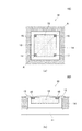
図1は、本発明の第一の実施形態による半導体装置100を説明するための図であり、図1(a)は、平面図、図1(b)は、図1(a)のA−A線に沿った断面図である。
Hereinafter, embodiments for carrying out the present invention will be described with reference to the drawings.
1A and 1B are diagrams for explaining a
図1に示すように本実施形態の半導体装置100は、P型(第一導電型)の半導体基板11と、半導体基板11上に設けられたホール素子10と、ホール素子10の周囲を取り囲むように設けられたP型の素子分離拡散層14とを備えている。
As shown in FIG. 1, the
ホール素子10は、半導体基板11上に半導体基板11と離間して設けられたN型(第二導電型)の磁気感受部12と、半導体基板11上において、磁気感受部12の側面および底面を囲むように設けられ、磁気感受部12より低濃度かつ濃度分布が一定のN型の半導体層13と、磁気感受部12の表面に設けられた磁気感受部12より高濃度のN型不純物層からなる電極15〜18とを備えている。
The
また、磁気感受部12および半導体層13の表面の電極15〜18および素子分離拡散層14が設けられている領域を除く領域を覆うように、絶縁膜(例えば、シリコン酸化膜)19が設けられている。これにより、磁気感受部12表面において、半導体基板11と平行に流れる電流を抑制することができる。
In addition, an insulating film (for example, a silicon oxide film) 19 is provided so as to cover a region excluding a region where the
かかる構成によれば、半導体基板11と半導体層13とのPN接合部に生じた空乏層は、半導体基板11側と半導体層13側の両方に広がり、半導体層13側に広がる空乏層は、磁気感受部12の方へ向かって広がる。しかし、半導体基板11と磁気感受部12とは直接接しておらず、半導体基板11と磁気感受部13の間には、半導体層が介在しており、かつ、磁気感受部12が半導体層13よりも高濃度であることから、空乏層が磁気感受部12まで到達することを防止することができる。
According to such a configuration, the depletion layer generated at the PN junction between the
さらに、半導体層13は、その濃度分布が一定であるため、半導体基板11との接合部のどの部分においても、形成される空乏層の広がり方が均一となる。したがって、磁気感受部12にまで空乏層が広がることを確実に抑制し、ホール素子の特性ばらつきを低減することができる。
Furthermore, since the concentration distribution of the
したがって、本実施形態のホール素子10において、スピニングカレント法によるオフセットキャンセルを行った場合に、電流を流す方向を切り替えても、各電流印加方向において生成される空乏層の広がり方をほぼ同等とすることができる。よって、オフセット電圧を十分に低減することが可能となる。
Therefore, in the
なお、N型不純物の濃度分布が一定である半導体層13は、例えば、半導体基板11上にエピタキシャル成長することにより形成される。そして、磁気感受部12は、例えば、エピタキシャル成長により形成した半導体層13にN型の不純物を導入することにより形成される。
The
ここで、一般に、ホール素子の磁気感度は、移動度に比例して高くなることが知られていることから、磁気感受部12の不純物濃度は低いほど好ましく、例えば、1×10¹⁶〜1×10¹⁸atoms/cm3程度であることが好ましい。また、エピタキシャル成長によって形成される半導体層13の不純物濃度は、半導体基板11と半導体層13とのPN接合部に形成される空乏層が磁気感受部12に達することが確実に抑制されるように、磁気感受部12よりも低い濃度に設定する必要がある。そのため、例えば、1×1015〜1×1016atoms/cm3程度であることが好ましい。
Here, since it is generally known that the magnetic sensitivity of the Hall element increases in proportion to the mobility, the impurity concentration of the
また、深さ(厚さ)方向に関しても、半導体基板11と半導体層13とのPN接合部に形成される空乏層が磁気感受部12に到達しないようにするため、それぞれの厚さを適宜設定する必要があり、例えば、磁気感受部12の深さ(厚さ)を3〜5μm程度とした場合、半導体層13の深さ(厚さ)を6〜9μm程度とすることが好ましい。
Also, with respect to the depth (thickness) direction, each thickness is appropriately set to prevent a depletion layer formed at the PN junction between the
素子分離拡散層14は、半導体層13の底よりも深く、半導体基板11に達するように形成されている。これにより、ホール素子10を半導体基板11上の他の領域(図示せず)に形成されるホール素子10からの信号を処理する回路等を構成する素子、例えば、MOSトランジスタ等から電気的に分離している。このように、図示せぬ領域にMOSトランジスタ等を設ける場合、これを形成するためのウェルとホール素子10を構成する磁気感受部12とは同じ工程によって形成することができる。したがって、製造工程数の増加を抑制することができる。
The element
本実施形態による半導体装置100では、PN接合を構成するP型の半導体基板11とN型の半導体層13とは、いずれも濃度が低いため、高温になると接合リークが生じやすくなる。接合リークが生じると、本来流れるべき磁気感受部12以外へ電流が流れてしまうことになる。そのため、感度が低下したり、スピニングカレント法によるオフセットキャンセルを行った場合に、電流を流す方向を切り替えた際の各電流印加方向でのリーク電流にばらつきが生じることから、オフセット電圧を除去しきれなくなる場合が生じる。
In the
そこで、本発明の第二〜第四の実施形態として、第一の実施形態の半導体装置100において得られる上記効果を維持しつつ、さらに高温時の接合リークを低減する構成につき、以下に説明する。
Accordingly, as second to fourth embodiments of the present invention, configurations that reduce junction leakage at high temperatures while maintaining the above-described effects obtained in the
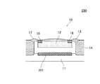
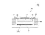
図2〜4は、本発明の第二〜第四の実施形態による半導体装置200〜400をそれぞれ説明するための断面図である。各断面図については、図1(a)の平面図に対応しているため、図示を省略する。
なお、図1に示す半導体装置100と同一の構成要素には同一の符号を付し、重複する説明は適宜省略する。
2 to 4 are cross-sectional views for explaining the
Note that the same components as those of the
第二の実施形態による半導体装置200は、図2に示すように、第一の実施形態による半導体装置100に対し、ホール素子10の下部において、P型の半導体基板11とN型の半導体膜13との間にP型の埋込層201をさらに備えている。
As shown in FIG. 2, the
このP型の埋込層201の濃度は、P型の半導体基板11よりも高くなっている。
このように、半導体基板11よりも高濃度のP型の埋込層201を設けることにより、ホール素子10の下部に形成されるPN接合は、半導体基板11と半導体層13との間ではなく、P型の埋込層201とN型の半導体層13との間に形成される。
The concentration of the P type buried
Thus, by providing the P type buried
PN接合におけるリーク電流は、少なくとも一方を高濃度にすることにより低減することができる。したがって、上記構成によれば、PN接合を形成する埋込層201と半導体層13の一方である埋込層201が高濃度であるため、第一の実施形態による半導体装置100と比べ、接合リークを低減することが可能となる。よって、スピニングカレント法によるオフセットキャンセルを行った場合、オフセット電圧を十分に低減することが可能となる。
The leakage current in the PN junction can be reduced by increasing the concentration of at least one of them. Therefore, according to the above configuration, since the buried
ただし、半導体層13が半導体基板11とではなく高濃度の埋込層201と接合することになるため、第一の実施形態による半導体装置100における空乏層よりも、半導体層13側への空乏層の広がりが大きくなる。したがって、本実施形態では、空乏層が磁気感受部12へ到達しないように、半導体層13の深さ(厚さ)や濃度、および埋込層201の厚さや濃度を適宜調節し、最適化する必要がある。
ここで、埋込層201は、例えば、半導体基板11の表面からP型不純物を導入し、その後、エピタキシャル成長により半導体層13を形成することにより形成される。
However, since the
Here, the buried
次に、第三の実施形態による半導体装置300は、図3に示すように、第一の実施形態による半導体装置100に対し、ホール素子10の下部において、P型の半導体基板11とN型の半導体膜13との間にN型の埋込層301を備えている。
Next, as shown in FIG. 3, the
このN型の埋込層301の濃度は、N型の半導体膜13よりも高くなっている。
このように、半導体膜13よりも高濃度のN型の埋込層301を設けることにより、ホール素子10の下部に形成されるPN接合は、半導体基板11と半導体層13との間ではなく、P型の半導体基板11とN型の埋込層301との間に形成される。
The concentration of the N-type buried
Thus, by providing the N type buried
かかる構成によれば、PN接合を形成する半導体基板11と埋込層301の一方である埋込層301が高濃度であるため、第二の実施形態による半導体装置200と同様、第一の実施形態による半導体装置100と比べ、接合リークを低減することが可能となる。
According to such a configuration, since the buried
さらに、本実施形態によれば、半導体基板11と埋込層301とのPN接合部に形成される空乏層は、N型の埋込層301の濃度が高いことから、半導体層13側に広がる空乏層は、埋込層301内に収まるか、埋込層301よりも広がった場合でも半導体層13内に少しかかる程度となる。したがって、半導体層13の厚さを薄くしても、空乏層が磁気感受部12に達することを防止することができる。よって、半導体層13をエピタキシャル成長により形成する場合には、その厚さを薄くできることから、製造コストを低減することも可能となる。
Furthermore, according to the present embodiment, the depletion layer formed at the PN junction between the
ただし、N型の埋込層301の濃度を高くし過ぎてしまうと、電極15、16間の磁気感受部12内を流れるはずの電流が抵抗の低い埋込層301へ流れやすくなってしまう。そのため、半導体層13の深さ(厚さ)や濃度、および埋込層301の厚さや濃度を適宜調節し、最適化する必要がある。
ここで、埋込層301は、例えば、半導体基板11の表面からN型不純物を導入し、その後、エピタキシャル成長により半導体層13を形成することにより形成される。
However, if the concentration of the N-type buried
Here, the buried
次に、第四の実施形態による半導体装置400は、図4に示すように、第一の実施形態による半導体装置100に対し、ホール素子10の下部において、P型の半導体基板11とN型の半導体膜13との間に埋込層401を備えている。
Next, as shown in FIG. 4, the
埋込層401は、半導体基板11側に設けられたP型の埋込層402と、埋込層402の上面に接するように半導体層13側に設けられたN型の埋込層403とを含んで構成されている。
P型の埋込層402は、P型の半導体基板11よりも高濃度であり、N型の埋込層403は、N型の半導体層13よりも高濃度である。
The buried
The P type buried
このように、本実施形態においては、ホール素子10の下部に形成されるPN接合は、半導体基板11と半導体層13との間ではなく、P型の埋込層402とN型の埋込層403との間に形成される。
Thus, in the present embodiment, the PN junction formed below the
かかる構成によれば、PN接合を形成するP型の埋込層402とN型の埋込層403がいずれも高濃度であるため、第二および第三の実施形態による半導体装置200および300よりもさらに接合リークを低減することが可能となる。
According to such a configuration, since both the P-type buried
さらに、本実施形態によれば、P型の埋込層402とN型の埋込層403とのPN接合部に形成される空乏層は、埋込層402および埋込層403がいずれも高濃度であることから、半導体基板11側に広がる空乏層も、半導体層13側に広がる空乏層も狭くなる。したがって、半導体層13側に広がる空乏層は、第三の実施形態による半導体装置300と同様、埋込層301内に収まるか、埋込層301よりも広がった場合でも半導体層13内に少しかかる程度となる。したがって、半導体層13の厚さを薄くしても、空乏層が磁気感受部12に達することを防止することができる。よって、半導体層13をエピタキシャル成長により形成する場合には、その厚さを薄くできることから、本実施形態においても、製造コストを低減することも可能となる。
Further, according to the present embodiment, the depletion layer formed at the PN junction between the P-type buried
ただし、第三の実施形態による半導体装置300と同様、N型の埋込層403の濃度を高くし過ぎてしまうと、電極15、16間の磁気感受部12内を流れるはずの電流が抵抗の低い埋込層403へ流れやすくなってしまう。そのため、半導体層13の深さ(厚さ)や濃度、および埋込層403の厚さや濃度を適宜調節し、最適化する必要がある。
However, as in the
ここで、埋込層401は、例えば、半導体基板11の表面からP型不純物を少し深めに導入し、さらに、N型不純物をP型不純物よりも浅めに導入し、その後、エピタキシャル成長により半導体層13を形成することにより形成される。
Here, for example, the buried
なお、埋込層402および403は、P型の埋込層402を半導体基板11側、N型の埋込層403を半導体層13側に形成する、すなわち、半導体基板11と同一導電型の埋込層を半導体基板11側に、半導体層13と同一導電型の埋込層を半導体層13側に形成する必要のが望ましい。N型の埋込層403をP型の半導体基板11側、P型の埋込層402をN型の半導体層13側に配置した場合でも、接合リークの低減にはつながる。しかし、このように配置してしまうと、埋込層403と半導体基板11とのPN接合部、および埋込層402と半導体層13とのPN接合部のそれぞれに空乏層が形成され、特に、P型の埋込層402とN型の半導体層13との間に形成される空乏層は、濃度の薄い半導体層13側へ大きく広がり、磁気感受部12へ影響を与え易くなってしまう。
The buried layers 402 and 403 are formed by forming the P type buried
以上、本発明の実施形態について説明したが、本発明は上記実施形態に限定されず、本発明の趣旨を逸脱しない範囲において種々の変更が可能であることは言うまでもない。
例えば、上記実施形態においては、第一導電型をP型、第二導電型をN型として説明したが、導電型を入れ替えて、第一導電型をN型、第二導電型をP型としても構わない。
As mentioned above, although embodiment of this invention was described, it cannot be overemphasized that this invention is not limited to the said embodiment, A various change is possible in the range which does not deviate from the meaning of this invention.
For example, in the above embodiment, the first conductivity type has been described as P-type and the second conductivity type has been described as N-type. However, the first conductivity type is changed to N-type and the second conductivity type is changed to P-type. It doesn't matter.
10 ホール素子
11 P型半導体基板
12 N型磁気感受部
13 N型半導体層
14 素子分離拡散層
15、16、17、18 電極
100、200、300、400 半導体装置
201、402 P型埋込層
301、403 N型埋込層
401 埋込層
DESCRIPTION OF
Claims (5)
前記半導体基板上に設けられたホール素子とを有する半導体装置であって、
前記ホール素子は、
前記半導体基板上に前記半導体基板と離間して設けられた第二導電型の磁気感受部と、
前記半導体基板上において、前記磁気感受部の側面および底面を囲むように設けられ、前記磁気感受部より低濃度かつ濃度分布が一定の第二導電型の半導体層とを備えることを特徴とする半導体装置。 A first conductivity type semiconductor substrate;
A semiconductor device having a Hall element provided on the semiconductor substrate,
The Hall element is
A magnetic sensing part of a second conductivity type provided on the semiconductor substrate apart from the semiconductor substrate;
A semiconductor comprising: a second conductive type semiconductor layer provided on the semiconductor substrate so as to surround a side surface and a bottom surface of the magnetic sensing portion and having a lower concentration and a constant concentration distribution than the magnetic sensing portion. apparatus.
前記埋込層は、
前記半導体基板側に設けられ、前記半導体基板よりも高濃度の第一導電型の第一の埋込層と、
前記第一の埋込層の上面に接するように前記半導体層側に設けられ、前記半導体層よりも高濃度の第二導電型の第二の埋込層とを含むことを特徴とする請求項1に記載の半導体装置。 In the lower part of the magnetic sensing part, further comprising a buried layer provided between the semiconductor substrate and the semiconductor layer,
The buried layer is
A first buried layer of a first conductivity type provided on the semiconductor substrate side and having a higher concentration than the semiconductor substrate;
The second embedded layer of the second conductivity type, which is provided on the semiconductor layer side so as to be in contact with the upper surface of the first embedded layer and has a higher concentration than the semiconductor layer. 2. The semiconductor device according to 1.
Priority Applications (5)
| Application Number | Priority Date | Filing Date | Title |
|---|---|---|---|
| JP2017090394A JP2018190793A (en) | 2017-04-28 | 2017-04-28 | Semiconductor device |
| TW107112480A TW201840023A (en) | 2017-04-28 | 2018-04-12 | Semiconductor device |
| KR1020180045454A KR20180121369A (en) | 2017-04-28 | 2018-04-19 | Semiconductor device |
| CN201810393464.1A CN108807659A (en) | 2017-04-28 | 2018-04-27 | Semiconductor device |
| US15/964,923 US20180315919A1 (en) | 2017-04-28 | 2018-04-27 | Semiconductor device |
Applications Claiming Priority (1)
| Application Number | Priority Date | Filing Date | Title |
|---|---|---|---|
| JP2017090394A JP2018190793A (en) | 2017-04-28 | 2017-04-28 | Semiconductor device |
Publications (2)
| Publication Number | Publication Date |
|---|---|
| JP2018190793A true JP2018190793A (en) | 2018-11-29 |
| JP2018190793A5 JP2018190793A5 (en) | 2020-05-28 |
Family
ID=63916183
Family Applications (1)
| Application Number | Title | Priority Date | Filing Date |
|---|---|---|---|
| JP2017090394A Pending JP2018190793A (en) | 2017-04-28 | 2017-04-28 | Semiconductor device |
Country Status (5)
| Country | Link |
|---|---|
| US (1) | US20180315919A1 (en) |
| JP (1) | JP2018190793A (en) |
| KR (1) | KR20180121369A (en) |
| CN (1) | CN108807659A (en) |
| TW (1) | TW201840023A (en) |
Families Citing this family (3)
| Publication number | Priority date | Publication date | Assignee | Title |
|---|---|---|---|---|
| US10333056B2 (en) * | 2017-07-27 | 2019-06-25 | Globalfoundries Singapore Pte. Ltd. | Hall element for 3-D sensing and method for producing the same |
| JP7266386B2 (en) * | 2018-11-09 | 2023-04-28 | エイブリック株式会社 | semiconductor equipment |
| CN116113309B (en) * | 2023-04-13 | 2023-07-25 | 南京邮电大学 | Low-offset Hall device adopting double protection rings and application method thereof |
Citations (3)
| Publication number | Priority date | Publication date | Assignee | Title |
|---|---|---|---|---|
| JP2005333103A (en) * | 2004-03-30 | 2005-12-02 | Denso Corp | Vertical hall device and manufacturing method of the same |
| WO2006085503A1 (en) * | 2005-02-08 | 2006-08-17 | Rohm Co., Ltd. | Magnetic sensor circuit and portable terminal provided with such magnetic sensor circuit |
| JP2016152271A (en) * | 2015-02-16 | 2016-08-22 | エスアイアイ・セミコンダクタ株式会社 | Method for manufacturing vertical hall element |
Family Cites Families (8)
| Publication number | Priority date | Publication date | Assignee | Title |
|---|---|---|---|---|
| CH668146A5 (en) * | 1985-05-22 | 1988-11-30 | Landis & Gyr Ag | FURNISHING WITH A HALL ELEMENT IN INTEGRATED SEMICONDUCTOR TECHNOLOGY. |
| JP4940965B2 (en) * | 2007-01-29 | 2012-05-30 | 株式会社デンソー | Rotation sensor and rotation sensor device |
| EP2234185B1 (en) * | 2009-03-24 | 2012-10-10 | austriamicrosystems AG | Vertical Hall sensor and method of producing a vertical Hall sensor |
| JP5815986B2 (en) * | 2010-07-05 | 2015-11-17 | セイコーインスツル株式会社 | Hall sensor |
| US9217783B2 (en) * | 2012-09-13 | 2015-12-22 | Infineon Technologies Ag | Hall effect device |
| KR102116147B1 (en) * | 2014-03-06 | 2020-05-28 | 매그나칩 반도체 유한회사 | Buried Magnetic Sensor |
| DE102015204637A1 (en) * | 2015-03-13 | 2016-09-15 | Infineon Technologies Ag | A method of doping an active Hall effect region of a Hall effect device and Hall effect device with a doped active Hall effect region |
| US10109787B2 (en) * | 2016-10-27 | 2018-10-23 | Texas Instruments Incorporated | Well-based vertical hall element with enhanced magnetic sensitivity |
-
2017
- 2017-04-28 JP JP2017090394A patent/JP2018190793A/en active Pending
-
2018
- 2018-04-12 TW TW107112480A patent/TW201840023A/en unknown
- 2018-04-19 KR KR1020180045454A patent/KR20180121369A/en unknown
- 2018-04-27 CN CN201810393464.1A patent/CN108807659A/en not_active Withdrawn
- 2018-04-27 US US15/964,923 patent/US20180315919A1/en not_active Abandoned
Patent Citations (3)
| Publication number | Priority date | Publication date | Assignee | Title |
|---|---|---|---|---|
| JP2005333103A (en) * | 2004-03-30 | 2005-12-02 | Denso Corp | Vertical hall device and manufacturing method of the same |
| WO2006085503A1 (en) * | 2005-02-08 | 2006-08-17 | Rohm Co., Ltd. | Magnetic sensor circuit and portable terminal provided with such magnetic sensor circuit |
| JP2016152271A (en) * | 2015-02-16 | 2016-08-22 | エスアイアイ・セミコンダクタ株式会社 | Method for manufacturing vertical hall element |
Also Published As
| Publication number | Publication date |
|---|---|
| US20180315919A1 (en) | 2018-11-01 |
| TW201840023A (en) | 2018-11-01 |
| CN108807659A (en) | 2018-11-13 |
| KR20180121369A (en) | 2018-11-07 |
Similar Documents
| Publication | Publication Date | Title |
|---|---|---|
| JP6132032B2 (en) | Semiconductor device and manufacturing method thereof | |
| CN105633274B (en) | Vertical Hall element | |
| JP2018190793A (en) | Semiconductor device | |
| JP2017174863A (en) | Semiconductor device | |
| JP2014067986A (en) | Semiconductor device | |
| TW201735187A (en) | Semiconductor device | |
| KR20160063262A (en) | Vertical hall element | |
| US10263176B2 (en) | Semiconductor device having vertical hall element | |
| JP2018117036A (en) | Semiconductor device | |
| US10998492B2 (en) | Semiconductor device | |
| JP5271694B2 (en) | diode | |
| CN110945633A (en) | Semiconductor device with a plurality of semiconductor chips | |
| KR20200067234A (en) | Semiconductor device | |
| JP2019201097A (en) | Semiconductor device | |
| JP2011082505A (en) | Ac 4-terminal jfet geometric structure for reducing gate-to-source capacitance | |
| JP6001309B2 (en) | Semiconductor device | |
| TWI772556B (en) | Transient voltage suppression device, transient voltage suppression device assembly and methods for formation thereof | |
| JP2018206934A (en) | Silicon carbide semiconductor device and manufacturing method thereof | |
| TW202306206A (en) | Semiconductor device and manufacturing method thereof | |
| JP2016162898A (en) | Semiconductor device | |
| JP5069776B2 (en) | Magnetic detector | |
| JP2016134480A (en) | Semiconductor device | |
| JP6099956B2 (en) | Semiconductor device | |
| JP2020092208A (en) | Manufacturing method of trench gate type semiconductor device | |
| JP2018074106A (en) | Semiconductor element manufacturing method and chip having semiconductor element |
Legal Events
| Date | Code | Title | Description |
|---|---|---|---|
| A521 | Request for written amendment filed |
Free format text: JAPANESE INTERMEDIATE CODE: A523 Effective date: 20200415 |
|
| A621 | Written request for application examination |
Free format text: JAPANESE INTERMEDIATE CODE: A621 Effective date: 20200415 |
|
| A977 | Report on retrieval |
Free format text: JAPANESE INTERMEDIATE CODE: A971007 Effective date: 20210226 |
|
| A131 | Notification of reasons for refusal |
Free format text: JAPANESE INTERMEDIATE CODE: A131 Effective date: 20210303 |
|
| A02 | Decision of refusal |
Free format text: JAPANESE INTERMEDIATE CODE: A02 Effective date: 20211005 |