JP2018009874A - Magnetic probe - Google Patents
Magnetic probe Download PDFInfo
- Publication number
- JP2018009874A JP2018009874A JP2016138771A JP2016138771A JP2018009874A JP 2018009874 A JP2018009874 A JP 2018009874A JP 2016138771 A JP2016138771 A JP 2016138771A JP 2016138771 A JP2016138771 A JP 2016138771A JP 2018009874 A JP2018009874 A JP 2018009874A
- Authority
- JP
- Japan
- Prior art keywords
- magnetic
- sensor
- magnetic sensor
- flexible substrate
- flaw detection
- Prior art date
- Legal status (The legal status is an assumption and is not a legal conclusion. Google has not performed a legal analysis and makes no representation as to the accuracy of the status listed.)
- Pending
Links
Images


Landscapes
- Investigating Or Analyzing Materials By The Use Of Magnetic Means (AREA)
Abstract
【課題】柔軟性を有する基材に対する磁気センサの接合強度を高めることができる磁気探触子を提供する。
【解決手段】磁気探触子4は、1または複数の磁気センサ12と、磁気センサ12が取り付けられる柔軟性を有する基材10aと、磁気センサ12のそれぞれと基材10aとの間に設けられる複数の導通部40と、磁気センサ12のそれぞれと基材10aとの間に設けられ、少なくとも導通部40の周囲の領域を封止するアンダーフィル部43と、を備える。
【選択図】図3A magnetic probe capable of increasing the bonding strength of a magnetic sensor to a flexible substrate is provided.
A magnetic probe 4 is provided between one or a plurality of magnetic sensors 12, a flexible base material 10a to which the magnetic sensor 12 is attached, and each of the magnetic sensors 12 and the base material 10a. A plurality of conduction portions 40 and an underfill portion 43 provided between each of the magnetic sensors 12 and the base material 10 a and sealing at least a region around the conduction portion 40 are provided.
[Selection] Figure 3
Description
本発明は、磁気探触子に関する。 The present invention relates to a magnetic probe.
従来、対象物の表層のきず(JIS Z 2300:2009)を検出するための磁気を利用した非破壊検査として、漏洩磁束探傷法(Magnetic Flux Leakage:MFL)や渦電流探傷法(Eddy Current Testing:ECT)等が知られている。漏洩磁束探傷法は、対象物の探傷面を磁化し、きずから漏洩する磁束の有無等を磁気センサにより測定する方法である。また、渦電流探傷法は、対象物の表層に渦電流を発生させ、その電流が発生する磁界を磁気センサにより測定する方法である。 Conventionally, as non-destructive inspection using magnetism for detecting flaws on the surface of an object (JIS Z 2300: 2009), magnetic flux testing (Magnetic Flux Leakage: MFL) and eddy current testing (Eddy Current Testing: ECT) and the like are known. The leakage magnetic flux flaw detection method is a method in which a flaw detection surface of an object is magnetized and the presence or absence of magnetic flux leaking from a flaw is measured by a magnetic sensor. The eddy current flaw detection method is a method in which an eddy current is generated on the surface layer of an object, and a magnetic field generated by the current is measured by a magnetic sensor.
特許文献1には、磁気センサとして、SQUID(Superconducting QUantum Interference Device)センサを用いた非破壊検査装置が記載されている。SQUIDセンサは、底板に実装されている。SQUIDセンサは、底板に設けられた配線パターンに対して、超電導バンプにより接続されている。 Patent Document 1 describes a nondestructive inspection apparatus using a SQUID (Superconducting Quantum Interference Device) sensor as a magnetic sensor. The SQUID sensor is mounted on the bottom plate. The SQUID sensor is connected to the wiring pattern provided on the bottom plate by superconducting bumps.
バンプ接合は、磁気センサに対して、導通部のみにおいて設けられる。たとえば、平板状に延在する磁気センサにおいて、磁気センサの四隅のみがバンプ接合され得る。磁気センサが非常に小さい場合、または、接合領域が非常に小さい場合には、接合強度が不足する場合がある。特に、フレキシブル基板等の柔軟性を有する基板が用いられる場合には、フレキシブル基板が湾曲した際に磁気センサが剥離してしまう虞がある。 Bump bonding is provided only at the conduction portion with respect to the magnetic sensor. For example, in a magnetic sensor extending in a flat plate shape, only four corners of the magnetic sensor can be bump-bonded. If the magnetic sensor is very small, or if the bonding area is very small, the bonding strength may be insufficient. In particular, when a flexible substrate such as a flexible substrate is used, the magnetic sensor may peel off when the flexible substrate is curved.
本発明は、柔軟性を有する基材に対する磁気センサの接合強度を高めることができる磁気探触子を提供することを目的とする。 An object of this invention is to provide the magnetic probe which can raise the joint strength of the magnetic sensor with respect to the base material which has a softness | flexibility.
本発明の一態様に係る磁気探触子は、1または複数の磁気センサと、磁気センサが取り付けられる柔軟性を有する基材と、磁気センサのそれぞれと基材との間に設けられる複数の導通部と、磁気センサのそれぞれと基材との間に設けられ、少なくとも導通部の周囲の領域を封止するアンダーフィル部と、を備える。 A magnetic probe according to one embodiment of the present invention includes one or a plurality of magnetic sensors, a flexible base material to which the magnetic sensors are attached, and a plurality of electrical connections provided between each of the magnetic sensors and the base material. And an underfill portion that is provided between each of the magnetic sensors and the base material and seals at least a region around the conductive portion.
この磁気探触子によれば、磁気センサは、導通部のみならず、導通部の周囲の領域を封止するアンダーフィル部によって基材に対して接合されている。基材は柔軟性を有するが、基材が変形した場合でも、アンダーフィル部による補強効果によって、磁気センサの剥離や破損等が防止される。このように、アンダーフィル部によって、柔軟性を有する基材に対する磁気センサの接合強度が高められている。 According to this magnetic probe, the magnetic sensor is bonded to the base material by the underfill part that seals not only the conduction part but also the area around the conduction part. Although the base material has flexibility, even when the base material is deformed, peeling or breakage of the magnetic sensor is prevented by the reinforcing effect by the underfill portion. Thus, the bonding strength of the magnetic sensor to the flexible substrate is increased by the underfill portion.
いくつかの態様において、アンダーフィル部は、基材に対面する磁気センサの表面の全面に密着している。この場合、アンダーフィル部による補強効果が高められ、磁気センサがより確実に接合される。
In some embodiments, the underfill portion is in close contact with the entire surface of the magnetic sensor facing the substrate. In this case, the reinforcing effect by the underfill portion is enhanced, and the magnetic sensor is more reliably joined.
いくつかの態様において、磁気探触子は、対象物の探傷面上を磁気センサが走査することにより探傷面を含む表層のきずを探傷する漏洩磁束探傷装置に用いられる。漏洩磁束探傷装置において、柔軟性を有する基材を用いた場合、磁気探触子は、基材を変形させながら凹部や狭隘部等に挿入され得る。その場合でも、アンダーフィル部による補強効果によって、磁気センサの剥離や破損等が防止される。 In some embodiments, the magnetic probe is used in a leakage magnetic flux flaw detector that flaws a surface layer including a flaw detection surface by a magnetic sensor scanning over the flaw detection surface of the object. When a flexible base material is used in the leakage magnetic flux flaw detector, the magnetic probe can be inserted into a recess, a narrow part or the like while deforming the base material. Even in that case, peeling or breakage of the magnetic sensor is prevented by the reinforcing effect of the underfill portion.
本発明のいくつかの態様によれば、アンダーフィル部によって、柔軟性を有する基材に対する磁気センサの接合強度が高められる。 According to some aspects of the present invention, the underfill portion increases the bonding strength of the magnetic sensor to the flexible substrate.
以下、本発明の実施形態について、図面を参照しながら説明する。なお、図面の説明において同一要素には同一符号を付し、重複する説明は省略する。 Hereinafter, embodiments of the present invention will be described with reference to the drawings. In the description of the drawings, the same elements are denoted by the same reference numerals, and redundant descriptions are omitted.
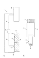
図1(A)に示されるように、漏洩磁束探傷装置1は、磁気探触子4を用いて検査対象である対象物Oの探傷面Eを走査し、探傷面Eを含む表層のきずXを探傷するための装置である。対象物Oは、たとえば航空機のジェットエンジンのシャフト等であるが、これに限られない。対象物Oは、磁性体であれば何であってもよい。
As shown in FIG. 1 (A), the magnetic flux leakage flaw detector 1 scans the flaw detection surface E of the object O to be inspected using the
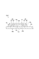
漏洩磁束探傷法の原理について説明する。漏洩磁束探傷法とは、図2(A)に示されるように、強磁性体からなる対象物Oの表面を含む表層に存在し得るきずXを、磁気センサTを用いて探索する検査法である。図2(B)に示されるように、漏洩磁束探傷法では、種々の方法により対象物Oを磁化することにより、対象物Oに所定方向の磁束Fを発生させる。磁束Fを遮るきずXがある場合には、そのきずXに起因して漏洩磁束Faが発生する。対象物Oの探傷面E上で磁気センサTを走査方向Dに走査させることにより、漏洩磁束Faが検出される。磁気センサTからの信号を用いる漏洩磁束探傷法は、従来採用されてきた磁粉探傷法に比して、探傷の自動化と結果のデジタル化とが容易であるという利点を有する。 The principle of the leakage magnetic flux flaw detection method will be described. As shown in FIG. 2 (A), the leakage magnetic flux flaw detection method is an inspection method that uses a magnetic sensor T to search for flaws X that may exist on the surface layer including the surface of the object O made of a ferromagnetic material. is there. As shown in FIG. 2B, in the leakage magnetic flux flaw detection method, a magnetic flux F in a predetermined direction is generated on the object O by magnetizing the object O by various methods. When there is a flaw X that blocks the magnetic flux F, a leakage magnetic flux Fa is generated due to the flaw X. By causing the magnetic sensor T to scan in the scanning direction D on the flaw detection surface E of the object O, the leakage magnetic flux Fa is detected. The leakage magnetic flux flaw detection method using a signal from the magnetic sensor T has an advantage that the flaw detection automation and the digitization of the result are easier than the magnetic particle flaw detection method conventionally employed.
図1(A)に示されるように、漏洩磁束探傷装置1は、対象物Oの探傷面Eを走査するための磁気探触子4と、磁気探触子4からの信号を入力して所定の処理を行い、探傷試験の結果を出力するパーソナルコンピュータ(処理部。以下、PCという)20とを備える。磁気探触子4には複数のリード線14が設けられており、これらのリード線14が、たとえばAD変換器15に接続される。AD変換器15とPC20とは、USBケーブル等のケーブル16によって接続される。磁気探触子4は、走査方向Dに走査させられる。この走査は、手動で行われてもよく、自動で行われてもよい。磁気探触子4を保持するアーム等が走査方向Dに移動することで走査が行われてもよいし、磁気探触子4を固定した状態で、対象物Oを保持したステージ等が走査方向Dと逆方向に移動することで走査が行われてもよい。
As shown in FIG. 1 (A), the leakage magnetic flux flaw detector 1 receives a
図1(B)に示されるように、磁気探触子4は、計装アンプ基板11と、計装アンプ基板11に取り付けられたセンサモジュール10とを含む。計装アンプ基板11は、磁気探触子4から出力される信号を増幅させる。センサモジュール10は、フレキシブル基板(基材)10aと、フレキシブル基板10aに搭載された複数の磁気センサ12(図2(B)に示される磁気センサTに相当)と、を含む。フレキシブル基板10aは、計装アンプ基板11に対して差し込まれ、コネクタ接続されている。磁気探触子4において、センサモジュール10のみを交換することが可能になっている。漏洩磁束探傷装置1は、磁気探触子4の位置情報を取得するためのエンコーダ13を備えており、エンコーダ13のワイヤの端部がフレキシブル基板10aに連結されている。
As shown in FIG. 1B, the
PC20は、磁気探触子4から出力される、磁束に基づく磁界を示す信号と、エンコーダ13から出力される磁気探触子4の位置情報とを入力し、対象物Oの探傷面(表面)Eを含む表層におけるきずXの有無判定のための探傷試験結果を出力する。きずXが存在する場合には、探傷試験結果において、きず指示が表れる。探傷試験結果に表れるきず指示に基づいて、きずXの有無だけでなく、きずXの幅や長さを推定することも可能である。
The
以下、図3〜図5を参照して、一実施形態に係る磁気探触子4について詳細に説明する。漏洩磁束探傷装置1の磁気探触子4は、対象物Oに当接して湾曲した場合でも、フレキシブル基板10aに対する磁気センサ12の剥離や破損等を防止し得る構造を有している。磁気探触子4のセンサモジュール10は、柔軟性を有するフレキシブル基板10aを含む。フレキシブル基板10aは、主として高分子材料からなるシート状の基材である。フレキシブル基板10aには、配線パターンが形成されている。これらの配線パターンは、各磁気センサ12の電極部12c(図4参照)と、上記の計装アンプ基板11の回路とを電気的に接続する。計装アンプ基板11は、柔軟性を有しておらず、定形性を有する。すなわち、磁気探触子4では、柔軟性を有するフレキシブル基板10aからセンサ部が構成され、定形性を有する計装アンプ基板11から信号出力部が構成される。
Hereinafter, the
フレキシブル基板10aには、たとえば複数の磁気センサ12が取り付けられている。磁気センサ12は、探傷面Eの近傍において磁界の大きさを測定可能なセンサである。磁気センサ12は、磁界検出部(図示せず)を含む。磁気センサ12としては、MI(Magneto-Impedance)センサ、GMR(Giant Magneto Resistive effect)センサ、TMR(Tunnel Magneto-Resistance)センサ、AMR(Anisotropic Magneto-Resistance)センサ、FG(Flux-Gate)センサ、ホール素子、SQUID(Superconducting QUantum Interference Device)センサ、コイル等が用いられ得る。
For example, a plurality of
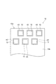
各磁気センサ12は、フレキシブル基板10aに搭載されている。磁気センサ12は、なお、磁気センサ12の個数は、特に限定されない。磁気センサ12の個数は、1個であってもよい。複数の磁気センサ12が設けられる場合、磁気センサ12は、一列に配列されてもよいし、複数列に配列されてもよい。磁気センサ12が複数列に配列される場合、複数の磁気センサ12が千鳥状に配置されてもよい(図5参照)。
Each
フレキシブル基板10aに実装される磁気センサ12としては、非常に小型の磁気センサが用いられ得る。磁気センサ12は、一辺の長さが1mm以下の磁気センサ(TMRセンサ等)であってもよい。磁気センサ12は、一辺の長さが2mm以下の磁気センサであってもよく、一辺の長さが4mm以下の磁気センサ(AMRセンサ等)であってもよい。
As the
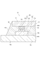
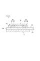
図3および図4に示されるように、磁気センサ12は、フレキシブル基板10aに対して平行に設けられ、フレキシブル基板10aに対面している。磁気センサ12の第2面12bが、フレキシブル基板10aの第1面10bに対面している。磁気センサ12とフレキシブル基板10aとの間には、複数の導通部40が設けられている。導通部40は、たとえば、磁気センサ12の電極部12cに対応して、矩形の磁気センサ12の4つの隅部に設けられている。
As shown in FIGS. 3 and 4, the
導通部40は、フレキシブル基板10aの第1面10bに設けられた電極パッド42と、電極パッド42と電極部12cとを接合する接合部41とを含む。電極パッド42は、たとえば、ニッケル(Ni)層と、パラジウム(Pd)層と、金(Au)層とを含む(いずれも図示せず)。接合部41は、図4に示されるように、電極部12cに当接するバンプ41aと、バンプ41aおよび電極パッド42を接合する半田部41bとを含む。バンプ41aは、たとえば金からなる。接合部41における接合は、超音波ボンディングによって行われてもよい。上記したように磁気センサ12は微小なセンサであるので、電極部12cおよび導通部40は、たとえば0.1mm程度の微小なサイズになり得る。超音波ボンディングによれば、微小な電極部12cに対しても接合強度を高めることができる。
The
さらに、センサモジュール10は、磁気センサ12とフレキシブル基板10aとの間に設けられたアンダーフィル部43を備える。アンダーフィル部43は、たとえばエポキシ系樹脂等の樹脂からなる。アンダーフィル部43は、超音波ボンディングによって導通部40を形成した後に、たとえば、磁気センサ12とフレキシブル基板10aとの間の間隙に樹脂材料を流し込み、特定の温度で所定時間加熱した後、更に温度を上げて所定時間加熱するといった手法によって形成される。アンダーフィル部43は、たとえば柔軟性を有する材料であってもよいが、柔軟性が低い硬質の材料であってもよい。硬質の材料を用いた場合は、センサモジュール10(磁気探触子4の)ロバスト性の向上を図ることができる。
Further, the
アンダーフィル部43の第1面43aは、導通部40を除く領域において、磁気センサ12の第2面12bの全面に密着する。アンダーフィル部43の第2面43bは、導通部40を除く領域において、フレキシブル基板10aの第1面10bに密着する。アンダーフィル部43は、磁気センサ12よりも一回り大きく形成されてもよい。言い換えれば、フレキシブル基板10aに対して、その第1面10bに垂直な方向に磁気センサ12とアンダーフィル部43を投影した場合に、アンダーフィル部43の投影領域は磁気センサ12の投影領域を含む。アンダーフィル部43は、磁気センサ12の側面を覆うと共に、磁気センサ12の外周から広がるように傾斜する側面部43cを含んでもよい。
The
アンダーフィル部43は、磁気センサ12とフレキシブル基板10aとの間であって、導通部40を除く領域のすべてに充填されてもよい。磁気センサ12とフレキシブル基板10aとの間の全域を封止するアンダーフィル部43によれば、磁気センサ12の接合強度が高められる。なお、磁気センサ12とフレキシブル基板10aとの間において、アンダーフィル部43が存在しない領域があってもよい。アンダーフィル部43は、少なくとも導通部40の周囲の領域を封止してもよい。
The
上記した探触子4を用いて走査が行われる際には、対象物Oが、公知の手段(ハンドマグナ等)によって磁化される。そして、センサモジュール10は、走査方向Dに移動させられる。磁気センサ12は、フレキシブル基板10aの対象物Oに対面する面(すなわち第2面10c)とは反対側(すなわち第1面10b側)に配置され得る。このような配置により、磁気センサ12が探傷面Eに当接することが防止され得る。
When scanning is performed using the
センサモジュール10において、第2面10cが対象物Oの探傷面Eに押し付けられる。この際、図6に示すように、柔軟性を有するフレキシブル基板10aは湾曲し得る。一方で、柔軟性を有さない磁気センサ12は、ほとんど湾曲しない。磁気センサ12とフレキシブル基板10aとの間に設けられたアンダーフィル部43は、磁気センサ12の接合強度を高めているので、フレキシブル基板10aが変形した場合でも、磁気センサ12の剥離が防止されている。
In the
なお、磁気センサ12は、対象物Oの探傷面Eに対面するように配置されてもよい。磁気センサ12の第1面12aは、対象物Oの探傷面Eに当接してもよい。磁気センサ12の第1面12a上に、磁束の測定に影響を与えない保護シートが設けられてもよい。その場合に、センサモジュール10が対象物Oの探傷面Eに押し付けられてフレキシブル基板10aが変形したとしても、アンダーフィル部43は、磁気センサ12の剥離を防止する。
The
センサモジュール10による走査の結果、探傷面Eの近傍における磁気センサ12が検出する磁界の大きさに応じた電気信号が、磁気センサ12からPC20に対して出力される。
As a result of scanning by the
本実施形態の磁気探触子4によれば、磁気センサ12は、導通部40のみならず、導通部40の周囲の領域を封止するアンダーフィル部43によってフレキシブル基板10aに対して接合されている。フレキシブル基板10aは柔軟性を有するが、フレキシブル基板10aが変形した場合でも、アンダーフィル部43による補強効果によって、磁気センサ12の剥離や破損等が防止される。このように、アンダーフィル部43によって、柔軟性を有するフレキシブル基板10aに対する磁気センサ12の接合強度が高められている。
According to the
アンダーフィル部がフレキシブル基板10aに対面する磁気センサ12の第2面12bの全面に密着しているので、アンダーフィル部43による補強効果が高められ、磁気センサ12がより確実に接合されている。
Since the underfill portion is in close contact with the entire surface of the
磁気探触子4は漏洩磁束探傷装置1に用いられる。漏洩磁束探傷装置1において、柔軟性を有するフレキシブル基板10aを用いた場合、磁気探触子4は、フレキシブル基板10aを変形させながら凹部や狭隘部等に挿入され得る。その場合でも、アンダーフィル部43による補強効果によって、磁気センサ12の剥離や破損等が防止される。
The
図7を参照して、他の実施形態に係る磁気探触子4Aのセンサモジュール10Aについて説明する。磁気探触子4Aは、漏洩磁束探傷法とは異なる手法を用いた探傷方法及び探傷装置に適用される。磁気を用いて対象物の表層の探傷を行う手法としては、上記実施形態で説明した漏洩磁束探傷方法のほかに、渦電流探傷法(Eddy Current Testing:ECT)が挙げられる。渦電流探傷法とは、交流の電流を流した励磁コイルによって探傷対象面に渦電流を誘起させると共に、きずに由来する渦電流の変化を磁気センサで検出する手法である。
With reference to FIG. 7, a
図7に示されるように、渦電流探傷装置に適用される磁気探触子4Aのセンサモジュール10Aは、フレキシブル基板10aの第2面10cに設けられた励磁コイルCを備える。励磁コイルCは、第2面10cに垂直な方向に投影された場合に、上記した磁気センサ12の磁界検出部よりも大きくなっている。励磁コイルCは、磁気センサ12が設けられた領域をカバーする大きさおよび位置に設けられている。このようなセンサモジュール10Aを備えた磁気探触子4Aによっても、上記実施形態と同様の作用・効果が奏される。
As shown in FIG. 7, the
以上、本発明の実施形態について説明したが、本発明は上記実施形態に限定されない。たとえば、基材はフレキシブル基板10aである場合に限られない。フレキシブル基板10a以外の柔軟性を有する基板が用いられてもよい。
As mentioned above, although embodiment of this invention was described, this invention is not limited to the said embodiment. For example, the base material is not limited to the
導通部40の接合部41において、バンプ接合が用いられなくてもよい。バンプ41aを用いずに、半田部41bのみとしてもよい。導通部40の構造は、公知のあらゆる手段が用いられ得る。
Bump bonding may not be used in the
1 漏洩磁束探傷装置
4 磁気探触子
4A 磁気探触子
10 センサモジュール
10A センサモジュール
10a フレキシブル基板(基材)
11 計装アンプ基板
12 磁気センサ
12a 第1面
12b 第2面(表面)
12c 電極部
20 PC
40 導通部
41 接合部
41a バンプ
41b 半田部
42 電極パッド
43 アンダーフィル部
D 走査方向
E 探傷面
F 磁束
Fa 漏洩磁束
O 対象物
T 磁気センサ
X きず
DESCRIPTION OF SYMBOLS 1 Leakage magnetic
11
40
Claims (3)
前記磁気センサが取り付けられる柔軟性を有する基材と、
前記磁気センサのそれぞれと前記基材との間に設けられる複数の導通部と、
前記磁気センサのそれぞれと前記基材との間に設けられ、少なくとも前記導通部の周囲の領域を封止するアンダーフィル部と、を備える、磁気探触子。 One or more magnetic sensors;
A flexible substrate to which the magnetic sensor is attached;
A plurality of conducting portions provided between each of the magnetic sensors and the base material;
A magnetic probe comprising: an underfill portion provided between each of the magnetic sensors and the base material and sealing at least a region around the conduction portion.
3. The magnetic probe according to claim 1, wherein the magnetic probe is used in a leakage magnetic flux flaw detector that detects flaws on a surface layer including a flaw detection surface by scanning a flaw detection surface of an object.
Priority Applications (1)
| Application Number | Priority Date | Filing Date | Title |
|---|---|---|---|
| JP2016138771A JP2018009874A (en) | 2016-07-13 | 2016-07-13 | Magnetic probe |
Applications Claiming Priority (1)
| Application Number | Priority Date | Filing Date | Title |
|---|---|---|---|
| JP2016138771A JP2018009874A (en) | 2016-07-13 | 2016-07-13 | Magnetic probe |
Publications (1)
| Publication Number | Publication Date |
|---|---|
| JP2018009874A true JP2018009874A (en) | 2018-01-18 |
Family
ID=60995379
Family Applications (1)
| Application Number | Title | Priority Date | Filing Date |
|---|---|---|---|
| JP2016138771A Pending JP2018009874A (en) | 2016-07-13 | 2016-07-13 | Magnetic probe |
Country Status (1)
| Country | Link |
|---|---|
| JP (1) | JP2018009874A (en) |
Cited By (1)
| Publication number | Priority date | Publication date | Assignee | Title |
|---|---|---|---|---|
| JP2020067416A (en) * | 2018-10-26 | 2020-04-30 | 株式会社Ihi | Creep remaining life diagnostic method and creep remaining life diagnostic system |
Citations (8)
| Publication number | Priority date | Publication date | Assignee | Title |
|---|---|---|---|---|
| JPS58153157A (en) * | 1982-03-05 | 1983-09-12 | Shimadzu Corp | Magnetic detector for magnetic flaw detector |
| JPH08101167A (en) * | 1994-09-30 | 1996-04-16 | Tokyo Gas Co Ltd | Nondestructive inspection sensor and manufacturing method thereof |
| JP2003107056A (en) * | 2001-09-28 | 2003-04-09 | Nippon Steel Corp | Magnetic field sensor module for detecting magnetic flux leakage |
| JP2003238935A (en) * | 2002-02-18 | 2003-08-27 | Sony Chem Corp | Adhesives and electrical equipment |
| JP2005112916A (en) * | 2003-10-03 | 2005-04-28 | Nitto Denko Corp | Underfill adhesive film and semiconductor device using the same |
| JP2006248232A (en) * | 2001-01-29 | 2006-09-21 | Ube Ind Ltd | COF flexible substrates and electronic components |
| US20090115411A1 (en) * | 2007-11-05 | 2009-05-07 | Haiyan Sun | Flexible eddy current array probe and methods of assembling the same |
| JP2016114533A (en) * | 2014-12-17 | 2016-06-23 | コニカミノルタ株式会社 | Pipe with magnetic sensor, and nondestructive inspection device |
-
2016
- 2016-07-13 JP JP2016138771A patent/JP2018009874A/en active Pending
Patent Citations (8)
| Publication number | Priority date | Publication date | Assignee | Title |
|---|---|---|---|---|
| JPS58153157A (en) * | 1982-03-05 | 1983-09-12 | Shimadzu Corp | Magnetic detector for magnetic flaw detector |
| JPH08101167A (en) * | 1994-09-30 | 1996-04-16 | Tokyo Gas Co Ltd | Nondestructive inspection sensor and manufacturing method thereof |
| JP2006248232A (en) * | 2001-01-29 | 2006-09-21 | Ube Ind Ltd | COF flexible substrates and electronic components |
| JP2003107056A (en) * | 2001-09-28 | 2003-04-09 | Nippon Steel Corp | Magnetic field sensor module for detecting magnetic flux leakage |
| JP2003238935A (en) * | 2002-02-18 | 2003-08-27 | Sony Chem Corp | Adhesives and electrical equipment |
| JP2005112916A (en) * | 2003-10-03 | 2005-04-28 | Nitto Denko Corp | Underfill adhesive film and semiconductor device using the same |
| US20090115411A1 (en) * | 2007-11-05 | 2009-05-07 | Haiyan Sun | Flexible eddy current array probe and methods of assembling the same |
| JP2016114533A (en) * | 2014-12-17 | 2016-06-23 | コニカミノルタ株式会社 | Pipe with magnetic sensor, and nondestructive inspection device |
Cited By (2)
| Publication number | Priority date | Publication date | Assignee | Title |
|---|---|---|---|---|
| JP2020067416A (en) * | 2018-10-26 | 2020-04-30 | 株式会社Ihi | Creep remaining life diagnostic method and creep remaining life diagnostic system |
| JP7215076B2 (en) | 2018-10-26 | 2023-01-31 | 株式会社Ihi | Creep Remaining Life Diagnosis Method and Creep Remaining Life Diagnosis System |
Similar Documents
| Publication | Publication Date | Title |
|---|---|---|
| US7952348B2 (en) | Flexible eddy current array probe and methods of assembling the same | |
| US9678175B2 (en) | Eddy current detection | |
| JP4776696B2 (en) | Method and apparatus for nondestructive evaluation of defects in metal objects | |
| US6954065B2 (en) | Eddy-current probe | |
| CN103487502B (en) | The eddy current array probe of detection of complex conductive structure surfaces defect and system | |
| US8717012B2 (en) | Eddy current probe for surface and sub-surface inspection | |
| CN104634867A (en) | Eddy current inspection for case hardening depth | |
| US10634645B2 (en) | Eddy current probe with 3-D excitation coils | |
| JP7351332B2 (en) | Eddy current flaw detection probe, flaw detection method, and eddy current flaw detection equipment | |
| US8723513B2 (en) | Eddy current probe for surface inspection and eddy current inspection device including the same | |
| JP2018009874A (en) | Magnetic probe | |
| JP3572452B2 (en) | Eddy current probe | |
| JP2019020273A (en) | Surface flaw inspection device | |
| US11499941B2 (en) | Eddy current probe | |
| Sergeeva-Chollet et al. | Eddy current probes based on magnetoresistive array sensors as receivers | |
| JP5229923B2 (en) | Non-destructive inspection device using SQUID magnetic sensor | |
| JP7073617B2 (en) | Detector, magnetic flux leakage detector, and magnetic flux leakage detection method | |
| Chomsuwan et al. | High-Spatial Resolution Giant Magnetoresistive Sensors-Part I: Application in Non-Destructive Evaluation | |
| Sun et al. | Enhanced flaw detection using an eddy current probe with a linear array of hall sensors | |
| JP4735075B2 (en) | Sensor for crack depth measuring instrument and crack depth measuring instrument | |
| CN116818882B (en) | Non-destructive testing sensors and non-destructive testing systems | |
| KR102487591B1 (en) | Flexible arrayed and current probe for non-destructive testing of welds | |
| JP2019020272A (en) | Front surface scratch inspection device | |
| Paul et al. | Microsystem Technology for Eddy Current Testing | |
| Yamada et al. | Metallic Bead Detection by Using Eddy‐Current Probe with SV‐GMR Sensor |
Legal Events
| Date | Code | Title | Description |
|---|---|---|---|
| A621 | Written request for application examination |
Free format text: JAPANESE INTERMEDIATE CODE: A621 Effective date: 20190530 |
|
| A977 | Report on retrieval |
Free format text: JAPANESE INTERMEDIATE CODE: A971007 Effective date: 20200515 |
|
| A131 | Notification of reasons for refusal |
Free format text: JAPANESE INTERMEDIATE CODE: A131 Effective date: 20200630 |
|
| A02 | Decision of refusal |
Free format text: JAPANESE INTERMEDIATE CODE: A02 Effective date: 20210105 |