JP2017508246A - LED lighting device - Google Patents
LED lighting device Download PDFInfo
- Publication number
- JP2017508246A JP2017508246A JP2016548056A JP2016548056A JP2017508246A JP 2017508246 A JP2017508246 A JP 2017508246A JP 2016548056 A JP2016548056 A JP 2016548056A JP 2016548056 A JP2016548056 A JP 2016548056A JP 2017508246 A JP2017508246 A JP 2017508246A
- Authority
- JP
- Japan
- Prior art keywords
- base
- heat
- light emitting
- coating layer
- led
- Prior art date
- Legal status (The legal status is an assumption and is not a legal conclusion. Google has not performed a legal analysis and makes no representation as to the accuracy of the status listed.)
- Granted
Links
Images

Classifications
-
- F—MECHANICAL ENGINEERING; LIGHTING; HEATING; WEAPONS; BLASTING
- F21—LIGHTING
- F21V—FUNCTIONAL FEATURES OR DETAILS OF LIGHTING DEVICES OR SYSTEMS THEREOF; STRUCTURAL COMBINATIONS OF LIGHTING DEVICES WITH OTHER ARTICLES, NOT OTHERWISE PROVIDED FOR
- F21V29/00—Protecting lighting devices from thermal damage; Cooling or heating arrangements specially adapted for lighting devices or systems
- F21V29/50—Cooling arrangements
- F21V29/70—Cooling arrangements characterised by passive heat-dissipating elements, e.g. heat-sinks
- F21V29/83—Cooling arrangements characterised by passive heat-dissipating elements, e.g. heat-sinks the elements having apertures, ducts or channels, e.g. heat radiation holes
-
- F—MECHANICAL ENGINEERING; LIGHTING; HEATING; WEAPONS; BLASTING
- F21—LIGHTING
- F21K—NON-ELECTRIC LIGHT SOURCES USING LUMINESCENCE; LIGHT SOURCES USING ELECTROCHEMILUMINESCENCE; LIGHT SOURCES USING CHARGES OF COMBUSTIBLE MATERIAL; LIGHT SOURCES USING SEMICONDUCTOR DEVICES AS LIGHT-GENERATING ELEMENTS; LIGHT SOURCES NOT OTHERWISE PROVIDED FOR
- F21K9/00—Light sources using semiconductor devices as light-generating elements, e.g. using light-emitting diodes [LED] or lasers
- F21K9/20—Light sources comprising attachment means
- F21K9/23—Retrofit light sources for lighting devices with a single fitting for each light source, e.g. for substitution of incandescent lamps with bayonet or threaded fittings
- F21K9/237—Details of housings or cases, i.e. the parts between the light-generating element and the bases; Arrangement of components within housings or cases
-
- F—MECHANICAL ENGINEERING; LIGHTING; HEATING; WEAPONS; BLASTING
- F21—LIGHTING
- F21K—NON-ELECTRIC LIGHT SOURCES USING LUMINESCENCE; LIGHT SOURCES USING ELECTROCHEMILUMINESCENCE; LIGHT SOURCES USING CHARGES OF COMBUSTIBLE MATERIAL; LIGHT SOURCES USING SEMICONDUCTOR DEVICES AS LIGHT-GENERATING ELEMENTS; LIGHT SOURCES NOT OTHERWISE PROVIDED FOR
- F21K9/00—Light sources using semiconductor devices as light-generating elements, e.g. using light-emitting diodes [LED] or lasers
- F21K9/20—Light sources comprising attachment means
- F21K9/23—Retrofit light sources for lighting devices with a single fitting for each light source, e.g. for substitution of incandescent lamps with bayonet or threaded fittings
- F21K9/232—Retrofit light sources for lighting devices with a single fitting for each light source, e.g. for substitution of incandescent lamps with bayonet or threaded fittings specially adapted for generating an essentially omnidirectional light distribution, e.g. with a glass bulb
-
- F—MECHANICAL ENGINEERING; LIGHTING; HEATING; WEAPONS; BLASTING
- F21—LIGHTING
- F21K—NON-ELECTRIC LIGHT SOURCES USING LUMINESCENCE; LIGHT SOURCES USING ELECTROCHEMILUMINESCENCE; LIGHT SOURCES USING CHARGES OF COMBUSTIBLE MATERIAL; LIGHT SOURCES USING SEMICONDUCTOR DEVICES AS LIGHT-GENERATING ELEMENTS; LIGHT SOURCES NOT OTHERWISE PROVIDED FOR
- F21K9/00—Light sources using semiconductor devices as light-generating elements, e.g. using light-emitting diodes [LED] or lasers
- F21K9/20—Light sources comprising attachment means
- F21K9/23—Retrofit light sources for lighting devices with a single fitting for each light source, e.g. for substitution of incandescent lamps with bayonet or threaded fittings
- F21K9/238—Arrangement or mounting of circuit elements integrated in the light source
-
- F—MECHANICAL ENGINEERING; LIGHTING; HEATING; WEAPONS; BLASTING
- F21—LIGHTING
- F21V—FUNCTIONAL FEATURES OR DETAILS OF LIGHTING DEVICES OR SYSTEMS THEREOF; STRUCTURAL COMBINATIONS OF LIGHTING DEVICES WITH OTHER ARTICLES, NOT OTHERWISE PROVIDED FOR
- F21V23/00—Arrangement of electric circuit elements in or on lighting devices
- F21V23/02—Arrangement of electric circuit elements in or on lighting devices the elements being transformers, impedances or power supply units, e.g. a transformer with a rectifier
- F21V23/023—Power supplies in a casing
-
- F—MECHANICAL ENGINEERING; LIGHTING; HEATING; WEAPONS; BLASTING
- F21—LIGHTING
- F21V—FUNCTIONAL FEATURES OR DETAILS OF LIGHTING DEVICES OR SYSTEMS THEREOF; STRUCTURAL COMBINATIONS OF LIGHTING DEVICES WITH OTHER ARTICLES, NOT OTHERWISE PROVIDED FOR
- F21V29/00—Protecting lighting devices from thermal damage; Cooling or heating arrangements specially adapted for lighting devices or systems
- F21V29/15—Thermal insulation
-
- F—MECHANICAL ENGINEERING; LIGHTING; HEATING; WEAPONS; BLASTING
- F21—LIGHTING
- F21V—FUNCTIONAL FEATURES OR DETAILS OF LIGHTING DEVICES OR SYSTEMS THEREOF; STRUCTURAL COMBINATIONS OF LIGHTING DEVICES WITH OTHER ARTICLES, NOT OTHERWISE PROVIDED FOR
- F21V29/00—Protecting lighting devices from thermal damage; Cooling or heating arrangements specially adapted for lighting devices or systems
- F21V29/50—Cooling arrangements
- F21V29/502—Cooling arrangements characterised by the adaptation for cooling of specific components
- F21V29/506—Cooling arrangements characterised by the adaptation for cooling of specific components of globes, bowls or cover glasses
-
- F—MECHANICAL ENGINEERING; LIGHTING; HEATING; WEAPONS; BLASTING
- F21—LIGHTING
- F21V—FUNCTIONAL FEATURES OR DETAILS OF LIGHTING DEVICES OR SYSTEMS THEREOF; STRUCTURAL COMBINATIONS OF LIGHTING DEVICES WITH OTHER ARTICLES, NOT OTHERWISE PROVIDED FOR
- F21V29/00—Protecting lighting devices from thermal damage; Cooling or heating arrangements specially adapted for lighting devices or systems
- F21V29/85—Protecting lighting devices from thermal damage; Cooling or heating arrangements specially adapted for lighting devices or systems characterised by the material
- F21V29/86—Ceramics or glass
-
- F—MECHANICAL ENGINEERING; LIGHTING; HEATING; WEAPONS; BLASTING
- F21—LIGHTING
- F21V—FUNCTIONAL FEATURES OR DETAILS OF LIGHTING DEVICES OR SYSTEMS THEREOF; STRUCTURAL COMBINATIONS OF LIGHTING DEVICES WITH OTHER ARTICLES, NOT OTHERWISE PROVIDED FOR
- F21V3/00—Globes; Bowls; Cover glasses
- F21V3/04—Globes; Bowls; Cover glasses characterised by materials, surface treatments or coatings
- F21V3/06—Globes; Bowls; Cover glasses characterised by materials, surface treatments or coatings characterised by the material
-
- F—MECHANICAL ENGINEERING; LIGHTING; HEATING; WEAPONS; BLASTING
- F21—LIGHTING
- F21Y—INDEXING SCHEME ASSOCIATED WITH SUBCLASSES F21K, F21L, F21S and F21V, RELATING TO THE FORM OR THE KIND OF THE LIGHT SOURCES OR OF THE COLOUR OF THE LIGHT EMITTED
- F21Y2115/00—Light-generating elements of semiconductor light sources
- F21Y2115/10—Light-emitting diodes [LED]
Abstract
本発明に係るLED照明装置は、中空アウトの構造であるベースと、ベースに直接貼りあわされ、回路コーティング層によって互いに接続される発光チップと、ベースの上表面に直接塗布される回路コーティング層と、ベースに設けられ、発光チップおよび回路コーティング層を覆い、内表面が配光面及びベースに隙間なく貼合される熱伝導面を含むランプカバーと、を含む。本発明は熱伝導性能が比較的に優れる中実の材料をランプカバーとして使用するとともに、中空アウトのベースと放熱貫通孔とを使用し、チップにより生成される熱量ベース、ランプカバーによって外へ放出でき、そして中空アウトの構造と貫通孔を流れる空気によって放散されており、これらによって装置全体の全方向での放熱を可能にし、装置の放熱性能を大幅に向上させる。さらに、放熱性能の向上により、装置の体積を増やさずにパワーが大きい照明装置を製造することができ、装置の照明輝度を向上する。【選択図】図1The LED lighting device according to the present invention includes a base having a hollow-out structure, a light emitting chip that is directly attached to the base and connected to each other by a circuit coating layer, and a circuit coating layer that is directly applied to the upper surface of the base. A lamp cover provided on the base, covering the light emitting chip and the circuit coating layer, and including a light distribution surface and a heat conducting surface bonded to the base without a gap. The present invention uses a solid material having relatively good heat conduction performance as a lamp cover, uses a hollow-out base and a heat radiation through hole, releases heat by the chip cover, and a heat amount base generated by the chip. And is dissipated by air flowing through the hollow-out structure and through-holes, thereby enabling heat dissipation in all directions of the entire device and greatly improving the heat dissipation performance of the device. Furthermore, by improving the heat dissipation performance, it is possible to manufacture a lighting device with high power without increasing the volume of the device, and improve the illumination brightness of the device. [Selection] Figure 1
Description
本発明はLEDに関し、具体的には、LED照明装置に関する。 The present invention relates to an LED, and more particularly to an LED lighting device.
LED技術を照明システムに応用することが徐々に主流な傾向となりつつある一方で、LED照明装置の放熱は相変わらず業界において解決しにくい課題の一つである。このため、ハイパワーLED装置の製造も制限されてしまい、単品のLED光源の輝度が不足することや陳列式LED照明装置の体積が大きすぎる問題をもたらしている。従来のLED発光ユニットは、通常、パッケージ部分、発光チップ、光源スタンド(基板とも言う)、回路板、ラジエータ等の構造を含む。このように、従来のLED発光ユニットにおいて、発光チップにより生成される熱量は、順次に「チップ――光源スタンド――回路基板表面の電気層――回路基板――放熱グリス――ラジエータ」のルートを経て最終的には散逸されることができるが、その過程においては巨大な熱抵抗が生じることがわかる。また、従来のプロセスにおけるパッケージ材料は、一般的には樹脂材料が多用されるが、このような材料の熱伝導性能は非常に悪く、チップにより生成される熱量は部品のパッケージング方向へ伝導されることができず、ラジエータに頼って一方向へのみ熱を伝導することしかできない。さらに、電球の製造過程において、通常にはチップは独立したパッケージ部品を備え、それを中空のカバーで覆って電球の形状を形成する。こうすると、チップにより生成される熱量は、まずは独立したパッケージ部品を通じて空気中に伝導されてから外カバーへ伝導され、その次に周りの空気中に放出されるため、熱量はほぼ外へ伝導されない。また、従来のLED照明装置のベースは、ほとんどがフィンを増やすことにより放熱面積を増やしているが、放熱結果はとても理想的とは言えない。一部の比較的に新型のLED照明器具では中空アウトのベースを使用し、空気の流通で熱量を散逸することにより放熱効率を向上させ、比較的に優れた効果を奏しているが、LED発光チップにより生成される熱量が多いため、このような方法による放熱効果は一定の体積範囲内に限られ、比較的ハイパワーのLED照明器具の製造は依然としてできない。 While the application of LED technology to lighting systems is gradually becoming a mainstream trend, heat dissipation of LED lighting devices is still one of the problems that are difficult to solve in the industry. For this reason, the manufacture of a high-power LED device is also limited, resulting in a problem that the brightness of the single LED light source is insufficient and the volume of the display type LED lighting device is too large. Conventional LED light emitting units usually include structures such as a package part, a light emitting chip, a light source stand (also referred to as a substrate), a circuit board, and a radiator. In this way, in the conventional LED light-emitting unit, the amount of heat generated by the light-emitting chip is the route of “chip-light source stand-electrical layer on the circuit board surface-circuit board-heat dissipation grease-radiator" in order. It can be finally dissipated through the process, but it can be seen that a huge thermal resistance occurs in the process. In addition, resin materials are generally used as the packaging material in the conventional process, but the heat conduction performance of such materials is very poor, and the amount of heat generated by the chip is conducted in the packaging direction of the component. And can only conduct heat in one direction by relying on the radiator. Further, during the manufacturing process of a light bulb, the chip usually comprises an independent package component, which is covered with a hollow cover to form the shape of the light bulb. In this way, the amount of heat generated by the chip is first conducted into the air through independent package parts, then to the outer cover, and then released into the surrounding air, so that the amount of heat is hardly conducted to the outside. . Moreover, although the base of the conventional LED lighting apparatus has increased the heat radiation area by increasing fins, the heat radiation result is not very ideal. Some relatively new types of LED lighting fixtures use a hollow-out base and dissipate the amount of heat through air flow, improving heat dissipation efficiency and producing relatively good effects. Since the amount of heat generated by the chip is large, the heat dissipation effect by such a method is limited to a certain volume range, and it is still impossible to manufacture a relatively high power LED lighting fixture.
本発明の発明者は実験を繰り返すことにより、放熱効果が非常に優れ、従来の電球の体積のままで、既存のLED電球の出力よりも遙かに大きいLED照明装置を製造した。 The inventor of the present invention, by repeating the experiment, manufactured an LED lighting device that has a very high heat dissipation effect and is much larger than the output of an existing LED bulb while maintaining the volume of a conventional bulb.
従来技術における問題点を鑑みて、本発明は、より優れた放熱機能を有することにより、比較的に小さな体積でより大きな出力を実現でき、装置の体積を増加せずにより高い照明輝度を実現できるLED照明装置を提供することを目的とする。 In view of the problems in the prior art, the present invention has a better heat dissipation function, so that a larger output can be realized with a relatively small volume, and a higher illumination luminance can be realized without increasing the volume of the apparatus. An object of the present invention is to provide an LED lighting device.
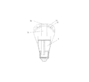
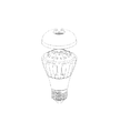
本発明に係るLED照明装置は、中空アウトの構造を有するベースと、ベースの上表面に直接塗布される回路コーティング層と、直接にベースに貼合され、回路コーティング層を介して互いに接続される複数のLED発光チップと、ベースに設けられ、LED発光チップと回路コーティング層とを覆い、熱伝導材料により製造された中実の部品であり、光線の射出面である外表面と、配光面および熱伝導面を含む内表面と、を備えるランプカバーと、を含み、前記配光面は、内表面におけるLED発光チップと対応する内表面エリアに設置され、LED発光チップとの間には隙間が存在し、ベースの上表面と共に配光チャンパーを形成している。前記熱伝導面は内表面におけるベースのLED発光チップが取り付けられた部分以外の部分又はすべての上表面が対応する内表面エリアに設置され、ベースと隙間なく貼合されている。熱伝導面は、少なくとも内表面の中央エリアおよびエッジエリアに分布されている。 The LED lighting device according to the present invention includes a base having a hollow-out structure, a circuit coating layer applied directly to the upper surface of the base, and directly bonded to the base and connected to each other via the circuit coating layer. A plurality of LED light emitting chips, a solid part provided on the base, covering the LED light emitting chips and the circuit coating layer, and made of a heat conductive material, an outer surface that is a light emitting surface, and a light distribution surface And a lamp cover including an inner surface including a heat conducting surface, and the light distribution surface is disposed in an inner surface area corresponding to the LED light emitting chip on the inner surface, and a gap is provided between the LED light emitting chip and the LED light emitting chip. And forms a light distribution champ together with the upper surface of the base. The heat conduction surface is installed in an inner surface area corresponding to the upper surface of a portion other than the portion to which the LED light emitting chip of the base on the inner surface is attached, and is bonded to the base without a gap. The heat conducting surface is distributed at least in the central area and the edge area of the inner surface.
好ましくは、ランプカバーの内表面は配光面及び熱伝導面のみによって構成されている。 Preferably, the inner surface of the lamp cover is constituted only by a light distribution surface and a heat conduction surface.
好ましくは、ランプカバーは透明性セラミックス又はガラスによって製造されている。 Preferably, the lamp cover is made of transparent ceramics or glass.
好ましくは、前記透明性セラミックスはPLZT、CaF2、Y2O3、YAG、多結晶AIONとMgAl2O4の内の一種類又は複数種類の組み合わせから選択される少なくとも一種類の材料が含まれる。 Preferably, the transparent ceramic includes at least one material selected from one or a combination of PLZT, CaF 2 , Y 2 O 3 , YAG, polycrystalline AION and MgAl 2 O 4. .
本発明の発明者は実験を繰り返し、PC、ガラスおよび透明性セラミックスのそれぞれを使用してランプカバーを製造して実験した結果、PCを使用した場合の接合温度の上昇幅が最も高く、透明レンズの接合温度の上昇幅はPCを使用した場合より4℃低く、透明性セラミックスレンズの接合温度の上昇幅はPCを使用した場合より8℃低いことが証明された。従って、本発明では熱伝導性がより優れ、使用中における接合温度の上昇幅がより低いガラスとセラミックスを用いる。 The inventor of the present invention repeated the experiment, manufactured a lamp cover using each of PC, glass and transparent ceramics, and as a result, the increase in the junction temperature when using PC was the highest, and the transparent lens It was proved that the increase in the bonding temperature was 4 ° C. lower than when PC was used, and the increase in the bonding temperature of the transparent ceramic lens was 8 ° C. lower than when PC was used. Therefore, in the present invention, glass and ceramics having better thermal conductivity and a lower increase in bonding temperature during use are used.
好ましくは、前記回路コーティング層は金属材料が含まれる流体又は粉末のコーティング層であり、前記回路コーティング層の厚さは20μm以上である。 Preferably, the circuit coating layer is a fluid or powder coating layer containing a metal material, and the thickness of the circuit coating layer is 20 μm or more.
好ましくは、前記回路コーティング層の金属材料はモリブデン、マンガン、タングステン、銀、金、プラチナ、銀パラジウム合金、銅、アルミ、スズ等のうちの少なくとも一種類又は複数種類の組み合わせである。 Preferably, the metal material of the circuit coating layer is at least one kind or a combination of plural kinds of molybdenum, manganese, tungsten, silver, gold, platinum, silver palladium alloy, copper, aluminum, tin and the like.
好ましくは、発光チップが設置されるベースの上表面は曲面又は複数の平面を組み合わせた形状である。 Preferably, the upper surface of the base on which the light emitting chip is installed has a curved surface or a shape obtained by combining a plurality of flat surfaces.
好ましくは、ランプカバーの外表面は配光の要求に応じて特定の曲面の形状に製造され、ベースと接触する内表面はベースの上表面の形状と対応する曲面又は複数の平面を組み合わせた形状である。 Preferably, the outer surface of the lamp cover is manufactured to have a specific curved surface shape according to light distribution requirements, and the inner surface in contact with the base has a curved surface corresponding to the shape of the upper surface of the base or a combination of a plurality of flat surfaces. It is.
好ましくは、ベースには第一放熱貫通孔が設置されている。 Preferably, the base is provided with a first heat radiating through hole.
好ましくは、ベースは絶縁層が塗布された金属ベース又は絶縁材料によって製造されたベースである。 Preferably, the base is a metal base coated with an insulating layer or a base made of an insulating material.
好ましくは、プラスチック又はセラミックス材料によって製造され、ベースと連通されず、即ちベースと隔てている電源チャンパーをさらに含む。電源チャンパーのハウジング本体とベースとは一つにまとまれても単独構造であってもよく、係止挿入、係止接続、ねじり込み等の方式により互いに接続され、それぞれが独立して放熱を実現できる。また、チップにより生成される熱量の電源に対する影響を低下させ、LED照明装置全体の総合的な放熱能力を向上させる。 Preferably, it further comprises a power supply champ that is made of a plastic or ceramic material and is not in communication with the base, i.e. separated from the base. The housing body and base of the power supply champ may be combined into one or a single structure, and connected to each other by methods such as locking insertion, locking connection, and twisting, and each can achieve heat dissipation independently. . Moreover, the influence with respect to the power supply of the calorie | heat amount produced | generated by a chip | tip is reduced, and the comprehensive heat dissipation capability of the whole LED lighting apparatus is improved.
本発明に係るLED照明装置の構造は、ランプカバーとベースとが貼合されているため、LED発光チップにより生成される熱量はランプカバーによって伝導できるだけでなく、ベースによっても外へ伝導できる。また、ランプカバーの熱伝導面が内表面の中央エリアおよびエッジエリアに分布されているため、エッジのみが接触する従来技術に比べて、ランプカバーとベースとの接触面積が拡大され、ランプカバーの放熱機能を向上させる。本発明の発明者はコンピュータ上の熱シミュレーションソフトウェアで計算し、本発明と同一材料、同一体積、同一パワーのエッジのみが接触する従来技術に比べて、接合温度の上昇幅は少なくとも30℃以上低下させることができる。また、本発明は回路基板を省き、回路コーティング層を直接ベースに塗布しているため、熱抵抗を大幅に低下させ、照明器具全体の放熱効果を向上させる。同時に、ベースが中空アウトの構造であり、ベースとランプカバーにはそれぞれ第一及び第二放熱貫通孔が設置され、LED照明装置全体が各方向のいずれからでも空気の流通が実現されているため、レンズとベースから表面に導出される熱が素早く流通する空気に持ち去られ、照明装置全体の散熱効果を向上させる。 In the structure of the LED lighting device according to the present invention, since the lamp cover and the base are bonded, the amount of heat generated by the LED light emitting chip can be conducted not only by the lamp cover but also by the base. In addition, since the heat conduction surface of the lamp cover is distributed in the center area and the edge area of the inner surface, the contact area between the lamp cover and the base is increased compared to the conventional technology in which only the edges are in contact with each other. Improve heat dissipation function. The inventor of the present invention calculates with a thermal simulation software on a computer, and the increase in the junction temperature is reduced by at least 30 ° C. compared to the prior art in which only edges of the same material, the same volume, and the same power contact as the present invention. Can be made. Moreover, since the present invention omits the circuit board and directly applies the circuit coating layer to the base, the thermal resistance is greatly reduced and the heat dissipation effect of the entire lighting fixture is improved. At the same time, since the base has a hollow-out structure, the base and the lamp cover are provided with first and second heat radiating through holes, respectively, and the entire LED lighting device is capable of air circulation from any direction. The heat derived from the lens and base to the surface is taken away by the rapidly flowing air, improving the heat dissipation effect of the entire lighting device.
同時に、発明者は繰り返して実験の検証を行い、得られた実験の結果はコンピュータ上の熱シミュレーションソフトウェアによってシミュレーションして得られた結果と完全に一致する。従って、本発明の技術的解決手段はLED照明装置全体の放熱効果を向上させる面において、突破的進歩を遂げた。 At the same time, the inventor repeatedly verifies the experiment, and the result of the experiment obtained is in complete agreement with the result obtained by simulation with the thermal simulation software on the computer. Therefore, the technical solution of the present invention has made a breakthrough in improving the heat dissipation effect of the entire LED lighting device.
従来の技術に比べて、本発明は以下のような有益な効果を奏する。 Compared with the prior art, the present invention has the following beneficial effects.
熱伝導性能が比較的に優れた材料をランプカバーに使用しているため、チップにより生成される熱量はベースを通して放熱できるだけでなく、ランプカバーの内表面に設置され、ベースと直接に貼合されている熱伝導面によっても外へ伝導できる。また、本発明の好ましい構造、たとえば放熱貫通孔および中空アウトのベースは放熱機能を更に向上させることができる。これらによって装置全体が全方向に向けて放熱でき、装置の放熱性能を大幅に向上させ、装置の使用寿命を延長させる。さらに、単独に設置されている電源チャンパーはチップにより生成される熱量と電源により生成される熱量とをそれぞれ異なる構造によって外へ放出させることができるため、チップにより生成される熱量の電源に及ぼす影響を減らし、過度の熱の電源に及ぼす影響を低下させる。 Because the lamp cover is made of a material with relatively good heat conduction performance, the amount of heat generated by the chip can be dissipated through the base, and it is installed on the inner surface of the lamp cover and bonded directly to the base. It can also be conducted to the outside by the heat conduction surface. Further, the preferred structure of the present invention, for example, the heat radiation through hole and the base of the hollow out, can further improve the heat radiation function. As a result, the entire apparatus can dissipate heat in all directions, greatly improving the heat dissipation performance of the apparatus and extending the service life of the apparatus. Furthermore, since the power supply champ installed independently can release the amount of heat generated by the chip and the amount of heat generated by the power supply by different structures, the influence of the amount of heat generated by the chip on the power supply Reduce the effect of excessive heat on the power supply.
本発明の製品は如何なる方向で取り付けても、360度全方位での空気流通を実現できるため、照明器具自体が生じる熱を放出でき、ジャンクション温度の昇温幅を低下させる The product of the present invention can realize 360 degree omnidirectional air circulation regardless of the direction of installation, so it can release the heat generated by the luminaire itself and lower the temperature range of the junction temperature.
さらに、放熱性能の向上により、装置の体積を増加しない状況で出力がさらに大きい照明装置を製造でき、装置の照明の明るさを向上させとともに、生活および工業上の使用においてLED照明装置の使用範囲と自由度を向上させることができる。 Furthermore, by improving the heat dissipation performance, it is possible to manufacture a lighting device with a higher output without increasing the volume of the device, improving the brightness of the lighting of the device, and using the LED lighting device in daily life and industrial use And the degree of freedom can be improved.
以下、図面を参照しながら、非限定的な実施例に対して詳細に説明することにより、本発明のその他の特徴、目的および利点はより明確になる。 Hereinafter, other features, objects, and advantages of the present invention will become more apparent by describing in detail non-limiting embodiments with reference to the drawings.
以下、具体的な実施例により本発明を詳しく説明する。以下の実施例はいわゆる当業者が本発明をより理解しやすくするためのものであり、いかなる形式で本発明を限定するものではない。また、いわゆる当業者であれば、本発明の技術的思想を逸脱しないことを前提として、さらなる若干の変形及び改善をしても可能である。これらはいずれも本発明の保護範囲に属することはいうまでもない。 Hereinafter, the present invention will be described in detail by way of specific examples. The following examples are intended to make it easier for those skilled in the art to understand the present invention and are not intended to limit the present invention in any way. Further, a so-called person skilled in the art can make further slight modifications and improvements on the premise that the technical idea of the present invention is not deviated. Needless to say, these belong to the protection scope of the present invention.
本発明に係るLED照明装置は、ベース、発光チップ、回路コーティング層、ランプカバー、電源チャンパーを含む。ランプカバーは中実の熱伝導材料によって製造され、良好な熱伝導機能を有する。発光チップはベースに固定されており、ランプカバーはベースに設置され、発光チップを覆う。また、ランプカバーは、発光チップに対応するエリア(即ち配光面)以外の内表面を熱伝導面としてベースと接触することにより放熱機能を実現し、ランプカバーにおける発光チップに対応するエリアの内表面は設計必要に応じて特定の空間構造の形状に形成され、光強度の分布を変化させる。ここで、熱伝導面はランプカバーの内表面の一部として、それ自体は光線の反射及び/又は屈折の特性を利用して配光に関与することができる。このため、熱伝導面を利用して配光に関与する技術案も同様に本発明により保護される非制限的な実施例に属する。 The LED lighting device according to the present invention includes a base, a light emitting chip, a circuit coating layer, a lamp cover, and a power supply champ. The lamp cover is made of a solid heat conducting material and has a good heat conducting function. The light emitting chip is fixed to the base, and the lamp cover is installed on the base and covers the light emitting chip. In addition, the lamp cover realizes a heat dissipation function by contacting the base with the inner surface other than the area corresponding to the light emitting chip (that is, the light distribution surface) as a heat conducting surface, and the lamp cover covers the light emitting chip within the area corresponding to the light emitting chip. The surface is formed in the shape of a specific spatial structure according to design needs, and the distribution of light intensity is changed. Here, the heat conducting surface is part of the inner surface of the lamp cover, and can itself participate in the light distribution by utilizing the reflection and / or refraction characteristics of the light beam. For this reason, the technical solutions related to the light distribution using the heat conducting surface also belong to the non-limiting examples protected by the present invention.
ベースの上表面は曲面又は複数の平面を組み合わせた形状である。ベースは中空アウトの構造を使用することにより空気の流通を向上させ、放熱効果を強める。例えば、ベースの中央部に第一放熱貫通孔を設置することにより空気の流通を向上させ、放熱効果を強め、同様に、ランプカバーにおけるベースに対応する位置に第二放熱貫通孔を設置する。発光チップの数量は複数である。 The upper surface of the base has a curved surface or a combination of a plurality of planes. The base uses a hollow-out structure to improve air flow and enhance heat dissipation. For example, the first heat radiating through hole is provided in the center of the base to improve the air flow and enhance the heat radiating effect. Similarly, the second heat radiating through hole is provided at a position corresponding to the base in the lamp cover. There are a plurality of light emitting chips.
ランプカバーは配光機能を有し、セラミックス、ガラス又はその他の光透過性能を有する高熱伝導材料から選択されたものである。ランプカバーの外表面は実際の必要に応じて、特定の形状に設計される。ベースは電源チャンパーに設置され、それぞれが単独で放熱を実現できる。ベースは金属ベースに絶縁層を塗布したものや、セラミックス製のベース等であってよい。
(実施例1)
The lamp cover has a light distribution function and is selected from ceramics, glass or other highly heat-conductive materials having light transmission performance. The outer surface of the lamp cover is designed to a specific shape according to actual needs. The base is installed in the power supply champ, and each can achieve heat dissipation. The base may be a metal base coated with an insulating layer, a ceramic base, or the like.
Example 1
続いて、図1および図2を参照しながら、第一実施例ついて具体的に説明する。 Next, the first embodiment will be specifically described with reference to FIGS. 1 and 2.
新型LED照明装置は主に、ベース、22個のLED発光チップ、回路コーティング層および高熱伝導ランプカバーを含む。ベースは上表面が曲面のセラミックスベースであり、ベースの中央部には第一放熱貫通孔が設けられ、ベースの上表面における第一放熱貫通孔以外のその他の部分には回路コーティング層が直接塗布されており、回路コーティング層は導電性を有する銀ペーストである。発光チップは直接ベースに貼合され、回路コーティング層によって互いに接続されている。ランプカバーは中実の透光性セラミックスであり、多結晶AIONによって製造される。ランプカバーにおけるベースの第一放熱貫通孔に対応する中央部位置には第二放熱貫通孔が設けられ、空気の流通を実現する。ランプカバーにおけるベースに接触する内表面はベースの形状に対応する曲面であって、ベースに直接接触し、且つベースを覆い、LED発光チップおよび回路コーティング層を内側にパッケージングする。配光面は、LED発光チップと対応する内表面に設置され、LED発光チップとは貼合されておらず、ベースの上表面と共に配光チャンパーを形成している。熱伝導面は、少なくともランプカバーの内表面の中央エリアとエッジエリアに分布され、ベースの上表面と隙間なく貼合されて透光及び放熱の作用を実現する。ベースは完全な中空アウトの構造であって、対流による換気を実現できる。電源チャンパーは、セラミックスによって製造され、ベースとは一つまとまった構造であり、ベースとは連通されておらず、それぞれ単独で放熱を実現できる。
(実施例2)
The new LED lighting device mainly includes a base, 22 LED light emitting chips, a circuit coating layer, and a high heat conduction lamp cover. The base is a ceramic base with a curved upper surface. A first heat dissipation through hole is provided in the center of the base, and a circuit coating layer is applied directly to the rest of the base upper surface other than the first heat dissipation through hole. The circuit coating layer is a conductive silver paste. The light emitting chips are directly bonded to the base and connected to each other by a circuit coating layer. The lamp cover is a solid translucent ceramic and is manufactured from polycrystalline AION. A second heat radiating through hole is provided at the center position corresponding to the first heat radiating through hole of the base of the lamp cover, thereby realizing air circulation. The inner surface of the lamp cover that contacts the base is a curved surface corresponding to the shape of the base, directly contacts the base and covers the base, and the LED light emitting chip and the circuit coating layer are packaged inside. The light distribution surface is installed on the inner surface corresponding to the LED light emitting chip, is not bonded to the LED light emitting chip, and forms a light distribution champ together with the upper surface of the base. The heat conductive surface is distributed at least in the central area and the edge area of the inner surface of the lamp cover, and is bonded to the upper surface of the base without any gap to realize the light transmitting and heat radiating action. The base has a completely hollow-out structure and can achieve convection ventilation. The power supply champ is made of ceramics and has a single structure with the base, and is not in communication with the base.
(Example 2)
続いて、図4を参照しながら、第二実施例について具体的に説明する。 Next, the second embodiment will be specifically described with reference to FIG.
新型LED照明装置は主に、ベース、27個のLED発光チップ、回路コーティング層およびランプカバーを含む。ベースは、上表面に絶縁材料が塗布されたアルミベースであり、上表面は多角錐台の形状である。ベースの上表面における第一放熱貫通孔以外のその他の部分には回路コーティング層が直接塗布され、回路コーティング層は導電性を有するパラジウム銀合金スラリーである。LED発光チップは、直接ベースに貼合され、回路コーティング層によって互いに接続されている。ランプカバーは中実の透光性セラミックスであり、MgAl2O4によって製造される。ランプカバーにおけるベースの第一放熱貫通孔と対応する中央部位置には第二放熱貫通孔が設けられ、空気の流通を実現する。ランプカバーにおけるベースに接触する内表面はベースの形状と対応する複数の平面を組み合わせた形状であり、ベースと直接接触し且つベースを覆い、LED発光チップと回路コーティング層を内側にパッケージングする。配光面は、LED発光チップと対応する内表面に設置され、LED発光チップとは貼合されておらず、ベースの上表面と共に配光チャンパーを形成している。熱伝導面は、少なくともランプカバーの内表面の中央エリアとエッジエリアに分布し、ベースの上表面と隙間なく貼合されて透光及び放熱の作用を実現する。ベースは完全な中空アウトの構造であり、対流による換気を実現できる。電源チャンパーは、プラスチックによって製造され、独立な構造であり、ベースとは連通されていない。ベースと電源チャンパーとはソケットの方式により接続され、それぞれが単独で放熱を実現できる。電源チャンパーとベースとは係止又はその他の方法によって接続が可能である。 The new LED lighting device mainly includes a base, 27 LED light emitting chips, a circuit coating layer and a lamp cover. The base is an aluminum base having an upper surface coated with an insulating material, and the upper surface has a polygonal frustum shape. A circuit coating layer is directly applied to other portions other than the first heat dissipation through hole on the upper surface of the base, and the circuit coating layer is a palladium-silver alloy slurry having conductivity. The LED light emitting chips are directly bonded to the base and connected to each other by a circuit coating layer. The lamp cover is a solid translucent ceramic and is made of MgAl 2 O 4 . A second heat radiating through hole is provided at a central position corresponding to the first heat radiating through hole of the base in the lamp cover, thereby realizing air circulation. The inner surface of the lamp cover that contacts the base has a shape combining a plurality of planes corresponding to the shape of the base, and is in direct contact with and covers the base, and the LED light emitting chip and the circuit coating layer are packaged inside. The light distribution surface is installed on the inner surface corresponding to the LED light emitting chip, is not bonded to the LED light emitting chip, and forms a light distribution champ together with the upper surface of the base. The heat conduction surface is distributed at least in the central area and the edge area of the inner surface of the lamp cover, and is bonded to the upper surface of the base without any gap to realize the light transmitting and heat radiating action. The base has a completely hollow-out structure, and ventilation by convection can be realized. The power champ is made of plastic and has an independent structure and is not in communication with the base. The base and the power supply champ are connected by a socket method, and each can realize heat dissipation. The power champ and the base can be connected by locking or other methods.
以上のとおり、本発明に係る具体的な実施例について説明したが、本発明は上記の特定の実施方法に限定されず、いわゆる当業者は特許請求の範囲内において、各種の変形又は変更を行うことができ、これらは本発明の本質的な内容に対して影響を与えないことを理解すべきである。 As described above, specific embodiments according to the present invention have been described. However, the present invention is not limited to the specific implementation methods described above, and so-called persons skilled in the art make various modifications or changes within the scope of the claims. It should be understood that these do not affect the essential content of the present invention.
1 ベース、
2 発光チップ、
3 ランプカバー、
31 配光面、
32 熱伝導面、
4 電源チャンパー、
51 第一放熱貫通孔、
52 第一放熱貫通孔。
1 base,
2 light emitting chip,
3 Lamp cover,
31 Light distribution surface,
32 heat conduction surface,
4 Power champ,
51 1st heat dissipation through hole,
52 1st heat dissipation through hole.
Claims (11)
Applications Claiming Priority (3)
| Application Number | Priority Date | Filing Date | Title |
|---|---|---|---|
| CN201410040152.4 | 2014-01-27 | ||
| CN201410040152.4A CN103791439B (en) | 2014-01-27 | 2014-01-27 | Novel LED lighting device |
| PCT/CN2014/076052 WO2015109675A1 (en) | 2014-01-27 | 2014-04-23 | Novel led lighting apparatus |
Publications (2)
| Publication Number | Publication Date |
|---|---|
| JP2017508246A true JP2017508246A (en) | 2017-03-23 |
| JP6360180B2 JP6360180B2 (en) | 2018-07-18 |
Family
ID=50667356
Family Applications (1)
| Application Number | Title | Priority Date | Filing Date |
|---|---|---|---|
| JP2016548056A Active JP6360180B2 (en) | 2014-01-27 | 2014-04-23 | LED lighting device |
Country Status (7)
| Country | Link |
|---|---|
| US (1) | US20160341413A1 (en) |
| EP (1) | EP3101332A1 (en) |
| JP (1) | JP6360180B2 (en) |
| KR (1) | KR20160132825A (en) |
| CN (1) | CN103791439B (en) |
| CA (1) | CA2937939C (en) |
| WO (1) | WO2015109675A1 (en) |
Families Citing this family (5)
| Publication number | Priority date | Publication date | Assignee | Title |
|---|---|---|---|---|
| KR20160132824A (en) * | 2014-01-27 | 2016-11-21 | 상하이 산시 일렉트로닉 엔지니어링 씨오., 엘티디 | Led lighting apparatus |
| KR20160133426A (en) * | 2014-01-27 | 2016-11-22 | 상하이 산시 일렉트로닉 엔지니어링 씨오., 엘티디 | Led lighting apparatus, light shade, and circuit manufacturing method for the apparatus |
| CN104566309A (en) * | 2014-12-25 | 2015-04-29 | 上海三思电子工程有限公司 | Manufacturing method for heat sink and lamp with heat sink |
| CN104659027A (en) * | 2015-02-09 | 2015-05-27 | 上海三思电子工程有限公司 | LED light emitting body and manufacturing method thereof |
| CN106151923A (en) * | 2015-03-25 | 2016-11-23 | 上海三思电子工程有限公司 | A kind of LED light device |
Citations (5)
| Publication number | Priority date | Publication date | Assignee | Title |
|---|---|---|---|---|
| JP2010108768A (en) * | 2008-10-30 | 2010-05-13 | Sharp Corp | Light source unit and lighting device |
| CN202092058U (en) * | 2011-04-30 | 2011-12-28 | 深圳市易特照明有限公司 | Ceramic substrate of light-emitting diode (LED) lamp and LED lamp |
| JP2012119313A (en) * | 2010-11-30 | 2012-06-21 | Samsung Led Co Ltd | Led lamp |
| JP2013080690A (en) * | 2011-03-11 | 2013-05-02 | Toshiba Corp | Lighting device |
| JP2013517609A (en) * | 2010-01-20 | 2013-05-16 | オスラム ゲーエムベーハー | Lighting device |
Family Cites Families (28)
| Publication number | Priority date | Publication date | Assignee | Title |
|---|---|---|---|---|
| US7728345B2 (en) * | 2001-08-24 | 2010-06-01 | Cao Group, Inc. | Semiconductor light source for illuminating a physical space including a 3-dimensional lead frame |
| JP3813123B2 (en) * | 2002-12-25 | 2006-08-23 | 株式会社沖データ | Semiconductor device and LED head |
| JP4031784B2 (en) * | 2004-07-28 | 2008-01-09 | シャープ株式会社 | Light emitting module and manufacturing method thereof |
| US8661660B2 (en) * | 2005-09-22 | 2014-03-04 | The Artak Ter-Hovhanissian Patent Trust | Process for manufacturing LED lighting with integrated heat sink |
| EA017207B1 (en) * | 2007-07-04 | 2012-10-30 | Агк Гласс Юроп | Led light panel |
| TW201031859A (en) * | 2009-02-23 | 2010-09-01 | Taiwan Green Point Entpr Co | High efficiency luminous body |
| CN102449374B (en) * | 2009-05-28 | 2016-05-11 | 皇家飞利浦电子股份有限公司 | Ceramic illumination device |
| DE102009035370A1 (en) * | 2009-07-30 | 2011-02-03 | Osram Gesellschaft mit beschränkter Haftung | lamp |
| CN101666439A (en) * | 2009-09-16 | 2010-03-10 | 鹤山丽得电子实业有限公司 | Liquid cooling LED lamp |
| US8827508B2 (en) * | 2009-10-22 | 2014-09-09 | Thermal Solution Resources, Llc | Overmolded LED light assembly and method of manufacture |
| DE102010001046A1 (en) * | 2010-01-20 | 2011-07-21 | Osram Gesellschaft mit beschränkter Haftung, 81543 | lighting device |
| CN102135268A (en) * | 2010-01-27 | 2011-07-27 | 可成科技股份有限公司 | Method for manufacturing light-emitting diode lamp |
| AT14251U1 (en) * | 2010-04-09 | 2015-07-15 | Bartenbach Christian | Led lamp |
| TWI467115B (en) * | 2010-08-06 | 2015-01-01 | Ind Tech Res Inst | Light source apparatus with high heat dissipation efficiency |
| TW201207310A (en) * | 2010-08-13 | 2012-02-16 | Foxsemicon Integrated Tech Inc | LED lamp and method for manufacturing a heat sink of the LED lamp |
| DE102010043918B4 (en) * | 2010-11-15 | 2016-05-12 | Osram Gmbh | Semiconductor lamp |
| CN102072428B (en) * | 2010-12-20 | 2013-05-08 | 鸿富锦精密工业(深圳)有限公司 | Light emitting diode (LED) daylight lamp |
| CN102809137A (en) * | 2011-06-01 | 2012-12-05 | 弘凯光电股份有限公司 | Lamp heat radiation structure manufacturing method and lamp component manufacturing method |
| KR101253199B1 (en) * | 2011-07-25 | 2013-04-10 | 엘지전자 주식회사 | Lighting apparatus |
| CN102261589B (en) * | 2011-07-28 | 2013-07-17 | 厦门立明光电有限公司 | Lighting LED lamp |
| CN202349777U (en) * | 2011-11-24 | 2012-07-25 | 上海天逸电器有限公司 | Machine tool illumination lamp with metal aluminum shell |
| US20130148355A1 (en) * | 2011-12-09 | 2013-06-13 | Switch Bulb Company, Inc. | Led bulb with liquid-cooled drive electronics |
| CN202442139U (en) * | 2012-01-10 | 2012-09-19 | 江西惜能光电有限公司 | Plastic LED (light emitting diode) lamp |
| US20140016316A1 (en) * | 2012-07-12 | 2014-01-16 | Elementech International Co., Ltd. | Illuminant device |
| CN202868352U (en) * | 2012-07-25 | 2013-04-10 | 宁波圣彼电气有限公司 | Heat dissipation LED bulb |
| CN202791524U (en) * | 2012-09-21 | 2013-03-13 | 深圳市浩原义光电科技有限公司 | LED (light-emitting diode) bulb lamp with PC (polycarbonate) shell |
| CN202955537U (en) * | 2012-12-04 | 2013-05-29 | 上海三思电子工程有限公司 | LED (Light-Emitting Diode) bulb lamp capable of realizing wide-angle luminescence |
| KR20160132824A (en) * | 2014-01-27 | 2016-11-21 | 상하이 산시 일렉트로닉 엔지니어링 씨오., 엘티디 | Led lighting apparatus |
-
2014
- 2014-01-27 CN CN201410040152.4A patent/CN103791439B/en active Active
- 2014-04-23 EP EP14880067.5A patent/EP3101332A1/en not_active Ceased
- 2014-04-23 KR KR1020167023574A patent/KR20160132825A/en active Search and Examination
- 2014-04-23 US US15/114,835 patent/US20160341413A1/en not_active Abandoned
- 2014-04-23 WO PCT/CN2014/076052 patent/WO2015109675A1/en active Application Filing
- 2014-04-23 CA CA2937939A patent/CA2937939C/en active Active
- 2014-04-23 JP JP2016548056A patent/JP6360180B2/en active Active
Patent Citations (5)
| Publication number | Priority date | Publication date | Assignee | Title |
|---|---|---|---|---|
| JP2010108768A (en) * | 2008-10-30 | 2010-05-13 | Sharp Corp | Light source unit and lighting device |
| JP2013517609A (en) * | 2010-01-20 | 2013-05-16 | オスラム ゲーエムベーハー | Lighting device |
| JP2012119313A (en) * | 2010-11-30 | 2012-06-21 | Samsung Led Co Ltd | Led lamp |
| JP2013080690A (en) * | 2011-03-11 | 2013-05-02 | Toshiba Corp | Lighting device |
| CN202092058U (en) * | 2011-04-30 | 2011-12-28 | 深圳市易特照明有限公司 | Ceramic substrate of light-emitting diode (LED) lamp and LED lamp |
Also Published As
| Publication number | Publication date |
|---|---|
| WO2015109675A1 (en) | 2015-07-30 |
| KR20160132825A (en) | 2016-11-21 |
| CN103791439B (en) | 2015-05-06 |
| EP3101332A4 (en) | 2016-12-07 |
| JP6360180B2 (en) | 2018-07-18 |
| CA2937939A1 (en) | 2015-07-30 |
| US20160341413A1 (en) | 2016-11-24 |
| CA2937939C (en) | 2020-08-04 |
| CN103791439A (en) | 2014-05-14 |
| EP3101332A1 (en) | 2016-12-07 |
Similar Documents
| Publication | Publication Date | Title |
|---|---|---|
| KR101086548B1 (en) | Led lamp module and fabrication method thereof | |
| JP4880358B2 (en) | Light source substrate and illumination device using the same | |
| JP5082083B2 (en) | LED lighting device | |
| JP6360180B2 (en) | LED lighting device | |
| JP2009277586A (en) | Electric lamp type led luminaire | |
| WO2009000106A1 (en) | Led lighting device | |
| JP2010108768A (en) | Light source unit and lighting device | |
| JP4683013B2 (en) | Light emitting device | |
| JP6343812B2 (en) | COATING TYPE STRUCTURED CIRCUIT MANUFACTURING METHOD, LED BULB LAMP AND ELECTRONIC COMPONENT WITHOUT CIRCUIT PANEL | |
| JP2011096594A (en) | Bulb type led lamp | |
| KR20170005664A (en) | Lighting device module | |
| WO2017124784A1 (en) | Wide-angle light emitting led filament lamp | |
| JP5618331B2 (en) | Lighting device | |
| TW201034266A (en) | Heat dissipation module for a light emitting device and light emitting diode device having the same | |
| JP6495307B2 (en) | LED lighting device | |
| KR20170030181A (en) | LED module having heat property construction | |
| JP3158994U (en) | Circuit board | |
| CN209744084U (en) | LED light source module and lighting device | |
| CN209856797U (en) | LED light source module and lighting device | |
| WO2016029808A1 (en) | Light emission and heat dissipation structure of led light source and light emission and heat dissipation method therefor | |
| CN215335836U (en) | LED light source substrate | |
| TWI523271B (en) | Plug-in light-emitting unit and light-emitting device | |
| KR20130003414A (en) | Led lamp | |
| JP2007158086A (en) | Shape of mounting metal substrate for led element and led element mounting substrate | |
| CN112066276A (en) | LED light source module and lighting device |
Legal Events
| Date | Code | Title | Description |
|---|---|---|---|
| A521 | Request for written amendment filed |
Free format text: JAPANESE INTERMEDIATE CODE: A523 Effective date: 20161214 |
|
| A131 | Notification of reasons for refusal |
Free format text: JAPANESE INTERMEDIATE CODE: A131 Effective date: 20170801 |
|
| A977 | Report on retrieval |
Free format text: JAPANESE INTERMEDIATE CODE: A971007 Effective date: 20170728 |
|
| A521 | Request for written amendment filed |
Free format text: JAPANESE INTERMEDIATE CODE: A523 Effective date: 20171101 |
|
| A02 | Decision of refusal |
Free format text: JAPANESE INTERMEDIATE CODE: A02 Effective date: 20171226 |
|
| A521 | Request for written amendment filed |
Free format text: JAPANESE INTERMEDIATE CODE: A523 Effective date: 20180423 |
|
| A911 | Transfer to examiner for re-examination before appeal (zenchi) |
Free format text: JAPANESE INTERMEDIATE CODE: A911 Effective date: 20180427 |
|
| TRDD | Decision of grant or rejection written | ||
| A01 | Written decision to grant a patent or to grant a registration (utility model) |
Free format text: JAPANESE INTERMEDIATE CODE: A01 Effective date: 20180529 |
|
| A61 | First payment of annual fees (during grant procedure) |
Free format text: JAPANESE INTERMEDIATE CODE: A61 Effective date: 20180621 |
|
| R150 | Certificate of patent or registration of utility model |
Ref document number: 6360180 Country of ref document: JP Free format text: JAPANESE INTERMEDIATE CODE: R150 |
|
| R250 | Receipt of annual fees |
Free format text: JAPANESE INTERMEDIATE CODE: R250 |
|
| R250 | Receipt of annual fees |
Free format text: JAPANESE INTERMEDIATE CODE: R250 |
|
| R250 | Receipt of annual fees |
Free format text: JAPANESE INTERMEDIATE CODE: R250 |