JP2017501879A - Zinc-based lead-free solder composition - Google Patents
Zinc-based lead-free solder composition Download PDFInfo
- Publication number
- JP2017501879A JP2017501879A JP2016536807A JP2016536807A JP2017501879A JP 2017501879 A JP2017501879 A JP 2017501879A JP 2016536807 A JP2016536807 A JP 2016536807A JP 2016536807 A JP2016536807 A JP 2016536807A JP 2017501879 A JP2017501879 A JP 2017501879A
- Authority
- JP
- Japan
- Prior art keywords
- solder
- zinc
- weight
- solder composition
- layer
- Prior art date
- Legal status (The legal status is an assumption and is not a legal conclusion. Google has not performed a legal analysis and makes no representation as to the accuracy of the status listed.)
- Pending
Links
- 229910000679 solder Inorganic materials 0.000 title claims abstract description 201
- 239000000203 mixture Substances 0.000 title claims abstract description 110
- 239000011701 zinc Substances 0.000 title claims abstract description 81
- HCHKCACWOHOZIP-UHFFFAOYSA-N Zinc Chemical compound [Zn] HCHKCACWOHOZIP-UHFFFAOYSA-N 0.000 title claims abstract description 66
- 229910052725 zinc Inorganic materials 0.000 title claims abstract description 66
- GYHNNYVSQQEPJS-UHFFFAOYSA-N Gallium Chemical compound [Ga] GYHNNYVSQQEPJS-UHFFFAOYSA-N 0.000 claims abstract description 31
- FYYHWMGAXLPEAU-UHFFFAOYSA-N Magnesium Chemical compound [Mg] FYYHWMGAXLPEAU-UHFFFAOYSA-N 0.000 claims abstract description 31
- 239000011777 magnesium Substances 0.000 claims abstract description 31
- 229910052733 gallium Inorganic materials 0.000 claims abstract description 29
- 229910052749 magnesium Inorganic materials 0.000 claims abstract description 29
- 229910052732 germanium Inorganic materials 0.000 claims abstract description 23
- GNPVGFCGXDBREM-UHFFFAOYSA-N germanium atom Chemical compound [Ge] GNPVGFCGXDBREM-UHFFFAOYSA-N 0.000 claims abstract description 23
- 229910052782 aluminium Inorganic materials 0.000 claims abstract description 21
- XAGFODPZIPBFFR-UHFFFAOYSA-N aluminium Chemical compound [Al] XAGFODPZIPBFFR-UHFFFAOYSA-N 0.000 claims abstract description 21
- 229910052779 Neodymium Inorganic materials 0.000 claims description 4
- QEFYFXOXNSNQGX-UHFFFAOYSA-N neodymium atom Chemical compound [Nd] QEFYFXOXNSNQGX-UHFFFAOYSA-N 0.000 claims description 4
- 230000008018 melting Effects 0.000 abstract description 13
- 238000002844 melting Methods 0.000 abstract description 13
- 238000004100 electronic packaging Methods 0.000 abstract description 8
- 239000010949 copper Substances 0.000 description 67
- RYGMFSIKBFXOCR-UHFFFAOYSA-N Copper Chemical compound [Cu] RYGMFSIKBFXOCR-UHFFFAOYSA-N 0.000 description 52
- 229910052802 copper Inorganic materials 0.000 description 52
- PXHVJJICTQNCMI-UHFFFAOYSA-N Nickel Chemical compound [Ni] PXHVJJICTQNCMI-UHFFFAOYSA-N 0.000 description 32
- 230000004888 barrier function Effects 0.000 description 27
- 229910052751 metal Inorganic materials 0.000 description 22
- 239000002184 metal Substances 0.000 description 22
- 238000000034 method Methods 0.000 description 20
- 238000009736 wetting Methods 0.000 description 20
- 230000008569 process Effects 0.000 description 17
- 229910052759 nickel Inorganic materials 0.000 description 16
- 239000002019 doping agent Substances 0.000 description 10
- 238000012360 testing method Methods 0.000 description 9
- 238000004519 manufacturing process Methods 0.000 description 8
- 238000005452 bending Methods 0.000 description 7
- 239000007788 liquid Substances 0.000 description 6
- 230000003647 oxidation Effects 0.000 description 6
- 238000007254 oxidation reaction Methods 0.000 description 6
- 239000000758 substrate Substances 0.000 description 6
- 229910000881 Cu alloy Inorganic materials 0.000 description 5
- 238000009713 electroplating Methods 0.000 description 5
- 230000001737 promoting effect Effects 0.000 description 5
- QPLDLSVMHZLSFG-UHFFFAOYSA-N Copper oxide Chemical compound [Cu]=O QPLDLSVMHZLSFG-UHFFFAOYSA-N 0.000 description 4
- 239000005751 Copper oxide Substances 0.000 description 4
- KDLHZDBZIXYQEI-UHFFFAOYSA-N Palladium Chemical compound [Pd] KDLHZDBZIXYQEI-UHFFFAOYSA-N 0.000 description 4
- ATJFFYVFTNAWJD-UHFFFAOYSA-N Tin Chemical compound [Sn] ATJFFYVFTNAWJD-UHFFFAOYSA-N 0.000 description 4
- 229910000431 copper oxide Inorganic materials 0.000 description 4
- 238000007772 electroless plating Methods 0.000 description 4
- 238000001125 extrusion Methods 0.000 description 4
- 238000012986 modification Methods 0.000 description 4
- 230000004048 modification Effects 0.000 description 4
- BASFCYQUMIYNBI-UHFFFAOYSA-N platinum Chemical compound [Pt] BASFCYQUMIYNBI-UHFFFAOYSA-N 0.000 description 4
- 229910052718 tin Inorganic materials 0.000 description 4
- 239000011135 tin Substances 0.000 description 4
- 229910045601 alloy Inorganic materials 0.000 description 3
- 239000000956 alloy Substances 0.000 description 3
- 238000004458 analytical method Methods 0.000 description 3
- QVGXLLKOCUKJST-UHFFFAOYSA-N atomic oxygen Chemical compound [O] QVGXLLKOCUKJST-UHFFFAOYSA-N 0.000 description 3
- 238000000921 elemental analysis Methods 0.000 description 3
- 238000002474 experimental method Methods 0.000 description 3
- 229910052738 indium Inorganic materials 0.000 description 3
- 229910000765 intermetallic Inorganic materials 0.000 description 3
- 239000000463 material Substances 0.000 description 3
- 239000000155 melt Substances 0.000 description 3
- 239000001301 oxygen Substances 0.000 description 3
- 229910052760 oxygen Inorganic materials 0.000 description 3
- 230000000737 periodic effect Effects 0.000 description 3
- 238000005476 soldering Methods 0.000 description 3
- IJGRMHOSHXDMSA-UHFFFAOYSA-N Atomic nitrogen Chemical compound N#N IJGRMHOSHXDMSA-UHFFFAOYSA-N 0.000 description 2
- 229910000990 Ni alloy Inorganic materials 0.000 description 2
- BQCADISMDOOEFD-UHFFFAOYSA-N Silver Chemical compound [Ag] BQCADISMDOOEFD-UHFFFAOYSA-N 0.000 description 2
- 238000007792 addition Methods 0.000 description 2
- 230000002411 adverse Effects 0.000 description 2
- 239000012298 atmosphere Substances 0.000 description 2
- 230000015572 biosynthetic process Effects 0.000 description 2
- 238000011161 development Methods 0.000 description 2
- 239000012530 fluid Substances 0.000 description 2
- 230000004907 flux Effects 0.000 description 2
- PCHJSUWPFVWCPO-UHFFFAOYSA-N gold Chemical compound [Au] PCHJSUWPFVWCPO-UHFFFAOYSA-N 0.000 description 2
- 229910052737 gold Inorganic materials 0.000 description 2
- 239000010931 gold Substances 0.000 description 2
- APFVFJFRJDLVQX-UHFFFAOYSA-N indium atom Chemical compound [In] APFVFJFRJDLVQX-UHFFFAOYSA-N 0.000 description 2
- 238000005259 measurement Methods 0.000 description 2
- 238000000879 optical micrograph Methods 0.000 description 2
- 230000001590 oxidative effect Effects 0.000 description 2
- 229910052763 palladium Inorganic materials 0.000 description 2
- 238000007747 plating Methods 0.000 description 2
- 229910052697 platinum Inorganic materials 0.000 description 2
- 229910052709 silver Inorganic materials 0.000 description 2
- 239000004332 silver Substances 0.000 description 2
- 230000035882 stress Effects 0.000 description 2
- JBQYATWDVHIOAR-UHFFFAOYSA-N tellanylidenegermanium Chemical compound [Te]=[Ge] JBQYATWDVHIOAR-UHFFFAOYSA-N 0.000 description 2
- KWSLGOVYXMQPPX-UHFFFAOYSA-N 5-[3-(trifluoromethyl)phenyl]-2h-tetrazole Chemical compound FC(F)(F)C1=CC=CC(C2=NNN=N2)=C1 KWSLGOVYXMQPPX-UHFFFAOYSA-N 0.000 description 1
- 102000041347 CAS family Human genes 0.000 description 1
- 108091075761 CAS family Proteins 0.000 description 1
- OYPRJOBELJOOCE-UHFFFAOYSA-N Calcium Chemical compound [Ca] OYPRJOBELJOOCE-UHFFFAOYSA-N 0.000 description 1
- 229910052684 Cerium Inorganic materials 0.000 description 1
- 229910052692 Dysprosium Inorganic materials 0.000 description 1
- 229910052691 Erbium Inorganic materials 0.000 description 1
- 229910052693 Europium Inorganic materials 0.000 description 1
- 229910052688 Gadolinium Inorganic materials 0.000 description 1
- 229910052689 Holmium Inorganic materials 0.000 description 1
- UFHFLCQGNIYNRP-UHFFFAOYSA-N Hydrogen Chemical compound [H][H] UFHFLCQGNIYNRP-UHFFFAOYSA-N 0.000 description 1
- 229910052765 Lutetium Inorganic materials 0.000 description 1
- ZOKXTWBITQBERF-UHFFFAOYSA-N Molybdenum Chemical compound [Mo] ZOKXTWBITQBERF-UHFFFAOYSA-N 0.000 description 1
- 241001460678 Napo <wasp> Species 0.000 description 1
- OAICVXFJPJFONN-UHFFFAOYSA-N Phosphorus Chemical compound [P] OAICVXFJPJFONN-UHFFFAOYSA-N 0.000 description 1
- 229910052777 Praseodymium Inorganic materials 0.000 description 1
- 229910052773 Promethium Inorganic materials 0.000 description 1
- KJTLSVCANCCWHF-UHFFFAOYSA-N Ruthenium Chemical compound [Ru] KJTLSVCANCCWHF-UHFFFAOYSA-N 0.000 description 1
- 229910052772 Samarium Inorganic materials 0.000 description 1
- 229910052771 Terbium Inorganic materials 0.000 description 1
- 229910052775 Thulium Inorganic materials 0.000 description 1
- RTAQQCXQSZGOHL-UHFFFAOYSA-N Titanium Chemical compound [Ti] RTAQQCXQSZGOHL-UHFFFAOYSA-N 0.000 description 1
- 229910052769 Ytterbium Inorganic materials 0.000 description 1
- QCWXUUIWCKQGHC-UHFFFAOYSA-N Zirconium Chemical compound [Zr] QCWXUUIWCKQGHC-UHFFFAOYSA-N 0.000 description 1
- 230000006978 adaptation Effects 0.000 description 1
- 239000000853 adhesive Substances 0.000 description 1
- 230000001070 adhesive effect Effects 0.000 description 1
- 238000005275 alloying Methods 0.000 description 1
- 239000004411 aluminium Substances 0.000 description 1
- 238000005844 autocatalytic reaction Methods 0.000 description 1
- 229910052788 barium Inorganic materials 0.000 description 1
- DSAJWYNOEDNPEQ-UHFFFAOYSA-N barium atom Chemical compound [Ba] DSAJWYNOEDNPEQ-UHFFFAOYSA-N 0.000 description 1
- 229910052797 bismuth Inorganic materials 0.000 description 1
- JCXGWMGPZLAOME-UHFFFAOYSA-N bismuth atom Chemical compound [Bi] JCXGWMGPZLAOME-UHFFFAOYSA-N 0.000 description 1
- 229910052791 calcium Inorganic materials 0.000 description 1
- 239000011575 calcium Substances 0.000 description 1
- ZMIGMASIKSOYAM-UHFFFAOYSA-N cerium Chemical compound [Ce][Ce][Ce][Ce][Ce][Ce][Ce][Ce][Ce][Ce][Ce][Ce][Ce][Ce][Ce][Ce][Ce][Ce][Ce][Ce][Ce][Ce][Ce][Ce][Ce][Ce][Ce][Ce][Ce][Ce][Ce][Ce][Ce][Ce][Ce][Ce][Ce][Ce] ZMIGMASIKSOYAM-UHFFFAOYSA-N 0.000 description 1
- 239000003638 chemical reducing agent Substances 0.000 description 1
- 230000000052 comparative effect Effects 0.000 description 1
- 239000013078 crystal Substances 0.000 description 1
- 238000005137 deposition process Methods 0.000 description 1
- 238000013461 design Methods 0.000 description 1
- 238000010586 diagram Methods 0.000 description 1
- 238000000113 differential scanning calorimetry Methods 0.000 description 1
- KBQHZAAAGSGFKK-UHFFFAOYSA-N dysprosium atom Chemical compound [Dy] KBQHZAAAGSGFKK-UHFFFAOYSA-N 0.000 description 1
- 239000003792 electrolyte Substances 0.000 description 1
- UYAHIZSMUZPPFV-UHFFFAOYSA-N erbium Chemical compound [Er] UYAHIZSMUZPPFV-UHFFFAOYSA-N 0.000 description 1
- OGPBJKLSAFTDLK-UHFFFAOYSA-N europium atom Chemical compound [Eu] OGPBJKLSAFTDLK-UHFFFAOYSA-N 0.000 description 1
- 230000002349 favourable effect Effects 0.000 description 1
- 238000009472 formulation Methods 0.000 description 1
- UIWYJDYFSGRHKR-UHFFFAOYSA-N gadolinium atom Chemical compound [Gd] UIWYJDYFSGRHKR-UHFFFAOYSA-N 0.000 description 1
- 239000007789 gas Substances 0.000 description 1
- 229910052735 hafnium Inorganic materials 0.000 description 1
- VBJZVLUMGGDVMO-UHFFFAOYSA-N hafnium atom Chemical compound [Hf] VBJZVLUMGGDVMO-UHFFFAOYSA-N 0.000 description 1
- 238000010438 heat treatment Methods 0.000 description 1
- KJZYNXUDTRRSPN-UHFFFAOYSA-N holmium atom Chemical compound [Ho] KJZYNXUDTRRSPN-UHFFFAOYSA-N 0.000 description 1
- 239000001257 hydrogen Substances 0.000 description 1
- 229910052739 hydrogen Inorganic materials 0.000 description 1
- 239000004615 ingredient Substances 0.000 description 1
- 150000002500 ions Chemical class 0.000 description 1
- 229910052747 lanthanoid Inorganic materials 0.000 description 1
- 150000002602 lanthanoids Chemical class 0.000 description 1
- 229910052746 lanthanum Inorganic materials 0.000 description 1
- FZLIPJUXYLNCLC-UHFFFAOYSA-N lanthanum atom Chemical compound [La] FZLIPJUXYLNCLC-UHFFFAOYSA-N 0.000 description 1
- 239000011344 liquid material Substances 0.000 description 1
- OHSVLFRHMCKCQY-UHFFFAOYSA-N lutetium atom Chemical compound [Lu] OHSVLFRHMCKCQY-UHFFFAOYSA-N 0.000 description 1
- 229910021645 metal ion Inorganic materials 0.000 description 1
- 239000007769 metal material Substances 0.000 description 1
- 150000002739 metals Chemical class 0.000 description 1
- 238000002156 mixing Methods 0.000 description 1
- 229910052750 molybdenum Inorganic materials 0.000 description 1
- 239000011733 molybdenum Substances 0.000 description 1
- 229910052757 nitrogen Inorganic materials 0.000 description 1
- 239000012299 nitrogen atmosphere Substances 0.000 description 1
- 239000006259 organic additive Substances 0.000 description 1
- 229910052698 phosphorus Inorganic materials 0.000 description 1
- 239000011574 phosphorus Substances 0.000 description 1
- 239000012255 powdered metal Substances 0.000 description 1
- PUDIUYLPXJFUGB-UHFFFAOYSA-N praseodymium atom Chemical compound [Pr] PUDIUYLPXJFUGB-UHFFFAOYSA-N 0.000 description 1
- VQMWBBYLQSCNPO-UHFFFAOYSA-N promethium atom Chemical compound [Pm] VQMWBBYLQSCNPO-UHFFFAOYSA-N 0.000 description 1
- 229910052707 ruthenium Inorganic materials 0.000 description 1
- KZUNJOHGWZRPMI-UHFFFAOYSA-N samarium atom Chemical compound [Sm] KZUNJOHGWZRPMI-UHFFFAOYSA-N 0.000 description 1
- 229910052706 scandium Inorganic materials 0.000 description 1
- SIXSYDAISGFNSX-UHFFFAOYSA-N scandium atom Chemical compound [Sc] SIXSYDAISGFNSX-UHFFFAOYSA-N 0.000 description 1
- 239000004065 semiconductor Substances 0.000 description 1
- 229910001379 sodium hypophosphite Inorganic materials 0.000 description 1
- 239000007787 solid Substances 0.000 description 1
- 239000011343 solid material Substances 0.000 description 1
- 238000007711 solidification Methods 0.000 description 1
- 230000008023 solidification Effects 0.000 description 1
- 238000007655 standard test method Methods 0.000 description 1
- 229910052712 strontium Inorganic materials 0.000 description 1
- CIOAGBVUUVVLOB-UHFFFAOYSA-N strontium atom Chemical compound [Sr] CIOAGBVUUVVLOB-UHFFFAOYSA-N 0.000 description 1
- IIACRCGMVDHOTQ-UHFFFAOYSA-M sulfamate Chemical compound NS([O-])(=O)=O IIACRCGMVDHOTQ-UHFFFAOYSA-M 0.000 description 1
- 238000009864 tensile test Methods 0.000 description 1
- GZCRRIHWUXGPOV-UHFFFAOYSA-N terbium atom Chemical compound [Tb] GZCRRIHWUXGPOV-UHFFFAOYSA-N 0.000 description 1
- 230000008646 thermal stress Effects 0.000 description 1
- 229910052719 titanium Inorganic materials 0.000 description 1
- 239000010936 titanium Substances 0.000 description 1
- 229910052720 vanadium Inorganic materials 0.000 description 1
- GPPXJZIENCGNKB-UHFFFAOYSA-N vanadium Chemical compound [V]#[V] GPPXJZIENCGNKB-UHFFFAOYSA-N 0.000 description 1
- NAWDYIZEMPQZHO-UHFFFAOYSA-N ytterbium Chemical compound [Yb] NAWDYIZEMPQZHO-UHFFFAOYSA-N 0.000 description 1
- 229910052727 yttrium Inorganic materials 0.000 description 1
- VWQVUPCCIRVNHF-UHFFFAOYSA-N yttrium atom Chemical compound [Y] VWQVUPCCIRVNHF-UHFFFAOYSA-N 0.000 description 1
- 229910052726 zirconium Inorganic materials 0.000 description 1
Images


Classifications
-
- B—PERFORMING OPERATIONS; TRANSPORTING
- B23—MACHINE TOOLS; METAL-WORKING NOT OTHERWISE PROVIDED FOR
- B23K—SOLDERING OR UNSOLDERING; WELDING; CLADDING OR PLATING BY SOLDERING OR WELDING; CUTTING BY APPLYING HEAT LOCALLY, e.g. FLAME CUTTING; WORKING BY LASER BEAM
- B23K35/00—Rods, electrodes, materials, or media, for use in soldering, welding, or cutting
- B23K35/22—Rods, electrodes, materials, or media, for use in soldering, welding, or cutting characterised by the composition or nature of the material
- B23K35/24—Selection of soldering or welding materials proper
- B23K35/28—Selection of soldering or welding materials proper with the principal constituent melting at less than 950 degrees C
- B23K35/282—Zn as the principal constituent
-
- B—PERFORMING OPERATIONS; TRANSPORTING
- B23—MACHINE TOOLS; METAL-WORKING NOT OTHERWISE PROVIDED FOR
- B23K—SOLDERING OR UNSOLDERING; WELDING; CLADDING OR PLATING BY SOLDERING OR WELDING; CUTTING BY APPLYING HEAT LOCALLY, e.g. FLAME CUTTING; WORKING BY LASER BEAM
- B23K1/00—Soldering, e.g. brazing, or unsoldering
- B23K1/0008—Soldering, e.g. brazing, or unsoldering specially adapted for particular articles or work
- B23K1/0016—Brazing of electronic components
-
- B—PERFORMING OPERATIONS; TRANSPORTING
- B23—MACHINE TOOLS; METAL-WORKING NOT OTHERWISE PROVIDED FOR
- B23K—SOLDERING OR UNSOLDERING; WELDING; CLADDING OR PLATING BY SOLDERING OR WELDING; CUTTING BY APPLYING HEAT LOCALLY, e.g. FLAME CUTTING; WORKING BY LASER BEAM
- B23K35/00—Rods, electrodes, materials, or media, for use in soldering, welding, or cutting
- B23K35/02—Rods, electrodes, materials, or media, for use in soldering, welding, or cutting characterised by mechanical features, e.g. shape
- B23K35/0222—Rods, electrodes, materials, or media, for use in soldering, welding, or cutting characterised by mechanical features, e.g. shape for use in soldering, brazing
- B23K35/0227—Rods, wires
-
- B—PERFORMING OPERATIONS; TRANSPORTING
- B23—MACHINE TOOLS; METAL-WORKING NOT OTHERWISE PROVIDED FOR
- B23K—SOLDERING OR UNSOLDERING; WELDING; CLADDING OR PLATING BY SOLDERING OR WELDING; CUTTING BY APPLYING HEAT LOCALLY, e.g. FLAME CUTTING; WORKING BY LASER BEAM
- B23K35/00—Rods, electrodes, materials, or media, for use in soldering, welding, or cutting
- B23K35/02—Rods, electrodes, materials, or media, for use in soldering, welding, or cutting characterised by mechanical features, e.g. shape
- B23K35/0222—Rods, electrodes, materials, or media, for use in soldering, welding, or cutting characterised by mechanical features, e.g. shape for use in soldering, brazing
- B23K35/0233—Sheets, foils
- B23K35/0238—Sheets, foils layered
-
- B—PERFORMING OPERATIONS; TRANSPORTING
- B32—LAYERED PRODUCTS
- B32B—LAYERED PRODUCTS, i.e. PRODUCTS BUILT-UP OF STRATA OF FLAT OR NON-FLAT, e.g. CELLULAR OR HONEYCOMB, FORM
- B32B15/00—Layered products comprising a layer of metal
- B32B15/01—Layered products comprising a layer of metal all layers being exclusively metallic
-
- C—CHEMISTRY; METALLURGY
- C22—METALLURGY; FERROUS OR NON-FERROUS ALLOYS; TREATMENT OF ALLOYS OR NON-FERROUS METALS
- C22C—ALLOYS
- C22C18/00—Alloys based on zinc
-
- C—CHEMISTRY; METALLURGY
- C22—METALLURGY; FERROUS OR NON-FERROUS ALLOYS; TREATMENT OF ALLOYS OR NON-FERROUS METALS
- C22C—ALLOYS
- C22C18/00—Alloys based on zinc
- C22C18/04—Alloys based on zinc with aluminium as the next major constituent
Landscapes
- Engineering & Computer Science (AREA)
- Mechanical Engineering (AREA)
- Chemical & Material Sciences (AREA)
- Materials Engineering (AREA)
- Metallurgy (AREA)
- Organic Chemistry (AREA)
- Die Bonding (AREA)
- Electric Connection Of Electric Components To Printed Circuits (AREA)
Abstract
鉛フリーはんだを有する電子実装配置を開示する。特に、鉛フリーはんだ組成物、及びそれと共に用いるためのリードフレーム構造体を開示する。鉛フリーはんだ組成物は亜鉛ベースであってよく、主要成分として亜鉛、アルミニウム、及びゲルマニウム、並びに少量成分としてガリウム及びマグネシウムを含ませることができる。鉛フリーの亜鉛系はんだ組成物は、例えば望ましい溶融特性、機械特性、及び濡れ性を示すことができる。【選択図】 図1AAn electronic packaging arrangement with lead-free solder is disclosed. In particular, lead-free solder compositions and lead frame structures for use therewith are disclosed. The lead-free solder composition may be zinc-based and may include zinc, aluminum, and germanium as major components and gallium and magnesium as minor components. Lead-free zinc-based solder compositions can exhibit desirable melting characteristics, mechanical characteristics, and wettability, for example. [Selection] Figure 1A
Description
[0001]本発明は、鉛フリーはんだを有する電子実装配置に関する。特に、本発明は、鉛フリーはんだ組成物、及びそれと共に用いるためのリードフレーム構造体に関する。 [0001] The present invention relates to electronic packaging arrangements having lead-free solder. In particular, the present invention relates to lead-free solder compositions and lead frame structures for use therewith.
[0002]はんだは、種々の電気機械機器及び電子機器の製造及び組立において用いられている。例えばエレクトロニクス製造産業においては、はんだはチップとリードフレームの間のはんだ付け接続を形成するために用いられる。過去においては、はんだ組成物は、通常は溶融特性、機械特性、濡れ性、及び熱特性のような所望の特性を有するはんだ組成物を与えるために相当量の鉛を含んでいた。幾つかの錫系はんだ組成物も開発されている。 [0002] Solder is used in the manufacture and assembly of various electromechanical and electronic devices. For example, in the electronics manufacturing industry, solder is used to form a soldered connection between a chip and a lead frame. In the past, solder compositions have typically included significant amounts of lead to provide solder compositions that have desirable properties such as melting properties, mechanical properties, wettability, and thermal properties. Several tin-based solder compositions have also been developed.
[0003]より最近においては、所望の性能を与える鉛フリー及び錫フリーのはんだ組成物を製造する試みが存在する。鉛フリーはんだの1つの群は、例えば本発明の譲受人に譲渡された「鉛フリーはんだ組成物」と題された米国特許出願13/586,074(米国特許出願公開2013/0045131)(その全ての開示事項を参照として明確に本明細書中に包含する)において議論されているような、主要成分としての亜鉛を、アルミニウムのような他の合金化元素及び/又は更なる元素と一緒に含む合金である亜鉛系はんだである。 [0003] More recently, there have been attempts to produce lead-free and tin-free solder compositions that provide the desired performance. One group of lead-free solders is, for example, US patent application 13 / 586,074 (US patent application publication 2013/0045131) entitled “Lead-free solder composition” assigned to the assignee of the present invention (all of which Containing zinc as a major component together with other alloying elements such as aluminium and / or further elements, as discussed in the disclosure of which is expressly incorporated herein by reference. It is a zinc-based solder that is an alloy.
[0004]本発明は、鉛フリーはんだを有する電子実装配置を提供する。特に、本発明は、鉛フリーはんだ組成物、及びそれと共に用いるためのリードフレーム構造体を提供する。
[0005]本鉛フリーはんだ組成物は亜鉛ベースであってよい。本はんだ組成物には、主要成分として亜鉛、アルミニウム、及びゲルマニウム、並びに少量成分としてガリウム及びマグネシウムを含ませることができる。この鉛フリーの亜鉛系はんだ組成物は、例えば望ましい溶融特性、機械特性、及び濡れ性を示すことができる。
[0004] The present invention provides an electronic packaging arrangement with lead-free solder. In particular, the present invention provides lead-free solder compositions and leadframe structures for use therewith.
[0005] The lead-free solder composition may be zinc-based. The solder composition can contain zinc, aluminum, and germanium as major components and gallium and magnesium as minor components. This lead-free zinc-based solder composition can exhibit desirable melting characteristics, mechanical characteristics, and wettability, for example.
[0006]本リードフレーム構造体には、金属製のリードフレーム、リードフレームの酸化を阻止するための金属バリヤ層、及びチップをリードフレームに接続するダイ接続プロセス中における、リードフレーム上への鉛フリーの亜鉛系はんだのようなはんだの均一な濡れを促進させるための比較的薄い濡れ促進層を含ませることができる。例えば、リードフレーム及び濡れ促進層は銅で構成することができ、バリヤ層はニッケルで構成することができる。はんだの流動及び固化中に、銅/亜鉛金属間層が形成される。銅/亜鉛金属間層の形成中に銅層中の銅の実質的に全部が消費され、金属間層は、製造及びその後の電子実装配置の使用中における内部亀裂破損に抵抗するのに十分に薄い。 [0006] The present leadframe structure includes a metal leadframe, a metal barrier layer to prevent oxidation of the leadframe, and lead on the leadframe during a die connection process that connects the chip to the leadframe. A relatively thin wetting-promoting layer can be included to promote uniform wetting of the solder, such as free zinc-based solder. For example, the lead frame and the wetting promotion layer can be made of copper, and the barrier layer can be made of nickel. During solder flow and solidification, a copper / zinc intermetallic layer is formed. During the formation of the copper / zinc intermetallic layer, substantially all of the copper in the copper layer is consumed and the intermetallic layer is sufficient to resist internal crack failure during manufacture and subsequent use of the electronic packaging arrangement. thin.
[0007]その一形態においては、本発明は、第1の主要成分として亜鉛、第2の主要成分としてアルミニウム、第3の主要成分としてゲルマニウム、第1の少量成分としてガリウム、及び第2の少量成分としてマグネシウムを含み、それぞれの少量成分はそれぞれの主要成分よりも少ない量ではんだ組成物中に存在するはんだ組成物を提供する。 [0007] In one form thereof, the present invention provides zinc as a first major component, aluminum as a second major component, germanium as a third major component, gallium as a first minor component, and a second minor amount. Magnesium is included as a component, each minor component providing a solder composition that is present in the solder composition in an amount less than the respective major component.
[0008]その他の形態においては、本発明は、約77〜約93重量%の亜鉛、約3〜約15重量%のアルミニウム、約3〜約7重量%のゲルマニウム、約0.25〜約0.75重量%のガリウム、及び約0.125〜約0.375重量%のマグネシウムを含むはんだ組成物を提供する。 [0008] In other forms, the invention provides about 77 to about 93 wt% zinc, about 3 to about 15 wt% aluminum, about 3 to about 7 wt% germanium, about 0.25 to about 0 A solder composition comprising .75% by weight gallium and about 0.125 to about 0.375% by weight magnesium is provided.
[0009]その更に他の形態においては、本発明は、鉛フリーの亜鉛系はんだ組成物を含むはんだ線を提供する。
[0010]その更に他の形態においては、本発明は、チップ、及チップに接続されているリードフレーム構造体を含み、リードフレーム構造体は、金属製のリードフレーム、金属製のリードフレームの上の金属バリヤ層、及び金属バリヤ層の上の金属間層を含んでいて、チップに接続されており、金属間層は金属バリヤ層上の濡れ促進層、及び鉛フリーの亜鉛系はんだ組成物から形成されている電子実装配置を提供する。
[0009] In yet another form thereof, the present invention provides a solder wire comprising a lead-free zinc-based solder composition.
[0010] In yet another form thereof, the present invention includes a chip and a lead frame structure connected to the chip, wherein the lead frame structure is a metal lead frame, above the metal lead frame. A metal barrier layer, and an intermetallic layer over the metal barrier layer, connected to the chip, the intermetallic layer comprising a wetting promoting layer on the metal barrier layer, and a lead-free zinc-based solder composition Provide an electronic packaging arrangement that is formed.
[0011]添付の図面と組み合わせて本発明の幾つかの態様の以下の記載を参照することによって、本発明の上述及び他の特徴及び有利性、並びにそれらを達成する方法がより明らかになり、本発明それ自体がより良好に理解されるであろう。 [0011] The foregoing and other features and advantages of the present invention, as well as the manner of accomplishing them, will become more apparent by reference to the following description of certain embodiments of the invention in combination with the accompanying drawings, The invention itself will be better understood.
[0029]はんだ組成物は、2以上の基材又は被加工材を接合するために用いられる易融金属であり、被加工材のものよりも低い融点を有する。例えば半導体製造産業においては、はんだ組成物はチップとリードフレームの間にはんだ付け接続を形成するためにダイ接続用途において用いられている。 [0029] A solder composition is a fusible metal used to join two or more substrates or workpieces and has a lower melting point than that of the workpiece. For example, in the semiconductor manufacturing industry, solder compositions are used in die connection applications to form a solder connection between a chip and a lead frame.
I.はんだ組成物:
[0030]ここでは、鉛を含まないか又は実質的に含まないはんだ組成物を開示する。鉛フリーはんだ組成物は、下記に更に記載するように亜鉛系はんだ組成物であってよい。
I. Solder composition:
[0030] Disclosed herein is a solder composition that is free or substantially free of lead. The lead-free solder composition may be a zinc-based solder composition as described further below.
[0031]はんだ組成物は、下記において更に議論するように、バルクのはんだ製品、はんだペースト、及びはんだ線など(しかしながらこれらに限定されない)の多くの異なる形態で提供することができる。 [0031] The solder composition can be provided in many different forms, including but not limited to, bulk solder products, solder pastes, and solder wires, as discussed further below.
[0032]はんだペーストの形態のはんだ組成物は、印刷、及び例えばシリンジによる施工など(しかしながらこれらに限定されない)の種々の方法を用いて基材に施すことができる流体又はパテ様の材料であってよい。はんだペースト配合物の例は、粉末の金属はんだ組成物を、仮接着剤として機能する粘性の高い媒体であるフラックスと混合することによって形成することができる。フラックスは、はんだ付けプロセスによって粉末のはんだ組成物が溶融するまで、はんだペーストの成分を一緒に保持することができる。はんだペーストに関して好適な粘度は、はんだペーストをどのようにして基材に施すかによって変動する可能性がある。はんだペーストに関して好適な粘度としては、300,000〜700,000センチポアズ(cP)が挙げられる。 [0032] A solder composition in the form of a solder paste is a fluid or putty-like material that can be applied to a substrate using a variety of methods including, but not limited to, printing and application by, for example, a syringe. It's okay. An example of a solder paste formulation can be formed by mixing a powdered metal solder composition with a flux that is a highly viscous medium that functions as a temporary adhesive. The flux can hold the components of the solder paste together until the solder composition is melted by the soldering process. The suitable viscosity for the solder paste may vary depending on how the solder paste is applied to the substrate. Suitable viscosity for the solder paste includes 300,000 to 700,000 centipoise (cP).
[0033]はんだ線の形態のはんだ組成物は、ダイを通してはんだ組成物を引き出して細いはんだ線を与えることによって形成することができる。好適なはんだ線は、約1ミリメートル(mm)未満、例えば約0.3〜約0.8mmの直径を有していてよい。幾つかの態様においては、はんだ線は、2以上の片に破砕することなくスプール上に巻回又は巻き付けることができる。例えば、はんだ線は、102mmの直径を有する2つの外側フランジの間に位置する51mmの直径の内側ハブを有するスプール上に巻回することができる。はんだ線は初めはスプール上に巻回されるので、内側ハブに最も近接しているはんだ線の部分は約51mmの有効径を有するスプールに巻き付けられる。更なるはんだ線をスプール上に巻回するにつれて、内側ハブ上のはんだ線の下層のためにスプールの有効径が102mmまで増加する。 [0033] A solder composition in the form of a solder wire can be formed by drawing the solder composition through a die to provide a thin solder wire. Suitable solder wires may have a diameter of less than about 1 millimeter (mm), such as from about 0.3 to about 0.8 mm. In some embodiments, the solder wire can be wound or wound on a spool without breaking into two or more pieces. For example, the solder wire can be wound on a spool having a 51 mm diameter inner hub located between two outer flanges having a diameter of 102 mm. Since the solder wire is initially wound on the spool, the portion of the solder wire closest to the inner hub is wound on a spool having an effective diameter of about 51 mm. As additional solder wire is wound on the spool, the effective diameter of the spool increases to 102 mm due to the lower layer of solder wire on the inner hub.
[0034]形態に関係なく、はんだ組成物は、例えばその溶融特性、機械特性、及び濡れ性に基づいて評価することができる。これらの特性を下記において更に議論する。
[0035]はんだ組成物は、その固相線温度、液相線温度、及び固相線温度と液相線温度の間の融点範囲などのその溶融特性に基づいて評価することができる。はんだ組成物の固相線温度は、はんだ組成物が溶融し始める温度を定量化するものである。固相線温度よりも低い温度においては、はんだ組成物は完全に固体である。幾つかの態様においては、固相線温度は、はんだ付け操作の工程を可能にするため、及び最終用途のデバイスにおいて熱応力を最小にするために約300℃又はそれ以上であってよい。はんだ組成物の液相線温度は、それより高い温度においてはんだ組成物が完全に溶融する温度を定量化するものである。液相線温度は、結晶(例えば固体材料)が溶融体(例えば液体材料)と共存することができる最高温度である。液相線温度よりも高い温度においては、はんだ組成物は均一な溶融体又は液体である。はんだ組成物の融点範囲は、液相線温度と固相線温度の間で規定される。幾つかの態様においては、はんだ組成物が2つの相で存在する範囲を最小にするために、狭い融点範囲を有することが好ましい可能性がある。
[0034] Regardless of form, a solder composition can be evaluated based on, for example, its melting properties, mechanical properties, and wettability. These characteristics are discussed further below.
[0035] A solder composition can be evaluated based on its melting characteristics, such as its solidus temperature, liquidus temperature, and the melting point range between the solidus temperature and the liquidus temperature. The solidus temperature of the solder composition quantifies the temperature at which the solder composition begins to melt. At temperatures below the solidus temperature, the solder composition is completely solid. In some aspects, the solidus temperature may be about 300 ° C. or higher to allow the step of the soldering operation and to minimize thermal stress in the end use device. The liquidus temperature of the solder composition quantifies the temperature at which the solder composition melts completely at higher temperatures. The liquidus temperature is the highest temperature at which a crystal (eg, a solid material) can coexist with a melt (eg, a liquid material). At temperatures above the liquidus temperature, the solder composition is a uniform melt or liquid. The melting point range of the solder composition is defined between the liquidus temperature and the solidus temperature. In some embodiments, it may be preferable to have a narrow melting point range to minimize the range in which the solder composition exists in two phases.
[0036]はんだ組成物はまた、伸び及び延性のようなその機械特性に基づいて評価することもできる。はんだ組成物の延性とは、はんだ組成物が引張応力下で変形する能力を指す。はんだ接合部は、デバイスの寿命にわたって最終デバイスにおけるはんだ接合強度の減少を起こす。延性のはんだ組成物はデバイスの寿命を延ばすことができ、したがって望ましい。延性のはんだ組成物はまた、本明細書において更に記載するように、はんだ線の製造において、はんだ線をスプール上に巻き付けるか又は巻回することを可能にするためにも望ましい可能性がある。延性は、大角(90°より大きい)延性測定値を求めるスプール曲げ試験器によって測定することができる。スプール曲げ試験器はまた、小角(90°より小さい)延性測定値を求めるために用いることもできる。好適な延性値は、はんだ組成物の最終用途によって左右される。幾つかの態様においては、好適なはんだ組成物は、例えば、0%の大角破損率、及び50%未満、40%未満、又は30%未満の小角破損率を有していてよい。 [0036] Solder compositions can also be evaluated based on their mechanical properties, such as elongation and ductility. The ductility of a solder composition refers to the ability of the solder composition to deform under tensile stress. Solder joints cause a decrease in solder joint strength in the final device over the life of the device. A ductile solder composition can extend the lifetime of the device and is therefore desirable. A ductile solder composition may also be desirable to allow the solder wire to be wound or wound on a spool in the manufacture of the solder wire, as further described herein. Ductility can be measured by a spool bend tester that determines large angle (greater than 90 °) ductility measurements. The spool bend tester can also be used to determine small angle (less than 90 °) ductility measurements. The preferred ductility value depends on the end use of the solder composition. In some embodiments, suitable solder compositions may have, for example, a 0% large angle failure rate and a small angle failure rate of less than 50%, less than 40%, or less than 30%.
[0037]はんだ組成物はまた、はんだ組成物が流動して基材又は被加工材の表面を濡らす能力を指すその濡れ性に基づいて評価することもできる。増加した濡れ性は、一般に被加工材の間の増加した結合強度を与える。濡れ性は、例えばドット濡れ試験を用いて測定することができる。 [0037] A solder composition can also be evaluated based on its wettability, which refers to the ability of the solder composition to flow and wet the surface of a substrate or workpiece. Increased wettability generally provides increased bond strength between workpieces. The wettability can be measured using, for example, a dot wetting test.
[0038]本発明の代表的なはんだ組成物は、主要成分又は主成分としての亜鉛(Zn)を、1以上の他の元素と組み合わせてか、又はそれと合金化した形態で含む亜鉛系はんだ組成物である。亜鉛に加えて、はんだ組成物の他の主要成分として、アルミニウム(Al)及びゲルマニウム(Ge)を挙げることができる。はんだ組成物の少量成分としては、ガリウム(Ga)及びマグネシウム(Mg)を挙げることができ、ここで少量成分のそれぞれは、主要成分のそれぞれよりも少ない量ではんだ組成物中に存在する。これらの成分又は構成成分は、次の相対量:亜鉛>アルミニウム>ゲルマニウム>ガリウム>マグネシウム;ではんだ組成物中に存在させることができる。 [0038] A representative solder composition of the present invention comprises a zinc-based solder composition comprising zinc (Zn) as a major component or major component in combination with or alloyed with one or more other elements. It is a thing. In addition to zinc, other major components of the solder composition can include aluminum (Al) and germanium (Ge). Minor components of the solder composition can include gallium (Ga) and magnesium (Mg), where each of the minor components is present in the solder composition in an amount less than each of the major components. These components or components can be present in the solder composition in the following relative amounts: zinc> aluminum> germanium> gallium> magnesium;
[0039]亜鉛は、約77〜約93重量%の間の量ではんだ組成物中に存在させることができる。一態様においては、亜鉛は、約77、79、81、83、又は85重量%のように少ない量、或いは約87、89、91、又は93重量%のように多い量、或いは上記の値の任意の対によって定められる任意の範囲内の量ではんだ組成物中に存在させることができる。例えば、亜鉛は、約79〜約91重量%の間;約81〜約89重量%の間;又は約79〜約89重量%の間;の量ではんだ組成物中に存在させることができる。特定の態様においては、亜鉛は、約88.25重量%の量ではんだ組成物中に存在させることができる。亜鉛は、はんだ組成物の残りを構成することができる。 [0039] Zinc can be present in the solder composition in an amount between about 77 and about 93 weight percent. In one aspect, the zinc is present in a small amount, such as about 77, 79, 81, 83, or 85% by weight, or a large amount, such as about 87, 89, 91, or 93% by weight, or the above values. It can be present in the solder composition in an amount within any range defined by any pair. For example, zinc can be present in the solder composition in an amount between about 79 and about 91% by weight; between about 81 and about 89% by weight; or between about 79 and about 89% by weight. In certain embodiments, zinc can be present in the solder composition in an amount of about 88.25% by weight. Zinc can constitute the remainder of the solder composition.
[0040]アルミニウムは、約3〜約15重量%の間の量ではんだ組成物中に存在させることができる。一態様においては、アルミニウムは、約3、3.5、4、4.5、5、5.5、又は6重量%のように少ない量、或いは約6.5、7、7.5、8、8.5、9、11、13、又は15重量%のように多い量、或いは上記の値の任意の対によって定められる任意の範囲内の量で存在させることができる。例えば、アルミニウムは、約3.5〜約13重量%の間;約4〜約11重量%の間;約4.5〜約9重量%の間;約5〜約8.5重量%の間;約5.5〜約8重量%の間;約5.5〜約7.5重量%の間;約5.5〜約7重量%の間;又は約5.5〜約6.5重量%の間;の量ではんだ組成物中に存在させることができる。特定の態様においては、アルミニウムは約6重量%の量ではんだ組成物中に存在させることができる。 [0040] Aluminum may be present in the solder composition in an amount between about 3 and about 15 weight percent. In one aspect, the aluminum is present in a small amount, such as about 3, 3.5, 4, 4.5, 5, 5.5, or 6% by weight, or about 6.5, 7, 7.5, 8 , 8.5, 9, 11, 13, or 15% by weight, or in an amount within any range defined by any pair of the above values. For example, aluminum is between about 3.5 and about 13% by weight; between about 4 and about 11% by weight; between about 4.5 and about 9% by weight; between about 5 and about 8.5% by weight. Between about 5.5 and about 8% by weight; between about 5.5 and about 7.5% by weight; between about 5.5 and about 7% by weight; or between about 5.5 and about 6.5% by weight % In the solder composition. In certain embodiments, aluminum can be present in the solder composition in an amount of about 6% by weight.
[0041]ゲルマニウムは、約3〜約7重量%の間の量ではんだ組成物中に存在させることができる。一態様においては、ゲルマニウムは、約3、3.5、4、4.5、又は5重量%のように少ない量、或いは約5.5、6、6.5、又は7重量%のように多い量、或いは上記の値の任意の対によって定められる任意の範囲内の量で存在させることができる。例えば、ゲルマニウムは、約3.5〜約6.5重量%の間;約4〜約6重量%の間;又は約4.5〜約5.5重量%の間;の量ではんだ組成物中に存在させることができる。特定の態様においては、ゲルマニウムは約5重量%の量ではんだ組成物中に存在させることができる。 [0041] The germanium can be present in the solder composition in an amount between about 3 and about 7 weight percent. In one aspect, the germanium is in a small amount, such as about 3, 3.5, 4, 4.5, or 5% by weight, or such as about 5.5, 6, 6.5, or 7% by weight. It can be present in large quantities or in any range defined by any pair of the above values. For example, germanium is a solder composition in an amount between about 3.5 to about 6.5% by weight; between about 4 to about 6% by weight; or between about 4.5 to about 5.5% by weight. Can be present inside. In certain embodiments, germanium can be present in the solder composition in an amount of about 5% by weight.
[0042]ガリウムは、約0.25〜約0.75重量%の間の量ではんだ組成物中に存在させることができる。一態様においては、ガリウムは、約0.25、0.275、0.30、0.325、0.35、0.375、0.40、0.425、0.45、0.475、又は0.50重量%のように少ない量、或いは約0.525、0.55、0.575、0.60、0.625、0.65、0.675、0.70、0.725、又は0.75重量%のように多い量、或いは上記の値の任意の対によって定められる任意の範囲内の量で存在させることができる。例えば、ガリウムは、約0.25〜約0.725重量%の間;約0.275〜約0.725重量%の間;約0.30〜約0.70重量%の間;約0.325〜約0.675重量%の間;約0.35〜約0.65重量%の間;約0.375〜約0.625重量%の間;約0.40〜約0.60重量%の間;約0.425〜約0.575重量%の間;約0.45〜約0.55重量%の間;又は約0.475〜約0.525重量%の間;の量ではんだ組成物中に存在させることができる。特定の態様においては、ガリウムは約0.5重量%の量ではんだ組成物中に存在させることができる。 [0042] Gallium can be present in the solder composition in an amount between about 0.25 and about 0.75 wt%. In one aspect, the gallium is about 0.25, 0.275, 0.30, 0.325, 0.35, 0.375, 0.40, 0.425, 0.45, 0.475, or As small as 0.50% by weight, or about 0.525, 0.55, 0.575, 0.60, 0.625, 0.65, 0.675, 0.70, 0.725, or It can be present in amounts as high as 0.75% by weight, or in any range defined by any pair of the above values. For example, gallium is between about 0.25 and about 0.725% by weight; between about 0.275 and about 0.725% by weight; between about 0.30 and about 0.70% by weight; Between about 325 and about 0.675% by weight; between about 0.35 and about 0.65% by weight; between about 0.375 and about 0.625% by weight; between about 0.40 and about 0.60% by weight Between about 0.425 and about 0.575% by weight; between about 0.45 and about 0.55% by weight; or between about 0.475 and about 0.525% by weight. It can be present in the composition. In certain embodiments, gallium can be present in the solder composition in an amount of about 0.5% by weight.
[0043]マグネシウムは、約0.125〜約0.375重量%の間の量ではんだ組成物中に存在させることができる。一態様においては、マグネシウムは、約0.125、0.15、0.175、0.20、又は0.225重量%のように少ない量、或いは約0.275、0.30、0.325、0.35、又は0.375重量%のように多い量、或いは上記の値の任意の対によって定められる任意の範囲内の量で存在させることができる。例えば、マグネシウムは、約0.15〜約0.35重量%の間;約0.175〜約0.325重量%の間;約0.20〜約0.30重量%の間;又は約0.225〜約0.275重量%の間;の量ではんだ組成物中に存在させることができる。特定の態様においては、マグネシウムは約0.25重量%の量ではんだ組成物中に存在させることができる。 [0043] Magnesium can be present in the solder composition in an amount between about 0.125 and about 0.375% by weight. In one aspect, the magnesium is present in a small amount, such as about 0.125, 0.15, 0.175, 0.20, or 0.225 wt%, or about 0.275, 0.30, 0.325. , 0.35, or 0.375% by weight, or in an amount within any range defined by any pair of the above values. For example, magnesium is between about 0.15 and about 0.35% by weight; between about 0.175 and about 0.325% by weight; between about 0.20 and about 0.30% by weight; or about 0 Present in the solder composition in an amount of between .225 and about 0.275% by weight. In certain embodiments, magnesium can be present in the solder composition in an amount of about 0.25% by weight.
[0044]はんだ組成物には、例えばインジウム、スズ、銅、銀、金、ニッケル、白金、パラジウム、バナジウム、及び/又はモリブデンのような1以上の随意的なドーパントを含ませることもできる。幾つかの態様においては、好適なドーパントとしては、ネオジム、ランタニド系列の元素(ランタン、セリウム、プラセオジム、ネオジム、プロメチウム、サマリウム、ユーロピウム、ガドリニウム、テルビウム、ジスプロシウム、ホルミウム、エルビウム、ツリウム、イッテルビウム、ルテチウム)、周期律表第IIA族からの元素(カルシウム、ストロンチウム、バリウム)、周期律表の第IIIB族からの元素(スカンジウム、イットリウム)、周期律表の第IVB族からの元素(チタン、ジルコニウム、ハフニウム)、或いはこれらの任意の組合せが挙げられる(ここで族番号システムはCAS族番号システムである)。合計で、ドーパントは約2.5重量%以下の量ではんだ組成物中に存在させることができる。一態様においては、ドーパントは、約0.001、0.005、0.01、0.05、0.1、又は0.5重量%のように少ない量、或いは約1.0、1.5、2.0、又は2.5重量%のように多い量、或いは上記の値の任意の対によって定められる任意の範囲内の量で存在させることができる。例えば、ドーパントは、0.001〜約2.5重量%の間;約0.005〜約2重量%の間;約0.01〜約1.5重量%の間;約0.05〜約1.5重量%の間;約0.1〜約1.5重量%の間;、約0.5〜約1.5重量%の間;約0.05〜約1重量%の間;約0.1〜約1重量%の間;又は約0.5〜約1重量%の間;の量で存在させることができる。 [0044] The solder composition may also include one or more optional dopants such as, for example, indium, tin, copper, silver, gold, nickel, platinum, palladium, vanadium, and / or molybdenum. In some embodiments, suitable dopants include neodymium, lanthanide series elements (lanthanum, cerium, praseodymium, neodymium, promethium, samarium, europium, gadolinium, terbium, dysprosium, holmium, erbium, thulium, ytterbium, lutetium) , Elements from group IIA of the periodic table (calcium, strontium, barium), elements from group IIIB of the periodic table (scandium, yttrium), elements from group IVB of the periodic table (titanium, zirconium, hafnium) ), Or any combination thereof (where the family number system is a CAS family number system). In total, dopants can be present in the solder composition in amounts up to about 2.5% by weight. In one aspect, the dopant is present in an amount as low as about 0.001, 0.005, 0.01, 0.05, 0.1, or 0.5% by weight, or about 1.0, 1.5. , 2.0, or 2.5% by weight, or in an amount within any range defined by any pair of the above values. For example, the dopant is between 0.001 and about 2.5% by weight; between about 0.005 and about 2% by weight; between about 0.01 and about 1.5% by weight; Between about 0.1% to about 1.5% by weight; between about 0.5% to about 1.5% by weight; between about 0.05% to about 1% by weight; It may be present in an amount between 0.1 and about 1% by weight; or between about 0.5 and about 1% by weight.
[0045]幾つかの態様においては、ドーパントは高い酸素親和性を有して脱酸化剤として機能させることができ、及び/又はダイボンドプロセス中において低酸化溶融成分を与えることができる。幾つかの態様においては、ドーパントははんだの濡れ性を向上させることができる。即ち幾つかの態様においては、ドーパントは、はんだが流動して基材又は被加工材の表面を濡らす能力を向上させることができる。ここに記載するように、増加又は向上した濡れ性は、一般に被加工材の間の増加した結合強度を与える。 [0045] In some embodiments, the dopant can have a high oxygen affinity to function as a deoxidizer and / or provide a low oxidative melt component during the die bond process. In some embodiments, the dopant can improve the wettability of the solder. That is, in some embodiments, the dopant can improve the ability of the solder to flow and wet the surface of the substrate or workpiece. As described herein, increased or improved wettability generally provides increased bond strength between workpieces.
[0046]はんだ組成物が1以上のドーパントを含む態様においては、成分は下表1に示す量で存在させることができる。 [0046] In embodiments where the solder composition includes one or more dopants, the components can be present in the amounts shown in Table 1 below.

[0047]はんだ組成物が、亜鉛、アルミニウム、ゲルマニウム、ガリウム、及びマグネシウムから構成されるか、又は実質的に構成され、ドーパントを有しない態様においては、成分は下表2に示す量で存在させることができる。 [0047] In embodiments where the solder composition is composed of or substantially composed of zinc, aluminum, germanium, gallium, and magnesium and has no dopant, the components are present in the amounts shown in Table 2 below. be able to.
[0048]特定の態様においては、成分は
[0049]下表3に示す量で存在させることができる。
[0048] In certain embodiments, the ingredients are
[0049] It can be present in the amounts shown in Table 3 below.
[0050]他の特定の態様においては、成分は下表4に示す量で存在させることができる。 [0050] In other specific embodiments, the components can be present in the amounts shown in Table 4 below.
[0051]他の特定の態様においては、成分は下表5に示す量で存在させることができる。 [0051] In other specific embodiments, the components can be present in the amounts shown in Table 5 below.
[0052]はんだ組成物は鉛フリー及び/又は錫フリーにすることができる。ここで用いる「鉛フリー」とは0.1重量%未満の鉛を有するはんだ組成物を指し、「錫フリー」とは0.1重量%未満のスズを有するはんだ組成物を指す。 [0052] The solder composition may be lead-free and / or tin-free. As used herein, “lead-free” refers to a solder composition having less than 0.1 wt% lead, and “tin-free” refers to a solder composition having less than 0.1 wt% tin.
[0053]ここに記載するか又は特許請求するいずれのはんだ組成物に関しても、全ての成分の重量%の合計は100%になる。
II.リードフレーム構造体:
[0054]ここではまた、上記に記載の鉛フリーの亜鉛系はんだ組成物と共に用いるためのリードフレーム構造体も開示する。
[0053] For any of the solder compositions described or claimed herein, the sum of the weight percentages of all components is 100%.
II. Lead frame structure:
[0054] Also disclosed herein is a leadframe structure for use with the lead-free zinc-based solder composition described above.
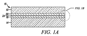
[0055]図1A及び1Bを参照すると、下記に記載するタイプの多層はんだ付け接続によってリードフレーム14に接続されているチップ12(即ち集積回路及び/又はマイクロプロセッサー)を含む、本発明による代表的な電子実装配置10の断面概要図が示されている。
[0055] Referring to FIGS. 1A and 1B, an exemplary embodiment according to the present invention includes a chip 12 (ie, an integrated circuit and / or microprocessor) connected to a
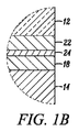
[0056]はんだ付け接続によってチップ12をリードフレーム構造体16に接続して図1Aに示す電子実装配置10を形成するダイ接続プロセスにおいて用いる前の本発明によるリードフレーム構造体16を、図2A及び2Bに示す。リードフレーム構造体16は、それに1以上のチップ(例えば図1Aのチップ12)を取り付けることができる金属製の導電性基材の形態のリードフレーム14を含み、リードフレーム14及び/又は取り付けられたチップにはまた、それに接続されている導線又は他の部品(図示せず)を含ませることもできる。リードフレーム14は、通常は純銅又は銅合金から製造される。
[0056] A leadframe structure 16 according to the present invention prior to use in a die connection process to connect the
[0057]しかしながら、リードフレーム14が純銅又は銅合金から製造されている場合には、リードフレーム14の銅の表面は、大気中の酸素と接触することによって自発的に酸化銅に酸化して、それによって酸化銅層を形成する傾向がある。酸化銅は電気絶縁性であり、リードフレーム14の導電性を劣化させる可能性があり、形成される酸化銅層はまた、ダイ接続プロセス中に液体のはんだがリードフレーム14の表面を濡らす能力を妨げる可能性があり、及び/又はリードフレーム14とチップ12の間に形成される接続の強度を弱める可能性がある。
[0057] However, if the
[0058]リードフレーム14には、下層のリードフレーム14の金属の酸化を阻止するために、用途に応じてリードフレーム14の少なくとも1つの表面上、及び場合によってはリードフレーム14の対向する表面のそれぞれの上に金属バリヤ層18が与えられる。バリヤ層18は、リードフレーム14の金属と比べて減少した酸化傾向を有する金属で形成することができる。一態様においては、バリヤ層18は純ニッケル又はニッケル合金から形成される。而して、バリヤ層18は、リードフレーム14の表面を覆って、リードフレーム14の金属が周囲環境と接触して、自発的に酸素によって酸化するのを阻止する。更に、下記において議論するように、バリヤ層18はまた、ダイ接続プロセス中にリードフレーム14の金属がチップ12をリードフレーム14に固定するために用いるはんだと接触して、リードフレーム14の金属とはんだの1種類又は複数の金属の間で金属間化合物が形成されるのを阻止するようにも機能する。
[0058] The
[0059]バリヤ層18は、電気メッキ又は無電解メッキなどによるメッキプロセスによってリードフレーム14上に形成することができる。更に、バリヤ層18は、リードフレーム14の全表面の上に連続的又は一面に形成することができ、或いはリードフレーム14の表面のダイパッド領域及び/又は他の選択された領域の上に選択的に形成することができる。
[0059] The
[0060]電気メッキプロセスにおいては、リードフレーム14は、析出させる溶解金属の溶液の電気メッキ浴中のカソードである。析出させる金属は、通常はアノードである。電流を印加すると、浴中の溶解金属イオンが還元されてリードフレームカソード上に析出してバリヤ層18が形成される。
[0060] In the electroplating process, the
[0061]一態様においては、スルファミン酸塩電解液浴に溶解ニッケルを含ませることができ、電気メッキ浴はまた、通常は例えば光沢剤の形態で存在する有機添加剤は含まないようにすることもできる。上記の浴を使用することによって、多少粗いか、又は「艶消し」の仕上げ面を有する析出金属表面を得ることができる。 [0061] In one embodiment, the sulfamate electrolyte bath can include dissolved nickel, and the electroplating bath is also free of organic additives that are typically present, for example, in the form of brighteners. You can also. By using the above bath, it is possible to obtain a deposited metal surface that is somewhat rough or has a “matt” finish.
[0062]或いは、印加電流の存在下では行わず、それよりは水和次亜リン酸ナトリウム(NaPO2H2・H2O)のような還元剤を用いて、溶液から析出金属のイオンを還元して、金属をリードフレーム14の表面上に析出させる自触媒反応である無電解析出プロセスを用いることができる。かかるプロセスにしたがってリードフレーム上にメッキされたニッケルのバリヤ層は、「無電解ニッケル」層と呼ぶことができ、通常は例えば約2〜4重量%のリンと合金化されたニッケルを含むニッケル合金になる。
[0062] Alternatively, it is not performed in the presence of an applied current, but rather than using a reducing agent such as hydrated sodium hypophosphite (NaPO 2 H 2 .H 2 O), ions of the deposited metal are removed from the solution. An electroless deposition process, which is an autocatalytic reaction that reduces and deposits metal on the surface of the
[0063]通常は、バリヤ層18の厚さは、10ミクロン(μm)以下、例えば1μm〜10μmの間である。一態様においては、バリヤ層18の厚さは、例えば、1、2、又は3μmのように薄く、5、6、7、8、9、又は10μmのように厚くてよく、或いは上記の値の任意の対の間で規定される任意の範囲内の厚さを有していてよい。例えば、バリヤ層18の厚さは、約2〜約9μmの間;約2〜約8μmの間;約2〜約7μmの間;約2〜約6μmの間;約2〜約5μmの間;約3〜約9μmの間;約3〜約8μmの間;約3〜約7μmの間;約3〜約6μmの間;又は約3〜約5μmの間;であってよい。
[0063] Typically, the thickness of the
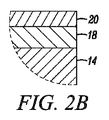
[0064]図2A及び2Bを参照すると、リードフレーム構造体16は、或いは濡れ促進性「フラッシュ」と呼ぶこともでき、下記において議論する理由のためにバリヤ層18と比べて相対的に薄くてよい濡れ促進層20を含む。濡れ促進層20は、ダイ接続プロセス中に液体はんだをリードフレーム14上に流動させる際に液体はんだがリードフレーム14全体を均一に濡らすことを助けるために、バリヤ層18上に形成する。
[0064] Referring to FIGS. 2A and 2B, the leadframe structure 16 may alternatively be referred to as a wetting-promoting “flash” and is relatively thin compared to the
[0065]濡れ促進層20は銅又は銅合金層であってよいが、或いは亜鉛、ビスマス、スズ、又はインジウム、並びに上記の合金の層であってもよい。特に、幾つかのはんだ組成物、特に上記に開示したタイプの亜鉛系はんだ組成物は、銅又は銅合金表面を非常に均一且つ有効に濡らすことが見出された。所望の場合には、リードフレーム構造体16は、濡れ促進層20の酸化を阻止するために、ダイ接続プロセスにおいて用いる前に不活性雰囲気中で実装することができる。はんだの濡れの促進に加えて酸化抵抗が所望の場合には、層20は、或いは金、白金、パラジウム、ルテニウム、又は銀の層であってもよい。
[0065] The wetting
[0066]濡れ促進層20は、10ミクロン(μm)以下、例えば1μm〜10μmの間の厚さを有していてよい。一態様においては、銅層16の厚さは、例えば、1、2、又は3μmのように薄く、5、6、7、8、9、又は10μmのように厚くてよく、或いは上記の値の任意の対の間で規定される任意の範囲内の厚さを有していてよい。例えば、濡れ促進層20の厚さは、約2μm〜約9μmの間;約2μm〜約8μmの間;約2μm〜約7μmの間;約2μm〜約6μmの間;約2μm〜約5μmの間;約3μm〜約9μmの間;約3μm〜約8μmの間;約3μm〜約7μmの間;約3μm〜約6μmの間;又は約3μm〜約5μmの間;であってよい。
[0066] The wetting
[0067]バリヤ層18をリードフレーム14上に形成する方法と同様に、濡れ促進層20は、例えば電解メッキ又は無電解メッキプロセスによってバリヤ層18上に析出させることができ、また、リードフレーム及び/又はバリヤ層全体の上に連続的又は一面に析出させることもでき、或いはリードフレーム及び/又はバリヤ層の表面のダイパッド領域及び/又は他の選択された領域のみの上に析出させることができる。
[0067] Similar to the method of forming the
[0068]図1A及び1Bに戻って、上記に開示したタイプの鉛フリーの亜鉛系はんだ組成物は、本実装配置において、チップ12をリードフレーム14に接続させるために用いるはんだ層22のために有利に用いることができる。はんだ層22において用いるための他の好適な亜鉛系はんだ組成物は、上記の本明細書中に包含した米国特許出願13/586,074において開示されている。
[0068] Returning to FIGS. 1A and 1B, a lead-free zinc-based solder composition of the type disclosed above is used for the
[0069]本発明者らは、液体の亜鉛系はんだを銅リードフレームに直接適用することの欠点は、ダイ接続プロセス中に亜鉛系はんだが銅リードフレームの表面を均一に濡らすが、液体の流動可能な亜鉛系はんだの上昇した液相温度(通常は、亜鉛系はんだに関しては330℃より高い)によって、比較的脆性で、亜鉛系はんだを固化させることによってCu/Zn金属間層又は銅リードフレームと亜鉛系はんだの間の界面が形成される際に通常は現れる銅/亜鉛(Cu/Zn)金属間化合物が形成されることであることを見出した。金属間層は、液体の亜鉛系はんだを銅リードフレームに直接適用する場合には比較的厚い可能性がある。 [0069] The inventors have the disadvantage of applying liquid zinc-based solder directly to the copper lead frame because the zinc-based solder wets the surface of the copper lead frame evenly during the die attach process. Cu / Zn intermetallic layers or copper leadframes that are relatively brittle due to the elevated liquidus temperature of possible zinc-based solders (usually higher than 330 ° C. for zinc-based solders) by solidifying the zinc-based solder It has been found that a copper / zinc (Cu / Zn) intermetallic compound that normally appears when the interface between the solder and the zinc-based solder is formed. The intermetallic layer can be relatively thick when liquid zinc-based solder is applied directly to a copper lead frame.
[0070]更に、例えば実装配置の製造後であって、電子実装配置を約150℃より高い温度のような高温に曝露する用途において使用中においては、更なるCu/Zn金属間化合物が形成される可能性があり、このようにしてCu/Zn金属間層又は界面の厚さが時間経過と共に増加する可能性がある。多くの電子実装構成において、特に例えば25mm2より大きいチップ−リードフレーム接続を有する「大型フレーム」用途においては、Cu/Zn金属間層の厚さは望ましくない厚さを有する可能性があり、或いは使用中に最終的に望ましくない厚さに増加する可能性があり、これによって潜在的にチップとリードフレームの間の接続が比較的脆性の金属間層を横切って欠落するダイクラックの事象が引き起こされる。更に、亜鉛系はんだの比較的高い弾性率は、上記の接続に少ししか応力緩和を与えない傾向がある。 [0070] Further, additional Cu / Zn intermetallic compounds are formed during use in applications where, for example, the mounting arrangement is manufactured and the electronic mounting arrangement is exposed to high temperatures, such as temperatures above about 150 ° C. In this way, the thickness of the Cu / Zn intermetallic layer or interface may increase over time. In many electronic packaging configurations, particularly in “large frame” applications with chip-leadframe connections greater than 25 mm 2 , the thickness of the Cu / Zn intermetallic layer may have an undesirable thickness, or In use, it can eventually increase to an undesirable thickness, which potentially causes a die crack event where the connection between the chip and the leadframe is missing across the relatively brittle intermetallic layer. It is. Furthermore, the relatively high modulus of elasticity of zinc-based solder tends to provide little stress relaxation to the above connection.
[0071]更に、亜鉛系はんだは、上記で議論したように下層のリードフレームを酸化から保護するために与えられるニッケルのような金属バリヤ層上を僅かしか濡らさない傾向がある。 [0071] In addition, zinc-based solders tend to wet slightly on a metal barrier layer such as nickel that is provided to protect the underlying leadframe from oxidation as discussed above.
[0072]しかしながら、ここに開示する本実装配置10において与えられている濡れ促進層20は比較的薄く、下記において議論する理由のために濡れを誘発させる犠牲層とみなすことができる。例えば、銅又は銅合金から形成される場合には、濡れ促進層20は、まず曝露された銅層又は表面を与えて、ダイ接続プロセス中に流動適用することによって亜鉛系はんだの均一な濡れを促進し、更に亜鉛系はんだ中の亜鉛と実質的に完全に反応して、図1A及び1Bに示されるように、バリヤ層18とはんだ層22の間に薄い特定目的のCu/Zn金属間層24又は界面を形成する。特定目的のCu/Zn金属間層24は、銅濡れ促進層20中に当初に存在する銅の実質的に全部が消費されることによって形成され、これにより比較的薄く、ダイ接続プロセスにおけるはんだ流動中に銅濡れ促進層20中の銅の実質的に全部がはんだ層22中の亜鉛と結合して金属間層24を形成するという事実のために電子実装配置の使用中に増加する可能性を有しないCu/Zn金属間層24が形成される。また、特定目的のCu/Zn金属間層24は十分に薄くて、かかる層内の亀裂破損の可能性が大きく減少し、これにより実装構造体10のために好ましい耐久性がもたらされる。
[0072] However, the wetting promoting
[0073]特定目的のCu/Zn金属間層24は、3μm〜10μmの間のような10ミクロン(μm)以下の厚さを有していてよい。一態様においては、銅層16の厚さは、例えば、3、4、又は5μmのように薄く、5、6、7、8、9、又は10μmのように厚くてよく、或いは上記の値の任意の対の間で規定される任意の範囲内の厚さを有していてよい。例えば、銅層16の厚さは、約4μm〜約9μmの間;約4μm〜約8μmの間;約4μm〜約7μmの間;約4μm〜約6μmの間;約4μm〜約5μmの間;約5μm〜約9μmの間;約5μm〜約8μmの間;約5μm〜約7μmの間;又は約5μm〜約6μmの間;であってよい。
[0073] The special purpose Cu /
[0074]本発明を好ましいデザインを有するものとして記載したが、本発明は発明の精神及び範囲内で更に修正することができる。したがって、本出願は、その一般原理を用いる本発明の任意の変更、使用、又は適応をカバーすると意図される。更に、本出願は、本発明が属する技術における公知又は慣習的な手順に包含され、特許請求の範囲の限界内に包含される本発明からのかかる逸脱をカバーすると意図される。 [0074] While this invention has been described as having a preferred design, the present invention can be further modified within the spirit and scope of the invention. This application is therefore intended to cover any variations, uses, or adaptations of the invention using its general principles. Furthermore, this application is intended to cover such deviations from the invention which are encompassed within known or routine procedures in the art to which the invention belongs and which are within the scope of the claims.
[0075]以下の非限定的な実施例は本発明の種々の特性及び特徴を示すものであり、それに対する限定と解釈すべきではない。
実施例1:
はんだ組成物の製造及び分析:
I.試料の製造:
[0076]本実施例においては、下表6にしたがって、種々の量の亜鉛(Zn)、アルミニウム(Al)、ゲルマニウム(Ge)、ガリウム(Ga)、及びマグネシウム(Mg)を含む複数のはんだ合金試料を調製した。それぞれの試料は、材料を410℃の温度に加熱して溶融体を形成することによって調製した。次に、それぞれの溶融体を、窒素雰囲気中で成形して直径1インチのビレットを形成した。
[0075] The following non-limiting examples are illustrative of the various properties and features of the invention and should not be construed as limiting thereto.
Example 1:
Production and analysis of solder composition:
I. Sample manufacture:
[0076] In this example, a plurality of solder alloys comprising various amounts of zinc (Zn), aluminum (Al), germanium (Ge), gallium (Ga), and magnesium (Mg) according to Table 6 below. Samples were prepared. Each sample was prepared by heating the material to a temperature of 410 ° C. to form a melt. Each melt was then molded in a nitrogen atmosphere to form a 1 inch diameter billet.
II.押出し:
[0077]はんだビレットを、200〜300℃及び10,342〜13,790キロパスカル(1500〜2000ポンド/平方インチ(psi))においてダイを用いて押出して、約0.762mm(0.030インチ)の直径を有するはんだ線を形成した。次に、はんだ線を、51mm(2インチ)の直径の内側ハブ、及び102mm(4インチ)の直径を有する2つの外側フランジを有するスプール上に巻回した。
II. Extrusion:
[0077] The solder billet is extruded with a die at 200-300 ° C. and 10,342-13,790 kilopascals (1500-2000 pounds per square inch (psi)), and is approximately 0.062 inches (0.030 inches). ) Was formed. The solder wire was then wound onto a spool having a 51 mm (2 inch) diameter inner hub and two outer flanges having a diameter of 102 mm (4 inch).
[0078]押出の結果を下表7に示す。「合格」と印された試料は、2以上の片に破断することなく、成功裏に線に押出されて、スプール上に巻付けられた。「不合格」と印された試料は、非常に脆性であったので巻き付け線に形成することができなかった。 [0078] The results of extrusion are shown in Table 7 below. The sample marked “pass” was successfully extruded into a line and wound on a spool without breaking into two or more pieces. The sample marked “Fail” was so brittle that it could not be formed into a wrap.
III.溶融特性:
[0079]Perkin Elmer DSC7装置を用いる示差走査熱量測定(DSC)によって、試料はんだ線の溶融特性を求めた。この装置を用いて固相線温度及び液相線温度を測定した。融点範囲は、液相線温度と固相線温度の間の差として算出した。試料はんだ線の溶融特性を下表8に示す。
III. Melting characteristics:
[0079] The melting properties of the sample solder wires were determined by differential scanning calorimetry (DSC) using a Perkin Elmer DSC7 apparatus. Using this apparatus, the solidus temperature and the liquidus temperature were measured. The melting point range was calculated as the difference between the liquidus temperature and the solidus temperature. The melting characteristics of the sample solder wires are shown in Table 8 below.
IV.機械特性:
[0080] 試料はんだ線の伸びは、「金属材料の引張試験に関する標準的な試験方法」と題されたASTM−E8にしたがってInstron 4465装置を室温で運転することによって評価した。
IV. Mechanical properties:
[0080] The elongation of the sample solder wire was evaluated by operating the Instron 4465 apparatus at room temperature in accordance with ASTM-E8 entitled "Standard Test Method for Tensile Testing of Metallic Materials".
[0081]試料はんだ線の延性は、曲げ大角破損率(曲げBR−HA)試験を室温で行うことによって求めた。図3に、曲げBR−HA延性試験のための実験構成を示す。示されているように、スプール110は、平行なフランジ112、内側ハブ114、及びスロット116を含む。内側ハブ114は平行なフランジ112の間に位置して、その間に空間を形成している。内側ハブ114は51mmの直径を有し、フランジ112は102mmの直径を有する。内側ハブ114内にスロット116が形成されている。線118の一端をスロット116中に挿入し、線118を内側ハブ114上に巻回する。図3に示されているように、孔116内の線118の端部は、内側ハブ114内に巻回される線118と角度Aを形成しており、角度Aは90°より大きい。試験は、それぞれの線118が成功裏に曲がって、破断することなく空のスプール110のハブ114の周りに一回巻回されるかどうかを評価する。それぞれの試料に関して、曲げBR−HA延性試験の10回の実験を行った。
[0081] The ductility of the sample solder wire was determined by performing a bending large angle failure rate (bending BR-HA) test at room temperature. FIG. 3 shows an experimental configuration for the bending BR-HA ductility test. As shown, the spool 110 includes parallel flanges 112, an
[0082]試料はんだ線の機械特性を下表9に示す。曲げBR−HA延性試験に関しては、「合格」と印された試料は、10回の実験の少なくとも7回の間に破断することなく成功裏に曲がって巻回され、一方、「不合格」と印された試料は、10回の実験の少なくとも4回の間に破断した。 [0082] The mechanical properties of the sample solder wires are shown in Table 9 below. For the bending BR-HA ductility test, samples marked “pass” were successfully bent and wound without breaking during at least 7 out of 10 experiments, whereas “fail” The marked sample broke during at least 4 out of 10 experiments.
V.濡れ性:
[0083]試料はんだ線の濡れ性は、95体積%の窒素及び5体積%の水素を含むフォーミングガスを用いて、ASM-SD890Aダイボンダーを410℃で運転することによって求めた。はんだ線を高温の銅リードフレームに供給して、はんだ線を溶融させて、リードフレーム上にドットを形成した。
V. Wettability:
[0083] The wettability of the sample solder wire was determined by operating an ASM-SD890A die bonder at 410 ° C. using a forming gas containing 95% by volume nitrogen and 5% by volume hydrogen. The solder wire was supplied to a high-temperature copper lead frame, and the solder wire was melted to form dots on the lead frame.
[0084]「ドットサイズ」を評価するために、それぞれのドットの寸法を1〜5のスケールで測定した。ここで、1は小さいドット(即ち低い濡れ性)を表し、5は大きなドット(即ち高い濡れ性)を表す。 [0084] To evaluate "dot size", the dimensions of each dot were measured on a scale of 1-5. Here, 1 represents a small dot (that is, low wettability), and 5 represents a large dot (that is, high wettability).
[0085]「濡れパターン」を評価するために、それぞれのドットをプレス下に配置して約100グラムの荷重をかけた。それぞれのプレスしたドットの寸法を1〜5のスケールで測定した。ここで、1は小さい展開(即ち低い濡れ性)を表し、5は大きな展開(即ち高い濡れ性)を表す。 [0085] To evaluate the “wetting pattern”, each dot was placed under the press and a load of about 100 grams was applied. The dimensions of each pressed dot were measured on a scale of 1-5. Here, 1 represents a small development (ie low wettability) and 5 represents a large development (ie high wettability).
[0086]試料はんだ線の濡れ性を下表10に示す。 [0086] Table 10 shows the wettability of the sample solder wires.
VI.分析:
[0087]試料1は最も良好な総合的な性能−良好な押出性(表7)、伸び及び延性などの良好な機械特性(表9)、並びに良好な濡れ性(表10)−を示した。
VI. analysis:
[0087] Sample 1 exhibited the best overall performance-good extrudability (Table 7), good mechanical properties such as elongation and ductility (Table 9), and good wettability (Table 10). .
[0088]高いレベルのマグネシウムは、試料1と比べて濡れ性を向上させることなく、押出性及び延性に悪影響を与えることが示された。試料1は0.25重量%のマグネシウムを含んでいた。1重量%以上のマグネシウムを含んでいた試料10及び15〜17は、非常に脆性であったので押出線を形成することができなかった(表7)。0.5重量%以上のマグネシウムを含んでいた試料6及び14は、成功裏に押出された(表7)が、曲げBR−HA延性試験は不合格であった(表9)。試料6、10、及び14〜17のいずれも、試料1と比べて向上した濡れ性を示さなかった(表10)。
[0088] High levels of magnesium have been shown to adversely affect extrudability and ductility without improving wettability compared to Sample 1. Sample 1 contained 0.25 wt% magnesium.
[0089]低いレベルのマグネシウムも、試料1と比べて濡れ性を向上させなかった。ここでも、試料1は0.25重量%のマグネシウムを含んでいた。0.12重量%以下のマグネシウムを含んでいた試料8、9、及び11は、試料1よりも小さい濡れ性を示した(表10)。
[0089] Low levels of magnesium also did not improve wettability compared to Sample 1. Again, Sample 1 contained 0.25 wt% magnesium.
[0090]ガリウムの高いレベルは、試料1と比べて濡れ性を向上させることなく押出性及び延性に悪影響を与えることが示された。試料1は0.5重量%のガリウムを含んでいた。1重量%以上のガリウムを含んでいた試料10、15、16、及び18は、非常に脆性であったので押出線を形成することができなかった(表7)。これも1重量%以上のガリウムを含んでいた試料2及び14は、成功裏に押出された(表7)が、曲げBR−HA延性試験は不合格であった(表9)。試料2、10、14〜16、及び18のいずれも、試料1と比べて向上した濡れ性を示さなかった(表10)。
[0090] High levels of gallium have been shown to adversely affect extrudability and ductility without improving wettability compared to Sample 1. Sample 1 contained 0.5% by weight of gallium.
[0091]低いレベルのガリウムも、試料1と比べて濡れ性を向上させなかった。ここでも、試料1は0.5重量%のガリウムを含んでいた。0.05重量%のガリウムを含んでいた試料5及び11は、試料1よりも小さい濡れ性を示した(表10)。 [0091] Low levels of gallium also did not improve wettability compared to Sample 1. Again, Sample 1 contained 0.5 weight percent gallium. Samples 5 and 11, which contained 0.05% by weight gallium, showed less wettability than sample 1 (Table 10).
[0092]ゲルマニウムの高いレベル及び低いレベルも、試料1と比べて濡れ性を向上させなかった。試料1は5重量%のゲルマニウムを含んでいた。それぞれ8、2、及び0重量%のゲルマニウムを含んでいた試料12、13、及び14は、試料1よりも小さい濡れ性を示した(表10)。
[0092] High and low levels of germanium also did not improve wettability compared to Sample 1. Sample 1 contained 5% by weight germanium.
実施例2:
リードフレーム構造体の製造:
[0093]本実施例においては、本発明によるリードフレーム構造体を製造した。純銅リードフレームを入手し、無電解メッキプロセスを用いて純ニッケルを6μmの厚さまでメッキした。
Example 2:
Manufacture of lead frame structure:
[0093] In this example, a lead frame structure according to the present invention was manufactured. A pure copper lead frame was obtained and pure nickel was plated to a thickness of 6 μm using an electroless plating process.
[0094]銅の相対的に薄い層を、無電解メッキプロセスによってニッケル層の上に析出させた。
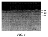
[0095]図4は、厚さ2μmの銅層を有する第1のリードフレーム構造体のSEM断面画像であり、図5は、厚さ8μmの銅層を有する第2のリードフレーム構造体のSEM断面画像である。それぞれのリードフレーム構造体は、銅リードフレーム200、ニッケルメッキ202、及び銅フラッシュ又は銅層204を含む。
[0094] A relatively thin layer of copper was deposited on the nickel layer by an electroless plating process.
[0095] FIG. 4 is a SEM cross-sectional image of a first lead frame structure having a 2 μm thick copper layer, and FIG. 5 is a SEM of a second lead frame structure having a 8 μm thick copper layer. It is a cross-sectional image. Each lead frame structure includes a
実施例3:
はんだの濡れ性の検討:
[0096]亜鉛系はんだ組成物をその液相線温度よりも高い温度に加熱し、ASM 890ダイボンダーを用いて図4及び5のリードフレーム上を濡らした。結果をそれぞれ図6及び7の画像において示す。図6及び7において示されるように、亜鉛系はんだはリードフレームの銅層を横切って均一に濡らし、2μm(図6)及び8μm(図7)の銅層を有するリードフレームの両方の上を広く被覆した。
Example 3:
Examination of solder wettability:
[0096] The zinc-based solder composition was heated to a temperature above its liquidus temperature and wetted on the lead frame of FIGS. 4 and 5 using an ASM 890 die bonder. The results are shown in the images of FIGS. 6 and 7, respectively. As shown in FIGS. 6 and 7, the zinc-based solder wets uniformly across the copper layer of the lead frame and spreads widely over both the lead frame with copper layers of 2 μm (FIG. 6) and 8 μm (FIG. 7). Covered.
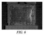
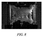
[0097]比較例においては、同じ亜鉛系はんだ組成物で、ニッケルバリヤ層を含んでいるが、上層の銅層を含んでいない対照リードフレーム上を濡らした。図8において示されるように、はんだの濡れは均一でなく、大きな面積の濡らしていないはんだが、一定体積のはんだを表すはんだボールと一緒に観察され、これははんだの流動中に主はんだ領域から分離し始めた。 [0097] In a comparative example, the same zinc-based solder composition was wetted on a control lead frame that contained a nickel barrier layer but no upper copper layer. As shown in FIG. 8, the solder wetting is not uniform, and a large area of non-wetting solder is observed along with solder balls representing a constant volume of solder, which from the main solder area during solder flow. Began to separate.
実施例4:
Cu/Zn金属間層の分析:
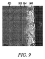
[0098]図9及び11は、リードフレーム上に亜鉛系はんだを流動させて固化させた後の、それぞれ図6及び7のリードフレームから撮ったSEM断面画像である。図10及び12は、材料のリードフレームの断面全体にわたって種々の深さで撮ったX線ラインスキャン元素分析結果である。
Example 4:
Analysis of the Cu / Zn intermetallic layer:
[0098] FIGS. 9 and 11 are SEM cross-sectional images taken from the lead frame of FIGS. 6 and 7, respectively, after the zinc-based solder is flowed and solidified on the lead frame. 10 and 12 are X-ray line scan elemental analysis results taken at various depths across the cross-section of the material leadframe.
[0099]図9及び10を参照すると、リードフレーム構造体は、2μmの銅層を有するリードフレームに関して、銅リードフレーム300、ニッケル層302、銅層304、銅/亜鉛金属間層306、及び亜鉛系はんだ308を含み、層中の銅の実質的に全部が亜鉛系はんだからの亜鉛と反応して約2μmの厚さを有するCu/Zn金属間層を形成しており、層中の銅は未反応の純銅としては実質的に残留していなかった。図10を参照すると、純ニッケルの別個の層、及びCu/Zn金属間層が形成されたことが分かる。
[0099] Referring to FIGS. 9 and 10, the leadframe structure relates to a leadframe having a 2 μm copper layer, a
[00100]図11及び12を参照すると、8μmの銅層を有するリードフレームに関して、銅層中の約4μmの深さまでの銅が亜鉛系はんだからの亜鉛と反応して、約4μmの厚さを有するCu/Zn金属間層を形成しており、元の銅層の純銅の約4μmが純粋で未反応の状態のままであった。図12を参照すると、純ニッケル及び純銅の別個の層、並びにCu/Zn金属間層が形成されたことが分かる。 [00100] Referring to FIGS. 11 and 12, for a lead frame having an 8 μm copper layer, copper up to a depth of about 4 μm in the copper layer reacts with zinc from a zinc-based solder to a thickness of about 4 μm. A Cu / Zn intermetallic layer having about 4 μm of pure copper of the original copper layer remained pure and unreacted. Referring to FIG. 12, it can be seen that separate layers of pure nickel and pure copper and a Cu / Zn intermetallic layer were formed.
[00101]本発明の範囲から逸脱することなく、議論した代表的な態様に対して種々の修正及び付加を行うことができる。例えば、上記に記載の態様は特定の特徴に関するものであるが、本発明の範囲はまた、記載されている特徴の全部は含んでいない複数の特徴及び態様の異なる組合せを有する態様も包含する。したがって、本発明の範囲は、特許請求の範囲及びその全ての等価物の範囲内に含まれる全てのかかる代替、修正、及び変更を包含すると意図される。 [00101] Various modifications and additions can be made to the exemplary aspects discussed without departing from the scope of the present invention. For example, although the aspects described above relate to particular features, the scope of the invention also encompasses embodiments having a plurality of features and different combinations of embodiments that do not include all of the described features. Accordingly, the scope of the invention is intended to embrace all such alternatives, modifications and variations that fall within the scope of the appended claims and all equivalents thereof.
[00101]本発明の範囲から逸脱することなく、議論した代表的な態様に対して種々の修正及び付加を行うことができる。例えば、上記に記載の態様は特定の特徴に関するものであるが、本発明の範囲はまた、記載されている特徴の全部は含んでいない複数の特徴及び態様の異なる組合せを有する態様も包含する。したがって、本発明の範囲は、特許請求の範囲及びその全ての等価物の範囲内に含まれる全てのかかる代替、修正、及び変更を包含すると意図される。
本発明の具体的態様は以下のとおりである。
[1]
約77〜約93重量%の亜鉛;
約3〜約15重量%のアルミニウム;
約3〜約7重量%のゲルマニウム;
約0.25〜約0.75重量%のガリウム;及び
約0.125〜約0.375重量%のマグネシウム;
を含むはんだ組成物。
[2]
約0.275〜約0.725重量%のガリウムを含む、[1]に記載のはんだ組成物。
[3]
約0.15〜約0.35重量%のマグネシウムを含む、[1]に記載のはんだ組成物。
[4]
約6重量%のアルミニウム;及び
約5重量%のゲルマニウム;
を含む、[1]に記載のはんだ組成物。
[5]
約0.001〜約2.5重量%のネオジムを含む、[1]に記載のはんだ組成物。
[6]
亜鉛、アルミニウム、ゲルマニウム、ガリウム、及びマグネシウムから構成される、[1]に記載のはんだ組成物。
[7]
88.25重量%の亜鉛;
6重量%のアルミニウム;
5重量%のゲルマニウム;
0.5重量%のガリウム;及び
0.25重量%のマグネシウム;
から構成される、[1]に記載のはんだ組成物。
[8]
はんだ組成物がマグネシウムよりも多いガリウムを含む、[1]に記載のはんだ組成物。
[9]
[1]に記載のはんだ組成物を含むはんだ線。
[10]
はんだ線が約1ミリメートル未満の直径を有する、[1]に記載のはんだ線。
[00101] Various modifications and additions can be made to the exemplary aspects discussed without departing from the scope of the present invention. For example, although the aspects described above relate to particular features, the scope of the invention also encompasses embodiments having a plurality of features and different combinations of embodiments that do not include all of the described features. Accordingly, the scope of the invention is intended to embrace all such alternatives, modifications and variations that fall within the scope of the appended claims and all equivalents thereof.
Specific embodiments of the present invention are as follows.
[1]
From about 77 to about 93 weight percent zinc;
About 3 to about 15 weight percent aluminum;
About 3 to about 7 weight percent germanium;
From about 0.25 to about 0.75% by weight of gallium; and
From about 0.125 to about 0.375 weight percent magnesium;
A solder composition comprising:
[2]
The solder composition according to [1], comprising about 0.275 to about 0.725% by weight of gallium.
[3]
The solder composition according to [1], comprising about 0.15 to about 0.35 wt% magnesium.
[4]
About 6% aluminum by weight; and
About 5% by weight of germanium;
The solder composition according to [1], comprising:
[5]
The solder composition according to [1], comprising about 0.001 to about 2.5% by weight of neodymium.
[6]
The solder composition according to [1], which is composed of zinc, aluminum, germanium, gallium, and magnesium.
[7]
88.25 wt% zinc;
6% aluminum by weight;
5% by weight germanium;
0.5% by weight of gallium; and
0.25 wt% magnesium;
The solder composition according to [1], comprising:
[8]
The solder composition according to [1], wherein the solder composition contains more gallium than magnesium.
[9]
A solder wire comprising the solder composition according to [1].
[10]
The solder wire of [1], wherein the solder wire has a diameter of less than about 1 millimeter.
Claims (10)
約3〜約15重量%のアルミニウム;
約3〜約7重量%のゲルマニウム;
約0.25〜約0.75重量%のガリウム;及び
約0.125〜約0.375重量%のマグネシウム;
を含むはんだ組成物。 From about 77 to about 93 weight percent zinc;
About 3 to about 15 weight percent aluminum;
About 3 to about 7 weight percent germanium;
From about 0.25 to about 0.75% by weight gallium; and from about 0.125 to about 0.375% by weight magnesium;
A solder composition comprising:
約5重量%のゲルマニウム;
を含む、請求項1に記載のはんだ組成物。 About 6 wt% aluminum; and about 5 wt% germanium;
The solder composition according to claim 1, comprising:
6重量%のアルミニウム;
5重量%のゲルマニウム;
0.5重量%のガリウム;及び
0.25重量%のマグネシウム;
から構成される、請求項1に記載のはんだ組成物。 88.25 wt% zinc;
6% aluminum by weight;
5% by weight germanium;
0.5 wt% gallium; and 0.25 wt% magnesium;
The solder composition according to claim 1, comprising:
Applications Claiming Priority (7)
| Application Number | Priority Date | Filing Date | Title |
|---|---|---|---|
| US201361911592P | 2013-12-04 | 2013-12-04 | |
| US61/911,592 | 2013-12-04 | ||
| US201461934161P | 2014-01-31 | 2014-01-31 | |
| US61/934,161 | 2014-01-31 | ||
| US14/554,126 | 2014-11-26 | ||
| US14/554,126 US20150151387A1 (en) | 2013-12-04 | 2014-11-26 | Zinc-based lead-free solder compositions |
| PCT/US2014/067913 WO2015084723A1 (en) | 2013-12-04 | 2014-12-01 | Zinc-based lead-free solder compositions |
Publications (1)
| Publication Number | Publication Date |
|---|---|
| JP2017501879A true JP2017501879A (en) | 2017-01-19 |
Family
ID=53264251
Family Applications (1)
| Application Number | Title | Priority Date | Filing Date |
|---|---|---|---|
| JP2016536807A Pending JP2017501879A (en) | 2013-12-04 | 2014-12-01 | Zinc-based lead-free solder composition |
Country Status (7)
| Country | Link |
|---|---|
| US (1) | US20150151387A1 (en) |
| EP (1) | EP3077151B1 (en) |
| JP (1) | JP2017501879A (en) |
| KR (1) | KR20160093026A (en) |
| CN (1) | CN105764645B (en) |
| TW (1) | TWI645048B (en) |
| WO (1) | WO2015084723A1 (en) |
Cited By (2)
| Publication number | Priority date | Publication date | Assignee | Title |
|---|---|---|---|---|
| JP2018087331A (en) * | 2015-02-25 | 2018-06-07 | 富士フイルム株式会社 | Water dispersion of gel particles, method of producing the same, and image forming method |
| WO2018198455A1 (en) * | 2017-04-28 | 2018-11-01 | 三菱電機株式会社 | Junction structure, method for manufacturing same, electric motor, and method for manufacturing same |
Families Citing this family (8)
| Publication number | Priority date | Publication date | Assignee | Title |
|---|---|---|---|---|
| US9735126B2 (en) * | 2011-06-07 | 2017-08-15 | Infineon Technologies Ag | Solder alloys and arrangements |
| WO2014179108A1 (en) | 2013-05-03 | 2014-11-06 | Honeywell International Inc. | Lead frame construct for lead-free solder connections |
| WO2016161339A1 (en) * | 2015-04-03 | 2016-10-06 | Intel Corporation | Zn doped solders on cu surface finish for thin fli application |
| CN105643142A (en) * | 2016-04-08 | 2016-06-08 | 苏州捷德瑞精密机械有限公司 | Arc welding electrode additive and preparation method thereof |
| CN111230357B (en) * | 2020-03-23 | 2021-09-14 | 东北石油大学 | Zn-based amorphous brazing filler metal foil for aluminum alloy and preparation method thereof |
| CN111545948B (en) * | 2020-05-18 | 2021-12-07 | 河南机电职业学院 | Brazing alloy, brazing filler metal, preparation method and application of brazing filler metal and prepared brazing product |
| CN114769935B (en) * | 2022-04-13 | 2023-05-16 | 广州汉源微电子封装材料有限公司 | Lead-free solder and preparation method and application thereof |
| CN114789308B (en) * | 2022-04-18 | 2024-05-07 | 金华市双环钎焊材料有限公司 | Rare earth element-containing high-performance seamless flux-cored wire for copper and aluminum and manufacturing method thereof |
Citations (6)
| Publication number | Priority date | Publication date | Assignee | Title |
|---|---|---|---|---|
| JPS53124072A (en) * | 1977-04-05 | 1978-10-30 | Nec Corp | Semiconductor device |
| JPH1177291A (en) * | 1997-09-11 | 1999-03-23 | Showa Alum Corp | Low-temperature brazing method for aluminum die cast material |
| JP2000208533A (en) * | 1999-01-14 | 2000-07-28 | Sumitomo Metal Mining Co Ltd | Die bonding zn alloy |
| JP2011251332A (en) * | 2010-06-04 | 2011-12-15 | Sumitomo Metal Mining Co Ltd | HIGH-TEMPERATURE Pb-FREE SOLDER PASTE USING Al POWDER |
| JP2012183558A (en) * | 2011-03-07 | 2012-09-27 | Nihon Superior Co Ltd | Lead-free solder alloy and solder joint using the same |
| US20130045131A1 (en) * | 2011-08-17 | 2013-02-21 | Honeywell International Inc. | Lead-Free Solder Compositions |
Family Cites Families (11)
| Publication number | Priority date | Publication date | Assignee | Title |
|---|---|---|---|---|
| FR2271898B1 (en) * | 1974-05-22 | 1977-03-11 | Arbed | |
| EP0704272B1 (en) * | 1994-09-30 | 2002-01-09 | AT&T Corp. | Lead-free alloys for use in solder bonding |
| JP3343498B2 (en) * | 1997-06-13 | 2002-11-11 | 昭和電工株式会社 | Low temperature brazing filler metal |
| JPH11172353A (en) * | 1997-12-04 | 1999-06-29 | Sumitomo Metal Mining Co Ltd | Zn alloy for high temperature soldering |
| JP2001127076A (en) * | 1999-10-25 | 2001-05-11 | Sumitomo Metal Mining Co Ltd | Alloy member for die bonding |
| JP3800977B2 (en) * | 2001-04-11 | 2006-07-26 | 株式会社日立製作所 | Products using Zn-Al solder |
| JP2004082134A (en) * | 2002-08-23 | 2004-03-18 | Nippon Metal Ind Co Ltd | Tin-zinc based lead-free solder alloy and its mixture |
| JP4818641B2 (en) * | 2005-05-18 | 2011-11-16 | 内橋エステック株式会社 | Fuse element |
| US7749340B2 (en) * | 2005-10-24 | 2010-07-06 | Indium Corporation Of America | Technique for increasing the compliance of lead-free solders containing silver |
| JP5672132B2 (en) * | 2011-04-27 | 2015-02-18 | 住友金属鉱山株式会社 | Pb-free solder alloy mainly composed of Zn and method for producing the same |
| US9735126B2 (en) * | 2011-06-07 | 2017-08-15 | Infineon Technologies Ag | Solder alloys and arrangements |
-
2014
- 2014-11-26 US US14/554,126 patent/US20150151387A1/en not_active Abandoned
- 2014-12-01 CN CN201480065983.5A patent/CN105764645B/en active Active
- 2014-12-01 WO PCT/US2014/067913 patent/WO2015084723A1/en active Application Filing
- 2014-12-01 JP JP2016536807A patent/JP2017501879A/en active Pending
- 2014-12-01 KR KR1020167016239A patent/KR20160093026A/en not_active Application Discontinuation
- 2014-12-01 EP EP14867035.9A patent/EP3077151B1/en active Active
- 2014-12-03 TW TW103141999A patent/TWI645048B/en active
Patent Citations (6)
| Publication number | Priority date | Publication date | Assignee | Title |
|---|---|---|---|---|
| JPS53124072A (en) * | 1977-04-05 | 1978-10-30 | Nec Corp | Semiconductor device |
| JPH1177291A (en) * | 1997-09-11 | 1999-03-23 | Showa Alum Corp | Low-temperature brazing method for aluminum die cast material |
| JP2000208533A (en) * | 1999-01-14 | 2000-07-28 | Sumitomo Metal Mining Co Ltd | Die bonding zn alloy |
| JP2011251332A (en) * | 2010-06-04 | 2011-12-15 | Sumitomo Metal Mining Co Ltd | HIGH-TEMPERATURE Pb-FREE SOLDER PASTE USING Al POWDER |
| JP2012183558A (en) * | 2011-03-07 | 2012-09-27 | Nihon Superior Co Ltd | Lead-free solder alloy and solder joint using the same |
| US20130045131A1 (en) * | 2011-08-17 | 2013-02-21 | Honeywell International Inc. | Lead-Free Solder Compositions |
Cited By (5)
| Publication number | Priority date | Publication date | Assignee | Title |
|---|---|---|---|---|
| JP2018087331A (en) * | 2015-02-25 | 2018-06-07 | 富士フイルム株式会社 | Water dispersion of gel particles, method of producing the same, and image forming method |
| WO2018198455A1 (en) * | 2017-04-28 | 2018-11-01 | 三菱電機株式会社 | Junction structure, method for manufacturing same, electric motor, and method for manufacturing same |
| JP6440908B1 (en) * | 2017-04-28 | 2018-12-19 | 三菱電機株式会社 | Junction structure, manufacturing method thereof, electric motor, and manufacturing method thereof |
| EP3616827A4 (en) * | 2017-04-28 | 2020-09-02 | Mitsubishi Electric Corporation | Junction structure, method for manufacturing same, electric motor, and method for manufacturing same |
| US11059133B2 (en) | 2017-04-28 | 2021-07-13 | Mitsubishi Electric Corporation | Bonded structure, method of manufacturing same, electric motor, and method of manufacturing same |
Also Published As
| Publication number | Publication date |
|---|---|
| TWI645048B (en) | 2018-12-21 |
| CN105764645B (en) | 2019-03-12 |
| EP3077151A1 (en) | 2016-10-12 |
| KR20160093026A (en) | 2016-08-05 |
| EP3077151B1 (en) | 2019-02-20 |
| EP3077151A4 (en) | 2017-09-27 |
| CN105764645A (en) | 2016-07-13 |
| WO2015084723A1 (en) | 2015-06-11 |
| TW201536927A (en) | 2015-10-01 |
| US20150151387A1 (en) | 2015-06-04 |
Similar Documents
| Publication | Publication Date | Title |
|---|---|---|
| TWI645048B (en) | Zinc-based lead-free solder compositions | |
| US20210167034A1 (en) | Chip arrangements | |
| EP2883649B1 (en) | High-temperature lead-free solder alloy | |
| TWI618798B (en) | Lead-free solder alloy | |
| EP2589459B1 (en) | Bi-Sn-BASED HIGH-TEMPERATURE SOLDER ALLOY | |
| JP2009057630A (en) | Sn-PLATED CONDUCTIVE MATERIAL, METHOD FOR PRODUCING THE SAME, AND ELECTRICITY CARRYING COMPONENT | |
| JPWO2013132954A1 (en) | Bonding method, bonded structure and manufacturing method thereof | |
| EP3031566A1 (en) | Lead-free solder alloy | |
| JP2011143442A (en) | Power module having highly reliable solder-bonded part | |
| JP4115979B2 (en) | Lead-free solder material | |
| JP3878978B2 (en) | Lead-free solder and lead-free fittings | |
| US9520347B2 (en) | Lead frame construct for lead-free solder connections | |
| TWI272152B (en) | Doped alloys for electrical interconnects, methods of production and uses thereof | |
| EP2974818B1 (en) | Solder joining method | |
| KR102579479B1 (en) | Connecting Pin | |
| KR102579478B1 (en) | Metal pin for conductive connection | |
| JP5655714B2 (en) | Semiconductor device using Bi solder | |
| KR20240033887A (en) | Connecting method of pin | |
| KR20240033889A (en) | Connecting Pin | |
| KR20240033886A (en) | Transferring catridge for connecting pin | |
| JP2017136627A (en) | Pb-FREE In-BASED SOLDER ALLOY |
Legal Events
| Date | Code | Title | Description |
|---|---|---|---|
| A521 | Request for written amendment filed |
Free format text: JAPANESE INTERMEDIATE CODE: A523 Effective date: 20160809 |
|
| A621 | Written request for application examination |
Free format text: JAPANESE INTERMEDIATE CODE: A621 Effective date: 20171124 |
|
| A977 | Report on retrieval |
Free format text: JAPANESE INTERMEDIATE CODE: A971007 Effective date: 20181105 |
|
| A131 | Notification of reasons for refusal |
Free format text: JAPANESE INTERMEDIATE CODE: A131 Effective date: 20181119 |
|
| A601 | Written request for extension of time |
Free format text: JAPANESE INTERMEDIATE CODE: A601 Effective date: 20190219 |
|
| A521 | Request for written amendment filed |
Free format text: JAPANESE INTERMEDIATE CODE: A523 Effective date: 20190419 |
|
| A131 | Notification of reasons for refusal |
Free format text: JAPANESE INTERMEDIATE CODE: A131 Effective date: 20191001 |
|
| A02 | Decision of refusal |
Free format text: JAPANESE INTERMEDIATE CODE: A02 Effective date: 20200512 |