JP2017228564A - Wavelength tunable semiconductor laser array and method for controlling wavelength tunable semiconductor laser array - Google Patents
Wavelength tunable semiconductor laser array and method for controlling wavelength tunable semiconductor laser array Download PDFInfo
- Publication number
- JP2017228564A JP2017228564A JP2016121732A JP2016121732A JP2017228564A JP 2017228564 A JP2017228564 A JP 2017228564A JP 2016121732 A JP2016121732 A JP 2016121732A JP 2016121732 A JP2016121732 A JP 2016121732A JP 2017228564 A JP2017228564 A JP 2017228564A
- Authority
- JP
- Japan
- Prior art keywords
- semiconductor laser
- tunable semiconductor
- wavelength tunable
- wavelength
- layer
- Prior art date
- Legal status (The legal status is an assumption and is not a legal conclusion. Google has not performed a legal analysis and makes no representation as to the accuracy of the status listed.)
- Granted
Links
Images
Landscapes
- Semiconductor Lasers (AREA)
Abstract
【課題】波長切替動作を行う際に、温度変化が大きくなる活性層部分の影響を最小限に抑制する。【解決手段】光が導波する方向に活性層及び制御層がそれぞれ1つ以上並んだ構造を有する複数の波長可変半導体レーザが配列され、隣り合う波長可変半導体レーザはそれぞれ活性層と制御層の並びが逆である波長可変半導体レーザアレイにおいて、駆動させる波長可変半導体レーザを、第1の波長可変半導体レーザから第2の波長可変半導体レーザに切り替える際に、第1の波長可変半導体レーザの動作中に、第2の波長可変半導体レーザに隣り合う第3の波長可変半導体レーザ(及び第4の波長可変半導体レーザ)の制御層に電流を注入し、第2の波長可変半導体レーザが駆動すると同時に、第3(及び第4の)波長可変半導体レーザの制御層への電流注入を止める。【選択図】図2An object of the present invention is to minimize the influence of an active layer portion where a temperature change is large when performing a wavelength switching operation. A plurality of wavelength tunable semiconductor lasers having a structure in which one or more active layers and one or more control layers are arranged in a direction in which light is guided are arranged. Adjacent wavelength tunable semiconductor lasers are respectively formed of active layers and control layers. In the wavelength tunable semiconductor laser array having the reverse arrangement, when the wavelength tunable semiconductor laser to be driven is switched from the first tunable semiconductor laser to the second tunable semiconductor laser, the first tunable semiconductor laser is operating. In addition, current is injected into the control layer of the third wavelength tunable semiconductor laser (and the fourth wavelength tunable semiconductor laser) adjacent to the second wavelength tunable semiconductor laser, and at the same time as the second wavelength tunable semiconductor laser is driven, Stops current injection into the control layer of the third (and fourth) tunable semiconductor laser. [Selection] Figure 2
Description
本発明は、波長可変半導体レーザアレイ及び波長可変半導体レーザアレイの制御方法に関し、より詳細には、高速且つ高精度な波長切替が可能な波長可変半導体レーザアレイ及び波長可変半導体レーザアレイの制御方法に関する。 The present invention relates to a wavelength tunable semiconductor laser array and a method for controlling the wavelength tunable semiconductor laser array, and more particularly to a wavelength tunable semiconductor laser array capable of switching wavelengths at high speed and with high accuracy, and a method for controlling the wavelength tunable semiconductor laser array. .
近年のインターネットの普及に伴い、ネットワーク全体での通信トラフィックが飛躍的に増加しているため、光ファイバ通信の高速・大容量化が求められている。高速・大容量化の手段として、一本の光ファイバ内で複数の波長を用いることで伝送速度を向上させる波長分割多重(WDM)方式が有効である。WDM方式において、波長の一つ一つをチャネルといい、高速なチャネル(波長)切替を実現するために、高速高精度に波長を変化させることができる波長可変レーザが求められている。 With the spread of the Internet in recent years, the communication traffic in the entire network has increased dramatically, so that high-speed and large capacity optical fiber communication is required. As a means for increasing the speed and capacity, a wavelength division multiplexing (WDM) system that improves the transmission speed by using a plurality of wavelengths in one optical fiber is effective. In the WDM system, each wavelength is called a channel, and in order to realize high-speed channel (wavelength) switching, a tunable laser capable of changing the wavelength with high speed and high accuracy is required.
光ファイバ通信においては、単一の波長でレーザ発振する単一モードレーザというものが用いられている。単一モードレーザ発振を実現する方法としては、光導波路に周期的な凹凸の構造をした回折格子を用いるものがある。回折格子が形成された光導波路においては、光導波路の等価屈折率をn、前記回折格子の周期をΛとすると、その反射波長λBは以下の(1)式で表される。 In optical fiber communication, a single mode laser that oscillates at a single wavelength is used. As a method for realizing single mode laser oscillation, there is a method using a diffraction grating having a periodic uneven structure in an optical waveguide. In an optical waveguide in which a diffraction grating is formed, the reflection wavelength λ B is expressed by the following equation (1), where n is the equivalent refractive index of the optical waveguide and Λ is the period of the diffraction grating.
![]()
![]()
上記(1)式より、光導波路の等価屈折率を変化させることで反射波長を変化させることができることがわかる。つまり、回折格子を用いた光共振器を構成することで、選択的に波長を変化させられる波長可変レーザを構成することができる。回折格子を利用した波長可変レーザとしては、DBR(Distributed Bragg Reflector)レーザ、SG(Sampled Grating)-DBRレーザやSSG(Super Structure Grating)-DBRレーザなどがある。 From the above equation (1), it can be seen that the reflection wavelength can be changed by changing the equivalent refractive index of the optical waveguide. That is, by configuring an optical resonator using a diffraction grating, it is possible to configure a wavelength tunable laser that can selectively change the wavelength. Examples of wavelength tunable lasers using diffraction gratings include DBR (Distributed Bragg Reflector) lasers, SG (Sampled Grating) -DBR lasers, and SSG (Super Structure Grating) -DBR lasers.
波長可変分布活性(Tunable Distributed Amplification: TDA-)DFBレーザは、連続的に波長を変化させることのできる波長可変半導体レーザである。 The Tunable Distributed Amplification (TDA-) DFB laser is a wavelength tunable semiconductor laser capable of continuously changing the wavelength.
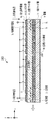
図1を参照してTDA-DFBレーザの基本的な構造を説明する。図1は、TDA-DFBレーザアレイに含まれるそれぞれ異なる発振波長帯を有する複数のTDA-DFBレーザのうちの1つのTDA-DFBレーザ100の導波路層の断面図である。TDA-DFBレーザは、下部クラッド層1と上部クラッド層4との間に、活性導波路層(本明細書において、活性層ともいう。)2と非活性導波路層(本明細書において、波長制御領域または制御層ともいう。)3とがそれぞれ一定の長さLa、Ltで交互に周期的に形成された構造になっている。下部クラッド層1には電極9が設けられ、上部クラッド層4にはコンタクト層6を介して制御層用電極7及び活性層用電極8が、非活性導波路層3及び活性導波路層2にそれぞれ対応するように設けられている。なお、図1に示すTDA-DFBレーザは、長さLa1の活性導波路層21と長さLt1の非活性導波路層31とが交互に形成された第1のレーザ部と、長さLa2の活性導波路層22と長さLt2の非活性導波路層32とが交互に形成された第2のレーザ部とが、位相シフト領域10を介して光の伝搬方向(活性導波路層と非活性導波路層の繰り返し方向(x方向))に直列に接続された構成例を示している(例えば、特許文献1参照)。しかしながら、必ずしも、1つのTDA-DFBレーザに複数のレーザ部を設ける必要はない。
The basic structure of the TDA-DFB laser will be described with reference to FIG. FIG. 1 is a cross-sectional view of a waveguide layer of one TDA-
活性導波路層2と非活性導波路層3の上部には、回折格子5が形成されており、回折格子の周期に応じた波長のみ選択的に反射されるようになっている。このTDA-DFBレーザにおいては、活性導波路層2に対応して設けられた活性層用電極8へ活性層電流Iaを注入することで、利得が生じ、前記回折格子で選択的に反射された波長においてレーザ発振が起こる。一方、非活性導波路層3に対応して設けられた制御用電極7へ制御層電流Itを注入すると、キャリアプラズマ効果により導波路内の屈折率変化が生じ、非活性導波路における回折格子の反射波長が変化する。非活性導波路層に注入する電流量を変化させることで、TDA-DFBレーザの発振波長を変化させることができる(例えば、特許文献1、2参照)。 A diffraction grating 5 is formed on the active waveguide layer 2 and the inactive waveguide layer 3 so that only a wavelength corresponding to the period of the diffraction grating is selectively reflected. In this TDA-DFB laser, the active layer current Ia is injected into the active layer electrode 8 provided corresponding to the active waveguide layer 2, thereby gain is generated and selectively reflected by the diffraction grating. Laser oscillation occurs at the wavelength. On the other hand, when the control layer current It is injected into the control electrode 7 provided corresponding to the inactive waveguide layer 3, the refractive index in the waveguide is changed by the carrier plasma effect, and the diffraction grating in the inactive waveguide is changed. The reflection wavelength changes. By changing the amount of current injected into the inactive waveguide layer, the oscillation wavelength of the TDA-DFB laser can be changed (see, for example, Patent Documents 1 and 2).
プラズマ効果を用いた波長変化は非常に高速で、その応答速度はns(10-9秒)オーダである。しかしながら、半導体素子に電流を注入することで抵抗成分のために熱が生じる。温度変化により、ms(10-3秒)オーダでゆっくりと波長が変化するという熱ドリフト現象が起きる。このように、波長変化の応答速度は波長の熱ドリフトの影響により律速されてしまう。 The wavelength change using the plasma effect is very fast, and the response speed is on the order of ns (10 -9 seconds). However, when current is injected into the semiconductor element, heat is generated due to the resistance component. Due to the temperature change, a thermal drift phenomenon occurs in which the wavelength slowly changes in the order of ms (10 -3 seconds). Thus, the response speed of the wavelength change is limited by the influence of the thermal drift of the wavelength.
この問題を解決するための技術がいくつか提案されている(例えば、特許文献2、3、4参照)。例えば、特許文献2、3では、波長可変半導体レーザにおいて、隣接する半導体レーザ(LD)を熱補償機構として用いて半導体素子全体の発熱量を制御することで上記熱ドリフトの抑制を行っている。 Several techniques for solving this problem have been proposed (see, for example, Patent Documents 2, 3, and 4). For example, in Patent Documents 2 and 3, in the wavelength tunable semiconductor laser, the thermal drift is suppressed by controlling the heat generation amount of the entire semiconductor element by using an adjacent semiconductor laser (LD) as a thermal compensation mechanism.
しかしながら、上述した熱ドリフトを抑制する手法は、動作中のTDA-DFBレーザに隣接した別のTDA-DFBレーザの制御層を熱補償機構として用いているが、TDA-DFBレーザアレイにおいて、同一LD内での波長切替動作ではなく、異なるLD間で波長切替動作を行う際に、最も電流変化が大きく発熱量が大きくなる活性層部分の熱を効率的に補償するために、構造の観点から検討されたものではない。 However, the above-described technique for suppressing thermal drift uses a control layer of another TDA-DFB laser adjacent to the operating TDA-DFB laser as a thermal compensation mechanism, but in the TDA-DFB laser array, the same LD In order to efficiently compensate for the heat of the active layer where the current change is the largest and the amount of heat generation is large when performing wavelength switching operation between different LDs instead of the wavelength switching operation in the inside, from the viewpoint of structure It is not what was done.
TDA-DFBレーザアレイを用いた波長切替動作においては、最も発熱量が大きく、熱ドリフトの影響が大きくなる、異なるLD間での切替動作時の温度変化を効率的に制御することが望ましい。 In the wavelength switching operation using the TDA-DFB laser array, it is desirable to efficiently control the temperature change during the switching operation between different LDs, which generates the largest amount of heat and is greatly affected by thermal drift.
本発明は、このような問題に鑑みてなされたもので、その目的とするところは、波長可変半導体アレイ(例えば、TDA-DFBレーザアレイ)において、動作中のLDを別のLDに切り替えて波長切替動作を行う際に最も電流変化量が大きくなる、すなわち、温度変化が大きくなる活性層部分の影響を最小限に抑制するよう、その構造を最適化した波長可変半導体レーザアレイ及び該波長可変半導体レーザアレイの制御方法を提供することにある。 The present invention has been made in view of such a problem, and an object of the present invention is to switch a wavelength of an operating LD to another LD in a wavelength tunable semiconductor array (for example, a TDA-DFB laser array). Wavelength tunable semiconductor laser array optimized for the structure and the wavelength tunable semiconductor so as to minimize the influence of the active layer portion where the amount of current change becomes the largest when switching operation is performed, that is, the temperature change is large It is to provide a method for controlling a laser array.
このような目的を達成するために、本願発明の第1の態様は、半導体基板内に光導波路が埋め込まれた構造の複数の半導体レーザを備えた波長可変半導体レーザアレイであって、複数の半導体レーザの各々は、光が導波する方向に配列された、活性層電流の注入により光利得を制御する活性層、及び制御電流の注入により導波する光に対する屈折率を変化させる制御層を含み、複数の半導体レーザのうちの隣り合う波長可変半導体レーザにおいて、一方の波長可変半導体レーザの活性層及び制御層は、他方の波長可変半導体レーザの制御層及び活性層とそれぞれ隣り合う位置に形成されている。 In order to achieve such an object, a first aspect of the present invention is a wavelength tunable semiconductor laser array including a plurality of semiconductor lasers having a structure in which an optical waveguide is embedded in a semiconductor substrate, the plurality of semiconductor lasers Each of the lasers includes an active layer that is arranged in a direction in which light is guided and that controls an optical gain by injection of an active layer current, and a control layer that changes a refractive index for the light guided by injection of a control current. In the adjacent wavelength tunable semiconductor lasers of the plurality of semiconductor lasers, the active layer and the control layer of one of the wavelength tunable semiconductor lasers are formed at positions adjacent to the control layer and the active layer of the other wavelength tunable semiconductor laser, respectively. ing.
本願発明の第2の態様は、上記波長可変半導体レーザアレイの制御方法であって、駆動させる波長可変半導体レーザを、第1の波長可変半導体レーザから第2の波長可変半導体レーザに切り替える際に、第1の波長可変半導体レーザの動作中に、第2の波長可変半導体レーザと隣り合う第3の波長可変半導体レーザの制御層に制御電流を注入することと、第2の波長可変半導体レーザが駆動するのと同時に、第3の波長可変半導体レーザ3の制御層への電流注入を止めることとを含む。 A second aspect of the present invention is a method for controlling the wavelength tunable semiconductor laser array, wherein the wavelength tunable semiconductor laser to be driven is switched from the first wavelength tunable semiconductor laser to the second wavelength tunable semiconductor laser. During the operation of the first wavelength tunable semiconductor laser, a control current is injected into the control layer of the third wavelength tunable semiconductor laser adjacent to the second wavelength tunable semiconductor laser, and the second wavelength tunable semiconductor laser is driven. And stopping the current injection into the control layer of the third wavelength tunable semiconductor laser 3 at the same time.
以上説明したように、本発明によれば、波長可変半導体アレイにおいて、動作中のLDを別のLDに切り替えて波長切替動作を行う際に温度変化が大きくなる活性層部分の影響を最小限に抑制する構造を有する波長可変半導体レーザアレイ及び該波長可変半導体レーザアレイの制御方法を提供することが可能となる。 As described above, according to the present invention, in the wavelength tunable semiconductor array, the influence of the active layer portion that causes a large temperature change when performing wavelength switching operation by switching the operating LD to another LD is minimized. It becomes possible to provide a wavelength tunable semiconductor laser array having a suppressing structure and a method for controlling the wavelength tunable semiconductor laser array.
本願発明は、波長可変半導体レーザアレイであって、電流注入により光利得を制御する導波路層(活性層)とコア層を導波する光に対する屈折率を変化させることができる導波路層(制御層)とが、光が導波する方向にそれぞれ1つ以上並んだ構造を有する波長可変半導体レーザが、2次元的(もしくは3次元的)に2つ以上配列され、隣り合う波長可変半導体レーザはそれぞれ活性層と制御層の並びが逆であることを特徴とする。 The present invention relates to a wavelength tunable semiconductor laser array, a waveguide layer (active layer) that controls optical gain by current injection, and a waveguide layer (control) that can change the refractive index for light guided through a core layer. Two or more wavelength tunable semiconductor lasers having a structure in which one or more layers are arranged in the direction in which light is guided, and two or more wavelength tunable semiconductor lasers are arranged two-dimensionally (or three-dimensionally). The arrangement of the active layer and the control layer is opposite, respectively.
また本願発明は、波長可変半導体レーザアレイの制御手法であって、駆動させる波長可変半導体レーザを、第1の波長可変半導体レーザから第2の波長可変半導体レーザに切り替える際に、第1の波長可変半導体レーザの動作中に、第2の波長可変半導体レーザに隣接する第3の波長可変半導体レーザ(及び第4の波長可変半導体レーザ)の制御層に電流を注入し、第2の波長可変半導体レーザが駆動すると同時に、第3(及び第4)の波長可変半導体レーザの制御層への電流注入を止めることを特徴とする。 The invention of the present application is a control method of the wavelength tunable semiconductor laser array, and the first wavelength tunable semiconductor laser is switched when the wavelength tunable semiconductor laser to be driven is switched from the first wavelength tunable semiconductor laser to the second wavelength tunable semiconductor laser. During the operation of the semiconductor laser, current is injected into the control layer of the third wavelength tunable semiconductor laser (and the fourth wavelength tunable semiconductor laser) adjacent to the second wavelength tunable semiconductor laser, and the second wavelength tunable semiconductor laser is injected. The current injection to the control layer of the third (and fourth) wavelength tunable semiconductor laser is stopped at the same time as is driven.
以下、図面を参照しながら本発明の実施形態について詳細に説明する。以下に説明する実施形態は本発明の実施例であり。本発明は、以下の実施形態に制限されるものではない。図面中の同一または類似の符号は同一または類似の要素を示す。
(実施形態1)
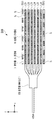
図2を参照して、本実施形態に係る半導体レーザアレイ(TDA-DFBレーザアレイ)200の構造及び制御方法について説明する。図2は、TDA-DFBレーザアレイの上面模式図である。TDA-DFBレーザアレイ200は、同一基板上に発振波長の異なる6個のTDA-DFBレーザ(LD1〜LD6)が、光の伝搬方向に垂直な方向(z方向)に一定の間隔(光のフィールドが重ならない程度の間隔)で並列に配置され、その出力光は合波器(例えばMMIカプラなど)202で合波された後、出力される。合波器202と各LDの出射端との間に光出力を増幅するために半導体光増幅器(Semiconductor Optical Amplifier:SOA)(不図示)を集積しても良い。TDA-DFBレーザアレイ200を構成する複数のTDA-DFBレーザは、同一基板上に2次元的または3次元的に配列される。
Hereinafter, embodiments of the present invention will be described in detail with reference to the drawings. The embodiments described below are examples of the present invention. The present invention is not limited to the following embodiments. The same or similar symbols in the drawings indicate the same or similar elements.
(Embodiment 1)
With reference to FIG. 2, the structure and control method of the semiconductor laser array (TDA-DFB laser array) 200 according to the present embodiment will be described. FIG. 2 is a schematic top view of the TDA-DFB laser array. In the TDA-
各LDは、図1に示したように、下部クラッド層1と上部クラッド層4との間に、活性層2と制御層3とがそれぞれ一定の長さで光の導波方向(x方向)に交互に周期的に配列された構造になっている。活性層2及び制御層3はそれぞれ一つの電極8、7に接続され、それぞれの電流値は単一電極で制御できるようになっている。各LDは、活性層2に電流(活性層電流)Iaを注入することでレーザ発振し、制御層3への注入電流(制御層電流)Itを制御することで、発振波長を変化させることができる。予め測定された制御層電流Itと発振波長の関係より、所望の発振波長が得られるように各電流値を設定する。 In each LD, as shown in FIG. 1, the active layer 2 and the control layer 3 have a fixed length between the lower cladding layer 1 and the upper cladding layer 4, respectively, and the optical waveguide direction (x direction). The structure is arranged periodically and alternately. The active layer 2 and the control layer 3 are respectively connected to one electrode 8 and 7, and each current value can be controlled by a single electrode. Each LD, by laser oscillation by injecting a current (active layer current) Ia to the active layer 2, to control the injection current (control layer current) I t to the control layer 3, changing the oscillation wavelength Can do. Than previously measured relationship between the control layer current I t oscillation wavelength, setting the current values as desired oscillation wavelength can be obtained.
本実施形態に係るTDA-DFBレーザアレイ200は、隣り合うLD同士の活性層2と制御層3の配列順序が逆になっている。図2に示すように、LD1、3、5は、出射端側から順に制御層3、活性層2、制御層3、活性層2・・・が形成されている。これに対して、LD1、3、5と隣り合うLD2、4、6は、出射端側から順に活性層2、制御層3、活性層2、制御層3・・・が形成されている。また、本実施形態に係るTDA-DFBレーザアレイ200は、LD1、LD6のさらに外側の隣り合う位置には、各LDと同じ構造を有するメサ(TDC1、2)が形成されている。LD1、LD6の外側の隣り合う位置のメサは、合波器202には接続されず、熱補償機構(TDC: Thermal Drift Compensator)として使用される。LD1とTDC1のz方向の間隔、及びLD6とTLD2のz方向の間隔は、隣り合うLD同士のz方向の間隔と同じである。熱補償機構として使用されるTDC1、2は、活性層2を含まなくてもよく、あるいは活性層2の代りに制御層3を配置してもよい。
In the TDA-
図2に示すように、あるLDの活性層2に着目すると、活性層2のz方向の隣り合う位置の一方または双方に、別のLDまたはTDCの制御層3が形成されている。
<動作方法>
上述したTDA-DFBレーザアレイ200を用いて高速且つ高精度な波長切替動作を行う方法について説明する。
As shown in FIG. 2, when attention is paid to the active layer 2 of a certain LD, another LD or TDC control layer 3 is formed at one or both of adjacent positions in the z direction of the active layer 2.
<Operation method>
A method for performing high-speed and high-accuracy wavelength switching operation using the above-described TDA-
ここでは、LD1に活性層電流Ia1及び制御層電流It1を注入して、LD1をλ1でレーザ発振させている状態(TDA-DFBレーザアレイ200の合波器202から、波長λ1のレーザが出射している状態)から、LD4に活性層電流Ia4及び制御相電流It4を注入し、LD4をλ2でレーザ発振させる状態に切り替えて、合波器202から出射する光の波長をλ1からλ2に変化させる場合を説明する。
Here, by injecting the active layer current Ia 1 and the control layer current I t1 to LD1, the multiplexer 202 of the laser oscillation is caused by that state (TDA-
LD4に活性層電流Ia4及び制御相電流It4を注入すると、LD4では、I4=Ia4+It4分の注入電流の変化に伴う熱ドリフトが発生し、切替時間の高速化が律速される。 When the active layer current Ia 4 and the control phase current It 4 are injected into the LD 4 , a thermal drift occurs in the LD 4 due to the change in the injection current of I 4 = Ia 4 + It 4 minutes, and the switching time is speeded up. The
ここで、LD1がλ1で動作している段階で、予めLD4の制御層にI4(=Ia4+It4)と同等の電流を注入することで、切替前後での電流量の変化をなくし、熱ドリフトを抑制することができる。すなわち、波長切替後にLD4の活性層2及び制御層3にそれぞれ注入される活性層電流Ia4及び制御相電流It4の合計と同等の電流(あるいは電力)を、波長切替前からLD4の制御層3に注入し予め熱を生じさせておくことで、波長切替時の熱ドリフトを抑制することができ、その結果、高速且つ高精度な波長切替動作を行うことができる。 Here, at the stage of operating in LD1 is lambda 1, previously I 4 (= Ia 4 + It 4) the control layer of LD4 and by injecting an equivalent current, the change in the current amount of before and after the switching And thermal drift can be suppressed. That is, the total equivalent of the current of the active layer current Ia 4 and the control phase current I t4 are respectively injected after wavelength switching the active layer 2 and the control layer 3 of LD4 (or power), the control layer of LD4 before wavelength switching By injecting into 3 and generating heat in advance, thermal drift during wavelength switching can be suppressed, and as a result, high-speed and highly accurate wavelength switching operation can be performed.
LD4の活性層2へ活性層電流Ia4を供給する際に発生する発熱も波長ドリフトに寄与する。したがって、LD4の活性層2へ供給する活性層電流Ia4は、活性層2の波長変化の時定数と同等もしくはそれよりも小さい時定数を有する波形の活性層電流Ia4を形成して注入することが望ましい。 The heat generated when the active layer current Ia 4 is supplied to the active layer 2 of the LD 4 also contributes to the wavelength drift. Therefore, the active layer current Ia 4 supplied to the active layer 2 of the LD 4 forms and injects the active layer current Ia 4 having a waveform having a time constant equal to or smaller than the time constant of the wavelength change of the active layer 2. It is desirable.
しかしながら、一般に、安定したレーザ発振を得るためには、活性層電流は制御層電流よりも大きくする。そのため、I4が大きくなりすぎた場合、波長切替前のLD4の制御層3への注入電流が過電流となり、素子を破損する可能性がある。 However, in general, in order to obtain stable laser oscillation, the active layer current is made larger than the control layer current. Therefore, if I 4 becomes too large, the injection current into the control layer 3 of the LD 4 before wavelength switching becomes an overcurrent, which may damage the element.
そこで、波長切替前に注入するI4を、LD4の制御層3と、LD4に隣接するLD5(もしくはLD3、もしくはその両方(LD3とLD5))の制御層3とに分配して注入することで、過電流による素子の破損を防ぐことができる。波長切替前に注入するI4の分配先を、LD4の制御層3を除く、LD4に隣接するLD5(もしくはLD3、もしくはその両方(LD3とLD5))の制御層3としてもよい。ここで、隣り合うTDA-DFBレーザ同士の活性層2と制御層3の配列順序が逆になっているので、配列順序が同じである場合よりも、波長切替後に最も電流変化が大きいLD4の活性層部2の発熱量の変化を、効率的に補償することができる。 Therefore, I 4 injected before wavelength switching is distributed and injected into the control layer 3 of LD4 and the control layer 3 of LD5 (or LD3 or both (LD3 and LD5)) adjacent to LD4. The element can be prevented from being damaged by overcurrent. The distribution destination of I 4 to be injected before wavelength switching may be the control layer 3 of LD5 (or LD3, or both (LD3 and LD5)) adjacent to LD4, excluding the control layer 3 of LD4. Here, since the arrangement order of the active layer 2 and the control layer 3 between the adjacent TDA-DFB lasers is reversed, the activity of the LD 4 with the largest current change after wavelength switching is greater than when the arrangement order is the same. The change in the heat generation amount of the layer part 2 can be compensated efficiently.
ここで、LD4とLD5は光のフィールドが重ならない程度(例えば、10μm以上)離れている。そのため、活性層2の温度変化を効率的に抑制するには、LD4の制御層3に注入する補償電流を、LD5の制御層3に注入する補償電流より大きくすることが望ましい。 Here, LD4 and LD5 are separated so that the light fields do not overlap (for example, 10 μm or more). Therefore, in order to efficiently suppress the temperature change of the active layer 2, it is desirable to make the compensation current injected into the control layer 3 of the LD4 larger than the compensation current injected into the control layer 3 of the LD5.
LD4が駆動するのと同時に、LD5(もしくはLD3、もしくはその両方(LD3とLD5))の制御層3への電流注入は、停止する。また、LD4の制御層3の制御層への電流注入は、It4となるように制御される。 Simultaneously with the driving of LD4, the current injection into the control layer 3 of LD5 (or LD3, or both (LD3 and LD5)) stops. Also, current injection into the control layer of the control layer 3 of the LD 4 is controlled to be It 4 .
切り替え先のLDの両側のLDを熱補償機構として使用する制御方法において、TDA-DFBレーザアレイ200の端に配置されたLD1またはLD6を切り替え先のLDとして動作させる場合は、その外側に形成されているTDC1または2を熱補償機構として使用することができる。
In the control method using the LDs on both sides of the switching destination LD as the thermal compensation mechanism, when the LD1 or LD6 arranged at the end of the TDA-
なお、ここでは、動作中のあるTDA-DFBレーザから別のTDA-DFBレーザへ連続的に波長を切り替える例を紹介したが、動作中のTDA-DFBレーザの発振を停止した後、時間をおいてから別のTDA-DFBレーザを動作させて波長を切り替える場合にも適用することができる。 In this example, the wavelength was continuously switched from one TDA-DFB laser to another TDA-DFB laser. However, after stopping the operation of the operating TDA-DFB laser, the time was increased. It can also be applied to switching the wavelength by operating another TDA-DFB laser.
上記制御方法は、LD内部の局所的な温度変動を抑制するのに効果的な手法である。一方で、チップ全体の温度変動も抑制する必要がある。例えば、発振中のLD以外の残りのLDの1つまたは複数の制御部に制御電流を注入して発熱させ、チップ全体の温度変動を抑制させることができる。この場合、波長切替の際に、チップ全体(TDA-DFBレーザアレイ全体)における注入電流(もしくは電力)が常に一定となるように、熱補償機構として機能するLDの制御部3へ注入する制御層電流や補償電流を設定することで、チップ全体の温度を安定化することができ、チップ全体の温度変動に伴う熱ドリフトを抑制することができる。 The above control method is an effective method for suppressing local temperature fluctuation inside the LD. On the other hand, it is necessary to suppress temperature fluctuation of the entire chip. For example, a control current can be injected into one or a plurality of control units of the remaining LD other than the oscillating LD to generate heat, thereby suppressing temperature variation of the entire chip. In this case, at the time of wavelength switching, the control layer injected into the control unit 3 of the LD functioning as a thermal compensation mechanism so that the injection current (or power) in the entire chip (the entire TDA-DFB laser array) is always constant. By setting the current and the compensation current, the temperature of the entire chip can be stabilized, and the thermal drift accompanying the temperature variation of the entire chip can be suppressed.
100 TDA-DFBレーザ
1 下部クラッド層
2 活性導波路層(活性層)
3 非活性導波路層(制御層)
4 上部クラッド層
5 回折格子
6 コンタクト層
7 制御層用電極
8 活性層用電極
9 電極
10 位相シフト領域
200 TDA-DFBレーザアレイ
202 合波器
100 TDA-DFB laser 1 Lower cladding layer 2 Active waveguide layer (active layer)
3 Inactive waveguide layer (control layer)
4 Upper cladding layer 5 Diffraction grating 6 Contact layer 7 Control layer electrode 8 Active layer electrode 9 Electrode 10
Claims (5)
前記複数の半導体レーザの各々は、光が導波する方向に配列された、
活性層電流の注入により光利得を制御する活性層、及び
制御電流の注入により導波する光に対する屈折率を変化させる制御層
を含み、
前記複数の半導体レーザのうちの隣り合う波長可変半導体レーザにおいて、一方の波長可変半導体レーザの活性層及び制御層は、他方の波長可変半導体レーザの制御層及び活性層とそれぞれ隣り合う位置に形成されている、ことを特徴とする波長可変半導体レーザアレイ。 A wavelength tunable semiconductor laser array comprising a plurality of semiconductor lasers having a structure in which an optical waveguide is embedded in a semiconductor substrate,
Each of the plurality of semiconductor lasers is arranged in a direction in which light is guided.
An active layer that controls the optical gain by injecting the active layer current, and a control layer that changes the refractive index for the light guided by the injection of the control current,
In the wavelength tunable semiconductor laser adjacent to the plurality of semiconductor lasers, the active layer and the control layer of one wavelength tunable semiconductor laser are formed at positions adjacent to the control layer and the active layer of the other wavelength tunable semiconductor laser, respectively. A tunable semiconductor laser array characterized by the above.
駆動させる波長可変半導体レーザを、第1の波長可変半導体レーザから第2の波長可変半導体レーザに切り替える際に、
前記第1の波長可変半導体レーザの動作中に、前記第2の波長可変半導体レーザと隣り合う第3の波長可変半導体レーザの制御層に制御電流を注入することと、
前記第2の波長可変半導体レーザが駆動するのと同時に、前記第3の波長可変半導体レーザ3の制御層への電流注入を止めることと
を含む、ことを特徴とする制御方法。 An tunable semiconductor laser array comprising a plurality of semiconductor lasers having a structure in which an optical waveguide is embedded in a semiconductor substrate, wherein each of the plurality of semiconductor lasers is arranged in a direction in which light is guided. In the wavelength tunable semiconductor laser adjacent to one of the plurality of semiconductor lasers, an active layer that controls the optical gain by injection of and a control layer that changes a refractive index for light guided by injection of a control current. An active layer and a control layer of a wavelength tunable semiconductor laser are formed in positions adjacent to the control layer and the active layer of the other wavelength tunable semiconductor laser, respectively.
When switching the tunable semiconductor laser to be driven from the first tunable semiconductor laser to the second tunable semiconductor laser,
Injecting a control current into a control layer of a third wavelength tunable semiconductor laser adjacent to the second wavelength tunable semiconductor laser during operation of the first tunable semiconductor laser;
Stopping the current injection into the control layer of the third wavelength tunable semiconductor laser 3 at the same time when the second wavelength tunable semiconductor laser is driven.
前記第2の波長可変半導体レーザが駆動すると同時に、前記波長可変半導体レーザ3とは別に、前記第4の波長可変半導体レーザの制御層への電流注入も止めることと
を含む、ことを特徴とする請求項2に記載の制御方法。 During the operation of the first wavelength tunable semiconductor laser, a control current is also applied to the control layer of the fourth wavelength tunable semiconductor laser adjacent to the second wavelength tunable semiconductor laser, separately from the third wavelength tunable semiconductor laser. Injecting,
And stopping the current injection into the control layer of the fourth wavelength tunable semiconductor laser separately from the wavelength tunable semiconductor laser 3 simultaneously with the driving of the second wavelength tunable semiconductor laser. The control method according to claim 2.
Priority Applications (1)
| Application Number | Priority Date | Filing Date | Title |
|---|---|---|---|
| JP2016121732A JP6626412B2 (en) | 2016-06-20 | 2016-06-20 | Wavelength tunable semiconductor laser array and method of controlling wavelength tunable semiconductor laser array |
Applications Claiming Priority (1)
| Application Number | Priority Date | Filing Date | Title |
|---|---|---|---|
| JP2016121732A JP6626412B2 (en) | 2016-06-20 | 2016-06-20 | Wavelength tunable semiconductor laser array and method of controlling wavelength tunable semiconductor laser array |
Publications (2)
| Publication Number | Publication Date |
|---|---|
| JP2017228564A true JP2017228564A (en) | 2017-12-28 |
| JP6626412B2 JP6626412B2 (en) | 2019-12-25 |
Family
ID=60892018
Family Applications (1)
| Application Number | Title | Priority Date | Filing Date |
|---|---|---|---|
| JP2016121732A Active JP6626412B2 (en) | 2016-06-20 | 2016-06-20 | Wavelength tunable semiconductor laser array and method of controlling wavelength tunable semiconductor laser array |
Country Status (1)
| Country | Link |
|---|---|
| JP (1) | JP6626412B2 (en) |
Cited By (1)
| Publication number | Priority date | Publication date | Assignee | Title |
|---|---|---|---|---|
| WO2021009864A1 (en) * | 2019-07-17 | 2021-01-21 | 日本電信電話株式会社 | Tactile presentation apparatus and tactile presentation method |
Citations (6)
| Publication number | Priority date | Publication date | Assignee | Title |
|---|---|---|---|---|
| WO2002065598A2 (en) * | 2001-02-15 | 2002-08-22 | Bookham Technology Plc | Thermally stabilized semiconductor laser |
| JP2006011278A (en) * | 2004-06-29 | 2006-01-12 | Hitachi Cable Ltd | Tandem connection type multi-core variable optical attenuator |
| WO2008107975A1 (en) * | 2007-03-06 | 2008-09-12 | Fujitsu Limited | Semiconductor integrated element |
| JP2008218947A (en) * | 2007-03-08 | 2008-09-18 | Nippon Telegr & Teleph Corp <Ntt> | Wavelength tunable semiconductor laser device, control device and control method thereof |
| JP2011198904A (en) * | 2010-03-18 | 2011-10-06 | Nippon Telegr & Teleph Corp <Ntt> | Method and device for control of wavelength in light element |
| JP2015207738A (en) * | 2014-04-23 | 2015-11-19 | 日本電信電話株式会社 | Wavelength-variable laser array and wavelength control method for wavelength-variable laser array |
-
2016
- 2016-06-20 JP JP2016121732A patent/JP6626412B2/en active Active
Patent Citations (6)
| Publication number | Priority date | Publication date | Assignee | Title |
|---|---|---|---|---|
| WO2002065598A2 (en) * | 2001-02-15 | 2002-08-22 | Bookham Technology Plc | Thermally stabilized semiconductor laser |
| JP2006011278A (en) * | 2004-06-29 | 2006-01-12 | Hitachi Cable Ltd | Tandem connection type multi-core variable optical attenuator |
| WO2008107975A1 (en) * | 2007-03-06 | 2008-09-12 | Fujitsu Limited | Semiconductor integrated element |
| JP2008218947A (en) * | 2007-03-08 | 2008-09-18 | Nippon Telegr & Teleph Corp <Ntt> | Wavelength tunable semiconductor laser device, control device and control method thereof |
| JP2011198904A (en) * | 2010-03-18 | 2011-10-06 | Nippon Telegr & Teleph Corp <Ntt> | Method and device for control of wavelength in light element |
| JP2015207738A (en) * | 2014-04-23 | 2015-11-19 | 日本電信電話株式会社 | Wavelength-variable laser array and wavelength control method for wavelength-variable laser array |
Non-Patent Citations (1)
| Title |
|---|
| KANAI, TAKUYA ET AL.: "High-accuracy, sub-μs wavelength switching with thermal drift suppression in tunable distributed am", 2013 OPTICAL FIBER COMMUNICATION CONFERENCE AND EXPOSITION AND THE NATIONAL FIBER OPTIC ENGINEERS CO, vol. OTh3l.2, JPN6019013610, 17 March 2013 (2013-03-17), ISSN: 0004019055 * |
Cited By (5)
| Publication number | Priority date | Publication date | Assignee | Title |
|---|---|---|---|---|
| WO2021009864A1 (en) * | 2019-07-17 | 2021-01-21 | 日本電信電話株式会社 | Tactile presentation apparatus and tactile presentation method |
| JPWO2021009864A1 (en) * | 2019-07-17 | 2021-01-21 | ||
| US20220237995A1 (en) * | 2019-07-17 | 2022-07-28 | Nippon Telegraph And Telephone Corporation | Tactile presentation device, and tactile presentation method |
| JP7238991B2 (en) | 2019-07-17 | 2023-03-14 | 日本電信電話株式会社 | Tactile sense presentation device and tactile sense presentation method |
| US12020559B2 (en) * | 2019-07-17 | 2024-06-25 | Nippon Telegraph And Telephone Corporation | Tactile presentation device, and tactile presentation method |
Also Published As
| Publication number | Publication date |
|---|---|
| JP6626412B2 (en) | 2019-12-25 |
Similar Documents
| Publication | Publication Date | Title |
|---|---|---|
| JP4850757B2 (en) | Wavelength tunable semiconductor laser device, control device and control method thereof | |
| JP5737777B2 (en) | Method and apparatus for controlling wavelength tunable laser array element | |
| JP2006245344A (en) | Wavelength-variable laser | |
| JP6443955B2 (en) | Semiconductor laser device | |
| JP2009231526A (en) | Semiconductor laser control method and semiconductor laser control apparatus | |
| JP2015012093A (en) | Optical semiconductor device | |
| US7656911B2 (en) | External resonator type wavelength-variable laser | |
| JP4290541B2 (en) | Tunable light source and optical transmitter | |
| US20180054038A1 (en) | Semiconductor laser apparatus | |
| JPWO2008107975A1 (en) | Semiconductor integrated device | |
| JP2015115411A (en) | Fast wavelength swept light source | |
| JP5556137B2 (en) | Semiconductor laser device | |
| JP2012169499A (en) | Semiconductor laser module | |
| JP6186864B2 (en) | Semiconductor laser | |
| JP4864858B2 (en) | Tunable laser beam generator | |
| JP6626412B2 (en) | Wavelength tunable semiconductor laser array and method of controlling wavelength tunable semiconductor laser array | |
| JP2014203853A (en) | Control method of high-speed wavelength variable laser, and wavelength control device | |
| JP5457239B2 (en) | Wavelength control method and wavelength control apparatus for optical element | |
| JP2018060974A (en) | Semiconductor optical integrated element | |
| JP5899136B2 (en) | Tunable laser array element and control method thereof | |
| JP6231934B2 (en) | Wavelength control device for tunable laser | |
| JP6180666B1 (en) | Wavelength variable light source and wavelength switching control method for wavelength variable light source | |
| JP5638676B2 (en) | Wavelength control method and wavelength control apparatus for optical element | |
| GB2372376A (en) | Semiconductor Laser | |
| JP2012156414A (en) | Semiconductor laser element and semiconductor laser device |
Legal Events
| Date | Code | Title | Description |
|---|---|---|---|
| A621 | Written request for application examination |
Free format text: JAPANESE INTERMEDIATE CODE: A621 Effective date: 20180619 |
|
| A977 | Report on retrieval |
Free format text: JAPANESE INTERMEDIATE CODE: A971007 Effective date: 20190327 |
|
| A131 | Notification of reasons for refusal |
Free format text: JAPANESE INTERMEDIATE CODE: A131 Effective date: 20190423 |
|
| A521 | Request for written amendment filed |
Free format text: JAPANESE INTERMEDIATE CODE: A523 Effective date: 20190618 |
|
| TRDD | Decision of grant or rejection written | ||
| A01 | Written decision to grant a patent or to grant a registration (utility model) |
Free format text: JAPANESE INTERMEDIATE CODE: A01 Effective date: 20191126 |
|
| A61 | First payment of annual fees (during grant procedure) |
Free format text: JAPANESE INTERMEDIATE CODE: A61 Effective date: 20191129 |
|
| R150 | Certificate of patent or registration of utility model |
Ref document number: 6626412 Country of ref document: JP Free format text: JAPANESE INTERMEDIATE CODE: R150 |
|
| S533 | Written request for registration of change of name |
Free format text: JAPANESE INTERMEDIATE CODE: R313533 |
|
| R350 | Written notification of registration of transfer |
Free format text: JAPANESE INTERMEDIATE CODE: R350 |