JP2017204012A - Electro-optic display and driving method - Google Patents
Electro-optic display and driving method Download PDFInfo
- Publication number
- JP2017204012A JP2017204012A JP2017163246A JP2017163246A JP2017204012A JP 2017204012 A JP2017204012 A JP 2017204012A JP 2017163246 A JP2017163246 A JP 2017163246A JP 2017163246 A JP2017163246 A JP 2017163246A JP 2017204012 A JP2017204012 A JP 2017204012A
- Authority
- JP
- Japan
- Prior art keywords
- display
- voltage
- electro
- data
- column
- Prior art date
- Legal status (The legal status is an assumption and is not a legal conclusion. Google has not performed a legal analysis and makes no representation as to the accuracy of the status listed.)
- Withdrawn
Links
Images


Classifications
-
- G—PHYSICS
- G09—EDUCATION; CRYPTOGRAPHY; DISPLAY; ADVERTISING; SEALS
- G09G—ARRANGEMENTS OR CIRCUITS FOR CONTROL OF INDICATING DEVICES USING STATIC MEANS TO PRESENT VARIABLE INFORMATION
- G09G3/00—Control arrangements or circuits, of interest only in connection with visual indicators other than cathode-ray tubes
- G09G3/20—Control arrangements or circuits, of interest only in connection with visual indicators other than cathode-ray tubes for presentation of an assembly of a number of characters, e.g. a page, by composing the assembly by combination of individual elements arranged in a matrix no fixed position being assigned to or needed to be assigned to the individual characters or partial characters
- G09G3/34—Control arrangements or circuits, of interest only in connection with visual indicators other than cathode-ray tubes for presentation of an assembly of a number of characters, e.g. a page, by composing the assembly by combination of individual elements arranged in a matrix no fixed position being assigned to or needed to be assigned to the individual characters or partial characters by control of light from an independent source
- G09G3/3433—Control arrangements or circuits, of interest only in connection with visual indicators other than cathode-ray tubes for presentation of an assembly of a number of characters, e.g. a page, by composing the assembly by combination of individual elements arranged in a matrix no fixed position being assigned to or needed to be assigned to the individual characters or partial characters by control of light from an independent source using light modulating elements actuated by an electric field and being other than liquid crystal devices and electrochromic devices
- G09G3/344—Control arrangements or circuits, of interest only in connection with visual indicators other than cathode-ray tubes for presentation of an assembly of a number of characters, e.g. a page, by composing the assembly by combination of individual elements arranged in a matrix no fixed position being assigned to or needed to be assigned to the individual characters or partial characters by control of light from an independent source using light modulating elements actuated by an electric field and being other than liquid crystal devices and electrochromic devices based on particles moving in a fluid or in a gas, e.g. electrophoretic devices
-
- G—PHYSICS
- G02—OPTICS
- G02F—OPTICAL DEVICES OR ARRANGEMENTS FOR THE CONTROL OF LIGHT BY MODIFICATION OF THE OPTICAL PROPERTIES OF THE MEDIA OF THE ELEMENTS INVOLVED THEREIN; NON-LINEAR OPTICS; FREQUENCY-CHANGING OF LIGHT; OPTICAL LOGIC ELEMENTS; OPTICAL ANALOGUE/DIGITAL CONVERTERS
- G02F1/00—Devices or arrangements for the control of the intensity, colour, phase, polarisation or direction of light arriving from an independent light source, e.g. switching, gating or modulating; Non-linear optics
- G02F1/01—Devices or arrangements for the control of the intensity, colour, phase, polarisation or direction of light arriving from an independent light source, e.g. switching, gating or modulating; Non-linear optics for the control of the intensity, phase, polarisation or colour
- G02F1/13—Devices or arrangements for the control of the intensity, colour, phase, polarisation or direction of light arriving from an independent light source, e.g. switching, gating or modulating; Non-linear optics for the control of the intensity, phase, polarisation or colour based on liquid crystals, e.g. single liquid crystal display cells
- G02F1/133—Constructional arrangements; Operation of liquid crystal cells; Circuit arrangements
- G02F1/1333—Constructional arrangements; Manufacturing methods
- G02F1/133305—Flexible substrates, e.g. plastics, organic film
-
- G—PHYSICS
- G02—OPTICS
- G02F—OPTICAL DEVICES OR ARRANGEMENTS FOR THE CONTROL OF LIGHT BY MODIFICATION OF THE OPTICAL PROPERTIES OF THE MEDIA OF THE ELEMENTS INVOLVED THEREIN; NON-LINEAR OPTICS; FREQUENCY-CHANGING OF LIGHT; OPTICAL LOGIC ELEMENTS; OPTICAL ANALOGUE/DIGITAL CONVERTERS
- G02F1/00—Devices or arrangements for the control of the intensity, colour, phase, polarisation or direction of light arriving from an independent light source, e.g. switching, gating or modulating; Non-linear optics
- G02F1/01—Devices or arrangements for the control of the intensity, colour, phase, polarisation or direction of light arriving from an independent light source, e.g. switching, gating or modulating; Non-linear optics for the control of the intensity, phase, polarisation or colour
- G02F1/13—Devices or arrangements for the control of the intensity, colour, phase, polarisation or direction of light arriving from an independent light source, e.g. switching, gating or modulating; Non-linear optics for the control of the intensity, phase, polarisation or colour based on liquid crystals, e.g. single liquid crystal display cells
- G02F1/133—Constructional arrangements; Operation of liquid crystal cells; Circuit arrangements
- G02F1/1333—Constructional arrangements; Manufacturing methods
- G02F1/133308—Support structures for LCD panels, e.g. frames or bezels
-
- G—PHYSICS
- G02—OPTICS
- G02F—OPTICAL DEVICES OR ARRANGEMENTS FOR THE CONTROL OF LIGHT BY MODIFICATION OF THE OPTICAL PROPERTIES OF THE MEDIA OF THE ELEMENTS INVOLVED THEREIN; NON-LINEAR OPTICS; FREQUENCY-CHANGING OF LIGHT; OPTICAL LOGIC ELEMENTS; OPTICAL ANALOGUE/DIGITAL CONVERTERS
- G02F1/00—Devices or arrangements for the control of the intensity, colour, phase, polarisation or direction of light arriving from an independent light source, e.g. switching, gating or modulating; Non-linear optics
- G02F1/01—Devices or arrangements for the control of the intensity, colour, phase, polarisation or direction of light arriving from an independent light source, e.g. switching, gating or modulating; Non-linear optics for the control of the intensity, phase, polarisation or colour
- G02F1/13—Devices or arrangements for the control of the intensity, colour, phase, polarisation or direction of light arriving from an independent light source, e.g. switching, gating or modulating; Non-linear optics for the control of the intensity, phase, polarisation or colour based on liquid crystals, e.g. single liquid crystal display cells
- G02F1/133—Constructional arrangements; Operation of liquid crystal cells; Circuit arrangements
- G02F1/1333—Constructional arrangements; Manufacturing methods
- G02F1/13336—Combining plural substrates to produce large-area displays, e.g. tiled displays
-
- G—PHYSICS
- G09—EDUCATION; CRYPTOGRAPHY; DISPLAY; ADVERTISING; SEALS
- G09G—ARRANGEMENTS OR CIRCUITS FOR CONTROL OF INDICATING DEVICES USING STATIC MEANS TO PRESENT VARIABLE INFORMATION
- G09G3/00—Control arrangements or circuits, of interest only in connection with visual indicators other than cathode-ray tubes
- G09G3/20—Control arrangements or circuits, of interest only in connection with visual indicators other than cathode-ray tubes for presentation of an assembly of a number of characters, e.g. a page, by composing the assembly by combination of individual elements arranged in a matrix no fixed position being assigned to or needed to be assigned to the individual characters or partial characters
- G09G3/34—Control arrangements or circuits, of interest only in connection with visual indicators other than cathode-ray tubes for presentation of an assembly of a number of characters, e.g. a page, by composing the assembly by combination of individual elements arranged in a matrix no fixed position being assigned to or needed to be assigned to the individual characters or partial characters by control of light from an independent source
- G09G3/3433—Control arrangements or circuits, of interest only in connection with visual indicators other than cathode-ray tubes for presentation of an assembly of a number of characters, e.g. a page, by composing the assembly by combination of individual elements arranged in a matrix no fixed position being assigned to or needed to be assigned to the individual characters or partial characters by control of light from an independent source using light modulating elements actuated by an electric field and being other than liquid crystal devices and electrochromic devices
- G09G3/3453—Control arrangements or circuits, of interest only in connection with visual indicators other than cathode-ray tubes for presentation of an assembly of a number of characters, e.g. a page, by composing the assembly by combination of individual elements arranged in a matrix no fixed position being assigned to or needed to be assigned to the individual characters or partial characters by control of light from an independent source using light modulating elements actuated by an electric field and being other than liquid crystal devices and electrochromic devices based on rotating particles or microelements
-
- G—PHYSICS
- G02—OPTICS
- G02F—OPTICAL DEVICES OR ARRANGEMENTS FOR THE CONTROL OF LIGHT BY MODIFICATION OF THE OPTICAL PROPERTIES OF THE MEDIA OF THE ELEMENTS INVOLVED THEREIN; NON-LINEAR OPTICS; FREQUENCY-CHANGING OF LIGHT; OPTICAL LOGIC ELEMENTS; OPTICAL ANALOGUE/DIGITAL CONVERTERS
- G02F1/00—Devices or arrangements for the control of the intensity, colour, phase, polarisation or direction of light arriving from an independent light source, e.g. switching, gating or modulating; Non-linear optics
- G02F1/01—Devices or arrangements for the control of the intensity, colour, phase, polarisation or direction of light arriving from an independent light source, e.g. switching, gating or modulating; Non-linear optics for the control of the intensity, phase, polarisation or colour
- G02F1/13—Devices or arrangements for the control of the intensity, colour, phase, polarisation or direction of light arriving from an independent light source, e.g. switching, gating or modulating; Non-linear optics for the control of the intensity, phase, polarisation or colour based on liquid crystals, e.g. single liquid crystal display cells
- G02F1/133—Constructional arrangements; Operation of liquid crystal cells; Circuit arrangements
- G02F1/1333—Constructional arrangements; Manufacturing methods
- G02F1/133308—Support structures for LCD panels, e.g. frames or bezels
- G02F1/133311—Environmental protection, e.g. against dust or humidity
-
- G—PHYSICS
- G02—OPTICS
- G02F—OPTICAL DEVICES OR ARRANGEMENTS FOR THE CONTROL OF LIGHT BY MODIFICATION OF THE OPTICAL PROPERTIES OF THE MEDIA OF THE ELEMENTS INVOLVED THEREIN; NON-LINEAR OPTICS; FREQUENCY-CHANGING OF LIGHT; OPTICAL LOGIC ELEMENTS; OPTICAL ANALOGUE/DIGITAL CONVERTERS
- G02F2202/00—Materials and properties
- G02F2202/28—Adhesive materials or arrangements
-
- G—PHYSICS
- G06—COMPUTING; CALCULATING OR COUNTING
- G06F—ELECTRIC DIGITAL DATA PROCESSING
- G06F3/00—Input arrangements for transferring data to be processed into a form capable of being handled by the computer; Output arrangements for transferring data from processing unit to output unit, e.g. interface arrangements
- G06F3/14—Digital output to display device ; Cooperation and interconnection of the display device with other functional units
- G06F3/1423—Digital output to display device ; Cooperation and interconnection of the display device with other functional units controlling a plurality of local displays, e.g. CRT and flat panel display
- G06F3/1446—Digital output to display device ; Cooperation and interconnection of the display device with other functional units controlling a plurality of local displays, e.g. CRT and flat panel display display composed of modules, e.g. video walls
-
- G—PHYSICS
- G09—EDUCATION; CRYPTOGRAPHY; DISPLAY; ADVERTISING; SEALS
- G09G—ARRANGEMENTS OR CIRCUITS FOR CONTROL OF INDICATING DEVICES USING STATIC MEANS TO PRESENT VARIABLE INFORMATION
- G09G2300/00—Aspects of the constitution of display devices
- G09G2300/02—Composition of display devices
- G09G2300/026—Video wall, i.e. juxtaposition of a plurality of screens to create a display screen of bigger dimensions
-
- G—PHYSICS
- G09—EDUCATION; CRYPTOGRAPHY; DISPLAY; ADVERTISING; SEALS
- G09G—ARRANGEMENTS OR CIRCUITS FOR CONTROL OF INDICATING DEVICES USING STATIC MEANS TO PRESENT VARIABLE INFORMATION
- G09G2310/00—Command of the display device
- G09G2310/02—Addressing, scanning or driving the display screen or processing steps related thereto
- G09G2310/0264—Details of driving circuits
- G09G2310/0275—Details of drivers for data electrodes, other than drivers for liquid crystal, plasma or OLED displays, not related to handling digital grey scale data or to communication of data to the pixels by means of a current
-
- G—PHYSICS
- G09—EDUCATION; CRYPTOGRAPHY; DISPLAY; ADVERTISING; SEALS
- G09G—ARRANGEMENTS OR CIRCUITS FOR CONTROL OF INDICATING DEVICES USING STATIC MEANS TO PRESENT VARIABLE INFORMATION
- G09G2320/00—Control of display operating conditions
- G09G2320/04—Maintaining the quality of display appearance
- G09G2320/041—Temperature compensation
-
- G—PHYSICS
- G09—EDUCATION; CRYPTOGRAPHY; DISPLAY; ADVERTISING; SEALS
- G09G—ARRANGEMENTS OR CIRCUITS FOR CONTROL OF INDICATING DEVICES USING STATIC MEANS TO PRESENT VARIABLE INFORMATION
- G09G2330/00—Aspects of power supply; Aspects of display protection and defect management
- G09G2330/02—Details of power systems and of start or stop of display operation
- G09G2330/021—Power management, e.g. power saving
-
- G—PHYSICS
- G09—EDUCATION; CRYPTOGRAPHY; DISPLAY; ADVERTISING; SEALS
- G09G—ARRANGEMENTS OR CIRCUITS FOR CONTROL OF INDICATING DEVICES USING STATIC MEANS TO PRESENT VARIABLE INFORMATION
- G09G2340/00—Aspects of display data processing
- G09G2340/16—Determination of a pixel data signal depending on the signal applied in the previous frame
-
- Y—GENERAL TAGGING OF NEW TECHNOLOGICAL DEVELOPMENTS; GENERAL TAGGING OF CROSS-SECTIONAL TECHNOLOGIES SPANNING OVER SEVERAL SECTIONS OF THE IPC; TECHNICAL SUBJECTS COVERED BY FORMER USPC CROSS-REFERENCE ART COLLECTIONS [XRACs] AND DIGESTS
- Y10—TECHNICAL SUBJECTS COVERED BY FORMER USPC
- Y10T—TECHNICAL SUBJECTS COVERED BY FORMER US CLASSIFICATION
- Y10T29/00—Metal working
- Y10T29/49—Method of mechanical manufacture
- Y10T29/49002—Electrical device making
- Y10T29/49117—Conductor or circuit manufacturing
- Y10T29/49124—On flat or curved insulated base, e.g., printed circuit, etc.
- Y10T29/4913—Assembling to base an electrical component, e.g., capacitor, etc.
Abstract
Description
本発明は電気光学ディスプレイおよびこのようなディスプレイをドライブする方法に関する。より詳細には、本発明は大面積電気光学ディスプレイ、このような大面積ディスプレイに使用されるドライバ、およびアクティブマトリックス電気光学ディスプレイにおける消費電力の削減を目的とするドライブスキームおよび制御器に関する。本発明は特に電気泳動ディスプレイにおける使用を目的とするが、これに限定されない。 The present invention relates to an electro-optic display and a method for driving such a display. More particularly, the present invention relates to large area electro-optic displays, drivers used in such large area displays, and drive schemes and controllers aimed at reducing power consumption in active matrix electro-optic displays. The present invention is particularly intended for use in electrophoretic displays, but is not limited thereto.
電気光学ディスプレイは、電気光学材料の層を備え、この用語はここではイメージング技術分野における通常の意味で、少なくとも1つの光学的特性において異なる第1および第2の表示状態を有する材料を参照するために使用され、その材料に電界を印加することによって、その材料は自身の第1の表示状態から自身の第2の表示状態に変化する。光学的特性は一般的には人間の肉眼で認知できる色であるが、それは光透過率、反射率、ルミネッセンス、または、機械的読取りの目的のためのディスプレイにおいては、可視領域の外側の電磁波の波長の反射率の変化を意味する擬似色、などの別の光学的特性であり得る。 An electro-optic display comprises a layer of electro-optic material, which term here has its usual meaning in the field of imaging technology, to refer to a material having first and second display states that differ in at least one optical property. By applying an electric field to the material, the material changes from its first display state to its second display state. Optical properties are generally colors that can be perceived by the human eye, but in displays for the purpose of light transmission, reflectance, luminescence, or mechanical reading, electromagnetic waves outside the visible region. It may be another optical characteristic such as a pseudo color, which means a change in the reflectance of the wavelength.
本発明のディスプレイにおいて、媒体は内部に液体または気体で満たされた空間を有し得、またしばしば有するが、電気光学媒体は固体の外部表面を有する、という意味において、電気光学媒体は一般的には固体である(このようなディスプレイは今後は便宜的に「固体電気光学ディスプレイ」として参照される)。かくして、「固体電気光学ディスプレイ」の用語は、カプセル化された電気泳動ディスプレイ、カプセル化された液晶ディスプレイ、および以下に記載される他の種類のディスプレイを含む。 In the display of the present invention, the electro-optic medium generally has a solid outer surface in the sense that the medium can and often has a space filled with liquid or gas inside. Are solids (such displays are hereinafter referred to as “solid electro-optic displays” for convenience). Thus, the term “solid-state electro-optic display” includes encapsulated electrophoretic displays, encapsulated liquid crystal displays, and other types of displays described below.
「グレー状態」の用語がここではイメージング技術分野における通常の意味で、ピクセルの2つの両極端の光学的状態の中間の状態を参照するために使用され、必ずしもこの2つの両極端の状態の間の黒−白遷移を意味しない。例えば、以下に参照されるいくつかの特許および公開された出願は、極端状態は白とディープブルーである電気泳動ディスプレイを記載し、中間の「グレー状態」は実際にはペイル(pale)ブルーである。実際に、既に述べたとおり、2つの極端な状態の間の遷移は色の変化では全くないことがあり得る。 The term “gray state” is used here in the usual sense in the field of imaging technology to refer to a state intermediate between the two extreme optical states of a pixel, not necessarily between the two extreme states. -Does not mean white transition. For example, several patents and published applications referenced below describe electrophoretic displays where the extreme states are white and deep blue, while the intermediate “gray state” is actually pale blue. is there. In fact, as already mentioned, the transition between the two extreme states may not be a color change at all.
「双安定の」および「双安定」の用語がここでは当該分野における通常の意味で、少なくとも1つの光学的特性において異なる第1および第2の表示状態を有する表示エレメントを備えるディスプレイを参照するために使用され、それは、任意の所与のエレメントが、その第1または第2のいずれの表示状態を想定しても、有限の時間長さのアドレシングパルスによってドライブされた後に、アドレシングパルスが終了した後もその状態が、表示エレメントの状態を変えるために必要なアドレシングパルスの最小の時間長さの少なくとも数倍、少なくとも4倍の間、持続することを意味する。公開された米国特許出願番号2002/0180687号においては、一部の粒子ベースのグレースケールの可能な電気泳動ディスプレイは、その極端な黒および白の状態のみならずその中間のグレー状態においても安定であることが示されており、一部の他の種類の電気光学ディスプレイに関しても同様の事実がある。この種類のディスプレイは双安定よりもむしろ「多安定」と呼ばれるのが適切であるが、便宜的に以降においては「双安定」の用語が、双安定および多安定のディスプレイの両方を含む目的で使用され得る。 To refer to a display comprising display elements having first and second display states that differ in at least one optical characteristic, the terms “bistable” and “bistable” herein have their ordinary meanings in the art. It is used for any given element to be driven by a finite time-length addressing pulse, assuming either its first or second display state, and then the addressing pulse ends This means that the state will persist for at least several times and at least four times the minimum time length of the addressing pulse required to change the state of the display element. In published US Patent Application No. 2002/0180687, some particle-based grayscale capable electrophoretic displays are stable not only in their extreme black and white state but also in their intermediate gray state. The same is true for some other types of electro-optic displays. Although this type of display is suitably referred to as “multistable” rather than bistable, for convenience, the term “bistable” is used hereinafter to include both bistable and multistable displays. Can be used.
「インパルス」の用語がここではイメージング技術分野における通常の意味で、時間に関する電圧の積分として使用される。しかしながら、一部の双安定電気光学媒体はチャージトランスデューサとして働き、このような媒体に関してはインパルスに関する別の定義、すなわち時間に関する電流の積分(加えられた全チャージに等しい)が使用され得る。媒体が電圧−時間インパルストランスデューサまたはチャージインパルストランスデューサのいずれとして働くかによって、インパルスの適切な定義が使用されるべきである。 The term “impulse” is used herein in the usual sense in the field of imaging technology as the integral of voltage over time. However, some bistable electro-optic media act as charge transducers, and for such media another definition of impulse can be used, ie the integration of current with respect to time (equal to the total charge applied). Depending on whether the medium acts as a voltage-time impulse transducer or a charge impulse transducer, an appropriate definition of impulse should be used.
いくつかの種類の電気光学ディスプレイが公知である。1つの種類の電気光学ディスプレイは、例えば、米国特許番号5,808,783、5,777,782、5,760,761、6,054,071、6,055,091、6,097,531、6,128,124、6,137,467、および6,147,791号に記載された種類の回転バイクロマルメンバー(rotating bichromal member)タイプである(この種類のディスプレイはしばしば「回転バイクロマルボール」ディスプレイとして参照されるが、上述した特許の一部においては回転メンバーは球形ではないので、「回転バイクロマルメンバー」の用語がより正確なものとして好ましい)。このようなディスプレイは多数の小さなボディ(一般的には球形または円筒形)を使用し、それは異なる光学的特性を有する2つ以上のセクションおよび内部のダイポールを有する。これらのボディはマトリックスの中の液体で満たされた空胞の中に懸濁され、ボディが自由に回転できるように、空胞は液体で満たされる。ディスプレイの外観は、そこに電界を印加することによって、それによってボディを様々な位置に回転させ、画面を通して見られるボディのセクションを変えることによって変化する。この種類の電気光学媒体は一般的に双安定である。 Several types of electro-optic displays are known. One type of electro-optic display is, for example, U.S. Pat. Nos. 5,808,783, 5,777,782, 5,760,761, 6,054,071, 6,055,091, 6,097,531, 6,128,124,6,137,467, and 6,147,791 of the type of rotating bichromal member (this type of display is often "rotating bike roman ball") Although referred to as a display, in some of the above-mentioned patents, the rotating member is not spherical, so the term “rotating bimodal member” is preferred as being more accurate). Such displays use a large number of small bodies (generally spherical or cylindrical), which have two or more sections and internal dipoles with different optical properties. These bodies are suspended in vacuoles filled with liquid in the matrix, and the vacuoles are filled with liquid so that the bodies can rotate freely. The appearance of the display changes by applying an electric field thereto, thereby rotating the body to various positions and changing the section of the body seen through the screen. This type of electro-optic medium is generally bistable.
別の種類の電気光学ディスプレイはエレクトロクロミック媒体、例えば、少なくともある部分は半導体金属酸化物で形成される電極および電極に付着して色の変化を反転し得る複数の染色(dye)分子を備えるナノクロミック膜の形をしたエレクトロクロミック媒体、を使用する。例えば、O’Regan,B.他、Nature 1991、353、737、およびWood,D.、Information Display、18(3)、24(2002年3月)を参照のこと。また、Bach,U.他、Adv.Mater.、2002,14(11)、845も参照すること。この種類のナノクロミック膜はまた、例えば米国特許番号6,301,038号、国際出願公開番号WO01/27690号の中に、および米国特許出願2003/0214695号の中に記載されている。この種類の媒体もまた一般的に双安定である。 Another type of electro-optic display is an electrochromic medium, e.g., a nanometer comprising an electrode formed at least in part with a semiconductor metal oxide and a plurality of dye molecules that can attach to the electrode and reverse the color change. An electrochromic medium in the form of a chromic film is used. For example, O'Regan, B.I. Et al., Nature 1991, 353, 737, and Wood, D. et al. , Information Display, 18 (3), 24 (March 2002). Also, Bach, U.S. Et al., Adv. Mater. 2002, 14 (11), 845. This type of nanochromic film is also described, for example, in US Pat. No. 6,301,038, International Application Publication No. WO01 / 27690, and US Patent Application 2003/0214695. This type of medium is also generally bistable.
この数年間の熱心な研究および開発の課題である、別の種類の電気光学ディスプレイは、粒子ベースの電気泳動ディスプレイであり、その中では複数のチャージされた粒子が電界の影響の下で懸濁する流体の中を動く。電気泳動ディスプレイは液晶ディスプレイと比較されるときには、優れた明るさおよびコントラスト、広い視野角、双安定性状態、および低い消費電力という特性を有し得る。しかしながら、これらのディスプレイの長時間の画像品質に関する問題が、その広範囲な使用を妨げてきた。例えば、電気泳動ディスプレイを構成する粒子は沈殿しやすく、これらのディスプレイに不適切な使用寿命を与える。 Another type of electro-optic display, a subject of intense research and development over the past few years, is a particle-based electrophoretic display, in which multiple charged particles are suspended under the influence of an electric field. Move in the fluid. Electrophoretic displays can have the characteristics of superior brightness and contrast, wide viewing angle, bistable state, and low power consumption when compared to liquid crystal displays. However, the long-term image quality problems of these displays have prevented their widespread use. For example, the particles that make up electrophoretic displays tend to settle, giving these displays an inappropriate service life.
上に指摘したように、電気泳動媒体は懸濁流体(suspending fluid)の存在を必要とする。ほとんどの従来技術の電気泳動媒体では、この懸濁流体は液体であるが、しかし電気泳動媒体は気体の懸濁流体を使用して製造され得る。例えば、Kitamura,T.他「Electrical toner movement for electronic paper−like display」、IDW Japan、2001、Paper HCS1−1、およびYamaguchi,Y.他、「Toner display using insulative particles charged triboelectrically」、IDW Japan、2001、Paper AMD4−4、を参照のこと。また、欧州特許出願1,429,178、1,462,847、1,482,354、および1,484,625号、および国際特許出願WO2004/090626、WO2004/079442、WO2004/077140、WO2004/059379、WO2004/055586、WO2004/008239、WO2004/006006、WO2004/001498、WO03/091799、およびWO03/088495号、を参照すること。このような気体ベースの電気泳動媒体は、媒体がこのような沈殿を許容する向きに使用されるときには、例えば媒体が垂直の面に配置される標識の中では、液体ベースの電気泳動媒体と同様に粒子の沈殿による同じ種類の問題を起こしやすいことが考えられる。実際に、粒子の沈殿は気体ベースの電気泳動媒体においては液体ベースのそれよりもより深刻な問題であると考えられる。なぜならば、液体のそれと比較してより低い粘性を有する気体の懸濁流体は、電気泳動粒子のより速い沈殿を許容するからである。 As pointed out above, the electrophoretic medium requires the presence of a suspending fluid. In most prior art electrophoretic media, the suspending fluid is a liquid, but the electrophoretic media can be manufactured using a gaseous suspending fluid. For example, Kitamura, T .; “Electrical toner movement for electrical paper-like display”, IDW Japan, 2001, Paper HCS1-1, and Yamaguchi, Y. et al. See also “Toner display using insulating particles charged trielectrically”, IDW Japan, 2001, Paper AMD4-4. Also, European patent applications 1,429,178, 1,462,847, 1,482,354, and 1,484,625, and international patent applications WO2004 / 090626, WO2004 / 079442, WO2004 / 077140, WO2004 / 059379. WO 2004/055586, WO 2004/008239, WO 2004/006006, WO 2004/001498, WO 03/091799, and WO 03/088895. Such a gas-based electrophoretic medium is similar to a liquid-based electrophoretic medium when the medium is used in an orientation that allows such precipitation, eg, in a label where the medium is placed on a vertical surface. It is thought that the same kind of problems due to precipitation of particles are likely to occur. In fact, particle precipitation is considered to be a more serious problem in gas-based electrophoretic media than in liquid-based ones. This is because a gaseous suspension fluid having a lower viscosity compared to that of a liquid allows for faster precipitation of electrophoretic particles.
Massachusetts Institute of Technology(MIT)およびE Ink Corporationに対して譲渡された(assigned)またはこれらの名前による、カプセル化された電気泳動媒体について記載する、非常に多数の特許または特許出願が最近公開された。これらのカプセル化された媒体は、非常に多くの小さいカプセルを備え、それぞれのカプセルは液体の懸濁媒体の中に懸濁された電気泳動的に移動可能な粒子を含む内部の相、および内部の相を取り囲むカプセル壁を備える。一般的に、カプセルはそれ自身がポリマーのバインダーによって保持され、2個の電極の間に位置するコヒーレントな層を形成する。この種類のカプセル化された媒体は、例えば、米国特許番号5,930,026、5,961,804、6,017,584、6,067,185、6,118,426、6,120,588、6,120,839、6,124,851、6,130,773、6,130,774、6,172,798、6,177,921、6,232,950、6,249,721、6,252,564、6,262,706、6,262,833、6,300,932、6,312,304、6,312,971、6,323,989、6,327,072、6,376,828、6,377,387、6,392,785、6,392,786、6,413,790、6,422,687、6,445,374、6,445,489、6,459,418、6,473,072、6,480,182、6,498,114、6,504,524、6,506,438、6,512,354、6,515,649、6,518,949、6,521,489、6,531,997、6,535,197、6,538,801、6,545,291、6,580,545、6,639,578、6,652,075、6,657,772、6,664,944、6,680,725、6,683,333、6,704,133、6,710,540、6,721,083、6,727,881、6,738,050、6,750,473、6,753,999、6,816,147、6,819,471、および6,822,782号、および米国特許出願公開番号2002/0019081、2002/0060321、2002/0060321、2002/0063661、2002/0090980、2002/0113770、2002/0130832、2002/0131147、2002/0171910、2002/0180687、2002/0180688、2003/0011560、2003/0020844、2003/0025855、2003/0053189、2003/0102858、2003/0132908、2003/0137521、2003/0137717、2003/0151702、2003/0214695、2003/0214697、2003/0222315、2004/0008398、2004/0012839、2004/0014265、2004/0027327、2004/0075634、2004/0094422、2004/0105036、2004/0112750、および2004/0119681号、および国際特許出願公開番号WO99/67678、WO00/05704、WO00/38000、WO00/38001、WO00/36560、WO00/67110、WO00/67327、WO01/07961、WO01/08241、WO03/107,315、WO2004/023195、WO2004/049045、WO2004/059378、WO2004/088002、WO2004/088395、およびWO2004/090857号、に記載されている。 A very large number of patents or patent applications have recently been published that describe encapsulated electrophoretic media assigned or by their name to Massachusetts Institute of Technology (MIT) and E Ink Corporation . These encapsulated media comprise a large number of small capsules, each capsule having an inner phase containing electrophoretically movable particles suspended in a liquid suspending medium, and an inner A capsule wall surrounding the phase. In general, the capsule itself is held by a polymeric binder to form a coherent layer located between the two electrodes. This type of encapsulated media is described, for example, in U.S. Pat. Nos. 5,930,026, 5,961,804, 6,017,584, 6,067,185, 6,118,426, 6,120,588. 6, 120, 839, 6, 124, 851, 6, 130, 773, 6, 130, 774, 6, 172, 798, 6, 177, 921, 6, 232, 950, 6, 249, 721, 6 252,564, 6,262,706, 6,262,833, 6,300,932, 6,312,304, 6,312,971, 6,323,989, 6,327,072, 6,376 , 828, 6,377,387, 6,392,785, 6,392,786, 6,413,790, 6,422,687, 6,445,374, 6,445,489, 6,459, 18, 6,473,072, 6,480,182, 6,498,114, 6,504,524, 6,506,438, 6,512,354, 6,515,649, 6,518,949, 6,521,489, 6,531,997, 6,535,197, 6,538,801, 6,545,291, 6,580,545, 6,639,578, 6,652,075, 6, 657,772, 6,664,944, 6,680,725, 6,683,333, 6,704,133, 6,710,540, 6,721,083, 6,727,881, 6,738, 050, 6,750,473, 6,753,999, 6,816,147, 6,819,471, and 6,822,782, and US Patent Application Publication No. 2002/0019081 2002/0060321, 2002/0060321, 2002/0063661, 2002/0090980, 2002/0113770, 2002/0130832, 2002/0131147, 2002/0171910, 2002/0180687, 2002/0180688, 2003/0011560, 2003/0020844, 2003 / 0025855, 2003/0053189, 2003/0102858, 2003/0132908, 2003/0137521, 2003/0137717, 2003/0151702, 2003/0214695, 2003/0214697, 2003/0222315, 2004/0008398, 2004/0012839, 2004/0014265 2004/002 7327, 2004/0075634, 2004/0094422, 2004/0105036, 2004/0112750, and 2004/0119681, and International Patent Application Publication Numbers WO99 / 67678, WO00 / 05704, WO00 / 38000, WO00 / 38001, WO00 / 36560, Described in WO00 / 67110, WO00 / 67327, WO01 / 07961, WO01 / 08241, WO03 / 107,315, WO2004 / 023195, WO2004 / 049045, WO2004 / 037878, WO2004 / 088002, WO2004 / 0888395, and WO2004 / 090857 Has been.
多数の前述の特許および特許出願は、カプセル化された電気泳動媒体の中の分散したマイクロカプセルを取り囲む壁は、連続した相によって置き換えられ得、それによっていわゆるポリマー分散型電気泳動ディスプレイを形成し、この場合には、電気泳動媒体は電気泳動流体の複数の分散したドロップレットおよびポリマー材料の連続した相を備えることを認識し、またこのようなポリマー分散型電気泳動ディスプレイの中の電気泳動流体の分散したドロップレットは、それぞれの個別のドロップレット(droplet)に関連する分散したカプセル膜が存在しなくても、カプセルまたはマイクロカプセルとして見なされることを認識する。例えば、前述の2002/0131147号を参照のこと。したがって、本発明の目的のためには、このようなポリマー分散型電気泳動媒体は、カプセル化された電気泳動媒体の亜種(subspecies)として見なされる。 A number of the aforementioned patents and patent applications show that the walls surrounding dispersed microcapsules in an encapsulated electrophoretic medium can be replaced by a continuous phase, thereby forming a so-called polymer dispersed electrophoretic display, In this case, it is recognized that the electrophoretic medium comprises a plurality of dispersed droplets of electrophoretic fluid and a continuous phase of polymer material, and the electrophoretic fluid in such a polymer dispersed electrophoretic display. It will be appreciated that dispersed droplets are considered as capsules or microcapsules even in the absence of a dispersed capsule membrane associated with each individual droplet. For example, see the aforementioned 2002/0131147. Thus, for the purposes of the present invention, such polymer dispersed electrophoretic media are considered as subspecies of encapsulated electrophoretic media.
関連する種類の電気泳動ディスプレイには、いわゆる「マイクロセル電気泳動ディスプレイ」がある。マイクロセル電気泳動ディスプレイにおいては、チャージされた粒子および懸濁流体はマイクロカプセルの中にカプセル化されず、しかしその代わりに、一般的にはポリマーの膜である、キャリア媒体の中に形成される複数の空洞の中に保持される。例えば、両者共にSipix Imaging,Inc.に譲渡されている、国際特許出願公開番号WO02/01281号、および公開された米国特許出願番号2002/0075556号、を参照すること。 A related type of electrophoretic display is the so-called “microcell electrophoretic display”. In microcell electrophoretic displays, charged particles and suspending fluid are not encapsulated in microcapsules, but instead are formed in a carrier medium, typically a polymer film. Retained in multiple cavities. For example, both are described in Sipix Imaging, Inc. See International Patent Application Publication No. WO 02/01281 and published US Patent Application No. 2002/0075556, assigned to.
前述のE InkおよびMITの特許および特許出願の多くはまた、マイクロセル電気泳動ディスプレイおよびポリマー分散型電気泳動ディスプレイを意図している。「カプセル化された電気泳動ディスプレイ」の用語は、全てのこのような種類のディスプレイを参照し得、それはまた、壁の形態を越えて一般化する目的で集合的に「マイクロキャビティ電気泳動ディスプレイ」として記載され得る。 Many of the aforementioned E Ink and MIT patents and patent applications also contemplate microcell and polymer dispersed electrophoretic displays. The term “encapsulated electrophoretic display” may refer to all such types of displays, which are also collectively referred to as “microcavity electrophoretic displays” for the purpose of generalizing beyond wall morphology. Can be described as
別の種類の電気光学ディスプレイは、Philipsによって開発され、2003年9月25日発行のJournal「Nature」に「Performing Pixels:Moving Images on Electronic Paper」の題名の記事に記載された、エレクトロウェッティングディスプレイである。同時係属中の、2004年10月6日出願の米国特許出願シリアル番号10/711,802号(対応する国際特許出願PCT/US2004/32828号も参照のこと)において、このようなエレクトロウェッティングディスプレイは双安定に作られ得ることが示されている。 Another type of electro-optic display, developed by Philips, is an electro-wetting display described in an article titled “Performing Pixels: Moving Images on Electronic Paper” published in Journal “Nature” published September 25, 2003. It is. In co-pending US patent application serial number 10 / 711,802 filed October 6, 2004 (see also corresponding international patent application PCT / US2004 / 32828), such an electrowetting display It has been shown that can be made bistable.
他の種類の電気光学材料もまた、本発明に使用され得る。特に関心のあるものとしては、双安定強誘電性液晶ディスプレイ(FLC)が、当該分野において公知である。 Other types of electro-optic materials can also be used in the present invention. Of particular interest are bistable ferroelectric liquid crystal displays (FLCs) known in the art.
電気泳動媒体はしばしば不透明であり(なぜならば、例えば、多くの電気泳動媒体において、粒子は可視光のディスプレイ通過を実質的にブロックする)、反射モードで動作するが、多くの電気泳動ディスプレイはいわゆる「シャッターモード」で動作するように作られ得、この場合には1つのディスプレイ状態は実質的に不透明であり、1つは透光性である。例えば、前述の米国特許番号6,130,774および6,172,798号、および米国特許番号5,872,552、6,144,361、6,271,823、6,225,971、および6,184,856号を参照のこと。電気泳動ディスプレイと類似ではあるが、しかし電界強度の変化に依存するディエレクトロフォレティック(二重電気泳動)ディスプレイは、同様のモードで動作し得る。米国特許番号4,418,346号を参照のこと。他の種類の電気光学ディスプレイもまた、シャッターモードで動作することができる。 Electrophoretic media are often opaque (for example, in many electrophoretic media, particles substantially block the passage of visible light through the display) and operate in reflective mode, but many electrophoretic displays are so-called It can be made to operate in “shutter mode”, where one display state is substantially opaque and one is translucent. For example, the aforementioned U.S. Pat. Nos. 6,130,774 and 6,172,798 and U.S. Pat. Nos. 5,872,552, 6,144,361, 6,271,823, 6,225,971, and 6 184,856. A dielectrophoretic (dual electrophoretic) display that is similar to an electrophoretic display but that relies on changes in electric field strength can operate in a similar mode. See U.S. Pat. No. 4,418,346. Other types of electro-optic displays can also operate in shutter mode.
カプセル化されたまたはマイクロセル電気泳動ディスプレイは、一般的には従来の電気泳動デバイスの凝集および沈殿の故障モードに悩まされることがなく、そのディスプレイを広範囲な種類の柔軟性のあるまたは剛な基板の上にプリントするまたは塗布することができるなどの、さらなる利点を提供する。(「プリントする」の用語の使用は、あらゆる形のプリンティングおよびコーティングを制限なく含む目的で使用され、すなわち、パッチダイコーティング、スロットまたはエクストルージョンコーティング、スライドまたはカスケードコーティング、カーテンコーティングなどの予め計られた(pre−metered)コーティング、ナイフオーバーロールコーティング、往復ロールコーティングなどのロールコーティング、グラビアコーティング、ディップコーティング、スプレイコーティング、メニスカスコーティング、スピンコーティング、ブラシコーティング、エアナイフコーティング、シルクスクリーンプリンティングプロセス、エレクトロスタティックプリンティングプロセス、サーマルプリンティングプロセス、インクジェットプリンティングプロセス、電気泳動デポジション、およびその他の類似の手法を含む。)従って、得られるディスプレイは柔軟性を有し得る。さらに、ディスプレイ媒体はプリントされ(様々な方法を用いて)得、ディスプレイ自身が安価に製作され得る。 Encapsulated or microcell electrophoretic displays generally do not suffer from the failure modes of aggregation and precipitation of conventional electrophoretic devices, and the display is a wide variety of flexible or rigid substrates It provides further advantages such as being able to print or apply on top of. (The use of the term “printing” is used for purposes including, without limitation, any form of printing and coating, ie pre-measured such as patch die coating, slot or extrusion coating, slide or cascade coating, curtain coating, etc. Roll coating such as pre-metered coating, knife over roll coating, reciprocating roll coating, gravure coating, dip coating, spray coating, meniscus coating, spin coating, brush coating, air knife coating, silk screen printing process, electrostatic printing Process, thermal printing process, ink jet Tsu DOO printing process, electrophoresis deposition, and other similar techniques.) Thus, the resulting display can have a flexibility. Furthermore, the display media can be printed (using various methods) and the display itself can be made inexpensively.
粒子ベースの電気泳動ディスプレイ、および同様の挙動により表示する電気光学ディスプレイ(これらのディスプレイは以降便宜的に「インパルスでドライブされるディスプレイ」として参照される)の双安定なまたは多安定な挙動は、従来からの液晶「LC」ディスプレイのそれと著しい対照をなす。ツイストネマティック液晶の挙動は、双安定または多安定ではなく、むしろ電圧トランスデューサとして働き、その結果として、これらのディスプレイのピクセルに所与の電界を印加することは、ピクセルに以前に存在したグレーレベルにかかわらず、ピクセルに特定のグレーレベルを生成する。さらに、LCディスプレイは1方向(非透過のまたは「暗い」から透過性のまたは「明るい」に)のみにドライブされ、明るい状態から暗い状態への反対方向の遷移は、電界を弱めるまたは消去することによって達成される。最終的に、LCディスプレイのピクセルのグレーレベルは電界の極性に対して感応性がなく、その強度に対してのみ感応し、実際に技術的な理由により、市販のLCディスプレイはドライブする電界の極性を通常細かい間隔で反転する。対照的に、双安定電気光学ディスプレイは、第1近似として、インパルストランスデューサとして働き、その結果として、ピクセルの最終状態は、印加された電界およびこの電界が印加された時間のみならず、電界の印加以前のピクセルの状態にも依存する。 The bistable or multi-stable behavior of particle-based electrophoretic displays and electro-optic displays that display by similar behavior (these displays are hereinafter referred to as “impulse driven displays” for convenience) In marked contrast to that of conventional liquid crystal “LC” displays. The behavior of twisted nematic liquid crystals is not bistable or multi-stable, but rather acts as a voltage transducer, so that applying a given electric field to the pixels of these displays can result in gray levels previously present in the pixels. Regardless, it produces a specific gray level for the pixel. Furthermore, the LC display is driven in only one direction (from non-transparent or “dark” to transmissive or “bright”), and the opposite direction transition from bright to dark will weaken or eliminate the electric field. Achieved by: Finally, the gray level of the pixels of the LC display is not sensitive to the polarity of the electric field, only sensitive to its intensity, and for technical reasons, commercially available LC displays have a polarity of the driving electric field Are usually reversed at fine intervals. In contrast, a bi-stable electro-optic display acts as an impulse transducer as a first approximation, so that the final state of the pixel is not only the applied electric field and the time that this electric field is applied, but also the applied electric field. It also depends on the previous pixel state.
高解像度のディスプレイを得るためにはまた、ディスプレイの個別のピクセルは、隣接のピクセルからの干渉を受けることなくアドレス可能でなければならない。この目的を達成する1つの方法は、各ピクセルと関連する少なくとも1個の非線形要素を有する、トランジスタまたはダイオードのような、非線形要素のアレイを提供し、「アクティブマトリックス」ディスプレイを形成することである。1個のピクセルにアドレスするアドレシングまたはピクセル電極は、関連する非線形要素を通じて適切な電圧源と接続される。一般的には、非線形要素がトランジスタであるときには、ピクセル電極はトランジスタのドレインと接続され、以下の記載の中ではこの配置が想定される。しかしながらそれは本質的に任意であり、ピクセル電極はトランジスタのソースと接続されることも可能である。従来から高解像度アレイにおいては、ピクセルは行および列の2次元アレイに配置され、その結果として、任意の特定のピクセルは1つの特定の行および1つの特定の列の交差によって、一意的に定義される。それぞれの列の全てのトランジスタのソースは、単一の列電極と接続され、一方ではそれぞれの行の全てのトランジスタのゲートは、単一の行電極と接続される。ソースを行におよびゲートを列に、への割り当ては習慣的であり、本質的には任意であり、希望によっては入れ替えも可能である。行電極は行ドライバと接続され、それは任意の所与の瞬間に1つの行のみが選択されること、すなわち選択された行の全てのトランジスタが導通状態となるように選択された行電極に電圧が印加され、一方では選択されないその他の行の全てのトランジスタが非導通状態のままであるようにその他の全ての行に電圧が印加されること、を本質的に保証する。列電極は列ドライバと接続され、それは異なる列電極に選択された電圧を加え、選択された行のピクセルをその所望の光学的状態にドライブする。(前述の電圧は共通フロント電極に対する値であり、それは習慣的に電気光学媒体の非線形アレイとは反対の側に提供され、ディスプレイ全体にわたって設けられる。)「ラインアドレスタイム」として公知の、予め選択された時間間隔の後に、選択された行は選択を解かれ、次の行が選択され、列ドライバ上の電圧が変更されディスプレイの次のラインが書き込まれる。このプロセスが繰り返され、ディスプレイの全体が一行ごとの方法で書き込まれる。 To obtain a high resolution display, the individual pixels of the display must also be addressable without interference from neighboring pixels. One way to achieve this goal is to provide an array of non-linear elements, such as transistors or diodes, having at least one non-linear element associated with each pixel to form an “active matrix” display. . An addressing or pixel electrode that addresses one pixel is connected to an appropriate voltage source through an associated non-linear element. In general, when the nonlinear element is a transistor, the pixel electrode is connected to the drain of the transistor, and this arrangement is assumed in the following description. However, it is essentially optional and the pixel electrode can also be connected to the source of the transistor. Traditionally, in high resolution arrays, the pixels are arranged in a two-dimensional array of rows and columns, so that any particular pixel is uniquely defined by the intersection of one particular row and one particular column. Is done. The sources of all transistors in each column are connected to a single column electrode, while the gates of all transistors in each row are connected to a single row electrode. The assignment of sources to rows and gates to columns is customary, essentially arbitrary, and can be interchanged as desired. The row electrode is connected to a row driver, which means that only one row is selected at any given moment, i.e. the voltage applied to the selected row electrode so that all the transistors in the selected row are conducting. Is applied on the one hand, while ensuring that the voltage is applied to all other rows so that all the transistors in other rows that are not selected remain non-conductive. The column electrode is connected to a column driver, which applies a selected voltage to the different column electrodes and drives the pixels in the selected row to their desired optical state. (The aforementioned voltage is a value for the common front electrode, which is customarily provided on the opposite side of the electro-optic medium to the non-linear array and is provided across the display.) Pre-selected, known as “line address time” After the selected time interval, the selected row is deselected, the next row is selected, the voltage on the column driver is changed, and the next line of the display is written. This process is repeated and the entire display is written in a line-by-line manner.
電気光学材料の層に加えて、電気光学ディスプレイは通常は、電気光学材料の相対する側に配置される少なくとも2個の他の層を備え、これらの2個の層の1つは電極層である。このようなディスプレイの大部分においては、両方の層は電極層であり、電極層の1つまたは両方はディスプレイのピクセルを定義するためにパターニングされる。例えば、1つの電極層は細長い行電極にパターニングされ得、他は行電極に対して直角の向きに走る細長い列電極にパターニングされ、行および列の電極の交差によってピクセルが定義される。代替案として、より一般的には、1つの電極層は単一の連続した電極の形を有し、他の電極層はピクセル電極のマトリックスにパターニングされ、その各々がディスプレイの1ピクセルを定義する。スタイラス、プリントヘッド、または同様のディスプレイから離れて移動可能な電極の使用を目的とする別の種類の電気光学ディスプレイにおいては、電気光学層と隣接する1つの層のみが電極を備え、電気光学層の反対側に置かれる層は、通常は移動可能な電極が電気光学層を傷つけることを防止することを目的とする保護層である。 In addition to the layer of electro-optic material, the electro-optic display typically comprises at least two other layers disposed on opposite sides of the electro-optic material, one of these two layers being an electrode layer. is there. In most of such displays, both layers are electrode layers, and one or both of the electrode layers are patterned to define the pixels of the display. For example, one electrode layer can be patterned into elongated row electrodes, the other is patterned into elongated column electrodes that run in a direction perpendicular to the row electrodes, and pixels are defined by the intersection of row and column electrodes. As an alternative, more generally, one electrode layer has the form of a single continuous electrode and the other electrode layers are patterned into a matrix of pixel electrodes, each of which defines a pixel of the display. . In another type of electro-optic display intended for use of electrodes movable away from a stylus, printhead, or similar display, only one layer adjacent to the electro-optic layer comprises an electrode, and the electro-optic layer The layer placed on the opposite side is usually a protective layer intended to prevent movable electrodes from damaging the electro-optic layer.
使用される電気光学媒体が双安定であるか、否かにかかわらず、高解像度ディスプレイを得るためには、ディスプレイの個別のピクセルが、隣接するピクセルからの干渉を受けることなく、アドレス可能でなければならない。この目的を達成する1つの方法は、各ピクセルと関連する少なくとも1個の非線形要素を有する、トランジスタまたはダイオードのような、非線形要素のアレイを提供し、「アクティブマトリックス」ディスプレイを形成することである。1個のピクセルにアドレスするアドレシングまたはピクセル電極は、関連する非線形要素を通じて適切な電圧源と接続される。一般的には、非線形要素がトランジスタであるときには、ピクセル電極はトランジスタのドレインと接続され、以下の記載の中ではこの配置が想定される。しかしながらそれは本質的に任意であり、ピクセル電極はトランジスタのソースと接続されることも可能である。従来から高解像度アレイにおいては、ピクセルは行および列の2次元アレイに配置され、その結果として、任意の特定のピクセルは1つの特定の行および1つの特定の列の交点によって、一意的に定義される。それぞれの列の全てのトランジスタのソースは、単一の列電極と接続され、一方ではそれぞれの行の全てのトランジスタのゲートは、単一の行電極と接続される。ソースを行に、およびゲートを列にへの割り当ては習慣的であり、本質的には任意であり、希望によっては入れ替えも可能である。行電極は行ドライバと接続され、それは任意の所与の瞬間に1つの行のみが選択されること、すなわち選択された行の全てのトランジスタが導通状態となるように選択された行電極に電圧が印加され、一方ではその他の選択されない行の全てのトランジスタが非導通状態のままであるようにその他の全ての行に電圧が印加されること、を本質的に保証する。列電極は列ドライバと接続され、それは異なる列電極に選択された電圧を加えて、選択された行のピクセルをその所望の光学的状態にドライブする。(前述の電圧は共通フロント電極に対する値であり、それは習慣的に電気光学媒体の非線形アレイとは反対の側に提供され、ディスプレイ全体にわたって設けられる。)「ラインアドレスタイム」として公知の、予め選択された時間間隔の後に、選択された行は選択を解かれ、次の行が選択され、列ドライバ上の電圧が変更されディスプレイの次のラインが書き込まれる。このプロセスが繰り返され、ディスプレイの全体が一行ごとの方法で書き込まれる。 Regardless of whether the electro-optic medium used is bistable or not, to obtain a high resolution display, individual pixels of the display must be addressable without interference from adjacent pixels. I must. One way to achieve this goal is to provide an array of non-linear elements, such as transistors or diodes, having at least one non-linear element associated with each pixel to form an “active matrix” display. . An addressing or pixel electrode that addresses one pixel is connected to an appropriate voltage source through an associated non-linear element. In general, when the nonlinear element is a transistor, the pixel electrode is connected to the drain of the transistor, and this arrangement is assumed in the following description. However, it is essentially optional and the pixel electrode can also be connected to the source of the transistor. Traditionally, in high resolution arrays, pixels are arranged in a two-dimensional array of rows and columns, so that any particular pixel is uniquely defined by the intersection of one particular row and one particular column. Is done. The sources of all transistors in each column are connected to a single column electrode, while the gates of all transistors in each row are connected to a single row electrode. The assignment of sources to rows and gates to columns is customary, essentially arbitrary, and can be interchanged as desired. The row electrode is connected to a row driver, which means that only one row is selected at any given moment, i.e. the voltage applied to the selected row electrode so that all the transistors in the selected row are conducting. Is applied on the one hand, while essentially ensuring that all other rows are energized such that all transistors in the other unselected rows remain non-conductive. The column electrode is connected to a column driver, which applies a selected voltage to the different column electrodes to drive the pixels in the selected row to their desired optical state. (The aforementioned voltage is a value for the common front electrode, which is customarily provided on the opposite side of the electro-optic medium to the non-linear array and is provided across the display.) Pre-selected, known as “line address time” After the selected time interval, the selected row is deselected, the next row is selected, the voltage on the column driver is changed, and the next line of the display is written. This process is repeated and the entire display is written in a line-by-line manner.
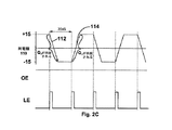
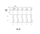
既に指摘され、前述の2003/0137521号において、および同時係属中の特許出願シリアル番号10/814,205号(2004年3月31日出願)および10/879,335号(2004年6月29日出願)において(対応する国際特許出願WO2004/090857号およびPCT/US2004/21000号をそれぞれ参照のこと)詳細に説明されたように、双安定電気光学ディスプレイは、第1近似としてインパルストランスデューサとして働き、その結果としてピクセルの最終状態は、印加された電界およびこの電界が印加された時間のみならず、電界の印加の前のピクセルの状態にも依存する。さらに、少なくとも多数の粒子ベースの電気光学ディスプレイの場合においては、所与のピクセルを等しい変化を通じてグレーレベル(目視によって、または標準の光学計器によって判定される)に変化するために必要なインパルスは、必ずしも一定ではなく、またそれらは必ずしも交換可能ではないことが、今では判明している。例えば、各ピクセルが便宜的に相互に離れた0(白)、1、2または3(黒)のグレーレベルを表示し得るディスプレイを考える。(レベルの間隔は目視によってまたは計器によって測定されたときに、反射率の百分率の等間隔であり得、しかし他の間隔もまた使用され得る。例えば、間隔はL*に関して等間隔であり得(ここで、L*は通常のCIEの定義を有し、すなわち、
L*=116(R/R0)1/3−16、
ここでRは反射率、R0は標準の反射率の値)、または特定のガンマを提供するように選定され得、2.2のガンマがしばしばモニタに対して適用され、本ディスプレイがモニタの代用として使用される場合には、同じガンマの使用が望ましい。)ピクセルをレベル0から1に変化する(今後便宜上、「0−1遷移」として参照される)ために必要なインパルスは、1−2または2−3遷移に必要とされるそれとしばしば同一ではないことが発見されている。さらに、1−0遷移に必要なインパルスは、必ずしも0−1遷移の反転と同じではない。追加として、一部のシステムは「メモリ」効果を示すことが知られ、すなわち、(例えば)0−1遷移に必要なインパルスは、特定のピクセルが0−0−1、1−0−1または3−0−1遷移の何れを経由するかに依存してある程度変化する(ここでx、y、およびzはすべて時間経過と共に訪れる光学的状態の順番を示す光学的状態0、1、2、および3であり、「x−y−z」の記号は早いものから遅いものへのリストである。)。これらの問題は、必要とされるピクセルを他の状態にドライブする前に、かなりの時間のあいだ全てのピクセルを極限状態の1つにドライブすることによって、低減されまたは克服されるものの、結果として生じる無地の「フラッシュ」はしばしば許容し難いものである。例えば、電子本(electric book)の読者がその本のテキストをスクリーンでスクロールダウンすることを希望するとき、ディスプレイが短い間隔で黒または白の無地にフラッシュする必要がある場合には、読者は注意をそらされ、またはその場所がわからなくなることがあり得る。さらにディスプレイがこのようにフラッシュすることはそのエネルギ消費を増加し、ディスプレイの使用寿命を減少し得る。最終的に、少なくとも一部の場合には、特定の遷移に対して必要とされるインパルスは温度およびディスプレイの合計動作時間によって、および特定のピクセルが所与の遷移の前に特定の光学的状態に保たれた時間によって影響されること、および正確なグレースケールを演出するためにはこれらの要素に対して補償することが望ましいこと、が明らかにされている。したがって、電気光学ディスプレイにおいて良好なイメージの演出を生成するためには、適切に定義されたインパルスを電気光学媒体に印加するための制御方法が必要とされる。
Already pointed out in the aforementioned 2003/0137521 and co-pending patent application serial numbers 10 / 814,205 (filed 31 March 2004) and 10 / 879,335 (29 June 2004) (See corresponding international patent applications WO 2004/090857 and PCT / US2004 / 21000, respectively) in detail), the bistable electro-optic display acts as an impulse transducer as a first approximation, As a result, the final state of the pixel depends not only on the applied electric field and the time that this electric field is applied, but also on the state of the pixel prior to the application of the electric field. Further, in the case of at least a large number of particle-based electro-optic displays, the impulse required to change a given pixel to a gray level (as determined visually or by standard optical instrumentation) through equal changes is It has now been found that they are not necessarily constant and are not necessarily interchangeable. For example, consider a display that can display 0 (white), 1, 2, or 3 (black) gray levels where each pixel is conveniently separated from each other. (Level spacing can be equidistant as a percentage of reflectivity as measured visually or by instrument, but other spacings can also be used. For example, spacing can be equidistant with respect to L * ( Where L * has the usual CIE definition, ie
L * = 116 (R / R 0 ) 1/3 -16,
Where R is the reflectivity, R 0 is the standard reflectivity value), or can be chosen to provide a specific gamma, with a gamma of 2.2 often applied to the monitor and the display is When used as a substitute, it is desirable to use the same gamma. ) The impulse required to change a pixel from level 0 to 1 (referred to as "0-1 transition" for convenience in the future) is often not the same as that required for 1-2 or 2-3 transitions It has been discovered. Furthermore, the impulse required for the 1-0 transition is not necessarily the same as the inversion of the 0-1 transition. In addition, some systems are known to exhibit “memory” effects, ie, the impulses required for (for example) 0-1 transitions are 0-0-1, 1-0-1 or Depending on which of the 3-0-1 transitions are going through, where x, y, and z are all
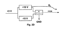
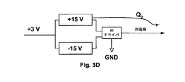
アクティブマトリックス電気光学ディスプレイが書き換えられているとき(すなわち、新しいイメージがディスプレイ上に置かれているとき、またはイメージがリフレッシュされているとき)には、列電極のチャージングおよびディスチャージングは電力消費の重大な原因となり得る。(行電極のチャージングおよびディスチャージングもまた一部の電力を消費するが、しかし、行電極の電力消費ははるかに少ない。なぜならば、任意の所与の行電極はディスプレイ全体を書き込むために使用される時間の間に1度のみチャージおよびディスチャージされるが、列電極はディスプレイの新しい行が書き換えられるたびごとにチャージおよびディスチャージされる必要があり得、一般的にはアクティブマトリックスディスプレイは数百の行を有し得るからである。)このような列電極の電力消費に対する最悪の場合のシナリオは、表示されたイメージの中のストライプまたはチェッカーが反転するときに生じる。この場合、ディスプレイのそれぞれのラインが書き換えられるごとに、それぞれの列のラインはその全電圧範囲にわたってスイッチされ(すなわち、白から黒へまたは黒から白へのピクセルの光学的状態の変化を支援するために)る。この状況において、列電極をチャージおよびディスチャージするために使用される容量性電力は、次によって与えられる。 When the active matrix electro-optic display is being rewritten (ie, when a new image is placed on the display or when the image is refreshed), column electrode charging and discharging is a power consuming. It can be a serious cause. (Row electrode charging and discharging also consume some power, but the power consumption of the row electrode is much less because any given row electrode can be used to write the entire display. The column electrode may need to be charged and discharged every time a new row of the display is rewritten, typically an active matrix display of hundreds (The worst case scenario for such column electrode power consumption occurs when the stripes or checkers in the displayed image are flipped.) In this case, as each line of the display is rewritten, each column line is switched over its full voltage range (i.e. assisting in changing the optical state of the pixel from white to black or from black to white). For) In this situation, the capacitive power used to charge and discharge the column electrodes is given by:
P=1/2fCV2 (A)
ここでPはディスプレイを走査する間に消費される電力を、Cはスイッチされる全ての列電極の結合された電気容量を、Vは列ドライバの全「スイング電圧」(すなわち、全電圧動作範囲)を、およびfは列電極において見られる波形の有効な周波数である。
P = 1/2 fCV 2 (A)
Where P is the power consumed while scanning the display, C is the combined capacitance of all column electrodes that are switched, and V is the total “swing voltage” of the column driver (ie, the full voltage operating range). ), And f are the effective frequencies of the waveform seen at the column electrodes.
一部の電気光学ディスプレイのような、比較的高い電圧を使用するディスプレイにおいては、ディスプレイによって消費される電力の大部分はこの原因から起こり得る。一局面において、本発明は列電極のスイッチングによる電力消費を低減する、アクティブマトリックス電気光学ディスプレイをドライブするための方法を提供することを追求する。本発明はまた、この方法を実行するために使用される修正されたドライバを提供する。これらのドライバは平均値およびピーク値の両方の消費電力を減少するように設計され得る。 In displays that use relatively high voltages, such as some electro-optic displays, most of the power consumed by the display can come from this cause. In one aspect, the present invention seeks to provide a method for driving an active matrix electro-optic display that reduces power consumption due to column electrode switching. The present invention also provides a modified driver that is used to perform this method. These drivers can be designed to reduce both average and peak power consumption.
既に述べたとおり、本発明の第2の局面は大面積の電気光学ディスプレイ、およびこの種の大面積ディスプレイと共に使用されるドライバに関する。詳細には、発明のこの局面は、このような大面積電気光学ディスプレイをドライブするための統合された制御器ロジックを含むディスプレイドライバに関する。 As already mentioned, the second aspect of the present invention relates to a large area electro-optic display and a driver for use with such a large area display. In particular, this aspect of the invention relates to display drivers that include integrated controller logic for driving such large area electro-optic displays.
伝統的に、エレクトロニック(電気光学を含む)ディスプレイは剛な支持構造に取り付けられた構成部品を含む剛なデバイスである。大面積のディスプレイを製造するためには、サブシステムを剛なフレームに取り付けることによって、複数の剛なディスプレイサブシステムが結合されてきた。このような大面積ディスプレイは重く高価であり得、より大きな寸法への拡張性においては大きな制約があり得る。本発明は、プリンティングおよび積層(laminating)のステップをを含む低コストプロセスを使用して、比較的安価な材料およびサブ構成部品から製造され得る柔軟性のある大面積電気光学ディスプレイを提供することを追求する。 Traditionally, electronic (including electro-optic) displays are rigid devices that include components attached to a rigid support structure. To manufacture large area displays, multiple rigid display subsystems have been combined by attaching the subsystem to a rigid frame. Such large area displays can be heavy and expensive, and can be severely limited in scalability to larger dimensions. The present invention provides a flexible large area electro-optic display that can be manufactured from relatively inexpensive materials and sub-components using a low-cost process that includes printing and laminating steps. pursue.
かくして、電気光学ディスプレイを含む大面積標識は、同様の伝統的ディスプレイに対して多くの利点を有するように作られ得る。これらの利点は、軽量、低い消費電力、様々な照明条件下での視認性、拡張性、および改善された大面積製造可能性を含み得る。このような標識は効果的にメンテナンスフリーおよびウエザープルーフであり、屋内および屋外の両方で使用され得る。かくして、電気光学ディスプレイを使用する大面積標識は、広範囲のコマーシャルおよび非コマーシャル用途において特に望まれる。 Thus, large area signs including electro-optic displays can be made to have many advantages over similar traditional displays. These benefits may include light weight, low power consumption, visibility under various lighting conditions, scalability, and improved large area manufacturability. Such signs are effectively maintenance free and weather proof and can be used both indoors and outdoors. Thus, large area signs using electro-optic displays are particularly desirable in a wide range of commercial and non-commercial applications.
しかしながら、このような大面積標識の構造における1つのチャレンジはドライブエレクトロニクスの設計である。上で説明したとおり、電気光学媒体のドライブ要求は、一般的に、液晶ディスプレイをドライブするために設計された既知のドライバを、用途に応じた修正なしには双安定電気光学ディスプレイをドライブするための使用に適さなくする。 However, one challenge in the construction of such large area signs is the design of drive electronics. As explained above, the drive requirements for electro-optic media generally drive known drivers designed to drive liquid crystal displays and to drive bistable electro-optic displays without modification depending on the application. Make it unsuitable for use.
電気光学ディスプレイをドライブするために特別に設計された回路ドライバが、前述の2003/0137521号、WO2004/090857号およびPCT/US2004/21000号に記載されている。これらのドライバは、しかしながら、アクティブマトリックスディスプレイのデータラインをドライブするために最適化されており、それ故に外部ロジックを含まず、ドライバからドライバへとカスケードしないシフトレジスタを備える。これは、このドライバを使用する大面積のまたは長い標識において、制御器はディスプレイが更新される前に、所与の行のそれぞれのピクセルに対して、ディスプレイピクセルごとに2ビットを順次ロードしなければならないことを意味する。このようなデータのローディングは非常に長い時間を要し得る。また、データは一般的に比較的高い周波数で伝達されるために、データパスは不必要に脆弱となり得、データの劣化(corruption)を引き起こす可能性がある。 Circuit drivers specially designed for driving electro-optic displays are described in the aforementioned 2003/0137521, WO 2004/090857 and PCT / US 2004/21000. These drivers, however, are optimized to drive the data lines of the active matrix display and thus include shift registers that do not include external logic and do not cascade from driver to driver. This means that in large area or long signs using this driver, the controller must load 2 bits per display pixel sequentially for each pixel in a given row before the display is updated. It means you have to. Such data loading can take a very long time. Also, since data is generally transmitted at a relatively high frequency, the data path can be unnecessarily fragile, which can cause data corruption.
本発明は電気光学ディスプレイを含む大面積標識のための公知のドライバの短所を解消するドライバを提供することを追求する。詳細には、本発明は文字データを多数のディスプレイドライバに比較的低い帯域幅で送ることを許容するドライバを提供することを追求し、それによって電力消費を低減しデータの劣化の可能性を減少する。本発明はまた、低電圧のデータインターフェイスの使用により、ディスプレイから発する電磁的干渉の量を減少し、既存の文字ディスプレイモジュールと互換性を有するドライバを提供することを追求し、同じ標識の中に異種の混合したディスプレイドライバを含むディスプレイを可能とする。最終的に、本発明は制御器の機能と電気光学媒体との間の改善された統合を提供し、それによって各ディスプレイモジュールは事実上自己専用の制御器を所有することを追求し、かくして、標識の残りの構成部品の動作には影響を与えることなく、個々のモジュールが、潜在的に劇的に異なる特性を有するより新しいモデルによって置き換えられることを可能とする。 The present invention seeks to provide a driver that overcomes the disadvantages of known drivers for large area signs including electro-optic displays. Specifically, the present invention seeks to provide a driver that allows character data to be sent to a large number of display drivers with a relatively low bandwidth, thereby reducing power consumption and reducing the possibility of data degradation. To do. The present invention also seeks to provide a driver that reduces the amount of electromagnetic interference emanating from the display through the use of a low voltage data interface and is compatible with existing character display modules, within the same sign. Enables displays that include disparate mixed display drivers. Finally, the present invention provides improved integration between the controller functions and the electro-optic medium, whereby each display module seeks to have a virtually self-dedicated controller and thus Without affecting the operation of the remaining components of the sign, individual modules can be replaced by newer models with potentially dramatically different characteristics.
一局面においては、この発明は電気光学媒体を有する電気光学ディスプレイ、電気光学媒体に電界を印加することのできるピクセル電極、およびピクセル電極と関連する列電極をドライブする方法を提供し、その方法は列電極上の電圧を第1の値から第1の値とは異なる第2の値に変化すること、それによってピクセル電極が電気光学媒体の光学的状態に変化を起こさせるようにすることを含み、列電極上の電圧は最初は、チャージが列電極へまたはから流れることを許容する充分な時間の間、第1の値から第1および第2の値の間の第3の値に変化し、その後列電極上の電圧は第3の電圧から第2の電圧に変化する。 In one aspect, the present invention provides an electro-optic display having an electro-optic medium, a pixel electrode capable of applying an electric field to the electro-optic medium, and a method of driving a column electrode associated with the pixel electrode, the method comprising: Changing the voltage on the column electrode from a first value to a second value different from the first value, thereby causing the pixel electrode to change the optical state of the electro-optic medium. The voltage on the column electrode initially changes from a first value to a third value between the first and second values for a time sufficient to allow charge to flow to or from the column electrode. Thereafter, the voltage on the column electrode changes from the third voltage to the second voltage.
本発明のこの局面は、今後便宜的に本発明の「2ステップ電圧変化法」(「TSVCM」)として参照される。しかしながら、この方法は2つのステップのみを使用することに限定されず、第1と第2の電圧の間の1つより多いの中間電圧を使用する、2つより多いステップを用いても実行され得ることが、理解される。 This aspect of the present invention will be referred to hereinafter as the “two-step voltage change method” (“TSVCM”) of the present invention for convenience. However, this method is not limited to using only two steps, and is also performed with more than two steps using more than one intermediate voltage between the first and second voltages. It is understood that you get.
発明の2ステップ電圧変化法において、第1および第2の電圧は反対の極性であり得、第3の電圧はグラウンド電圧であり得る。第3の電圧は第1および第2の電圧の算術平均値と実質的に等しくあり得る。アクティブマトリックスディスプレイにおいて一般的にそうであるように、ディスプレイが電気光学媒体のピクセル電極から反対の側に配置されたフロント電極を備えるときには、フロント電極は実質的に一定の電圧に保持され、第3の電圧はフロント電極上の電圧と等しいか、または実質的に等しくあり得る。また、一般的な場合であるように、ディスプレイが、列電極と接続され第1、第2および第3の電圧をそこに印加するために配置された列ドライバ、および列ドライバに少なくとも2つの電圧を供給するために配置された電圧供給手段を備えるときには、共通電極上の電圧が第3の値に設定されるとき、列電極へまたはそこから流れるチャージが電圧供給手段を通過しないように、TSVCMは有効に働き得る。 In the two-step voltage change method of the invention, the first and second voltages can be of opposite polarity and the third voltage can be a ground voltage. The third voltage may be substantially equal to the arithmetic average value of the first and second voltages. As is generally the case with active matrix displays, when the display comprises a front electrode disposed on the opposite side from the pixel electrode of the electro-optic medium, the front electrode is held at a substantially constant voltage, and the third May be equal to or substantially equal to the voltage on the front electrode. Also, as is the general case, a display is connected to the column electrode and arranged to apply first, second and third voltages thereto, and at least two voltages on the column driver. When the voltage supply means arranged for supplying the voltage is provided, when the voltage on the common electrode is set to the third value, the TSVCM is prevented so that the charge flowing to or from the column electrode does not pass through the voltage supply means. Can work effectively.
電気光学ディスプレイ技術の当業者にとって周知のとおり、このようなディスプレイは通常列電極と接続される列ドライバを使用し、この列電極はオンおよびオフ状態を有する「出力イネーブル」(「OE」)入力を有し、その結果として、OE入力がオン状態であるときには、列ドライバは少なくとも3つの異なる電圧を列電極に印加し得、しかしOE入力がオフ状態であるときには、列ドライバは1つのみの電圧(通常は共通フロント電極の電圧)を列電極に印加し得る。本発明のTSVCMがこのようなディスプレイに使用されるとき、最初にOE入力をオフ状態に設定することで、列ドライバをして列電極に第3の電圧を印加させ、次いでOE入力をオン状態に設定することで、列ドライバをして列電極に第2の電圧を印加させることによって、その方法は有効に働き得る。また、以下により詳細に説明するように、TSVCMは列電極の初期の状態をその所望の最終の状態と比較するステップを含み、列電極の2つの状態が異なるときにのみOE入力をオフ状態に設定することが、実際には望ましい。より詳細には、電気光学ディスプレイが複数の列電極および複数のピクセル電極を備え、各ピクセル電極は1つの列電極と接続される、従来の種類である場合には、TSVCMにおいては、ディスプレイ上のイメージが書き換えられつつあるとき、書き換えのプロセスの1ステップの間のそれぞれの列電極上の初期電圧が、書き換えのプロセスの次のステップの間の列電極上の最終電圧と比較され得、初期および最終電圧が異なる列電極のみに対して第3の電圧が印加される。 As is well known to those skilled in the electro-optic display art, such a display typically uses a column driver connected to a column electrode, which has an “output enable” (“OE”) input having an on and off state. As a result, when the OE input is on, the column driver can apply at least three different voltages to the column electrode, but when the OE input is off, there is only one column driver. A voltage (usually the voltage of the common front electrode) can be applied to the column electrodes. When the TSVCM of the present invention is used in such a display, the column driver is first applied to the column electrode by setting the OE input to the off state, and then the OE input is turned on. By setting to, the method can work effectively by having the column driver apply a second voltage to the column electrodes. Also, as described in more detail below, TSVCM includes a step of comparing the initial state of the column electrode with its desired final state, and only turns off the OE input when the two states of the column electrode are different. Setting is actually desirable. More particularly, if the electro-optic display is a conventional type, comprising a plurality of column electrodes and a plurality of pixel electrodes, each pixel electrode being connected to one column electrode, in TSVCM, on the display When the image is being rewritten, the initial voltage on each column electrode during one step of the rewriting process can be compared with the final voltage on the column electrode during the next step of the rewriting process, The third voltage is applied only to the column electrodes having different final voltages.
TSVCMは、例えば前述のE InkおよびMITの特許および特許出願のいくつかにおいて記載されているような、各ピクセル電極が分離した導電性のトレース(「列電極」)を備え、それによってピクセル電極上の電圧が制御され得る、いわゆる「ダイレクトドライブ」ディスプレイを含む任意の種類の電気光学ディスプレイに適用され得る。TSVCMはまた、パッシブマトリックスアドレスドディスプレイにも使用され得る。しかしながら、TSVCMは特に、電気光学媒体の1側面上にピクセル電極の2次元アレイを有し、電気光学媒体の反対の側面上に共通電極を有し、複数の列電極はピクセル電極の2次元アレイの列と接続され、複数の行電極はピクセル電極の2次元アレイの行と接続され、その結果各ピクセル電極は1つの特定の列電極と1つの特定の行電極との交差によって一義的に定義される、アクティブマトリックスディスプレイにおいて使用されることが意図される。 The TSVCM comprises a conductive trace ("column electrode") with each pixel electrode separated, as described, for example, in some of the aforementioned E Ink and MIT patents and patent applications, thereby allowing the pixel electrode to Can be applied to any type of electro-optic display, including so-called “direct drive” displays, in which the voltage can be controlled. TSVCM can also be used for passive matrix addressed displays. However, TSVCM specifically has a two-dimensional array of pixel electrodes on one side of the electro-optic medium, a common electrode on the opposite side of the electro-optic medium, and the plurality of column electrodes are two-dimensional arrays of pixel electrodes. A plurality of row electrodes connected to a row of a two-dimensional array of pixel electrodes, so that each pixel electrode is uniquely defined by the intersection of one specific column electrode and one specific row electrode Intended to be used in an active matrix display.
TSVCMは上述された任意のものを含む、任意の種類の電気光学媒体に使用され得る。かくして、例えば電気光学媒体は、回転バイクロマルメンバーまたはエレクトロクロミック媒体、または懸濁流体および懸濁流体の中に保持され、懸濁流体への電界の印加によって運動可能な複数の電気的にチャージされた粒子を備える、粒子ベースの電気泳動媒体であり得る。懸濁流体は液体または気体であり得る。電気泳動媒体は、懸濁流体および電気的にチャージされた粒子を複数の離散したドロップレット(恐らく、懸濁流体が気体のときには「ボイド」として参照される方がよい)に分離する連続した相を有する、カプセル化された媒体であり得る。 TSVCM can be used for any type of electro-optic medium, including any of those described above. Thus, for example, an electro-optic medium is held in a rotating bichromal member or electrochromic medium, or suspension fluid and suspension fluid, and is electrically charged by a plurality of electrically charged media that can be moved by application of an electric field to the suspension fluid. It can be a particle-based electrophoretic medium comprising the particles. The suspending fluid can be a liquid or a gas. An electrophoretic medium is a continuous phase that separates a suspended fluid and electrically charged particles into a plurality of discrete droplets (perhaps better referred to as “voids” when the suspended fluid is a gas). Can be an encapsulated medium.
本発明はまた、発明の2ステップ電圧制御法に使用されるための装置を提供する。かくして、この発明は電気光学媒体、電界を印加することが可能なピクセル電極、およびピクセル電極と関連する列電極を有する電気光学ディスプレイをドライブするための装置を提供する。該装置は、
列電極に少なくとも第1、第2および第3の電圧を印加でき、第1および第2の電圧は相互に異なり、第3の電圧は第1および第2の電圧の間にある、列ドライバと、
いつ、列が列電極に印加される電圧を第1の電圧から第2の電圧に変化する必要があるかを決定し、このような変化の必要性が検出されるとき、列電極にまたはからチャージが流れるための十分な時間の間、列ドライバをして列電極に最初に第3の電圧を印加させ、その後、列ドライバをして列電極に第2の電圧を印加させるように配置される、ロジック手段と、を備える。
The present invention also provides an apparatus for use in the inventive two-step voltage control method. Thus, the present invention provides an apparatus for driving an electro-optic display having an electro-optic medium, a pixel electrode capable of applying an electric field, and a column electrode associated with the pixel electrode. The device
A column driver capable of applying at least first, second and third voltages to the column electrodes, wherein the first and second voltages are different from each other and the third voltage is between the first and second voltages; ,
Determine when the column needs to change the voltage applied to the column electrode from the first voltage to the second voltage, and when the need for such a change is detected, to or from the column electrode Arranged to have the column driver first apply a third voltage to the column electrode for a sufficient time for the charge to flow, and then the column driver to apply the second voltage to the column electrode. Logic means.
別の局面においては、この発明は柔軟性のある基板および柔軟性のある基板に取り付けられる複数の柔軟性のある電気光学ディスプレイユニットを備える、電気光学ディスプレイシステムを提供する。 In another aspect, the present invention provides an electro-optic display system comprising a flexible substrate and a plurality of flexible electro-optic display units attached to the flexible substrate.
本発明のこの局面は、今後便宜的に本発明の「柔軟性のある大面積ディスプレイ」(「FLAD」)として参照され得、それは主として大面積ディスプレイでの使用が意図されるが、それに限定はされない。このような柔軟性のある大面積ディスプレイはさらに、柔軟性のある基板上に複数のディスプレイユニットを固定するための接着剤層を備え得る。一般的に、柔軟性のある基板は光透過性である(例えばディスプレイの色修正または反射防止またはぎらつき防止のための、一部の色の存在は除外されないものの、実質的に透明である)。ディスプレイユニットは上述された様々な種類の電気光学媒体、液晶媒体(ポリマー分散型およびプラスチックベースの液晶媒体を含む)、エレクトロルミネッセンス媒体および有機発光ダイオードを含む、任意の公知のディスプレイ媒体を利用し得る。柔軟性のある基板は任意の公知のフィルタまたは表面処理特性を提供され得、例えば、柔軟性のある基板は紫外線フィルタリング特性、またはぎらつき防止表面処理を有し得る。 This aspect of the present invention may be referred to as the “flexible large area display” (“FLAD”) of the present invention for convenience in the future, which is primarily intended for use in large area displays, but is not limited thereto. Not. Such a flexible large area display may further comprise an adhesive layer for securing a plurality of display units on a flexible substrate. In general, flexible substrates are light transmissive (eg, substantially transparent, although the presence of some colors is not ruled out for color correction or antireflection or glare prevention of the display). . The display unit may utilize any known display medium, including the various types of electro-optic media, liquid crystal media (including polymer dispersed and plastic-based liquid crystal media), electroluminescent media, and organic light emitting diodes described above. . The flexible substrate can be provided with any known filter or surface treatment characteristics, for example, the flexible substrate can have UV filtering properties, or an anti-glare surface treatment.
本発明のFLADにおいては、ディスプレイユニットは一般的には柔軟性のある基板を通して見られる向きに置かれる。FLADは基板に隣接しディスプレイユニットの非活性部分を隠す効果のあるマスクを提供され得る。マスクはディスプレイユニットの色と実質的にマッチする色、またはディスプレイユニットの色を有し得る。接着剤層が存在するときには、一般的にそれは実質的に透明である。接着剤層は、例えば、エチレンビニルアセテート、ポリビニルブチレート、熱硬化性材料、熱可塑性材料、放射線硬化性材料の少なくとも1つを備え得る。接着剤層はシートの形状であり得、または液体を備え得る。 In the FLAD of the present invention, the display unit is generally placed in an orientation as seen through a flexible substrate. The FLAD can be provided with a mask adjacent to the substrate that has the effect of hiding inactive portions of the display unit. The mask may have a color that substantially matches the color of the display unit, or the color of the display unit. When an adhesive layer is present, it is generally substantially transparent. The adhesive layer may comprise at least one of, for example, ethylene vinyl acetate, polyvinyl butyrate, thermosetting material, thermoplastic material, and radiation curable material. The adhesive layer can be in the form of a sheet or can comprise a liquid.
FLADはまた保護膜、および保護膜と柔軟性のある基板との間の第2の接着剤層を備え得る。保護膜は熱成形が可能であり得、および/または実質的に透明なプラスチックシートを備え得る。柔軟性のある基板はポリエステル、アクリル、ポリカーボネート、ポリカーボネート−PVF複合体、および透明なフルオロポリマーの少なくとも1つを備え得る。FLADは接着剤層(存在するときには)の中に埋め込まれた取り付け用のブロックを備え得る。FLADにおいては、ディスプレイユニットはその縁で重なり合うことができる。 The FLAD may also comprise a protective film and a second adhesive layer between the protective film and the flexible substrate. The protective film can be thermoformed and / or can comprise a substantially transparent plastic sheet. The flexible substrate may comprise at least one of polyester, acrylic, polycarbonate, polycarbonate-PVF composite, and transparent fluoropolymer. The FLAD may comprise a mounting block embedded in an adhesive layer (when present). In FLAD, the display units can overlap at their edges.
この発明はまた、電気光学ディスプレイシステムを製造するためのプロセスを提供し、該プロセスは、柔軟性のある基板を提供すること、複数の柔軟性のある電気光学ディスプレイユニットを提供すること、および複数の柔軟性のある電気光学ディスプレイユニットを柔軟性のある基板に貼り付けること、を包含する。 The present invention also provides a process for manufacturing an electro-optic display system, the process providing a flexible substrate, providing a plurality of flexible electro-optic display units, and a plurality of And attaching the flexible electro-optic display unit to a flexible substrate.
この「FLADプロセス」において、ディスプレイユニットは一般的には柔軟性のある基板に積層によって貼り付けれる。このような積層は減圧積層法であり得、加熱を伴って実行され得る。積層はまたロールツーロール積層法であり得る。積層は、エチレンビニルアセテート、ポリアミド、ポリウレタンの少なくとも1つを備える熱い融解した接着剤を使用して実行され得、および/またはシリコン、エポキシ、およびポリウレタンの少なくとも1つを備える液体接着剤を適用することによって達成され得る。 In this “FLAD process”, the display unit is generally attached to a flexible substrate by lamination. Such lamination can be a reduced pressure lamination method and can be performed with heating. Lamination can also be a roll-to-roll lamination process. Lamination can be performed using a hot melt adhesive comprising at least one of ethylene vinyl acetate, polyamide, polyurethane and / or applying a liquid adhesive comprising at least one of silicone, epoxy, and polyurethane. Can be achieved.
別の局面においては、この発明は、それぞれがそれ自身と関連するピクセル電極を有する複数のピクセル、を備えるディスプレイモジュールの上に表示されるイメージを制御するためのディスプレイモジュールドライバデバイスを提供し、該ドライバデバイスは、
初期および最終の表示されるイメージを表すデータを受け取るための入力手段と、
入力手段によって受け取られるデータを初期および最終のイメージのピクセルワイズ(pixel−wise)表現に変換(tranalate)するための変換手段と、
初期および最終のイメージのピクセルワイズ表現を蓄えるための貯蔵手段と、
ディスプレイのピクセル電極に印加される電圧を制御するために配置される複数の出力手段と、
貯蔵手段からデータを受け取り、このデータから複数の出力手段において要求される出力を生成するために配置されるロジック手段と、を備える。
In another aspect, the present invention provides a display module driver device for controlling an image displayed on a display module comprising a plurality of pixels, each having a pixel electrode associated with it, The driver device is
Input means for receiving data representing the initial and final displayed images;
Transformation means for translating data received by the input means into pixel-wise representations of the initial and final images;
A storage means for storing pixel-wise representations of the initial and final images;
A plurality of output means arranged to control the voltage applied to the pixel electrodes of the display;
Logic means arranged to receive data from the storage means and generate the required output at the plurality of output means from this data.
本発明のこのディスプレイモジュールドライバデバイス(「DMDD」)において、ロジック手段は、環境パラメータ、ディスプレイモジュールの動作寿命を表すパラメータ、およびディスプレイモジュールの電気光学特性を表すパラメータの少なくとも1つに依存して、出力手段における出力を変更するように配置され得る。 In this display module driver device (“DMDD”) of the present invention, the logic means depends on at least one of environmental parameters, parameters representing the operating lifetime of the display module, and parameters representing the electro-optical characteristics of the display module, It can be arranged to change the output at the output means.
DMDDは主として、上述された任意の種類の電気光学媒体を含む電気光学ディスプレイに使用されることが意図される。DMDDは上述されたダイレクトドライブ型のディスプレイにおいて特に有用であり得、それは、それぞれが分離した電極を備える連続したピクセルに分割され、ディスプレイはそれぞれの分離した電極に印加される電圧を独立に制御するために配置されるスイッチング手段を、さらに備える。DMDDはまた、各ピクセルへのドライバ接続を提供するための全コストが電気光学媒体のコストなどのほかのコストと比較して相対的に低い、大面積のダイレクトドライブされるマトリックスディスプレイに対しても有用であり得る。 DMDD is primarily intended for use in electro-optic displays that include any of the types of electro-optic media described above. DMDD can be particularly useful in the direct drive type display described above, which is divided into successive pixels, each with a separate electrode, and the display independently controls the voltage applied to each separate electrode. Switching means arranged for the purpose is further provided. DMDD is also for large area direct-driven matrix displays where the total cost to provide a driver connection to each pixel is relatively low compared to other costs such as the cost of electro-optic media. Can be useful.
この発明はまた、複数のディスプレイモジュールおよびディスプレイアセンブリ入力手段を備えるディスプレイアセンブリ(本発明の「DMDDアセンブリ」)を提供し、各ディスプレイモジュールはそれ自身と関連しその関連するディスプレイモジュール上に表示されるイメージを制御するために配置される本発明のディスプレイモジュールドライバデバイスを有し、ディスプレイアセンブリ入力手段はディスプレイアセンブリ上に表示されるイメージを表すイメージデータを受け取り、イメージデータの少なくとも部分を各ディスプレイモジュールドライバデバイスに提供するために配置される。 The present invention also provides a display assembly comprising a plurality of display modules and display assembly input means (the “DMDD assembly” of the present invention), each display module associated with itself and displayed on its associated display module. A display module driver device of the present invention arranged to control an image, wherein the display assembly input means receives image data representing an image displayed on the display assembly, and at least a portion of the image data is received for each display module driver. Arranged to provide to the device.
このようなDMDDアセンブリにおいて、様々なDMDDの間でイメージデータを分配することは任意の公知の方法で達成され得、このようなデータ分配の好ましい方法が以下に詳細に記載される。一般的にはDMDDは「デージーチェーン」を成し、各DMDDはチェーンの次のDMDDの入力手段と接続されるデータ出力手段(ピクセル上の電圧を制御する出力手段とは分離される)を有する。 In such a DMDD assembly, distributing image data among various DMDDs can be accomplished in any known manner, and preferred methods of such data distribution are described in detail below. In general, DMDD forms a “daisy chain”, and each DMDD has data output means (separated from output means for controlling the voltage on the pixel) connected to the input means of the next DMDD in the chain. .
本発明のDMDDは、前述の2003/0137521号、WO2004/090857号およびPCT/US2004/21000号に記載された任意のドライビング方法を、温度、相対湿度、電気光学媒体の動作寿命時間などに対する修正のような、このようなドライビング方法の様々な任意の局面を含んで、実行するために配置され得る。従ってDMDDは、このようなドライビング方法に対して必要とされる追加の電子的デバイスまたはセンサ、例えば温度または湿度センサ、または関連する電気光学ディスプレイモジュールの動作時間を測定するためのタイマーを組み込み得る。
例えば、本発明は以下の項目を提供する。
(項目1)
電気光学媒体と、該電気光学媒体に電界を印加することができるピクセル電極と、該ピクセル電極と関連する列電極とを有する電気光学ディスプレイをドライブするための方法であって、
該列電極上の電圧を第1の値から該第1の値とは異なる第2の値に変えることと、それによって該ピクセル電極をして該電気光学媒体の光学的状態に変化を生じさせることと、
を包含し、該方法は、
該列電極上の該電圧は、最初に、該列電極へまたはそこからチャージが流れることを許容する充分な時間の間、該第1の値から該第1および第2の値の間の第3の値に変更され、その後、該列電極上の該電圧は該第3の値から該第2の値に変更されることを特徴とする、方法。
(項目2)
前記第1および第2の電圧は逆の極性を有し、該第3の電圧はグラウンド電圧である、項目1に記載の方法。
(項目3)
前記第3の電圧は前記第1および第2の電圧の算術平均値と実質的に等しい、項目1に記載の方法。
(項目4)
前記ディスプレイは、前記電気光学媒体の、前記ピクセル電極とは反対の側に配置されるフロント電極をさらに備え、該フロント電極は実質的に一定の電圧に保持され、前記第3の電圧は該フロント電極の該電圧と実質的に等しい、項目1に記載の方法。
(項目5)
前記ディスプレイは、前記列電極と接続されそこに前記第1、第2および第3の電圧を印加するように配置される列ドライバと、該列ドライバに少なくとも2つの電圧を供給するように配置される電圧供給手段とをさらに備え、共通電極上の前記電圧が前記第3の値にセットされるとき、前記列電極へまたはそこから流れる前記チャージが該電圧供給手段を通過しない、項目1に記載の方法。
(項目6)
前記ディスプレイは、前記列電極と接続される列ドライバをさらに備え、前記列電極はオンおよびオフ状態を有するOE入力を有し、該OE入力がそのオン状態にあるときには該列ドライバは前記第1、第2および第3の電圧を前記列電極に印加でき、しかし該OE入力がそのオフ状態にあるときには該列ドライバは前記第3の電圧のみを前記列電極に印加でき、
前記方法は、最初に該OE入力を該オフ状態にセットすることによって、該列ドライバをして前記列電極に前記第3の電圧を印加させ、その後該OE入力をそのオン状態にセットすることによって、該列ドライバをして前記列電極に前記第2の電圧を印加させることによって達成される、項目1に記載の方法。
(項目7)
前記列電極の初期状態を前記列電極の所望の最終状態と比較することと、前記列電極の該2つの状態が異なる場合にのみ、前記OE入力をそのオフ状態にセットすることとをさらに包含する、項目6に記載の方法。
(項目8)
前記電気光学ディスプレイは複数の列電極および複数のピクセル電極を備え、それぞれのピクセル電極は1つの列電極と接続され、
前記ディスプレイ上のイメージが書き換えられつつあるときに、該書き換えプロセスの1ステップの間のそれぞれの列電極上の初期電圧が、該書き換えプロセスの次のステップの間の該列電極上の最終電圧と比較され、該初期圧とおよび最終電圧とが異なる該列電極に対してのみ前記第3の電圧が印加される、項目1に記載の方法。
(項目9)
前記電気光学ディスプレイは、前記電気光学媒体の一方の側のピクセル電極の二次元アレイ、および前記電気光学媒体の反対の側の共通電極と、ピクセル電極の該二次元アレイの列と接続された複数の列電極と、ピクセル電極の該二次元アレイの行と接続された複数の行電極とを有するアクティブマトリックスディスプレイであって、それぞれのピクセル電極は1つの特定の列電極および1つの特定の行電極の交差によって一義的に定義される、項目1に記載の方法。
(項目10)
前記電気光学媒体は、回転バイクロマルメンバーまたはエレクトロクロミック媒体である、項目1に記載の方法。
(項目11)
前記電気光学媒体は、懸濁流体と、該懸濁流体の中に保持され該懸濁流体への電界の印加によってそこで運動が可能な複数の電気的にチャージされた粒子とを備える、粒子ベースの電気泳動媒体である、項目1に記載の方法。
(項目12)
前記電気泳動媒体は、前記懸濁流体および前記電気的にチャージされた粒子を複数の離散したドロップレットに分離する連続した相を有する、カプセル化された媒体である、項目11に記載の方法。
(項目13)
電気光学媒体と、電界を印加することができるピクセル電極と、該ピクセル電極と関連する列電極と、を有する電気光学ディスプレイをドライブするための装置であって、
少なくとも第1、第2および第3の電圧を該列電極に印加することができ、該第1および第2の電圧は相互に異なり、該第3の電圧は該第1および第2の電圧の間にある、列ドライバを備え、該装置は、
いつ、列が該列電極に印加される該電圧を該第1の電圧から該第2の電圧に変更することを必要とするかを決定し、このような変更の必要性が検出されるとき、該列ドライバをして最初に、該列電極へまたはそこからチャージが流れることを許容する充分な時間の間、該列電極に該第3の電圧を印加させ、その後、該列ドライバをして該列電極上に該第2の電圧を印加させるように配置される、ロジック手段を特徴とする、装置。
(項目14)
前記第1および第2の電圧は逆の極性を有し、該第3の電圧はグラウンド電圧である、項目13に記載の装置。
(項目15)
前記第3の電圧は前記第1および第2の電圧の算術平均値と実質的に等しい、項目13に記載の装置。
(項目16)
前記列ドライバに少なくとも2つの電圧を供給するように配置される電圧供給手段をさらに備え、
前記ロジック手段は、共通電極上の前記電圧が前記第3の値にセットされるとき、前記列をして前記列電極へまたはそこから流れる前記チャージを迂回させ、その結果、このチャージが該電圧供給手段を通過しないように配置される、項目13に記載の装置。
(項目17)
前記列電極はオンおよびオフ状態を有するOE入力を有し、該OE入力がそのオン状態にあるときには該列ドライバは前記第1、第2および第3の電圧を前記列電極に印加でき、しかし該OE入力がそのオフ状態にあるときには該列ドライバは前記第3の電圧のみを前記列電極に印加でき、
前記ロジック手段は、最初に該OE入力を該オフ状態にセットすることによって、該列ドライバをして前記列電極に前記第3の電圧を印加させ、その後該OE入力をそのオン状態にセットすることによって、該列ドライバをして前記列電極に前記第2の電圧を印加させるように配置される、
項目13に記載の装置。
(項目18)
前記ロジック手段は、前記列電極の初期状態を前記列電極の所望の最終状態と比較し、前記列電極の該2つの状態が異なる場合にのみ、前記OE入力をそのオフ状態にセットするように配置される、項目17に記載の装置。
(項目19)
電気光学媒体の層と、該電気光学媒体と隣接して配置されるピクセル電極と、該電気光学媒体と隣接してその反対の側に配置されるフロント電極と、該ピクセル電極と関連する列電極と、を備える電気光学ディスプレイであって、
該ディスプレイは項目13に記載の装置を備えることを特徴とし、該装置の列ドライバは該列電極およびフロント電極に印加される前記電圧を制御するように配置される、電気光学ディスプレイ。
(項目20)
前記電気光学媒体は、回転バイクロマルメンバーまたはエレクトロクロミック媒体である、項目19に記載の電気光学ディスプレイ。
(項目21)
前記電気光学媒体は、懸濁流体と、該懸濁流体の中に保持され該懸濁流体への電界の印加によってそこで運動が可能な複数の電気的にチャージされた粒子とを備える、粒子ベースの電気泳動媒体である、項目19に記載の電気光学ディスプレイ。
(項目22)
前記電気泳動媒体は、前記懸濁流体および前記電気的にチャージされた粒子を複数の離散したドロップレットに分離する連続した相を有する、カプセル化された媒体である、項目21に記載の電気光学ディスプレイ。
(項目23)
柔軟性のある基板と、該柔軟性のある基板に取り付けられる複数の柔軟性のある電気光学ディスプレイユニットとを特徴とする、電気光学ディスプレイシステム。
(項目24)
柔軟性のある基板を提供することと、複数の柔軟性のある電気光学ディスプレイユニットを提供することと、該複数の柔軟性のある電気光学ディスプレイユニットを該柔軟性のある基板に貼り付けることとを特徴とする、電気光学ディスプレイシステムを製造するためのプロセス。
(項目25)
それに関連するピクセル電極をそれぞれ有する複数のピクセルを備えるディスプレイモジュールの上に表示されるイメージを制御するためのディスプレイモジュールドライバデバイスであって、
表示される初期および最後のイメージを表すデータを受信するための入力手段と、
該入力手段によって受信された該データを、該初期および最後のイメージのピクセルワイズ表現に変換するための変換手段と、
該初期および最後のイメージの該ピクセルワイズ表現を蓄えるための貯蔵手段と、
該ディスプレイの該ピクセル電極に印加される電圧を制御するように配置される複数の出力手段と、
該貯蔵手段からデータを受信し、このデータから該複数の出力手段上に要求される出力を生成するように配置されるロジック手段と、
を特徴とする、ディスプレイモジュールドライバデバイス。
(項目26)
前記ロジック手段は、環境パラメータ、前記ディスプレイモジュールの動作寿命を表すパラメータおよび前記ディスプレイモジュールの電気光学特性を表すパラメータのうちの少なくとも1つに依存して、前記出力手段における出力を変更するように配置される、項目25に記載のディスプレイモジュールドライバデバイス。
(項目27)
ディスプレイモジュールと関連しその関連するディスプレイモジュール上に表示されるイメージを制御するように配置される、項目25に記載のディスプレイモジュールドライバデバイスをそれぞれ有する、複数のディスプレイモジュールと、
ディスプレイアセンブり上に表示されるイメージを表すイメージデータを受信し、それぞれのディスプレイモジュールドライバデバイスに該イメージデータの少なくとも部分を提供するように配置される、ディスプレイアセンブリ入力手段と、
を特徴とする、ディスプレイアセンブリ。
The DMDD of the present invention can be applied to any of the driving methods described in the aforementioned 2003/0137521, WO 2004/090857, and PCT / US2004 / 21000 to correct the temperature, relative humidity, operating lifetime of the electro-optic medium, and the like. Can be arranged to perform, including various optional aspects of such driving methods. Thus, the DMDD may incorporate a timer for measuring the operating time of additional electronic devices or sensors required for such driving methods, such as temperature or humidity sensors, or related electro-optic display modules.
For example, the present invention provides the following items.
(Item 1)
A method for driving an electro-optic display having an electro-optic medium, a pixel electrode capable of applying an electric field to the electro-optic medium, and a column electrode associated with the pixel electrode,
Changing the voltage on the column electrode from a first value to a second value different from the first value, thereby causing the pixel electrode to change the optical state of the electro-optic medium And
Wherein the method comprises:
The voltage on the column electrode is initially set between the first value and the first and second values for a sufficient time to allow charge to flow to or from the column electrode. The method is characterized in that it is changed to a value of 3 and then the voltage on the column electrode is changed from the third value to the second value.
(Item 2)
The method of item 1, wherein the first and second voltages have opposite polarities and the third voltage is a ground voltage.
(Item 3)
The method of claim 1, wherein the third voltage is substantially equal to an arithmetic average value of the first and second voltages.
(Item 4)
The display further includes a front electrode disposed on a side of the electro-optic medium opposite to the pixel electrode, the front electrode being held at a substantially constant voltage, and the third voltage being the front voltage.
(Item 5)
The display is arranged to connect to the column electrode and be arranged to apply the first, second and third voltages thereto, and to supply at least two voltages to the column driver. The voltage supply means is further provided, and when the voltage on the common electrode is set to the third value, the charge flowing to or from the column electrode does not pass through the voltage supply means. the method of.
(Item 6)
The display further includes a column driver connected to the column electrode, the column electrode having an OE input having an on state and an off state, and when the OE input is in the on state, the column driver is the first driver. , Second and third voltages can be applied to the column electrode, but the column driver can apply only the third voltage to the column electrode when the OE input is in its off state;
The method first causes the column driver to apply the third voltage to the column electrode by setting the OE input to the off state, and then sets the OE input to its on state. The method of item 1, wherein the method is accomplished by causing the column driver to apply the second voltage to the column electrode.
(Item 7)
Comparing the initial state of the column electrode with the desired final state of the column electrode and setting the OE input to its off state only if the two states of the column electrode are different. The method according to item 6, wherein:
(Item 8)
The electro-optic display includes a plurality of column electrodes and a plurality of pixel electrodes, and each pixel electrode is connected to one column electrode;
When the image on the display is being rewritten, the initial voltage on each column electrode during one step of the rewriting process is the final voltage on the column electrode during the next step of the rewriting process. The method according to item 1, wherein the third voltage is applied only to the column electrodes that are compared and have different initial pressure and final voltage.
(Item 9)
The electro-optic display includes a two-dimensional array of pixel electrodes on one side of the electro-optic medium, a plurality of common electrodes on opposite sides of the electro-optic medium, and a plurality of columns connected to the columns of the two-dimensional array of pixel electrodes. Active column display and a plurality of row electrodes connected to the rows of the two-dimensional array of pixel electrodes, each pixel electrode having one specific column electrode and one specific
(Item 10)
(Item 11)
The electro-optic medium comprises a suspending fluid and a plurality of electrically charged particles retained in the suspending fluid and capable of moving there by application of an electric field to the suspending
(Item 12)
12. The method of item 11, wherein the electrophoretic medium is an encapsulated medium having a continuous phase that separates the suspending fluid and the electrically charged particles into a plurality of discrete droplets.
(Item 13)
An apparatus for driving an electro-optic display having an electro-optic medium, a pixel electrode to which an electric field can be applied, and a column electrode associated with the pixel electrode,
At least a first, second and third voltage can be applied to the column electrode, the first and second voltages being different from each other, and the third voltage being equal to the first and second voltages. A column driver in between, the device comprising:
Determining when a column needs to change the voltage applied to the column electrode from the first voltage to the second voltage, and when the need for such a change is detected The column driver is first applied with the third voltage to the column electrode for a time sufficient to allow charge to flow to or from the column electrode, and then the column driver is turned on. And a logic means arranged to apply the second voltage on the column electrode.
(Item 14)
14. The apparatus of item 13, wherein the first and second voltages have opposite polarities and the third voltage is a ground voltage.
(Item 15)
14. The apparatus of item 13, wherein the third voltage is substantially equal to an arithmetic average value of the first and second voltages.
(Item 16)
Voltage supply means arranged to supply at least two voltages to the column driver;
The logic means causes the column to bypass the charge flowing to or from the column electrode when the voltage on the common electrode is set to the third value, so that the charge is the voltage 14. Apparatus according to item 13, arranged so as not to pass through the supply means.
(Item 17)
The column electrode has an OE input having an on and off state, and the column driver can apply the first, second and third voltages to the column electrode when the OE input is in the on state; When the OE input is in its off state, the column driver can apply only the third voltage to the column electrode;
The logic means first sets the OE input to the off state, causing the column driver to apply the third voltage to the column electrode, and then sets the OE input to its on state. And arranged to cause the column driver to apply the second voltage to the column electrode,
Item 14. The device according to Item 13.
(Item 18)
The logic means compares the initial state of the column electrode with a desired final state of the column electrode, and sets the OE input to its off state only if the two states of the column electrode are different. Item 18. The device of item 17, wherein the device is arranged.
(Item 19)
A layer of electro-optic medium; a pixel electrode disposed adjacent to the electro-optic medium; a front electrode disposed adjacent to and opposite to the electro-optic medium; and a column electrode associated with the pixel electrode An electro-optic display comprising:
14. An electro-optic display, characterized in that the display comprises a device according to item 13, wherein a column driver of the device is arranged to control the voltage applied to the column electrode and front electrode.
(Item 20)
Item 20. The electro-optic display according to item 19, wherein the electro-optic medium is a rotating bichromal member or an electrochromic medium.
(Item 21)
The electro-optic medium comprises a suspending fluid and a plurality of electrically charged particles retained in the suspending fluid and capable of moving there by application of an electric field to the suspending fluid Item 20. The electro-optic display according to Item 19, which is an electrophoretic medium.
(Item 22)
Item 22. The electro-optic of item 21, wherein the electrophoretic medium is an encapsulated medium having a continuous phase that separates the suspended fluid and the electrically charged particles into a plurality of discrete droplets. display.
(Item 23)
An electro-optic display system comprising a flexible substrate and a plurality of flexible electro-optic display units attached to the flexible substrate.
(Item 24)
Providing a flexible substrate, providing a plurality of flexible electro-optic display units, and affixing the plurality of flexible electro-optic display units to the flexible substrate; A process for manufacturing an electro-optic display system.
(Item 25)
A display module driver device for controlling an image displayed on a display module comprising a plurality of pixels each having a pixel electrode associated therewith,
Input means for receiving data representing the initial and final images to be displayed;
Conversion means for converting the data received by the input means into a pixel-wise representation of the initial and final images;
Storage means for storing the pixel-wise representations of the initial and final images;
A plurality of output means arranged to control the voltage applied to the pixel electrodes of the display;
Logic means arranged to receive data from the storage means and generate the required output on the plurality of output means from the data;
A display module driver device.
(Item 26)
The logic means is arranged to change the output at the output means depending on at least one of an environmental parameter, a parameter representing an operating life of the display module, and a parameter representing an electro-optical characteristic of the display module. 26. The display module driver device according to item 25.
(Item 27)
A plurality of display modules, each having a display module driver device according to item 25, arranged to control an image associated with and displayed on the associated display module;
Display assembly input means arranged to receive image data representing an image to be displayed on a display assembly and to provide at least a portion of the image data to a respective display module driver device;
A display assembly.
既に述べたとおり、本発明は3つの主要な局面を有する。すなわち、(a)2ステップ電圧変化法、およびこのような方法を実行するための装置、(b)柔軟性のある大面積ディスプレイ、(c)ディスプレイモジュールドライバデバイス、およびこのようなドライバを含むディスプレイアセンブリ、である。本発明のこれらの様々な局面は、以下に分離して記載されるが、しかしながら、単一のディスプレイまたはドライビング方法がそれ故に本発明の1つより多い局面を使用し得ることが、理解されるべきである。例えば発明のDMDDアセンブリは、発明の2ステップ電圧変化法を達成することが可能であり、発明の柔軟性のある大面積ディスプレイをドライブするために使用され得る。 As already mentioned, the present invention has three main aspects. (B) a flexible large area display; (c) a display module driver device; and a display including such a driver. Assembly. These various aspects of the invention are described separately below, however, it is understood that a single display or driving method may therefore use more than one aspect of the invention. Should. For example, the inventive DMDD assembly can achieve the inventive two-step voltage change method and can be used to drive the inventive flexible large area display.
(2ステップ電圧変化法、およびこのような方法を実行するための装置)
既に述べたとおり、本発明は、電気光学媒体、電気光学媒体に電界を印加することができるピクセル電極、およびピクセル電極と関連する列電極を有する電気光学ディスプレイをドライブするための、2ステップ電圧変化法(TSVCM)の方法を提供する。TSVCMは2ステップのプロセスで列電極上の電圧を変化することを含み、第1のステップにおいては、電圧は第1の値から、第1(初期の)および第2(最終の)の値の間の第3の値に、チャージが列電極へまたはそこから流れることを許容する充分な時間の間、変更される。その後、第2のステップにおいては、列電極上の電圧は、第3の電圧から第2の電圧に変更される。また既に指摘されたとおり、TSVCMはディスプレイによって消費される電力を低減することを意図される。
(Two-step voltage change method and apparatus for performing such method)
As already mentioned, the present invention provides a two-step voltage change for driving an electro-optic display having an electro-optic medium, a pixel electrode capable of applying an electric field to the electro-optic medium, and a column electrode associated with the pixel electrode. Method (TSVCM) is provided. TSVCM involves changing the voltage on the column electrodes in a two-step process, where in the first step, the voltage is from a first value to a first (initial) and second (final) value. The third value in between is changed for a sufficient time to allow charge to flow to or from the column electrodes. Thereafter, in the second step, the voltage on the column electrode is changed from the third voltage to the second voltage. Also, as already pointed out, TSVCM is intended to reduce the power consumed by the display.
TSVCMは、最初に列電極を、初期(第1)および変化が必要とする最終(第2)の電圧の間の中間(第3)の電圧に、電源によって提供される電流によらずに導くことによって、次いで列電極の電圧変化を完了するために、電源によって提供される電流によって列電極をチャージングすることによって、列電極の電圧の変更がより少ない電力消費によって達成されることを、実現することに基づく。一般的に、TSVCMが複数の列電極を備えるディスプレイ(コマーシャル用ディスプレイは数百の列電極を有し得る)に適用されるときには、全ての列電極に対して同じ第3の電圧が使用され、この共通の第3の電圧はグラウンドであり得、または、電気光学媒体のピクセル電極から反対側にある共通フロント電極が保持される電圧であり得る。かくして、TSVCMにおいては、列電極の電圧変化に対して必要とされるチャージの1部分のみが電源によって提供され、それに伴って電源によって提供される電力の削減が得られる。 TSVCM first directs the column electrode to an intermediate (third) voltage between the initial (first) and final (second) voltage that the change requires, regardless of the current provided by the power supply. By realizing that the column electrode voltage change is achieved with less power consumption by charging the column electrode with the current provided by the power supply to complete the voltage change of the column electrode Based on. In general, when TSVCM is applied to a display with multiple column electrodes (commercial displays can have hundreds of column electrodes), the same third voltage is used for all column electrodes, This common third voltage can be ground or can be a voltage at which a common front electrode on the opposite side of the electro-optic medium from the pixel electrode is held. Thus, in the TSVCM, only a portion of the charge required for the column electrode voltage change is provided by the power supply, with a concomitant reduction in the power provided by the power supply.
TSVCMにおいては、第3の電圧は第1および第2の電圧の算術平均値であることが有利であり、なぜならば、平均的にはそれが電力消費の最大の削減を提供するからである。算術平均値の第3の電圧を使用することは、方程式Aにおけるfを2倍以上に増加するが、一方では電源によって提供される電圧Vを、2分の1に有効に減少し、その結果として電力Pの2分の1の減少が得られる。かくして、ディスプレイの消費電力は、ディスプレイの更新の1部分の間アクティブに電流を加えるのではなく、更新のその部分の間チャージをドレインすることを許容することによって、電力供給装置によってドライブされる電圧変化の部分を減らすことによって、削減され得る。 In TSVCM, the third voltage is advantageously the arithmetic average of the first and second voltages, since on average it provides the greatest reduction in power consumption. Using a third voltage of the arithmetic mean value increases f in equation A more than twice, while effectively reducing the voltage V provided by the power supply by a factor of 2, resulting in As a result, a reduction of half the power P is obtained. Thus, the power consumption of the display is the voltage driven by the power supply by allowing it to drain charge during that part of the update rather than actively applying current during that part of the display. It can be reduced by reducing the part of change.
TSVCMは、エレクトロニックディスプレイ分野における当業者にとって公知の、ディスプレイイメージ数値データ信号を使用し得る。例えば、ディスプレイは制御器、例えば、イメージビットマップデータを処理しイメージデータをロジックサーキットリに転送するビデオカードを含み得る。ロジックサーキットリは、当該分野において公知のとおり、電圧信号を特徴付ける数値電圧インパルス、水平タイミングデータ、および垂直タイミングデータを受信し得る。ロジックサーキットリは次いで数値信号を行および列ドライバに提供し得る。 TSVCM may use display image numeric data signals known to those skilled in the electronic display arts. For example, the display may include a controller, eg, a video card that processes the image bitmap data and transfers the image data to the logic circuitry. The logic circuitry may receive numerical voltage impulses, horizontal timing data, and vertical timing data that characterize the voltage signal, as is known in the art. The logic circuitry may then provide numeric signals to the row and column drivers.
電源から取り出される電力は、導かれる電圧の2乗に関係するので、ディスプレイの列の電圧の変化を達成するためにドライバ構成要素によって印加される電圧を減らすことは、全体の消費電力の大幅な減少を可能とし得る。従来の列ドライバに追加のサーキットリの設置を必要としない、発明の一部の実施形態は、ピーク電力出力の減少を可能とする。追加のサーキットリの設置を必要とする、他の実施形態は、平均値およびピーク値の両方の電力を減少することができる。 Since the power drawn from the power supply is related to the square of the derived voltage, reducing the voltage applied by the driver components to achieve a change in the voltage on the display column can significantly reduce the overall power consumption. A reduction may be possible. Some embodiments of the invention that do not require the installation of additional circuitry in a conventional column driver allow for a reduction in peak power output. Other embodiments that require the installation of additional circuitry can reduce both average and peak power.
上述された発明の利点は、さらなる利点と共に、以下の記載内容を添付の図面と関連付けて参照することによって、理解され得る。図面においては、同じ参照文字は一般的に異なる図面の間で同じ部品を参照する。また、図面は必ずしも尺度によらず、むしろ一般的に発明の原理を表すために強調されている。 The advantages of the invention described above, together with further advantages, can be understood by referring to the following description in conjunction with the accompanying drawings. In the drawings, like reference characters generally refer to the same parts between different drawings. Also, the drawings are not necessarily to scale, but rather are emphasized to generally represent the principles of the invention.
図1は、本発明のTSVCMの広範囲な特徴を示すフローチャートである。該方法は、電圧を有する列電極と関連するピクセルを提供することと、ピクセルのイメージ状態の遷移に関連する第1の電圧から第2の電圧への列電極の電圧遷移を定義することと、列電極からチャージをドレインして列電極の電圧を少なくとも部分的に第2の電圧に向けて遷移させることと、を含む。チャージは電力源の支援なしにドレインされ得、すなわち、電力供給による電力消費はない。電力供給は全体の電圧遷移の1部分のみを支援し得、ディスプレイのピーク値および/または平均値の電力消費を削減する。その後、任意ではあるが、第2のチャージが電力供給から列電極に提供され、列電極電圧の第2の電圧への遷移を完了する。 FIG. 1 is a flowchart showing a wide range of features of the TSVCM of the present invention. The method provides a pixel associated with a column electrode having a voltage; defining a voltage transition of the column electrode from a first voltage to a second voltage associated with a transition of the image state of the pixel; Draining the charge from the column electrode to transition the voltage of the column electrode at least partially towards the second voltage. The charge can be drained without the assistance of a power source, ie there is no power consumption due to the power supply. The power supply may support only one part of the overall voltage transition, reducing the power consumption of the peak and / or average value of the display. Thereafter, optionally, a second charge is provided from the power supply to the column electrode to complete the transition of the column electrode voltage to the second voltage.
図2Aは、ディスプレイの1つの列にアドレスするために使用される装置(全体として100で指定される)のブロック図である。この装置は入力ライン102を含み、それは+3Vを、例えばバッテリから伝える。入力ラインは+15Vブースターサプライ104および−15Vブースターサプライ106と接続され、これらのブースターサプライからの+15Vおよび−15Vの出力は列ドライバ108に供給され、それはグラウンドおよびディスプレイの列ラインまたは電極110の両方と接続される。ディスプレイは0Vの共通フロント電極電圧を有するアクティブマトリックスディスプレイであり、結合された列電気容量は20nFであり、行アドレスタイム(すなわち、ディスプレイの走査の間にそれぞれの行が選択されるまでの時間)は30マイクロ秒である。ブースターサプライ104および106は80パーセントの効率である。
FIG. 2A is a block diagram of a device (generally designated 100) used to address one column of the display. The device includes an
書き込まれつつあるイメージに黒および白の行が交番に現れ、その結果として、列電極110は新しい行が選択されるたびごとに+15Vと−15Vとの間でスイッチされる必要がある、より悪い場合のシナリオを想定する。このようなイメージを書き込むための従来の方法においては、図2Bおよび図2Cに示されるように、ラインイネーブル(LE)信号がハイになるとき、列ドライバ108は−15Vブースターサプライ106を使用してQ1クーロンのチャージを送達し、図2Cの112に示されるように、列電極110を+15Vから−15Vにスイッチする。
Black and white rows appear alternately in the image being written so that the
30マイクロ秒の後にディスプレイの次の行が選択されるときに、列電極110は−15Vから+15Vへの逆方向の遷移を行う必要がある。従って、図2Cおよび図2Dに示されるように、LEが再びハイになるとき、列ドライバ108は+15Vブースターサプライ104を使用して、図2Cの114に示されるように、Q1クーロンのチャージを列電極110に送達する。
When the next row of the display is selected after 30 microseconds, the
112および114で生じるこれらの2つの連続する遷移において、Q1の値は次のように計算され得る。 In two successive transitions of these occurring at 112 and 114, the value for Q 1 can be calculated as follows.
Q1=CV
Q1=20nF*30V
Q1=600nC
正方向に向かう遷移は1つ置きの行(例えば、白から黒への反転に対して)、または60マイクロ秒毎に生じる。そのために、1秒の間に、+15Vサプライは600nCのチャージを1秒/60マイクロ秒回だけ提供し、それは10mAの電流の引き出しを生じる。80%のブースターサプライ効率が与えられているので、これは3.0V入力において62.5mAの平均電流、または187.5mWの電力引き出しに相当する。
Q 1 = CV
Q 1 = 20nF * 30V
Q 1 = 600 nC
Transitions in the positive direction occur every other row (eg, for white to black inversion), or every 60 microseconds. To that end, in 1 second, the + 15V supply provides 600 nC charge only 1 second / 60 microsecond times, which results in a current draw of 10 mA. Given 80% booster supply efficiency, this corresponds to an average current of 62.5 mA at a 3.0 V input, or a power draw of 187.5 mW.
同様に負の方向に向かう遷移に対して、−15Vサプライ106はQ1クーロンのチャージを供給し(例えば、残りの行を黒から白に反転するために)、それは入力において別の187.5mWの電力となり、合計では375mWの容量性電力となる。
Similarly for a negative going transition, the -
(列ドライバ108は、従来のように、「出力イネーブル」(「OE」)入力を提供され、このOE入力がハイであるとき、列ドライバ108は+15V、0Vまたは−15Vを列電極110に供給できる。しかし、OEがローであるときには、ドライバの中にロードされるディスプレイデータに関係なく、列ドライバはディスプレイの共通フロント電極に供給される電圧と同じ0Vのみを供給できる。通常はOE入力はディスプレイをパワーアップまたはパワーダウンするために使用され、またはあるときにはスリープ(ローパワー)モードを実行するために使用される。図2Cに示されるように、従来技術のドライビング方法の間は、OEは常にハイのままであり、従って列ドライバ108の出力に対して影響を有しない。)
図3A〜図3Dは、本発明の2ステップ電圧変化法を実行するための、図2A〜図2Dと同様の装置の使用を表す。このTSVCMは、図2A〜図2Dの従来技術プロセスとは異なる。すなわち、ドライバ108のOE入力は、列電極電圧の遷移の間、列電極110を0Vに最初にディスチャージするために使用される。列電極を所望の最終値にチャージするためにブースターサプライ104および106の1つを使用する以前に、ブースターサプライ104および106を使用することはない。
(The
3A-3D represent the use of a device similar to FIGS. 2A-2D to perform the two-step voltage change method of the present invention. This TSVCM is different from the prior art process of FIGS. 2A-2D. That is, the OE input of
図3Bは、図2Cの列電極電圧遷移と同じシリーズを示し、再び、新しい行が選択されるたび毎に列電極電圧が+15Vから−15Vに、またはその反対にシフトする必要がある、最悪の場合のシナリオを想定する。以下に詳細に説明されるように、1つの黒の行から2行後の次の黒の行への、完全な黒−白−黒サイクルは、発明のTSVCMに従って、4つのステージの中で達成される。 FIG. 3B shows the same series as the column electrode voltage transition of FIG. 2C, again the worst case where the column electrode voltage needs to shift from + 15V to −15V or vice versa each time a new row is selected. Assume a scenario. As explained in detail below, a complete black-white-black cycle from one black row to the next black row after two is achieved in four stages according to the TSVCM of the invention. Is done.
サイクルの第1の部分は列電極電圧の+15Vから−15Vへの遷移であり、これは2つのステージで達成される。第1のステージにおいては、図3Aおよび図3Bの312に表されるように、OEがローになり(LEはローのままであり)、かくして列ドライバ108の出力を強制的に0Vとし、列電極110からQ2を列ドライバ108のグラウンド出力にドレインする。このステージはサプライ104または106の何れからも、いかなる電流もドライブしない。
The first part of the cycle is the transition of the column electrode voltage from + 15V to −15V, which is accomplished in two stages. In the first stage, as shown at 312 in FIGS. 3A and 3B, OE goes low (LE remains low), thus forcing the output of
サイクルの第2のステージにおいては、図3Bの322に示されるように、短時間(列電極110が0Vへの過程の少なくともほとんどをドレインするために充分な長さの)の後、LEおよびOEの両方共にハイにドライブされる。これはドライバ110を再イネーブルする効果を有し、また新しく出力にロードされた行データをラッチする効果を有する。これは図3Cに表されるように、ドライバ110をしてQ2クーロンのチャージを−15Vサプライ106に送達させ、かくして2つのステージで+15Vから−15Vへの遷移を完了する。
In the second stage of the cycle, as shown at 322 in FIG. 3B, after a short time (long enough for the
サイクルの第3のステージは、図3Bの324に示されるように、第1のステージと非常に似ている。OEは再びローとなり(LEはローのままであり)、かくして列ドライバ108の出力を強制的に0Vとし、列ドライバ108のグラウンド出力からQ2を列電極110にドレインする。言い換えれば、電流の流れが逆向きであることを除いて、状況は図3Aに示されたものと同一である。再び、このステージは供給104および106からのいかなる電流も必要としない。
The third stage of the cycle is very similar to the first stage, as shown at 324 in FIG. 3B. OE goes low again (LE remains low), thus forcing the output of the
最後に、サイクルの第4のステージにおいては、図3Bの326に示されるように、LEおよびOEの両方共にハイにドライブされる。これはドライバ110を再イネーブル化する効果を有し、また新しく出力にロードされた行データをラッチする効果を有する。これは図3Dに表されるように、サプライ104をしてQ2クーロンのチャージを列ドライバ108に送達させ、かくして2つのステージで−15Vから+15Vへの遷移を完了する。
Finally, in the fourth stage of the cycle, both LE and OE are driven high, as shown at 326 in FIG. 3B. This has the effect of re-enabling the
図3A〜図3Dに示されたTSVCMにおいては、
Q2=CV
Q2=20nF*15V
Q2=300nC
であることは、発明のTSVCMにおいては電圧が従来技術方法におけるそれの半分であるという事実からわかるとおりである。かくして、
Q1=2Q2
すなわち、本方法においては、電力サプライは図2A〜図2Dの従来技術方法の半分のチャージを提供し、本方法は従来技術方法において使用される半分の電圧で、列電極に電力を効果的に提供する。従来技術方法においては、常時ハイのOEにより、2Q1クーロンのチャージが1つのフル(黒−白−黒)サイクル(2行)の間に供給された。本発明の方法においては、4Q2クーロンが列電極に流入しまたから流出するが、しかし、2Q2クーロンのみが電力サプライから要求された。かくして、従来技術方法の半分の電流がサプライによって提供され、その結果として、入力における合計電気容量電力は187.5mWとなった。
In the TSVCM shown in FIGS. 3A to 3D,
Q 2 = CV
Q 2 = 20nF * 15V
Q 2 = 300 nC
This is as can be seen from the fact that in the TSVCM of the invention, the voltage is half that in the prior art method. Thus,
Q 1 = 2Q 2
That is, in this method, the power supply provides half the charge of the prior art method of FIGS. 2A-2D, which effectively powers the column electrodes at half the voltage used in the prior art method. provide. In the prior art method, a 2Q 1 coulomb charge was delivered during one full (black-white-black) cycle (2 rows) with a constantly high OE. In the method of the present invention, 4Q 2 coulombs flow into and out of the column electrodes, but only 2Q 2 coulombs are required from the power supply. Thus, half the current of the prior art method was provided by the supply, resulting in a total capacitance power at the input of 187.5 mW.
図3A〜図3Dに示された発明のTSVCMは、いかなるサーキットリの修正もなしに、大部分の従来の列ドライバに使用されるという利点を有する。しかしながら、OEをローにドライブし1つ以上の列電極からチャージをドレインさせることが必要なときには、それはディスプレイ全体の全ての列ドライバチャンネルを強制的に0Vにすることを要求する。かくして、新しい行が選択されるときにはいつでも列電極110を+15Vと−15Vとの間でスイッチすることが必要でない状況において、このTSVCM方法は最適の電力使用よりも劣る使用を生じ得る。例えば、図3A〜図3Dの方法は、全て黒と全て白とのスクリーン(またはより一般的には、同じ列電極上のかなりの数の隣接するピクセルが同時に同じ遷移を受ける必要があるときで、表示されるイメージが無地のかなりのエリアを含むときにはそれは珍しくはない)の間でのスイッチング対しては良好に適合されない。なぜならば、これらの状況においては列電極110は長い時間の間+15Vまたは−15Vに留まり得、サプライに対して電気容量電力ドレインをほとんど要しないからである。このようなシナリオが図4Aに表されており、それはいくつかの連続するラインの走査の間の列電極110上の電圧(+15Vを想定)およびOEおよびLE信号を示す。
The inventive TSVCM shown in FIGS. 3A-3D has the advantage of being used in most conventional column drivers without any circuitry modifications. However, when it is necessary to drive OE low to drain charge from one or more column electrodes, it requires all column driver channels of the entire display to be forced to 0V. Thus, in situations where it is not necessary to switch the
図4Bは、図3A〜図3DのTSVCMが同じシナリオに適用されるときの、図4Aと同じ信号を示す。図4Bに示されるように、OEがローになるたび毎に(すなわち、各新しい行が選択される直前に)、列電極はそのチャージをグラウンドにダンプすることを強制され、それ故に+15Vサプライ104は+15Vにバックアップするために列電極110をチャージするために使用されねばならず、かくして新しい行の選択のたび毎にこのサプライがQ2を提供することを要求し、その結果、電力消費は図3A〜図3Dの交番する行の例において消費される電力の約半分である。この例においては、しかしながら、+15Vに復帰するそれぞれの遷移を達成するたびに、電力は不必要に消費され、なぜならば列電極の電圧レベルを共通電圧レベルに落とすためにチャージが不必要にダンプされるからである。
FIG. 4B shows the same signal as FIG. 4A when the TSVCM of FIGS. 3A-3D is applied to the same scenario. As shown in FIG. 4B, each time OE goes low (ie, just before each new row is selected), the column electrode is forced to dump its charge to ground, hence the +
このような不必要な電力消費は、ドライバサーキットリの変更を必要とする本発明のより複雑な方法によって回避されることができ、1つのそのような方法が図5〜図7を参照してここに記載される。記載される方法は、図3A〜図3Dの方法で達成されるものと同じ方法において、個別の列電極がドレインされることを可能とするが、しかしそれは列電極の電圧が変更されるときのみであり、列電極の電圧が同じ値を保つときには、チャージのグラウンドへのダンピングは避けられ得、かくして列電極を再チャージする必要によって生じる不必要な電力消費もまた回避される。 Such unnecessary power consumption can be avoided by the more complex method of the present invention that requires driver circuit changes, one such method being described with reference to FIGS. Described here. The described method allows individual column electrodes to be drained in the same manner as that achieved with the method of FIGS. 3A-3D, but only when the column electrode voltage is changed. When the column electrode voltage remains the same, dumping of charge to ground can be avoided, thus avoiding unnecessary power consumption caused by the need to recharge the column electrode.
図5は、列ドライバの1チャンネル(全体として500で指定される)、すなわち、1つの列電極を制御するために使用される列ドライバの部分を表す。列ドライバのチャンネル500は第1の(NEXT)データレジスタ502、第2の(CURRENT)データレジスタ504および出力ステージ506を備える。CURRENTデータレジスタ504はLE信号を受信し、一方では出力ステージ506は+15V,−15V,グラウンドおよびグローバルOE信号(「イネーブル」入力で)に対する入力、および列電極110に接続される出力を有する。
FIG. 5 represents the part of the column driver used to control one channel of the column driver (designated as a whole by 500), ie one column electrode. The
図5に示される装置は以下の方法で動作する。2ビットの入力データが、入力クロックおよび入力シフトレジスタ(どちらも図5には示されていない)によってNEXTデータレジスタ502にロードされる。LEがハイになるとき、NEXTデータレジスタ502からのデータはCURRENTデータレジスタ504にロードされる。出力ステージ506はレジスタ502および504から非同期的に働き、下記の表に従ってCURRENTデータレジスタ504の中のデータビットおよびOE信号の値に依存して、+15V、0(グラウンド)または−15Vを列電極110に出力する。下表において、D1およびD0はそれぞれ、CURRENTデータレジスタ504の中の最大および最小の有意なビットであり、Xは0または1を表す。
The apparatus shown in FIG. 5 operates in the following manner. Two bits of input data are loaded into the NEXT data register 502 by an input clock and an input shift register (both not shown in FIG. 5). When LE goes high, data from the NEXT data register 502 is loaded into the CURRENT data register 504.

図6は、図5に示された列ドライバ500から導かれ、列電極からのチャージダンピングがチャンネルバイチャンネルベースに制御される、本発明のTSVCMを実行するために適合される、修正された列ドライバの1チャンネル(全体として600で指定される)を示す。列ドライバ600は、NEXTデータレジスタ502、CURRENTデータレジスタ504および出力ステージ506を備え、これらの全ては列ドライバ500の対応する整数と同一であるが、出力ステージ506のイネーブル入力がグローバルOE入力を受信せずその代わりに以下に記載されるとおり生成される制御信号を受信する点で異なり、NEXTデータレジスタ502のクロッキングがLE信号の立下りのエッジに対して変更される。
6 is a modified column derived from the
列ドライバ600はさらにXORゲート612を備え、その入力はNEXTおよびCURRENTデータレジスタ502および504から2ビットデータ値を受信する。かくして、XORゲート612の出力は2個のデータレジスタの中の値が異なるときのみにハイとなり、入力データの変更を指示する。XORゲート612の出力はNANDゲート614の1つの入力に供給され、そのもう1つの入力はLE信号を受信する。かくして、NANDゲート614の出力は、XORゲート612の出力がハイであり(入力データの変更を示す)同時にLEがハイである場合のみにローとなる。NANDゲート614からの出力はANDゲート616の1つの入力に供給され、そのもう1つの入力はグローバルOE信号を受信する。ANDゲート616の出力は出力ステージ506のイネーブル入力に供給される。
The
ディスプレイドライバ設計の当業者に対しては、同じ結果を生成するためにゲート612、614および616の代わりに様々な他のロジックの組み合わせが使用され得ることが明らかである。
It will be apparent to those skilled in the art of display driver design that various other logic combinations may be used in place of
図7は、列電極電圧の変化が要求されない遷移(図7の上段を参照)に対する場合の、および各連続する行が選択される毎に列電極電圧が+15Vから−15Vにまたはその逆にスイッチされる必要がある(図7の中段を参照)場合の、図6の列ドライバ600によって列電極110の上に印加される列電極電圧の時間に関する変化を表す。前者の場合においては、チャージのダンプは起こらないが、一方では後者の場合においては図3Bにおけるものと実質的に同じ方法でTSVCMが実行されるが、ただし列電圧の変化の時間がLE信号の変化の方向に向かって僅かばかりシフトする。図7はまたOEおよびLEの値を示す。OEは常にハイに保たれており、ディスプレイをパワーアップまたはパワーダウンするために、またはディスプレイをスリープモードに切り替えるためにのみ使用される、その本来の機能を再び獲得する。
FIG. 7 shows the switch of the column electrode voltage from + 15V to −15V or vice versa for transitions where the change in column electrode voltage is not required (see the top of FIG. 7) and for each successive row selected. 6 represents the change over time of the column electrode voltage applied on the
より詳細には、列ドライバ600は図7に示された遷移を次のように取り扱う。LEがハイになり、しかしデータに変更がない場合には、XORゲート612の出力はローに留まり、NANDゲート614の出力はハイに留まり、ANDゲート616の出力はハイに留まる(このとき、OEは常時ハイに保持されることを想起する)。その結果として生じる出力ステージ506のイネーブル入力でのハイ入力は、出力ステージをして列電極110上に同じ電圧を維持させ、図7の上段に表されるようにいかなるチャージのダンピングも阻止する。
More specifically, the
しかしながら、LEがハイになるときにデータの変更がある場合には、XORゲート612の出力はハイになり、NANDゲート614の出力はローになり、ANDゲート616の出力はローになる。その結果として生じる出力ステージ506のイネーブル入力でのロー入力は、列電極110がその前にグラウンドとは異なる電圧を有するときには、図7の中段に表されるように、出力ステージ506のGND入力に対して出力ステージをして列電極110へ、またはからチャージをダンプさせる。このチャージダンピングはLEがハイに留まる限りは継続する。従って、図7において、信号LEの立ち上がりのエッジは図3Bに示される列電極の再チャージの開始よりもむしろ、チャージダンピングの開始と同期される。
However, if there is a data change when LE goes high, the output of
電圧を変更する必要のある列電極からほとんどのまたは全てのチャージがダンプされるために充分に長く、一般的には数ミリ秒の間、LEはハイに留まる。その後にLEがローとなるとき、CURRENTデータレジスタ504はNEXTデータレジスタ502からのデータで更新され、XORゲート612の出力はローになり、出力ステージ506のイネーブル入力はハイ信号を受信し、それは出力ステージ506を再イネーブル化し、出力ステージをしてCURRENTデータレジスタ504の中のデータに対応する電圧を列電極110の上に印加させる。図7の中段において、これは−15Vであると想定される。−15Vから+15Vへの遷移が、正確に同じ方法で扱われることは、極めて明らかである。
LE is high enough for most or all charges to be dumped from the column electrode where the voltage needs to be changed, typically for a few milliseconds. When LE goes low thereafter, the CURRENT data register 504 is updated with the data from the NEXT data register 502, the output of the
本発明のドライバ600を生成するための、図5の従来技術列ドライバ500の修正は、各チャンネルあたり3個のロジックゲートの追加を必要とするのみであり、この変更は集積回路の中において、ダイ寸法の著しい増加を伴わずに、それ故に列ドライバのコストにほとんど影響を与えずに実行され得る。しかしながら、ドライバ600は平均値およびピーク値の両方の容量性電力消費を、従来技術列ドライバ500と比較して2分の1に減少する。
The modification of the prior
要約すれば、図3A〜図3Dに示されるもののような、サーキットリの変更を必要としない本発明の列ドライバの単純な形が、ピーク電力デマンドを減少し得、例えば瞬間的な電流の引き出しに対する上限が存在する一部の場合、例えばアルカリ電池によって電力を得るデバイスにおけるような場合、においては有用であり得る。図6および図7に示されるもののような、サーキットリの変更を必要とする本発明の列ドライバのより複雑な形が、所与のドライブ電圧において平均値およびピーク値の両方の容量性電力を約2分の1に、実質的に減少し得る
(柔軟性のある(flexible)大面積ディスプレイ)
すでに述べたとおり、その第2の主要な局面において、この発明は柔軟性のある基板を備える電気光学ディスプレイシステム、および柔軟性のある基板に取り付けられる複数の柔軟性のある電気光学ディスプレイユニットを、このような電気光学ディスプレイシステムを生成するためのプロセスと共に提供し、該プロセスは柔軟性のある基板を提供することと、複数の柔軟性のある電気光学ディスプレイユニットを提供し、柔軟性のある基板に複数の柔軟性のある電気光学ディスプレイユニットを貼り付けることと、を包含する。
In summary, a simple form of the present column driver that does not require circuitry changes, such as those shown in FIGS. 3A-3D, can reduce peak power demand, e.g., instantaneous current draw. It may be useful in some cases where an upper limit for exists, such as in a device powered by an alkaline battery. More complex forms of the column driver of the present invention that require circuit modifications, such as those shown in FIGS. 6 and 7, can provide both average and peak capacitive power at a given drive voltage. Can be reduced substantially by a factor of 2 (flexible large area display)
As already mentioned, in its second main aspect, the present invention comprises an electro-optic display system comprising a flexible substrate, and a plurality of flexible electro-optic display units attached to the flexible substrate. Provided with a process for generating such an electro-optic display system, the process providing a flexible substrate and providing a plurality of flexible electro-optic display units A plurality of flexible electro-optic display units.
発明のこの局面は、複数のより小さい柔軟性のあるディスプレイユニットを柔軟性のあるシートに積層することによって、低コストで軽量な大面積の柔軟性のあるディスプレイシステムが製造され得ることの実現に基づく。発明の大面積ディスプレイは比較的安価な材料およびサブ構成部品から、プリンティングおよび積層のステップなどの、低コストの処理ステップを使用して製造され得、それ故に比較的安価に製造され得る。発明のこの局面は、例えば屋内および屋外の使用に対する安価な大面積標識を提供し得る。大面積ディスプレイは有効にメンテナスフリーおよびウエザープルーフであり得る。 This aspect of the invention is to realize that a low cost, lightweight, large area flexible display system can be manufactured by laminating a plurality of smaller flexible display units onto a flexible sheet. Based. The large area displays of the invention can be manufactured from relatively inexpensive materials and subcomponents using low cost processing steps, such as printing and lamination steps, and therefore can be manufactured relatively inexpensively. This aspect of the invention may provide an inexpensive large area sign for indoor and outdoor use, for example. Large area displays can be effectively maintenance free and weatherproof.
発明の好適な柔軟性のある大面積ディスプレイシステム(FLAD)は、添付図面の図8および図9を参照して記載される。図8はこのようなFLAD(全体として800で指定される)の略平面図であり、一方では図9は図8の線9−9に沿った断面である。FLAD800は、透明なプラスチック膜であり得る柔軟性のある基板804、および透明な接着剤の層806によって基板804に取り付けられる柔軟性のあるディスプレイユニット802を備える。(ディスプレイシステム800および個別のディスプレイユニット802は、不明確さを与えない場合には、今後両方とも「ディスプレイ」として参照される。)かくして、FLAD800は、多数のディスプレイユニット802を結合し単一のディスプレイシステムを形成することによって、大きなディスプレイ面積を達成する。大きな、剛な(rigid)、製造するにあたり高価なディスプレイシステムを提供することよりもむしろ、本発明のディスプレイシステムは比較的薄く、軽く、製造するにあたり容易であり安価であり得る。
A preferred flexible large area display system (FLAD) of the invention will be described with reference to FIGS. 8 and 9 of the accompanying drawings. FIG. 8 is a schematic plan view of such a FLAD (generally designated 800), while FIG. 9 is a cross-section along line 9-9 of FIG. The
ディスプレイユニット802はポリマーの基板のような、柔軟性のある材料を含む。ディスプレイユニットは、任意の種類の上述された電気光学媒体のような、反射型ディスプレイ媒体に基づき得る。ディスプレイシステムの寸法は、より大きな面積の基板およびより大きなまたはより多数のディスプレイユニットの使用により、かくして容易に増加され得る。ディスプレイシステムの全体の厚さは、面積の増加と共に増加する必要はない。可搬性のために、ディスプレイシステムは、例えば比較的コンパクトなチューブの形状に巻かれることができる。
接着剤の層806に追加して、FLAD800は、FLADの光学的に不活性な面積、すなわちディスプレイユニット802の間の面積、およびディスプレイユニット802の性質に依っては可能性のあるディスプレイユニット自身の周辺または斜面(bezel)の面積、を覆うマスク層808を備える。マスク層808を備えることは任意であり、その機能はFLADの別の層の着色または表面処理によって、例えば前面保護シート(以下に記載される)またはディスプレイユニット802の間にマスキングインサートを備えることによって実行され得る。実際に、図示されたFLAD800はこの物質で構成されていないものの、ディスプレイユニット802はマスキング層の開口の中に挿入され得、それはFLADのアセンブリの間、ディスプレイユニットをその位置に保持する役目をはたす。
In addition to the layer of
FLAD800はディスプレイユニット802を機械的な損傷から保護するために働く保護シート810、および接着剤層814によって基板804に固着されるカバーシート812をさらに備える。保護シート810、カバーシ−ト812および接着剤層814は全てFLADの任意の構成部品である、図8および図9に示されていないが、基板804またはFLADの他の基板または層に対するディスプレイユニット802の位置決めを支援するために、ディスプレイの1つ以上の層の上に位置合わせマークが提供され得る。
The
ディスプレイユニット802の視野面(viewed surface)は好適にも基板804の方を向き、それを通して、すなわち図9の下の方から眺められる。基板804またはカバーシート812はぎらつき防止の性質を有し得る。例えば、これらの層の何れもが粗い表面を有し得、またはぎらつき防止材料でコーティングされ得る。
The viewable surface of the
ディスプレイシステムの層は好適にも積層され、例えば、相互に減圧積層される。積層は比較的簡単で低コストの製造プロセスを支援し得る。積層はまた、屋外での使用のための風雨に耐える、信頼性のあるディスプレイシステムの製造を支援し得る。 The layers of the display system are preferably stacked, for example, vacuum stacked on each other. Lamination can support a relatively simple and low cost manufacturing process. Lamination can also assist in the production of reliable display systems that are weather and weather resistant for outdoor use.
図10は、本発明のFLADの製造プロセスの略側面図である。柔軟性のある基板材料(それは最終的にFLADの基板804を形成する)のロール1002およびディスプレイユニット802のロール1004(キャリア上の)がそれぞれ基板材料およびディスプレイユニットを、製造プロセスの積層ステーション(1006に簡略に示される)に供給する。接着剤が、例えば積層するときに供給され得、または構成要素のロールの1つに含まれ得る。積層プロセスに関する当業者にとっては、図10に示されるプロセスに対する変更が、発明の原理に従った各種のディスプレイシステムの構造を支援し得ることが明らかである。
FIG. 10 is a schematic side view of the manufacturing process of the FLAD of the present invention. A
本発明のFLAD方法は、柔軟性のあるディスプレイユニットが柔軟性のあるディスプレイシステムにアセンブルされることを可能とする。方法はまた、ディスプレイユニットと、例えばぎらつきおよび/または視野角を減少する、フロントシートとの光学的結合を可能とする。ディスプレイシステムは、例えば対候性および異物混入防止性(tamper−resistance)を提供するためのカプセルの材料(encapsulant)を含み得る。発明のディスプレイシステムは比較的容易なアセンブリを提供し得る。基板とディスプレイユニットとの光学的結合は、例えば第1表面の反射の減少を提供し得る。 The FLAD method of the present invention allows a flexible display unit to be assembled into a flexible display system. The method also allows optical coupling between the display unit and the front sheet, for example to reduce glare and / or viewing angle. The display system can include, for example, an encapsulant to provide weather resistance and tamper-resistance. The inventive display system may provide a relatively easy assembly. The optical coupling between the substrate and the display unit may provide, for example, a reduction in reflection on the first surface.
発明に従った大面積ディスプレイの代替の製造方法においては、プラスチックの透明なシートが基板として使用される。適切な透明のプラスチックシートは、例えばポリエステル、アクリル、ポリカーボネート、ポリカーボネート−ポリビニルフルオライド混合物、および透明なフルオロポリマーから形成され得る。シートの前面は、例えばぎらつきを減少するために粗くされ得る。シートはディスプレイを保護するために紫外線をフィルタする機能を提供し得る。後面は、例えば不透明なまたはフィルタ性のインクで、ディスプレイユニットを眺めるための開口を有するマスクパターンがプリントされ得る。例えば、液体またはシートの接着剤の何れもが、ディスプレイの中に含まれるために適している。 In an alternative method of manufacturing a large area display according to the invention, a transparent sheet of plastic is used as the substrate. Suitable transparent plastic sheets can be formed from, for example, polyesters, acrylics, polycarbonates, polycarbonate-polyvinyl fluoride mixtures, and transparent fluoropolymers. The front surface of the sheet can be roughened, for example, to reduce glare. The sheet may provide the ability to filter out ultraviolet light to protect the display. The back surface can be printed with a mask pattern with openings for viewing the display unit, for example with opaque or filter ink. For example, either liquid or sheet adhesive is suitable for inclusion in the display.
ディスプレイユニットは次いで、フロントシートの上にプリントされた開口と対応するように配置される。位置合わせを支援するためにフロントシートの後面に位置合わせマークがプリントされ得る。ディスプレイユニットの後に、追加のカバーシートと共に、追加の接着剤が適用され得る。任意ではあるが、後面はオープンのままに残し得る。この構造は次いで積層され、接着剤とディスプレイユニットとの間に気泡のない結合を提供する。 The display unit is then placed to correspond with the opening printed on the front sheet. An alignment mark may be printed on the rear surface of the front sheet to assist in alignment. Additional adhesive may be applied after the display unit, along with additional cover sheets. Optionally, the rear surface can be left open. This structure is then laminated to provide a bubble-free bond between the adhesive and the display unit.
適切な接着剤は、エチレンビニルエステート、ポリアミド、およびポリウレタンのような高温溶融材料、およびシリコン、エポキシ、およびポリウレタンのような液体材料を含む。積層の手順は、例えばロール積層法および/または減圧積層法を必要とし得る。 Suitable adhesives include hot melt materials such as ethylene vinyl estate, polyamides, and polyurethanes, and liquid materials such as silicones, epoxies, and polyurethanes. Lamination procedures may require, for example, roll lamination and / or vacuum lamination.
上述された方法および構造は、例えば、上述された任意の電気光学的および他のイメージング媒体のような、任意の種類のプラスチックベースのエレクトロニックディスプレイユニットを使用し得る。 The methods and structures described above may use any type of plastic-based electronic display unit, such as any of the electro-optic and other imaging media described above.
(ディスプレイモジュールドライバデバイスおよび関連するディスプレイアセンブリ)
すでに述べたとおり、本発明の第3の主要な局面は、それと共に関連するピクセル電極をそれぞれ有する複数のピクセルを備える、ディスプレイモジュールの上に表示されるイメージを制御するためのディスプレイモジュールドライバデバイスを提供する。ドライバデバイスは、表示される初期および最後のイメージを表すデータを受信するための入力手段と、入力手段によって受信されたデータを初期および最後のイメージのピクセルワイズ表現に変換するための変換手段と、初期および最後のイメージのピクセルワイズ表現を蓄えるための貯蔵手段と、ディスプレイのピクセル電極に印加される電圧を制御するために配置される複数の出力手段と、貯蔵手段からデータを受信し、このデータから複数の出力手段に必要な出力を生成するために配置されるロジック手段と、を備える。発明のこの第3の主要な局面はまた、複数のディスプレイモジュールおよびディスプレイアセンブリ入力手段を備えるディスプレイアセンブリを提供し、それぞれのディスプレイモジュールはそれと共に関連しその関連するディスプレイモジュール上に表示されるイメージを制御するために配置される発明のディスプレイモジュールドライバデバイスを有し、ディスプレイアセンブリ入力手段はディスプレイアセンブリ上に表示されるイメージを表すイメージデータを受信し、少なくともイメージデータの部分をそれぞれのディスプレイモジュールドライバデバイスに提供するために配置される。
(Display module driver device and associated display assembly)
As already mentioned, the third major aspect of the present invention is a display module driver device for controlling an image displayed on a display module, comprising a plurality of pixels each having a pixel electrode associated therewith. provide. The driver device includes input means for receiving data representing the initial and final images to be displayed, and conversion means for converting the data received by the input means into a pixel-wise representation of the initial and final images; Storage means for storing pixel-wise representations of the initial and final images, a plurality of output means arranged to control the voltages applied to the pixel electrodes of the display, and data received from the storage means And logic means arranged to generate the output required for the plurality of output means. This third major aspect of the invention also provides a display assembly comprising a plurality of display modules and display assembly input means, each display module associated therewith and an image displayed on the associated display module. Inventive display module driver device arranged for controlling, wherein the display assembly input means receives image data representing an image displayed on the display assembly, and at least a portion of the image data is displayed in each display module driver device. Arranged to provide to.
すでに説明したとおり、従来技術の電気光学ディスプレイ(例えば、前述の2003/0137521号、WO2004/090857号およびPCT/US2004/21000号に記載されているような)は一般的に、受信したイメージを「ディスプレイ不可能な」フォーマットへの変換を達成する単一の制御器によってアドレスされ、そのフォーマットはディスプレイによって要求されるピクセルバイピクセルのデータに、ディスプレイによって要求されるような「ディスプレイ可能な」フォーマットに対応しない(制御器はこの変換を外部のデータ処理手段、例えばディスプレイをドライブするために使用されるパーソナルコンピュータに、オフロードし得るにもかかわらず)。ディスプレイ不可能なフォーマットは、例えばASCIIテキストの非ビットマップフォーマット、または例えばTIFまたはJPEGファイルの圧縮されたビットマップフォーマット、または各種のLZW−圧縮されたビットマップの1つであり得る。受信されたデータの正確なディスプレイ不可能なフォーマットおよび変換の正確な場所にかかわらず、この種類のディスプレイにおいては、制御器はディスプレイの要求に応じてディスプレイ可能なフォーマットでイメージデータを出力する。このようなディスプレイ可能なデータは次いで1つ以上の本質的に「ダムの(dumb)」ドライバに送られ、それはディスプレイ可能なデータを使用してディスプレイのピクセルをドライブする。 As already explained, prior art electro-optic displays (eg as described in the aforementioned 2003/0137521, WO 2004/090857 and PCT / US2004 / 21000) generally receive received images as " Addressed by a single controller that accomplishes the conversion to a “non-displayable” format, that format into pixel-by-pixel data required by the display, and into a “displayable” format as required by the display Not compatible (although the controller may offload this conversion to an external data processing means such as a personal computer used to drive the display). The non-displayable format can be, for example, a non-bitmap format of ASCII text, or a compressed bitmap format of, for example, a TIF or JPEG file, or one of various LZW-compressed bitmaps. Regardless of the exact non-displayable format of the received data and the exact location of the conversion, in this type of display, the controller outputs the image data in a displayable format upon display demand. Such displayable data is then sent to one or more essentially “dumb” drivers that use the displayable data to drive the pixels of the display.
この種類の単一の制御器によってなされる集中化された処理およびデータ変換は、多くのディスプレイに対しては満足なものであるが、ディスプレイが非常に多数のピクセルを有する高解像度ディスプレイ、またはそれぞれが分離したドライバを有する多数の分離したモジュールを備えるディスプレイアセンブリ(本発明のFLADのような)であるときには、それは問題を提起する。ディスプレイ可能なデータは一般的にはディスプレイ不可能なデータよりもはるかに大きく、それゆえにこのようなデータを中央の制御器から一連の分散したモジュールに移動することは、高帯域幅データ分配チャンネルの提供を必要とする。このようなチャンネルは低い帯域幅チャンネルよりもより高価であり得、例えば電磁気的干渉または「ノイズ」からのデータの劣化をより受けやすくあり得る。 The centralized processing and data conversion done by a single controller of this kind is satisfactory for many displays, but a high resolution display with a very large number of pixels, or each Presents a problem when is a display assembly (such as the FLAD of the present invention) comprising multiple separate modules with separate drivers. Displayable data is generally much larger than non-displayable data, and therefore moving such data from a central controller to a series of distributed modules is a high bandwidth data distribution channel. Need to provide. Such channels may be more expensive than low bandwidth channels and may be more susceptible to data degradation from, for example, electromagnetic interference or “noise”.
実際には、少なくともインパルスでドライブされる、双安定な電気光学ディスプレイの場合においては、状況は上で概略示されたものよりも一層複雑である。前述の2003/0137521号、WO2004/090857号およびPCT/US2004/21000号に記載されているように、このようなディスプレイにおいては、1つのイメージから別のイメージへの遷移の間に任意の所与のピクセルに印加される波形は、ピクセルの所望の最終的な光学的状態のみならず、その初期の状態の、すなわち遷移が開始したときの状態の関数でもある。使用される正確なドライブスキームに依存して、波形はまた、ピクセルの1つ以上の以前の状態(初期状態以前の)、温度および湿度などの1つ以上の環境パラメータ、および、例えば電気光学媒体が使用される合計動作時間などの、他の非環境パラメータ、の関数であり得る。さらに、これらの同時係属中の出願において記載されているように、比較的複雑な波形を使用することが望ましくあり得、その場合には1つのピクセルの単一の遷移がそのピクセルと関連するピクセル電極に異なる電圧の列(string)を印加することを要求し、その結果として、制御器は遷移の間に1つのピクセルに印加される1つの電圧のみを定義するデータのみならず、このような電圧の列を定義するデータを出力しなければならない。これはデータ分配チャンネルの帯域幅をさらに増加する。最終的に、上に指摘されたとおり、ディスプレイドライバによるデータローディングは非常に多くの時間を取り得る。 In practice, the situation is even more complicated than that outlined above, at least in the case of a bistable electro-optic display driven by impulse. As described in the aforementioned 2003/0137521, WO 2004/090857 and PCT / US2004 / 21000, in such displays, any given during the transition from one image to another The waveform applied to this pixel is not only a function of the desired final optical state of the pixel, but also a function of its initial state, i.e., the state when the transition begins. Depending on the exact drive scheme used, the waveform may also include one or more previous states of the pixel (prior to the initial state), one or more environmental parameters such as temperature and humidity, and, for example, electro-optic media Can be a function of other non-environmental parameters, such as the total operating time used. Further, as described in these co-pending applications, it may be desirable to use a relatively complex waveform, in which case a single transition of one pixel is associated with that pixel. Requiring the electrodes to be applied with different voltage strings, so that the controller not only provides data defining only one voltage applied to one pixel during the transition, such as Data defining the voltage sequence must be output. This further increases the bandwidth of the data distribution channel. Finally, as pointed out above, data loading by a display driver can take a great deal of time.
本発明のディスプレイモジュールドライバデバイス(DMDD)および関連するDMDDアセンブリは、本質的にデータ変換を個別のディスプレイモジュールに「ダウンストリーム」移動することによって、それによってイメージデータをそのディスプレイ不可能な低帯域幅形状に可能な限り長く保持することによって、これらの問題を克服し、または少なくとも軽減することを追求する。 The display module driver device (DMDD) and associated DMDD assembly of the present invention inherently "downstream" the data conversion to a separate display module, thereby rendering the image data low bandwidth that cannot be displayed. We seek to overcome or at least reduce these problems by keeping the shape as long as possible.
本発明のDMDDアセンブリにおいて、アセンブリが外部の情報源、例えばビデオカードからデータを受け取る単一の「グローバル」入力から、アセンブリの中のさまざまなDMDDにデータを分配すること、および(少なくとも各ディスプレイモジュールがアセンブリによって表示される完全なイメージの1部分のみを表示する場合においては)各DMDDがイメージのその部分と関連するデータのその部分のみに作用することを保証することが、一般的に必要である。このような目的に対する様々な手法が、データ分配および処理の当業者にとっては公知であり、任意の公知の手法が本発明のDMDDアセンブリの中で使用され得る。例えば、データはデージーチェーン配置を使用して分配され得、そこでは各DMDDはチェーンの中の次のDMDD入力手段と接続されるデータ出力手段(ピクセル上の電圧を制御する出力手段から分離される)を備える。このようなデージーチェーン配置の1つの例は、Supertex HV577集積回路において実行されているものであり、この配置においては第1のDMDDの出力は第2のDMDDの入力に接続され、第2の出力は第3の入力に、などとなる。第1のタイミングパルスを受信すると、第1のDMDDはグローバルデータ入力から固定された量のデータをロードする。第2のタイミングパルスを受信すると、第1のDMDDはすでにそこに存在するデータを第2のDMDDに移送し、第2の量のデータを入力からロードする。チェーンの中のすべてのDMDDにデータがロードされるまでこれは進行し、するとすぐにすべてのDMDDは適切なデータ貯蔵レジスタの中にそれが蓄えるデータをラッチするための制御信号を受信する。 In the DMDD assembly of the present invention, the data is distributed to the various DMDDs in the assembly from a single “global” input where the assembly receives data from an external information source, eg, a video card, and (at least each display module It is generally necessary to ensure that each DMDD operates only on that part of the data associated with that part of the image (when only one part of the complete image displayed by the assembly is displayed). is there. Various techniques for such purposes are known to those skilled in the art of data distribution and processing, and any known technique can be used in the DMDD assembly of the present invention. For example, data can be distributed using a daisy chain arrangement, where each DMDD is separated from the data output means (the output means controlling the voltage on the pixel) connected to the next DMDD input means in the chain. ). One example of such a daisy chain arrangement is that implemented in a Supertex HV577 integrated circuit, in which the output of the first DMDD is connected to the input of the second DMDD and the second output Becomes the third input, and so on. Upon receiving the first timing pulse, the first DMDD loads a fixed amount of data from the global data input. Upon receiving the second timing pulse, the first DMDD transfers the data already present there to the second DMDD and loads a second amount of data from the input. This proceeds until all DMDDs in the chain have been loaded with data, as soon as all DMDDs receive a control signal to latch the data it stores in the appropriate data storage registers.
代替案として、グローバルデータ入力からのデータはすべてのDMDDに並列に送られ得、各DMDDがそれ自身と関連するデータのみを保持することを保証するための配置を備え得る。例えば、これはトークン(token)通過方法によって達成され得る。このような方法においては、データバスはグローバル入力から複数のDMDDのそれぞれに並列に張られる。それぞれのDMDDはトークン入力およびトークン出力を有し、トークン入力の1つは制御器と接続され、他のトークン入力は別のDMDDのトークン出力と接続され、かくして再び本質的にDMDDのデイジーチェーンが作られる。第1のデータの組がバスの上に置かれ、エレクトロニックトークンが制御器からそこに直接接続されるそのトークン入力を有するDMDDに送られる。このDMDDはバスからの第1のデータの組を読み込み、それを貯蔵レジスタの中に置く。データの第2の組が次いでバスの上に置かれ、第1のデータのセットを読み込んだDMDDはエレクトロニックトークンをチェーンの中の第2のDMDDに送り、それによってこの第2のDMDDをしてバスから第2のデータの組を第2のDMDDの中の貯蔵レジスタの中に読み込ませる。このプロセスが繰り返され、すべてのDMDDがバスからデータの組を読み込むと、すぐにエレクトロニックトークンが制御器に返還される。 As an alternative, data from the global data input may be sent to all DMDDs in parallel, and an arrangement may be provided to ensure that each DMDD holds only data associated with itself. For example, this can be accomplished by a token passing method. In such a method, the data bus is extended from the global input to each of the plurality of DMDDs in parallel. Each DMDD has a token input and a token output, one of the token inputs is connected to the controller and the other token input is connected to the token output of another DMDD, thus again essentially linking the DMDD daisy chain. Made. A first data set is placed on the bus and an electronic token is sent from the controller to the DMDD with its token input connected directly thereto. The DMDD reads the first set of data from the bus and places it in the storage register. The second set of data is then placed on the bus, and the DMDD that read the first set of data sends an electronic token to the second DMDD in the chain, thereby doing this second DMDD. A second data set is read from the bus into a storage register in the second DMDD. This process is repeated and as soon as all DMDDs have read the data set from the bus, the electronic token is returned to the controller.
通常「チップイネーブル方法」と呼ばれる、第3の可能な配置は、データバスがグローバル入力からすべてのDMDDに並列に張られることにおいて、第2の方法と同じである。しかしながら、トークンの配置は1組のチップイネーブルラインによって置き換えられ、このようなラインの1つは制御器からそれぞれのDMDDに張られる。第1のデータの組がバスの上に置かれ、1つのチップイネーブルラインが選択され、それによってこのチップイネーブルラインと関連するDMDDをして、バスからこのDMDDの中の貯蔵レジスタの中に第1のデータの組を読み込ませる。次いで第2のデータの組がバスの上に置かれ、異なるチップイネーブルラインが選択され、すべてのDMDDがデータを受け取るまで、このプロセスが継続する。 A third possible arrangement, commonly referred to as the “chip enable method”, is the same as the second method in that the data bus is stretched in parallel from the global input to all DMDDs. However, the token placement is replaced by a set of chip enable lines, and one such line extends from the controller to each DMDD. A first set of data is placed on the bus and one chip enable line is selected, thereby making a DMDD associated with this chip enable line and then from the bus into the storage register in this DMDD. 1 data set is read. The second data set is then placed on the bus and the process continues until a different chip enable line is selected and all DMDDs have received the data.
もちろん他の配置も使用され得る。例えば、制御器はすべてのDMDDに対して、データおよびデータの組を受信すべきDMDDのアドレスをそれぞれ備える、一連のアドレスされたデータパケットをブロードキャストし得る。すべてのDMDDはすべてのパケットを受信するが、しかし自分の貯蔵レジスタの中には自分にアドレスされたデータの組のみを記録する。 Of course, other arrangements may be used. For example, the controller may broadcast a series of addressed data packets to each DMDD, each comprising the address of the DMDD that is to receive the data and data set. Every DMDD receives every packet, but records only the set of data addressed to it in its own storage register.
本発明のDMDDはその入力手段に、表示されるべき初期のおよび最後のイメージを表すデータを受信する。DMDDの変換手段は、これらのデータの組のそれぞれを、2個のイメージの二進法表現に変換し、これらの二進法表現をDMDDの貯蔵手段の中に蓄える。変換モジュールまたは貯蔵手段は次いでイメージの二進法表現をロジック手段に送信し、それは二進法表現を使用して出力手段の要求する出力、すなわち、出力信号の波形の様々な要素を決定する。ロジック手段は、環境パラメータ(温度または相対湿度などの)、ディスプレイモジュールの動作寿命を表すパラメータ、およびディスプレイモジュールの電気光学特性を表すパラメータの少なくとも1つに依存して要求される出力に対して、変化するように配置され得る。(ディスプレイモジュールの電気光学特性を表すパラメータに従って出力を変更するこの能力が、ディスプレイアセンブリの中の個々のモジュールを取り替えを容易にすることに注目する。関連するDMDDが正しいパラメータを備えている場合には、1つの種類の電気光学媒体を含むモジュールがアセンブリから削除され得、ディスプレイアセンブリの全体の外観に影響することなく、異なる特性を有する電気光学媒体を含むモジュールと置き換えれられ得る。)出力手段は次いで適切な出力を電極に送信し、電気光学媒体に電圧を印加する。 The DMDD of the present invention receives at its input means data representing the initial and final images to be displayed. The DMDD conversion means converts each of these sets of data into a binary representation of the two images and stores these binary representations in the DMDD storage means. The conversion module or storage means then sends the binary representation of the image to the logic means, which uses the binary representation to determine the output required by the output means, i.e. the various elements of the waveform of the output signal. The logic means is for an output required depending on at least one of an environmental parameter (such as temperature or relative humidity), a parameter representing the operating life of the display module, and a parameter representing the electro-optical characteristics of the display module, It can be arranged to change. (Note that this ability to change the output according to a parameter that represents the electro-optic characteristics of the display module facilitates the replacement of individual modules in the display assembly. If the associated DMDD has the correct parameters. The module containing one type of electro-optic medium can be deleted from the assembly and replaced with a module containing electro-optic medium having different characteristics without affecting the overall appearance of the display assembly. The appropriate output is then sent to the electrode and a voltage is applied to the electro-optic medium.
図11は、本発明のDMDDのブロック図である。文字(例えば、ASCIIテキスト)または1ビットのマトリックスデータのようなデータが、データ源(示されていない)から入力手段またはターミナル1100に受信される。データはリアルタイムに生成され入力ターミナル1100に直接送信され得、または、例えば有線または無線のネットワークを経由して送信され得る。データはまた、例えば光学的または磁気的貯蔵媒体からの、蓄えられたデータであり得る。入力ターミナル1100はシリアルポートまたは並列の、USBまたはIEEE1394ポートであり得る。入力ターミナル1100は、例えばI2C、LVDS、または他の工業標準の信号インターフェイスと適合し得る。入力ターミナル1100は、例えばASCII,Unicode、ビットマップ、RLE−圧縮されたビットマップ、または文字またはマトリックスデータを表すために使用される任意のフォーマットを含む、様々なフォーマットの入力データを受け入れ得る。
FIG. 11 is a block diagram of the DMDD of the present invention. Data such as characters (eg, ASCII text) or 1-bit matrix data is received at the input means or terminal 1100 from a data source (not shown). Data can be generated in real time and sent directly to the
入力ターミナル1100は入力データを変換手段またはモジュール1105に送信する。(1106に簡略に示されるように、入力ターミナル1100はまた入力データをチェーンの中の次のDMDDにも送信し得る。)変換モジュール1105は入力データを、一般的には文字またはビットマップフォーマットから表示されるべきイメージのピクセルワイズ二進法表現に変換する働きをする。モザイク、星形(starburst)、またはn−セグメントの表示のために、変換モジュール1105によって実行されるデータ変換はバックプレーン(backplane)パターンによって固定され得る。マトリックス表示の場合には、英数字文字に対するデータ変換はビルトインフォントに基づいてなされ得る。代替案として、データ変換はリライタブルまたはライトワンス(一回書き込み)メモリ貯蔵装置に蓄えられた、または入力データの中に埋め込まれたフォントに基づいてなされ得る。非英数字文字に対しては、変換モジュール1105は、オリジナルイメージを再生するための様々な圧縮ルーチンを解釈することができる。
次に、変換モジュール1105は、現在のまたは将来の使用のために変換モジュール1105のデータ出力を蓄えるために、データを貯蔵手段またはモジュール1110に送信し得る。貯蔵モジュール1110は一般的にはリライタブルメモリを含む。しかしながら、貯蔵モジュール1110はまたライトワンスメモリを含み得る。さらに、貯蔵モジュール1110はデータベースの形式であり得、しかしデータ構造を生成し、またはデータフィールドを支援する能力を有する必要はない。蓄えられるべきデータの量が多いときには、実際に蓄えられるデータの量を減少し、必要とされるときにオリジナルデータを再生するための、データ圧縮/復元(decompression)手段を貯蔵モジュール1110に備えることが、有益であり得る。
The
上記の説明から、少なくとも2個の連続したイメージ(関連するディスプレイモジュール上に表示されるイメージの1回の書き直しのための初期および最後のイメージ)を表すデータを、変換モジュール1105が生成し、貯蔵モジュール1110が蓄え、その結果として、制御モジュール1115(以下に記載される)がこれら2個のイメージに対するデータを使用して、出力手段に要求される出力を計算することができることが理解される。使用される正確なドライブスキームに依存して、貯蔵モジュール1110は2個よりも多いイメージと関連するデータを貯蔵し得、また前述の環境および非環境パラメータと関連するデータを貯蔵し得る。
From the above description, the
DMDDはさらにロジック手段を備え、それは説明の目的のために図11において、制御モジュール1115および制御ロジックモディファイヤー1120を備えるように示されるが、実際には両方のモジュールは単に、1個のデータ処理ユニットの中のソフトウェアの形式を有する。制御モジュール1115は、変換モジュール1105および貯蔵モジュール1110の少なくとも1つから送信された、2個以上のイメージを表すデータを受信する。データを受信すると、制御モジュール1115は対応する波形を生成する。例えば、制御モジュール1115はルックアップテーブル(「LUT」)を使用して、ディスプレイに印加する一連の電圧を決定し得る。このようなLUTは制御モジュール1115の中にハードコード(hard−coded)され得、または任意ではあるが、それは貯蔵モジュール1110または任意の他のデータ貯蔵形式の中に蓄えられ得る。
The DMDD further comprises logic means, which for illustrative purposes is shown in FIG. 11 as comprising a
制御モジュール1115は次いで生成された波形を制御ロジックモディファイヤー1120に送信する。制御ロジックモディファイヤー1120は、任意の1個以上の前述のパラメータ、例えばディスプレイモジュールの温度、ディスプレイモジュールの動作寿命、またはディスプレイ材料の特性、に基づいて波形を調整する。調整された波形は次いで複数の出力手段またはターミナル1125に送られる。
出力ターミナル1125は一般的に、DMDDと関連するディスプレイモジュールの電極と電気的通信状態にある。このディスプレイモジュールは、図11に示されていないが、電気光学ディスプレイの技術の当業者にとっては周知であるような、一般的なアクティブマトリックスディスプレイまたはダイレクトドライブディスプレイの列電極のセットであり得る。代表的な電極配置は前述のE InkおよびMITの特許および特許出願のいくつかの中に表されている。この発明は、追加のサーキットリ(例えば、ラッチング回路)がDMDDの出力ターミナルと関連するモジュールの実際の電極との間に介在し得ることの可能性を排除しない。出力ターミナル1125は、例えば、それぞれの出力を−V、0、+V、の1つにスイッチングすることができ、または任意ではあるが、それぞれの出力を−Vから+Vまでの範囲にわたる選択のアレイから選択される電圧にスイッチングすることができる。代替案として、出力ターミナル1125はそれぞれの出力電圧を、任意の数の公知の出力アーキテクチャから選択される電圧にスイッチングすることができる。一般的に、DMDDが前述の「ダイレクトドライブ」種類のモジュールと共に使用される場合には、出力ターミナル1125の数は、関連するディスプレイセルモジュールの中で1文字を表すために使用されるピクセルの数の整数の倍数(integral multiple)である。
図12は、図11に示されるDMDDまたは同様のDMDDの動作の方法を表すフローチャートである。第1に、データソースからのデータが受信される(ステップ1200)。受信されるデータは、例えばASCII、Unicode、ビットマップ、RLE−圧縮されたビットマップ、または文字またはマトリックスデータを表すために使用される任意のフォーマット、を含む様々なフォーマット形式であり得る。 FIG. 12 is a flowchart illustrating a method of operation of the DMDD shown in FIG. 11 or similar DMDD. First, data from a data source is received (step 1200). The received data can be in a variety of format formats including, for example, ASCII, Unicode, bitmap, RLE-compressed bitmap, or any format used to represent character or matrix data.
次に、受信されたデータは表示されるべきイメージの二進法表現に変換される(ステップ1205)。受信されたデータは一般的に文字またはビットマップフォーマット形式であり、通常はピクセルワイズ二進法表現に変換される。データの変換は様々なプロセスによって実施され得る。例えば、それはバックプレーンパターンによって固定され得、またはビルトインフォントに基づいてなされ得る。代替案として、データの変換は、リライタブルまたはライトワンスメモリ貯蔵装置の中に蓄えられた、または到来したデータ自身の中に埋め込まれた、フォントに基づいてなされ得る。非英数字文字に対しては、ステップ1205の変換プロセスは、オリジナルイメージを再生するための様々な圧縮ルーチンを解釈することができる。
Next, the received data is converted into a binary representation of the image to be displayed (step 1205). The received data is generally in character or bitmap format format and is usually converted to a pixel-wise binary representation. Data conversion may be performed by various processes. For example, it can be fixed by a backplane pattern or can be made based on a built-in font. Alternatively, the conversion of data can be based on fonts stored in the rewritable or write-once memory storage device or embedded in the incoming data itself. For non-alphanumeric characters, the conversion process of
表示されるべきイメージの二進法表現が次いで蓄えられる(ステップ1210)。貯蔵媒体は通常はリライタブルメモリであるが、しかしそれはまた、ライトワンスメモリでもあり得る。これまでの記載内容から、ステップ1200におけるデータの受信およびステップ1205におけるデータの変換は、一時に1個のイメージと関連するデータについて実施されるものの、貯蔵ステップ1210は、少なくとも2個の連続したイメージ(恐らくはより多くの)と関連するデータが、データ貯蔵手段の中でロジック手段による使用のために利用可能となるように、実行されることが理解される。次に、出力信号波形が2個以上のイメージの二進法表現に基づいて生成される(ステップ1215)。例えば、ディスプレイに印加される一連の電圧を決定するためにLUTが使用され得る。
The binary representation of the image to be displayed is then stored (step 1210). The storage medium is usually a rewritable memory, but it can also be a write-once memory. From what has been described so far, the reception of data in
ステップ1215において生成された出力信号波形は、次いで1つ以上のパラメータに基づいて修正される(ステップ1220)。このようなパラメータは、例えばディスプレイモジュールの温度、ディスプレイモジュールの動作寿命、またはディスプレイ材料の特性を含み得る。この修正された出力波形は次いでディスプレイに送信される(ステップ1225)。より詳細には、出力信号波形はディスプレイモジュールのアドレシング電極に送信される。このようなディスプレイモジュールは、液晶ディスプレイを含む任意の種類のディスプレイであり得る。しかしながら、上述したとおり、本発明は特に、上述された任意の種類のものであり得る、インパルスでドライブされる電気光学ディスプレイにおいて有用な使用を意図されるが、それに限定されるものではない。
The output signal waveform generated in
本発明のDMDDおよびDMDDアセンブリはいくつかの利点を提供する。第1に、それは文字データが比較的低い帯域幅で非常に多くのディスプレイモジュールに送られることを可能とし、それは電力を節約しデータの劣化の機会を減らす。第2に、それは任意の多数の低電圧データインターフェースの使用を可能とし、それはディスプレイから来る電磁気的干渉の量を減らし得る。第3に、この発明の一部の実施形態は既存のドライバに文字インターフェイスを追加し、それらに既存の文字ディスプレイモジュールとの互換性を与え、モジュールバイモジュールベースにおいて、ディスプレイが同じ標識の中に電気光学的および他のディスプレイ技術の異質な混合を含むことを潜在的に可能とする。最後に、それは制御器の機能と電気光学材料との間の強固な統合を可能とし、それぞれのディスプレイモジュールは実効上それ自身の制御器を有する。このことは個々のモジュールが、ディスプレイアセンブリの残りのモジュールの動作に影響を与えることなく、潜在的に劇的に異なる電気光学特性を伴って、異なるまたはより新しいモジュールと交換されることを可能とする。 The DMDD and DMDD assembly of the present invention provide several advantages. First, it allows character data to be sent to a very large number of display modules with a relatively low bandwidth, which saves power and reduces the chance of data degradation. Second, it allows the use of any number of low voltage data interfaces, which can reduce the amount of electromagnetic interference coming from the display. Third, some embodiments of the present invention add character interfaces to existing drivers, giving them compatibility with existing character display modules, and on a module-by-module basis, the display is in the same sign. It is potentially possible to include heterogeneous mixing of electro-optic and other display technologies. Finally, it allows a tight integration between the controller functions and the electro-optic material, and each display module effectively has its own controller. This allows individual modules to be replaced with different or newer modules with potentially dramatically different electro-optic properties without affecting the operation of the remaining modules in the display assembly. To do.
上述された本発明の特定の実施形態において、多数の変更および修正が可能であることは、当業者にとって明白である。例えば、本発明のディスプレイその他は、前述の任意の種類の電気光学媒体と共に使用され得る。電気泳動媒体、特にカプセル化された電気泳動媒体は好適な媒体となり得るが、しかし多数の他の種類のイメージング媒体が使用され得る。電気泳動が使用されるときには、それらは、例えば前述のE InkおよびMITの特許および特許出願に記載されたような、任意の公知の構成部品を含み得る。 It will be apparent to those skilled in the art that numerous changes and modifications can be made in the specific embodiments of the invention described above. For example, the display and others of the present invention can be used with any type of electro-optic medium described above. Electrophoretic media, particularly encapsulated electrophoretic media, can be suitable media, but many other types of imaging media can be used. When electrophoresis is used, they may include any known component, for example as described in the aforementioned E Ink and MIT patents and patent applications.
Claims (1)
Applications Claiming Priority (6)
| Application Number | Priority Date | Filing Date | Title |
|---|---|---|---|
| US52502303P | 2003-11-25 | 2003-11-25 | |
| US60/525,023 | 2003-11-25 | ||
| US52788803P | 2003-12-08 | 2003-12-08 | |
| US52787003P | 2003-12-08 | 2003-12-08 | |
| US60/527,870 | 2003-12-08 | ||
| US60/527,888 | 2003-12-08 |
Related Parent Applications (1)
| Application Number | Title | Priority Date | Filing Date |
|---|---|---|---|
| JP2016158454A Division JP6362646B2 (en) | 2003-11-25 | 2016-08-12 | Electro-optic display and drive method |
Publications (1)
| Publication Number | Publication Date |
|---|---|
| JP2017204012A true JP2017204012A (en) | 2017-11-16 |
Family
ID=34637186
Family Applications (5)
| Application Number | Title | Priority Date | Filing Date |
|---|---|---|---|
| JP2006541488A Active JP4790623B2 (en) | 2003-11-25 | 2004-11-26 | Electro-optic display and drive method |
| JP2011055904A Withdrawn JP2011118437A (en) | 2003-11-25 | 2011-03-14 | Electro-optic display and driving method |
| JP2014266979A Withdrawn JP2015062084A (en) | 2003-11-25 | 2014-12-29 | Electro-optic display and driving method |
| JP2016158454A Active JP6362646B2 (en) | 2003-11-25 | 2016-08-12 | Electro-optic display and drive method |
| JP2017163246A Withdrawn JP2017204012A (en) | 2003-11-25 | 2017-08-28 | Electro-optic display and driving method |
Family Applications Before (4)
| Application Number | Title | Priority Date | Filing Date |
|---|---|---|---|
| JP2006541488A Active JP4790623B2 (en) | 2003-11-25 | 2004-11-26 | Electro-optic display and drive method |
| JP2011055904A Withdrawn JP2011118437A (en) | 2003-11-25 | 2011-03-14 | Electro-optic display and driving method |
| JP2014266979A Withdrawn JP2015062084A (en) | 2003-11-25 | 2014-12-29 | Electro-optic display and driving method |
| JP2016158454A Active JP6362646B2 (en) | 2003-11-25 | 2016-08-12 | Electro-optic display and drive method |
Country Status (6)
| Country | Link |
|---|---|
| US (3) | US8928562B2 (en) |
| EP (1) | EP1687660A4 (en) |
| JP (5) | JP4790623B2 (en) |
| CN (3) | CN102842289B (en) |
| HK (2) | HK1116286A1 (en) |
| WO (1) | WO2005052653A2 (en) |
Cited By (1)
| Publication number | Priority date | Publication date | Assignee | Title |
|---|---|---|---|---|
| WO2019189194A1 (en) * | 2018-03-30 | 2019-10-03 | シャープ株式会社 | Electrochromic element, smart window, and method for driving electrochromic element |
Families Citing this family (195)
| Publication number | Priority date | Publication date | Assignee | Title |
|---|---|---|---|---|
| US7411719B2 (en) | 1995-07-20 | 2008-08-12 | E Ink Corporation | Electrophoretic medium and process for the production thereof |
| US8139050B2 (en) | 1995-07-20 | 2012-03-20 | E Ink Corporation | Addressing schemes for electronic displays |
| US7999787B2 (en) | 1995-07-20 | 2011-08-16 | E Ink Corporation | Methods for driving electrophoretic displays using dielectrophoretic forces |
| US7583251B2 (en) | 1995-07-20 | 2009-09-01 | E Ink Corporation | Dielectrophoretic displays |
| US7848006B2 (en) | 1995-07-20 | 2010-12-07 | E Ink Corporation | Electrophoretic displays with controlled amounts of pigment |
| US8040594B2 (en) | 1997-08-28 | 2011-10-18 | E Ink Corporation | Multi-color electrophoretic displays |
| US20020113770A1 (en) | 1998-07-08 | 2002-08-22 | Joseph M. Jacobson | Methods for achieving improved color in microencapsulated electrophoretic devices |
| US8115729B2 (en) | 1999-05-03 | 2012-02-14 | E Ink Corporation | Electrophoretic display element with filler particles |
| US7893435B2 (en) | 2000-04-18 | 2011-02-22 | E Ink Corporation | Flexible electronic circuits and displays including a backplane comprising a patterned metal foil having a plurality of apertures extending therethrough |
| JP4198999B2 (en) | 2001-03-13 | 2008-12-17 | イー インク コーポレイション | Equipment for displaying drawings |
| US8390918B2 (en) | 2001-04-02 | 2013-03-05 | E Ink Corporation | Electrophoretic displays with controlled amounts of pigment |
| US20050156340A1 (en) | 2004-01-20 | 2005-07-21 | E Ink Corporation | Preparation of capsules |
| US7679814B2 (en) | 2001-04-02 | 2010-03-16 | E Ink Corporation | Materials for use in electrophoretic displays |
| WO2002101710A2 (en) * | 2001-06-08 | 2002-12-19 | Thomson Licensing S.A. | Lcos column merory effect reduction |
| US7535624B2 (en) | 2001-07-09 | 2009-05-19 | E Ink Corporation | Electro-optic display and materials for use therein |
| US9530363B2 (en) | 2001-11-20 | 2016-12-27 | E Ink Corporation | Methods and apparatus for driving electro-optic displays |
| US8125501B2 (en) | 2001-11-20 | 2012-02-28 | E Ink Corporation | Voltage modulated driver circuits for electro-optic displays |
| US7952557B2 (en) | 2001-11-20 | 2011-05-31 | E Ink Corporation | Methods and apparatus for driving electro-optic displays |
| US8558783B2 (en) | 2001-11-20 | 2013-10-15 | E Ink Corporation | Electro-optic displays with reduced remnant voltage |
| US8593396B2 (en) | 2001-11-20 | 2013-11-26 | E Ink Corporation | Methods and apparatus for driving electro-optic displays |
| US7223672B2 (en) | 2002-04-24 | 2007-05-29 | E Ink Corporation | Processes for forming backplanes for electro-optic displays |
| US8049947B2 (en) | 2002-06-10 | 2011-11-01 | E Ink Corporation | Components and methods for use in electro-optic displays |
| US7554712B2 (en) | 2005-06-23 | 2009-06-30 | E Ink Corporation | Edge seals for, and processes for assembly of, electro-optic displays |
| US7843621B2 (en) | 2002-06-10 | 2010-11-30 | E Ink Corporation | Components and testing methods for use in the production of electro-optic displays |
| US8363299B2 (en) | 2002-06-10 | 2013-01-29 | E Ink Corporation | Electro-optic displays, and processes for the production thereof |
| US7649674B2 (en) | 2002-06-10 | 2010-01-19 | E Ink Corporation | Electro-optic display with edge seal |
| US20080024482A1 (en) | 2002-06-13 | 2008-01-31 | E Ink Corporation | Methods for driving electro-optic displays |
| JP2005537519A (en) | 2002-09-03 | 2005-12-08 | イー−インク コーポレイション | Electro-optic display |
| US7839564B2 (en) | 2002-09-03 | 2010-11-23 | E Ink Corporation | Components and methods for use in electro-optic displays |
| US20130063333A1 (en) | 2002-10-16 | 2013-03-14 | E Ink Corporation | Electrophoretic displays |
| US7910175B2 (en) | 2003-03-25 | 2011-03-22 | E Ink Corporation | Processes for the production of electrophoretic displays |
| US10726798B2 (en) | 2003-03-31 | 2020-07-28 | E Ink Corporation | Methods for operating electro-optic displays |
| US8174490B2 (en) | 2003-06-30 | 2012-05-08 | E Ink Corporation | Methods for driving electrophoretic displays |
| US20110164301A1 (en) | 2003-11-05 | 2011-07-07 | E Ink Corporation | Electro-optic displays, and materials for use therein |
| US8177942B2 (en) | 2003-11-05 | 2012-05-15 | E Ink Corporation | Electro-optic displays, and materials for use therein |
| US7672040B2 (en) | 2003-11-05 | 2010-03-02 | E Ink Corporation | Electro-optic displays, and materials for use therein |
| US8928562B2 (en) * | 2003-11-25 | 2015-01-06 | E Ink Corporation | Electro-optic displays, and methods for driving same |
| US7206119B2 (en) * | 2003-12-31 | 2007-04-17 | E Ink Corporation | Electro-optic displays, and method for driving same |
| US7075703B2 (en) * | 2004-01-16 | 2006-07-11 | E Ink Corporation | Process for sealing electro-optic displays |
| US8289250B2 (en) * | 2004-03-31 | 2012-10-16 | E Ink Corporation | Methods for driving electro-optic displays |
| TWI267054B (en) * | 2004-05-14 | 2006-11-21 | Hannstar Display Corp | Impulse driving method and apparatus for liquid crystal device |
| WO2006015044A1 (en) * | 2004-07-27 | 2006-02-09 | E Ink Corporation | Electro-optic displays |
| US20080136774A1 (en) | 2004-07-27 | 2008-06-12 | E Ink Corporation | Methods for driving electrophoretic displays using dielectrophoretic forces |
| US11250794B2 (en) | 2004-07-27 | 2022-02-15 | E Ink Corporation | Methods for driving electrophoretic displays using dielectrophoretic forces |
| US20080257779A1 (en) * | 2004-09-29 | 2008-10-23 | Hoya Corporation | Supporting Member For Thin-Film-Coated Boards, Storage Container For Thin-Film-Coated Boards, Mask-Blank-Storing Body, Transfer-Mask-Storing Body, and Method For Transporting Thin-Film-Coated Boards |
| JP2008521065A (en) * | 2005-01-26 | 2008-06-19 | イー インク コーポレイション | Electrophoretic display using gaseous fluid |
| EP1911016B1 (en) * | 2005-08-01 | 2016-03-02 | E Ink Corporation | Methods for driving electro-optic displays |
| US20080043318A1 (en) | 2005-10-18 | 2008-02-21 | E Ink Corporation | Color electro-optic displays, and processes for the production thereof |
| KR101269304B1 (en) | 2005-10-18 | 2013-05-29 | 이 잉크 코포레이션 | Components for electro-optic displays |
| JP5021932B2 (en) * | 2005-12-15 | 2012-09-12 | パナソニック株式会社 | Display panel drive device |
| US7843624B2 (en) | 2006-03-08 | 2010-11-30 | E Ink Corporation | Electro-optic displays, and materials and methods for production thereof |
| TWI350793B (en) | 2006-03-08 | 2011-10-21 | E Ink Corp | Methods for production of electro-optic displays |
| US8390301B2 (en) | 2006-03-08 | 2013-03-05 | E Ink Corporation | Electro-optic displays, and materials and methods for production thereof |
| US8610988B2 (en) | 2006-03-09 | 2013-12-17 | E Ink Corporation | Electro-optic display with edge seal |
| US7952790B2 (en) | 2006-03-22 | 2011-05-31 | E Ink Corporation | Electro-optic media produced using ink jet printing |
| US7903319B2 (en) | 2006-07-11 | 2011-03-08 | E Ink Corporation | Electrophoretic medium and display with improved image stability |
| US8018640B2 (en) | 2006-07-13 | 2011-09-13 | E Ink Corporation | Particles for use in electrophoretic displays |
| JP4985113B2 (en) * | 2006-07-28 | 2012-07-25 | セイコーエプソン株式会社 | Electrophoretic display panel driving method and driving device, electrophoretic display device, and electronic apparatus |
| US7986450B2 (en) | 2006-09-22 | 2011-07-26 | E Ink Corporation | Electro-optic display and materials for use therein |
| US7477444B2 (en) | 2006-09-22 | 2009-01-13 | E Ink Corporation & Air Products And Chemical, Inc. | Electro-optic display and materials for use therein |
| KR101374890B1 (en) * | 2006-09-29 | 2014-03-13 | 삼성디스플레이 주식회사 | Method for driving electrophoretic display |
| US7649666B2 (en) | 2006-12-07 | 2010-01-19 | E Ink Corporation | Components and methods for use in electro-optic displays |
| US7755615B2 (en) * | 2006-12-18 | 2010-07-13 | Motorola, Inc. | Optical shuttered touchscreen and method therefor |
| TWI386313B (en) | 2007-01-22 | 2013-02-21 | E Ink Corp | Multi-layer sheet for use in electro-optic displays |
| US7688497B2 (en) * | 2007-01-22 | 2010-03-30 | E Ink Corporation | Multi-layer sheet for use in electro-optic displays |
| US7826129B2 (en) | 2007-03-06 | 2010-11-02 | E Ink Corporation | Materials for use in electrophoretic displays |
| US10319313B2 (en) | 2007-05-21 | 2019-06-11 | E Ink Corporation | Methods for driving video electro-optic displays |
| US8279232B2 (en) * | 2007-06-15 | 2012-10-02 | Ricoh Co., Ltd. | Full framebuffer for electronic paper displays |
| US9199441B2 (en) | 2007-06-28 | 2015-12-01 | E Ink Corporation | Processes for the production of electro-optic displays, and color filters for use therein |
| WO2009006248A1 (en) | 2007-06-29 | 2009-01-08 | E Ink Corporation | Electro-optic displays, and materials and methods for production thereof |
| US8902153B2 (en) | 2007-08-03 | 2014-12-02 | E Ink Corporation | Electro-optic displays, and processes for their production |
| US20090122389A1 (en) | 2007-11-14 | 2009-05-14 | E Ink Corporation | Electro-optic assemblies, and adhesives and binders for use therein |
| WO2009104489A1 (en) * | 2008-02-22 | 2009-08-27 | コニカミノルタホールディングス株式会社 | Display device and method for controlling display device |
| WO2009117730A1 (en) | 2008-03-21 | 2009-09-24 | E Ink Corporation | Electro-optic displays and color filters |
| ES2823736T3 (en) | 2008-04-11 | 2021-05-10 | E Ink Corp | Procedures for exciting electro-optical display devices |
| CN102027528B (en) | 2008-04-14 | 2014-08-27 | 伊英克公司 | Methods for driving electro-optic displays |
| EP2120107A1 (en) * | 2008-05-05 | 2009-11-18 | Acreo AB | Device for integrating and indicating a parameter over time |
| JP4508271B2 (en) * | 2008-06-23 | 2010-07-21 | 富士ゼロックス株式会社 | Method of applying voltage to optical address type display element, power supply device, and driving device for optical address type display element |
| TWI484273B (en) | 2009-02-09 | 2015-05-11 | E Ink Corp | Electrophoretic particles |
| US8098418B2 (en) | 2009-03-03 | 2012-01-17 | E. Ink Corporation | Electro-optic displays, and color filters for use therein |
| CN101882422B (en) * | 2009-05-07 | 2014-02-05 | 元太科技工业股份有限公司 | Bistable displayer, picture updating method thereof and timing sequence controlling method thereof |
| TWI415071B (en) | 2009-05-13 | 2013-11-11 | Prime View Int Co Ltd | Method for driving bistable display device |
| CN101894523B (en) * | 2009-05-20 | 2014-07-02 | 元太科技工业股份有限公司 | Driving method of bistable display device |
| US9390661B2 (en) | 2009-09-15 | 2016-07-12 | E Ink California, Llc | Display controller system |
| CN102024402B (en) * | 2009-09-16 | 2013-09-04 | 深圳华映显示科技有限公司 | Electrophoretic display and drive method thereof |
| US8654436B1 (en) | 2009-10-30 | 2014-02-18 | E Ink Corporation | Particles for use in electrophoretic displays |
| WO2011097228A2 (en) | 2010-02-02 | 2011-08-11 | E Ink Corporation | Method for driving electro-optic displays |
| US8446664B2 (en) | 2010-04-02 | 2013-05-21 | E Ink Corporation | Electrophoretic media, and materials for use therein |
| KR101793352B1 (en) | 2010-04-09 | 2017-11-02 | 이 잉크 코포레이션 | Methods for driving electro-optic displays |
| TWI484275B (en) | 2010-05-21 | 2015-05-11 | E Ink Corp | Electro-optic display, method for driving the same and microcavity electrophoretic display |
| US11630367B2 (en) | 2011-03-16 | 2023-04-18 | View, Inc. | Driving thin film switchable optical devices |
| US9030725B2 (en) | 2012-04-17 | 2015-05-12 | View, Inc. | Driving thin film switchable optical devices |
| US9412290B2 (en) | 2013-06-28 | 2016-08-09 | View, Inc. | Controlling transitions in optically switchable devices |
| US9454055B2 (en) | 2011-03-16 | 2016-09-27 | View, Inc. | Multipurpose controller for multistate windows |
| US9778532B2 (en) | 2011-03-16 | 2017-10-03 | View, Inc. | Controlling transitions in optically switchable devices |
| US10935865B2 (en) | 2011-03-16 | 2021-03-02 | View, Inc. | Driving thin film switchable optical devices |
| TWI451379B (en) * | 2011-09-30 | 2014-09-01 | E Ink Holdings Inc | Display, source driver of display and method for driving the same |
| US20130125910A1 (en) | 2011-11-18 | 2013-05-23 | Avon Products, Inc. | Use of Electrophoretic Microcapsules in a Cosmetic Composition |
| WO2013116494A1 (en) | 2012-02-01 | 2013-08-08 | E Ink Corporation | Methods for driving electro-optic displays |
| US11030936B2 (en) | 2012-02-01 | 2021-06-08 | E Ink Corporation | Methods and apparatus for operating an electro-optic display in white mode |
| US10503039B2 (en) | 2013-06-28 | 2019-12-10 | View, Inc. | Controlling transitions in optically switchable devices |
| US9513743B2 (en) | 2012-06-01 | 2016-12-06 | E Ink Corporation | Methods for driving electro-optic displays |
| US10282033B2 (en) | 2012-06-01 | 2019-05-07 | E Ink Corporation | Methods for updating electro-optic displays when drawing or writing on the display |
| KR102249718B1 (en) * | 2012-08-06 | 2021-05-11 | 뷰, 인크. | Driving thin film switchable optical devices |
| US10037735B2 (en) | 2012-11-16 | 2018-07-31 | E Ink Corporation | Active matrix display with dual driving modes |
| US9721495B2 (en) | 2013-02-27 | 2017-08-01 | E Ink Corporation | Methods for driving electro-optic displays |
| CN105190740B (en) | 2013-03-01 | 2020-07-10 | 伊英克公司 | Method for driving electro-optic display |
| CN105378554B (en) | 2013-05-14 | 2019-01-22 | 伊英克公司 | Color electrophoretic display |
| US9620048B2 (en) * | 2013-07-30 | 2017-04-11 | E Ink Corporation | Methods for driving electro-optic displays |
| EP4156165A3 (en) | 2013-07-31 | 2023-06-21 | E Ink Corporation | Methods for driving electro-optic displays |
| US10726760B2 (en) | 2013-10-07 | 2020-07-28 | E Ink California, Llc | Driving methods to produce a mixed color state for an electrophoretic display |
| TWI550332B (en) | 2013-10-07 | 2016-09-21 | 電子墨水加利福尼亞有限責任公司 | Driving methods for color display device |
| US10380931B2 (en) | 2013-10-07 | 2019-08-13 | E Ink California, Llc | Driving methods for color display device |
| CN105917265B (en) | 2014-01-17 | 2019-01-15 | 伊英克公司 | Electro-optic displays with two-phase electrode layer |
| US9921451B2 (en) | 2014-09-10 | 2018-03-20 | E Ink Corporation | Colored electrophoretic displays |
| US10657869B2 (en) | 2014-09-10 | 2020-05-19 | E Ink Corporation | Methods for driving color electrophoretic displays |
| KR102229488B1 (en) | 2014-09-26 | 2021-03-17 | 이 잉크 코포레이션 | Color sets for low resolution dithering in reflective color displays |
| ES2959493T3 (en) | 2014-11-07 | 2024-02-26 | E Ink Corp | Electro-optic tile |
| US10197883B2 (en) | 2015-01-05 | 2019-02-05 | E Ink Corporation | Electro-optic displays, and methods for driving same |
| TWI579628B (en) | 2015-01-05 | 2017-04-21 | 電子墨水股份有限公司 | Electro-optic displays, and methods for driving same |
| WO2016123546A1 (en) | 2015-01-30 | 2016-08-04 | E Ink Corporation | Font control for electro-optic displays and related apparatus and methods |
| US10475396B2 (en) * | 2015-02-04 | 2019-11-12 | E Ink Corporation | Electro-optic displays with reduced remnant voltage, and related apparatus and methods |
| TWI666624B (en) | 2015-02-04 | 2019-07-21 | 美商電子墨水股份有限公司 | Electro-optic displays displaying in dark mode and light mode, and related apparatus and methods |
| KR102336183B1 (en) * | 2015-02-23 | 2021-12-07 | 삼성전자 주식회사 | Electronic device and power saving method therefor |
| KR102197981B1 (en) | 2015-04-27 | 2021-01-04 | 이 잉크 코포레이션 | Methods and apparatuses for driving display systems |
| US10997930B2 (en) | 2015-05-27 | 2021-05-04 | E Ink Corporation | Methods and circuitry for driving display devices |
| US10040954B2 (en) | 2015-05-28 | 2018-08-07 | E Ink California, Llc | Electrophoretic medium comprising a mixture of charge control agents |
| JP6660461B2 (en) * | 2015-08-19 | 2020-03-11 | イー インク コーポレイション | Display for use in architectural applications |
| US11087644B2 (en) | 2015-08-19 | 2021-08-10 | E Ink Corporation | Displays intended for use in architectural applications |
| CN107924100B (en) | 2015-08-31 | 2021-03-23 | 伊英克公司 | Electronically erasing drawing device |
| US11657774B2 (en) | 2015-09-16 | 2023-05-23 | E Ink Corporation | Apparatus and methods for driving displays |
| US10803813B2 (en) | 2015-09-16 | 2020-10-13 | E Ink Corporation | Apparatus and methods for driving displays |
| WO2017049020A1 (en) | 2015-09-16 | 2017-03-23 | E Ink Corporation | Apparatus and methods for driving displays |
| EP3359622B1 (en) | 2015-10-06 | 2021-01-13 | E Ink Corporation | Improved low-temperature electrophoretic media |
| EP3362853A4 (en) | 2015-10-12 | 2018-10-31 | E Ink California, LLC | Electrophoretic display device |
| EP3374435B1 (en) | 2015-11-11 | 2020-12-16 | E Ink Corporation | Functionalized quinacridone pigments |
| CN108351569B (en) | 2015-11-18 | 2021-12-03 | 伊英克公司 | Electro-optic display |
| US10140946B2 (en) * | 2015-12-21 | 2018-11-27 | Visteon Global Technologies, Inc. | Display assembly with multiple flat lenses with optical adhesives to generate a non-linear surface |
| CN114613312A (en) | 2016-02-08 | 2022-06-10 | 伊英克公司 | Method and apparatus for operating an electroluminescent display in white mode |
| US10593272B2 (en) | 2016-03-09 | 2020-03-17 | E Ink Corporation | Drivers providing DC-balanced refresh sequences for color electrophoretic displays |
| CN113823232B (en) | 2016-03-09 | 2024-01-19 | 伊英克公司 | Method for driving electro-optic display |
| CN109275336A (en) | 2016-04-29 | 2019-01-25 | 唯景公司 | The calibration of electrical parameter in optical switchable fenestra |
| JP6599569B2 (en) | 2016-05-24 | 2019-10-30 | イー インク コーポレイション | Method for rendering an image on a display, an apparatus comprising a display device and a computing device, and a non-transitory computer storage medium |
| US10527899B2 (en) | 2016-05-31 | 2020-01-07 | E Ink Corporation | Backplanes for electro-optic displays |
| DE212018000130U1 (en) | 2017-01-24 | 2019-08-26 | Planar Systems, Inc. | Protective cover for direct-view LED display |
| CN110383370B (en) | 2017-03-03 | 2022-07-12 | 伊英克公司 | Electro-optic display and driving method |
| CA3066397C (en) | 2017-03-06 | 2023-07-25 | E Ink Corporation | Method and apparatus for rendering color images |
| US10444592B2 (en) | 2017-03-09 | 2019-10-15 | E Ink Corporation | Methods and systems for transforming RGB image data to a reduced color set for electro-optic displays |
| JP7050087B2 (en) * | 2017-04-04 | 2022-04-07 | イー インク コーポレイション | How to drive an electro-optic display |
| US11404013B2 (en) | 2017-05-30 | 2022-08-02 | E Ink Corporation | Electro-optic displays with resistors for discharging remnant charges |
| EP3631575A4 (en) | 2017-05-30 | 2021-01-13 | E Ink Corporation | Electro-optic displays |
| US11721295B2 (en) | 2017-09-12 | 2023-08-08 | E Ink Corporation | Electro-optic displays, and methods for driving same |
| JP7079845B2 (en) | 2017-09-12 | 2022-06-02 | イー インク コーポレイション | How to drive an electro-optic display |
| US10882042B2 (en) | 2017-10-18 | 2021-01-05 | E Ink Corporation | Digital microfluidic devices including dual substrates with thin-film transistors and capacitive sensing |
| US11422427B2 (en) | 2017-12-19 | 2022-08-23 | E Ink Corporation | Applications of electro-optic displays |
| ES2946894T3 (en) | 2017-12-22 | 2023-07-27 | E Ink Corp | Electro-optical screens and methods for operating the same |
| EP3743909A4 (en) | 2018-01-22 | 2021-08-18 | E Ink Corporation | Electro-optic displays, and methods for driving same |
| CN110610685B (en) * | 2018-06-15 | 2021-02-26 | 元太科技工业股份有限公司 | Pixel circuit |
| CA3105173C (en) | 2018-07-17 | 2023-05-23 | E Ink California, Llc | Electro-optic displays and driving methods |
| US11397366B2 (en) | 2018-08-10 | 2022-07-26 | E Ink California, Llc | Switchable light-collimating layer including bistable electrophoretic fluid |
| CN112470066A (en) | 2018-08-10 | 2021-03-09 | 伊英克加利福尼亚有限责任公司 | Drive waveform for switchable light collimating layer comprising a bistable electrophoretic fluid |
| KR102521143B1 (en) | 2018-08-10 | 2023-04-12 | 이 잉크 캘리포니아 엘엘씨 | Switchable light collimation layer with reflector |
| US11353759B2 (en) | 2018-09-17 | 2022-06-07 | Nuclera Nucleics Ltd. | Backplanes with hexagonal and triangular electrodes |
| KR102577837B1 (en) | 2018-10-15 | 2023-09-12 | 이 잉크 코포레이션 | Digital microfluidic delivery device |
| US11086121B2 (en) * | 2018-10-26 | 2021-08-10 | Solchroma Technologies, Inc. | Display techniques incorporating fluidic actuators and related systems and methods |
| US11062663B2 (en) | 2018-11-30 | 2021-07-13 | E Ink California, Llc | Electro-optic displays and driving methods |
| EP3903303A4 (en) * | 2018-12-30 | 2022-09-07 | E Ink California, LLC | Electro-optic displays |
| US11460722B2 (en) | 2019-05-10 | 2022-10-04 | E Ink Corporation | Colored electrophoretic displays |
| JP7454043B2 (en) | 2019-11-14 | 2024-03-21 | イー インク コーポレイション | How to drive an electro-optic display |
| EP4062396A4 (en) | 2019-11-18 | 2023-12-06 | E Ink Corporation | Methods for driving electro-optic displays |
| KR20230003578A (en) | 2020-05-31 | 2023-01-06 | 이 잉크 코포레이션 | Electro-optical displays and methods for driving them |
| CN115699151A (en) | 2020-06-11 | 2023-02-03 | 伊英克公司 | Electro-optic display and method for driving an electro-optic display |
| US11846863B2 (en) | 2020-09-15 | 2023-12-19 | E Ink Corporation | Coordinated top electrode—drive electrode voltages for switching optical state of electrophoretic displays using positive and negative voltages of different magnitudes |
| JP2023541843A (en) | 2020-09-15 | 2023-10-04 | イー インク コーポレイション | Four-particle electrophoretic medium provides fast, high-contrast optical state switching |
| JP2023541267A (en) | 2020-09-15 | 2023-09-29 | イー インク コーポレイション | Improved drive voltages for advanced color electrophoretic displays and displays with improved drive voltages |
| WO2022072596A1 (en) | 2020-10-01 | 2022-04-07 | E Ink Corporation | Electro-optic displays, and methods for driving same |
| CN116348945A (en) | 2020-11-02 | 2023-06-27 | 伊英克公司 | Method and apparatus for rendering color images |
| WO2022094264A1 (en) | 2020-11-02 | 2022-05-05 | E Ink Corporation | Driving sequences to remove prior state information from color electrophoretic displays |
| CN116490913A (en) | 2020-11-02 | 2023-07-25 | 伊英克公司 | Enhanced push-pull (EPP) waveforms for implementing primary color sets in multi-color electrophoretic displays |
| JP2023552786A (en) | 2020-12-08 | 2023-12-19 | イー インク コーポレイション | Method for driving electro-optic displays |
| TW202314665A (en) | 2021-08-18 | 2023-04-01 | 美商電子墨水股份有限公司 | Methods for driving electro-optic displays |
| WO2023043714A1 (en) | 2021-09-14 | 2023-03-23 | E Ink Corporation | Coordinated top electrode - drive electrode voltages for switching optical state of electrophoretic displays using positive and negative voltages of different magnitudes |
| US11830448B2 (en) | 2021-11-04 | 2023-11-28 | E Ink Corporation | Methods for driving electro-optic displays |
| WO2023081410A1 (en) | 2021-11-05 | 2023-05-11 | E Ink Corporation | Multi-primary display mask-based dithering with low blooming sensitivity |
| US11922893B2 (en) | 2021-12-22 | 2024-03-05 | E Ink Corporation | High voltage driving using top plane switching with zero voltage frames between driving frames |
| US20230197024A1 (en) | 2021-12-22 | 2023-06-22 | E Ink Corporation | Methods for driving electro-optic displays |
| CN114299819B (en) * | 2021-12-24 | 2023-06-02 | 业成科技(成都)有限公司 | Tiled display device and driving method |
| WO2023129533A1 (en) | 2021-12-27 | 2023-07-06 | E Ink Corporation | Methods for measuring electrical properties of electro-optic displays |
| US20230213832A1 (en) | 2021-12-30 | 2023-07-06 | E Ink California, Llc | Methods for driving electro-optic displays |
| WO2023132958A1 (en) | 2022-01-04 | 2023-07-13 | E Ink Corporation | Electrophoretic media comprising electrophoretic particles and a combination of charge control agents |
| WO2023164078A1 (en) | 2022-02-25 | 2023-08-31 | E Ink Corporation | Electro-optic displays with edge seal components and methods of making the same |
| WO2023180961A1 (en) * | 2022-03-22 | 2023-09-28 | Gentex Corporation | Electro-optic device having serial electro-optic elements |
| US20230350263A1 (en) | 2022-04-27 | 2023-11-02 | E Ink Corporation | Electro-optic display stacks with segmented electrodes and methods of making the same |
| WO2023211867A1 (en) | 2022-04-27 | 2023-11-02 | E Ink Corporation | Color displays configured to convert rgb image data for display on advanced color electronic paper |
| WO2024044119A1 (en) | 2022-08-25 | 2024-02-29 | E Ink Corporation | Transitional driving modes for impulse balancing when switching between global color mode and direct update mode for electrophoretic displays |
Citations (12)
| Publication number | Priority date | Publication date | Assignee | Title |
|---|---|---|---|---|
| JPH11326938A (en) * | 1998-05-20 | 1999-11-26 | Matsushita Electric Ind Co Ltd | Liquid crystal display device and its production |
| JP2000321597A (en) * | 1999-05-11 | 2000-11-24 | Hitachi Ltd | Liquid crystal multiple display device |
| JP2001066999A (en) * | 1999-08-27 | 2001-03-16 | Fuji Xerox Co Ltd | Information display system |
| JP2001092389A (en) * | 1999-07-16 | 2001-04-06 | Sony Corp | Array type display device |
| JP2002503832A (en) * | 1998-02-17 | 2002-02-05 | サーノフ コーポレイション | Tiled electronic display structure |
| JP2002116734A (en) * | 2000-06-22 | 2002-04-19 | Seiko Epson Corp | Method for driving electrophoresis display device, driving circuit therefor, electric migration display device and electronic equipment |
| JP2002258800A (en) * | 2001-02-27 | 2002-09-11 | Seiko Epson Corp | Liquid crystal device, image processing device, image display device having these devices, signal inputting method and image processing method |
| JP2002297063A (en) * | 2001-03-30 | 2002-10-09 | Sanyo Electric Co Ltd | Electroluminescence display device and manufacturing method therefor |
| WO2003013148A2 (en) * | 2001-07-27 | 2003-02-13 | E Ink Corporation | Microencapsulated electrophoretic display with integrated driver |
| WO2003044765A2 (en) * | 2001-11-20 | 2003-05-30 | E Ink Corporation | Methods for driving bistable electro-optic displays |
| JP2003216111A (en) * | 2002-01-28 | 2003-07-30 | Sharp Corp | Device and system of display |
| JP2003271079A (en) * | 2002-03-14 | 2003-09-25 | Mitsubishi Electric Corp | Display unit and large-sized display device |
Family Cites Families (258)
| Publication number | Priority date | Publication date | Assignee | Title |
|---|---|---|---|---|
| US3892568A (en) | 1969-04-23 | 1975-07-01 | Matsushita Electric Ind Co Ltd | Electrophoretic image reproduction process |
| US3612758A (en) * | 1969-10-03 | 1971-10-12 | Xerox Corp | Color display device |
| US3870517A (en) | 1969-10-18 | 1975-03-11 | Matsushita Electric Ind Co Ltd | Color image reproduction sheet employed in photoelectrophoretic imaging |
| US3668106A (en) | 1970-04-09 | 1972-06-06 | Matsushita Electric Ind Co Ltd | Electrophoretic display device |
| US3767392A (en) | 1970-04-15 | 1973-10-23 | Matsushita Electric Ind Co Ltd | Electrophoretic light image reproduction process |
| US3792308A (en) | 1970-06-08 | 1974-02-12 | Matsushita Electric Ind Co Ltd | Electrophoretic display device of the luminescent type |
| JPS4917079B1 (en) | 1970-12-21 | 1974-04-26 | ||
| GB1458045A (en) | 1973-08-15 | 1976-12-08 | Secr Defence | Display systems |
| US4041481A (en) | 1974-10-05 | 1977-08-09 | Matsushita Electric Industrial Co., Ltd. | Scanning apparatus for an electrophoretic matrix display panel |
| DE2523763A1 (en) | 1975-05-28 | 1976-12-09 | Siemens Ag | Liquid crystal display device - has matrix of row and column conducting traces on circuit boards between which liquid crystal is held |
| JPS56104387A (en) | 1980-01-22 | 1981-08-20 | Citizen Watch Co Ltd | Display unit |
| US4418346A (en) | 1981-05-20 | 1983-11-29 | Batchelder J Samuel | Method and apparatus for providing a dielectrophoretic display of visual information |
| US4450440A (en) | 1981-12-24 | 1984-05-22 | U.S. Philips Corporation | Construction of an epid bar graph |
| US4741604A (en) | 1985-02-01 | 1988-05-03 | Kornfeld Cary D | Electrode arrays for cellular displays |
| JPS62229221A (en) * | 1986-03-31 | 1987-10-08 | Seiko Epson Corp | Liquid crystal display device |
| US4746917A (en) | 1986-07-14 | 1988-05-24 | Copytele, Inc. | Method and apparatus for operating an electrophoretic display between a display and a non-display mode |
| US4833464A (en) | 1987-09-14 | 1989-05-23 | Copytele, Inc. | Electrophoretic information display (EPID) apparatus employing grey scale capability |
| US4947159A (en) * | 1988-04-18 | 1990-08-07 | 501 Copytele, Inc. | Power supply apparatus capable of multi-mode operation for an electrophoretic display panel |
| US4947157A (en) | 1988-10-03 | 1990-08-07 | 501 Copytele, Inc. | Apparatus and methods for pulsing the electrodes of an electrophoretic display for achieving faster display operation |
| US5302235A (en) | 1989-05-01 | 1994-04-12 | Copytele, Inc. | Dual anode flat panel electrophoretic display apparatus |
| US5066946A (en) | 1989-07-03 | 1991-11-19 | Copytele, Inc. | Electrophoretic display panel with selective line erasure |
| JPH0823644B2 (en) | 1989-09-04 | 1996-03-06 | トヨタ自動車株式会社 | Driving method for electrophoretic display device |
| JP2705235B2 (en) | 1989-09-08 | 1998-01-28 | トヨタ自動車株式会社 | Driving method of electrophoretic display element |
| US5254981A (en) | 1989-09-15 | 1993-10-19 | Copytele, Inc. | Electrophoretic display employing gray scale capability utilizing area modulation |
| US5223115A (en) | 1991-05-13 | 1993-06-29 | Copytele, Inc. | Electrophoretic display with single character erasure |
| US5689282A (en) | 1991-07-09 | 1997-11-18 | U.S. Philips Corporation | Display device with compensation for stray capacitance |
| GB9115402D0 (en) | 1991-07-17 | 1991-09-04 | Philips Electronic Associated | Matrix display device and its method of operation |
| ES2101036T3 (en) | 1991-07-24 | 1997-07-01 | Canon Kk | INFORMATION DISPLAY. |
| US5467217A (en) | 1991-11-01 | 1995-11-14 | Research Frontiers Incorporated | Light valve suspensions and films containing UV absorbers and light valves containing the same |
| US5247290A (en) | 1991-11-21 | 1993-09-21 | Copytele, Inc. | Method of operation for reducing power, increasing life and improving performance of epids |
| US5266937A (en) | 1991-11-25 | 1993-11-30 | Copytele, Inc. | Method for writing data to an electrophoretic display panel |
| JPH05173194A (en) | 1991-12-20 | 1993-07-13 | Nippon Mektron Ltd | Electrophoretic display device |
| US5293528A (en) | 1992-02-25 | 1994-03-08 | Copytele, Inc. | Electrophoretic display panel and associated methods providing single pixel erase capability |
| US5412398A (en) | 1992-02-25 | 1995-05-02 | Copytele, Inc. | Electrophoretic display panel and associated methods for blinking displayed characters |
| US6057814A (en) | 1993-05-24 | 2000-05-02 | Display Science, Inc. | Electrostatic video display drive circuitry and displays incorporating same |
| CA2094343A1 (en) | 1992-07-17 | 1994-01-18 | Gerald L. Klein | Method and apparatus for displaying capillary electrophoresis data |
| JP3238223B2 (en) * | 1993-01-20 | 2001-12-10 | 株式会社東芝 | Liquid crystal display device and display device |
| JPH06233131A (en) | 1993-01-29 | 1994-08-19 | Fuji Film Micro Device Kk | Gamma correction for digital image |
| JP3489169B2 (en) | 1993-02-25 | 2004-01-19 | セイコーエプソン株式会社 | Driving method of liquid crystal display device |
| JPH09505900A (en) | 1993-10-01 | 1997-06-10 | コピイテル,インコーポレイテッド | Electrophoretic display panel with selective character address controllability |
| JPH07114347A (en) * | 1993-10-14 | 1995-05-02 | Alps Electric Co Ltd | Display device and its production |
| WO1995026545A1 (en) | 1994-03-18 | 1995-10-05 | Philips Electronics N.V. | Active matrix display device and method of driving such |
| US5920301A (en) * | 1994-06-10 | 1999-07-06 | Casio Computer Co., Ltd. | Liquid crystal display apparatus using liquid crystal having ferroelectric phase and method of driving liquid crystal display device using liquid crystal having ferroelectric phase |
| US5528256A (en) * | 1994-08-16 | 1996-06-18 | Vivid Semiconductor, Inc. | Power-saving circuit and method for driving liquid crystal display |
| US5745094A (en) | 1994-12-28 | 1998-04-28 | International Business Machines Corporation | Electrophoretic display |
| US6137467A (en) | 1995-01-03 | 2000-10-24 | Xerox Corporation | Optically sensitive electric paper |
| US6154190A (en) | 1995-02-17 | 2000-11-28 | Kent State University | Dynamic drive methods and apparatus for a bistable liquid crystal display |
| US5852430A (en) * | 1995-04-20 | 1998-12-22 | Casio Computer Co., Ltd. | Color liquid crystal display device |
| JPH0916116A (en) | 1995-06-26 | 1997-01-17 | Nok Corp | Electrophoretic display device |
| US6664944B1 (en) | 1995-07-20 | 2003-12-16 | E-Ink Corporation | Rear electrode structures for electrophoretic displays |
| US6710540B1 (en) | 1995-07-20 | 2004-03-23 | E Ink Corporation | Electrostatically-addressable electrophoretic display |
| US6639578B1 (en) | 1995-07-20 | 2003-10-28 | E Ink Corporation | Flexible displays |
| US7259744B2 (en) | 1995-07-20 | 2007-08-21 | E Ink Corporation | Dielectrophoretic displays |
| US6727881B1 (en) | 1995-07-20 | 2004-04-27 | E Ink Corporation | Encapsulated electrophoretic displays and methods and materials for making the same |
| US6120588A (en) | 1996-07-19 | 2000-09-19 | E Ink Corporation | Electronically addressable microencapsulated ink and display thereof |
| US6017584A (en) | 1995-07-20 | 2000-01-25 | E Ink Corporation | Multi-color electrophoretic displays and materials for making the same |
| US6120839A (en) | 1995-07-20 | 2000-09-19 | E Ink Corporation | Electro-osmotic displays and materials for making the same |
| US6262706B1 (en) | 1995-07-20 | 2001-07-17 | E Ink Corporation | Retroreflective electrophoretic displays and materials for making the same |
| US6459418B1 (en) | 1995-07-20 | 2002-10-01 | E Ink Corporation | Displays combining active and non-active inks |
| US6124851A (en) | 1995-07-20 | 2000-09-26 | E Ink Corporation | Electronic book with multiple page displays |
| US7071913B2 (en) | 1995-07-20 | 2006-07-04 | E Ink Corporation | Retroreflective electrophoretic displays and materials for making the same |
| US7106296B1 (en) | 1995-07-20 | 2006-09-12 | E Ink Corporation | Electronic book with multiple page displays |
| US6866760B2 (en) | 1998-08-27 | 2005-03-15 | E Ink Corporation | Electrophoretic medium and process for the production thereof |
| US6118426A (en) | 1995-07-20 | 2000-09-12 | E Ink Corporation | Transducers and indicators having printed displays |
| US6515649B1 (en) | 1995-07-20 | 2003-02-04 | E Ink Corporation | Suspended particle displays and materials for making the same |
| JP3277106B2 (en) | 1995-08-02 | 2002-04-22 | シャープ株式会社 | Display drive |
| KR0154799B1 (en) | 1995-09-29 | 1998-12-15 | 김광호 | Thin film transistor liquid crystal display driving circuit with quick back voltage reduced |
| US5739801A (en) | 1995-12-15 | 1998-04-14 | Xerox Corporation | Multithreshold addressing of a twisting ball display |
| US5717515A (en) | 1995-12-15 | 1998-02-10 | Xerox Corporation | Canted electric fields for addressing a twisting ball display |
| US5760761A (en) | 1995-12-15 | 1998-06-02 | Xerox Corporation | Highlight color twisting ball display |
| JP3991367B2 (en) | 1995-12-28 | 2007-10-17 | セイコーエプソン株式会社 | Electrophoresis device |
| JPH09230391A (en) | 1996-02-26 | 1997-09-05 | Fujikura Ltd | Re-dispersion of electric field arrangeable particle |
| US6055091A (en) | 1996-06-27 | 2000-04-25 | Xerox Corporation | Twisting-cylinder display |
| US5808783A (en) | 1996-06-27 | 1998-09-15 | Xerox Corporation | High reflectance gyricon display |
| JPH1090662A (en) | 1996-07-12 | 1998-04-10 | Tektronix Inc | Plasma address liquid crystal display device and display panel operating method |
| US6721083B2 (en) | 1996-07-19 | 2004-04-13 | E Ink Corporation | Electrophoretic displays using nanoparticles |
| US6538801B2 (en) | 1996-07-19 | 2003-03-25 | E Ink Corporation | Electrophoretic displays using nanoparticles |
| US6323989B1 (en) | 1996-07-19 | 2001-11-27 | E Ink Corporation | Electrophoretic displays using nanoparticles |
| US5930026A (en) | 1996-10-25 | 1999-07-27 | Massachusetts Institute Of Technology | Nonemissive displays and piezoelectric power supplies therefor |
| US5777782A (en) | 1996-12-24 | 1998-07-07 | Xerox Corporation | Auxiliary optics for a twisting ball display |
| US5933203A (en) | 1997-01-08 | 1999-08-03 | Advanced Display Systems, Inc. | Apparatus for and method of driving a cholesteric liquid crystal flat panel display |
| JP3955641B2 (en) | 1997-02-06 | 2007-08-08 | ユニバーシティ カレッジ ダブリン | Electrochromic device |
| JP2000510969A (en) * | 1997-03-11 | 2000-08-22 | コーニンクレッカ フィリップス エレクトロニクス エヌ ヴィ | Electro-optical display |
| US6980196B1 (en) | 1997-03-18 | 2005-12-27 | Massachusetts Institute Of Technology | Printable electronic display |
| US5961804A (en) | 1997-03-18 | 1999-10-05 | Massachusetts Institute Of Technology | Microencapsulated electrophoretic display |
| JPH1130975A (en) * | 1997-05-13 | 1999-02-02 | Oki Electric Ind Co Ltd | Driving circuit for liquid crystal display device and driving method therefor |
| US5866284A (en) | 1997-05-28 | 1999-02-02 | Hewlett-Packard Company | Print method and apparatus for re-writable medium |
| NO972803D0 (en) | 1997-06-17 | 1997-06-17 | Opticom As | Electrically addressable logic device, method of electrically addressing the same and use of device and method |
| GB9717597D0 (en) | 1997-08-21 | 1997-10-22 | Sharp Kk | Liquid crystal device |
| US6232950B1 (en) | 1997-08-28 | 2001-05-15 | E Ink Corporation | Rear electrode structures for displays |
| US7002728B2 (en) | 1997-08-28 | 2006-02-21 | E Ink Corporation | Electrophoretic particles, and processes for the production thereof |
| US6130774A (en) | 1998-04-27 | 2000-10-10 | E Ink Corporation | Shutter mode microencapsulated electrophoretic display |
| US6177921B1 (en) | 1997-08-28 | 2001-01-23 | E Ink Corporation | Printable electrode structures for displays |
| US6252564B1 (en) | 1997-08-28 | 2001-06-26 | E Ink Corporation | Tiled displays |
| US6825829B1 (en) | 1997-08-28 | 2004-11-30 | E Ink Corporation | Adhesive backed displays |
| US6067185A (en) | 1997-08-28 | 2000-05-23 | E Ink Corporation | Process for creating an encapsulated electrophoretic display |
| US6300932B1 (en) | 1997-08-28 | 2001-10-09 | E Ink Corporation | Electrophoretic displays with luminescent particles and materials for making the same |
| US6839158B2 (en) | 1997-08-28 | 2005-01-04 | E Ink Corporation | Encapsulated electrophoretic displays having a monolayer of capsules and materials and methods for making the same |
| CA2302230C (en) | 1997-09-04 | 2004-11-16 | Silicon Image, Inc. | Power saving circuit and method for driving an active matrix display |
| JP3719317B2 (en) | 1997-09-30 | 2005-11-24 | ソニー株式会社 | Interpolation method, interpolation circuit, and image display device |
| US6054071A (en) | 1998-01-28 | 2000-04-25 | Xerox Corporation | Poled electrets for gyricon-based electric-paper displays |
| US6064410A (en) | 1998-03-03 | 2000-05-16 | Eastman Kodak Company | Printing continuous tone images on receivers having field-driven particles |
| US6462837B1 (en) | 1998-03-05 | 2002-10-08 | Ricoh Company, Ltd. | Gray-scale conversion based on SIMD processor |
| EP1064584B1 (en) * | 1998-03-18 | 2004-05-19 | E Ink Corporation | Electrophoretic display |
| US6753999B2 (en) | 1998-03-18 | 2004-06-22 | E Ink Corporation | Electrophoretic displays in portable devices and systems for addressing such displays |
| US6704133B2 (en) | 1998-03-18 | 2004-03-09 | E-Ink Corporation | Electro-optic display overlays and systems for addressing such displays |
| DE69918308T2 (en) | 1998-04-10 | 2004-10-21 | E Ink Corp | ELECTRONIC DISPLAY BASED ON ORGANIC FIELD EFFECT TRANSISTORS |
| US7075502B1 (en) | 1998-04-10 | 2006-07-11 | E Ink Corporation | Full color reflective display with multichromatic sub-pixels |
| US6081285A (en) | 1998-04-28 | 2000-06-27 | Eastman Kodak Company | Forming images on receivers having field-driven particles and conducting layer |
| CA2330950A1 (en) | 1998-05-12 | 1999-11-18 | E Ink Corporation | Microencapsulated electrophoretic electrostatically-addressed media for drawing device applications |
| US6241921B1 (en) | 1998-05-15 | 2001-06-05 | Massachusetts Institute Of Technology | Heterogeneous display elements and methods for their fabrication |
| US6239896B1 (en) | 1998-06-01 | 2001-05-29 | Canon Kabushiki Kaisha | Electrophotographic display device and driving method therefor |
| GB9812739D0 (en) | 1998-06-12 | 1998-08-12 | Koninkl Philips Electronics Nv | Active matrix electroluminescent display devices |
| WO1999067678A2 (en) | 1998-06-22 | 1999-12-29 | E-Ink Corporation | Means of addressing microencapsulated display media |
| JP3347064B2 (en) * | 1998-06-26 | 2002-11-20 | シャープ株式会社 | Image signal processing device |
| US20030102858A1 (en) | 1998-07-08 | 2003-06-05 | E Ink Corporation | Method and apparatus for determining properties of an electrophoretic display |
| US20020113770A1 (en) | 1998-07-08 | 2002-08-22 | Joseph M. Jacobson | Methods for achieving improved color in microencapsulated electrophoretic devices |
| CA2336101A1 (en) | 1998-07-08 | 2000-01-20 | E Ink Corporation | Method and apparatus for sensing the state of an electrophoretic display |
| USD485294S1 (en) | 1998-07-22 | 2004-01-13 | E Ink Corporation | Electrode structure for an electronic display |
| EP1099207B1 (en) | 1998-07-22 | 2002-03-27 | E-Ink Corporation | Electronic display |
| US7256766B2 (en) | 1998-08-27 | 2007-08-14 | E Ink Corporation | Electrophoretic display comprising optical biasing element |
| US6348908B1 (en) | 1998-09-15 | 2002-02-19 | Xerox Corporation | Ambient energy powered display |
| US6184856B1 (en) | 1998-09-16 | 2001-02-06 | International Business Machines Corporation | Transmissive electrophoretic display with laterally adjacent color cells |
| US6144361A (en) | 1998-09-16 | 2000-11-07 | International Business Machines Corporation | Transmissive electrophoretic display with vertical electrodes |
| US6271823B1 (en) | 1998-09-16 | 2001-08-07 | International Business Machines Corporation | Reflective electrophoretic display with laterally adjacent color cells using a reflective panel |
| US6225971B1 (en) | 1998-09-16 | 2001-05-01 | International Business Machines Corporation | Reflective electrophoretic display with laterally adjacent color cells using an absorbing panel |
| JP4061734B2 (en) | 1998-09-30 | 2008-03-19 | ブラザー工業株式会社 | Display medium display method and display device |
| WO2000020921A1 (en) | 1998-10-07 | 2000-04-13 | E Ink Corporation | Capsules for electrophoretic displays and methods for making the same |
| EP1118039B1 (en) | 1998-10-07 | 2003-02-05 | E Ink Corporation | Illumination system for nonemissive electronic displays |
| US6128124A (en) | 1998-10-16 | 2000-10-03 | Xerox Corporation | Additive color electric paper without registration or alignment of individual elements |
| US6034807A (en) | 1998-10-28 | 2000-03-07 | Memsolutions, Inc. | Bistable paper white direct view display |
| CA2347866A1 (en) | 1998-11-02 | 2000-05-11 | Russell J. Wilcox | Broadcast system for display devices made of electronic ink |
| US6147791A (en) | 1998-11-25 | 2000-11-14 | Xerox Corporation | Gyricon displays utilizing rotating elements and magnetic latching |
| US6097531A (en) | 1998-11-25 | 2000-08-01 | Xerox Corporation | Method of making uniformly magnetized elements for a gyricon display |
| US6211998B1 (en) | 1998-11-25 | 2001-04-03 | Xerox Corporation | Magnetic unlatching and addressing of a gyricon display |
| US6312304B1 (en) | 1998-12-15 | 2001-11-06 | E Ink Corporation | Assembly of microencapsulated electronic displays |
| US6506438B2 (en) | 1998-12-15 | 2003-01-14 | E Ink Corporation | Method for printing of transistor arrays on plastic substrates |
| EP1141889A1 (en) | 1998-12-18 | 2001-10-10 | E Ink Corporation | Electronic ink display media for security and authentication |
| US6724519B1 (en) | 1998-12-21 | 2004-04-20 | E-Ink Corporation | Protective electrodes for electrophoretic displays |
| AU2591400A (en) | 1998-12-22 | 2000-07-12 | E-Ink Corporation | Method of manufacturing of a discrete electronic device |
| EP1737054B1 (en) | 1999-01-29 | 2012-04-11 | Seiko Epson Corporation | Piezoelectric transducer |
| JP3837948B2 (en) | 1999-01-29 | 2006-10-25 | セイコーエプソン株式会社 | Electrophoretic ink display device |
| US6274508B1 (en) * | 1999-02-05 | 2001-08-14 | Alien Technology Corporation | Apparatuses and methods used in forming assemblies |
| JP4582914B2 (en) | 1999-04-06 | 2010-11-17 | イー インク コーポレイション | Method for making droplets for use in capsule-based electromotive displays |
| AU4205400A (en) | 1999-04-06 | 2000-10-23 | E-Ink Corporation | Microcell electrophoretic displays |
| US6842657B1 (en) | 1999-04-09 | 2005-01-11 | E Ink Corporation | Reactive formation of dielectric layers and protection of organic layers in organic semiconductor device fabrication |
| US6498114B1 (en) | 1999-04-09 | 2002-12-24 | E Ink Corporation | Method for forming a patterned semiconductor film |
| US6531997B1 (en) | 1999-04-30 | 2003-03-11 | E Ink Corporation | Methods for addressing electrophoretic displays |
| US7119772B2 (en) | 1999-04-30 | 2006-10-10 | E Ink Corporation | Methods for driving bistable electro-optic displays, and apparatus for use therein |
| US7012600B2 (en) | 1999-04-30 | 2006-03-14 | E Ink Corporation | Methods for driving bistable electro-optic displays, and apparatus for use therein |
| US6504524B1 (en) | 2000-03-08 | 2003-01-07 | E Ink Corporation | Addressing methods for displays having zero time-average field |
| US7038655B2 (en) | 1999-05-03 | 2006-05-02 | E Ink Corporation | Electrophoretic ink composed of particles with field dependent mobilities |
| US6693620B1 (en) | 1999-05-03 | 2004-02-17 | E Ink Corporation | Threshold addressing of electrophoretic displays |
| WO2000067110A1 (en) | 1999-05-03 | 2000-11-09 | E Ink Corporation | Display unit for electronic shelf price label system |
| JP2002543625A (en) | 1999-05-05 | 2002-12-17 | イー−インク コーポレイション | Minimal patterned semiconductor devices for display applications |
| WO2001002899A2 (en) | 1999-07-01 | 2001-01-11 | E Ink Corporation | Electrophoretic medium provided with spacers |
| JP4126851B2 (en) | 1999-07-21 | 2008-07-30 | 富士ゼロックス株式会社 | Image display medium, image forming method, and image forming apparatus |
| EP1198852B1 (en) | 1999-07-21 | 2009-12-02 | E Ink Corporation | Preferred methods for producing electrical circuit elements used to control an electronic display |
| EP1196814A1 (en) | 1999-07-21 | 2002-04-17 | E Ink Corporation | Use of a storage capacitor to enhance the performance of an active matrix driven electronic display |
| US6320565B1 (en) | 1999-08-17 | 2001-11-20 | Philips Electronics North America Corporation | DAC driver circuit with pixel resetting means and color electro-optic display device and system incorporating same |
| WO2001017040A1 (en) | 1999-08-31 | 2001-03-08 | E Ink Corporation | A solvent annealing process for forming a thin semiconductor film with advantageous properties |
| US6545291B1 (en) | 1999-08-31 | 2003-04-08 | E Ink Corporation | Transistor design for use in the construction of an electronically driven display |
| JP2001083928A (en) * | 1999-09-10 | 2001-03-30 | Sanyo Electric Co Ltd | Display device and method for converting frame rate |
| US6421033B1 (en) | 1999-09-30 | 2002-07-16 | Innovative Technology Licensing, Llc | Current-driven emissive display addressing and fabrication scheme |
| EP1224505B1 (en) | 1999-10-11 | 2005-01-12 | University College Dublin | Electrochromic device |
| CA2394886C (en) * | 1999-12-21 | 2012-07-17 | Plastic Logic Limited | Inkjet-fabricated integrated circuits |
| US6933098B2 (en) * | 2000-01-11 | 2005-08-23 | Sipix Imaging Inc. | Process for roll-to-roll manufacture of a display by synchronized photolithographic exposure on a substrate web |
| US6930818B1 (en) * | 2000-03-03 | 2005-08-16 | Sipix Imaging, Inc. | Electrophoretic display and novel process for its manufacture |
| US6672921B1 (en) | 2000-03-03 | 2004-01-06 | Sipix Imaging, Inc. | Manufacturing process for electrophoretic display |
| AU2001231014A1 (en) | 2000-01-21 | 2001-07-31 | Ultrachip, Inc. | System for driving a liquid crystal display with power saving and other improved features |
| US6954195B2 (en) | 2000-03-01 | 2005-10-11 | Minolta Co., Ltd. | Liquid crystal display device having a liquid crystal display driven by interlace scanning and/or sequential scanning |
| US6885495B2 (en) * | 2000-03-03 | 2005-04-26 | Sipix Imaging Inc. | Electrophoretic display with in-plane switching |
| US6788449B2 (en) | 2000-03-03 | 2004-09-07 | Sipix Imaging, Inc. | Electrophoretic display and novel process for its manufacture |
| US6919003B2 (en) * | 2000-03-23 | 2005-07-19 | Canon Kabushiki Kaisha | Apparatus and process for producing electrophoretic device |
| US7893435B2 (en) | 2000-04-18 | 2011-02-22 | E Ink Corporation | Flexible electronic circuits and displays including a backplane comprising a patterned metal foil having a plurality of apertures extending therethrough |
| CN1237623C (en) | 2000-04-18 | 2006-01-18 | 伊英克公司 | Process for fabricating thin transistor |
| EP1286326B1 (en) * | 2000-05-26 | 2009-07-29 | Seiko Epson Corporation | Display and recorded medium |
| US6683333B2 (en) | 2000-07-14 | 2004-01-27 | E Ink Corporation | Fabrication of electronic circuit elements using unpatterned semiconductor layers |
| US6816147B2 (en) | 2000-08-17 | 2004-11-09 | E Ink Corporation | Bistable electro-optic display, and method for addressing same |
| JP3719172B2 (en) * | 2000-08-31 | 2005-11-24 | セイコーエプソン株式会社 | Display device and electronic device |
| EP1315547B1 (en) * | 2000-09-07 | 2004-04-28 | The BOC Group plc | Process and apparatus for recovering sulphur from a gas stream containing hydrogen sulphide |
| JP4196531B2 (en) | 2000-09-08 | 2008-12-17 | 富士ゼロックス株式会社 | Driving method of display medium |
| JP4085565B2 (en) | 2000-09-21 | 2008-05-14 | 富士ゼロックス株式会社 | Image display medium driving method and image display apparatus |
| JP2002116438A (en) * | 2000-10-11 | 2002-04-19 | Alps Electric Co Ltd | Liquid crystal display device |
| GB0028877D0 (en) | 2000-11-28 | 2001-01-10 | Koninkl Philips Electronics Nv | Liquid crystal displays |
| JP2004522179A (en) | 2000-11-29 | 2004-07-22 | イー−インク コーポレイション | Addressing scheme for electronic displays |
| AU2002230610A1 (en) | 2000-12-05 | 2002-06-18 | E-Ink Corporation | Portable eclectronic apparatus with additional electro-optical display |
| IT1317391B1 (en) * | 2000-12-28 | 2003-06-16 | Main Group Spa | PROCEDURE FOR THE CONSTRUCTION OF A SOLE FOR COMPOSTADA FOOTWEAR A VULCANIZED RUBBER SOLE SOLE COUPLED TO |
| JP2002244622A (en) * | 2001-02-14 | 2002-08-30 | Hitachi Ltd | Liquid crystal driving circuit and liquid crystal display device |
| JP4198999B2 (en) | 2001-03-13 | 2008-12-17 | イー インク コーポレイション | Equipment for displaying drawings |
| EP1666964B1 (en) | 2001-04-02 | 2018-12-19 | E Ink Corporation | Electrophoretic medium with improved image stability |
| US6580545B2 (en) | 2001-04-19 | 2003-06-17 | E Ink Corporation | Electrochromic-nanoparticle displays |
| JP2002311881A (en) * | 2001-04-19 | 2002-10-25 | Nichia Chem Ind Ltd | Picture display device |
| US6870661B2 (en) | 2001-05-15 | 2005-03-22 | E Ink Corporation | Electrophoretic displays containing magnetic particles |
| WO2002093246A1 (en) | 2001-05-15 | 2002-11-21 | E Ink Corporation | Electrophoretic particles |
| JP4061863B2 (en) | 2001-06-20 | 2008-03-19 | 富士ゼロックス株式会社 | Image display device and display driving method |
| JP4134543B2 (en) | 2001-06-26 | 2008-08-20 | 富士ゼロックス株式会社 | Image display device and display driving method |
| US7110163B2 (en) | 2001-07-09 | 2006-09-19 | E Ink Corporation | Electro-optic display and lamination adhesive for use therein |
| AU2002354672A1 (en) | 2001-07-09 | 2003-01-29 | E Ink Corporation | Electro-optical display having a lamination adhesive layer |
| US6982178B2 (en) | 2002-06-10 | 2006-01-03 | E Ink Corporation | Components and methods for use in electro-optic displays |
| ATE349028T1 (en) | 2001-07-09 | 2007-01-15 | E Ink Corp | ELECTRO-OPTICAL DISPLAY AND ADHESIVE COMPOSITION |
| JP5057619B2 (en) * | 2001-08-01 | 2012-10-24 | 株式会社半導体エネルギー研究所 | Method for manufacturing semiconductor device |
| US6819471B2 (en) | 2001-08-16 | 2004-11-16 | E Ink Corporation | Light modulation by frustration of total internal reflection |
| TW539928B (en) | 2001-08-20 | 2003-07-01 | Sipix Imaging Inc | An improved transflective electrophoretic display |
| DE60211180T2 (en) * | 2001-08-23 | 2007-05-03 | Koninklijke Philips Electronics N.V. | ELECTROPHORETIC DISPLAY DEVICE |
| US6825970B2 (en) | 2001-09-14 | 2004-11-30 | E Ink Corporation | Methods for addressing electro-optic materials |
| US7525719B2 (en) | 2001-09-19 | 2009-04-28 | Bridgestone Corporation | Particles and device for displaying image |
| US20030058223A1 (en) | 2001-09-21 | 2003-03-27 | Tracy James L. | Adaptable keypad and button mechanism therefor |
| JP4196555B2 (en) | 2001-09-28 | 2008-12-17 | 富士ゼロックス株式会社 | Image display device |
| TW594947B (en) | 2001-10-30 | 2004-06-21 | Semiconductor Energy Lab | Semiconductor device and method of manufacturing the same |
| US7202847B2 (en) | 2002-06-28 | 2007-04-10 | E Ink Corporation | Voltage modulated driver circuits for electro-optic displays |
| US7528822B2 (en) | 2001-11-20 | 2009-05-05 | E Ink Corporation | Methods for driving electro-optic displays |
| AU2002349683A1 (en) | 2001-12-10 | 2003-06-23 | Bridgestone Corporation | Image display |
| AU2002357842A1 (en) | 2001-12-13 | 2003-06-23 | E Ink Corporation | Electrophoretic electronic displays with films having a low index of refraction |
| JP2003190764A (en) * | 2001-12-26 | 2003-07-08 | Ricoh Co Ltd | Microcapsule, method for manufacturing the same, image display medium constituted by arranging microcapsules between substrate plates and image display device having the same |
| JP3687610B2 (en) * | 2002-01-18 | 2005-08-24 | セイコーエプソン株式会社 | Semiconductor device, circuit board, and electronic equipment |
| US6900851B2 (en) | 2002-02-08 | 2005-05-31 | E Ink Corporation | Electro-optic displays and optical systems for addressing such displays |
| AU2003207186A1 (en) | 2002-02-15 | 2003-09-04 | Bridgestone Corporation | Image display unit |
| EP1482354B1 (en) | 2002-03-06 | 2008-04-30 | Bridgestone Corporation | Image displaying apparatus and method |
| WO2003079324A1 (en) | 2002-03-15 | 2003-09-25 | Koninklijke Philips Electronics N.V. | Electrophoretic active matrix display device |
| WO2003079323A1 (en) * | 2002-03-15 | 2003-09-25 | Koninklijke Philips Electronics N.V. | Electrophoretic active matrix display device |
| US6950220B2 (en) | 2002-03-18 | 2005-09-27 | E Ink Corporation | Electro-optic displays, and methods for driving same |
| CN1653694B (en) | 2002-04-17 | 2010-11-24 | 株式会社普利司通 | Image display unit |
| US7190008B2 (en) | 2002-04-24 | 2007-03-13 | E Ink Corporation | Electro-optic displays, and components for use therein |
| US7223672B2 (en) | 2002-04-24 | 2007-05-29 | E Ink Corporation | Processes for forming backplanes for electro-optic displays |
| JP2005524110A (en) | 2002-04-24 | 2005-08-11 | イー−インク コーポレイション | Electronic display device |
| AU2003235215A1 (en) | 2002-04-26 | 2003-11-10 | Bridgestone Corporation | Particle for image display and its apparatus |
| US6958848B2 (en) | 2002-05-23 | 2005-10-25 | E Ink Corporation | Capsules, materials for use therein and electrophoretic media and displays containing such capsules |
| CN101373581B (en) | 2002-06-13 | 2014-07-16 | 伊英克公司 | Methods for driving electro-optic displays |
| EP1536271A4 (en) | 2002-06-21 | 2008-02-13 | Bridgestone Corp | Image display and method for manufacturing image display |
| US6842279B2 (en) | 2002-06-27 | 2005-01-11 | E Ink Corporation | Illumination system for nonemissive electronic displays |
| JPWO2004006006A1 (en) | 2002-07-09 | 2005-11-04 | 株式会社ブリヂストン | Image display device |
| WO2004008239A1 (en) | 2002-07-17 | 2004-01-22 | Bridgestone Corporation | Image display |
| US20040105036A1 (en) | 2002-08-06 | 2004-06-03 | E Ink Corporation | Protection of electro-optic displays against thermal effects |
| US7312916B2 (en) | 2002-08-07 | 2007-12-25 | E Ink Corporation | Electrophoretic media containing specularly reflective particles |
| JP4427942B2 (en) | 2002-08-29 | 2010-03-10 | 富士ゼロックス株式会社 | Image writing device |
| JP2005537519A (en) | 2002-09-03 | 2005-12-08 | イー−インク コーポレイション | Electro-optic display |
| WO2004023202A1 (en) | 2002-09-03 | 2004-03-18 | E Ink Corporation | Electrophoretic medium with gaseous suspending fluid |
| TWI327251B (en) | 2002-09-23 | 2010-07-11 | Sipix Imaging Inc | Electrophoretic displays with improved high temperature performance |
| JP2004170903A (en) * | 2002-10-31 | 2004-06-17 | Canon Inc | Electrophoresis display device |
| CN101118362A (en) | 2002-12-16 | 2008-02-06 | 伊英克公司 | Backplanes for electro-optic displays |
| AU2003289411A1 (en) | 2002-12-17 | 2004-07-09 | Bridgestone Corporation | Image display panel manufacturing method, image display device manufacturing method, and image display device |
| US6922276B2 (en) | 2002-12-23 | 2005-07-26 | E Ink Corporation | Flexible electro-optic displays |
| WO2004059379A1 (en) | 2002-12-24 | 2004-07-15 | Bridgestone Corporation | Image display |
| US6987603B2 (en) | 2003-01-31 | 2006-01-17 | E Ink Corporation | Construction of electrophoretic displays |
| JP4579822B2 (en) | 2003-02-25 | 2010-11-10 | 株式会社ブリヂストン | Image display panel and image display device |
| WO2004079703A2 (en) * | 2003-03-04 | 2004-09-16 | Canon Kabushiki Kaisha | Driving method of electrophoretic display device |
| JPWO2004079442A1 (en) | 2003-03-06 | 2006-06-08 | 株式会社ブリヂストン | Image display device manufacturing method and image display device |
| US7339715B2 (en) | 2003-03-25 | 2008-03-04 | E Ink Corporation | Processes for the production of electrophoretic displays |
| ATE485535T1 (en) | 2003-03-27 | 2010-11-15 | E Ink Corp | ELECTRO-OPTICAL ASSEMBLY |
| CN102074200B (en) | 2003-03-31 | 2012-11-28 | 伊英克公司 | Methods for driving bistable electro-optic displays |
| US7236291B2 (en) | 2003-04-02 | 2007-06-26 | Bridgestone Corporation | Particle use for image display media, image display panel using the particles, and image display device |
| EP1623405B1 (en) | 2003-05-02 | 2015-07-29 | E Ink Corporation | Electrophoretic displays |
| WO2004104979A2 (en) | 2003-05-16 | 2004-12-02 | Sipix Imaging, Inc. | Improved passive matrix electrophoretic display driving scheme |
| WO2004107031A1 (en) | 2003-05-27 | 2004-12-09 | Bridgestone Corporation | Display drive method and image display unit |
| WO2005020199A2 (en) | 2003-08-19 | 2005-03-03 | E Ink Corporation | Methods for controlling electro-optic displays |
| EP1665214A4 (en) | 2003-09-19 | 2008-03-19 | E Ink Corp | Methods for reducing edge effects in electro-optic displays |
| US8928562B2 (en) * | 2003-11-25 | 2015-01-06 | E Ink Corporation | Electro-optic displays, and methods for driving same |
-
2004
- 2004-11-24 US US10/904,718 patent/US8928562B2/en active Active
- 2004-11-26 WO PCT/US2004/039863 patent/WO2005052653A2/en not_active Application Discontinuation
- 2004-11-26 CN CN201210177593.XA patent/CN102842289B/en active Active
- 2004-11-26 JP JP2006541488A patent/JP4790623B2/en active Active
- 2004-11-26 CN CN2004800348902A patent/CN101120393B/en active Active
- 2004-11-26 EP EP04812395A patent/EP1687660A4/en not_active Withdrawn
- 2004-11-26 CN CN2011101041452A patent/CN102176306A/en active Pending
-
2008
- 2008-06-11 HK HK08106444.1A patent/HK1116286A1/en unknown
-
2011
- 2011-03-14 JP JP2011055904A patent/JP2011118437A/en not_active Withdrawn
-
2013
- 2013-06-21 HK HK13107285.4A patent/HK1180099A1/en unknown
-
2014
- 2014-12-24 US US14/582,306 patent/US9542895B2/en active Active
- 2014-12-29 JP JP2014266979A patent/JP2015062084A/en not_active Withdrawn
-
2016
- 2016-08-12 JP JP2016158454A patent/JP6362646B2/en active Active
- 2016-11-23 US US15/359,923 patent/US20170075186A1/en not_active Abandoned
-
2017
- 2017-08-28 JP JP2017163246A patent/JP2017204012A/en not_active Withdrawn
Patent Citations (12)
| Publication number | Priority date | Publication date | Assignee | Title |
|---|---|---|---|---|
| JP2002503832A (en) * | 1998-02-17 | 2002-02-05 | サーノフ コーポレイション | Tiled electronic display structure |
| JPH11326938A (en) * | 1998-05-20 | 1999-11-26 | Matsushita Electric Ind Co Ltd | Liquid crystal display device and its production |
| JP2000321597A (en) * | 1999-05-11 | 2000-11-24 | Hitachi Ltd | Liquid crystal multiple display device |
| JP2001092389A (en) * | 1999-07-16 | 2001-04-06 | Sony Corp | Array type display device |
| JP2001066999A (en) * | 1999-08-27 | 2001-03-16 | Fuji Xerox Co Ltd | Information display system |
| JP2002116734A (en) * | 2000-06-22 | 2002-04-19 | Seiko Epson Corp | Method for driving electrophoresis display device, driving circuit therefor, electric migration display device and electronic equipment |
| JP2002258800A (en) * | 2001-02-27 | 2002-09-11 | Seiko Epson Corp | Liquid crystal device, image processing device, image display device having these devices, signal inputting method and image processing method |
| JP2002297063A (en) * | 2001-03-30 | 2002-10-09 | Sanyo Electric Co Ltd | Electroluminescence display device and manufacturing method therefor |
| WO2003013148A2 (en) * | 2001-07-27 | 2003-02-13 | E Ink Corporation | Microencapsulated electrophoretic display with integrated driver |
| WO2003044765A2 (en) * | 2001-11-20 | 2003-05-30 | E Ink Corporation | Methods for driving bistable electro-optic displays |
| JP2003216111A (en) * | 2002-01-28 | 2003-07-30 | Sharp Corp | Device and system of display |
| JP2003271079A (en) * | 2002-03-14 | 2003-09-25 | Mitsubishi Electric Corp | Display unit and large-sized display device |
Cited By (1)
| Publication number | Priority date | Publication date | Assignee | Title |
|---|---|---|---|---|
| WO2019189194A1 (en) * | 2018-03-30 | 2019-10-03 | シャープ株式会社 | Electrochromic element, smart window, and method for driving electrochromic element |
Also Published As
| Publication number | Publication date |
|---|---|
| HK1180099A1 (en) | 2013-10-11 |
| JP2011118437A (en) | 2011-06-16 |
| HK1116286A1 (en) | 2008-12-19 |
| WO2005052653A2 (en) | 2005-06-09 |
| US20150109283A1 (en) | 2015-04-23 |
| CN101120393B (en) | 2011-06-15 |
| CN102842289A (en) | 2012-12-26 |
| CN102176306A (en) | 2011-09-07 |
| JP2015062084A (en) | 2015-04-02 |
| CN101120393A (en) | 2008-02-06 |
| JP2007529027A (en) | 2007-10-18 |
| JP6362646B2 (en) | 2018-07-25 |
| US20170075186A1 (en) | 2017-03-16 |
| US9542895B2 (en) | 2017-01-10 |
| EP1687660A4 (en) | 2009-04-22 |
| US8928562B2 (en) | 2015-01-06 |
| US20050122284A1 (en) | 2005-06-09 |
| WO2005052653A3 (en) | 2006-12-21 |
| CN102842289B (en) | 2016-01-20 |
| JP2016191961A (en) | 2016-11-10 |
| JP4790623B2 (en) | 2011-10-12 |
| EP1687660A2 (en) | 2006-08-09 |
Similar Documents
| Publication | Publication Date | Title |
|---|---|---|
| JP6362646B2 (en) | Electro-optic display and drive method | |
| US9881565B2 (en) | Method for driving electro-optic displays | |
| US7453445B2 (en) | Methods for driving electro-optic displays | |
| US9620048B2 (en) | Methods for driving electro-optic displays | |
| US9672766B2 (en) | Methods for driving electro-optic displays | |
| US8314784B2 (en) | Methods for driving electro-optic displays | |
| US20140253425A1 (en) | Method and apparatus for driving electro-optic displays | |
| US20050253777A1 (en) | Tiled displays and methods for driving same | |
| JP2004522179A (en) | Addressing scheme for electronic displays | |
| JP2015111307A (en) | Method for driving electro-optic display | |
| KR101523632B1 (en) | Driving circuit unit for electrophoresis display device | |
| KR20080049523A (en) | Display device of electronic ink type | |
| US20060158418A1 (en) | Display device with pixel inversion | |
| US20230282176A1 (en) | Electro-optic displays |
Legal Events
| Date | Code | Title | Description |
|---|---|---|---|
| A621 | Written request for application examination |
Free format text: JAPANESE INTERMEDIATE CODE: A621 Effective date: 20170828 |
|
| A131 | Notification of reasons for refusal |
Free format text: JAPANESE INTERMEDIATE CODE: A131 Effective date: 20180629 |
|
| A601 | Written request for extension of time |
Free format text: JAPANESE INTERMEDIATE CODE: A601 Effective date: 20180928 |
|
| A761 | Written withdrawal of application |
Free format text: JAPANESE INTERMEDIATE CODE: A761 Effective date: 20181128 |