JP2017194701A - Optical integrator, illumination optical system, exposure apparatus, and method for manufacturing device - Google Patents
Optical integrator, illumination optical system, exposure apparatus, and method for manufacturing device Download PDFInfo
- Publication number
- JP2017194701A JP2017194701A JP2017113135A JP2017113135A JP2017194701A JP 2017194701 A JP2017194701 A JP 2017194701A JP 2017113135 A JP2017113135 A JP 2017113135A JP 2017113135 A JP2017113135 A JP 2017113135A JP 2017194701 A JP2017194701 A JP 2017194701A
- Authority
- JP
- Japan
- Prior art keywords
- optical
- light
- optical system
- spatial light
- light modulator
- Prior art date
- Legal status (The legal status is an assumption and is not a legal conclusion. Google has not performed a legal analysis and makes no representation as to the accuracy of the status listed.)
- Pending
Links
Images


Landscapes
- Microscoopes, Condenser (AREA)
- Exposure And Positioning Against Photoresist Photosensitive Materials (AREA)
Abstract
Description
本発明は、オプティカルインテグレータ、照明ユニット、伝送光学系、照明光学系、露光装置、およびデバイス製造方法に関する。 The present invention relates to an optical integrator, an illumination unit, a transmission optical system, an illumination optical system, an exposure apparatus, and a device manufacturing method.
半導体素子等のデバイスの製造に用いられる露光装置では、光源から射出された光が、オプティカルインテグレータとしてのフライアイレンズを介して、多数の光源からなる実質的な面光源としての二次光源(一般には照明瞳における所定の光強度分布)を形成する。以下、照明瞳での光強度分布を、「瞳強度分布」という。また、照明瞳とは、照明瞳と被照射面(露光装置の場合にはマスクまたはウェハ)との間の光学系の作用によって、被照射面が照明瞳のフーリエ変換面となるような位置として定義される。 In an exposure apparatus used for manufacturing a device such as a semiconductor element, a light source emitted from a light source is a secondary light source (generally a surface light source consisting of a number of light sources via a fly-eye lens as an optical integrator). Form a predetermined light intensity distribution in the illumination pupil. Hereinafter, the light intensity distribution in the illumination pupil is referred to as “pupil intensity distribution”. The illumination pupil is a position where the illumination surface becomes the Fourier transform plane of the illumination pupil by the action of the optical system between the illumination pupil and the illumination surface (a mask or a wafer in the case of an exposure apparatus). Defined.
二次光源からの光は、コンデンサー光学系により集光された後、所定のパターンが形成されたマスクを重畳的に照明する。マスクを透過した光は投影光学系を介してウェハ上に結像し、ウェハ上にはマスクパターンが投影露光(転写)される。マスクに形成されたパターンは微細化されており、この微細パターンをウェハ上に正確に転写するにはウェハ上において均一な照度分布を得ることが不可欠である。 The light from the secondary light source is collected by the condenser optical system and then illuminates the mask on which a predetermined pattern is formed in a superimposed manner. The light transmitted through the mask forms an image on the wafer via the projection optical system, and the mask pattern is projected and exposed (transferred) onto the wafer. The pattern formed on the mask is miniaturized, and it is indispensable to obtain a uniform illuminance distribution on the wafer in order to accurately transfer the fine pattern onto the wafer.
従来、ズーム光学系を用いることなく瞳強度分布(ひいては照明条件)を連続的に変更することのできる照明光学系が提案されている(例えば特許文献1を参照)。この照明光学系では、アレイ状に配列され且つ傾斜角および傾斜方向が個別に駆動制御される多数の微小なミラー要素により構成された可動マルチミラーを用いて、入射光束を反射面毎の微小単位に分割して偏向させることにより、光束の断面を所望の形状または所望の大きさに変換し、ひいては所望の瞳強度分布を実現している。 Conventionally, there has been proposed an illumination optical system capable of continuously changing the pupil intensity distribution (and thus the illumination condition) without using a zoom optical system (see, for example, Patent Document 1). This illumination optical system uses a movable multi-mirror composed of a number of minute mirror elements arranged in an array and whose tilt angle and tilt direction are individually driven and controlled. By dividing and deflecting the light beam into two, the cross section of the light beam is converted into a desired shape or a desired size, and thus a desired pupil intensity distribution is realized.
従来の照明光学系では、姿勢が個別に制御される複数のミラー要素を有する空間光変調器を用いているので、瞳強度分布の変更(外形形状、光強度の分布、偏光の状態などの変更)に関する自由度は高い。しかしながら、空間光変調器へ入射する光束の強度分布が変動して、複数のミラー要素で分割された複数の光束の強度比が変化すると、所望の瞳強度分布を形成することができない。すなわち、所望の瞳強度分布を安定的に形成し、ひいては所望の結像性能を安定的に得るためには、光源の出力分布が変化してもほぼ均一な強度分布を有する光束を空間光変調器へ安定的に導くことが望まれる。 The conventional illumination optical system uses a spatial light modulator that has a plurality of mirror elements whose postures are individually controlled, so changes in pupil intensity distribution (changes in external shape, light intensity distribution, polarization state, etc.) ) Has a high degree of freedom. However, if the intensity distribution of the light beam incident on the spatial light modulator fluctuates and the intensity ratio of the plurality of light beams divided by the plurality of mirror elements changes, a desired pupil intensity distribution cannot be formed. In other words, in order to stably form a desired pupil intensity distribution and thus stably obtain a desired imaging performance, spatial light modulation is performed on a light beam having a substantially uniform intensity distribution even if the output distribution of the light source changes. It is desirable to lead to a stable vessel.
本発明は、前述の課題に鑑みてなされたものであり、光源の出力分布が変化してもほぼ均一な強度分布を有する光束を空間光変調器へ安定的に導くことのできる伝送光学系を提供することを目的とする。また、本発明は、光源の出力分布が変化してもほぼ均一な強度分布を有する光束を空間光変調器へ安定的に導く伝送光学系を用いて、所望の瞳強度分布を安定的に形成することのできる照明光学系を提供することを目的とする。また、本発明は、所望の瞳強度分布を安定的に形成する照明光学系を用いて、適切な照明条件のもとで微細パターンを感光性基板に転写することのできる露光装置およびデバイス製造方法を提供することを目的とする。 The present invention has been made in view of the above-described problems, and provides a transmission optical system that can stably guide a light beam having a substantially uniform intensity distribution to a spatial light modulator even if the output distribution of the light source changes. The purpose is to provide. In addition, the present invention stably forms a desired pupil intensity distribution by using a transmission optical system that stably guides a light beam having a substantially uniform intensity distribution to the spatial light modulator even if the output distribution of the light source changes. It is an object of the present invention to provide an illumination optical system that can do this. The present invention also provides an exposure apparatus and a device manufacturing method capable of transferring a fine pattern to a photosensitive substrate under an appropriate illumination condition using an illumination optical system that stably forms a desired pupil intensity distribution. The purpose is to provide.
前記課題を解決するために、第1形態では、並列的に配置された複数の波面分割要素を備えたオプティカルインテグレータにおいて、
各波面分割要素は、
前記オプティカルインテグレータの光軸と直交する平面における第1方向に関して正の屈折力を有する円筒面状の第1光学面と、
前記第1光学面よりも後側に間隔を隔てて配置されて前記平面において前記第1方向と交差する第2方向に関して正の屈折力を有する円筒面状の第2光学面と、
前記第2光学面よりも後側に間隔を隔てて配置されて前記第1方向に関して正の屈折力を有し且つ前記第2方向に関して正の屈折力を有する第3光学面と、
を有し、
前記オプティカルインテグレータの前記第1方向に関する焦点距離は、前記第2方向に関する焦点距離よりも大きいことを特徴とするオプティカルインテグレータを提供する。
In order to solve the above-described problem, in the first embodiment, in an optical integrator including a plurality of wavefront splitting elements arranged in parallel,
Each wavefront splitting element is
A cylindrical first optical surface having a positive refractive power with respect to a first direction in a plane orthogonal to the optical axis of the optical integrator;
A cylindrical second optical surface that is disposed behind the first optical surface at an interval and has a positive refractive power in a second direction intersecting the first direction in the plane;
A third optical surface that is disposed behind the second optical surface at a distance and has a positive refractive power in the first direction and a positive refractive power in the second direction;
Have
The optical integrator is characterized in that a focal length in the first direction of the optical integrator is larger than a focal length in the second direction.
第2形態では、並列的に配置された複数の波面分割要素を備えたオプティカルインテグレータにおいて、
前記オプティカルインテグレータは、該オプティカルインテグレータの光軸と直交する平面における第1方向に関する空間的コヒーレンシーの方が前記平面において前記第1方向と交差する第2方向に関する空間的コヒーレンシーよりも大きい光束が入射するように配置され、
前記オプティカルインテグレータの前記第1方向に関する焦点距離は、前記第2方向に関する焦点距離よりも大きいことを特徴とするオプティカルインテグレータを提供する。
In the second embodiment, in an optical integrator having a plurality of wavefront splitting elements arranged in parallel,
In the optical integrator, a light beam having a larger spatial coherency in a first direction in a plane orthogonal to the optical axis of the optical integrator than in a second direction intersecting the first direction in the plane is incident. Arranged as
The optical integrator is characterized in that a focal length in the first direction of the optical integrator is larger than a focal length in the second direction.
第3形態では、第1形態または第2形態のオプティカルインテグレータと、
前記オプティカルインテグレータにより波面分割された複数の光束を所定面上で少なくとも部分的に重畳させるコンデンサー光学系とを備えていることを特徴とする照明ユニットを提供する。
In the third form, the optical integrator of the first form or the second form,
There is provided an illumination unit comprising: a condenser optical system that at least partially superimposes a plurality of light beams that have been wavefront-divided by the optical integrator on a predetermined surface.
第4形態では、光源からの光により被照射面を照明する照明光学系であって該照明光学系の照明瞳に瞳強度分布を形成するために入射光に角度分布を付与する作用面を持つ照明光学系の光路中に配置されて、前記光源からの光を前記作用面まで導く伝送光学系において、
第1形態または第2形態のオプティカルインテグレータと、
前記オプティカルインテグレータにより波面分割された複数の光束を前記作用面上で少なくとも部分的に重畳させるコンデンサー光学系とを備えていることを特徴とする伝送光学系を提供する。
In the fourth embodiment, there is an illumination optical system that illuminates the irradiated surface with light from a light source, and has an action surface that imparts an angular distribution to incident light in order to form a pupil intensity distribution on the illumination pupil of the illumination optical system. In the transmission optical system that is arranged in the optical path of the illumination optical system and guides the light from the light source to the working surface,
An optical integrator of the first form or the second form;
There is provided a transmission optical system comprising: a condenser optical system that at least partially superimposes a plurality of light beams that have been wavefront-divided by the optical integrator on the working surface.
第5形態では、光源からの光により被照射面を照明する照明光学系において、
第4形態の伝送光学系と、
前記作用面に沿って配列されて個別に制御される複数の光学要素を有し、入射光を空間的に変調して射出する空間光変調器とを備えていることを特徴とする照明光学系を提供する。
In the fifth embodiment, in the illumination optical system that illuminates the illuminated surface with light from the light source,
A transmission optical system of a fourth form;
An illumination optical system comprising a plurality of optical elements arranged along the working surface and individually controlled, and a spatial light modulator for spatially modulating and emitting incident light I will provide a.
第6形態では、所定のパターンを照明するための第5形態の照明光学系を備え、前記所定のパターンを基板に露光することを特徴とする露光装置を提供する。 According to a sixth aspect, there is provided an exposure apparatus comprising the illumination optical system according to the fifth aspect for illuminating a predetermined pattern, and exposing the predetermined pattern onto a substrate.
第7形態では、第6形態の露光装置を用いて、前記所定のパターンを前記基板に露光することと、
前記所定のパターンが転写された前記基板を現像し、前記所定のパターンに対応する形状のマスク層を前記基板の表面に形成することと、
前記マスク層を介して前記基板の表面を加工することと、を含むことを特徴とするデバイス製造方法を提供する。
In the seventh embodiment, using the exposure apparatus of the sixth embodiment, exposing the predetermined pattern onto the substrate;
Developing the substrate to which the predetermined pattern is transferred, and forming a mask layer having a shape corresponding to the predetermined pattern on the surface of the substrate;
And processing the surface of the substrate through the mask layer. A device manufacturing method is provided.
本発明の伝送光学系では、光源の出力分布が変化してもほぼ均一な強度分布を有する光束を空間光変調器へ安定的に導くことができる。本発明の照明光学系では、光源の出力分布が変化してもほぼ均一な強度分布を有する光束を空間光変調器へ安定的に導く伝送光学系を用いて、所望の瞳強度分布を安定的に形成することができる。本発明の露光装置およびデバイス製造方法では、所望の瞳強度分布を安定的に形成する照明光学系を用いて、適切な照明条件のもとで微細パターンを感光性基板に転写することができる。 In the transmission optical system of the present invention, a light beam having a substantially uniform intensity distribution can be stably guided to the spatial light modulator even if the output distribution of the light source changes. In the illumination optical system of the present invention, a desired pupil intensity distribution is stably obtained by using a transmission optical system that stably guides a light beam having a substantially uniform intensity distribution to a spatial light modulator even if the output distribution of the light source changes. Can be formed. In the exposure apparatus and device manufacturing method of the present invention, a fine pattern can be transferred to a photosensitive substrate under an appropriate illumination condition using an illumination optical system that stably forms a desired pupil intensity distribution.
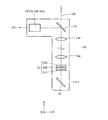
以下、実施形態を添付図面に基づいて説明する。図1は、実施形態にかかる露光装置の構成を概略的に示す図である。図1において、感光性基板であるウェハWの転写面(露光面)の法線方向に沿ってZ軸を、ウェハWの転写面内において図1の紙面に平行な方向にY軸を、ウェハWの転写面内において図1の紙面に垂直な方向にX軸をそれぞれ設定している。 Hereinafter, embodiments will be described with reference to the accompanying drawings. FIG. 1 is a view schematically showing a configuration of an exposure apparatus according to the embodiment. In FIG. 1, the Z-axis is along the normal direction of the transfer surface (exposure surface) of the wafer W, which is a photosensitive substrate, and the Y-axis is in the direction parallel to the paper surface of FIG. In the W transfer surface, the X axis is set in a direction perpendicular to the paper surface of FIG.
図1を参照すると、本実施形態の露光装置では、光源LSから露光光(照明光)が供給される。光源LSとして、たとえば193nmの波長のパルス光を供給するArFエキシマレーザ光源や、248nmの波長のパルス光を供給するKrFエキシマレーザ光源などを用いることができる。光源LSは、露光装置本体EXが収容されている筐体とは異なる筐体内に収容されている。光源LSから−Y方向に射出された光は、伝送光学系1を介して、露光装置本体EX内の空間光変調器2に入射する。
Referring to FIG. 1, in the exposure apparatus of the present embodiment, exposure light (illumination light) is supplied from a light source LS. As the light source LS, for example, an ArF excimer laser light source that supplies pulsed light with a wavelength of 193 nm, a KrF excimer laser light source that supplies pulsed light with a wavelength of 248 nm, or the like can be used. The light source LS is accommodated in a housing different from the housing in which the exposure apparatus main body EX is accommodated. Light emitted from the light source LS in the −Y direction is incident on the spatial
空間光変調器2は、後述するように、所定面内に配列されて個別に制御される複数のミラー要素と、露光装置の動作を統括的に制御する制御系CRからの制御信号に基づいて複数のミラー要素の姿勢を個別に制御駆動する駆動部とを有する。空間光変調器2の複数のミラー要素の配列面(以下、「空間光変調器の配列面」という)は、伝送光学系1を含む照明光学系(1〜7)の照明瞳に瞳強度分布を形成するために入射光に角度分布を付与する作用面として機能する。
As will be described later, the spatial
伝送光学系1は、図2に示すように、光源LSからの光の入射順に、光路折曲げミラー11、オプティカルインテグレータ12、リレー光学系13、およびビームスプリッター14を備えている。光路折曲げミラー11で+Z方向へ反射された光は、光軸AXの方向に間隔を隔てて配置された3つの光学部材121,122および123からなる波面分割型のオプティカルインテグレータ12に入射する。オプティカルインテグレータ12は、後述するように、XY平面に沿って並列配置された複数の波面分割要素により構成されている。オプティカルインテグレータ12の具体的な構成および作用については後述する。
As illustrated in FIG. 2, the transmission
オプティカルインテグレータ12に入射した光束は、複数の波面分割要素により二次元的に分割され、オプティカルインテグレータ12の後側焦点位置またはその近傍に複数の小光源を形成する。オプティカルインテグレータ12により形成された複数の小光源からの光は、前側レンズ群13aと後側レンズ群13bとからなるリレー光学系13を介して、空間光変調器2の配列面(作用面)を重畳的に照明する。光源LSとして、193nmの波長の光を供給するArFエキシマレーザ光源を用いる場合、オプティカルインテグレータ12を構成する3つの光学部材121〜123を例えば蛍石により形成しても良い。
The light beam incident on the
オプティカルインテグレータ12およびリレー光学系13を経た光は、ビームスプリッター14に入射する。ビームスプリッター14を透過した光は、上述したように、空間光変調器2に入射する。ビームスプリッター14で反射された光、すなわちビームスプリッター14により照明光路から取り出された光は、ビームモニター15に入射する。ビームモニター15は、照明光路から取り出された光に基づいて、空間光変調器2へ入射する光の配列面内の位置、空間光変調器2へ入射する光の配列面に対する角度、および空間光変調器2の配列面における光強度分布を計測する。
The light that has passed through the
ビームモニター15の計測結果は、制御系CRへ供給される。制御系CRは、ビームモニター15の出力に基づいて、伝送光学系1および空間光変調器2を制御する。ビームモニター15は、位置モニター15aと、角度モニター15bと、強度分布モニター15cとを備えている。位置モニター15aは、空間光変調器2の配列面における光の入射位置を計測する。角度モニター15bは、空間光変調器2へ入射する光の配列面における光の入射角度を計測する。
The measurement result of the beam monitor 15 is supplied to the control system CR. The control system CR controls the transmission
強度分布モニター15cは、空間光変調器2の配列面における光強度分布を計測する。位置モニター15aおよび強度分布モニター15cは、空間光変調器2の配列面と光学的にほぼ共役な位置に配置された光電変換面を有する撮像部を備えている。角度モニター15bは、空間光変調器2の配列面に対してほぼ光学的にフーリエ変換となる位置に配置された光電変換面を有する撮像部を備えている。ビームモニター15の内部構成は、例えば米国特許公開第2011/0069305号公報に開示されている。
The intensity distribution monitor 15 c measures the light intensity distribution on the arrangement surface of the spatial
リレー光学系13は、オプティカルインテグレータ12の後側焦点位置とリレー光学系13の前側焦点位置とがほぼ一致し、且つリレー光学系13の後側焦点位置と空間光変調器2の配列面の位置とがほぼ一致するように配置されている。その結果、オプティカルインテグレータ12により形成された各小光源からの光は、リレー光学系13を介してほぼ平行光となり、空間光変調器2の配列面に入射する。
In the relay
再び図1を参照すると、空間光変調器2から+Y方向へ射出された光は、リレーレンズ3を介して、マイクロフライアイレンズ(またはフライアイレンズ)4に入射する。リレーレンズ3は、その前側焦点位置が空間光変調器2の配列面の近傍に位置し、且つその後側焦点位置がマイクロフライアイレンズ4の入射面の近傍に位置しており、空間光変調器2の配列面とマイクロフライアイレンズ4の入射面とを光学的にフーリエ変換の関係に設定している。したがって、空間光変調器2を経た光は、後述するように、複数のミラー要素の姿勢に応じた光強度となるようにマイクロフライアイレンズ4の入射面に可変的に分布する。
Referring again to FIG. 1, the light emitted from the spatial
マイクロフライアイレンズ4は、たとえば縦横に且つ稠密に配列された多数の正屈折力を有する微小レンズからなる光学素子であり、平行平面板にエッチング処理を施して微小レンズ群を形成することによって構成されている。マイクロフライアイレンズでは、互いに隔絶されたレンズエレメントからなるフライアイレンズとは異なり、多数の微小レンズ(微小屈折面)が互いに隔絶されることなく一体的に形成されている。しかしながら、レンズ要素が縦横に配置されている点でマイクロフライアイレンズはフライアイレンズと同じ波面分割型のオプティカルインテグレータである。
The micro fly's
マイクロフライアイレンズ4における単位波面分割面としての矩形状の微小屈折面は、マスクM上において形成すべき照野の形状(ひいてはウェハW上において形成すべき露光領域の形状)と相似な矩形状である。なお、マイクロフライアイレンズ4として、例えばシリンドリカルマイクロフライアイレンズを用いることもできる。シリンドリカルマイクロフライアイレンズの構成および作用は、例えば米国特許第6913373号明細書に開示されている。
A rectangular minute refracting surface as a unit wavefront dividing surface in the micro fly's
第2のオプティカルインテグレータとしてのマイクロフライアイレンズ4に入射した光束は多数の微小レンズにより二次元的に分割され、その後側焦点面またはその近傍の照明瞳には、入射面に形成される光強度分布とほぼ同じ光強度分布を有する二次光源(多数の小光源からなる実質的な面光源:瞳強度分布)が形成される。マイクロフライアイレンズ4の直後の照明瞳に形成された二次光源からの光は、コンデンサー光学系5を介して、マスクブラインド6を重畳的に照明する。
The light beam incident on the micro fly's
こうして、照明視野絞りとしてのマスクブラインド6には、マイクロフライアイレンズ4の矩形状の微小屈折面の形状と焦点距離とに応じた矩形状の照野が形成される。なお、マイクロフライアイレンズ4の後側焦点面またはその近傍に、すなわち後述する投影光学系PLの入射瞳面と光学的にほぼ共役な位置に、二次光源に対応した形状の開口部(光透過部)を有する照明開口絞りを配置してもよい。
Thus, a rectangular illumination field corresponding to the shape and focal length of the rectangular micro-refractive surface of the micro fly's
マスクブラインド6の矩形状の開口部(光透過部)を介した光束は、結像光学系7の集光作用を受け、且つ結像光学系7の光路中に配置された光路折曲げミラーにより−Z方向へ反射された後、所定のパターンが形成されたマスクMを重畳的に照明する。すなわち、結像光学系7は、マスクブラインド6の矩形状開口部の像をマスクM上に形成することになる。 The light beam that has passed through the rectangular opening (light transmitting portion) of the mask blind 6 is subjected to the condensing action of the imaging optical system 7 and is reflected by the optical path bending mirror disposed in the optical path of the imaging optical system 7. After being reflected in the −Z direction, the mask M on which a predetermined pattern is formed is illuminated in a superimposed manner. That is, the imaging optical system 7 forms an image of the rectangular opening of the mask blind 6 on the mask M.
マスクステージMS上に保持されたマスクMを透過した光束は、投影光学系PLを介して、ウェハステージWS上に保持されたウェハ(感光性基板)W上にマスクパターンの像を形成する。こうして、投影光学系PLの光軸AXと直交する平面(XY平面)内においてウェハステージWSを二次元的に駆動制御しながら、ひいてはウェハWを二次元的に駆動制御しながら一括露光またはスキャン露光を行うことにより、ウェハWの各露光領域にはマスクMのパターンが順次露光される。 The light beam transmitted through the mask M held on the mask stage MS forms an image of a mask pattern on the wafer (photosensitive substrate) W held on the wafer stage WS via the projection optical system PL. In this way, batch exposure or scan exposure is performed while the wafer stage WS is two-dimensionally driven and controlled in a plane (XY plane) orthogonal to the optical axis AX of the projection optical system PL, and thus the wafer W is two-dimensionally driven and controlled. As a result, the pattern of the mask M is sequentially exposed in each exposure region of the wafer W.
本実施形態の露光装置は、伝送光学系1を含む照明光学系(1〜7)を介した光に基づいて照明光学系の射出瞳面における瞳強度分布を計測する第1瞳強度分布計測部DTrと、投影光学系PLを介した光に基づいて投影光学系PLの瞳面(投影光学系PLの射出瞳面)における瞳強度分布を計測する第2瞳強度分布計測部DTwと、第1および第2瞳強度分布計測部DTr,DTwのうちの少なくとも一方の計測結果に基づいて空間光変調器2を制御し且つ露光装置の動作を統括的に制御する制御系CRとを備えている。
The exposure apparatus of the present embodiment is a first pupil intensity distribution measurement unit that measures the pupil intensity distribution on the exit pupil plane of the illumination optical system based on light via the illumination optical system (1-7) including the transmission
第1瞳強度分布計測部DTrは、例えば照明光学系の射出瞳位置と光学的に共役な位置に配置された光電変換面を有する撮像部を備え、照明光学系による被照射面上の各点に関する瞳強度分布(各点に入射する光が照明光学系の射出瞳位置に形成する瞳強度分布)を計測する。また、第2瞳強度分布計測部DTwは、例えば投影光学系PLの瞳位置と光学的に共役な位置に配置された光電変換面を有する撮像部を備え、投影光学系PLの像面の各点に関する瞳強度分布(各点に入射する光が投影光学系PLの瞳位置に形成する瞳強度分布)を計測する。 The first pupil intensity distribution measurement unit DTr includes, for example, an imaging unit having a photoelectric conversion surface disposed at a position optically conjugate with the exit pupil position of the illumination optical system, and each point on the surface to be irradiated by the illumination optical system. Is measured (pupil intensity distribution formed at the exit pupil position of the illumination optical system by the light incident on each point). In addition, the second pupil intensity distribution measurement unit DTw includes an imaging unit having a photoelectric conversion surface arranged at a position optically conjugate with the pupil position of the projection optical system PL, for example, and includes each image plane of the projection optical system PL. A pupil intensity distribution related to the points (pupil intensity distribution formed by light incident on each point at the pupil position of the projection optical system PL) is measured.
第1および第2瞳強度分布計測部DTr,DTwの詳細な構成および作用については、例えば米国特許公開第2008/0030707号明細書を参照することができる。また、瞳強度分布計測部として、米国特許公開第2010/0020302号公報の開示を参照することもできる。 For the detailed configuration and operation of the first and second pupil intensity distribution measuring units DTr and DTw, reference can be made to, for example, US Patent Publication No. 2008/0030707. As the pupil intensity distribution measuring unit, the disclosure of US Patent Publication No. 2010/0020302 can be referred to.
本実施形態では、マイクロフライアイレンズ4により形成される二次光源を光源として、照明光学系の被照射面に配置されるマスクM(ひいてはウェハW)をケーラー照明する。このため、二次光源が形成される位置は投影光学系PLの開口絞りASの位置と光学的に共役であり、二次光源の形成面を照明光学系の照明瞳面と呼ぶことができる。また、この二次光源の形成面の像を照明光学系の射出瞳面と呼ぶことができる。典型的には、照明瞳面に対して被照射面(マスクMが配置される面、または投影光学系PLを含めて照明光学系と考える場合にはウェハWが配置される面)が光学的なフーリエ変換面となる。瞳強度分布とは、照明光学系の照明瞳面または当該照明瞳面と光学的に共役な面における光強度分布(輝度分布)である。
In this embodiment, the secondary light source formed by the micro fly's
マイクロフライアイレンズ4による波面分割数が比較的大きい場合、マイクロフライアイレンズ4の入射面に形成される大局的な光強度分布と、二次光源全体の大局的な光強度分布(瞳強度分布)とが高い相関を示す。このため、マイクロフライアイレンズ4の入射面および当該入射面と光学的に共役な面も照明瞳面と呼ぶことができ、これらの面における光強度分布についても瞳強度分布と称することができる。図1の構成において、リレーレンズ3およびマイクロフライアイレンズ4は、空間光変調器2を経た光束に基づいてマイクロフライアイレンズ4の直後の照明瞳に瞳強度分布を形成する分布形成光学系を構成している。
When the number of wavefront divisions by the micro fly's
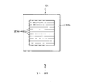
次に、空間光変調器2の構成および作用を具体的に説明する。空間光変調器2は、図3に示すように、所定面内に配列された複数のミラー要素2aと、複数のミラー要素2aを保持する基盤2bと、基盤2bに接続されたケーブル(不図示)を介して複数のミラー要素2aの姿勢を個別に制御駆動する駆動部2cとを備えている。図3では、空間光変調器2からマイクロフライアイレンズ4の入射面4aまでの光路を示している。
Next, the configuration and operation of the spatial
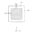
空間光変調器2では、制御系CRからの指令に基づいて作動する駆動部2cの作用により、複数のミラー要素2aの姿勢がそれぞれ変化し、各ミラー要素2aがそれぞれ所定の向きに設定される。空間光変調器2は、図4に示すように、二次元的に配列された複数の微小なミラー要素2aを備え、入射した光に対して、その入射位置に応じた空間的な変調を可変的に付与して射出する。説明および図示を簡単にするために、図3および図4では空間光変調器2が4×4=16個のミラー要素2aを備える構成例を示しているが、実際には16個よりもはるかに多数、典型的には4000個〜100,000個程度のミラー要素2aを備えている。
In the spatial
図3を参照すると、空間光変調器2に入射する光線群のうち、光線L1は複数のミラー要素2aのうちのミラー要素SEaに、光線L2はミラー要素SEaとは異なるミラー要素SEbにそれぞれ入射する。同様に、光線L3はミラー要素SEa,SEbとは異なるミラー要素SEcに、光線L4はミラー要素SEa〜SEcとは異なるミラー要素SEdにそれぞれ入射する。ミラー要素SEa〜SEdは、その位置に応じて設定された空間的な変調を光L1〜L4に与える。
Referring to FIG. 3, among the light beams incident on the spatial
空間光変調器2では、すべてのミラー要素2aの反射面が1つの平面に沿って設定された基準状態において、伝送光学系1の光軸AXと平行な方向に沿って入射した光線が、空間光変調器2で反射された後に、リレーレンズ3の光軸AXと平行な方向に進むように構成されている。また、上述したように、空間光変調器2の複数のミラー要素2aの配列面とマイクロフライアイレンズ4の入射面4aとは、リレーレンズ3を介して光学的にフーリエ変換の関係に位置決めされている。
In the spatial
したがって、空間光変調器2の複数のミラー要素SEa〜SEdによって反射されて所定の角度分布が与えられた光は、マイクロフライアイレンズ4の入射面4aに所定の光強度分布SP1〜SP4を形成する。すなわち、リレーレンズ3は、空間光変調器2の複数のミラー要素SEa〜SEdが射出光に与える角度を、空間光変調器2のファーフィールド(フラウンホーファー回折領域)である入射面4a上での位置に変換する。こうして、マイクロフライアイレンズ4が形成する二次光源の光強度分布(瞳強度分布)は、空間光変調器2およびリレーレンズ3がマイクロフライアイレンズ4の入射面4aに形成する光強度分布に対応した分布となる。
Therefore, light reflected by the plurality of mirror elements SEa to SEd of the spatial
空間光変調器2は、図4に示すように、平面状の反射面を上面にした状態で1つの平面に沿って規則的に且つ二次元的に配列された多数の微小な反射素子であるミラー要素2aを含む可動マルチミラーである。各ミラー要素2aは可動であり、その反射面の傾き、すなわち反射面の傾斜角および傾斜方向は、制御系CRからの制御信号に基づいて作動する駆動部2cの作用により独立に制御される。各ミラー要素2aは、その反射面に平行な二方向であって互いに直交する二方向を回転軸として、所望の回転角度だけ連続的或いは離散的に回転することができる。すなわち、各ミラー要素2aの反射面の傾斜を二次元的に制御することが可能である。
As shown in FIG. 4, the spatial
各ミラー要素2aの反射面を離散的に回転させる場合、回転角を複数の状態(例えば、・・・、−2.5度、−2.0度、・・・0度、+0.5度・・・+2.5度、・・・)で切り換え制御するのが良い。図4には外形が正方形状のミラー要素2aを示しているが、ミラー要素2aの外形形状は正方形に限定されない。ただし、光利用効率の観点から、ミラー要素2aの隙間が少なくなるように配列可能な形状(最密充填可能な形状)とすることができる。また、光利用効率の観点から、隣り合う2つのミラー要素2aの間隔を必要最小限に抑えることができる。
When the reflection surface of each
本実施形態では、空間光変調器2として、たとえば二次元的に配列された複数のミラー要素2aの向きを連続的にそれぞれ変化させる空間光変調器を用いている。このような空間光変調器として、たとえば欧州特許公開第779530号公報、米国特許第5,867,302号公報、米国特許第6,480,320号公報、米国特許第6,600,591号公報、米国特許第6,733,144号公報、米国特許第6,900,915号公報、米国特許第7,095,546号公報、米国特許第7,295,726号公報、米国特許第7,424,330号公報、米国特許第7,567,375号公報、米国特許公開第2008/0309901号公報、米国特許公開第2011/0181852号公報、並びに米国特許公開第2011/188017号公報に開示される空間光変調器を用いることができる。なお、二次元的に配列された複数のミラー要素2aの向きを離散的に複数の段階を持つように制御してもよい。
In the present embodiment, as the spatial
空間光変調器2では、制御系CRからの制御信号に応じて作動する駆動部2cの作用により、複数のミラー要素2aの姿勢がそれぞれ変化し、各ミラー要素2aがそれぞれ所定の向きに設定される。空間光変調器2の複数のミラー要素2aによりそれぞれ所定の角度で反射された光は、リレーレンズ3による光学的なフーリエ変換作用により、マイクロフライアイレンズ4の入射面4aに(照明瞳に)、ひいてはマイクロフライアイレンズ4の直後の照明瞳に、所望の瞳強度分布を形成する。
In the spatial
さらに、マイクロフライアイレンズ4の直後の照明瞳と光学的に共役な別の照明瞳の位置、すなわち結像光学系7の瞳位置および投影光学系PLの瞳位置(開口絞りASが配置されている位置)にも、所望の瞳強度分布が形成される。このように、空間光変調器2は、マイクロフライアイレンズ4の直後の照明瞳に瞳強度分布を可変的に形成する。リレーレンズ3は、空間光変調器2からの射出光束の角度方向の分布を、分布形成光学系からの射出光束の断面における位置分布に変換する。
Further, the position of another illumination pupil optically conjugate with the illumination pupil immediately after the micro fly's
本実施形態において、制御部CRには、必要に応じて、ビームモニター15の強度分布モニター15cから、空間光変調器2の配列面における光強度分布の計測結果が供給される。この場合、制御部CRは、強度分布モニター15cの光強度分布に関する計測結果を随時参照し、光源LSから供給される光のビームプロファイルの経時的な変動に応じて空間光変調器2を適宜制御することにより、所望の瞳強度分布を安定的に形成する。
In this embodiment, the measurement result of the light intensity distribution on the arrangement surface of the spatial
また、制御部CRは、位置モニター15aの出力を参照して空間光変調器2の作用面へ入射する光束の位置変動を位置調整部材により微調整し、角度モニター15bの出力を参照して空間光変調器2の作用面へ入射する光束の角度変動を角度調整部材により微調整する。位置調整部材および角度調整部材として、例えばリレー光学系13の前側レンズ群13aとビームスプリッター14との間の光路中に配置された一対の電動チルトミラー(不図示)を用いることができる。
Further, the controller CR finely adjusts the position fluctuation of the light beam incident on the working surface of the spatial
露光装置本体EX、すなわち空間光変調器2からウェハステージWSへ至る部分は、全体的にかなり大きな装置であり、設置のための所要床面積は大きい。また、露光装置に露光光(照明光)を供給する光源LSとして用いられるArFエキシマレーザ光源(またはKrFエキシマレーザ光源)もかなり大きな装置である。したがって、エキシマレーザ光源を用いる露光装置では、光源LSを露光装置本体(EX;2〜WS)からある程度離間させて配置することが多い。
The exposure apparatus main body EX, that is, the part from the spatial
一例として、光源LSが設置される階の上階に露光装置本体(EX;2〜WS)を設置し、光源LSの光出力口から射出された光を、伝送光学系1を介して、露光装置本体(EX;2〜WS)の光取入口に配置された空間光変調器2の配列面(作用面)まで導く場合もある。すなわち、光源LSの光出力口から空間光変調器2の配列面までの光路は比較的長い。
As an example, an exposure apparatus body (EX; 2 to WS) is installed on the upper floor where the light source LS is installed, and light emitted from the light output port of the light source LS is exposed via the transmission
本実施形態の伝送光学系1では、オプティカルインテグレータ12により波面分割された複数の部分光束が、リレー光学系13を介して、空間光変調器2の配列面(作用面)で重畳される。したがって、光源LSから射出された不均一なビームプロファイルを有する光が、オプティカルインテグレータ12の作用により強度分布の均一性が向上した光となって、空間光変調器2の配列面へ入射する。すなわち、オプティカルインテグレータ12の平滑化作用により、空間光変調器2の各ミラー要素2aへ入射する光束の光強度分布が均一化され、ひいては各ミラー要素2aから射出される光束の光強度分布も均一化される。
In the transmission
ここで、オプティカルインテグレータ12に入射する光束の光束断面における強度分布よりも空間光変調器2の配列面に達する光束の光束断面における強度分布の方が均一性が良い場合、配列面においてほぼ均一な強度分布であるとみなすことができる。なお、均一性の評価尺度としては、光束断面内での強度分布のPV値(peak to valley value:最大値と最小値との差)、RMS(root mean square:自乗平均平方根)、標準偏差、またはコントラスト(最大強度をImax、最小強度をIminとするとき、(Imax−Imin)/(Imax+Imin)またはImax/Imin)などを用いることができる。
Here, when the intensity distribution in the light beam cross section of the light beam reaching the array surface of the spatial
しかしながら、オプティカルインテグレータ12を経て波面分割された複数の部分光束を空間光変調器2の配列面で重畳させると、光源の空間的コヒーレンシーが比較的高い場合、空間光変調器2の配列面上で干渉縞が発生する恐れがある。干渉縞の分布は光源LSの出力分布の変化に敏感に反応するため、空間光変調器2の配列面での光束の光強度分布の均一化に悪影響を及ぼし、ひいては所望の瞳強度分布を安定的に形成することが困難になる。
However, if a plurality of partial light beams that have been wavefront-divided through the
上述したように、オプティカルインテグレータ12の複数の波面分割要素を経た複数の部分光束は、空間光変調器2の配列面で重畳される。このため、互いに隣り合う2つの波面分割要素を経た部分光束は、空間光変調器2の配列面上で干渉縞を形成する。ただし、エキシマレーザ光源のような光源LSでは、空間的コヒーレンシーがそれほど高くないので、互いに離れた2つの波面分割要素を経た部分光束は、空間光変調器2の配列面上で干渉縞をほとんど形成しない(すなわちコントラストの小さい干渉縞しか形成しない)。
As described above, the plurality of partial light beams that have passed through the plurality of wavefront splitting elements of the
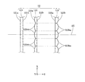
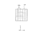
図5は、伝送光学系の光路中に配置されたオプティカルインテグレータのYZ平面に沿った断面図である。図6は、オプティカルインテグレータのXZ平面に沿った断面図である。図7は、オプティカルインテグレータを構成する第1光学部材の入射側の面を光軸に沿って光源側から見た図である。図8は、オプティカルインテグレータを構成する第2光学部材の入射側の面を光軸に沿って光源側から見た図である。 FIG. 5 is a cross-sectional view taken along the YZ plane of the optical integrator disposed in the optical path of the transmission optical system. FIG. 6 is a cross-sectional view of the optical integrator along the XZ plane. FIG. 7 is a view of the incident-side surface of the first optical member constituting the optical integrator as viewed from the light source side along the optical axis. FIG. 8 is a view of the incident side surface of the second optical member constituting the optical integrator as viewed from the light source side along the optical axis.
図9は、オプティカルインテグレータを構成する第3光学部材の射出面を光軸に沿って空間光変調器側から見た図である。図5および図6を参照すると、オプティカルインテグレータ12は、光の入射側(光源LS側)から順に、第1光学部材121と、第2光学部材122と、第3光学部材123とを備えている。光学部材121〜123は、全体的に平行平面板の形態を有し、光軸AXに沿って間隔を隔てて配置されている。
FIG. 9 is a view of the exit surface of the third optical member constituting the optical integrator as viewed from the spatial light modulator side along the optical axis. Referring to FIGS. 5 and 6, the
第1光学部材121は、図5、図6および図7に示すように、複数の円筒面状の単位的な光学面121aaがY方向に並んで配置された入射側の面121aと、光軸AX(Z方向)と直交する平面状の射出面121bとを有する。具体的に、光学面121aaは、光の入射側に凸面を向けた円筒面状であって、YZ平面において曲率を有するが、XZ平面において曲率を有しない。換言すれば、光学面121aaは、Y方向に関して正の屈折力を有するが、X方向に関して屈折力を有しない。Y方向に沿って互いに隣り合う2つの光学面121aaの境界線は、X方向に沿って直線状に延びている。
As shown in FIGS. 5, 6, and 7, the first
第2光学部材122は、図5、図6および図8に示すように、複数の円筒面状の単位的な光学面122aaがX方向に並んで配置された入射側の面122aと、光軸AXと直交する平面状の射出面122bとを有する。具体的に、光学面122aaは、光の入射側に凸面を向けた円筒面状であって、XZ平面において曲率を有するが、YZ平面において曲率を有しない。換言すれば、光学面122aaは、X方向に関して正の屈折力を有するが、Y方向に関して屈折力を有しない。X方向に沿って互いに隣り合う2つの光学面122aaの境界線は、Y方向に沿って直線状に延びている。
As shown in FIGS. 5, 6, and 8, the second
第3光学部材123は、図5、図6および図9に示すように、光軸AXと直交する平面状の入射側の面123aと、複数のトーリック面状の単位的な光学面123baがX方向およびY方向に沿って縦横に隣接配置された射出面123bとを有する。具体的に、光学面123baは光の射出側(空間光変調器2側)に凸面を向けたトーリック面状であって、そのYZ平面における曲率とXZ平面における曲率とは互いに異なる。換言すれば、光学面123baのY方向に関する屈折力(すなわちYZ平面における屈折力)とX方向に関する屈折力(すなわちXZ平面における屈折力)とは互いに異なる。
As shown in FIGS. 5, 6, and 9, the third
光学面123baは、図9に示すように、X方向に沿った一辺とY方向に沿った一辺とにより規定される矩形状の外形を有する。オプティカルインテグレータ12は、図5および図6において破線で示すように、光軸AXの方向(Z方向)に沿って見たときに、複数の光学面121aaのX方向に沿って直線状に延びる境界線と複数の光学面123baのX方向に沿って直線状に延びる境界線とが互いに重なり合い、且つ複数の光学面122aaのY方向に沿って直線状に延びる境界線と複数の光学面123baのY方向に沿って直線状に延びる境界線とが互いに重なり合うように構成されている。
As shown in FIG. 9, the optical surface 123ba has a rectangular outer shape defined by one side along the X direction and one side along the Y direction. The
すなわち、オプティカルインテグレータ12では、1つの光学面123baを射出面として光源LS側へZ方向に沿って対応する光学面121aaまで直線的に延びる直方体状の部分が、単位的な波面分割要素を構成している。したがって、オプティカルインテグレータ12を構成する各波面分割要素は、X方向に沿った一辺とY方向に沿った一辺とにより規定される矩形状の断面を有する。なお、図5〜図9では、図面の明瞭化のために、オプティカルインテグレータを構成する波面分割要素の数を実際よりも少なく表わしている。
That is, in the
このように、本実施形態では、オプティカルインテグレータ12を構成する各波面分割要素は、Y方向に関して正の屈折力を有する円筒面状の光学面121aaと、光学面121aaよりも後側(空間光変調器2側)に間隔を隔てて配置されてX方向に関して正の屈折力を有する円筒面状の光学面122aaと、光学面122aaよりも後側に間隔を隔てて配置されてY方向に関して正の屈折力を有し且つX方向に関して正の屈折力を有する光学面123baとを有する。
Thus, in this embodiment, each wavefront splitting element constituting the
また、本実施形態では、オプティカルインテグレータ12のY方向に関する焦点距離(すなわちYZ平面における焦点距離)は、X方向に関する焦点距離(すなわちXZ平面における焦点距離)よりも大きい。ここで、オプティカルインテグレータ12のY方向に関する焦点距離は、光学面121aaのY方向に関する正の屈折力と、光学面123baのY方向に関する正の屈折力と、光学面121aaと光学面123baとの光軸AXに沿った間隔とに依存する。一方、オプティカルインテグレータ12のX方向に関する焦点距離は、光学面122aaのX方向に関する正の屈折力と、光学面123baのX方向に関する正の屈折力と、光学面122aaと光学面123baとの光軸AXに沿った間隔とに依存する。
In the present embodiment, the focal length in the Y direction of the optical integrator 12 (that is, the focal length in the YZ plane) is larger than the focal length in the X direction (that is, the focal length in the XZ plane). Here, the focal length in the Y direction of the
本実施形態のオプティカルインテグレータ12では、光学面121aaと光学面122aaとが光軸AXに沿って互いに異なる位置に配置され、光学面123baのY方向に関する屈折力とX方向に関する屈折力とが互いに異なり、且つ光学面121aaと光学面123baとの間隔と光学面122aaと光学面123baとの間隔とが互いに異なっている。その結果、オプティカルインテグレータ12のY方向に関する後側焦点位置とX方向に関する後側焦点位置とを光軸AX方向に沿って大きく離間させることなく、Y方向に関する焦点距離がX方向に関する焦点距離よりも所要量だけ大きくなるようにオプティカルインテグレータ12を設計することは容易である。
In the
また、本実施形態のオプティカルインテグレータ12では、そのY方向に関する後側焦点位置およびX方向に関する後側焦点位置が、第3光学部材123の射出面を構成する光学面123baよりも後側(空間光変調器2側)に位置している。そして、オプティカルインテグレータ12のY方向に関する後側焦点位置は、X方向に関する後側焦点位置にあるか、あるいはX方向に関する後側焦点位置よりも後側に位置している。この構成により、第3光学部材123の照射エネルギによる損傷を回避することができる。一方、オプティカルインテグレータ12のY方向に関する前側焦点位置は第1光学部材121の入射側の面を構成する光学面121aaの位置にあり、X方向に関する前側焦点位置は第2光学部材122の入射側の面を構成する光学面122aaの位置にある。
Further, in the
以下、本実施形態のオプティカルインテグレータ12の具体的な作用の説明に先立って、通常の設計にしたがう比較例における不都合について説明する。通常の設計では、空間光変調器2の配列面がYZ平面において傾いているため、X方向に細長い矩形状の断面を有する光束を空間光変調器2に入射させる。これに対応して、図10に示すようにX方向に沿って細長い矩形状の断面を有する複数の波面分割要素101aをX方向およびY方向に沿って並列的に隣接配置することによりオプティカルインテグレータ101を構成している。
Hereinafter, prior to the description of the specific operation of the
すなわち、空間光変調器2に入射させるべき光束の断面の外形形状と、空間光変調器2への入射光束の平滑化のためのオプティカルインテグレータ101を構成する各波面分割要素101aの断面の外形形状とは相似である。そして、例えばエキシマレーザ光源を用いる構成では、オプティカルインテグレータ101に入射する光束において、矩形状の波面分割要素101aの短辺方向であるY方向に関する空間的コヒーレンシーの方が、波面分割要素101aの長辺方向であるX方向に関する空間的コヒーレンシーよりも大きい。
That is, the outer shape of the cross section of the light beam to be incident on the spatial
この場合、複数の波面分割要素101aにおけるY方向ピッチの方がX方向ピッチよりも小さく且つY方向に関する空間的コヒーレンシーの方がX方向に関する空間的コヒーレンシーよりも大きいため、Y方向に沿って互いに隣り合う2つの波面分割要素101aを経た部分光束は空間光変調器2の配列面上で干渉縞を形成し易い。そこで、Y方向に沿って互いに隣り合う2つの波面分割要素を経た部分光束による干渉縞の形成を低減する(干渉縞のコントラストを低減する)ために、図11に示すように波面分割要素101aを相似的に拡大させて得られる外形形状の波面分割要素102aをX方向およびY方向に沿って並列的に隣接配置することによりオプティカルインテグレータ102を構成する手法が考えられる。
In this case, since the Y direction pitch in the plurality of
図11に示す手法では、Y方向に沿って互いに隣り合う2つの波面分割要素を経た部分光束による干渉縞の形成を低減することができ、且つX方向に細長い所望の矩形状断面を有する光束を空間光変調器2に入射させることができる。しかしながら、オプティカルインテグレータ102を構成する波面分割要素102aの数が減少した分だけ平滑化効果が小さくなり、ひいては空間光変調器2の各ミラー要素2aへ入射する光束の光強度分布を均一化することが困難になる。
In the method shown in FIG. 11, the formation of interference fringes due to partial light fluxes that have passed through two wavefront splitting elements adjacent to each other along the Y direction can be reduced, and a light flux having a desired rectangular cross section elongated in the X direction. The light can enter the spatial
本実施形態のオプティカルインテグレータ12では、図12に示すように、空間的コヒーレンシーの高いY方向にのみ波面分割要素101aを拡大させて得られる外形形状の波面分割要素12aをX方向およびY方向に沿って並列的に隣接配置している。換言すれば、オプティカルインテグレータ12を構成する各波面分割要素12aの断面の外形形状は、空間光変調器2に入射させるべき光束の断面の外形形状と相似ではない。
In the
オプティカルインテグレータ12では、空間的コヒーレンシーの高いY方向に沿った波面分割要素12aのピッチを拡大しているので、Y方向に沿って互いに隣り合う2つの波面分割要素を経た部分光束による干渉縞の形成を低減することができる。しかも、図10と図12とを比較して明らかなように、一列に並ぶ波面分割要素の数を多く確保し難いX方向ではなく確保し易いY方向にのみ波面分割要素12aのピッチを拡大しているので、平滑化効果は実質的に損なわれることがない。
In the
ただし、通常の設計にしたがってオプティカルインテグレータ12のY方向に関する焦点距離とX方向に関する焦点距離とを互いに同じに設定すると、X方向に細長い所望の矩形状断面を有する光束を空間光変調器2に入射させることができない。本実施形態のオプティカルインテグレータ12では、上述したようにY方向に関する焦点距離がX方向に関する焦点距離よりも所要量だけ大きくなるように構成することにより、X方向に細長い所望の矩形状断面を有する光束を空間光変調器2に入射させることを可能にしている。
However, if the focal length in the Y direction and the focal length in the X direction of the
ちなみに、矩形状の波面分割要素12aのX方向に沿った寸法およびY方向に沿った寸法をExおよびEy(図12を参照)とし、オプティカルインテグレータ12のX方向に関する焦点距離およびY方向に関する焦点距離をFoxおよびFoyとし、リレー光学系13の焦点距離をFrとし、空間光変調器2への入射光束の矩形状断面のX方向に沿った寸法およびY方向に沿った寸法をSxおよびSyとすると、次の式(1)および(2)に示す関係が成立する。
Sx=Ex×(Fr/Fox) (1)
Sy=Ey×(Fr/Foy) (2)
Incidentally, the dimension along the X direction and the dimension along the Y direction of the rectangular
Sx = Ex × (Fr / Fox) (1)
Sy = Ey × (Fr / Foy) (2)
上述したように、本実施形態のオプティカルインテグレータ12は、Y方向に関する空間的コヒーレンシーの方がX方向に関する空間的コヒーレンシーよりも大きい光束が入射するように配置され、そのY方向に関する焦点距離はX方向に関する焦点距離よりも大きく設定されている。その結果、平滑化効果を実質的に損なうことなくY方向に沿って互いに隣り合う2つの波面分割要素を経た部分光束による干渉縞の形成を低減することと、X方向に細長い所望の矩形状断面を有する光束を空間光変調器2に入射させることとを両立させることができる。
As described above, the
こうして、本実施形態の伝送光学系1では、オプティカルインテグレータ12により空間光変調器2の各ミラー要素2aへ入射する光束の光強度分布の均一化を図るとともに、互いに隣り合う2つの波面分割要素12aを経た部分光束による干渉縞の形成を低減することができ、ひいては光源LSの出力分布が変化してもほぼ均一な強度分布を有する光束を空間光変調器2の作用面へ安定的に導くことができる。その結果、瞳強度分布の形成に際して多数のミラー要素2aを駆動すべき空間光変調器2の制御性が向上する。
Thus, in the transmission
本実施形態の照明光学系(1〜7)では、光源LSの出力分布が変化してもほぼ均一な強度分布を有する光束を空間光変調器2の作用面へ安定的に導く伝送光学系1を用いて、マイクロフライアイレンズ4の直後の照明瞳に、所望の瞳強度分布を安定的に形成することができる。本実施形態の露光装置(1〜WS)では、所望の瞳強度分布を安定的に形成する照明光学系(1〜7)を用いて、転写すべきマスクMのパターンの特性に応じて実現された適切な照明条件のもとで、微細パターンをウェハWに正確に転写することができる。
In the illumination optical system (1-7) of the present embodiment, the transmission
なお、上述の説明では、伝送光学系1において、図5〜図9に示す特定の構成を有するオプティカルインテグレータ12を用いている。しかしながら、これに限定されることなく、伝送光学系に配置されるオプティカルインテグレータの具体的な構成については様々な変形例が可能である。一例として、第1光学部材121の入射側の面121aには複数の円筒面状の光学面121aaがY方向に並んで配置されているが、これに限定されることなく、第1光学部材の射出面に複数の円筒面状の光学面を配置しても良い。
In the above description, the transmission
また、光学面121aaは光の入射側に凸面を向けた円筒面状であって、YZ平面において曲率を有するが、XZ平面において曲率を有しない。しかしながら、これに限定されることなく、第1光学部材の入射側の面または射出面に配置される円筒面状の光学面が、X方向に関して小さい屈折力を有していても良い。 The optical surface 121aa has a cylindrical shape with a convex surface facing the light incident side, and has a curvature in the YZ plane, but has no curvature in the XZ plane. However, the present invention is not limited to this, and the cylindrical optical surface disposed on the incident side surface or the exit surface of the first optical member may have a small refractive power in the X direction.
また、第2光学部材122の入射側の面122aには、複数の円筒面状の光学面122aaがX方向に並んで配置されている。しかしながら、これに限定されることなく、第2光学部材の射出面に複数の円筒面状の光学面を配置しても良い。また、光学面122aaは光の入射側に凸面を向けた円筒面状であって、XZ平面において曲率を有するが、YZ平面において曲率を有しない。しかしながら、これに限定されることなく、第2光学部材の入射側の面または射出面に配置される円筒面状の光学面が、Y方向に関して小さい屈折力を有していても良い。
A plurality of cylindrical optical surfaces 122aa are arranged in the X direction on the
また、第3光学部材123の射出面123bには、複数のトーリック面状の光学面123baがX方向およびY方向に沿って縦横に隣接配置されている。しかしながら、これに限定されることなく、第3光学部材の入射側の面に複数のトーリック面状の光学面を配置しても良い。また、光学面123baは光の射出側に凸面を向けたトーリック面状であって、光学面123baのY方向に関する屈折力とX方向に関する屈折力とが互いに異なっている。しかしながら、これに限定されることなく、第3光学部材の入射側の面または射出面に配置される単位的な光学面のY方向に関する屈折力とX方向に関する屈折力とが互いに同じでも良い。
In addition, a plurality of toric surface-like optical surfaces 123ba are adjacently arranged vertically and horizontally along the X direction and the Y direction on the
本発明において重要なことは、オプティカルインテグレータを構成する各波面分割要素が、第1方向に関して正の屈折力を有する円筒面状の第1光学面と、第1光学面よりも後側に間隔を隔てて配置されて第1方向と交差する第2方向に関して正の屈折力を有する円筒面状の第2光学面と、第2光学面よりも後側に間隔を隔てて配置されて第1方向に関して正の屈折力を有し且つ第2方向に関して正の屈折力を有する第3光学面とを有し、オプティカルインテグレータの第1方向に関する焦点距離が第2方向に関する焦点距離よりも大きいことである。あるいは、オプティカルインテグレータが第1方向に関する空間的コヒーレンシーの方が第2方向に関する空間的コヒーレンシーよりも大きい光束が入射するように配置され、オプティカルインテグレータの第1方向に関する焦点距離が第2方向に関する焦点距離よりも大きいことである。 What is important in the present invention is that each wavefront splitting element constituting the optical integrator is spaced apart from the cylindrical first optical surface having a positive refractive power in the first direction and the rear side of the first optical surface. A second optical surface having a cylindrical surface having a positive refractive power with respect to a second direction that is spaced apart and intersects the first direction, and a first direction that is spaced apart from the second optical surface at a rear side. And a third optical surface having a positive refractive power with respect to the second direction and having a positive refractive power with respect to the second direction, and the focal length in the first direction of the optical integrator is greater than the focal length in the second direction. . Alternatively, the optical integrator is arranged so that the light beam having a larger spatial coherency in the first direction than the spatial coherency in the second direction is incident, and the focal length in the first direction of the optical integrator is the focal length in the second direction. Is bigger than that.
上述の実施形態では、二次元的に配列されて個別に制御される複数のミラー要素を有する空間光変調器として、二次元的に配列された複数の反射面の向き(角度:傾き)を個別に制御可能な空間光変調器2を用いている。しかしながら、これに限定されることなく、たとえば二次元的に配列された複数の反射面の高さ(位置)を個別に制御可能な空間光変調器を用いることもできる。このような空間光変調器としては、たとえば米国特許第5,312,513号公報、並びに米国特許第6,885,493号公報の図1dに開示される空間光変調器を用いることができる。これらの空間光変調器では、二次元的な高さ分布を形成することで回折面と同様の作用を入射光に与えることができる。なお、上述した二次元的に配列された複数の反射面を持つ空間光変調器を、たとえば米国特許第6,891,655号公報や、米国特許公開第2005/0095749号公報の開示に従って変形しても良い。
In the above-described embodiment, as the spatial light modulator having a plurality of mirror elements that are two-dimensionally arranged and individually controlled, the directions (angle: inclination) of the plurality of two-dimensionally arranged reflecting surfaces are individually set. The controllable spatial
上述の実施形態では、照明光学系(1〜7)の照明瞳に瞳強度分布を形成するために入射光に角度分布を付与する作用面を持つ光学部材として、作用面内で二次元的に配列された複数のミラー要素2aを有する反射型の空間光変調器2を用いている。しかしながら、これに限定されることなく、所定面内に配列されて個別に制御される複数の透過光学要素を備えた透過型の空間光変調器、回折光学面(作用面)を有する回折光学素子などを用いることもできる。
In the above-described embodiment, as an optical member having a working surface that imparts an angular distribution to incident light in order to form a pupil intensity distribution in the illumination pupil of the illumination optical system (1 to 7), two-dimensionally within the working surface. A reflective spatial
上述の実施形態では、マスクの代わりに、所定の電子データに基づいて所定パターンを形成する可変パターン形成装置を用いることができる。なお、可変パターン形成装置としては、たとえば所定の電子データに基づいて駆動される複数の反射素子を含む空間光変調素子を用いることができる。空間光変調素子を用いた露光装置は、たとえば米国特許公開第2007/0296936号公報に開示されている。また、上述のような非発光型の反射型空間光変調器以外に、透過型空間光変調器を用いても良く、自発光型の画像表示素子を用いても良い。 In the above-described embodiment, a variable pattern forming apparatus that forms a predetermined pattern based on predetermined electronic data can be used instead of a mask. As the variable pattern forming apparatus, for example, a spatial light modulation element including a plurality of reflection elements driven based on predetermined electronic data can be used. An exposure apparatus using a spatial light modulator is disclosed, for example, in US Patent Publication No. 2007/0296936. In addition to the non-light-emitting reflective spatial light modulator as described above, a transmissive spatial light modulator may be used, or a self-luminous image display element may be used.
上述の実施形態の露光装置は、本願特許請求の範囲に挙げられた各構成要素を含む各種サブシステムを、所定の機械的精度、電気的精度、光学的精度を保つように、組み立てることで製造される。これら各種精度を確保するために、この組み立ての前後には、各種光学系については光学的精度を達成するための調整、各種機械系については機械的精度を達成するための調整、各種電気系については電気的精度を達成するための調整が行われる。各種サブシステムから露光装置への組み立て工程は、各種サブシステム相互の、機械的接続、電気回路の配線接続、気圧回路の配管接続等が含まれる。この各種サブシステムから露光装置への組み立て工程の前に、各サブシステム個々の組み立て工程があることはいうまでもない。各種サブシステムの露光装置への組み立て工程が終了したら、総合調整が行われ、露光装置全体としての各種精度が確保される。なお、露光装置の製造は温度およびクリーン度等が管理されたクリーンルームで行っても良い。 The exposure apparatus of the above-described embodiment is manufactured by assembling various subsystems including the respective constituent elements recited in the claims of the present application so as to maintain predetermined mechanical accuracy, electrical accuracy, and optical accuracy. Is done. In order to ensure these various accuracies, before and after assembly, various optical systems are adjusted to achieve optical accuracy, various mechanical systems are adjusted to achieve mechanical accuracy, and various electrical systems are Adjustments are made to achieve electrical accuracy. The assembly process from the various subsystems to the exposure apparatus includes mechanical connection, electrical circuit wiring connection, pneumatic circuit piping connection and the like between the various subsystems. Needless to say, there is an assembly process for each subsystem before the assembly process from the various subsystems to the exposure apparatus. When the assembly process of the various subsystems to the exposure apparatus is completed, comprehensive adjustment is performed to ensure various accuracies as the entire exposure apparatus. The exposure apparatus may be manufactured in a clean room where the temperature, cleanliness, etc. are controlled.
次に、上述の実施形態にかかる露光装置を用いたデバイス製造方法について説明する。図13は、半導体デバイスの製造工程を示すフローチャートである。図13に示すように、半導体デバイスの製造工程では、半導体デバイスの基板となるウェハWに金属膜を蒸着し(ステップS40)、この蒸着した金属膜上に感光性材料であるフォトレジストを塗布する(ステップS42)。つづいて、上述の実施形態の投影露光装置を用い、マスク(レチクル)Mに形成されたパターンをウェハW上の各ショット領域に転写し(ステップS44:露光工程)、この転写が終了したウェハWの現像、つまりパターンが転写されたフォトレジストの現像を行う(ステップS46:現像工程)。 Next, a device manufacturing method using the exposure apparatus according to the above-described embodiment will be described. FIG. 13 is a flowchart showing a semiconductor device manufacturing process. As shown in FIG. 13, in the semiconductor device manufacturing process, a metal film is vapor-deposited on a wafer W to be a semiconductor device substrate (step S40), and a photoresist, which is a photosensitive material, is applied on the vapor-deposited metal film. (Step S42). Subsequently, using the projection exposure apparatus of the above-described embodiment, the pattern formed on the mask (reticle) M is transferred to each shot area on the wafer W (step S44: exposure process), and the wafer W after the transfer is completed. Development, that is, development of the photoresist to which the pattern has been transferred (step S46: development process).
その後、ステップS46によってウェハWの表面に生成されたレジストパターンをマスクとし、ウェハWの表面に対してエッチング等の加工を行う(ステップS48:加工工程)。ここで、レジストパターンとは、上述の実施形態の投影露光装置によって転写されたパターンに対応する形状の凹凸が生成されたフォトレジスト層であって、その凹部がフォトレジスト層を貫通しているものである。ステップS48では、このレジストパターンを介してウェハWの表面の加工を行う。ステップS48で行われる加工には、例えばウェハWの表面のエッチングまたは金属膜等の成膜の少なくとも一方が含まれる。なお、ステップS44では、上述の実施形態の投影露光装置は、フォトレジストが塗布されたウェハWを、感光性基板としてパターンの転写を行う。 Thereafter, using the resist pattern generated on the surface of the wafer W in step S46 as a mask, processing such as etching is performed on the surface of the wafer W (step S48: processing step). Here, the resist pattern is a photoresist layer in which unevenness having a shape corresponding to the pattern transferred by the projection exposure apparatus of the above-described embodiment is generated, and the recess penetrates the photoresist layer. It is. In step S48, the surface of the wafer W is processed through this resist pattern. The processing performed in step S48 includes, for example, at least one of etching of the surface of the wafer W or film formation of a metal film or the like. In step S44, the projection exposure apparatus of the above-described embodiment performs pattern transfer using the wafer W coated with the photoresist as a photosensitive substrate.
図14は、液晶表示素子等の液晶デバイスの製造工程を示すフローチャートである。図14に示すように、液晶デバイスの製造工程では、パターン形成工程(ステップS50)、カラーフィルタ形成工程(ステップS52)、セル組立工程(ステップS54)およびモジュール組立工程(ステップS56)を順次行う。ステップS50のパターン形成工程では、プレートPとしてフォトレジストが塗布されたガラス基板上に、上述の実施形態の投影露光装置を用いて回路パターンおよび電極パターン等の所定のパターンを形成する。このパターン形成工程には、上述の実施形態の投影露光装置を用いてフォトレジスト層にパターンを転写する露光工程と、パターンが転写されたプレートPの現像、つまりガラス基板上のフォトレジスト層の現像を行い、パターンに対応する形状のフォトレジスト層を生成する現像工程と、この現像されたフォトレジスト層を介してガラス基板の表面を加工する加工工程とが含まれている。 FIG. 14 is a flowchart showing a manufacturing process of a liquid crystal device such as a liquid crystal display element. As shown in FIG. 14, in the liquid crystal device manufacturing process, a pattern formation process (step S50), a color filter formation process (step S52), a cell assembly process (step S54), and a module assembly process (step S56) are sequentially performed. In the pattern forming process of step S50, a predetermined pattern such as a circuit pattern and an electrode pattern is formed on the glass substrate coated with a photoresist as the plate P using the projection exposure apparatus of the above-described embodiment. The pattern forming step includes an exposure step of transferring the pattern to the photoresist layer using the projection exposure apparatus of the above-described embodiment, and development of the plate P on which the pattern is transferred, that is, development of the photoresist layer on the glass substrate. And a developing step for generating a photoresist layer having a shape corresponding to the pattern, and a processing step for processing the surface of the glass substrate through the developed photoresist layer.
ステップS52のカラーフィルタ形成工程では、R(Red)、G(Green)、B(Blue)に対応する3つのドットの組をマトリックス状に多数配列するか、またはR、G、Bの3本のストライプのフィルタの組を水平走査方向に複数配列したカラーフィルタを形成する。ステップS54のセル組立工程では、ステップS50によって所定パターンが形成されたガラス基板と、ステップS52によって形成されたカラーフィルタとを用いて液晶パネル(液晶セル)を組み立てる。具体的には、例えばガラス基板とカラーフィルタとの間に液晶を注入することで液晶パネルを形成する。ステップS56のモジュール組立工程では、ステップS54によって組み立てられた液晶パネルに対し、この液晶パネルの表示動作を行わせる電気回路およびバックライト等の各種部品を取り付ける。 In the color filter forming process in step S52, a large number of sets of three dots corresponding to R (Red), G (Green), and B (Blue) are arranged in a matrix or three R, G, and B A color filter is formed by arranging a plurality of stripe filter sets in the horizontal scanning direction. In the cell assembly process in step S54, a liquid crystal panel (liquid crystal cell) is assembled using the glass substrate on which the predetermined pattern is formed in step S50 and the color filter formed in step S52. Specifically, for example, a liquid crystal panel is formed by injecting liquid crystal between a glass substrate and a color filter. In the module assembling process in step S56, various components such as an electric circuit and a backlight for performing the display operation of the liquid crystal panel are attached to the liquid crystal panel assembled in step S54.
また、本発明は、半導体デバイス製造用の露光装置への適用に限定されることなく、例えば、角型のガラスプレートに形成される液晶表示素子、若しくはプラズマディスプレイ等のディスプレイ装置用の露光装置や、撮像素子(CCD等)、マイクロマシーン、薄膜磁気ヘッド、及びDNAチップ等の各種デバイスを製造するための露光装置にも広く適用できる。更に、本発明は、各種デバイスのマスクパターンが形成されたマスク(フォトマスク、レチクル等)をフォトリソグラフィ工程を用いて製造する際の、露光工程(露光装置)にも適用することができる。 In addition, the present invention is not limited to application to an exposure apparatus for manufacturing a semiconductor device, for example, an exposure apparatus for a display device such as a liquid crystal display element formed on a square glass plate or a plasma display, It can also be widely applied to an exposure apparatus for manufacturing various devices such as an image sensor (CCD or the like), a micromachine, a thin film magnetic head, and a DNA chip. Furthermore, the present invention can also be applied to an exposure process (exposure apparatus) when manufacturing a mask (photomask, reticle, etc.) on which mask patterns of various devices are formed using a photolithography process.
なお、上述の実施形態では、露光光としてArFエキシマレーザ光(波長:193nm)やKrFエキシマレーザ光(波長:248nm)を用いているが、これに限定されることなく、他の適当なパルスレーザ光源、たとえば波長157nmのレーザ光を供給するF2レーザ光源、波長146nmのレーザ光を供給するKr2レーザ光源、波長126nmのレーザ光を供給するAr2レーザ光源などを用いることができる。また、g線(波長436nm)、i線(波長365nm)などの輝線を発する超高圧水銀ランプなどのCW(Continuous Wave)光源を用いることも可能である。また、YAGレーザの高調波発生装置などを用いることもできる。この他、例えば米国特許第7,023,610号明細書に開示されているように、真空紫外光としてDFB半導体レーザ又はファイバーレーザから発振される赤外域、又は可視域の単一波長レーザ光を、例えばエルビウム(又はエルビウムとイッテルビウムの両方)がドープされたファイバーアンプで増幅し、非線形光学結晶を用いて紫外光に波長変換した高調波を用いても良い。 In the above-described embodiment, ArF excimer laser light (wavelength: 193 nm) or KrF excimer laser light (wavelength: 248 nm) is used as the exposure light. However, the present invention is not limited to this, and other suitable pulse lasers are used. A light source, for example, an F 2 laser light source that supplies laser light with a wavelength of 157 nm, a Kr 2 laser light source that supplies laser light with a wavelength of 146 nm, an Ar 2 laser light source that supplies laser light with a wavelength of 126 nm, or the like can be used. It is also possible to use a CW (Continuous Wave) light source such as an ultrahigh pressure mercury lamp that emits bright lines such as g-line (wavelength 436 nm) and i-line (wavelength 365 nm). A harmonic generator of a YAG laser or the like can also be used. In addition, as disclosed in, for example, US Pat. No. 7,023,610, a single wavelength laser beam in an infrared region or a visible region oscillated from a DFB semiconductor laser or a fiber laser is used as vacuum ultraviolet light. For example, a harmonic that is amplified by a fiber amplifier doped with erbium (or both erbium and ytterbium) and wavelength-converted into ultraviolet light using a nonlinear optical crystal may be used.
また、上述の実施形態において、投影光学系と感光性基板との間の光路中を1.1よりも大きな屈折率を有する媒体(典型的には液体)で満たす手法、所謂液浸法を適用しても良い。この場合、投影光学系と感光性基板との間の光路中に液体を満たす手法としては、国際公開第WO99/49504号パンプレットに開示されているような局所的に液体を満たす手法や、特開平6−124873号公報に開示されているような露光対象の基板を保持したステージを液槽の中で移動させる手法や、特開平10−303114号公報に開示されているようなステージ上に所定深さの液体槽を形成し、その中に基板を保持する手法などを採用することができる。ここでは、国際公開第WO99/49504号パンフレット、特開平6−124873号公報および特開平10−303114号公報の教示を参照として援用する。 In the above-described embodiment, a so-called immersion method is applied in which the optical path between the projection optical system and the photosensitive substrate is filled with a medium (typically liquid) having a refractive index larger than 1.1. You may do it. In this case, as a technique for filling the liquid in the optical path between the projection optical system and the photosensitive substrate, a technique for locally filling the liquid as disclosed in International Publication No. WO99 / 49504, a special technique, A method of moving a stage holding a substrate to be exposed as disclosed in Kaihei 6-124873 in a liquid bath, or a predetermined stage on a stage as disclosed in JP-A-10-303114. A method of forming a liquid tank having a depth and holding the substrate therein can be employed. Here, the teachings of International Publication No. WO99 / 49504, JP-A-6-124873 and JP-A-10-303114 are incorporated by reference.
また、上述の実施形態において、米国公開公報第2006/0170901号及び第2007/0146676号に開示されるいわゆる偏光照明方法を適用することも可能である。ここでは、米国特許公開第2006/0170901号公報及び米国特許公開第2007/0146676号公報の教示を参照として援用する。 In the above-described embodiment, a so-called polarization illumination method disclosed in US Publication Nos. 2006/0170901 and 2007/0146676 can be applied. Here, the teachings of US Patent Publication No. 2006/0170901 and US Patent Publication No. 2007/0146676 are incorporated by reference.
また、上述の実施形態では、露光装置においてマスク(またはウェハ)を照明する照明光学系に対して本発明を適用しているが、これに限定されることなく、マスク(またはウェハ)以外の被照射面を照明する一般的な照明光学系に対して本発明を適用することもできる。 In the above-described embodiment, the present invention is applied to the illumination optical system that illuminates the mask (or wafer) in the exposure apparatus. However, the present invention is not limited to this, and an object other than the mask (or wafer) is used. The present invention can also be applied to a general illumination optical system that illuminates the irradiation surface.
1 伝送光学系
12 オプティカルインテグレータ
13 リレー光学系
14 ビームスプリッター
15 ビームモニター
2 空間光変調器
3 リレーレンズ
4 マイクロフライアイレンズ
5 コンデンサー光学系
6 マスクブラインド
7 結像光学系
LS 光源
DTr,DTw 瞳強度分布計測部
CR 制御系
M マスク
MS マスクステージ
PL 投影光学系
W ウェハ
WS ウェハステージ
DESCRIPTION OF
Claims (1)
各波面分割要素は、
前記オプティカルインテグレータの光軸と直交する平面における第1方向に関して正の屈折力を有する円筒面状の第1光学面と、
前記第1光学面よりも後側に間隔を隔てて配置されて前記平面において前記第1方向と交差する第2方向に関して正の屈折力を有する円筒面状の第2光学面と、
前記第2光学面よりも後側に間隔を隔てて配置されて前記第1方向に関して正の屈折力を有し且つ前記第2方向に関して正の屈折力を有する第3光学面と、
を有し、
前記オプティカルインテグレータの前記第1方向に関する焦点距離は、前記第2方向に関する焦点距離よりも大きいことを特徴とするオプティカルインテグレータ。 In an optical integrator with multiple wavefront splitting elements arranged in parallel,
Each wavefront splitting element is
A cylindrical first optical surface having a positive refractive power with respect to a first direction in a plane orthogonal to the optical axis of the optical integrator;
A cylindrical second optical surface that is disposed behind the first optical surface at an interval and has a positive refractive power in a second direction intersecting the first direction in the plane;
A third optical surface that is disposed behind the second optical surface at a distance and has a positive refractive power in the first direction and a positive refractive power in the second direction;
Have
The optical integrator according to claim 1, wherein a focal length in the first direction of the optical integrator is larger than a focal length in the second direction.
Priority Applications (1)
| Application Number | Priority Date | Filing Date | Title |
|---|---|---|---|
| JP2017113135A JP2017194701A (en) | 2017-06-08 | 2017-06-08 | Optical integrator, illumination optical system, exposure apparatus, and method for manufacturing device |
Applications Claiming Priority (1)
| Application Number | Priority Date | Filing Date | Title |
|---|---|---|---|
| JP2017113135A JP2017194701A (en) | 2017-06-08 | 2017-06-08 | Optical integrator, illumination optical system, exposure apparatus, and method for manufacturing device |
Related Parent Applications (1)
| Application Number | Title | Priority Date | Filing Date |
|---|---|---|---|
| JP2012277868A Division JP2014123600A (en) | 2012-12-20 | 2012-12-20 | Optical integrator, illumination unit, transmission optical system, illumination optical system, exposure device, and device manufacturing method |
Publications (1)
| Publication Number | Publication Date |
|---|---|
| JP2017194701A true JP2017194701A (en) | 2017-10-26 |
Family
ID=60155512
Family Applications (1)
| Application Number | Title | Priority Date | Filing Date |
|---|---|---|---|
| JP2017113135A Pending JP2017194701A (en) | 2017-06-08 | 2017-06-08 | Optical integrator, illumination optical system, exposure apparatus, and method for manufacturing device |
Country Status (1)
| Country | Link |
|---|---|
| JP (1) | JP2017194701A (en) |
Citations (3)
| Publication number | Priority date | Publication date | Assignee | Title |
|---|---|---|---|---|
| JP2002116379A (en) * | 2000-08-18 | 2002-04-19 | Carl Zeiss:Fa | Illumination system for microlithography |
| JP2010283249A (en) * | 2009-06-08 | 2010-12-16 | Nikon Corp | Illumination optical system, exposure device, and device manufacturing method |
| JP2014123600A (en) * | 2012-12-20 | 2014-07-03 | Nikon Corp | Optical integrator, illumination unit, transmission optical system, illumination optical system, exposure device, and device manufacturing method |
-
2017
- 2017-06-08 JP JP2017113135A patent/JP2017194701A/en active Pending
Patent Citations (3)
| Publication number | Priority date | Publication date | Assignee | Title |
|---|---|---|---|---|
| JP2002116379A (en) * | 2000-08-18 | 2002-04-19 | Carl Zeiss:Fa | Illumination system for microlithography |
| JP2010283249A (en) * | 2009-06-08 | 2010-12-16 | Nikon Corp | Illumination optical system, exposure device, and device manufacturing method |
| JP2014123600A (en) * | 2012-12-20 | 2014-07-03 | Nikon Corp | Optical integrator, illumination unit, transmission optical system, illumination optical system, exposure device, and device manufacturing method |
Similar Documents
| Publication | Publication Date | Title |
|---|---|---|
| JP5326259B2 (en) | Illumination optical apparatus, exposure apparatus, and device manufacturing method | |
| JP5360057B2 (en) | Spatial light modulator inspection apparatus and inspection method, illumination optical system, illumination optical system adjustment method, exposure apparatus, and device manufacturing method | |
| WO2009125511A1 (en) | Spatial light modulating unit, illumination optical system, aligner, and device manufacturing method | |
| WO2009087805A1 (en) | Spatial light modulator, illumination optical system, aligner, and device manufacturing method | |
| JP2018112755A (en) | Illumination optical device, illumination method, exposure device, exposure method, and method of producing device | |
| US20140211174A1 (en) | Illumination optical assembly, exposure device, and device manufacturing method | |
| US20100253927A1 (en) | Spatial light modulating unit, illumination optical system, exposure apparatus, and device manufacturing method | |
| JPWO2009078224A1 (en) | Illumination optical system, exposure apparatus, and device manufacturing method | |
| JP2014123600A (en) | Optical integrator, illumination unit, transmission optical system, illumination optical system, exposure device, and device manufacturing method | |
| JP2015005676A (en) | Illuminating optical system, illuminating optical device, exposure device, and device manufacturing method | |
| JP2014146660A (en) | Illumination optical device, exposure device, and method of manufacturing device | |
| JP5532213B2 (en) | Illumination optical system, exposure apparatus, and device manufacturing method | |
| JP6183635B2 (en) | Optical integrator, illumination unit, transmission optical system, illumination optical system, exposure apparatus, and device manufacturing method | |
| JP2017194701A (en) | Optical integrator, illumination optical system, exposure apparatus, and method for manufacturing device | |
| JP5366019B2 (en) | Transmission optical system, illumination optical system, exposure apparatus, and device manufacturing method | |
| WO2013115208A1 (en) | Transmission optical system, illumination optical system, exposure device, and device manufacturing method | |
| JP2011222841A (en) | Spatial light modulation unit, illumination optical system, exposure device, and device manufacturing method | |
| JP2014107309A (en) | Transmission optical system, illumination optical system, exposure apparatus, and device manufacturing method | |
| WO2009128293A1 (en) | Spatial light modulation unit, lighting optical system, exposure apparatus and method for manufacturing device | |
| JP2014086627A (en) | Monitoring device, illumination optical system, exposure device, and manufacturing method for device | |
| JP2014157890A (en) | Illumination optical device, exposure device, and method of manufacturing device | |
| JP2014146718A (en) | Illumination optical device, exposure device, and method of manufacturing device | |
| WO2014073548A1 (en) | Spatial-light-modulating optical system, illumination optical system, exposure device, and method for producing device | |
| JP2012004558A (en) | Illumination optical system, exposure equipment, and device manufacturing method | |
| JP2014086474A (en) | Monitoring device, illumination optical system, exposure device, and manufacturing method for device |
Legal Events
| Date | Code | Title | Description |
|---|---|---|---|
| A977 | Report on retrieval |
Free format text: JAPANESE INTERMEDIATE CODE: A971007 Effective date: 20180228 |
|
| A131 | Notification of reasons for refusal |
Free format text: JAPANESE INTERMEDIATE CODE: A131 Effective date: 20180410 |
|
| A521 | Request for written amendment filed |
Free format text: JAPANESE INTERMEDIATE CODE: A523 Effective date: 20180523 |
|
| A131 | Notification of reasons for refusal |
Free format text: JAPANESE INTERMEDIATE CODE: A131 Effective date: 20181031 |
|
| A521 | Request for written amendment filed |
Free format text: JAPANESE INTERMEDIATE CODE: A523 Effective date: 20181210 |
|
| A02 | Decision of refusal |
Free format text: JAPANESE INTERMEDIATE CODE: A02 Effective date: 20190610 |