JP2017191943A - Method for manufacturing ceramic circuit board - Google Patents
Method for manufacturing ceramic circuit board Download PDFInfo
- Publication number
- JP2017191943A JP2017191943A JP2017101086A JP2017101086A JP2017191943A JP 2017191943 A JP2017191943 A JP 2017191943A JP 2017101086 A JP2017101086 A JP 2017101086A JP 2017101086 A JP2017101086 A JP 2017101086A JP 2017191943 A JP2017191943 A JP 2017191943A
- Authority
- JP
- Japan
- Prior art keywords
- circuit board
- brazing material
- ceramic
- copper
- ceramic substrate
- Prior art date
- Legal status (The legal status is an assumption and is not a legal conclusion. Google has not performed a legal analysis and makes no representation as to the accuracy of the status listed.)
- Granted
Links
Images
Classifications
-
- H—ELECTRICITY
- H05—ELECTRIC TECHNIQUES NOT OTHERWISE PROVIDED FOR
- H05K—PRINTED CIRCUITS; CASINGS OR CONSTRUCTIONAL DETAILS OF ELECTRIC APPARATUS; MANUFACTURE OF ASSEMBLAGES OF ELECTRICAL COMPONENTS
- H05K3/00—Apparatus or processes for manufacturing printed circuits
- H05K3/02—Apparatus or processes for manufacturing printed circuits in which the conductive material is applied to the surface of the insulating support and is thereafter removed from such areas of the surface which are not intended for current conducting or shielding
- H05K3/06—Apparatus or processes for manufacturing printed circuits in which the conductive material is applied to the surface of the insulating support and is thereafter removed from such areas of the surface which are not intended for current conducting or shielding the conductive material being removed chemically or electrolytically, e.g. by photo-etch process
- H05K3/061—Etching masks
- H05K3/062—Etching masks consisting of metals or alloys or metallic inorganic compounds
-
- B—PERFORMING OPERATIONS; TRANSPORTING
- B23—MACHINE TOOLS; METAL-WORKING NOT OTHERWISE PROVIDED FOR
- B23K—SOLDERING OR UNSOLDERING; WELDING; CLADDING OR PLATING BY SOLDERING OR WELDING; CUTTING BY APPLYING HEAT LOCALLY, e.g. FLAME CUTTING; WORKING BY LASER BEAM
- B23K1/00—Soldering, e.g. brazing, or unsoldering
- B23K1/0008—Soldering, e.g. brazing, or unsoldering specially adapted for particular articles or work
- B23K1/0016—Brazing of electronic components
-
- C—CHEMISTRY; METALLURGY
- C04—CEMENTS; CONCRETE; ARTIFICIAL STONE; CERAMICS; REFRACTORIES
- C04B—LIME, MAGNESIA; SLAG; CEMENTS; COMPOSITIONS THEREOF, e.g. MORTARS, CONCRETE OR LIKE BUILDING MATERIALS; ARTIFICIAL STONE; CERAMICS; REFRACTORIES; TREATMENT OF NATURAL STONE
- C04B37/00—Joining burned ceramic articles with other burned ceramic articles or other articles by heating
- C04B37/02—Joining burned ceramic articles with other burned ceramic articles or other articles by heating with metallic articles
- C04B37/023—Joining burned ceramic articles with other burned ceramic articles or other articles by heating with metallic articles characterised by the interlayer used
- C04B37/026—Joining burned ceramic articles with other burned ceramic articles or other articles by heating with metallic articles characterised by the interlayer used consisting of metals or metal salts
-
- H—ELECTRICITY
- H01—ELECTRIC ELEMENTS
- H01L—SEMICONDUCTOR DEVICES NOT COVERED BY CLASS H10
- H01L21/00—Processes or apparatus adapted for the manufacture or treatment of semiconductor or solid state devices or of parts thereof
- H01L21/02—Manufacture or treatment of semiconductor devices or of parts thereof
- H01L21/04—Manufacture or treatment of semiconductor devices or of parts thereof the devices having at least one potential-jump barrier or surface barrier, e.g. PN junction, depletion layer or carrier concentration layer
- H01L21/34—Manufacture or treatment of semiconductor devices or of parts thereof the devices having at least one potential-jump barrier or surface barrier, e.g. PN junction, depletion layer or carrier concentration layer the devices having semiconductor bodies not provided for in groups H01L21/0405, H01L21/0445, H01L21/06, H01L21/16 and H01L21/18 with or without impurities, e.g. doping materials
- H01L21/44—Manufacture of electrodes on semiconductor bodies using processes or apparatus not provided for in groups H01L21/38 - H01L21/428
-
- H—ELECTRICITY
- H01—ELECTRIC ELEMENTS
- H01L—SEMICONDUCTOR DEVICES NOT COVERED BY CLASS H10
- H01L23/00—Details of semiconductor or other solid state devices
- H01L23/12—Mountings, e.g. non-detachable insulating substrates
- H01L23/14—Mountings, e.g. non-detachable insulating substrates characterised by the material or its electrical properties
- H01L23/15—Ceramic or glass substrates
-
- H—ELECTRICITY
- H01—ELECTRIC ELEMENTS
- H01L—SEMICONDUCTOR DEVICES NOT COVERED BY CLASS H10
- H01L23/00—Details of semiconductor or other solid state devices
- H01L23/34—Arrangements for cooling, heating, ventilating or temperature compensation ; Temperature sensing arrangements
- H01L23/36—Selection of materials, or shaping, to facilitate cooling or heating, e.g. heatsinks
- H01L23/373—Cooling facilitated by selection of materials for the device or materials for thermal expansion adaptation, e.g. carbon
- H01L23/3735—Laminates or multilayers, e.g. direct bond copper ceramic substrates
-
- H—ELECTRICITY
- H05—ELECTRIC TECHNIQUES NOT OTHERWISE PROVIDED FOR
- H05K—PRINTED CIRCUITS; CASINGS OR CONSTRUCTIONAL DETAILS OF ELECTRIC APPARATUS; MANUFACTURE OF ASSEMBLAGES OF ELECTRICAL COMPONENTS
- H05K3/00—Apparatus or processes for manufacturing printed circuits
- H05K3/02—Apparatus or processes for manufacturing printed circuits in which the conductive material is applied to the surface of the insulating support and is thereafter removed from such areas of the surface which are not intended for current conducting or shielding
- H05K3/06—Apparatus or processes for manufacturing printed circuits in which the conductive material is applied to the surface of the insulating support and is thereafter removed from such areas of the surface which are not intended for current conducting or shielding the conductive material being removed chemically or electrolytically, e.g. by photo-etch process
-
- H—ELECTRICITY
- H05—ELECTRIC TECHNIQUES NOT OTHERWISE PROVIDED FOR
- H05K—PRINTED CIRCUITS; CASINGS OR CONSTRUCTIONAL DETAILS OF ELECTRIC APPARATUS; MANUFACTURE OF ASSEMBLAGES OF ELECTRICAL COMPONENTS
- H05K3/00—Apparatus or processes for manufacturing printed circuits
- H05K3/38—Improvement of the adhesion between the insulating substrate and the metal
-
- B—PERFORMING OPERATIONS; TRANSPORTING
- B23—MACHINE TOOLS; METAL-WORKING NOT OTHERWISE PROVIDED FOR
- B23K—SOLDERING OR UNSOLDERING; WELDING; CLADDING OR PLATING BY SOLDERING OR WELDING; CUTTING BY APPLYING HEAT LOCALLY, e.g. FLAME CUTTING; WORKING BY LASER BEAM
- B23K2101/00—Articles made by soldering, welding or cutting
- B23K2101/36—Electric or electronic devices
-
- C—CHEMISTRY; METALLURGY
- C04—CEMENTS; CONCRETE; ARTIFICIAL STONE; CERAMICS; REFRACTORIES
- C04B—LIME, MAGNESIA; SLAG; CEMENTS; COMPOSITIONS THEREOF, e.g. MORTARS, CONCRETE OR LIKE BUILDING MATERIALS; ARTIFICIAL STONE; CERAMICS; REFRACTORIES; TREATMENT OF NATURAL STONE
- C04B2235/00—Aspects relating to ceramic starting mixtures or sintered ceramic products
- C04B2235/65—Aspects relating to heat treatments of ceramic bodies such as green ceramics or pre-sintered ceramics, e.g. burning, sintering or melting processes
- C04B2235/658—Atmosphere during thermal treatment
-
- C—CHEMISTRY; METALLURGY
- C04—CEMENTS; CONCRETE; ARTIFICIAL STONE; CERAMICS; REFRACTORIES
- C04B—LIME, MAGNESIA; SLAG; CEMENTS; COMPOSITIONS THEREOF, e.g. MORTARS, CONCRETE OR LIKE BUILDING MATERIALS; ARTIFICIAL STONE; CERAMICS; REFRACTORIES; TREATMENT OF NATURAL STONE
- C04B2235/00—Aspects relating to ceramic starting mixtures or sintered ceramic products
- C04B2235/70—Aspects relating to sintered or melt-casted ceramic products
- C04B2235/96—Properties of ceramic products, e.g. mechanical properties such as strength, toughness, wear resistance
- C04B2235/9607—Thermal properties, e.g. thermal expansion coefficient
-
- C—CHEMISTRY; METALLURGY
- C04—CEMENTS; CONCRETE; ARTIFICIAL STONE; CERAMICS; REFRACTORIES
- C04B—LIME, MAGNESIA; SLAG; CEMENTS; COMPOSITIONS THEREOF, e.g. MORTARS, CONCRETE OR LIKE BUILDING MATERIALS; ARTIFICIAL STONE; CERAMICS; REFRACTORIES; TREATMENT OF NATURAL STONE
- C04B2237/00—Aspects relating to ceramic laminates or to joining of ceramic articles with other articles by heating
- C04B2237/02—Aspects relating to interlayers, e.g. used to join ceramic articles with other articles by heating
- C04B2237/12—Metallic interlayers
- C04B2237/125—Metallic interlayers based on noble metals, e.g. silver
-
- C—CHEMISTRY; METALLURGY
- C04—CEMENTS; CONCRETE; ARTIFICIAL STONE; CERAMICS; REFRACTORIES
- C04B—LIME, MAGNESIA; SLAG; CEMENTS; COMPOSITIONS THEREOF, e.g. MORTARS, CONCRETE OR LIKE BUILDING MATERIALS; ARTIFICIAL STONE; CERAMICS; REFRACTORIES; TREATMENT OF NATURAL STONE
- C04B2237/00—Aspects relating to ceramic laminates or to joining of ceramic articles with other articles by heating
- C04B2237/02—Aspects relating to interlayers, e.g. used to join ceramic articles with other articles by heating
- C04B2237/12—Metallic interlayers
- C04B2237/126—Metallic interlayers wherein the active component for bonding is not the largest fraction of the interlayer
- C04B2237/127—The active component for bonding being a refractory metal
-
- C—CHEMISTRY; METALLURGY
- C04—CEMENTS; CONCRETE; ARTIFICIAL STONE; CERAMICS; REFRACTORIES
- C04B—LIME, MAGNESIA; SLAG; CEMENTS; COMPOSITIONS THEREOF, e.g. MORTARS, CONCRETE OR LIKE BUILDING MATERIALS; ARTIFICIAL STONE; CERAMICS; REFRACTORIES; TREATMENT OF NATURAL STONE
- C04B2237/00—Aspects relating to ceramic laminates or to joining of ceramic articles with other articles by heating
- C04B2237/30—Composition of layers of ceramic laminates or of ceramic or metallic articles to be joined by heating, e.g. Si substrates
- C04B2237/32—Ceramic
- C04B2237/34—Oxidic
- C04B2237/343—Alumina or aluminates
-
- C—CHEMISTRY; METALLURGY
- C04—CEMENTS; CONCRETE; ARTIFICIAL STONE; CERAMICS; REFRACTORIES
- C04B—LIME, MAGNESIA; SLAG; CEMENTS; COMPOSITIONS THEREOF, e.g. MORTARS, CONCRETE OR LIKE BUILDING MATERIALS; ARTIFICIAL STONE; CERAMICS; REFRACTORIES; TREATMENT OF NATURAL STONE
- C04B2237/00—Aspects relating to ceramic laminates or to joining of ceramic articles with other articles by heating
- C04B2237/30—Composition of layers of ceramic laminates or of ceramic or metallic articles to be joined by heating, e.g. Si substrates
- C04B2237/32—Ceramic
- C04B2237/36—Non-oxidic
- C04B2237/366—Aluminium nitride
-
- C—CHEMISTRY; METALLURGY
- C04—CEMENTS; CONCRETE; ARTIFICIAL STONE; CERAMICS; REFRACTORIES
- C04B—LIME, MAGNESIA; SLAG; CEMENTS; COMPOSITIONS THEREOF, e.g. MORTARS, CONCRETE OR LIKE BUILDING MATERIALS; ARTIFICIAL STONE; CERAMICS; REFRACTORIES; TREATMENT OF NATURAL STONE
- C04B2237/00—Aspects relating to ceramic laminates or to joining of ceramic articles with other articles by heating
- C04B2237/30—Composition of layers of ceramic laminates or of ceramic or metallic articles to be joined by heating, e.g. Si substrates
- C04B2237/32—Ceramic
- C04B2237/36—Non-oxidic
- C04B2237/368—Silicon nitride
-
- C—CHEMISTRY; METALLURGY
- C04—CEMENTS; CONCRETE; ARTIFICIAL STONE; CERAMICS; REFRACTORIES
- C04B—LIME, MAGNESIA; SLAG; CEMENTS; COMPOSITIONS THEREOF, e.g. MORTARS, CONCRETE OR LIKE BUILDING MATERIALS; ARTIFICIAL STONE; CERAMICS; REFRACTORIES; TREATMENT OF NATURAL STONE
- C04B2237/00—Aspects relating to ceramic laminates or to joining of ceramic articles with other articles by heating
- C04B2237/50—Processing aspects relating to ceramic laminates or to the joining of ceramic articles with other articles by heating
- C04B2237/70—Forming laminates or joined articles comprising layers of a specific, unusual thickness
- C04B2237/706—Forming laminates or joined articles comprising layers of a specific, unusual thickness of one or more of the metallic layers or articles
-
- C—CHEMISTRY; METALLURGY
- C04—CEMENTS; CONCRETE; ARTIFICIAL STONE; CERAMICS; REFRACTORIES
- C04B—LIME, MAGNESIA; SLAG; CEMENTS; COMPOSITIONS THEREOF, e.g. MORTARS, CONCRETE OR LIKE BUILDING MATERIALS; ARTIFICIAL STONE; CERAMICS; REFRACTORIES; TREATMENT OF NATURAL STONE
- C04B2237/00—Aspects relating to ceramic laminates or to joining of ceramic articles with other articles by heating
- C04B2237/50—Processing aspects relating to ceramic laminates or to the joining of ceramic articles with other articles by heating
- C04B2237/88—Joining of two substrates, where a substantial part of the joining material is present outside of the joint, leading to an outside joining of the joint
-
- H—ELECTRICITY
- H01—ELECTRIC ELEMENTS
- H01L—SEMICONDUCTOR DEVICES NOT COVERED BY CLASS H10
- H01L2924/00—Indexing scheme for arrangements or methods for connecting or disconnecting semiconductor or solid-state bodies as covered by H01L24/00
- H01L2924/0001—Technical content checked by a classifier
- H01L2924/0002—Not covered by any one of groups H01L24/00, H01L24/00 and H01L2224/00
-
- H—ELECTRICITY
- H05—ELECTRIC TECHNIQUES NOT OTHERWISE PROVIDED FOR
- H05K—PRINTED CIRCUITS; CASINGS OR CONSTRUCTIONAL DETAILS OF ELECTRIC APPARATUS; MANUFACTURE OF ASSEMBLAGES OF ELECTRICAL COMPONENTS
- H05K1/00—Printed circuits
- H05K1/02—Details
- H05K1/03—Use of materials for the substrate
- H05K1/0306—Inorganic insulating substrates, e.g. ceramic, glass
-
- H—ELECTRICITY
- H05—ELECTRIC TECHNIQUES NOT OTHERWISE PROVIDED FOR
- H05K—PRINTED CIRCUITS; CASINGS OR CONSTRUCTIONAL DETAILS OF ELECTRIC APPARATUS; MANUFACTURE OF ASSEMBLAGES OF ELECTRICAL COMPONENTS
- H05K2201/00—Indexing scheme relating to printed circuits covered by H05K1/00
- H05K2201/03—Conductive materials
- H05K2201/0332—Structure of the conductor
- H05K2201/0335—Layered conductors or foils
- H05K2201/0355—Metal foils
-
- H—ELECTRICITY
- H05—ELECTRIC TECHNIQUES NOT OTHERWISE PROVIDED FOR
- H05K—PRINTED CIRCUITS; CASINGS OR CONSTRUCTIONAL DETAILS OF ELECTRIC APPARATUS; MANUFACTURE OF ASSEMBLAGES OF ELECTRICAL COMPONENTS
- H05K2203/00—Indexing scheme relating to apparatus or processes for manufacturing printed circuits covered by H05K3/00
- H05K2203/01—Tools for processing; Objects used during processing
- H05K2203/0104—Tools for processing; Objects used during processing for patterning or coating
- H05K2203/013—Inkjet printing, e.g. for printing insulating material or resist
-
- H—ELECTRICITY
- H05—ELECTRIC TECHNIQUES NOT OTHERWISE PROVIDED FOR
- H05K—PRINTED CIRCUITS; CASINGS OR CONSTRUCTIONAL DETAILS OF ELECTRIC APPARATUS; MANUFACTURE OF ASSEMBLAGES OF ELECTRICAL COMPONENTS
- H05K2203/00—Indexing scheme relating to apparatus or processes for manufacturing printed circuits covered by H05K3/00
- H05K2203/03—Metal processing
- H05K2203/0392—Pretreatment of metal, e.g. before finish plating, etching
-
- H—ELECTRICITY
- H05—ELECTRIC TECHNIQUES NOT OTHERWISE PROVIDED FOR
- H05K—PRINTED CIRCUITS; CASINGS OR CONSTRUCTIONAL DETAILS OF ELECTRIC APPARATUS; MANUFACTURE OF ASSEMBLAGES OF ELECTRICAL COMPONENTS
- H05K2203/00—Indexing scheme relating to apparatus or processes for manufacturing printed circuits covered by H05K3/00
- H05K2203/04—Soldering or other types of metallurgic bonding
- H05K2203/0465—Shape of solder, e.g. differing from spherical shape, different shapes due to different solder pads
-
- H—ELECTRICITY
- H05—ELECTRIC TECHNIQUES NOT OTHERWISE PROVIDED FOR
- H05K—PRINTED CIRCUITS; CASINGS OR CONSTRUCTIONAL DETAILS OF ELECTRIC APPARATUS; MANUFACTURE OF ASSEMBLAGES OF ELECTRICAL COMPONENTS
- H05K2203/00—Indexing scheme relating to apparatus or processes for manufacturing printed circuits covered by H05K3/00
- H05K2203/05—Patterning and lithography; Masks; Details of resist
- H05K2203/0502—Patterning and lithography
- H05K2203/0545—Pattern for applying drops or paste; Applying a pattern made of drops or paste
-
- H—ELECTRICITY
- H05—ELECTRIC TECHNIQUES NOT OTHERWISE PROVIDED FOR
- H05K—PRINTED CIRCUITS; CASINGS OR CONSTRUCTIONAL DETAILS OF ELECTRIC APPARATUS; MANUFACTURE OF ASSEMBLAGES OF ELECTRICAL COMPONENTS
- H05K2203/00—Indexing scheme relating to apparatus or processes for manufacturing printed circuits covered by H05K3/00
- H05K2203/12—Using specific substances
- H05K2203/125—Inorganic compounds, e.g. silver salt
-
- H—ELECTRICITY
- H05—ELECTRIC TECHNIQUES NOT OTHERWISE PROVIDED FOR
- H05K—PRINTED CIRCUITS; CASINGS OR CONSTRUCTIONAL DETAILS OF ELECTRIC APPARATUS; MANUFACTURE OF ASSEMBLAGES OF ELECTRICAL COMPONENTS
- H05K2203/00—Indexing scheme relating to apparatus or processes for manufacturing printed circuits covered by H05K3/00
- H05K2203/16—Inspection; Monitoring; Aligning
- H05K2203/167—Using mechanical means for positioning, alignment or registration, e.g. using rod-in-hole alignment
-
- H—ELECTRICITY
- H05—ELECTRIC TECHNIQUES NOT OTHERWISE PROVIDED FOR
- H05K—PRINTED CIRCUITS; CASINGS OR CONSTRUCTIONAL DETAILS OF ELECTRIC APPARATUS; MANUFACTURE OF ASSEMBLAGES OF ELECTRICAL COMPONENTS
- H05K3/00—Apparatus or processes for manufacturing printed circuits
- H05K3/02—Apparatus or processes for manufacturing printed circuits in which the conductive material is applied to the surface of the insulating support and is thereafter removed from such areas of the surface which are not intended for current conducting or shielding
- H05K3/06—Apparatus or processes for manufacturing printed circuits in which the conductive material is applied to the surface of the insulating support and is thereafter removed from such areas of the surface which are not intended for current conducting or shielding the conductive material being removed chemically or electrolytically, e.g. by photo-etch process
- H05K3/067—Etchants
-
- H—ELECTRICITY
- H05—ELECTRIC TECHNIQUES NOT OTHERWISE PROVIDED FOR
- H05K—PRINTED CIRCUITS; CASINGS OR CONSTRUCTIONAL DETAILS OF ELECTRIC APPARATUS; MANUFACTURE OF ASSEMBLAGES OF ELECTRICAL COMPONENTS
- H05K3/00—Apparatus or processes for manufacturing printed circuits
- H05K3/10—Apparatus or processes for manufacturing printed circuits in which conductive material is applied to the insulating support in such a manner as to form the desired conductive pattern
- H05K3/20—Apparatus or processes for manufacturing printed circuits in which conductive material is applied to the insulating support in such a manner as to form the desired conductive pattern by affixing prefabricated conductor pattern
- H05K3/202—Apparatus or processes for manufacturing printed circuits in which conductive material is applied to the insulating support in such a manner as to form the desired conductive pattern by affixing prefabricated conductor pattern using self-supporting metal foil pattern
-
- H—ELECTRICITY
- H05—ELECTRIC TECHNIQUES NOT OTHERWISE PROVIDED FOR
- H05K—PRINTED CIRCUITS; CASINGS OR CONSTRUCTIONAL DETAILS OF ELECTRIC APPARATUS; MANUFACTURE OF ASSEMBLAGES OF ELECTRICAL COMPONENTS
- H05K3/00—Apparatus or processes for manufacturing printed circuits
- H05K3/30—Assembling printed circuits with electric components, e.g. with resistor
- H05K3/32—Assembling printed circuits with electric components, e.g. with resistor electrically connecting electric components or wires to printed circuits
- H05K3/34—Assembling printed circuits with electric components, e.g. with resistor electrically connecting electric components or wires to printed circuits by soldering
- H05K3/3457—Solder materials or compositions; Methods of application thereof
- H05K3/3485—Applying solder paste, slurry or powder
-
- Y—GENERAL TAGGING OF NEW TECHNOLOGICAL DEVELOPMENTS; GENERAL TAGGING OF CROSS-SECTIONAL TECHNOLOGIES SPANNING OVER SEVERAL SECTIONS OF THE IPC; TECHNICAL SUBJECTS COVERED BY FORMER USPC CROSS-REFERENCE ART COLLECTIONS [XRACs] AND DIGESTS
- Y10—TECHNICAL SUBJECTS COVERED BY FORMER USPC
- Y10T—TECHNICAL SUBJECTS COVERED BY FORMER US CLASSIFICATION
- Y10T29/00—Metal working
- Y10T29/49—Method of mechanical manufacture
- Y10T29/49002—Electrical device making
- Y10T29/49117—Conductor or circuit manufacturing
- Y10T29/49124—On flat or curved insulated base, e.g., printed circuit, etc.
- Y10T29/49155—Manufacturing circuit on or in base
- Y10T29/49156—Manufacturing circuit on or in base with selective destruction of conductive paths
Abstract
Description
本発明の実施形態は、セラミックス回路基板及びその製造方法に関するもので、特に、高信頼性を要するパワーモジュール等に好適である。 Embodiments of the present invention relate to a ceramic circuit board and a method for manufacturing the same, and are particularly suitable for power modules that require high reliability.
近年、産業機器の高性能化や地球環境問題から電気自動車や電車などに大電流・大電圧を制御するためにパワーモジュールが使用されている。これらに実装される半導体素子から発生する熱も増加の一途をたどっている。このため、パワーモジュール用の回路基板では放熱性が重要となっている。高熱伝導セラミックス基板を用い、このセラミックス基板に銅やアルミニウム等の金属板を接合した、セラミックス−金属接合回路基板が広く用いられている。 In recent years, power modules have been used to control large currents and voltages in electric vehicles and trains due to the high performance of industrial equipment and global environmental problems. The heat generated from the semiconductor elements mounted on these devices has been increasing. For this reason, heat dissipation is important in a circuit board for a power module. 2. Description of the Related Art A ceramic-metal bonded circuit board is widely used in which a high thermal conductive ceramic substrate is used and a metal plate such as copper or aluminum is bonded to the ceramic substrate.
高熱伝導セラミックス基板は、高熱伝導性と高電気絶縁性を有する窒化珪素や窒化アルミニウム基板が用いられ、Ag−Cuを含む活性金属ろう材を用いて金属板と接合したセラミックス−金属接合回路基板が広く用いられている。金属板としては、アルミニウムよりも電気伝導性および熱伝導性に優れる銅を使用することが一般的である。銅は、アルミニウムよりも高い降伏応力を有し、さらにセラミックスとの熱膨張差が大きいことから、銅板厚が厚くなるにしたがって、セラミックス−金属接合回路基板の耐熱サイクル性・耐熱衝撃性が低下し、セラミック基板へのクラック発生が生じやすくなるため信頼性が低下する問題点がある。 As the high thermal conductive ceramic substrate, a silicon nitride or aluminum nitride substrate having high thermal conductivity and high electrical insulation is used, and a ceramic-metal bonded circuit board bonded to a metal plate using an active metal brazing material containing Ag-Cu is used. Widely used. As a metal plate, it is common to use copper which is more excellent in electrical conductivity and heat conductivity than aluminum. Since copper has a higher yield stress than aluminum and has a large difference in thermal expansion with ceramics, the thermal cycle resistance and thermal shock resistance of ceramic-metal bonded circuit boards decrease as the copper plate thickness increases. Further, since cracks are easily generated in the ceramic substrate, there is a problem that reliability is lowered.
上記問題点は、特許文献1,2等で報告されている。特許文献1,2は、ろう材層を銅回路板よりも外側にはみ出させることでセラミック基板に生じる銅回路基板の端面部分での応力集中を緩和させることで信頼性を向上させるものである。
The above problems are reported in
セラミックス−金属接合回路基板においては、半導体素子の搭載および接続のために、銅回路板に所定の回路パターンが形成される。この回路パターンは、位置および形状に対して高精細が要求され、高精細パターンを得るために、セラミック基板に1枚の銅板を接合した後にエッチング加工によって回路パターンを形成する方法が一般的に用いられている。 In a ceramic-metal bonded circuit board, a predetermined circuit pattern is formed on a copper circuit board for mounting and connecting semiconductor elements. This circuit pattern requires high definition with respect to position and shape, and in order to obtain a high definition pattern, a method of forming a circuit pattern by etching after bonding a single copper plate to a ceramic substrate is generally used. It has been.
しかしながら、銅回路板よりも外側にはみ出すろう材層を設ける際、このはみ出した部分と回路パターンとをエッチング加工により形成した場合においては、銅回路板からはみ出したろう材層に空隙が発生し、ろう材層をはみ出させることにより期待できる銅回路板端部の応力集中緩和となる熱応力の均一分散が起こらなくなり、セラミック基板のクラック発生などが生じ易くなってしまう問題点があることを本発明者らは究明した。 However, when the brazing filler metal layer that protrudes outside the copper circuit board is provided, when the protruding portion and the circuit pattern are formed by etching, voids are generated in the brazing filler metal layer protruding from the copper circuit board. The present inventor has a problem in that uniform dispersion of thermal stress that reduces stress concentration at the end of the copper circuit board that can be expected by protruding the material layer does not occur, and cracking of the ceramic substrate is likely to occur. Et al.
本発明の実施形態は、このような技術的課題に鑑みてなされたもので、空隙等による欠陥の少ないろう材はみ出し部を有し、耐熱サイクルが向上されたセラミックス回路基板及びその製造方法を提供することを目的とする。 Embodiments of the present invention have been made in view of such technical problems, and provide a ceramic circuit board having a brazing material protruding portion with few defects due to voids and the like, and an improved heat resistance cycle, and a method for manufacturing the same. The purpose is to do.
本発明の実施形態によれば、セラミックス基板と、銅回路板と、ろう材はみ出し部とを備えるセラミックス回路基板が提供される。銅回路板は、セラミックス基板の少なくとも一方の面に、Ag、Cu及びTiを含むろう材層を介して接合されている。ろう材はみ出し部は、銅回路板の側面から外側にはみ出したろう材層で形成されている。ろう材はみ出し部中のTi相およびTiN相の合計は3質量%以上で、かつセラミックス基板と銅回路板の間に介在されたろう材層中のTi相およびTiN相の合計量と異なっている。ろう材はみ出し部における1個当たりの面積が200μm2以下の空隙が1つ以下(0を含む)である。 According to the embodiment of the present invention, a ceramic circuit board including a ceramic substrate, a copper circuit board, and a brazing material protruding portion is provided. The copper circuit board is joined to at least one surface of the ceramic substrate via a brazing material layer containing Ag, Cu, and Ti. The brazing material protrusion is formed of a brazing material layer that protrudes outward from the side surface of the copper circuit board. The total of the Ti phase and the TiN phase in the brazing material protruding portion is 3% by mass or more, and is different from the total amount of the Ti phase and the TiN phase in the brazing material layer interposed between the ceramic substrate and the copper circuit board. The number of voids having an area of 200 μm 2 or less per piece in the protruding portion of the brazing material is 1 or less (including 0).
本発明の実施形態によれば、セラミックス回路基板の製造方法が提供される。当該製造方法は、セラミックス基板上における、銅回路パターン及びろう材はみ出し部となる領域以外の部分に第一のマスキングを施す工程と、
第一のマスキングが施されていない領域に、Ag、Cu及びTiを含むろう材層を形成する工程と、
ろう材層上に銅板を載せ、加熱によりセラミックス基板と銅板を接合する工程と、
銅板上の銅回路パターンとなる領域に第二のマスキングを施す工程と、
エッチングにより銅回路パターンを形成する工程と
を備える。
According to an embodiment of the present invention, a method for manufacturing a ceramic circuit board is provided. The manufacturing method includes a step of performing a first masking on a portion other than a region serving as a copper circuit pattern and a brazing material protrusion on the ceramic substrate;
Forming a brazing filler metal layer containing Ag, Cu and Ti in a region not subjected to the first masking;
Placing a copper plate on the brazing material layer and joining the ceramic substrate and the copper plate by heating;
Applying a second mask to the copper circuit pattern on the copper plate;
Forming a copper circuit pattern by etching.
本発明の実施形態によれば、空隙等による欠陥の少ないろう材はみ出し部を有し、耐熱サイクルが向上されたセラミックス回路基板及びその製造方法を提供することができる。 According to the embodiment of the present invention, it is possible to provide a ceramic circuit board having a protruding portion of brazing material with few defects due to voids and the like and having an improved heat resistance cycle, and a method for manufacturing the same.
(第1の実施形態)
第1の実施形態のセラミックス回路基板は、セラミックス基板と、セラミックス基板の少なくとも一方の面にろう材層を介して接合された銅回路板と、銅回路板の側面から外側にはみ出したろう材層で形成されたろう材はみ出し部とを有する。ろう材層はAg、Cu及びTiを含むろう材から形成される。本発明者らは、ろう材はみ出し部中のTi相およびTiN相の合計を3質量%以上にし、かつその合計量を銅回路板とセラミックス基板の間に介在されたろう材層(以下、接合層と称する)中のTi相およびTiN相の合計量と異なるものにし、さらに、ろう材はみ出し部における1個当たりの面積が200μm2以下の空隙を1つ以下(0を含む)にすることにより、銅回路板と電子部品との熱膨張差による熱ストレスが緩和されると共に接合欠陥が極めて少なくなるため、信頼性の高いセラミックス−金属接合回路基板を実現できることを初めて見出した。
(First embodiment)
The ceramic circuit board according to the first embodiment includes a ceramic substrate, a copper circuit board bonded to at least one surface of the ceramic substrate via a brazing material layer, and a brazing material layer protruding outward from the side surface of the copper circuit board. The formed brazing material protrudes. The brazing material layer is formed from a brazing material containing Ag, Cu, and Ti. The present inventors have made the total of the Ti phase and the TiN phase in the brazing filler
ここで、接合層とセラミックス基板または銅回路板との境界は、Agの分布によって決定され、Agの存在している部分を接合層として境界を定める。また、1個当たりの面積が200μm2以下の空隙数は、例えば、ろう材はみ出し部における面積が200μm2の断面中の空隙を計測することで得られる。 Here, the boundary between the bonding layer and the ceramic substrate or the copper circuit board is determined by the distribution of Ag, and the boundary is determined with the portion where Ag is present as the bonding layer. In addition, the number of voids having an area of 200 μm 2 or less per piece can be obtained, for example, by measuring voids in a cross section having an area of 200 μm 2 in the protruding portion of the brazing material.
ろう材はみ出し部中のTi相およびTiN相の合計は、接合層中のTi相およびTiN相の合計量よりも多いことが望ましい。これにより、熱ストレスを緩和する効果をより大きくすることができる。 The total of the Ti phase and the TiN phase in the brazing material protruding portion is desirably larger than the total amount of the Ti phase and the TiN phase in the bonding layer. Thereby, the effect which relieves a thermal stress can be enlarged more.
ろう材はみ出し部中のTi相およびTiN相の合計は3質量%以上40質量%以下であることがより好ましい。Ti相およびTiN相の合計が40質量%を超えると、Ti相およびTiN相が多くなり過ぎることになり、ろう材はみ出し部が硬くなり熱サイクル特性(TCT特性)の低下を招く恐れがある。 The total of the Ti phase and the TiN phase in the brazing filler metal part is more preferably 3% by mass or more and 40% by mass or less. If the total of the Ti phase and the TiN phase exceeds 40% by mass, the Ti phase and the TiN phase will increase excessively, and the brazing filler metal will become hard, leading to a decrease in thermal cycle characteristics (TCT characteristics).
ろう材層中のTi相及びTiN相の合計量は、例えば、電子プローブ微量分析(EPMA)もしくはエネルギー分散性X線回折(EDX)により測定可能である。 The total amount of Ti phase and TiN phase in the brazing filler metal layer can be measured by, for example, electron probe microanalysis (EPMA) or energy dispersive X-ray diffraction (EDX).
ろう材層は、Ag:90〜50重量%、Snおよび/またはInからなる元素:5〜15重量%、Ti:0.1〜6重量%、残部Cuおよび不可避不純物からなる組成のろう材を用いて形成されることが好ましい。この組成であるときに十分な効果が得られる。特にTi含有量が2〜5重量%であることが好ましい。なお、上記組成は、セラミックス基板に塗布・印刷する前のろう材組成であり、接合後の接合層の組成は、塗布・印刷工程後に行われる活性金属接合工程(熱処理)等によって変化する。 The brazing filler metal layer is composed of a brazing filler metal composed of Ag: 90 to 50% by weight, element consisting of Sn and / or In: 5 to 15% by weight, Ti: 0.1 to 6% by weight, balance Cu and inevitable impurities. It is preferable to form by using. A sufficient effect can be obtained with this composition. In particular, the Ti content is preferably 2 to 5% by weight. The above composition is a brazing material composition before being applied to and printed on the ceramic substrate, and the composition of the bonding layer after bonding varies depending on the active metal bonding step (heat treatment) performed after the coating and printing step.
ろう材はみ出し部のはみ出し長さが0.01mm以上で、かつ銅回路板の間隔の30%以下であることが好ましい。はみ出し長さを0.01mm以上にすることにより、ろう材はみ出し部による応力集中緩和効果を十分に得ることができる。はみ出し長さを銅回路板の間隔の30%以下にすることにより、銅回路板間の電機絶縁性を確保することができ、かつファインパターン化に対応することができる。はみ出し長さのより好ましい範囲は、銅回路板の間隔の0.01%以上20%以下である。 The protruding length of the brazing material protruding portion is preferably 0.01 mm or more and 30% or less of the interval between the copper circuit boards. By setting the protruding length to 0.01 mm or more, it is possible to sufficiently obtain the stress concentration relaxation effect by the brazing material protruding portion. By setting the protruding length to 30% or less of the interval between the copper circuit boards, it is possible to ensure electrical insulation between the copper circuit boards and to cope with fine patterning. A more preferable range of the protruding length is 0.01% or more and 20% or less of the distance between the copper circuit boards.
セラミックス基板は、例えば、窒化珪素(Si3N4)、窒化アルミニウム(AlN)あるいはアルミナ(Al2O3)から形成することができる。窒化珪素基板は、耐熱サイクル特性と耐熱衝撃性の双方に優れたセラミックス回路基板が得られるため、好ましい。 The ceramic substrate can be formed from, for example, silicon nitride (Si 3 N 4 ), aluminum nitride (AlN), or alumina (Al 2 O 3 ). A silicon nitride substrate is preferable because a ceramic circuit substrate excellent in both thermal cycle characteristics and thermal shock resistance can be obtained.
特に、窒化珪素(Si3N4)基板は熱伝導率80W/m・K以上かつ3点曲げ強度600MPa以上の基板が好ましい。また、窒化アルミニウム(AlN)は熱伝導率150W/m・K以上かつ3点曲げ強度400MPa以上が好ましい。また、アルミナ(Al2O3)基板は熱伝導率20W/m・K以上かつ3点曲げ強度400MPa以上のものが好ましい。 In particular, the silicon nitride (Si 3 N 4 ) substrate is preferably a substrate having a thermal conductivity of 80 W / m · K or more and a three-point bending strength of 600 MPa or more. Aluminum nitride (AlN) preferably has a thermal conductivity of 150 W / m · K or more and a three-point bending strength of 400 MPa or more. The alumina (Al 2 O 3 ) substrate preferably has a thermal conductivity of 20 W / m · K or more and a three-point bending strength of 400 MPa or more.
銅回路板は、銅もしくは銅合金から形成される。銅回路板の厚さは、0.25mm以上が好ましい。銅回路板の厚さが厚いほど、セラミックス基板と銅回路板端部に生じる応力が大きくなるため、ろう材はみ出し部による応力緩和を必要とするからである。銅回路板の厚さは0.25mm以上0.8mm以下にすることがより好ましい。銅回路板の厚さが0.8mmを超えると、銅回路板にはんだ付けにより搭載される電子部品と銅回路板との間に生じる応力が増加するため、ろう材はみ出し部による効果が十分に得られない恐れがある。 The copper circuit board is formed from copper or a copper alloy. The thickness of the copper circuit board is preferably 0.25 mm or more. This is because as the thickness of the copper circuit board increases, the stress generated at the ceramic substrate and the end of the copper circuit board increases, so that the brazing material needs to be relieved by the protruding portion. The thickness of the copper circuit board is more preferably 0.25 mm or more and 0.8 mm or less. When the thickness of the copper circuit board exceeds 0.8 mm, the stress generated between the electronic component mounted on the copper circuit board by soldering and the copper circuit board increases, so the effect of the brazing material protrusion is sufficient. There is a risk that it will not be obtained.
十分な耐熱サイクル改善効果を得るため、セラミックス基板が窒化珪素、窒化アルミニウムあるいはアルミナから形成され、かつ銅回路板の厚さを0.25mm以上にすることが望ましい。 In order to obtain a sufficient heat cycle improvement effect, it is desirable that the ceramic substrate is made of silicon nitride, aluminum nitride, or alumina, and the thickness of the copper circuit board is 0.25 mm or more.
(第2の実施形態)
第1の実施形態のセラミックス回路基板は、第2の実施形態の製造方法が一例として示される。
(Second Embodiment)
For the ceramic circuit board of the first embodiment, the manufacturing method of the second embodiment is shown as an example.
第2の実施形態の方法は、セラミックス基板上における銅回路パターンとろう材はみ出し部となる領域以外の部分に第一のマスキングを施す工程と、
第一のマスキングが施されていない領域に、Ag、Cu及びTiを含むろう材を塗布または印刷することによりろう材層を形成する工程と、
ろう材層上に銅板を載せ、加熱によりセラミックス基板と銅板を接合する工程と、
銅板上の銅回路パターンとなる領域に第二のマスキングを施す工程と、
エッチングにより銅回路パターンを形成する工程と
を有する。
The method of the second embodiment includes a step of applying a first masking to a portion other than the copper circuit pattern and the brazing material protruding portion on the ceramic substrate,
Forming a brazing material layer by applying or printing a brazing material containing Ag, Cu and Ti in a region where the first masking is not performed;
Placing a copper plate on the brazing material layer and joining the ceramic substrate and the copper plate by heating;
Applying a second mask to the copper circuit pattern on the copper plate;
Forming a copper circuit pattern by etching.
以下、図1〜図6を参照して製造方法を説明する。 Hereinafter, the manufacturing method will be described with reference to FIGS.
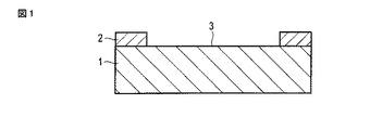
図1に示すように、セラミックス基板1上に第一のマスキング2を施す。第一のマスキング2は、銅回路パターン及びろう材はみ出し部になる領域3以外の部分に形成される。第一のマスキング2を行わない場合、銅回路間隔に必要以上にはみ出したろう材による導通の恐れがあるため、ろう材はみ出し部を、ろう材除去用のフッ酸やアルカリ液でエッチングする必要がある。このエッチングによりろう材はみ出し部に空隙が発生するため、銅回路板端部の応力集中緩和となる熱応力の均一分散が起こらなくなり、セラミック基板のクラック発生などが生じ易くなってしまうことを本発明者らは究明したのである。第一のマスキング工程を行うことにより、ろう材はみ出し部のエッチングが不要になるため、ろう材はみ出し部の気孔を少なくすることができ、大きな気孔の形成を防止できる。
As shown in FIG. 1, a
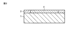
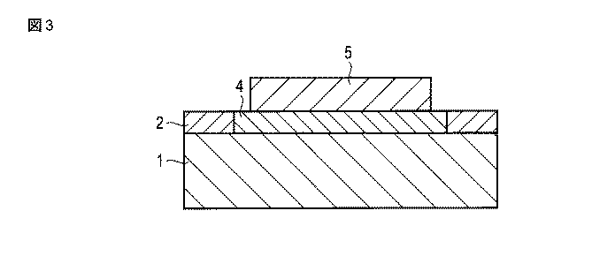
次いで、図2に示すように、第一のマスキングが施されていない領域3に、Ag、Cu及びTiを含むろう材4を印刷又は塗布する。印刷又は塗布されるろう材層4の面積は、銅回路板形状よりもはみ出す長さ分だけ大きくする。なお、はみ出させる方法は、予め銅回路板形状よりもはみ出す長さ分だけ大きくろう材を印刷・塗布する方法に限定されず、例えば、銅回路板形状と同形状に印刷・塗布したろう材を接合によりはみ出させる方法を採用することが可能である。また、ろう材層の厚さは10〜40μmが好ましい。10μm未満では十分な接合強度が得られないおそれがあり、40μmを超えるとこれ以上の効果が得られずコストアップの要因となる。
Next, as shown in FIG. 2, a brazing material 4 containing Ag, Cu and Ti is printed or applied to the
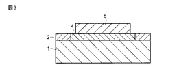
図3に示すように、ろう材層4上に銅板5を載せ、加熱によりセラミックス基板と銅板を接合する(活性金属接合法)。活性金属接合の条件は、真空中や窒素雰囲気のような不活性雰囲気中にて温度700〜900℃で10〜120分間の加熱であることが望ましい。この活性金属接合により、ろう材層4中にTi相およびTiN相が生成する。生成量は、例えば、使用するろう材の組成、活性金属接合の条件等により調整可能である。また、セラミックス基板が窒化物セラミックス基板(AlN、Si3N4など)の場合、TiN相はろう材中のTiと窒化物セラミックス基板の窒素が反応してできるので、この点も考慮して調整する。
As shown in FIG. 3, a
セラミックス基板1と銅板5には、位置合わせ用のマーキングが施されていることが望ましい。例えば、セラミックス基板1に位置合わせ用の穴もしくは溝を形成し、一方、銅板5にこの穴や溝と対応する突起を設けることができる。
The
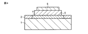
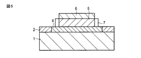
次いで、図4に示すように、銅回路パターンとなる領域の銅板5上に第二のマスキング6を施す。その後、図5に示すように、銅板5における第二のマスキング6がなされていない箇所7をエッチングにより除去し、銅回路パターンを形成する。エッチング液は、銅板エッチング用のエッチング液を使用することができ、具体例は、塩化第二鉄、塩化第二銅等が挙げられる。銅板エッチング用のエッチング液を使用しているため、ろう材はみ出し部が必要以上にエッチング液にさらされると、ろう材中のCuがエッチングされてしまう。この現象が気孔の原因となる。
Next, as shown in FIG. 4,
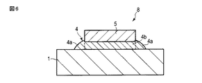
引き続き、第一、第二のマスキング2,6を除去することにより、図6に示すような第1の実施形態のセラミックス回路基板8が得られる。なお、第一、第二のマスキングは、印刷可能な有機インクレジスト等から形成することができる。
Subsequently, the ceramic circuit board 8 of the first embodiment as shown in FIG. 6 is obtained by removing the first and
上記エッチングの際、銅回路パターン5の側面から外側にはみ出しているろう材層(ろう材はみ出し部)4a中のCu成分の一部が一緒に除去されるため、ろう材はみ出し部4a中のTi相およびTiN相の合計量のろう材はみ出し部4a全体に対する比率が増加する。一方、銅回路パターン5とセラミックス基板1の間に介在されているろう材層(接合層)4bの組成は、エッチングによる影響を受けない。その結果、ろう材はみ出し部4a中のTi相およびTiN相の合計は、3質量%以上に増加し、かつ接合層4b中のTi相およびTiN相の合計量と異なるものになる。また、銅回路パターン形成のためのエッチングであるため、ろう材はみ出し部4を必要以上にエッチング液にさらさないで済むことから、ろう材はみ出し部4aに空隙が発生せず、ろう材はみ出し部4a中の1個当たりの面積が200μm2以下の空隙が1つ以下(0を含む)になる。なお、200μm2を超える空隙が存在しないことは言うまでもない。
At the time of the etching, a part of the Cu component in the brazing filler metal layer (brazing filler metal protruding portion) 4a protruding outward from the side surface of the
ろう材はみ出し部4a中のTi相およびTiN相の合計量は、ろう材はみ出し部の長さ、エッチング条件等により調整可能である。また、1個当たりの面積が200μm2以下の空隙数は、エッチング条件等により調整可能である。例えば、エッチング液中の塩化第二鉄や塩化第二銅の濃度を15wt%以下と少なめにすることなどが挙げられる。なお、エッチング液中の塩化第二鉄や塩化第二銅の濃度の下限は特に限定されるものではないが、あまり少ないとエッチングの進行が遅くなり製造時間が長くなるので5wt%以上が好ましい。また、ろう材はみ出し部4aの形状は図6に示した断面R形状に限られるものではなく、断面長方形形状であってもよい。
The total amount of the Ti phase and the TiN phase in the brazing
また、エッチング処理後の銅回路パターン5の端面は断面R形状、斜面形状(銅回路パターン5の上面からろう材層4側に向かう下り斜面、例えば、富士山の裾野のような裾野形状)であることが好ましい。このような形状であれば、銅回路板の端面の応力を緩和し易い。
Moreover, the end surface of the
以下、実施例で更に具体的に本発明の実施形態を説明する。 Hereinafter, embodiments of the present invention will be described in more detail with reference to examples.
(試料1〜9)
各試料を以下に説明する方法で製造した。まず、50×60mmのセラミックス基板の銅回路パターン形成面に第一のマスキングを行った。第一のマスキングは、銅回路パターンとろう材はみ出し部となる所定のサイズの領域を除いて行った。次に、第一のマスキングを形成していない領域にAg−Cu−Ti系ろう材(Ag67重量%−Cu20重量%−Sn10重量%−Ti3重量%)を厚さ15μmで印刷、また裏面にも厚さ15μmで印刷し、セラミックス基板の両面に銅板を配置し、真空中10−3Pa、800℃で40分間の加熱によりセラミック基板と接合した。銅回路板は、20×20mmの銅板を1mm間隔で2枚配置した。
(Samples 1-9)
Each sample was manufactured by the method demonstrated below. First, the first masking was performed on the copper circuit pattern forming surface of the 50 × 60 mm ceramic substrate. The first masking was performed except for a region of a predetermined size that would be a copper circuit pattern and a brazing material protrusion. Next, an Ag—Cu—Ti brazing material (Ag 67 wt% —Cu 20 wt% —Sn 10 wt% —
次に、銅板上にパターン形状の第二のマスキング(エッチングレジスト)を印刷し、塩化第二鉄液(塩化第二鉄の濃度5〜15wt%)によってエッチング処理を行って回路パターンを形成した後、レジストを剥離して回路基板を得た。なお、試料1,2で用いるAlN基板および試料3,4のAl2O3基板の厚さは0.635mm、試料5〜9で用いるSi3N4基板の厚さは0.32mmとした。また、AlN基板は熱伝導率170W/m・Kかつ3点曲げ強度450MPa、Al2O3基板は熱伝導率25W/m・Kかつ3点曲げ強度450MPa、Si3N4基板は熱伝導率90W/m・Kかつ3点曲げ強度700MPaのものを用いた。
Next, after a pattern-shaped second masking (etching resist) is printed on the copper plate and a circuit pattern is formed by performing an etching process with a ferric chloride solution (ferric chloride concentration of 5 to 15 wt%) The resist was removed to obtain a circuit board. The thicknesses of the AlN substrate used in
銅回路板厚さ、セラミックス基板材種、銅回路板の側面から外側へのはみ出し量(mm単位及び銅回路間隔を100%とした際の割合)、接合層中におけるTi相およびTiN相の合計量、はみ出しろう材中におけるTi相およびTiN相の合計量、はみ出しろう材中の1個当たりの面積200μm2以下の空隙数を下記表1に示す。 Copper circuit board thickness, ceramic substrate material type, protrusion amount from side to outside of copper circuit board (ratio when mm unit and copper circuit interval is 100%), total of Ti phase and TiN phase in bonding layer Table 1 below shows the amount, the total amount of the Ti phase and the TiN phase in the protruding brazing material, and the number of voids having an area of 200 μm 2 or less per piece in the protruding brazing material.
また、得られたセラミックス回路基板について、目視及び超音波探傷による接合不良とろう接欠陥を検査し、−50℃、30分→室温、10分→155℃、30分→室温、10分を1サイクルとして熱サイクル試験を実施した。試験後の回路基板については、目視や超音波探傷により、回路板の剥離やセラミックス基板のクラック発生等、異常の有無を検査した。検査した後の結果を下記表1に示す。
AlN基板を用いた試料1と試料2の結果から、はみ出しろう材中のTi相およびTiN相の合計が3質量%以上かつ接合層中のTi相およびTiN相の合計量と異なり、はみ出しろう材中の1個当たりの面積が200μm2以下の空隙が1つ以下である試料1,2は、耐熱サイクルに優れていることがわかる。
From the results of
Al2O3基板を用いた試料3と試料4の結果から、はみ出しろう材中のTi相およびTiN相の合計が3質量%以上かつ接合層中のTi相およびTiN相の合計量と異なり、はみ出しろう材中の1個当たりの面積が200μm2以下の空隙が1つ以下である試料3,4は、耐熱サイクルに優れていることがわかる。
From the results of
Si3N4基板を用いた試料5〜9の結果から、はみ出しろう材中のTi相およびTiN相の合計が3質量%以上かつ接合層中のTi相およびTiN相の合計量と異なり、はみ出しろう材中の1個当たりの面積が200μm2以下の空隙が1つ以下である試料5〜9は、耐熱サイクルに優れていることがわかる。なお、試料1〜9は面積200μm2を超える空隙は存在しなかった。また、試料1〜9は銅回路板の端面は傾斜形状(裾野形状)となっていた。
From the results of
(比較例1)
セラミックス基板(AlN基板)の全面に試料1〜9で用いるのと同様な組成のAg−Cu−Ti系ろう材を厚さ15μmで塗布し、その上に銅板を接合し、加熱接合した。その後、塩化第二鉄で銅板をパターン形状にエッチングし、さらにフッ酸を用いてはみ出しろう材をエッチングした。はみ出し量は試料2と同様に0.12mmとした。はみ出しろう材中の1個当たりの面積200μm2以下の空隙数をカウントしたところ、8個であった。また、試料1〜9と同様の熱サイクル試験を行ったところ、340回となった。
(Comparative Example 1)
An Ag—Cu—Ti brazing material having the same composition as that used in
(試料11〜15)
Ag63重量%、Cu32重量%及びTi5重量%を含む活性金属ろう材組成を用いて、銅板と窒化珪素基板(板厚0.32mm)を接合したセラミックス回路基板を製造した。マスキング及び活性金属接合は、試料1〜9で説明したのと同様な条件で行った。
(Samples 11-15)
Using an active metal brazing material composition containing 63 wt% Ag, 32 wt% Cu and 5 wt% Ti, a ceramic circuit board in which a copper plate and a silicon nitride substrate (plate thickness 0.32 mm) were joined was manufactured. Masking and active metal bonding were performed under the same conditions as described for Samples 1-9.
銅回路板厚さ、セラミックス基板材種、銅回路板の側面から外側へのはみ出し量(mm単位及び銅回路間隔を100%とした際の割合)、接合層中におけるTi相およびTiN相の合計量、はみ出しろう材中におけるTi相およびTiN相の合計量、はみ出しろう材中の1個当たりの面積200μm2以下の空隙数を下記表2に示す。 Copper circuit board thickness, ceramic substrate material type, protrusion amount from side to outside of copper circuit board (ratio when mm unit and copper circuit interval is 100%), total of Ti phase and TiN phase in bonding layer Table 2 below shows the amount, the total amount of Ti phase and TiN phase in the brazing filler metal, and the number of voids having an area of 200 μm 2 or less per piece in the brazing filler metal.
また、試料1〜9で説明したのと同様な条件の熱サイクル試験を実施して測定した耐熱サイクル数を下記表2に示す。
表2の結果から、活性金属ろう材の組成を変更した場合にも、はみ出しろう材中のTi相およびTiN相の合計が3質量%以上かつ接合層中のTi相およびTiN相の合計量と異なり、はみ出しろう材における1個当たりの面積が200μm2以下の空隙が1つ以下である試料11〜15は、耐熱サイクル特性に優れていることがわかる。また、セラミックス基板として窒化珪素を用いた場合は3000回の熱サイクル後も、接合欠陥がなく、セラミック基板と銅回路板端部の間にクラックが認められず、耐熱衝撃性にも優れていた。なお、試料11〜15は面積200μm2を超える空隙は存在しなかった。また、試料11〜15は銅回路板の端面は傾斜形状(裾野形状)となっていた。 From the results in Table 2, even when the composition of the active metal brazing material is changed, the total amount of Ti phase and TiN phase in the brazing filler metal is 3% by mass or more, and the total amount of Ti phase and TiN phase in the bonding layer In contrast, it can be seen that Samples 11 to 15 in which the area per piece in the protruding brazing material has one or less voids of 200 μm 2 or less are excellent in heat resistance cycle characteristics. In addition, when silicon nitride was used as the ceramic substrate, there were no bonding defects even after 3000 thermal cycles, no cracks were observed between the ceramic substrate and the end of the copper circuit board, and the thermal shock resistance was excellent. . In Samples 11 to 15, there was no void having an area exceeding 200 μm 2 . In Samples 11 to 15, the end face of the copper circuit board had an inclined shape (skirt shape).
(試料16〜19)
40×60×0.32mmの窒化珪素(Si3N4)基板の銅回路パターン形成面に第一のマスキングを行った。第一のマスキングは、銅回路パターンとろう材はみ出し部となる所定のサイズの領域を除いて行った。次に、第一のマスキングを形成していない領域にAg−Cu−Ti系ろう材を印刷、また裏面にも印刷し、窒化珪素基板の両面に銅板を配置し、真空中10−3Pa、760〜810℃で20〜50分間の加熱により窒化珪素基板と接合した。銅回路板は、15×20×0.3mmの銅板を1mm間隔で2枚配置した。なお、Ag−Cu−Tiろう材の組成およびろう材層厚さは表3の通りとした。なお、窒化珪素(Si3N4)基板は熱伝導率85W/m・Kかつ3点曲げ強度750MPaのものを用いた。
(Samples 16 to 19)
First masking was performed on the copper circuit pattern forming surface of a 40 × 60 × 0.32 mm silicon nitride (Si 3 N 4 ) substrate. The first masking was performed except for a region of a predetermined size that would be a copper circuit pattern and a brazing material protrusion. Next, an Ag-Cu-Ti-based brazing material is printed in a region where the first masking is not formed, and also printed on the back surface, a copper plate is disposed on both sides of the silicon nitride substrate, and 10-3 Pa in vacuum, The silicon nitride substrate was bonded by heating at 760 to 810 ° C. for 20 to 50 minutes. As the copper circuit board, two 15 × 20 × 0.3 mm copper plates were arranged at intervals of 1 mm. The composition of the Ag—Cu—Ti brazing material and the thickness of the brazing material layer were as shown in Table 3. A silicon nitride (Si 3 N 4 ) substrate having a thermal conductivity of 85 W / m · K and a three-point bending strength of 750 MPa was used.
次に、銅板上にパターン形状の第二のマスキング(エッチングレジスト)を印刷し、塩化第二銅液(塩化第二銅の濃度5〜15wt%)によってエッチング処理を行って回路パターンを形成した後、レジストを剥離して回路基板を得た。 Next, after a pattern-shaped second masking (etching resist) is printed on the copper plate and a circuit pattern is formed by performing an etching process with a cupric chloride solution (cupric chloride concentration of 5 to 15 wt%). The resist was removed to obtain a circuit board.
得られた窒化珪素回路基板に対し、試料1と同様の測定を行った。その結果を表4に示す。
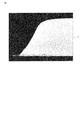
表3、表4から分かる通り、ろう材組成やろう材層厚さを変えても優れた特性を示すことが確認された。また、窒化珪素基板を用いているので5000回の熱サイクル後も、接合欠陥がなく、窒化珪素基板と銅回路板端部の間にクラックが認められず、耐熱衝撃性にも優れていた。なお、試料16〜19は面積200μm2を超える空隙は存在しなかった。また、試料17は、図7の銅回路板5の厚さ方向の断面の光学顕微鏡写真に示す通り、銅回路板5の端面は傾斜形状(裾野形状)となっていた。また、他の試料に関しても同様の形状となっていた。
As can be seen from Tables 3 and 4, it was confirmed that excellent characteristics were exhibited even when the brazing filler metal composition and the brazing filler metal layer thickness were changed. Further, since a silicon nitride substrate was used, there were no bonding defects even after 5000 thermal cycles, no cracks were observed between the silicon nitride substrate and the end of the copper circuit board, and the thermal shock resistance was excellent. In Samples 16 to 19, there was no void having an area exceeding 200 μm 2 . In addition, as shown in the optical micrograph of the cross section in the thickness direction of the
以上説明した通りに、本発明の実施形態及び実施例によると、信頼性の高いセラミックス回路基板ができることから産業上極めて有効である。 As described above, according to the embodiments and examples of the present invention, a highly reliable ceramic circuit board can be obtained, which is extremely effective in the industry.
1…セラミックス基板、2…第一のマスキング、3…銅回路パターン及びろう材はみ出し部になる領域、4…ろう材層、5…銅板、6…第二のマスキング、8…セラミックス回路基板。
DESCRIPTION OF
本発明の実施形態は、セラミックス回路基板の製造方法に関する。 Embodiments of the present invention, related to method of manufacturing a ceramic circuit board.
本発明の実施形態は、このような技術的課題に鑑みてなされたもので、空隙等による欠陥の少ないろう材はみ出し部を有し、耐熱サイクルが向上されたセラミックス回路基板の製造方法を提供することを目的とする。 Embodiments of the present invention has been made in view of such technical problems, has fewer brazing material protruded portion defect caused by voids, etc., to provide a method of manufacturing a ceramic circuit board which heat cycle is improved For the purpose.
本発明の実施形態によれば、セラミックス基板の少なくとも一方の面に、Ag、Cu及びTiを含むろう材層を介して銅回路パターンとしての銅回路板を接合する工程、および前記銅回路板の側面から外側にはみ出した前記ろう材層で形成されたろう材はみ出し部を形成する工程を含むセラミックス回路基板の製造方法である。前記ろう材層は、前記セラミックス基板と前記銅回路板との間に介在した接合層部から外側にはみ出した、長さが0.01mm以上で、かつ銅回路板の間隔の30%以下であるろう材はみ出し部を有し、前記ろう材層は、Ag:90〜50重量%、Snおよび/またはInからなる元素:5〜15重量%、Ti:0.1〜6重量%、残部Cuおよび不可避不純物からなる組成を有する。前記ろう材はみ出し部中のTi相およびTiN相の合計割合は、3質量%以上40質量%以下で、かつ前記ろう材層の接合層部中のTi相およびTiN相の合計割合よりも多く、前記ろう材はみ出し部において、1個当たりの面積が200μm 2 を超える空隙が存在せず、かつ1個当たりの面積が200μm2以下の空隙が1つ以下(0を含む)である。 According to an embodiment of the present invention, on at least one surface of the ceramic substrate, Ag, step bonding the copper circuit board as copper circuit pattern via a brazing material layer containing Cu and Ti, and the copper circuit board Ru manufacturing method der ceramic circuit board including a step of forming a brazing material protruding portion formed in the brazing material layer protruding outwardly from the side. The brazing material layer protrudes outward from the bonding layer portion interposed between the ceramic substrate and the copper circuit board, and has a length of 0.01 mm or more and 30% or less of the interval between the copper circuit boards. The brazing material layer has a protruding portion, and the brazing material layer is composed of Ag: 90 to 50% by weight, element consisting of Sn and / or In: 5 to 15% by weight, Ti: 0.1 to 6% by weight, balance Cu and It has a composition consisting of inevitable impurities. The total proportion of the Ti phase and the TiN phase in the brazing material protruding portion is 3% by mass or more and 40% by mass or less, and more than the total proportion of the Ti phase and the TiN phase in the bonding layer portion of the brazing material layer, In the protruding portion of the brazing material, there are no voids having an area of more than 200 μm 2 per piece , and one or less (including 0) voids having an area of 200 μm 2 or less per piece.
本発明の実施形態によれば、空隙等による欠陥の少ないろう材はみ出し部を有し、耐熱サイクルが向上されたセラミックス回路基板の製造方法を提供することができる。 According to an embodiment of the present invention, it has fewer brazing material protruded portion defect caused by voids and the like, it is possible to provide a method of manufacturing a ceramic circuit board which heat cycle is improved.
以上説明した通り、本発明の実施形態及び実施例によると、信頼性の高いセラミックス回路基板ができることから産業上極めて有効である。
以下に、本願出願の当初の特許請求の範囲に記載された発明を付記する。
[1] セラミックス基板と、
前記セラミックス基板の少なくとも一方の面に、Ag、Cu及びTiを含むろう材層を介して接合された銅回路板と、
前記銅回路板の側面から外側にはみ出した前記ろう材層で形成されたろう材はみ出し部とを備えるセラミックス回路基板であって、
前記ろう材はみ出し部中のTi相およびTiN相の合計は3質量%以上で、かつ前記セラミックス基板と前記銅回路板の間に介在された前記ろう材層中のTi相およびTiN相の合計量と異なり、前記ろう材はみ出し部における1個当たりの面積が200μm 2 以下の空隙が1つ以下(0を含む)であることを特徴とするセラミックス回路基板。
[2] 前記ろう材はみ出し部中のTi相およびTiN相の合計は3質量%以上40質量%以下であることを特徴とする上記[1]記載のセラミックス回路基板。
[3] 前記ろう材はみ出し部のはみ出し長さが0.01mm以上で、かつ前記銅回路板の間隔の30%以下であることを特徴とする上記[1]または[2]のいずれか1項に記載のセラミックス回路基板。
[4] 前記セラミックス基板が窒化珪素、窒化アルミニウムあるいはアルミナからなり、前記銅回路板の厚さが0.25mm以上であることを特徴とする上記[1]ないし上記[3]のいずれか1項に記載のセラミックス回路基板。
[5] 前記ろう材層は、Ag:90〜50重量%、Snおよび/またはInからなる元素:5〜15重量%、Ti:0.1〜6重量%、残部Cuおよび不可避不純物からなる組成のろう材を用いて形成されることを特徴とする請求項1ないし請求項4のいずれか1項に記載のセラミックス回路基板。
[6] セラミックス基板上における、銅回路パターン及びろう材はみ出し部となる領域以外の部分に第一のマスキングを施す工程と、
前記第一のマスキングが施されていない領域に、Ag、Cu及びTiを含むろう材層を形成する工程と、
前記ろう材層上に銅板を載せ、加熱により前記セラミックス基板と前記銅板を接合する工程と、
前記銅板上の銅回路パターンとなる領域に第二のマスキングを施す工程と、
エッチングにより銅回路パターンを形成する工程と
を備えることを特徴とするセラミックス回路基板の製造方法。
[7] 前記エッチングに用いるエッチング液が塩化第二鉄または塩化第二銅であることを特徴とする上記[6]記載のセラミックス回路基板の製造方法。
[8] 前記セラミックス基板と前記銅板に位置合わせ用マーキングが施されていることを特徴とする上記[6]または[7]のいずれか1項に記載のセラミックス基板の製造方法。
[9] 前記第一のマスキング及び前記第二のマスキングの材料が印刷可能な有機インクレジストであることを特徴とする上記[6]ないし上記[8]のいずれか1項に記載のセラミックス回路基板の製造方法。
Above-described passing is, according to the embodiments and examples of the present invention is extremely effective industrially because it can reliable ceramic circuit board.
Hereinafter, the invention described in the scope of claims of the present application will be appended.
[1] a ceramic substrate;
A copper circuit board joined to at least one surface of the ceramic substrate via a brazing filler metal layer containing Ag, Cu and Ti;
A ceramic circuit board comprising a brazing material protruding portion formed of the brazing material layer protruding outward from the side surface of the copper circuit board;
The total amount of Ti phase and TiN phase in the brazing material protruding portion is 3% by mass or more, and is different from the total amount of Ti phase and TiN phase in the brazing material layer interposed between the ceramic substrate and the copper circuit board. A ceramic circuit board having one or less (including 0) voids each having an area of 200 μm 2 or less in the protruding portion of the brazing material .
[2] The ceramic circuit board according to [1], wherein a total of the Ti phase and the TiN phase in the protruding portion of the brazing material is 3% by mass or more and 40% by mass or less.
[3] Either one of the above [1] or [2], wherein the protruding length of the protruding portion of the brazing material is 0.01 mm or more and 30% or less of the interval between the copper circuit boards. The ceramic circuit board according to 1.
[4] Any one of [1] to [3], wherein the ceramic substrate is made of silicon nitride, aluminum nitride, or alumina, and the thickness of the copper circuit board is 0.25 mm or more. The ceramic circuit board according to 1.
[5] The brazing filler metal layer is composed of Ag: 90 to 50% by weight, element consisting of Sn and / or In: 5 to 15% by weight, Ti: 0.1 to 6% by weight, balance Cu and inevitable impurities. The ceramic circuit board according to
[6] A step of performing a first masking on a portion of the ceramic substrate other than a region serving as a copper circuit pattern and a brazing material protruding portion;
Forming a brazing filler metal layer containing Ag, Cu and Ti in a region not subjected to the first masking;
Placing a copper plate on the brazing material layer, and joining the ceramic substrate and the copper plate by heating;
Applying a second mask to the copper circuit pattern on the copper plate;
Forming a copper circuit pattern by etching; and
A method for producing a ceramic circuit board, comprising:
[7] The method for producing a ceramic circuit board according to [6], wherein the etching solution used for the etching is ferric chloride or cupric chloride.
[8] The method for producing a ceramic substrate according to any one of [6] or [7], wherein the ceramic substrate and the copper plate are provided with alignment markings.
[9] The ceramic circuit board according to any one of [6] to [8], wherein the first masking material and the second masking material are printable organic ink resists. Manufacturing method.
Claims (9)
前記セラミックス基板の少なくとも一方の面に、Ag、Cu及びTiを含むろう材層を介して接合された銅回路板と、
前記銅回路板の側面から外側にはみ出した前記ろう材層で形成されたろう材はみ出し部とを備えるセラミックス回路基板であって、
前記ろう材はみ出し部中のTi相およびTiN相の合計は3質量%以上で、かつ前記セラミックス基板と前記銅回路板の間に介在された前記ろう材層中のTi相およびTiN相の合計量と異なり、前記ろう材はみ出し部における1個当たりの面積が200μm2以下の空隙が1つ以下(0を含む)であることを特徴とするセラミックス回路基板。 A ceramic substrate;
A copper circuit board joined to at least one surface of the ceramic substrate via a brazing filler metal layer containing Ag, Cu and Ti;
A ceramic circuit board comprising a brazing material protruding portion formed of the brazing material layer protruding outward from the side surface of the copper circuit board;
The total amount of Ti phase and TiN phase in the brazing material protruding portion is 3% by mass or more, and is different from the total amount of Ti phase and TiN phase in the brazing material layer interposed between the ceramic substrate and the copper circuit board. A ceramic circuit board having one or less (including 0) voids each having an area of 200 μm 2 or less in the protruding portion of the brazing material.
前記第一のマスキングが施されていない領域に、Ag、Cu及びTiを含むろう材層を形成する工程と、
前記ろう材層上に銅板を載せ、加熱により前記セラミックス基板と前記銅板を接合する工程と、
前記銅板上の銅回路パターンとなる領域に第二のマスキングを施す工程と、
エッチングにより銅回路パターンを形成する工程と
を備えることを特徴とするセラミックス回路基板の製造方法。 A step of applying a first masking to a portion other than a region to be a copper circuit pattern and a brazing material protrusion on the ceramic substrate;
Forming a brazing filler metal layer containing Ag, Cu and Ti in a region not subjected to the first masking;
Placing a copper plate on the brazing material layer, and joining the ceramic substrate and the copper plate by heating;
Applying a second mask to the copper circuit pattern on the copper plate;
And a step of forming a copper circuit pattern by etching.
Applications Claiming Priority (2)
| Application Number | Priority Date | Filing Date | Title |
|---|---|---|---|
| JP2009213511 | 2009-09-15 | ||
| JP2009213511 | 2009-09-15 |
Related Parent Applications (1)
| Application Number | Title | Priority Date | Filing Date |
|---|---|---|---|
| JP2016075911A Division JP6271629B2 (en) | 2009-09-15 | 2016-04-05 | Ceramic circuit boards for power modules |
Publications (2)
| Publication Number | Publication Date |
|---|---|
| JP2017191943A true JP2017191943A (en) | 2017-10-19 |
| JP6334781B2 JP6334781B2 (en) | 2018-05-30 |
Family
ID=43758676
Family Applications (7)
| Application Number | Title | Priority Date | Filing Date |
|---|---|---|---|
| JP2011531941A Active JP5637992B2 (en) | 2009-09-15 | 2010-09-15 | Manufacturing method of ceramic circuit board |
| JP2014148865A Active JP6158144B2 (en) | 2009-09-15 | 2014-07-22 | Ceramic circuit board |
| JP2016075911A Active JP6271629B2 (en) | 2009-09-15 | 2016-04-05 | Ceramic circuit boards for power modules |
| JP2016075910A Active JP6271628B2 (en) | 2009-09-15 | 2016-04-05 | Power module |
| JP2017101088A Active JP6400788B2 (en) | 2009-09-15 | 2017-05-22 | Power module manufacturing method |
| JP2017101087A Active JP6400787B2 (en) | 2009-09-15 | 2017-05-22 | Manufacturing method of ceramic circuit board for power module |
| JP2017101086A Active JP6334781B2 (en) | 2009-09-15 | 2017-05-22 | Manufacturing method of ceramic circuit board |
Family Applications Before (6)
| Application Number | Title | Priority Date | Filing Date |
|---|---|---|---|
| JP2011531941A Active JP5637992B2 (en) | 2009-09-15 | 2010-09-15 | Manufacturing method of ceramic circuit board |
| JP2014148865A Active JP6158144B2 (en) | 2009-09-15 | 2014-07-22 | Ceramic circuit board |
| JP2016075911A Active JP6271629B2 (en) | 2009-09-15 | 2016-04-05 | Ceramic circuit boards for power modules |
| JP2016075910A Active JP6271628B2 (en) | 2009-09-15 | 2016-04-05 | Power module |
| JP2017101088A Active JP6400788B2 (en) | 2009-09-15 | 2017-05-22 | Power module manufacturing method |
| JP2017101087A Active JP6400787B2 (en) | 2009-09-15 | 2017-05-22 | Manufacturing method of ceramic circuit board for power module |
Country Status (6)
| Country | Link |
|---|---|
| US (2) | US8785785B2 (en) |
| EP (2) | EP3273755B1 (en) |
| JP (7) | JP5637992B2 (en) |
| HU (2) | HUE041380T2 (en) |
| PL (1) | PL2480052T3 (en) |
| WO (1) | WO2011034075A1 (en) |
Families Citing this family (28)
| Publication number | Priority date | Publication date | Assignee | Title |
|---|---|---|---|---|
| WO2011034075A1 (en) * | 2009-09-15 | 2011-03-24 | 株式会社 東芝 | Ceramic circuit board and process for producing same |
| JP5976678B2 (en) | 2011-12-20 | 2016-08-24 | 株式会社東芝 | Ceramic copper circuit board |
| US20160152004A1 (en) * | 2013-04-26 | 2016-06-02 | Kyocera Corporation | Composite laminate and electronic device |
| CN105452194B (en) | 2013-08-08 | 2017-05-03 | 株式会社东芝 | Circuit substrate and semiconductor device |
| EP3125286B1 (en) * | 2014-03-26 | 2019-05-08 | Kyocera Corporation | Circuit board and electronic device provided with same |
| US9731384B2 (en) * | 2014-11-18 | 2017-08-15 | Baker Hughes Incorporated | Methods and compositions for brazing |
| DE102015110607A1 (en) * | 2015-07-01 | 2017-01-05 | Epcos Ag | Method for producing an electrical component |
| JP6829204B2 (en) * | 2015-09-28 | 2021-02-10 | 株式会社東芝 | Silicon nitride circuit board and semiconductor module using it |
| CN110690187B (en) * | 2015-09-28 | 2023-12-12 | 株式会社东芝 | Circuit board and semiconductor device |
| EP3598485B1 (en) | 2015-12-28 | 2020-10-07 | NGK Insulators, Ltd. | Bonded substrate and method for manufacturing bonded substrate |
| EP3471517A4 (en) * | 2016-06-10 | 2019-06-05 | Tanaka Kikinzoku Kogyo K.K. | Ceramic circuit board and method for manufacturing ceramic circuit board |
| EP3486942A4 (en) | 2016-07-14 | 2020-03-18 | Kabushiki Kaisha Toshiba, Inc. | Ceramic circuit board and semiconductor module |
| JP7013374B2 (en) * | 2016-07-28 | 2022-01-31 | 株式会社東芝 | Bonds, circuit boards, and semiconductor devices |
| CN109478538B (en) | 2016-07-28 | 2022-04-01 | 株式会社东芝 | Circuit board and semiconductor module |
| US11043465B2 (en) * | 2017-05-11 | 2021-06-22 | Sumitomo Electric Industries, Ltd. | Semiconductor device |
| WO2019006101A1 (en) * | 2017-06-30 | 2019-01-03 | Kyocera International, Inc. | Microelectronic package construction enabled through ceramic insulator strengthening and design |
| CN107369741A (en) * | 2017-07-13 | 2017-11-21 | 东莞市凯昶德电子科技股份有限公司 | LED support module with integrated metal box dam and preparation method thereof |
| KR102521140B1 (en) * | 2017-07-25 | 2023-04-12 | 덴카 주식회사 | Ceramic circuit board and its manufacturing method |
| US10695875B2 (en) * | 2018-03-19 | 2020-06-30 | Asia Vital Components Co., Ltd. | Soldering method of soldering jig |
| JPWO2019225273A1 (en) | 2018-05-23 | 2021-05-27 | 住友ベークライト株式会社 | Circuit board manufacturing method |
| JP7243182B2 (en) * | 2018-12-26 | 2023-03-22 | 三菱マテリアル株式会社 | Insulated circuit board manufacturing method and its insulated circuit board |
| JP7289910B2 (en) * | 2019-03-14 | 2023-06-12 | 日本碍子株式会社 | BONDED SUBSTRATE AND BONDED SUBSTRATE MANUFACTURING METHOD |
| WO2020208698A1 (en) | 2019-04-09 | 2020-10-15 | 日本碍子株式会社 | Bonded substrate and method for manufacturing bonded substrate |
| EP4026819A4 (en) | 2019-09-02 | 2023-12-06 | Kabushiki Kaisha Toshiba | Joined body, circuit board, and semiconductor device |
| CN113053833A (en) * | 2019-12-26 | 2021-06-29 | 财团法人工业技术研究院 | Semiconductor device and manufacturing method thereof |
| JPWO2021200810A1 (en) * | 2020-03-30 | 2021-10-07 | ||
| DE102020111700A1 (en) | 2020-04-29 | 2021-11-04 | Rogers Germany Gmbh | Carrier substrate and method for producing a carrier substrate |
| WO2023074470A1 (en) | 2021-10-25 | 2023-05-04 | 株式会社 東芝 | Ceramic copper circuit board and semiconductor device using same |
Citations (4)
| Publication number | Priority date | Publication date | Assignee | Title |
|---|---|---|---|---|
| JPH10326949A (en) * | 1997-05-26 | 1998-12-08 | Denki Kagaku Kogyo Kk | Circuit board |
| JP2007173577A (en) * | 2005-12-22 | 2007-07-05 | Hitachi Metals Ltd | Ceramic circuit board |
| JP2007281219A (en) * | 2006-04-07 | 2007-10-25 | Hitachi Metals Ltd | Ceramic circuit board and its manufacturing method |
| WO2008004552A1 (en) * | 2006-07-04 | 2008-01-10 | Kabushiki Kaisha Toshiba | Ceramic-metal bonded body, method for manufacturing the bonded body and semiconductor device using the bonded body |
Family Cites Families (23)
| Publication number | Priority date | Publication date | Assignee | Title |
|---|---|---|---|---|
| FR1393352A (en) * | 1963-01-21 | 1965-03-26 | Ibm | Manufacture of micro-circuits |
| US5541368A (en) * | 1994-07-15 | 1996-07-30 | Dell Usa, L.P. | Laminated multi chip module interconnect apparatus |
| JPH10190176A (en) * | 1996-12-26 | 1998-07-21 | Denki Kagaku Kogyo Kk | Circuit board |
| US6286206B1 (en) * | 1997-02-25 | 2001-09-11 | Chou H. Li | Heat-resistant electronic systems and circuit boards |
| TW453137B (en) * | 1997-08-25 | 2001-09-01 | Showa Denko Kk | Electrode structure of silicon semiconductor device and the manufacturing method of silicon device using it |
| JP3447532B2 (en) * | 1997-09-19 | 2003-09-16 | 科学技術振興事業団 | Brazing structure and metallized structure |
| JP3847954B2 (en) | 1998-05-22 | 2006-11-22 | 株式会社東芝 | Manufacturing method of ceramic circuit board |
| US6700053B2 (en) * | 2000-07-03 | 2004-03-02 | Komatsu Ltd. | Thermoelectric module |
| DE10165080B4 (en) * | 2000-09-20 | 2015-05-13 | Hitachi Metals, Ltd. | Silicon nitride powder and sintered body and method of making the same and printed circuit board therewith |
| JP5038565B2 (en) * | 2000-09-22 | 2012-10-03 | 株式会社東芝 | Ceramic circuit board and manufacturing method thereof |
| CN1226752C (en) * | 2001-01-29 | 2005-11-09 | 捷时雅株式会社 | Composite particle for dielectrics, ultramicro particulate composite resin particle, composition for forming dielectrics and use thereof |
| JP4887583B2 (en) * | 2001-08-09 | 2012-02-29 | Dowaメタルテック株式会社 | Manufacturing method of ceramic circuit board |
| JP3648189B2 (en) * | 2001-09-28 | 2005-05-18 | 同和鉱業株式会社 | Metal-ceramic circuit board |
| JP4362597B2 (en) * | 2003-05-30 | 2009-11-11 | Dowaメタルテック株式会社 | Metal-ceramic circuit board and manufacturing method thereof |
| JP3816508B2 (en) * | 2004-11-04 | 2006-08-30 | 三井金属鉱業株式会社 | Capacitor layer forming material and printed wiring board with built-in capacitor layer obtained using the capacitor layer forming material |
| JP4345066B2 (en) * | 2005-05-24 | 2009-10-14 | 日立金属株式会社 | Ceramic circuit board and power semiconductor module using the same |
| JP5186719B2 (en) * | 2005-08-29 | 2013-04-24 | 日立金属株式会社 | Ceramic wiring board, manufacturing method thereof, and semiconductor module |
| US7911038B2 (en) * | 2006-06-30 | 2011-03-22 | Renesas Electronics Corporation | Wiring board, semiconductor device using wiring board and their manufacturing methods |
| JP2009170930A (en) * | 2009-03-12 | 2009-07-30 | Hitachi Metals Ltd | Ceramic circuit board and power semiconductor module using the same |
| WO2011034075A1 (en) * | 2009-09-15 | 2011-03-24 | 株式会社 東芝 | Ceramic circuit board and process for producing same |
| US8865584B2 (en) * | 2010-05-18 | 2014-10-21 | Toyota Jidosha Kabushiki Kaisha | Semiconductor device and manufacturing method thereof |
| EP2727898B1 (en) * | 2011-06-30 | 2017-02-01 | Hitachi Metals, Ltd. | Brazing filler metal, brazing filler metal paste, ceramic circuit substrate, and ceramic master circuit substrate |
| JP6128367B2 (en) * | 2012-08-28 | 2017-05-17 | 東芝ライテック株式会社 | LIGHT EMITTING DEVICE AND WIRING BOARD MANUFACTURING METHOD |
-
2010
- 2010-09-15 WO PCT/JP2010/065914 patent/WO2011034075A1/en active Application Filing
- 2010-09-15 JP JP2011531941A patent/JP5637992B2/en active Active
- 2010-09-15 HU HUE17185117A patent/HUE041380T2/en unknown
- 2010-09-15 PL PL10817188T patent/PL2480052T3/en unknown
- 2010-09-15 EP EP17185117.3A patent/EP3273755B1/en active Active
- 2010-09-15 HU HUE10817188A patent/HUE034429T2/en unknown
- 2010-09-15 EP EP10817188.5A patent/EP2480052B1/en active Active
-
2012
- 2012-03-13 US US13/418,813 patent/US8785785B2/en active Active
-
2014
- 2014-06-17 US US14/306,887 patent/US9101065B2/en active Active
- 2014-07-22 JP JP2014148865A patent/JP6158144B2/en active Active
-
2016
- 2016-04-05 JP JP2016075911A patent/JP6271629B2/en active Active
- 2016-04-05 JP JP2016075910A patent/JP6271628B2/en active Active
-
2017
- 2017-05-22 JP JP2017101088A patent/JP6400788B2/en active Active
- 2017-05-22 JP JP2017101087A patent/JP6400787B2/en active Active
- 2017-05-22 JP JP2017101086A patent/JP6334781B2/en active Active
Patent Citations (4)
| Publication number | Priority date | Publication date | Assignee | Title |
|---|---|---|---|---|
| JPH10326949A (en) * | 1997-05-26 | 1998-12-08 | Denki Kagaku Kogyo Kk | Circuit board |
| JP2007173577A (en) * | 2005-12-22 | 2007-07-05 | Hitachi Metals Ltd | Ceramic circuit board |
| JP2007281219A (en) * | 2006-04-07 | 2007-10-25 | Hitachi Metals Ltd | Ceramic circuit board and its manufacturing method |
| WO2008004552A1 (en) * | 2006-07-04 | 2008-01-10 | Kabushiki Kaisha Toshiba | Ceramic-metal bonded body, method for manufacturing the bonded body and semiconductor device using the bonded body |
Also Published As
| Publication number | Publication date |
|---|---|
| JP2017195378A (en) | 2017-10-26 |
| HUE041380T2 (en) | 2019-05-28 |
| JP2016165001A (en) | 2016-09-08 |
| JP6271628B2 (en) | 2018-01-31 |
| JP6271629B2 (en) | 2018-01-31 |
| US20120168209A1 (en) | 2012-07-05 |
| JP6158144B2 (en) | 2017-07-05 |
| PL2480052T3 (en) | 2018-01-31 |
| EP3273755A1 (en) | 2018-01-24 |
| JP2016165000A (en) | 2016-09-08 |
| EP2480052A1 (en) | 2012-07-25 |
| US20140291385A1 (en) | 2014-10-02 |
| JP6400788B2 (en) | 2018-10-03 |
| US8785785B2 (en) | 2014-07-22 |
| EP2480052B1 (en) | 2017-08-09 |
| JP5637992B2 (en) | 2014-12-10 |
| EP3273755B1 (en) | 2018-11-07 |
| JP2014207482A (en) | 2014-10-30 |
| HUE034429T2 (en) | 2018-02-28 |
| JPWO2011034075A1 (en) | 2013-02-14 |
| JP6400787B2 (en) | 2018-10-03 |
| JP2017147470A (en) | 2017-08-24 |
| US9101065B2 (en) | 2015-08-04 |
| EP2480052A4 (en) | 2016-01-27 |
| JP6334781B2 (en) | 2018-05-30 |
| WO2011034075A1 (en) | 2011-03-24 |
Similar Documents
| Publication | Publication Date | Title |
|---|---|---|
| JP6400787B2 (en) | Manufacturing method of ceramic circuit board for power module | |
| JP2009147316A (en) | Method of manufacturing substrate for power module, substrate for power module, and power module | |
| US10424529B2 (en) | Ceramic circuit board | |
| CN106537580B (en) | Ceramic circuit board and method for manufacturing the same | |
| WO2018225809A1 (en) | Ceramic circuit substrate | |
| JP2022161988A (en) | Ceramic circuit board and method for producing same | |
| EP3093882B1 (en) | Electronic circuit device | |
| US20210387923A1 (en) | Bonded substrate | |
| JP2009158576A (en) | Multilayer ceramic substrate for electronic component inspecting tool | |
| JP2017065935A (en) | Ceramic circuit board | |
| JP2007208132A (en) | Lamination inspection method and heat spreader module inspection method | |
| JP5812882B2 (en) | Wiring board and electronic device | |
| JP2010118682A (en) | Ceramic circuit board | |
| JP6307386B2 (en) | Ceramic circuit board | |
| JP4408889B2 (en) | Method for manufacturing ceramic-metal composite circuit board | |
| WO2019159219A1 (en) | Copper/titanium/aluminum joint, insulating circuit board, insulating circuit board with heat sink, power module, led module, and thermoelectric module | |
| JP2013098325A (en) | Method for manufacturing multilayer ceramic substrate | |
| JP2020132477A (en) | Metal-ceramic joint substrate and its manufacturing method |
Legal Events
| Date | Code | Title | Description |
|---|---|---|---|
| A977 | Report on retrieval |
Free format text: JAPANESE INTERMEDIATE CODE: A971007 Effective date: 20180326 |
|
| TRDD | Decision of grant or rejection written | ||
| A01 | Written decision to grant a patent or to grant a registration (utility model) |
Free format text: JAPANESE INTERMEDIATE CODE: A01 Effective date: 20180403 |
|
| A61 | First payment of annual fees (during grant procedure) |
Free format text: JAPANESE INTERMEDIATE CODE: A61 Effective date: 20180426 |
|
| R150 | Certificate of patent or registration of utility model |
Ref document number: 6334781 Country of ref document: JP Free format text: JAPANESE INTERMEDIATE CODE: R150 |