EP3598485B1 - Bonded substrate and method for manufacturing bonded substrate - Google Patents
Bonded substrate and method for manufacturing bonded substrate Download PDFInfo
- Publication number
- EP3598485B1 EP3598485B1 EP19195538.4A EP19195538A EP3598485B1 EP 3598485 B1 EP3598485 B1 EP 3598485B1 EP 19195538 A EP19195538 A EP 19195538A EP 3598485 B1 EP3598485 B1 EP 3598485B1
- Authority
- EP
- European Patent Office
- Prior art keywords
- copper plate
- bonding
- bonded substrate
- bonded
- substrate
- Prior art date
- Legal status (The legal status is an assumption and is not a legal conclusion. Google has not performed a legal analysis and makes no representation as to the accuracy of the status listed.)
- Active
Links
- 239000000758 substrate Substances 0.000 title claims description 250
- 238000000034 method Methods 0.000 title claims description 23
- 238000004519 manufacturing process Methods 0.000 title claims description 11
- 239000010949 copper Substances 0.000 claims description 158
- 229910052802 copper Inorganic materials 0.000 claims description 142
- RYGMFSIKBFXOCR-UHFFFAOYSA-N Copper Chemical compound [Cu] RYGMFSIKBFXOCR-UHFFFAOYSA-N 0.000 claims description 137
- 239000000919 ceramic Substances 0.000 claims description 81
- 239000000463 material Substances 0.000 claims description 47
- 238000005219 brazing Methods 0.000 claims description 39
- 238000009826 distribution Methods 0.000 claims description 19
- 150000004767 nitrides Chemical class 0.000 claims description 15
- 229910052719 titanium Inorganic materials 0.000 claims description 11
- 229910052709 silver Inorganic materials 0.000 claims description 10
- 229910052718 tin Inorganic materials 0.000 claims description 9
- ATJFFYVFTNAWJD-UHFFFAOYSA-N Tin Chemical compound [Sn] ATJFFYVFTNAWJD-UHFFFAOYSA-N 0.000 claims description 7
- 238000003892 spreading Methods 0.000 claims description 7
- 230000007480 spreading Effects 0.000 claims description 7
- 238000010438 heat treatment Methods 0.000 claims description 4
- 230000000052 comparative effect Effects 0.000 description 83
- 229910017944 Ag—Cu Inorganic materials 0.000 description 45
- 229910052581 Si3N4 Inorganic materials 0.000 description 36
- HQVNEWCFYHHQES-UHFFFAOYSA-N silicon nitride Chemical compound N12[Si]34N5[Si]62N3[Si]51N64 HQVNEWCFYHHQES-UHFFFAOYSA-N 0.000 description 36
- 239000004065 semiconductor Substances 0.000 description 18
- 238000009413 insulation Methods 0.000 description 17
- PMHQVHHXPFUNSP-UHFFFAOYSA-M copper(1+);methylsulfanylmethane;bromide Chemical compound Br[Cu].CSC PMHQVHHXPFUNSP-UHFFFAOYSA-M 0.000 description 14
- 238000011156 evaluation Methods 0.000 description 14
- 230000006378 damage Effects 0.000 description 13
- 238000009792 diffusion process Methods 0.000 description 10
- 238000005259 measurement Methods 0.000 description 10
- 239000000203 mixture Substances 0.000 description 10
- 230000015556 catabolic process Effects 0.000 description 9
- 230000008646 thermal stress Effects 0.000 description 9
- 238000012360 testing method Methods 0.000 description 8
- 229910045601 alloy Inorganic materials 0.000 description 6
- 239000000956 alloy Substances 0.000 description 6
- 230000008569 process Effects 0.000 description 6
- 230000009467 reduction Effects 0.000 description 5
- 230000000694 effects Effects 0.000 description 4
- 238000013507 mapping Methods 0.000 description 4
- 229910052751 metal Inorganic materials 0.000 description 4
- 239000002184 metal Substances 0.000 description 4
- 230000015572 biosynthetic process Effects 0.000 description 3
- 238000001816 cooling Methods 0.000 description 3
- 238000004453 electron probe microanalysis Methods 0.000 description 3
- 230000008642 heat stress Effects 0.000 description 3
- 229910052738 indium Inorganic materials 0.000 description 3
- 239000007787 solid Substances 0.000 description 3
- 239000011800 void material Substances 0.000 description 3
- 229910017945 Cu—Ti Inorganic materials 0.000 description 2
- PNEYBMLMFCGWSK-UHFFFAOYSA-N aluminium oxide Inorganic materials [O-2].[O-2].[O-2].[Al+3].[Al+3] PNEYBMLMFCGWSK-UHFFFAOYSA-N 0.000 description 2
- 230000008859 change Effects 0.000 description 2
- 238000012790 confirmation Methods 0.000 description 2
- 239000013078 crystal Substances 0.000 description 2
- 238000011161 development Methods 0.000 description 2
- 230000018109 developmental process Effects 0.000 description 2
- 230000006872 improvement Effects 0.000 description 2
- 238000001878 scanning electron micrograph Methods 0.000 description 2
- 238000005476 soldering Methods 0.000 description 2
- 239000000654 additive Substances 0.000 description 1
- 230000000996 additive effect Effects 0.000 description 1
- 238000005520 cutting process Methods 0.000 description 1
- 230000007547 defect Effects 0.000 description 1
- 238000001514 detection method Methods 0.000 description 1
- 238000004090 dissolution Methods 0.000 description 1
- 230000005684 electric field Effects 0.000 description 1
- 230000002708 enhancing effect Effects 0.000 description 1
- 238000001125 extrusion Methods 0.000 description 1
- 239000004519 grease Substances 0.000 description 1
- 230000012447 hatching Effects 0.000 description 1
- 230000017525 heat dissipation Effects 0.000 description 1
- 239000011159 matrix material Substances 0.000 description 1
- 238000002844 melting Methods 0.000 description 1
- 230000008018 melting Effects 0.000 description 1
- 239000003921 oil Substances 0.000 description 1
- NRNCYVBFPDDJNE-UHFFFAOYSA-N pemoline Chemical compound O1C(N)=NC(=O)C1C1=CC=CC=C1 NRNCYVBFPDDJNE-UHFFFAOYSA-N 0.000 description 1
- 230000002093 peripheral effect Effects 0.000 description 1
- 239000000843 powder Substances 0.000 description 1
- 238000011160 research Methods 0.000 description 1
- 230000035882 stress Effects 0.000 description 1
Images

Classifications
-
- H—ELECTRICITY
- H01—ELECTRIC ELEMENTS
- H01L—SEMICONDUCTOR DEVICES NOT COVERED BY CLASS H10
- H01L23/00—Details of semiconductor or other solid state devices
- H01L23/34—Arrangements for cooling, heating, ventilating or temperature compensation ; Temperature sensing arrangements
- H01L23/36—Selection of materials, or shaping, to facilitate cooling or heating, e.g. heatsinks
- H01L23/373—Cooling facilitated by selection of materials for the device or materials for thermal expansion adaptation, e.g. carbon
- H01L23/3735—Laminates or multilayers, e.g. direct bond copper ceramic substrates
-
- B—PERFORMING OPERATIONS; TRANSPORTING
- B32—LAYERED PRODUCTS
- B32B—LAYERED PRODUCTS, i.e. PRODUCTS BUILT-UP OF STRATA OF FLAT OR NON-FLAT, e.g. CELLULAR OR HONEYCOMB, FORM
- B32B15/00—Layered products comprising a layer of metal
- B32B15/04—Layered products comprising a layer of metal comprising metal as the main or only constituent of a layer, which is next to another layer of the same or of a different material
-
- B—PERFORMING OPERATIONS; TRANSPORTING
- B32—LAYERED PRODUCTS
- B32B—LAYERED PRODUCTS, i.e. PRODUCTS BUILT-UP OF STRATA OF FLAT OR NON-FLAT, e.g. CELLULAR OR HONEYCOMB, FORM
- B32B15/00—Layered products comprising a layer of metal
- B32B15/20—Layered products comprising a layer of metal comprising aluminium or copper
-
- C—CHEMISTRY; METALLURGY
- C04—CEMENTS; CONCRETE; ARTIFICIAL STONE; CERAMICS; REFRACTORIES
- C04B—LIME, MAGNESIA; SLAG; CEMENTS; COMPOSITIONS THEREOF, e.g. MORTARS, CONCRETE OR LIKE BUILDING MATERIALS; ARTIFICIAL STONE; CERAMICS; REFRACTORIES; TREATMENT OF NATURAL STONE
- C04B35/00—Shaped ceramic products characterised by their composition; Ceramics compositions; Processing powders of inorganic compounds preparatory to the manufacturing of ceramic products
- C04B35/622—Forming processes; Processing powders of inorganic compounds preparatory to the manufacturing of ceramic products
- C04B35/64—Burning or sintering processes
- C04B35/645—Pressure sintering
-
- C—CHEMISTRY; METALLURGY
- C04—CEMENTS; CONCRETE; ARTIFICIAL STONE; CERAMICS; REFRACTORIES
- C04B—LIME, MAGNESIA; SLAG; CEMENTS; COMPOSITIONS THEREOF, e.g. MORTARS, CONCRETE OR LIKE BUILDING MATERIALS; ARTIFICIAL STONE; CERAMICS; REFRACTORIES; TREATMENT OF NATURAL STONE
- C04B37/00—Joining burned ceramic articles with other burned ceramic articles or other articles by heating
- C04B37/02—Joining burned ceramic articles with other burned ceramic articles or other articles by heating with metallic articles
- C04B37/023—Joining burned ceramic articles with other burned ceramic articles or other articles by heating with metallic articles characterised by the interlayer used
- C04B37/026—Joining burned ceramic articles with other burned ceramic articles or other articles by heating with metallic articles characterised by the interlayer used consisting of metals or metal salts
-
- H—ELECTRICITY
- H01—ELECTRIC ELEMENTS
- H01L—SEMICONDUCTOR DEVICES NOT COVERED BY CLASS H10
- H01L21/00—Processes or apparatus adapted for the manufacture or treatment of semiconductor or solid state devices or of parts thereof
- H01L21/02—Manufacture or treatment of semiconductor devices or of parts thereof
- H01L21/04—Manufacture or treatment of semiconductor devices or of parts thereof the devices having at least one potential-jump barrier or surface barrier, e.g. PN junction, depletion layer or carrier concentration layer
- H01L21/48—Manufacture or treatment of parts, e.g. containers, prior to assembly of the devices, using processes not provided for in a single one of the subgroups H01L21/06 - H01L21/326
- H01L21/4814—Conductive parts
- H01L21/4846—Leads on or in insulating or insulated substrates, e.g. metallisation
-
- B—PERFORMING OPERATIONS; TRANSPORTING
- B32—LAYERED PRODUCTS
- B32B—LAYERED PRODUCTS, i.e. PRODUCTS BUILT-UP OF STRATA OF FLAT OR NON-FLAT, e.g. CELLULAR OR HONEYCOMB, FORM
- B32B2457/00—Electrical equipment
- B32B2457/14—Semiconductor wafers
-
- C—CHEMISTRY; METALLURGY
- C04—CEMENTS; CONCRETE; ARTIFICIAL STONE; CERAMICS; REFRACTORIES
- C04B—LIME, MAGNESIA; SLAG; CEMENTS; COMPOSITIONS THEREOF, e.g. MORTARS, CONCRETE OR LIKE BUILDING MATERIALS; ARTIFICIAL STONE; CERAMICS; REFRACTORIES; TREATMENT OF NATURAL STONE
- C04B2237/00—Aspects relating to ceramic laminates or to joining of ceramic articles with other articles by heating
- C04B2237/02—Aspects relating to interlayers, e.g. used to join ceramic articles with other articles by heating
- C04B2237/04—Ceramic interlayers
- C04B2237/08—Non-oxidic interlayers
-
- C—CHEMISTRY; METALLURGY
- C04—CEMENTS; CONCRETE; ARTIFICIAL STONE; CERAMICS; REFRACTORIES
- C04B—LIME, MAGNESIA; SLAG; CEMENTS; COMPOSITIONS THEREOF, e.g. MORTARS, CONCRETE OR LIKE BUILDING MATERIALS; ARTIFICIAL STONE; CERAMICS; REFRACTORIES; TREATMENT OF NATURAL STONE
- C04B2237/00—Aspects relating to ceramic laminates or to joining of ceramic articles with other articles by heating
- C04B2237/02—Aspects relating to interlayers, e.g. used to join ceramic articles with other articles by heating
- C04B2237/12—Metallic interlayers
- C04B2237/125—Metallic interlayers based on noble metals, e.g. silver
-
- C—CHEMISTRY; METALLURGY
- C04—CEMENTS; CONCRETE; ARTIFICIAL STONE; CERAMICS; REFRACTORIES
- C04B—LIME, MAGNESIA; SLAG; CEMENTS; COMPOSITIONS THEREOF, e.g. MORTARS, CONCRETE OR LIKE BUILDING MATERIALS; ARTIFICIAL STONE; CERAMICS; REFRACTORIES; TREATMENT OF NATURAL STONE
- C04B2237/00—Aspects relating to ceramic laminates or to joining of ceramic articles with other articles by heating
- C04B2237/02—Aspects relating to interlayers, e.g. used to join ceramic articles with other articles by heating
- C04B2237/12—Metallic interlayers
- C04B2237/126—Metallic interlayers wherein the active component for bonding is not the largest fraction of the interlayer
- C04B2237/127—The active component for bonding being a refractory metal
-
- C—CHEMISTRY; METALLURGY
- C04—CEMENTS; CONCRETE; ARTIFICIAL STONE; CERAMICS; REFRACTORIES
- C04B—LIME, MAGNESIA; SLAG; CEMENTS; COMPOSITIONS THEREOF, e.g. MORTARS, CONCRETE OR LIKE BUILDING MATERIALS; ARTIFICIAL STONE; CERAMICS; REFRACTORIES; TREATMENT OF NATURAL STONE
- C04B2237/00—Aspects relating to ceramic laminates or to joining of ceramic articles with other articles by heating
- C04B2237/30—Composition of layers of ceramic laminates or of ceramic or metallic articles to be joined by heating, e.g. Si substrates
- C04B2237/32—Ceramic
- C04B2237/36—Non-oxidic
- C04B2237/366—Aluminium nitride
-
- C—CHEMISTRY; METALLURGY
- C04—CEMENTS; CONCRETE; ARTIFICIAL STONE; CERAMICS; REFRACTORIES
- C04B—LIME, MAGNESIA; SLAG; CEMENTS; COMPOSITIONS THEREOF, e.g. MORTARS, CONCRETE OR LIKE BUILDING MATERIALS; ARTIFICIAL STONE; CERAMICS; REFRACTORIES; TREATMENT OF NATURAL STONE
- C04B2237/00—Aspects relating to ceramic laminates or to joining of ceramic articles with other articles by heating
- C04B2237/30—Composition of layers of ceramic laminates or of ceramic or metallic articles to be joined by heating, e.g. Si substrates
- C04B2237/32—Ceramic
- C04B2237/36—Non-oxidic
- C04B2237/368—Silicon nitride
-
- C—CHEMISTRY; METALLURGY
- C04—CEMENTS; CONCRETE; ARTIFICIAL STONE; CERAMICS; REFRACTORIES
- C04B—LIME, MAGNESIA; SLAG; CEMENTS; COMPOSITIONS THEREOF, e.g. MORTARS, CONCRETE OR LIKE BUILDING MATERIALS; ARTIFICIAL STONE; CERAMICS; REFRACTORIES; TREATMENT OF NATURAL STONE
- C04B2237/00—Aspects relating to ceramic laminates or to joining of ceramic articles with other articles by heating
- C04B2237/30—Composition of layers of ceramic laminates or of ceramic or metallic articles to be joined by heating, e.g. Si substrates
- C04B2237/40—Metallic
- C04B2237/407—Copper
-
- C—CHEMISTRY; METALLURGY
- C04—CEMENTS; CONCRETE; ARTIFICIAL STONE; CERAMICS; REFRACTORIES
- C04B—LIME, MAGNESIA; SLAG; CEMENTS; COMPOSITIONS THEREOF, e.g. MORTARS, CONCRETE OR LIKE BUILDING MATERIALS; ARTIFICIAL STONE; CERAMICS; REFRACTORIES; TREATMENT OF NATURAL STONE
- C04B2237/00—Aspects relating to ceramic laminates or to joining of ceramic articles with other articles by heating
- C04B2237/50—Processing aspects relating to ceramic laminates or to the joining of ceramic articles with other articles by heating
- C04B2237/60—Forming at the joining interface or in the joining layer specific reaction phases or zones, e.g. diffusion of reactive species from the interlayer to the substrate or from a substrate to the joining interface, carbide forming at the joining interface
-
- C—CHEMISTRY; METALLURGY
- C04—CEMENTS; CONCRETE; ARTIFICIAL STONE; CERAMICS; REFRACTORIES
- C04B—LIME, MAGNESIA; SLAG; CEMENTS; COMPOSITIONS THEREOF, e.g. MORTARS, CONCRETE OR LIKE BUILDING MATERIALS; ARTIFICIAL STONE; CERAMICS; REFRACTORIES; TREATMENT OF NATURAL STONE
- C04B2237/00—Aspects relating to ceramic laminates or to joining of ceramic articles with other articles by heating
- C04B2237/50—Processing aspects relating to ceramic laminates or to the joining of ceramic articles with other articles by heating
- C04B2237/70—Forming laminates or joined articles comprising layers of a specific, unusual thickness
- C04B2237/704—Forming laminates or joined articles comprising layers of a specific, unusual thickness of one or more of the ceramic layers or articles
-
- C—CHEMISTRY; METALLURGY
- C04—CEMENTS; CONCRETE; ARTIFICIAL STONE; CERAMICS; REFRACTORIES
- C04B—LIME, MAGNESIA; SLAG; CEMENTS; COMPOSITIONS THEREOF, e.g. MORTARS, CONCRETE OR LIKE BUILDING MATERIALS; ARTIFICIAL STONE; CERAMICS; REFRACTORIES; TREATMENT OF NATURAL STONE
- C04B2237/00—Aspects relating to ceramic laminates or to joining of ceramic articles with other articles by heating
- C04B2237/50—Processing aspects relating to ceramic laminates or to the joining of ceramic articles with other articles by heating
- C04B2237/70—Forming laminates or joined articles comprising layers of a specific, unusual thickness
- C04B2237/706—Forming laminates or joined articles comprising layers of a specific, unusual thickness of one or more of the metallic layers or articles
-
- C—CHEMISTRY; METALLURGY
- C04—CEMENTS; CONCRETE; ARTIFICIAL STONE; CERAMICS; REFRACTORIES
- C04B—LIME, MAGNESIA; SLAG; CEMENTS; COMPOSITIONS THEREOF, e.g. MORTARS, CONCRETE OR LIKE BUILDING MATERIALS; ARTIFICIAL STONE; CERAMICS; REFRACTORIES; TREATMENT OF NATURAL STONE
- C04B2237/00—Aspects relating to ceramic laminates or to joining of ceramic articles with other articles by heating
- C04B2237/50—Processing aspects relating to ceramic laminates or to the joining of ceramic articles with other articles by heating
- C04B2237/70—Forming laminates or joined articles comprising layers of a specific, unusual thickness
- C04B2237/708—Forming laminates or joined articles comprising layers of a specific, unusual thickness of one or more of the interlayers
-
- C—CHEMISTRY; METALLURGY
- C04—CEMENTS; CONCRETE; ARTIFICIAL STONE; CERAMICS; REFRACTORIES
- C04B—LIME, MAGNESIA; SLAG; CEMENTS; COMPOSITIONS THEREOF, e.g. MORTARS, CONCRETE OR LIKE BUILDING MATERIALS; ARTIFICIAL STONE; CERAMICS; REFRACTORIES; TREATMENT OF NATURAL STONE
- C04B2237/00—Aspects relating to ceramic laminates or to joining of ceramic articles with other articles by heating
- C04B2237/50—Processing aspects relating to ceramic laminates or to the joining of ceramic articles with other articles by heating
- C04B2237/72—Forming laminates or joined articles comprising at least two interlayers directly next to each other
-
- H—ELECTRICITY
- H01—ELECTRIC ELEMENTS
- H01L—SEMICONDUCTOR DEVICES NOT COVERED BY CLASS H10
- H01L23/00—Details of semiconductor or other solid state devices
- H01L23/12—Mountings, e.g. non-detachable insulating substrates
- H01L23/14—Mountings, e.g. non-detachable insulating substrates characterised by the material or its electrical properties
- H01L23/15—Ceramic or glass substrates
Definitions
- the present invention relates to a substrate on which a power semiconductor is mounted, and particularly to a bonded substrate in which a copper plate is bonded to a ceramic substrate by using a brazing material.
- the document US2014/291385A is a closely related prior art.
- a power semiconductor module is used for electric power control of an HEV/EV, an electric railcar, or the like.
- the power semiconductor module is composed of, for example, an electric circuit for mounting a power semiconductor such as a switching element, an IGBT, or a MOSFET, as well as an insulating heat-dissipating substrate, a cooling member, and a case body.
- the power semiconductor module is highly heat-generative because of performing a large electric power control and also is used under a thermal cycle environment. For this reason, reliability (durability) to the thermal cycle is demanded in addition to electric insulation property and heat-dissipating property in the insulating heat-dissipating substrate on which the power semiconductor is mounted.
- Non-Patent Literature 1 As an insulating heat-dissipating substrate, there has been widely known a DCB substrate in which a thin copper plate is directly bonded to an alumina substrate, an aluminum nitride substrate, a silicon nitride substrate, or the like. Also, a mode has been already known in which a silicon nitride substrate and a copper plate are bonded by the diffusion bonding method (for example, see Non-Patent Literature 1).
- an insulating heat-dissipating substrate there has been widely known an AMB substrate in which a thin copper plate and a ceramic substrate such as an alumina substrate, an aluminum nitride substrate, or a silicon nitride substrate are bonded through a bonding layer formed by using a brazing material (bonding material) containing an active metal.
- a brazing material containing Ag for example, see Patent Literature 1 and Patent Literature 2
- Patent Literature 3 and Patent Literature 4 are both known.
- heated and pressurized bonding has been already known as a technique for bonding an insulating substrate and a metal plate (circuit substrate) with a brazing material (for example, see Patent Literature 5 to Patent Literature 9).
- the inventors of the present invention have found out, as a result of eager studies, that in an AMB substrate whose bonding layer is formed by using a brazing material containing Ag, the mode of presence of Ag in a vicinity of the interface between the copper plate and the bonding layer exerts an influence on the reliability to the thermal cycle.
- Patent Literature 1 discloses or suggests the relationship between the thermal cycle and the mode of presence of Ag in a vicinity of the interface between the copper plate and the bonding layer in the AMB substrate.
- Patent Literature 1 discloses merely a technique of attaining improvement in the heat-resistant cycle by disposing a brazing material extrusion part with few defects such as voids.
- Patent Literature 2 discloses merely a technique of improving the heat-resistant cycle property by adjusting the composition of the silicon nitride substrate itself and the number of grain boundaries.
- NPL 1 " Development of Highly Reliable Cooling (Heat-Dissipating) Substrate for SiC Element by Diffusion Bonding Method", Strategic Foundational Technology Upgrading Support Program, Research Development Result Example Cases, Adopted Programs of the year H.24 to H.25, Kanto Bureau of Economy, Trade and Industry, Industries Department, Manufacturing Industries Division, issued in March, 2015, p. 28-29 .
- the present invention has been made in view of the aforementioned problems, and an object thereof is to provide a bonded substrate mainly for mounting a power semiconductor in which the reliability to a thermal cycle has been enhanced as compared with a conventional one.
- a first aspect of the present invention provides a bonded substrate including a copper plate bonded to one or both main surface(s) of a nitride ceramic substrate, wherein a bonding layer consisting of TiN intervenes between the nitride ceramic substrate and the copper plate and is adjacent at least to the copper plate, and an Ag distribution region is present in the copper plate.
- a second aspect of the present invention provides the bonded substrate according to the first aspect, wherein an Ag-rich phase is present discretely at an interface between the bonding layer and the copper plate.
- a third aspect of the present invention provides the bonded substrate according to the first or second aspect, wherein the Ag distribution region is present in the copper plate to be in contact with an interface between the copper plate and the bonding layer.
- a fourth aspect of the present invention provides a method for manufacturing a bonded substrate including a copper plate bonded to one or both main surface(s) of a nitride ceramic substrate, the method comprising an application step of spreading a brazing material paste containing at least Ag and Ti to one or both main surface(s) of the nitride ceramic substrate and a bonding step of heating and pressurizing the copper plate and the nitride ceramic substrate in vacuum or in an Ar atmosphere in a state in which the copper plate is superposed onto the surface(s) of the nitride ceramic substrate where the brazing material paste has been applied, wherein, by performing the application step and the bonding step, in the bonded substrate, a bonding layer consisting of TiN is generated between the nitride ceramic substrate and the copper plate so as to be adjacent at least to the copper plate, and Ag contained in the brazing material paste is diffused in the copper plate to form an Ag distribution region in the copper plate.
- a fifth aspect of the present invention provides the method for manufacturing a bonded substrate according to the fourth aspect, wherein, by performing the application step and the bonding step, further in the bonded substrate, an Ag-rich phase is made to be present discretely at an interface between the bonding layer and the copper plate.
- a bonded substrate having a high reliability to a thermal cycle and being excellent in the heat-dissipation property.
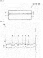
- Fig. 1 shows a view schematically illustrating a cross-sectional configuration of a bonded substrate 10 (10A, 10B) according to an embodiment of the present invention.
- the bonded substrate 10 is a substrate on which a power semiconductor not illustrated in the drawings, such as a switching element, an IGBT, or a MOSFET, for example, is mounted in a power semiconductor module including the power semiconductor.
- the bonded substrate 10 generally has a configuration in which a copper plate 3 is bonded to one main surface of a ceramic substrate 1 through a bonding layer 2.
- a bonded substrate 10 is obtained by spreading a brazing material in a paste form containing at least Ag and Ti onto one main surface of the ceramic substrate 1, thereafter superposing the copper plate 3 onto the surface on which the brazing material has been applied, and heating and pressurizing in vacuum or in an Ar atmosphere (by heated and pressurized bonding in vacuum or in an Ar atmosphere).
- the bonded substrate 10 has a configuration in which the bonding layer 2 is adjacent to both the ceramic substrate 1 and the copper plate 3 at different interfaces. In Fig. 1 , it is assumed that the ceramic substrate 1 and the bonding layer 2 form an interface I1, and the bonding layer 2 and the copper plate 3 form an interface 12.
- a nitride ceramic substrate such as a silicon nitride (Si 3 N 4 ) substrate or an aluminum nitride (A1N) substrate is exemplified.
- the planar shape and size of the ceramic substrate 1 are not particularly limited; however, from the viewpoint of achieving scale reduction of the power semiconductor module, a ceramic substrate 1 having a rectangular shape in a plan view with one side being about 20 mm to 70 mm long and with a thickness of 0.1 mm to 1.0 mm is exemplified.
- the copper plate 3 may have a planar size equal to the planar size of the ceramic substrate 1 or may have a planar size slightly smaller than the planar size of the ceramic substrate 1.
- the configuration illustrated in Fig. 1 corresponds to the former case. In the latter case, an outer peripheral part of the ceramic substrate 1 is exposed without being bonded to the copper plate 3. Meanwhile, the thickness is preferably about 0.5 mm to 2.0 mm from the viewpoint of achieving scale reduction of the power semiconductor module.
- the power semiconductor is mounted on a non-bonded surface (a main surface opposite to the side where the bonding layer 2 is present) of the copper plate 3 constituting the bonded substrate 10.
- the copper plate 3 may be prepared as a circuit substrate having an electric circuit pattern formed on itself, and the power semiconductor may be mounted on the electric circuit pattern.
- the copper plate is generally referred to simply as a copper plate 3, including a circuit substrate on which such an electric circuit pattern is formed.
- the bonding layer 2 is a layer containing TiN as a major component. Such a bonding layer 2 is made of by Ti contained as an active metal in the brazing material and N constituting the ceramic substrate 1, in the process of the above-described heated and pressurized bonding.
- the bonding layer 2 is generally formed to have a thickness of submicron order to about several ⁇ m. However, the bonding layer 2 is not necessarily formed to have a uniform thickness due to having a smaller thickness as compared with the surface undulation of the ceramic substrate 1 and the copper plate 3, and there may be variation (in-layer variation) depending on the places.
- Fig. 2 and Fig. 3 show a cross-sectional view schematically illustrating a fine structure in an interface region between the bonding layer 2 and the copper plate 3 of the bonded substrate 10 (10A, 10B) according to the present embodiment.
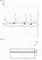
- Fig. 4 shows a view schematically illustrating a cross-sectional configuration of a bonded substrate 20 having a configuration different from that of the bonded substrate 10 according to the present embodiment, which is shown for comparison.
- Fig. 5 shows a cross-sectional view schematically illustrating a fine structure in an interface region from the bonding layer 2 to the copper plate 3 of the bonded substrate 20.
- the bonded substrate 10 and the bonded substrate 20 are both obtained by subjecting the ceramic substrate 1 and the copper plate 3 to heated and pressurized bonding using a brazing material containing Ag in addition to Ti; however, the bonded substrate 10 and the bonded substrate 20 are fabricated to be different from each other by making the bonding conditions different during the bonding.
- the brazing material it is possible to use one in which Cu, Sn, In, or the like has been added for lowering the melting point, or one in which Ti has been added to an alloy powder of these.
- an Ag-Cu-Ti-based brazing material one that contains Ag, Cu, and Ti in a composition weight ratio of 30 to 70%, 0 to 40%, and 0.1 to 20%, respectively, can be exemplified, and it is also possible to use a commercially available one that satisfies these composition ranges.
- the bonding layer 2 is in direct contact with the copper plate 3.
- Ag atoms are distributed in the copper plate 3, at least in a vicinity of an interface I2 to the bonding layer 2, as schematically illustrated by dots in Fig. 2 and Fig. 3 .
- the Ag atoms are distributed in a mode in which the concentration becomes smaller according as the distance from the interface I2 becomes larger (according as the distance to the non-bonded surface of the copper plate 3 becomes smaller).
- Fig. 2 and Fig. 3 are illustrated such that the dots are more densely distributed in a region having a larger abundance ratio of the Ag atoms.
- the Ag atoms existing in the copper plate 3 are none other than those that have been originally contained in the brazing material but have been diffused (solid-dissolved) into the copper plate 3 that is in a solid state, in the process of heated and pressurized bonding.
- the abundance ratio (solid dissolution ratio) of the Ag atoms in the Ag distribution region 3d is at most 15 at% at the maximum.
- the bonded substrate 20 is common to the bonded substrate 10 in that the Ag distribution region 3d is formed in the copper plate 3; however, the bonded substrate 20 is different from the bonded substrate 10 in that the bonding layer 2 and the copper plate 3 do not directly constitute an interface and that an Ag-Cu layer (layer made of an Ag-Cu alloy) 6, which should be referred to as a subbonding layer, intervenes therebetween.
- the Ag-Cu layer 6 is formed approximately over the entire surface of the bonding layer 2.
- the Ag-Cu layer 6 is made of both of or either one of an Ag-rich phase and a Cu-rich phase.
- the Ag-rich phase is an Ag-Cu alloy in which Ag is contained at 80% or more, the rest being Cu.
- the Cu-rich phase is an Ag-Cu alloy in which Cu is contained at 80 to 96%, the rest being Ag.
- the compositions of both the Ag-rich phase and the Cu-rich phase may vary from the above-described composition ratio when a brazing material additive (Sn, In, or the like) is contained.
- the distribution state of the Ag atoms that is, the diffusion of Ag, the presence or absence of the Ag-Cu layer 6, and the like in the copper plate 3 can be confirmed, for example, by analyzing the composition distribution using the cross-section of the bonded substrates 10 and 20 as a target by EPMA.
- the Ag distribution region 3d in the copper plate 3 is a region formed in such a manner that Ag in the brazing material is diffused into the copper plate 3 that maintains a solid state even during the process of heated and pressurized bonding, so that the matrix of crystal lattice in the region is basically constituted of Cu atoms, and the content of Ag is slight.
- the Ag-Cu layer 6 is formed in such a manner that the Ag atoms and the Cu atoms are alloyed during the process of heated and pressurized bonding, so that the Ag-Cu layer 6 is constituted of both of or either one of the Ag-rich phase and the Cu-rich phase, as described above.
- the crystal lattice of the Ag-Cu layer 6 (arrangement of the Ag atoms and the Cu atoms) depends on the alloy composition.
- the Ag-Cu layer 6 and the Ag distribution region 3d in the copper plate 3 are different from each other with respect to the forming process and the composition ratio thereof.
- the difference in configuration between the bonded substrate 10 and the bonded substrate 20 as described above means that the bonding conditions under which the bonded substrate 20 is formed is different from the bonding conditions under which the bonded substrate 10 is formed.
- a bonded substrate formed by bonding a ceramic substrate and another member in the case where there is a difference in thermal expansion coefficient between a ceramic plate and another member existing along the ceramic plate, when a temperature change is given to the bonded substrate, a difference is generated in thermal expansion of the ceramic plate and the other member to generate a thermal stress. If a thermal cycle is continuously applied to such a bonded substrate, this thermal stress is repeatedly generated, and material destruction occurs in the ceramic substrate at some time point to generate cracks.
- the two are common to have a configuration in which the bonding layer 2 and the ceramic substrate 1 are adjacent to each other; however, because the bonding layer 2 has a thermal expansion coefficient of approximately the same degree as that of the ceramic substrate 1, almost no thermal stress is generated between the bonding layer 2 and the ceramic substrate 1 both in the bonded substrate 10 and in the bonded substrate 20.
- the bonding layer 2 can be equated with the ceramic substrate 1 both in the bonded substrate 10 and in the bonded substrate 20 in considering the thermal stress.
- the Ag-Cu layer 6 is adjacent to the bonding layer 2 in the bonded substrate 20. Further, the copper plate 3 and the Ag-Cu layer 6 each have a thermal expansion coefficient different from that of the ceramic substrate 1. For this reason, it can be grasped that a thermal stress is generated between the copper plate 3 and the ceramic substrate 1 in the bonded substrate 10, and a thermal stress is generated between the Ag-Cu layer 6 and the ceramic substrate 1 in the bonded substrate 20.
- the copper plate 3 has a smaller proof strength (a smaller yield stress) than the Ag-Cu layer 6 against mechanical deformation, so that the thermal stress generated due to the difference in thermal expansion coefficient between the ceramic substrate 1 and the copper plate 3 in the bonded substrate 10 is smaller than the thermal stress generated due to the difference in thermal expansion coefficient between the ceramic substrate 1 and the Ag-Cu layer 6 in the bonded substrate 20.
- the bonded substrate 10 according to the present embodiment in which the ceramic substrate 1 and the copper plate 3 are bonded in a mode where the Ag-Cu layer does not intervene while using a brazing material containing Ag and Ti, has a higher reliability to the thermal cycle than the bonded substrate 20 constituted such that the Ag-Cu layer 6 intervenes.
- a fine undulation is randomly present generally on the surface of the ceramic substrate 1 and the copper plate 3 constituting the bonded substrate 10, so that the interfaces I1 and I2 formed between the two and the bonding layer 2 as a result of bonding by the brazing material also have a random undulation as viewed in a microscopic view.
- a bonded substrate 10A in which the voids 4 are present in such a mode is particularly referred to as a bonded substrate 10A.
- the bonded substrate 10 in which the Ag-rich phase 5 is present in such a mode is particularly referred to as a bonded substrate 10B.
- the Ag-rich phase 5 is an uneven distributing region of an Ag-rich Ag-Cu alloy in which the abundance ratio of Ag exceeds 60 at% and is 100 at% or less.
- the Ag-rich phase 5 is basically discretely present at the interface I2 between the bonding layer 2 and the copper plate 3
- the Ag-rich phase 5 is structurally differentiated from the Ag-Cu layer 6 that is provided in a mode of being adjacent to the entire surface of the bonding layer 2 in the bonded substrate 20.
- the bonding layer 2 and the copper plate 3 never directly constitute an interface.
- the difference in configuration between the bonded substrate 10A and the bonded substrate 10B means that the bonding conditions for obtaining the two are different, under the premise that the Ag-Cu layer 6 is not formed.
- formation of the Ag-rich phase 5 in the bonded substrate 10B can be also grasped as a situation in which the sites that may possibly become voids 4 under different bonding conditions are filled with the Ag-rich phase 5.
- the bonded substrate 10B formed to have a voidless structure by presence of the Ag-rich phase 5 at the positions that may become voids 4 tends to have a larger insulation breakdown voltage (insulation breakage voltage) than the bonded substrate 10A in which the voids 4 are incorporated.
- insulation breakage voltage insulation breakdown voltage
- the size (maximum size) of the Ag-rich phase 5 is, for example, about 0.1 ⁇ m to 3 ⁇ m in the thickness direction of the bonded substrate 10 and is, for example, about 0.1 ⁇ m to 5 ⁇ m in a plane that is perpendicular to the thickness direction.
- the area ratio of the Ag-rich phase 5 in the plane that is perpendicular to the thickness direction should be about 1% to 20%, and the interval between the Ag-rich phases 5 should be about 1 ⁇ m to 100 ⁇ m.
- the bonded substrate 10 (10A, 10B) according to the present embodiment is obtained by subjecting the ceramic substrate 1 and the copper plate 3 to heated and pressurized bonding using a brazing material containing Ag and Ti.
- a known technique can be applied; however, it is necessary to carry out the bonding at least under bonding conditions (bonding atmosphere, bonding temperature, bonding pressure, amount of spreading the brazing material) in which the Ag-Cu layer 6 is not formed.
- the bonding atmosphere it is necessary to set the bonding atmosphere to be vacuum or an Ar atmosphere because, if Ti as an active metal is oxidized or nitrided, it is inherently impossible to carry out the bonding.
- the bonding pressure is preferably 5 MPa or more. This is because, the lower the bonding pressure is, the more the Ag-Cu layer 6 and the voids 4 tend to be formed. Also, the bonding pressure is preferably 25 MPa or less. This is because, the higher the bonding pressure is, the less likely the Ag-Cu layer 6 and the voids 4 tend to be formed; however, when the bonding pressure is too high, the ceramic substrate 1 may be destroyed at the time of bonding.
- the bonding temperature it is preferable to set the bonding temperature to be about 800°C to 1000°C in view of using a brazing material containing Ag and Ti.
- a temperature range from 800°C to 1000°C the higher the bonding temperature is, the less likely the Ag-Cu layer 6 tends to be formed, and the lower the bonding temperature is, the more likely the Ag-Cu layer 6 tends to be formed.
- the application amount (application thickness) of the brazing material it is preferable to define the application amount (application thickness) of the brazing material so that the thickness of the bonding layer obtained after bonding becomes 0.1 ⁇ m to 5 ⁇ m.
- the bonding pressure is set to be 5 MPa to 25 MPa; the bonding temperature is set to be 850°C; and the application amount (application thickness) of the brazing material is defined so that the thickness of the bonding layer obtained after bonding becomes 0.1 ⁇ m to 5 ⁇ m, a voidless bonded substrate 10B is obtained in which the Ag-rich phase 5 is discretely present while the Ag-Cu layer 6 is not formed.
- the bonding pressure is set to be 1 MPa to 1.5 MPa; the bonding temperature is set to be 800°C; and the application amount (application thickness) of the brazing material is defined so that the thickness of the bonding layer obtained after bonding becomes 10 ⁇ m to 20 ⁇ m, the Ag-Cu layer 6 is eventually formed (the bonded substrate 20 is obtained).
- the bonding pressure is set to be 5 MPa to 25 MPa; the bonding temperature is set to be 950°C; and the application amount (application thickness) of the brazing material is defined so that the thickness of the bonding layer obtained after bonding becomes 0.1 ⁇ m to 5 ⁇ m, a bonded substrate 10A is obtained in which voids 4 are present though both the Ag-Cu layer 6 and the Ag-rich phase 5 are not formed. This seems to be because, in the case of such bonding conditions, the Ag atoms do not remain between the bonding layer 2 and the copper plate 3 but are diffused into the copper plate 3.
- a bonded substrate having a high reliability to a thermal cycle and having an excellent heat-dissipating property can be obtained by allowing the bonded substrate obtained by subjecting a ceramic substrate and a copper plate to heated and pressurized bonding using an Ag-Cu-Ti-based brazing material to have a configuration in which Ag is diffused into the copper plate while an Ag-Cu layer does not intervene between the bonded layer made of TiN and the copper plate.
- a bonded substrate having a high reliability not only to a thermal cycle but also to electric insulation breakage can be obtained by allowing the interface between the bonding layer and the copper plate in the bonded substrate in which such an Ag-Cu layer does not intervene, to have a configuration in which the Ag-rich phase is discretely present while voids are absent.
- the bonded substrate is configured by bonding the copper plate 3 onto one main surface side of the ceramic substrate 1.
- the bonded substrate may be configured by bonding the copper plate 3 also onto the other main surface side in a mode similar to that of the above-described embodiment.
- the bonded substrate may be configured by bonding the copper plate 3 to both the two main surfaces of the ceramic substrate 1.
- Example 1 to Example 6 bonded substrates 10A at six levels in which the combination of the material and thickness of the ceramic substrate 1 and the thickness of the copper plate (Cu plate) 3 was varied in various ways were fabricated by heated and pressurized bonding.
- the material of the ceramic substrate 1 was set to be silicon nitride (Si 3 N 4 ) or aluminum nitride (A1N).
- Si 3 N 4 silicon nitride
- A1N aluminum nitride
- the thickness of the copper plate 3 was varied to five levels of 0.3 mm, 0.6 mm, 1 mm, 1.5 mm, and 2.0 mm for the case where the ceramic substrate 1 was the silicon nitride (Si 3 N 4 ) substrate.
- the thickness of the copper plate 3 was set be 0.3 mm for the case where the ceramic substrate 1 was the aluminum nitride (A1N) substrate.
- Example 7 to Example 12 bonded substrates 10B at six levels in which the combination of the material and thickness of the ceramic substrate 1 and the thickness of the copper plate 3 was set to be the same as in Example 1 to Example 6 were fabricated by heated and pressurized bonding.
- bonded substrates 20 at six levels in which the combination of the material and thickness of the ceramic substrate 1 and the thickness of the copper plate 3 was set to be the same as in Example 1 to Example 6 were fabricated by heated and pressurized bonding.
- Example 1 to Example 12 and Comparative Example 1 to Comparative Example 6 as the brazing material to be used in heated and pressurized bonding, one having a composition weight ratio of Ag: 51%, Cu: 24%, In: 11%, and Ti: 14% was used, and the bonding atmosphere was set to be vacuum.
- Example 1 to Example 6 the amount of spreading the brazing material was defined so that the thickness of the bonding layer obtained after bonding would be within a range of 0.1 ⁇ m to 3 ⁇ m in terms of in-layer variation.
- Example 7 to Example 12 the amount of spreading the brazing material was defined so that the thickness of the bonding layer obtained after bonding would be within a range of 0.1 ⁇ m to 3 ⁇ m in terms of in-layer variation.
- the amount of spreading the brazing material was defined so that the thickness of the bonding layer obtained after bonding would be within a range of 13 ⁇ m to 20 ⁇ m in terms of such in-layer variation.
- the bonding pressure for Example 1 to Example 12 was set to be 20 MPa
- the bonding pressure for Comparative Example 1 to Comparative Example 6 was set to be 1 MPa which was a less heavy load than that for Example 1 to Example 12.
- bonded substrates 30 at six levels were obtained by forming a Ti film having a value of thickness within a range of 10 nm to 100 nm on the ceramic substrate 1 instead of using a brazing material while setting the combination of the material and thickness of the ceramic substrate 1 and the thickness of the copper plate 3 to be the same as in Example 1 to Example 6, superposing the copper plate 3 on the Ti film, and performing heated and pressurized bonding.
- the bonding atmosphere was set to be vacuum.
- the bonding temperature was set to be 1000°C, and the bonding pressure was set to be 20 MPa.
- Fig. 6 shows a cross-sectional view schematically illustrating a fine structure in an interface region between a bonding layer 7 and a copper plate 3 of such a bonded substrate 30.
- the ceramic substrate 1 and the copper plate 3 are bonded by the bonding layer 7.
- voids 4 are present at an interface part between the copper plate 3 and the bonding layer 7.
- a cut surface obtained by cutting perpendicularly to the bonding surface was observed with an electron microscope, so as to confirm the presence or absence of an Ag-Cu layer that was continuous to the bonding layer between the bonding layer and the copper plate, and to confirm the presence or absence of an Ag-rich phase.
- the observation was carried out at three sites as a target including the right and left ends and the central part in the substrate in-plane direction of the cut surface.
- the observation magnification ratio was set to be 1000 times, and the observation width at each site in the substrate in-plane direction was set to be 0.1 mm. In such a case, a region in which Ag was unevenly present with a thickness of 0.5 ⁇ m to 3 ⁇ m and a width of 0.5 ⁇ m to 5 ⁇ m was determined as an Ag-rich phase.
- composition mapping was carried out with an EDS at each observation site of the cut surface with respect to an area of 10 ⁇ m of the copper plate 3 in the thickness direction from the bonding interface between the bonding layer 2 and the copper plate 3.
- Table 1 shows a list of the conditions of the ceramic substrate and the copper plate (Cu plate), presence or absence of the Ag-Cu layer that is continuous to the bonding layer, presence or absence of Ag diffusion into the copper plate (Cu plate), and the Ag-rich phase in the bonded substrates according to Example 1 to Example 12 and Comparative Example 1 to Comparative Example 12.
- Example 1 to Example 12 were common to each other in that the Ag-Cu layer that was continuous to the bonding layer was absent and that Ag was diffused into the copper plate 3. However, in Example 1 to Example 6, the Ag-rich phase was absent, whereas in Example 7 to Example 12, the Ag-rich phase was present.
- Example 1 to Example 6 voids were present at the interface between the bonding layer and the copper plate. Also, the mode of distribution of the Ag-rich phase in Example 7 to Example 12 was similar to the mode of distribution of the voids in Example 1 to Example 6.
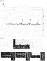
- Fig. 7 shows a view showing together an SEM image (upper stage) with respect to an interface vicinity of Example 9 and an EPMA element mapping image (lower stage) with respect to Ti, Ag, and Cu. From Fig.
- Comparative Example 7 to Comparative Example 12 the Ag-Cu layer that was continuous to the bonding layer was absent likewise in Example 1 to Example 12; however, Comparative Example 7 to Comparative Example 12 were different from Example 1 to Example 12 in that the diffusion of Ag into the copper plate was not confirmed.
- Example 1 to Example 12 With respect to each of the bonded substrates according to Example 1 to Example 12 and Comparative Example 1 to Comparative Example 12, a thermal cycle test was carried out. In each of the Examples and Comparative Examples, the number of test samples was set to be five. The test was carried out by giving to each sample a thermal cycle of -55°C (15 minutes) / 150°C (15 minutes) for 3000 cyc (cycles), during which, for every 100 cycles (that is, for a total of 30 times), confirmation was made on peeling-off of the bonding part and presence or absence of cracks in the ceramic substrate (hereafter, these are generally referred to as "destruction" together) by an outer appearance confirmation with a stereoscopic microscope and ultrasonic flaw detection.
- Table 2 shows a list of the evaluation timing at which the destruction was confirmed (how many times of evaluation at which the destruction was confirmed) in the thermal cycle test with respect to all the samples of the bonded substrates according to Example 1 to Example 12 and Comparative Example 1 to Comparative Example 12, and an average value for the respective five samples. For example, if the destruction was confirmed at the 29th evaluation timing, it means that the destruction occurred between the 2800th cycle and the 2900th cycle. A sample in which no destruction was confirmed at the 30th evaluation after giving 3000 cycles of the thermal cycle is denoted as "not confirmed”.
- Example 1 to Example 5 and Example 7 to Example 11 in which silicon nitride (Si 3 N 4 ) was used as the ceramic substrate the destruction was confirmed generally at the 25th evaluation timing and afterwards.
- the destruction was not confirmed even at the 30th evaluation timing after giving 3000 cycles of the thermal cycle in all the samples.
- Example 6 and Example 12 in which aluminum nitride (A1N) was used as the ceramic substrate the destruction was confirmed at the 16th to 17th evaluation timing in average.
- a thermal resistance measurement was carried out on each of the bonded substrates according to Example 1 to Example 12 and Comparative Example 1 to Comparative Example 12 as a target.
- a bonded substrate was prepared in which a copper plate having a plane size of 20 mm ⁇ 20 mm had been bonded to both surfaces of a ceramic substrate having a plane size of 21 mm ⁇ 21 mm under the conditions according to each Example or Comparative Example.
- a semiconductor chip having a size of 8 mm ⁇ 8 mm was mounted by soldering at the center on one side of the bonded substrate. Then, the other surface of copper plate that is opposite to the semiconductor chip mounting surface with the ceramic substrate sandwiched therebetween was bonded by soldering onto a copper base plate having a plane size of 50 mm ⁇ 50 mm and a thickness of 4 mm, and the copper base plate was disposed on a cooling plate via a thermal grease to obtain a module for evaluation.
- the measurement was carried out in accordance with the standard JESD51-14 of JEDEC. In each of the Examples and Comparative Examples, the number of test samples was set to be five.
- Table 3 shows a list of the result of thermal resistance measurement with respect to all the samples of the bonded substrates according to Example 1 to Example 12 and Comparative Example 1 to Comparative Example 12 and an average value for the respective five samples.
- Thermal resistance measurement result (unit: K/W)
- Example 1 Example 2
- Example 3 Example 4
- Example 6 #1 0.151 0.148 0.135 0.137 0.137 0.204 #2 0.145 0.141 0.138 0.140 0.134 0.201 #3 0.153 0.147 0.139 0.135 0.139 0.203 #4 0.155 0.149 0.137 0.139 0.132 0.206 #5 0.148 0.146 0.139 0.140 0.133 0.201 Average 0.150 0.1 46 0.138 0.138 0.135 0.203
- Example 7 Example 8
- Example 10 Example 11
- Example 12 #1 0.154 0.149 0.139 0.138 0.138 0.208 #2 0.149 0.143 0.139 0.141 0.137 0.202 #3 0.155 0.151 0.139 0.138 0.139 0.204 #4 0.155 0.151 0.139 0.142 0.137 0.206 #5 0.148 0.151 0.139 0.141 0.137 0.204 Average 0.152 0.149 0.139 0.
- Example 1 to Example 5 As shown in Table 3, among the bonded substrates in which silicon nitride (Si 3 N 4 ) was used as the ceramic substrate, in Example 1 to Example 5, Example 7 to Example 11, and Comparative Example 1 to Comparative Example 5 in which diffusion of Ag into the copper plate occurred, the value of thermal resistance is approximately about 0.135 K/W to 0.15 K/W, whereas in Comparative Example 7 to Comparative Example 11 in which diffusion of Ag into the copper plate did not occur, the value of thermal resistance tends to be as high as approximately about 0.25 K/W to 0.28 K/W.
- Example 6 Example 12, and Comparative Example 6 (the value of thermal resistance is approximately about 0.20 K/W to 0.21 K/W), and Comparative Example 12 (the value of thermal resistance is approximately about 0.334 K/W to 0.341 K/W) all of which aluminum nitride (A1N) was used as the ceramic substrate, though the absolute values are different.
- A1N aluminum nitride
- An insulation breakdown voltage (insulation breakage voltage) measurement was carried out on each of the bonded substrates according to Example 1 to Example 12 as a target.
- the number of test samples was set to be ten.
- the measurement was carried out by applying an alternating-current voltage between a non-bonded surface of the copper plate serving as a circuit surface of the bonded substrate and a non-bonded surface of the ceramic substrate serving as a heat-dissipating surface, in an insulating oil.
- Table 4 shows a list of the result of measurement of insulation breakdown voltage as well as an average value with respect to all the samples of the bonded substrates according to Example 1 to Example 12 and standard deviation ⁇ for the respective ten samples.
- Insulation breakdown voltage measurement result (unit: kV/mm)
- Example 1 Example 2
- Example 3 Example 4
- Example 5 Example 6 #1 6.0 9.3 5.5 10.3 9.4 7.2 #2 6.9 8.6 8.7 7.9 10.6 6.7 #3 8.0 6.5 9.1 10.0 9.3 8.3 #4 5.1 7.9 6.2 9.0 6.4 6.7 #5 5.0 9.5 6.3 5.4 7.9 7.9 #6 9.2 5.3 8.8 7.7 5.8 6.0 #7 7.2 6.5 5.9 6.0 6.5 6.6 #8 6.5 8.1 6.9 5.6 10.3 6.0 #9 5.9 7.4 5.8 6.0 9.3 6.4 #10 9.4 7.8 9.9 7.4 7.7 6.0 Average 6.9 7.7 7.3 7.5 8.3 6.8 ⁇ 1.6 2.0 1.6 1.8 1.7 2.1
- Example 7 Example
- Example 1 to Example 6 in which the Ag-rich phase was not confirmed while voids were confirmed at the interface between the bonding layer and the copper plate, the average value of the insulation breakdown voltage was 8.3 kV/ mm at the maximum, and the value of ⁇ was 1.6 kV/mm at the minimum.
- Example 7 to Example 12 in which the Ag-rich phase was confirmed while voids were not confirmed at the interface between the bonding layer and the copper plate, the average value of the insulation breakdown voltage was 8.8 kV/mm at the minimum, and the value of ⁇ was 1.3 kV/mm at the maximum.
Description
- The present invention relates to a substrate on which a power semiconductor is mounted, and particularly to a bonded substrate in which a copper plate is bonded to a ceramic substrate by using a brazing material. The document
US2014/291385A is a closely related prior art. - A power semiconductor module is used for electric power control of an HEV/EV, an electric railcar, or the like. The power semiconductor module is composed of, for example, an electric circuit for mounting a power semiconductor such as a switching element, an IGBT, or a MOSFET, as well as an insulating heat-dissipating substrate, a cooling member, and a case body. The power semiconductor module is highly heat-generative because of performing a large electric power control and also is used under a thermal cycle environment. For this reason, reliability (durability) to the thermal cycle is demanded in addition to electric insulation property and heat-dissipating property in the insulating heat-dissipating substrate on which the power semiconductor is mounted.
- Conventionally, as an insulating heat-dissipating substrate, there has been widely known a DCB substrate in which a thin copper plate is directly bonded to an alumina substrate, an aluminum nitride substrate, a silicon nitride substrate, or the like. Also, a mode has been already known in which a silicon nitride substrate and a copper plate are bonded by the diffusion bonding method (for example, see Non-Patent Literature 1).
- Furthermore, as an insulating heat-dissipating substrate, there has been widely known an AMB substrate in which a thin copper plate and a ceramic substrate such as an alumina substrate, an aluminum nitride substrate, or a silicon nitride substrate are bonded through a bonding layer formed by using a brazing material (bonding material) containing an active metal. As the AMB substrate, one in which the bonding layer has been formed with use of a brazing material containing Ag (for example, see
Patent Literature 1 and Patent Literature 2) and one in which the bonding layer has been formed with use of a brazing material not containing Ag (for example, seePatent Literature 3 and Patent Literature 4) are both known. - Also, heated and pressurized bonding has been already known as a technique for bonding an insulating substrate and a metal plate (circuit substrate) with a brazing material (for example, see
Patent Literature 5 to Patent Literature 9). - In recent years, improvement in output density as well as scale reduction have been demanded in the power semiconductor modules. By receiving such a demand, studies have been made on increasing the thickness of the copper plate for the purpose of satisfying both of the heat-dissipating property and the scale reduction in the insulating heat-dissipating substrate used in the power semiconductor modules.
- However, in the case that a thick copper plate is used, a heat stress generated at the bonding end of the copper plate and the ceramic substrate increases due to the thermal expansion difference between copper and ceramics, thereby raising a problem that cracks are generated in the ceramic substrate because of the residual heat stress generated by the heat treatment at the time of bonding the ceramic substrate and the copper plate and the repeated heat stress generated by temperature change at the time of actual use.
- The inventors of the present invention have found out, as a result of eager studies, that in an AMB substrate whose bonding layer is formed by using a brazing material containing Ag, the mode of presence of Ag in a vicinity of the interface between the copper plate and the bonding layer exerts an influence on the reliability to the thermal cycle.
- None of
Patent Literature 1,Patent Literature 2, andPatent Literature 5 to Patent Literature 9 discloses or suggests the relationship between the thermal cycle and the mode of presence of Ag in a vicinity of the interface between the copper plate and the bonding layer in the AMB substrate. - For example,
Patent Literature 1 discloses merely a technique of attaining improvement in the heat-resistant cycle by disposing a brazing material extrusion part with few defects such as voids. - Also,
Patent Literature 2 discloses merely a technique of improving the heat-resistant cycle property by adjusting the composition of the silicon nitride substrate itself and the number of grain boundaries. -
- PTL 1: Japanese Patent Application Laid-open No.
2014-207482 - PTL 2: Japanese Patent No.
3629783 - PTL 3: Japanese Patent Application Laid-open No.
2003-283064 - PTL 4: Japanese Patent Application Laid-open No.
05-32463 - PTL 5: Japanese Patent Application Laid-open No.
2002-43482 - PTL 6: Japanese Patent Application Laid-open No.
2002-359453 - PTL 7: Japanese Patent Application Laid-open No.
2004-253736 - PTL 8: Japanese Patent No.
4015023 - PTL 9: Japanese Patent No.
4014528 - NPL 1: "Development of Highly Reliable Cooling (Heat-Dissipating) Substrate for SiC Element by Diffusion Bonding Method", Strategic Foundational Technology Upgrading Support Program, Research Development Result Example Cases, Adopted Programs of the year H.24 to H.25, Kanto Bureau of Economy, Trade and Industry, Industries Department, Manufacturing Industries Division, issued in March, 2015, p. 28-29.
- The present invention has been made in view of the aforementioned problems, and an object thereof is to provide a bonded substrate mainly for mounting a power semiconductor in which the reliability to a thermal cycle has been enhanced as compared with a conventional one.
- In order to solve the aforementioned problems, a first aspect of the present invention provides a bonded substrate including a copper plate bonded to one or both main surface(s) of a nitride ceramic substrate, wherein a bonding layer consisting of TiN intervenes between the nitride ceramic substrate and the copper plate and is adjacent at least to the copper plate, and an Ag distribution region is present in the copper plate.
- Also, a second aspect of the present invention provides the bonded substrate according to the first aspect, wherein an Ag-rich phase is present discretely at an interface between the bonding layer and the copper plate.
- Also, a third aspect of the present invention provides the bonded substrate according to the first or second aspect, wherein the Ag distribution region is present in the copper plate to be in contact with an interface between the copper plate and the bonding layer.
- Also, a fourth aspect of the present invention provides a method for manufacturing a bonded substrate including a copper plate bonded to one or both main surface(s) of a nitride ceramic substrate, the method comprising an application step of spreading a brazing material paste containing at least Ag and Ti to one or both main surface(s) of the nitride ceramic substrate and a bonding step of heating and pressurizing the copper plate and the nitride ceramic substrate in vacuum or in an Ar atmosphere in a state in which the copper plate is superposed onto the surface(s) of the nitride ceramic substrate where the brazing material paste has been applied, wherein, by performing the application step and the bonding step, in the bonded substrate, a bonding layer consisting of TiN is generated between the nitride ceramic substrate and the copper plate so as to be adjacent at least to the copper plate, and Ag contained in the brazing material paste is diffused in the copper plate to form an Ag distribution region in the copper plate.
- Also, a fifth aspect of the present invention provides the method for manufacturing a bonded substrate according to the fourth aspect, wherein, by performing the application step and the bonding step, further in the bonded substrate, an Ag-rich phase is made to be present discretely at an interface between the bonding layer and the copper plate.
- According to the first to fifth aspects of the present invention, there can be obtained a bonded substrate having a high reliability to a thermal cycle and being excellent in the heat-dissipation property.
- In particular, according to the second and fifth aspects, there can be obtained a bonded substrate having a high reliability not only to a thermal cycle but also to electric insulation breakdown.
-
- [
fig.1]Fig. 1 shows a view schematically illustrating a cross-sectional configuration of a bonded substrate 10 (10A, 10B) according to an embodiment of the present invention. - [
fig.2]Fig. 2 shows a cross-sectional view schematically illustrating a fine structure in an interface region between abonding layer 2 and acopper plate 3 of thebonded substrate 10A. - [
fig.3]Fig. 3 shows a cross-sectional view schematically illustrating a fine structure in an interface region between abonding layer 2 and acopper plate 3 of thebonded substrate 10B. - [
fig.4]Fig. 4 shows a view schematically illustrating a cross-sectional configuration of a bondedsubstrate 20. - [
fig.5]Fig. 5 shows a cross-sectional view schematically illustrating a fine structure in an interface region from abonding layer 2 to acopper plate 3 of thebonded substrate 20. - [
fig.6]Fig. 6 shows a cross-sectional view schematically illustrating a fine structure in an interface region between a bonding layer 7 and acopper plate 3 of a bondedsubstrate 30. - [
fig.7]Fig. 7 shows a view showing together an SEM image with respect to an interface vicinity of Example 9 and an EPMA element mapping image with respect to Ti, Ag, and Cu. -
Fig. 1 shows a view schematically illustrating a cross-sectional configuration of a bonded substrate 10 (10A, 10B) according to an embodiment of the present invention. Thebonded substrate 10 is a substrate on which a power semiconductor not illustrated in the drawings, such as a switching element, an IGBT, or a MOSFET, for example, is mounted in a power semiconductor module including the power semiconductor. - The bonded
substrate 10 generally has a configuration in which acopper plate 3 is bonded to one main surface of aceramic substrate 1 through abonding layer 2. Such a bondedsubstrate 10 is obtained by spreading a brazing material in a paste form containing at least Ag and Ti onto one main surface of theceramic substrate 1, thereafter superposing thecopper plate 3 onto the surface on which the brazing material has been applied, and heating and pressurizing in vacuum or in an Ar atmosphere (by heated and pressurized bonding in vacuum or in an Ar atmosphere). In other words, thebonded substrate 10 has a configuration in which thebonding layer 2 is adjacent to both theceramic substrate 1 and thecopper plate 3 at different interfaces. InFig. 1 , it is assumed that theceramic substrate 1 and thebonding layer 2 form an interface I1, and thebonding layer 2 and thecopper plate 3 form aninterface 12. - As the
ceramic substrate 1, a nitride ceramic substrate such as a silicon nitride (Si3N4) substrate or an aluminum nitride (A1N) substrate is exemplified. In realizing the present invention, the planar shape and size of theceramic substrate 1 are not particularly limited; however, from the viewpoint of achieving scale reduction of the power semiconductor module, aceramic substrate 1 having a rectangular shape in a plan view with one side being about 20 mm to 70 mm long and with a thickness of 0.1 mm to 1.0 mm is exemplified. - The
copper plate 3 may have a planar size equal to the planar size of theceramic substrate 1 or may have a planar size slightly smaller than the planar size of theceramic substrate 1. The configuration illustrated inFig. 1 corresponds to the former case. In the latter case, an outer peripheral part of theceramic substrate 1 is exposed without being bonded to thecopper plate 3. Meanwhile, the thickness is preferably about 0.5 mm to 2.0 mm from the viewpoint of achieving scale reduction of the power semiconductor module. - In more detail, the power semiconductor is mounted on a non-bonded surface (a main surface opposite to the side where the
bonding layer 2 is present) of thecopper plate 3 constituting thebonded substrate 10. In such a case, thecopper plate 3 may be prepared as a circuit substrate having an electric circuit pattern formed on itself, and the power semiconductor may be mounted on the electric circuit pattern. However, in the following description, the copper plate is generally referred to simply as acopper plate 3, including a circuit substrate on which such an electric circuit pattern is formed. - The
bonding layer 2 is a layer containing TiN as a major component. Such abonding layer 2 is made of by Ti contained as an active metal in the brazing material and N constituting theceramic substrate 1, in the process of the above-described heated and pressurized bonding. Thebonding layer 2 is generally formed to have a thickness of submicron order to about several µm. However, thebonding layer 2 is not necessarily formed to have a uniform thickness due to having a smaller thickness as compared with the surface undulation of theceramic substrate 1 and thecopper plate 3, and there may be variation (in-layer variation) depending on the places. -
Fig. 2 andFig. 3 show a cross-sectional view schematically illustrating a fine structure in an interface region between thebonding layer 2 and thecopper plate 3 of the bonded substrate 10 (10A, 10B) according to the present embodiment. - On the other hand,
Fig. 4 shows a view schematically illustrating a cross-sectional configuration of a bondedsubstrate 20 having a configuration different from that of the bondedsubstrate 10 according to the present embodiment, which is shown for comparison. Further,Fig. 5 shows a cross-sectional view schematically illustrating a fine structure in an interface region from thebonding layer 2 to thecopper plate 3 of the bondedsubstrate 20. - The bonded
substrate 10 and the bondedsubstrate 20 are both obtained by subjecting theceramic substrate 1 and thecopper plate 3 to heated and pressurized bonding using a brazing material containing Ag in addition to Ti; however, the bondedsubstrate 10 and the bondedsubstrate 20 are fabricated to be different from each other by making the bonding conditions different during the bonding. - Here, as the brazing material, it is possible to use one in which Cu, Sn, In, or the like has been added for lowering the melting point, or one in which Ti has been added to an alloy powder of these. For example, as an Ag-Cu-Ti-based brazing material, one that contains Ag, Cu, and Ti in a composition weight ratio of 30 to 70%, 0 to 40%, and 0.1 to 20%, respectively, can be exemplified, and it is also possible to use a commercially available one that satisfies these composition ranges.
- In the bonded
substrate 10, as illustrated inFig. 1 , thebonding layer 2 is in direct contact with thecopper plate 3. - In addition, although illustration has been omitted in the schematic view of
Fig. 1 , in the bondedsubstrate 10, Ag atoms are distributed in thecopper plate 3, at least in a vicinity of an interface I2 to thebonding layer 2, as schematically illustrated by dots inFig. 2 andFig. 3 . The Ag atoms are distributed in a mode in which the concentration becomes smaller according as the distance from the interface I2 becomes larger (according as the distance to the non-bonded surface of thecopper plate 3 becomes smaller). Here,Fig. 2 andFig. 3 are illustrated such that the dots are more densely distributed in a region having a larger abundance ratio of the Ag atoms. - In view of the process of fabricating the bonded
substrate 10 in which theceramic substrate 1 and thecopper plate 3 are bonded by using a brazing material, and in view of the mode of distribution of the Ag atoms in thecopper plate 3, the Ag atoms existing in thecopper plate 3 are none other than those that have been originally contained in the brazing material but have been diffused (solid-dissolved) into thecopper plate 3 that is in a solid state, in the process of heated and pressurized bonding. - In other words, this means that the heated and pressurized bonding for obtaining the bonded
substrate 10 according to the present embodiment is carried out under conditions such that thebonding layer 2 consisting of TiN is formed between theceramic substrate 1 and thecopper plate 3 and that anAg distribution region 3d is formed in thecopper plate 3, at least in a vicinity of the interface I2 to thebonding layer 2. However, the abundance ratio (solid dissolution ratio) of the Ag atoms in theAg distribution region 3d is at most 15 at% at the maximum. - Because Ag has a higher thermal conductivity than Cu, formation of the
Ag distribution region 3d in thecopper plate 3 produces an effect of reducing the heat resistance of the bondedsubstrate 10 and improving the heat-dissipating property. - Meanwhile, the bonded
substrate 20 is common to the bondedsubstrate 10 in that theAg distribution region 3d is formed in thecopper plate 3; however, the bondedsubstrate 20 is different from the bondedsubstrate 10 in that thebonding layer 2 and thecopper plate 3 do not directly constitute an interface and that an Ag-Cu layer (layer made of an Ag-Cu alloy) 6, which should be referred to as a subbonding layer, intervenes therebetween. The Ag-Cu layer 6 is formed approximately over the entire surface of thebonding layer 2. The Ag-Cu layer 6 is made of both of or either one of an Ag-rich phase and a Cu-rich phase. The Ag-rich phase is an Ag-Cu alloy in which Ag is contained at 80% or more, the rest being Cu. The Cu-rich phase is an Ag-Cu alloy in which Cu is contained at 80 to 96%, the rest being Ag. The compositions of both the Ag-rich phase and the Cu-rich phase may vary from the above-described composition ratio when a brazing material additive (Sn, In, or the like) is contained. - Here, the distribution state of the Ag atoms, that is, the diffusion of Ag, the presence or absence of the Ag-
Cu layer 6, and the like in thecopper plate 3 can be confirmed, for example, by analyzing the composition distribution using the cross-section of the bondedsubstrates - Speaking in a confirming manner, the
Ag distribution region 3d in thecopper plate 3 is a region formed in such a manner that Ag in the brazing material is diffused into thecopper plate 3 that maintains a solid state even during the process of heated and pressurized bonding, so that the matrix of crystal lattice in the region is basically constituted of Cu atoms, and the content of Ag is slight. In contrast, the Ag-Cu layer 6 is formed in such a manner that the Ag atoms and the Cu atoms are alloyed during the process of heated and pressurized bonding, so that the Ag-Cu layer 6 is constituted of both of or either one of the Ag-rich phase and the Cu-rich phase, as described above. For this reason, the crystal lattice of the Ag-Cu layer 6 (arrangement of the Ag atoms and the Cu atoms) depends on the alloy composition. In other words, the Ag-Cu layer 6 and theAg distribution region 3d in thecopper plate 3 are different from each other with respect to the forming process and the composition ratio thereof. - The difference in configuration between the bonded
substrate 10 and the bondedsubstrate 20 as described above means that the bonding conditions under which the bondedsubstrate 20 is formed is different from the bonding conditions under which the bondedsubstrate 10 is formed. - Further, such a difference in configuration between the bonded
substrate 10 and the bondedsubstrate 20 gives a difference in the reliability of the two to the thermal cycle. - Generally, in a bonded substrate formed by bonding a ceramic substrate and another member, in the case where there is a difference in thermal expansion coefficient between a ceramic plate and another member existing along the ceramic plate, when a temperature change is given to the bonded substrate, a difference is generated in thermal expansion of the ceramic plate and the other member to generate a thermal stress. If a thermal cycle is continuously applied to such a bonded substrate, this thermal stress is repeatedly generated, and material destruction occurs in the ceramic substrate at some time point to generate cracks.
- With regard to the bonded
substrate 10 and the bondedsubstrate 20, the two are common to have a configuration in which thebonding layer 2 and theceramic substrate 1 are adjacent to each other; however, because thebonding layer 2 has a thermal expansion coefficient of approximately the same degree as that of theceramic substrate 1, almost no thermal stress is generated between thebonding layer 2 and theceramic substrate 1 both in the bondedsubstrate 10 and in the bondedsubstrate 20. Considering also that the thickness of thebonding layer 2 is sufficiently small as compared with theceramic substrate 1, thebonding layer 2 can be equated with theceramic substrate 1 both in the bondedsubstrate 10 and in the bondedsubstrate 20 in considering the thermal stress. - On the other hand, while the
copper plate 3 is adjacent to thebonding layer 2 in the bondedsubstrate 10, the Ag-Cu layer 6 is adjacent to thebonding layer 2 in the bondedsubstrate 20. Further, thecopper plate 3 and the Ag-Cu layer 6 each have a thermal expansion coefficient different from that of theceramic substrate 1. For this reason, it can be grasped that a thermal stress is generated between thecopper plate 3 and theceramic substrate 1 in the bondedsubstrate 10, and a thermal stress is generated between the Ag-Cu layer 6 and theceramic substrate 1 in the bondedsubstrate 20. - When the bonded
substrate 10 is compared with the bondedsubstrate 20 from this viewpoint, thecopper plate 3 has a smaller proof strength (a smaller yield stress) than the Ag-Cu layer 6 against mechanical deformation, so that the thermal stress generated due to the difference in thermal expansion coefficient between theceramic substrate 1 and thecopper plate 3 in the bondedsubstrate 10 is smaller than the thermal stress generated due to the difference in thermal expansion coefficient between theceramic substrate 1 and the Ag-Cu layer 6 in the bondedsubstrate 20. This can be stated that, when a thermal cycle is applied in the same manner, cracks are less liable to be generated in theceramic substrate 1 in the bondedsubstrate 10 according to the present embodiment than in the bondedsubstrate 20. - This means that the bonded
substrate 10 according to the present embodiment, in which theceramic substrate 1 and thecopper plate 3 are bonded in a mode where the Ag-Cu layer does not intervene while using a brazing material containing Ag and Ti, has a higher reliability to the thermal cycle than the bondedsubstrate 20 constituted such that the Ag-Cu layer 6 intervenes. - In further stating with respect to such a bonded
substrate 10, a fine undulation is randomly present generally on the surface of theceramic substrate 1 and thecopper plate 3 constituting the bondedsubstrate 10, so that the interfaces I1 and I2 formed between the two and thebonding layer 2 as a result of bonding by the brazing material also have a random undulation as viewed in a microscopic view. - In addition, in more detail, as illustrated in
Fig. 2 , there are cases wherevoids 4 are discretely present at the interface I2 between thebonding layer 2 and thecopper plate 3. Hereafter, the bondedsubstrate 10 in which thevoids 4 are present in such a mode is particularly referred to as a bondedsubstrate 10A. - Alternatively, as illustrated by hatching in
Fig. 3 , there are cases where an Ag-rich phase 5 is discretely present at theinterface 12. Hereafter, the bondedsubstrate 10 in which the Ag-rich phase 5 is present in such a mode is particularly referred to as a bondedsubstrate 10B. Here, the Ag-rich phase 5 is an uneven distributing region of an Ag-rich Ag-Cu alloy in which the abundance ratio of Ag exceeds 60 at% and is 100 at% or less. - However, in view of the fact that the Ag-
rich phase 5 is basically discretely present at the interface I2 between thebonding layer 2 and thecopper plate 3, the Ag-rich phase 5 is structurally differentiated from the Ag-Cu layer 6 that is provided in a mode of being adjacent to the entire surface of thebonding layer 2 in the bondedsubstrate 20. Unlike the former case, in the latter case, thebonding layer 2 and thecopper plate 3 never directly constitute an interface. - The difference in configuration between the bonded
substrate 10A and the bondedsubstrate 10B means that the bonding conditions for obtaining the two are different, under the premise that the Ag-Cu layer 6 is not formed. Here, formation of the Ag-rich phase 5 in the bondedsubstrate 10B can be also grasped as a situation in which the sites that may possibly becomevoids 4 under different bonding conditions are filled with the Ag-rich phase 5. - Also, such a difference in configuration gives a difference in the insulation breakdown voltage between the bonded
substrate 10A and the bondedsubstrate 10B. - Generally, when a void part is present in a bonded substrate, there is a high risk that electric field is concentrated in the void part and the void part becomes a starting point of insulation breakage. For this reason, the bonded
substrate 10B formed to have a voidless structure by presence of the Ag-rich phase 5 at the positions that may becomevoids 4 tends to have a larger insulation breakdown voltage (insulation breakage voltage) than the bondedsubstrate 10A in which thevoids 4 are incorporated. In other words, it can be stated that the bondedsubstrate 10B has a higher reliability to electric insulation breakage than the bondedsubstrate 10A. - This means that when the Ag-
rich phase 5 is allowed to be present discretely at the interface between thebonding layer 2 and thecopper plate 3 to make the interface have a voidless structure in obtaining the bonded substrate by bonding theceramic substrate 1 and thecopper plate 3 in a mode in which an Ag-Cu layer does not intervene while using a brazing material containing Ag and Ti, a bondedsubstrate 10 having a high reliability to a thermal cycle and having a high reliability to electric insulation breakage can be realized. - Here, in such a case, the size (maximum size) of the Ag-
rich phase 5 is, for example, about 0.1 µm to 3 µm in the thickness direction of the bondedsubstrate 10 and is, for example, about 0.1 µm to 5 µm in a plane that is perpendicular to the thickness direction. Also, the area ratio of the Ag-rich phase 5 in the plane that is perpendicular to the thickness direction should be about 1% to 20%, and the interval between the Ag-rich phases 5 should be about 1 µm to 100 µm. - As described above, the bonded substrate 10 (10A, 10B) according to the present embodiment is obtained by subjecting the
ceramic substrate 1 and thecopper plate 3 to heated and pressurized bonding using a brazing material containing Ag and Ti. With respect to the heated and pressurized bonding, a known technique can be applied; however, it is necessary to carry out the bonding at least under bonding conditions (bonding atmosphere, bonding temperature, bonding pressure, amount of spreading the brazing material) in which the Ag-Cu layer 6 is not formed. In addition, it is preferable to carry out the bonding under bonding conditions in which the interface I2 between thebonding layer 2 and thecopper plate 3 comes to have a voidless structure. - First, it is necessary to set the bonding atmosphere to be vacuum or an Ar atmosphere because, if Ti as an active metal is oxidized or nitrided, it is inherently impossible to carry out the bonding.
- The bonding pressure is preferably 5 MPa or more. This is because, the lower the bonding pressure is, the more the Ag-
Cu layer 6 and thevoids 4 tend to be formed. Also, the bonding pressure is preferably 25 MPa or less. This is because, the higher the bonding pressure is, the less likely the Ag-Cu layer 6 and thevoids 4 tend to be formed; however, when the bonding pressure is too high, theceramic substrate 1 may be destroyed at the time of bonding. - It is preferable to set the bonding temperature to be about 800°C to 1000°C in view of using a brazing material containing Ag and Ti. However, in a temperature range from 800°C to 1000°C, the higher the bonding temperature is, the less likely the Ag-
Cu layer 6 tends to be formed, and the lower the bonding temperature is, the more likely the Ag-Cu layer 6 tends to be formed. - It is preferable to define the application amount (application thickness) of the brazing material so that the thickness of the bonding layer obtained after bonding becomes 0.1 µm to 5 µm. The larger the application amount (application thickness) is, the more likely the Ag-
Cu layer 6 tends to be formed. The smaller the application amount (application thickness) is, the less likely the Ag-Cu layer 6 tends to be formed. - For example, in the case where the bonding pressure is set to be 5 MPa to 25 MPa; the bonding temperature is set to be 850°C; and the application amount (application thickness) of the brazing material is defined so that the thickness of the bonding layer obtained after bonding becomes 0.1 µm to 5 µm, a voidless bonded
substrate 10B is obtained in which the Ag-rich phase 5 is discretely present while the Ag-Cu layer 6 is not formed. - In contrast, in the case where the bonding pressure is set to be 1 MPa to 1.5 MPa; the bonding temperature is set to be 800°C; and the application amount (application thickness) of the brazing material is defined so that the thickness of the bonding layer obtained after bonding becomes 10 µm to 20 µm, the Ag-
Cu layer 6 is eventually formed (the bondedsubstrate 20 is obtained). - Meanwhile, in the case where the bonding pressure is set to be 5 MPa to 25 MPa; the bonding temperature is set to be 950°C; and the application amount (application thickness) of the brazing material is defined so that the thickness of the bonding layer obtained after bonding becomes 0.1 µm to 5 µm, a bonded
substrate 10A is obtained in which voids 4 are present though both the Ag-Cu layer 6 and the Ag-rich phase 5 are not formed. This seems to be because, in the case of such bonding conditions, the Ag atoms do not remain between thebonding layer 2 and thecopper plate 3 but are diffused into thecopper plate 3. - As described above, according to the present embodiment, a bonded substrate having a high reliability to a thermal cycle and having an excellent heat-dissipating property can be obtained by allowing the bonded substrate obtained by subjecting a ceramic substrate and a copper plate to heated and pressurized bonding using an Ag-Cu-Ti-based brazing material to have a configuration in which Ag is diffused into the copper plate while an Ag-Cu layer does not intervene between the bonded layer made of TiN and the copper plate.
- In addition, a bonded substrate having a high reliability not only to a thermal cycle but also to electric insulation breakage can be obtained by allowing the interface between the bonding layer and the copper plate in the bonded substrate in which such an Ag-Cu layer does not intervene, to have a configuration in which the Ag-rich phase is discretely present while voids are absent.
- In the above-described embodiment, the bonded substrate is configured by bonding the
copper plate 3 onto one main surface side of theceramic substrate 1. However, the bonded substrate may be configured by bonding thecopper plate 3 also onto the other main surface side in a mode similar to that of the above-described embodiment. In other words, the bonded substrate may be configured by bonding thecopper plate 3 to both the two main surfaces of theceramic substrate 1. - As Example 1 to Example 6, bonded
substrates 10A at six levels in which the combination of the material and thickness of theceramic substrate 1 and the thickness of the copper plate (Cu plate) 3 was varied in various ways were fabricated by heated and pressurized bonding. - The material of the
ceramic substrate 1 was set to be silicon nitride (Si3N4) or aluminum nitride (A1N). For the silicon nitride (Si3N4) substrate, the thickness was set to be 0.32 mm. For the aluminum nitride (A1N) substrate, the thickness was set to be 0.63 mm. Also, the thickness of thecopper plate 3 was varied to five levels of 0.3 mm, 0.6 mm, 1 mm, 1.5 mm, and 2.0 mm for the case where theceramic substrate 1 was the silicon nitride (Si3N4) substrate. The thickness of thecopper plate 3 was set be 0.3 mm for the case where theceramic substrate 1 was the aluminum nitride (A1N) substrate. - As Example 7 to Example 12, bonded
substrates 10B at six levels in which the combination of the material and thickness of theceramic substrate 1 and the thickness of thecopper plate 3 was set to be the same as in Example 1 to Example 6 were fabricated by heated and pressurized bonding. - As Comparative Example 1 to Comparative Example 6, bonded
substrates 20 at six levels in which the combination of the material and thickness of theceramic substrate 1 and the thickness of thecopper plate 3 was set to be the same as in Example 1 to Example 6 were fabricated by heated and pressurized bonding. - In all the cases of Example 1 to Example 12 and Comparative Example 1 to Comparative Example 6, as the brazing material to be used in heated and pressurized bonding, one having a composition weight ratio of Ag: 51%, Cu: 24%, In: 11%, and Ti: 14% was used, and the bonding atmosphere was set to be vacuum.
- On the other hand, for Example 1 to Example 6, the amount of spreading the brazing material was defined so that the thickness of the bonding layer obtained after bonding would be within a range of 0.1 µm to 3 µm in terms of in-layer variation. For Example 7 to Example 12, the amount of spreading the brazing material was defined so that the thickness of the bonding layer obtained after bonding would be within a range of 0.1 µm to 3 µm in terms of in-layer variation. For Comparative Example 1 to Comparative Example 6, the amount of spreading the brazing material was defined so that the thickness of the bonding layer obtained after bonding would be within a range of 13 µm to 20 µm in terms of such in-layer variation.
- Also, the bonding pressure for Example 1 to Example 12 was set to be 20 MPa, and the bonding pressure for Comparative Example 1 to Comparative Example 6 was set to be 1 MPa which was a less heavy load than that for Example 1 to Example 12.
- Further, as Comparative Example 7 to Comparative Example 12, bonded
substrates 30 at six levels were obtained by forming a Ti film having a value of thickness within a range of 10 nm to 100 nm on theceramic substrate 1 instead of using a brazing material while setting the combination of the material and thickness of theceramic substrate 1 and the thickness of thecopper plate 3 to be the same as in Example 1 to Example 6, superposing thecopper plate 3 on the Ti film, and performing heated and pressurized bonding. The bonding atmosphere was set to be vacuum. The bonding temperature was set to be 1000°C, and the bonding pressure was set to be 20 MPa. -
Fig. 6 shows a cross-sectional view schematically illustrating a fine structure in an interface region between a bonding layer 7 and acopper plate 3 of such a bondedsubstrate 30. As illustrated inFig. 6 , in the bondedsubstrate 30, theceramic substrate 1 and thecopper plate 3 are bonded by the bonding layer 7. Also, similarly to the bondedsubstrate 10A, voids 4 are present at an interface part between thecopper plate 3 and the bonding layer 7. - With respect to each of the bonded substrates according to Example 1 to Example 12 and Comparative Example 1 to Comparative Example 12, a cut surface obtained by cutting perpendicularly to the bonding surface was observed with an electron microscope, so as to confirm the presence or absence of an Ag-Cu layer that was continuous to the bonding layer between the bonding layer and the copper plate, and to confirm the presence or absence of an Ag-rich phase. The observation was carried out at three sites as a target including the right and left ends and the central part in the substrate in-plane direction of the cut surface. The observation magnification ratio was set to be 1000 times, and the observation width at each site in the substrate in-plane direction was set to be 0.1 mm. In such a case, a region in which Ag was unevenly present with a thickness of 0.5 µm to 3 µm and a width of 0.5 µm to 5 µm was determined as an Ag-rich phase.
- In addition, in order to confirm the presence or absence of Ag diffusion into the
copper plate 3, a composition mapping was carried out with an EDS at each observation site of the cut surface with respect to an area of 10 µm of thecopper plate 3 in the thickness direction from the bonding interface between thebonding layer 2 and thecopper plate 3. - Table 1 shows a list of the conditions of the ceramic substrate and the copper plate (Cu plate), presence or absence of the Ag-Cu layer that is continuous to the bonding layer, presence or absence of Ag diffusion into the copper plate (Cu plate), and the Ag-rich phase in the bonded substrates according to Example 1 to Example 12 and Comparative Example 1 to Comparative Example 12.
[Table 1] Ceramic substrate material Ceramic substrate thickness (mm) Cu plate thickness (mm) Ag-Cu layer continuous to bonding layer Ag diffusion into Cu plate Scattered presence of Ag-rich phase in vicinity of bonding layer Example 1 Si3N4 0.32 0.3 Absent Present Absent Example 2 Si3N4 0.32 0.6 Absent Present Absent Example 3 Si3N4 0.32 1 Absent Present Absent Example 4 Si3N4 0.32 1.5 Absent Present Absent Example 5 Si3N4 0.32 2.0 Absent Present Absent Example 6 AlN 0.635 0.3 Absent Present Absent Example 7 Si3N4 0.32 0.3 Absent Present Present Example 8 Si3N4 0.32 0.6 Absent Present Present Example 9 Si3N4 0.32 1 Absent Present Present Example 10 Si3N4 0.32 1.5 Absent Present Present Example 11 Si3N4 0.32 2.0 Absent Present Present Example 12 AlN 0.635 0.3 Absent Present Present Comparative Example 1 Si3N4 0.32 0.3 Present Present (Out of determination due to presence of Ag-Cu layer) Comparative Example 2 Si3N4 0.32 0.6 Present Present Comparative Example 3 Si3N4 0.32 1 Present Present Comparative Example 4 Si3N4 0.32 1.5 Present Present Comparative Example 5 Si3N4 0.32 2.0 Present Present Comparative Example 6 AlN 0.635 0.3 Present Present Comparative Example 7 Si3N4 0.32 0.3 Absent Absent Absent Comparative Example 8 Si3N4 0.32 0.6 Absent Absent Absent Comparative Example 9 Si3N4 0.32 1 Absent Absent Absent Comparative Example 10 Si3N4 0.32 1.5 Absent Absent Absent Comparative Example 11 Si3N4 0.32 2.0 Absent Absent Absent Comparative Example 12 AlN 0.635 0.3 Absent Absent Absent - As shown in Table 1, Example 1 to Example 12 were common to each other in that the Ag-Cu layer that was continuous to the bonding layer was absent and that Ag was diffused into the
copper plate 3. However, in Example 1 to Example 6, the Ag-rich phase was absent, whereas in Example 7 to Example 12, the Ag-rich phase was present. - Here, in Example 1 to Example 6, voids were present at the interface between the bonding layer and the copper plate. Also, the mode of distribution of the Ag-rich phase in Example 7 to Example 12 was similar to the mode of distribution of the voids in Example 1 to Example 6.
Fig. 7 shows a view showing together an SEM image (upper stage) with respect to an interface vicinity of Example 9 and an EPMA element mapping image (lower stage) with respect to Ti, Ag, and Cu. FromFig. 7 , it is confirmed that Ag is diffused into the copper plate in the thickness direction and that Ag is distributed at a lower concentration in a place according as the place is more distant from the interface between the bonding layer and the copper plate, and in addition, that Ag is locally unevenly present at the interface between the bonding layer and the copper plate, that is, that the Ag-rich phase is present (a fine region that appears to be white in the Ag mapping image is the Ag-rich phase). Such a result seems to suggest that formation of the Ag-rich phase occurs at sites that may be voids under different bonding conditions. - Furthermore, in Comparative Example 1 to Comparative Example 6, the Ag-Cu layer that was continuous to the bonding layer was present, so that determination was not carried out on the Ag-rich phase.
- On the other hand, in Comparative Example 7 to Comparative Example 12, the Ag-Cu layer that was continuous to the bonding layer was absent likewise in Example 1 to Example 12; however, Comparative Example 7 to Comparative Example 12 were different from Example 1 to Example 12 in that the diffusion of Ag into the copper plate was not confirmed.
- With respect to each of the bonded substrates according to Example 1 to Example 12 and Comparative Example 1 to Comparative Example 12, a thermal cycle test was carried out. In each of the Examples and Comparative Examples, the number of test samples was set to be five. The test was carried out by giving to each sample a thermal cycle of -55°C (15 minutes) / 150°C (15 minutes) for 3000 cyc (cycles), during which, for every 100 cycles (that is, for a total of 30 times), confirmation was made on peeling-off of the bonding part and presence or absence of cracks in the ceramic substrate (hereafter, these are generally referred to as "destruction" together) by an outer appearance confirmation with a stereoscopic microscope and ultrasonic flaw detection.
- Table 2 shows a list of the evaluation timing at which the destruction was confirmed (how many times of evaluation at which the destruction was confirmed) in the thermal cycle test with respect to all the samples of the bonded substrates according to Example 1 to Example 12 and Comparative Example 1 to Comparative Example 12, and an average value for the respective five samples. For example, if the destruction was confirmed at the 29th evaluation timing, it means that the destruction occurred between the 2800th cycle and the 2900th cycle. A sample in which no destruction was confirmed at the 30th evaluation after giving 3000 cycles of the thermal cycle is denoted as "not confirmed".
[Table 2] Evaluation timing at which destruction was confirmed by thermal cycle test (unit: nth time, evaluation was carried out for every 100 cycles until 3000th cycle) Example 1 Example 2 Example 3 Example 4 Example 5 Example 6 #1 Not confirmed Not confirmed Not confirmed Not confirmed 25 16 #2 Not confirmed Not confirmed Not confirmed Not confirmed 23 17 #3 Not confirmed Not confirmed Not confirmed Not confirmed 27 16 #4 Not confirmed Not confirmed Not confirmed Not confirmed 28 17 #5 Not confirmed Not confirmed Not confirmed Not confirmed 26 17 Average Not confirmed Not confirmed Not confirmed Not confirmed 254 16.6 Example 7 Example 8 Example 9 Example 10 Example 11 Example 12 #1 Not confirmed Not confirmed Not confirmed Not confirmed 26 17 #2 Not confirmed Not confirmed Not confirmed Not confirmed 25 19 #3 Not confirmed Not confirmed Not confirmed Not confirmed 27 17 #4 Not confirmed Not confirmed Not confirmed Not confirmed 28 18 #5 Not confirmed Not confirmed Not confirmed Not confirmed 28 17 Average Not confirmed Not confirmed Not confirmed Not confirmed 26.8 17.6 Comparative Example 1 Comparative Example 2 Comparative Example 3 Comparative Example 4 Comparative Example 5 Comparative Example 6 #1 14 10 7 9 5 6 #2 10 11 6 5 5 8 #3 12 12 8 5 4 6 #4 13 8 10 7 3 10 #5 14 11 11 7 6 6 Average 12.6 10.4 8.4 6.6 4.6 7.2 Comparative Example 7 Comparative Example 8 Comparative Example 9 Comparative Example 10 Comparative Example 11 Comparative Example 12 #1 4 3 5 5 3 5 #2 1 5 1 1 6 4 #3 2 5 3 3 3 3 #4 5 5 1 3 6 3 #5 2 4 4 4 6 6 Average 2.8 4.4 2.8 3.2 4.8 4.2 - As shown in Table 2, in Example 1 to Example 5 and Example 7 to Example 11 in which silicon nitride (Si3N4) was used as the ceramic substrate, the destruction was confirmed generally at the 25th evaluation timing and afterwards. In particular, in Example 1 to Example 4 and Example 7 to Example 10 in which the thickness of the
copper plate 3 was small, the destruction was not confirmed even at the 30th evaluation timing after giving 3000 cycles of the thermal cycle in all the samples. - Meanwhile, in Example 6 and Example 12 in which aluminum nitride (A1N) was used as the ceramic substrate, the destruction was confirmed at the 16th to 17th evaluation timing in average.
- In contrast, in Comparative Example 1 to Comparative Example 6 in which the Ag-Cu layer had been formed, the destruction was confirmed by the 14th evaluation timing at the latest. In Comparative Example 7 to Comparative Example 12 in which diffusion of Ag into the copper plate was not confirmed, the destruction was confirmed by the 6th evaluation timing at the latest.
- The above-described results indicate that the bonded
substrates substrate 20 according to Comparative Example 1 to Comparative Example 6 in which the Ag-Cu layer intervenes and the bondedsubstrate 30 according to Comparative Example 7 to Comparative Example 12 in which Ag is not diffused into the copper plate. In particular, regarding comparison with Comparative Example 1 to Comparative Example 6, it can be stated that the effect of reduction of the thermal stress generated in the ceramic substrate due to no intervening of the Ag-Cu layer is exhibited. - A thermal resistance measurement was carried out on each of the bonded substrates according to Example 1 to Example 12 and Comparative Example 1 to Comparative Example 12 as a target. As a sample for evaluation, a bonded substrate was prepared in which a copper plate having a plane size of 20 mm × 20 mm had been bonded to both surfaces of a ceramic substrate having a plane size of 21 mm × 21 mm under the conditions according to each Example or Comparative Example.
- Further, a semiconductor chip having a size of 8 mm × 8 mm was mounted by soldering at the center on one side of the bonded substrate. Then, the other surface of copper plate that is opposite to the semiconductor chip mounting surface with the ceramic substrate sandwiched therebetween was bonded by soldering onto a copper base plate having a plane size of 50 mm × 50 mm and a thickness of 4 mm, and the copper base plate was disposed on a cooling plate via a thermal grease to obtain a module for evaluation.
- The measurement was carried out in accordance with the standard JESD51-14 of JEDEC. In each of the Examples and Comparative Examples, the number of test samples was set to be five.
- Table 3 shows a list of the result of thermal resistance measurement with respect to all the samples of the bonded substrates according to Example 1 to Example 12 and Comparative Example 1 to Comparative Example 12 and an average value for the respective five samples.
[Table 3] Thermal resistance measurement result (unit: K/W) Example 1 Example 2 Example 3 Example 4 Example 5 Example 6 #1 0.151 0.148 0.135 0.137 0.137 0.204 #2 0.145 0.141 0.138 0.140 0.134 0.201 #3 0.153 0.147 0.139 0.135 0.139 0.203 #4 0.155 0.149 0.137 0.139 0.132 0.206 #5 0.148 0.146 0.139 0.140 0.133 0.201 Average 0.150 0.1 46 0.138 0.138 0.135 0.203 Example 7 Example 8 Example 9 Example 10 Example 11 Example 12 #1 0.154 0.149 0.139 0.138 0.138 0.208 #2 0.149 0.143 0.139 0.141 0.137 0.202 #3 0.155 0.151 0.139 0.138 0.139 0.204 #4 0.155 0.151 0.139 0.142 0.137 0.206 #5 0.148 0.151 0.139 0.141 0.137 0.204 Average 0.152 0.149 0.139 0.140 0.137 0.205 Comparative Example 1 Comparative Example 2 Comparative Example 3 Comparative Example 4 Comparative Example 5 Comparative Example 6 #1 0.151 0.148 0.143 0.139 0.139 0.205 #2 0.154 0.144 0.147 0.140 0.142 0.201 #3 0.148 0.151 0.143 0.144 0.141 0.211 #4 0.151 0.144 0.143 0.143 0.142 0.209 #5 0.155 0.148 0.143 0.140 0.143 0.207 Average 0.152 0.147 0.144 0.141 0.142 0.207 Comparative Example 7 Comparative Example 8 Comparative Example 9 Comparative Example 10 Comparative Example 11 Comparative Example 12 #1 0.276 0.261 0.261 0.260 0.252 0.344 #2 0.266 0.271 0.263 0.248 0.254 0.334 #3 0.271 0.258 0.263 0.251 0.257 0.334 #4 0.279 0.266 0.253 0.256 0.245 0.341 #5 0.271 0.271 0.258 0.248 0.247 0.341 Average 0.273 0.265 0.260 0.253 0.251 0.339 - As shown in Table 3, among the bonded substrates in which silicon nitride (Si3N4) was used as the ceramic substrate, in Example 1 to Example 5, Example 7 to Example 11, and Comparative Example 1 to Comparative Example 5 in which diffusion of Ag into the copper plate occurred, the value of thermal resistance is approximately about 0.135 K/W to 0.15 K/W, whereas in Comparative Example 7 to Comparative Example 11 in which diffusion of Ag into the copper plate did not occur, the value of thermal resistance tends to be as high as approximately about 0.25 K/W to 0.28 K/W. Also, such a tendency is seen also between Example 6, Example 12, and Comparative Example 6 (the value of thermal resistance is approximately about 0.20 K/W to 0.21 K/W), and Comparative Example 12 (the value of thermal resistance is approximately about 0.334 K/W to 0.341 K/W) all of which aluminum nitride (A1N) was used as the ceramic substrate, though the absolute values are different.
- The above-described results indicate that an effect of reducing the thermal resistance of the bonded substrate is produced by allowing Ag having a higher thermal conductivity than Cu to be diffused into the copper plate.
- An insulation breakdown voltage (insulation breakage voltage) measurement was carried out on each of the bonded substrates according to Example 1 to Example 12 as a target. In each of the Examples, the number of test samples was set to be ten. The measurement was carried out by applying an alternating-current voltage between a non-bonded surface of the copper plate serving as a circuit surface of the bonded substrate and a non-bonded surface of the ceramic substrate serving as a heat-dissipating surface, in an insulating oil.
- Table 4 shows a list of the result of measurement of insulation breakdown voltage as well as an average value with respect to all the samples of the bonded substrates according to Example 1 to Example 12 and standard deviation σ for the respective ten samples.
[Table 4] Insulation breakdown voltage measurement result (unit: kV/mm) Example 1 Example 2 Example 3 Example 4 Example 5 Example 6 #1 6.0 9.3 5.5 10.3 9.4 7.2 #2 6.9 8.6 8.7 7.9 10.6 6.7 #3 8.0 6.5 9.1 10.0 9.3 8.3 #4 5.1 7.9 6.2 9.0 6.4 6.7 #5 5.0 9.5 6.3 5.4 7.9 7.9 #6 9.2 5.3 8.8 7.7 5.8 6.0 #7 7.2 6.5 5.9 6.0 6.5 6.6 #8 6.5 8.1 6.9 5.6 10.3 6.0 #9 5.9 7.4 5.8 6.0 9.3 6.4 #10 9.4 7.8 9.9 7.4 7.7 6.0 Average 6.9 7.7 7.3 7.5 8.3 6.8 σ 1.6 2.0 1.6 1.8 1.7 2.1 Example 7 Example 8 Example 9 Example 10 Example 11 Example 12 #1 11.1 9.0 8.5 8.5 9.9 7.9 #2 9.9 9.2 9.0 9.1 8.1 7.5 #3 7.7 8.4 10.8 7.4 9.5 7.9 #4 11.0 8.0 11.2 1 0.6 8.0 10.3 #5 10.6 9.7 11.2 10.3 7.7 11.1 #6 10.9 7.9 8.4 11.1 7.8 9.4 #7 9.9 10.0 8.1 10.9 8.1 10.8 #8 10.1 10.8 9.1 9.9 10.3 8.6 #9 8.9 9.6 10.6 9.7 10.3 10.7 #10 7.9 7.9 8.5 11.1 8.7 9.2 Average 9.8 9.1 9.5 9.9 8.8 9.3 σ 1.2 1.0 1.3 1.2 1.1 1.3 - As shown in Table 4, in Example 1 to Example 6 in which the Ag-rich phase was not confirmed while voids were confirmed at the interface between the bonding layer and the copper plate, the average value of the insulation breakdown voltage was 8.3 kV/ mm at the maximum, and the value of σ was 1.6 kV/mm at the minimum. In contrast, in Example 7 to Example 12 in which the Ag-rich phase was confirmed while voids were not confirmed at the interface between the bonding layer and the copper plate, the average value of the insulation breakdown voltage was 8.8 kV/mm at the minimum, and the value of σ was 1.3 kV/mm at the maximum.
- The above-described results indicate that an effect of enhancing the reliability to electric insulation breakage is produced by preventing voids from being generated at the interface between the bonding layer and the copper plate and allowing the Ag-rich phase to intervene instead.
Claims (10)
- A bonded substrate (10) including a copper plate (3) bonded to one or both main surface(s) of a nitride ceramic substrate (1), wherein
a bonding layer (2) containing TiN as a major component intervenes between said nitride ceramic substrate (1) and said copper plate (3) and is adjacent at least to said copper plate (3) and is in direct contact with said copper plate,
an Ag distribution region (3d) in which Ag atoms are distributed is present in said copper plate (3), and characterised in that the abundance ratio of the Ag atoms in the Ag distribution region (3d) is at most 15 at%. - The bonded substrate according to claim 1, wherein an Ag-rich phase (5) is present discretely at an interface (12) between said bonding layer (2) and said copper plate (3).
- The bonded substrate according to claim 1 or 2, wherein said Ag distribution region (3d) is present in said copper plate (3) to be in contact with an interface (12) between said copper plate (3) and said bonding layer (2).
- The bonded substrate according to any one of claims 1 to 3 wherein, in the Ag distribution region (3d), Ag atoms are distributed in a mode in which the concentration becomes smaller according as the distance becomes larger from an interface (12) between said bonding layer (2) and said copper plate (3).
- A method for manufacturing a bonded substrate (10) including a copper plate (3) bonded to one or both main surface(s) of a nitride ceramic substrate (1) according to any one of claims 1 to 4, the method comprising:an application step of spreading a brazing material paste containing Ag and Ti to one or both main surface(s) of said nitride ceramic substrate (1); anda bonding step of heating and pressurizing said copper plate (3) and said nitride ceramic substrate (1) in vacuum or in an Ar atmosphere in a state in which said copper plate (3) is superposed onto the surface(s) of said nitride ceramic substrate (1) where said brazing material paste has been applied,wherein by performing said application step and said bonding step, in said bonded substrate,a bonding layer (2) containing TiN as a major component is generated between said nitride ceramic substrate (1) and said copper plate (3) so as to be adjacent at least to said copper plate (3), andAg contained in said brazing material paste is diffused in said copper plate (3) to form an Ag distribution region (3d) in said copper plate (3).
- The method for manufacturing a bonded substrate according to claim 5, wherein, by performing said application step and said bonding step, further in said bonded substrate, an Ag-rich phase (5) is made to be present discretely at an interface (12) between said bonding layer (2) and said copper plate (3).
- The method for manufacturing a bonded substrate according to claim 5 or claim 6 wherein, in the bonding step, a bonding pressure is 5 MPa or more.
- The method for manufacturing a bonded substrate according to any one of claims 5 to 7 wherein, in the bonding step, a bonding pressure is 25 MPa or less.
- The method for manufacturing a bonded substrate according to any one of claims 5 to 8 wherein, in the bonding step, a bonding temperature is in the range 800-1000°C.
- The method for manufacturing a bonded substrate according to any one of claims 5 to 8 wherein the thickness of the bonding layer obtained after the bonding step is in the range 0.1-5 µm.
Applications Claiming Priority (3)
| Application Number | Priority Date | Filing Date | Title |
|---|---|---|---|
| JP2015086477 | 2015-12-28 | ||
| PCT/JP2016/005212 WO2017115461A1 (en) | 2015-12-28 | 2016-12-22 | Bonded substrate and method for manufacturing bonded substrate |
| EP16826189.9A EP3398205B1 (en) | 2015-12-28 | 2016-12-22 | Bonded substrate and method for manufacturing bonded substrate |
Related Parent Applications (2)
| Application Number | Title | Priority Date | Filing Date |
|---|---|---|---|
| EP16826189.9A Division-Into EP3398205B1 (en) | 2015-12-28 | 2016-12-22 | Bonded substrate and method for manufacturing bonded substrate |
| EP16826189.9A Division EP3398205B1 (en) | 2015-12-28 | 2016-12-22 | Bonded substrate and method for manufacturing bonded substrate |
Publications (3)
| Publication Number | Publication Date |
|---|---|
| EP3598485A2 EP3598485A2 (en) | 2020-01-22 |
| EP3598485A3 EP3598485A3 (en) | 2020-02-12 |
| EP3598485B1 true EP3598485B1 (en) | 2020-10-07 |
Family
ID=57796895
Family Applications (2)
| Application Number | Title | Priority Date | Filing Date |
|---|---|---|---|
| EP16826189.9A Active EP3398205B1 (en) | 2015-12-28 | 2016-12-22 | Bonded substrate and method for manufacturing bonded substrate |
| EP19195538.4A Active EP3598485B1 (en) | 2015-12-28 | 2016-12-22 | Bonded substrate and method for manufacturing bonded substrate |
Family Applications Before (1)
| Application Number | Title | Priority Date | Filing Date |
|---|---|---|---|
| EP16826189.9A Active EP3398205B1 (en) | 2015-12-28 | 2016-12-22 | Bonded substrate and method for manufacturing bonded substrate |
Country Status (4)
| Country | Link |
|---|---|
| US (1) | US10784182B2 (en) |
| EP (2) | EP3398205B1 (en) |
| JP (2) | JP6482144B2 (en) |
| WO (1) | WO2017115461A1 (en) |
Families Citing this family (13)
| Publication number | Priority date | Publication date | Assignee | Title |
|---|---|---|---|---|
| WO2018155014A1 (en) * | 2017-02-23 | 2018-08-30 | 日本碍子株式会社 | Insulated heat dissipating board |
| CN110226363B (en) * | 2017-03-30 | 2022-08-02 | 株式会社东芝 | Ceramic copper circuit board and semiconductor device using the same |
| WO2020044593A1 (en) * | 2018-08-28 | 2020-03-05 | 三菱マテリアル株式会社 | Copper/ceramic bonded body, insulation circuit board, method for producing copper/ceramic bonded body, and method for manufacturing insulation circuit board |
| US11823966B2 (en) * | 2018-11-30 | 2023-11-21 | Kyocera Corporation | Wiring substrate, electronic device, and electronic module |
| JP6609073B1 (en) * | 2019-01-15 | 2019-11-20 | 株式会社日本マイクロニクス | Probe board and electrical connection device |
| WO2020184510A1 (en) * | 2019-03-14 | 2020-09-17 | 日本碍子株式会社 | Joined substrate and production method for joined substrate |
| WO2021015122A1 (en) * | 2019-07-23 | 2021-01-28 | 日本碍子株式会社 | Bonded substrate, and method for manufacturing bonded substrate |
| WO2021111513A1 (en) * | 2019-12-03 | 2021-06-10 | 日本碍子株式会社 | Bonded substrate and bonded substrate production method |
| WO2021111508A1 (en) * | 2019-12-03 | 2021-06-10 | 日本碍子株式会社 | Bonded substrate and bonded substrate production method |
| EP4096369A4 (en) * | 2020-01-23 | 2023-09-27 | Denka Company Limited | Ceramic-copper composite and method for producing ceramic-copper composite |
| JPWO2022085654A1 (en) * | 2020-10-20 | 2022-04-28 | ||
| JPWO2022085711A1 (en) * | 2020-10-22 | 2022-04-28 | ||
| CN114799227B (en) * | 2022-03-28 | 2023-11-14 | 河南科技大学 | Miniature discrete combined metal additive manufacturing substrate based on letter printing principle |
Family Cites Families (26)
| Publication number | Priority date | Publication date | Assignee | Title |
|---|---|---|---|---|
| JPS5950270A (en) | 1982-09-14 | 1984-03-23 | Suzuki Motor Co Ltd | Gear shifting apparatus for transmission of automobile |
| JPS59108420A (en) | 1982-12-14 | 1984-06-22 | Nec Corp | Adpcm decoding circuit having overload detecting mechanism |
| JPS59177155A (en) | 1983-03-28 | 1984-10-06 | Toyota Motor Corp | Method for raising temperature of fluid |
| US5251803A (en) | 1988-07-22 | 1993-10-12 | Mitsubishi Denki Kabushiki Kaisha | Ceramic-metal composite substrate and method for producing the same |
| DE3924225C2 (en) | 1988-07-22 | 1994-01-27 | Mitsubishi Electric Corp | Method for producing a ceramic-metal composite substrate and ceramic-metal composite substrate |
| JPH02177463A (en) | 1988-12-28 | 1990-07-10 | Mitsubishi Electric Corp | Manufacture of ceramic-metal composite board |
| JP3095187B2 (en) * | 1991-07-30 | 2000-10-03 | 同和鉱業株式会社 | Brazing filler metal for metal / ceramics |
| JP3302714B2 (en) | 1992-01-27 | 2002-07-15 | 株式会社東芝 | Ceramic-metal joint |
| JPH0769750A (en) * | 1993-06-29 | 1995-03-14 | Tokuyama Corp | Bonded ceramic structure |
| JP3629783B2 (en) * | 1995-12-07 | 2005-03-16 | 電気化学工業株式会社 | Circuit board |
| JP3182354B2 (en) * | 1996-11-12 | 2001-07-03 | 電気化学工業株式会社 | Circuit board and its evaluation method |
| JP2000335983A (en) | 1999-05-28 | 2000-12-05 | Denki Kagaku Kogyo Kk | Production of conjugate |
| JP2002043482A (en) * | 2000-05-17 | 2002-02-08 | Ngk Insulators Ltd | Member for electronic circuit, its manufacturing method and electronic component |
| WO2002067324A1 (en) * | 2001-02-22 | 2002-08-29 | Ngk Insulators, Ltd. | Member for electronic circuit, method for manufacturing the member, and electronic part |
| JP2002359453A (en) | 2001-03-29 | 2002-12-13 | Ngk Insulators Ltd | Circuit board and manufacturing method therefor |
| JP2003192462A (en) * | 2001-12-25 | 2003-07-09 | Toshiba Corp | Silicon nitride circuit board and method of producing the same |
| JP2003283064A (en) | 2002-03-26 | 2003-10-03 | Ngk Spark Plug Co Ltd | Ceramic circuit board and its producing method |
| JP2004253736A (en) * | 2003-02-21 | 2004-09-09 | Ngk Insulators Ltd | Heat spreader module |
| JP4014528B2 (en) | 2003-03-28 | 2007-11-28 | 日本碍子株式会社 | Heat spreader module manufacturing method and heat spreader module |
| JP5637992B2 (en) | 2009-09-15 | 2014-12-10 | 株式会社東芝 | Manufacturing method of ceramic circuit board |
| EP2544515A4 (en) | 2010-03-02 | 2014-07-30 | Tokuyama Corp | Method for manufacturing a metallized substrate |
| JP5191527B2 (en) * | 2010-11-19 | 2013-05-08 | 日本発條株式会社 | LAMINATE AND METHOD FOR PRODUCING LAMINATE |
| CN103733329B (en) * | 2011-08-12 | 2016-10-26 | 三菱综合材料株式会社 | Power module substrate, carry the manufacture method of the power module substrate of radiator, power model and power module substrate |
| JP2013179263A (en) * | 2012-02-01 | 2013-09-09 | Mitsubishi Materials Corp | Power module substrate, power module substrate with heat sink, power module, and method for manufacturing power module substrate |
| US9504144B2 (en) | 2012-02-01 | 2016-11-22 | Mitsubishi Materials Corporation | Power module substrate, power module substrate with heat sink, power module, method of manufacturing power module substrate, and copper member-bonding paste |
| JP6456676B2 (en) | 2014-09-10 | 2019-01-23 | Jx金属株式会社 | Metal-ceramic bonding substrate and manufacturing method thereof |
-
2016
- 2016-12-22 WO PCT/JP2016/005212 patent/WO2017115461A1/en active Application Filing
- 2016-12-22 EP EP16826189.9A patent/EP3398205B1/en active Active
- 2016-12-22 JP JP2017535855A patent/JP6482144B2/en active Active
- 2016-12-22 EP EP19195538.4A patent/EP3598485B1/en active Active
-
2017
- 2017-07-24 US US15/657,710 patent/US10784182B2/en active Active
-
2019
- 2019-02-07 JP JP2019020642A patent/JP6883596B2/en active Active
Non-Patent Citations (1)
| Title |
|---|
| None * |
Also Published As
| Publication number | Publication date |
|---|---|
| US10784182B2 (en) | 2020-09-22 |
| EP3398205B1 (en) | 2019-10-30 |
| EP3598485A3 (en) | 2020-02-12 |
| JP2018506496A (en) | 2018-03-08 |
| JP2019104680A (en) | 2019-06-27 |
| WO2017115461A1 (en) | 2017-07-06 |
| US20170323842A1 (en) | 2017-11-09 |
| EP3598485A2 (en) | 2020-01-22 |
| EP3398205A1 (en) | 2018-11-07 |
| JP6482144B2 (en) | 2019-03-13 |
| JP6883596B2 (en) | 2021-06-09 |
Similar Documents
| Publication | Publication Date | Title |
|---|---|---|
| EP3598485B1 (en) | Bonded substrate and method for manufacturing bonded substrate | |
| JP6233677B1 (en) | Heat sink and manufacturing method thereof | |
| TWI695778B (en) | Bonded body, power module substrate with heat sink, heat sink, method of producing bonded body, method of producing power module substrate with heat sink and method of producing heat sink | |
| US9224665B2 (en) | Semiconductor device and method for producing the same | |
| JP6319643B2 (en) | Ceramics-copper bonded body and method for manufacturing the same | |
| TWI661516B (en) | Bonded body, power module substrate with heat sink, heat sink, method of producing bonded body, method of producing power module substrate with heat sink and method of producing heat sink | |
| TW201701975A (en) | Bonded body, power module substrate with heat sink, heat sink and method of producing bonded body, method of producing power module substrate with heat sink and method of producing heat sink | |
| EP2980843B1 (en) | Power module | |
| TWI581343B (en) | Power module | |
| JP2004303818A (en) | Heat spreader module and method for manufacturing the same | |
| EP3595003A1 (en) | Power module substrate with heat sink | |
| JP7136212B2 (en) | COPPER/CERAMIC JOINT, INSULATED CIRCUIT BOARD, METHOD FOR MANUFACTURING COPPER/CERAMIC JOINT, AND METHOD FOR MANUFACTURING INSULATED CIRCUIT BOARD | |
| EP3372573B1 (en) | Ceramic-aluminum conjugate, power module substrate, and power module | |
| JP7151583B2 (en) | Insulated circuit board with heat sink | |
| JP7124633B2 (en) | Joined body and insulating circuit board | |
| EP3761764A1 (en) | Insulating circuit board | |
| EP3780087A1 (en) | Method of manufacturing bonded body for insulating circuit board, and bonded body for insulating circuit board | |
| WO2021040030A1 (en) | Heat dissipation plate, semiconductor package and semiconductor module | |
| EP2838326B1 (en) | Electronic device | |
| CN111682002B (en) | Heat radiation plate | |
| JP2005026252A (en) | Ceramic circuit board, heat radiating module, and semiconductor device | |
| JP2019511991A (en) | Copper / ceramic composite | |
| JP5866075B2 (en) | Bonding material manufacturing method, bonding method, and power semiconductor device | |
| EP3702341A1 (en) | Bonded body and insulated circuit board | |
| JP2023086688A (en) | Copper/ceramic jointed body and insulated circuit board |
Legal Events
| Date | Code | Title | Description |
|---|---|---|---|
| PUAI | Public reference made under article 153(3) epc to a published international application that has entered the european phase |
Free format text: ORIGINAL CODE: 0009012 |
|
| STAA | Information on the status of an ep patent application or granted ep patent |
Free format text: STATUS: THE APPLICATION HAS BEEN PUBLISHED |
|
| PUAL | Search report despatched |
Free format text: ORIGINAL CODE: 0009013 |
|
| AC | Divisional application: reference to earlier application |
Ref document number: 3398205 Country of ref document: EP Kind code of ref document: P |
|
| AK | Designated contracting states |
Kind code of ref document: A2 Designated state(s): AL AT BE BG CH CY CZ DE DK EE ES FI FR GB GR HR HU IE IS IT LI LT LU LV MC MK MT NL NO PL PT RO RS SE SI SK SM TR |
|
| AK | Designated contracting states |
Kind code of ref document: A3 Designated state(s): AL AT BE BG CH CY CZ DE DK EE ES FI FR GB GR HR HU IE IS IT LI LT LU LV MC MK MT NL NO PL PT RO RS SE SI SK SM TR |
|
| RIC1 | Information provided on ipc code assigned before grant |
Ipc: H01L 23/15 20060101AFI20200108BHEP Ipc: H01L 21/48 20060101ALI20200108BHEP |
|
| STAA | Information on the status of an ep patent application or granted ep patent |
Free format text: STATUS: REQUEST FOR EXAMINATION WAS MADE |
|
| 17P | Request for examination filed |
Effective date: 20200311 |
|
| RBV | Designated contracting states (corrected) |
Designated state(s): AL AT BE BG CH CY CZ DE DK EE ES FI FR GB GR HR HU IE IS IT LI LT LU LV MC MK MT NL NO PL PT RO RS SE SI SK SM TR |
|
| GRAP | Despatch of communication of intention to grant a patent |
Free format text: ORIGINAL CODE: EPIDOSNIGR1 |
|
| STAA | Information on the status of an ep patent application or granted ep patent |
Free format text: STATUS: GRANT OF PATENT IS INTENDED |
|
| INTG | Intention to grant announced |
Effective date: 20200615 |
|
| GRAS | Grant fee paid |
Free format text: ORIGINAL CODE: EPIDOSNIGR3 |
|
| GRAA | (expected) grant |
Free format text: ORIGINAL CODE: 0009210 |
|
| STAA | Information on the status of an ep patent application or granted ep patent |
Free format text: STATUS: THE PATENT HAS BEEN GRANTED |
|
| AC | Divisional application: reference to earlier application |
Ref document number: 3398205 Country of ref document: EP Kind code of ref document: P |
|
| AK | Designated contracting states |
Kind code of ref document: B1 Designated state(s): AL AT BE BG CH CY CZ DE DK EE ES FI FR GB GR HR HU IE IS IT LI LT LU LV MC MK MT NL NO PL PT RO RS SE SI SK SM TR |
|
| REG | Reference to a national code |
Ref country code: GB Ref legal event code: FG4D |
|
| REG | Reference to a national code |
Ref country code: AT Ref legal event code: REF Ref document number: 1322055 Country of ref document: AT Kind code of ref document: T Effective date: 20201015 Ref country code: CH Ref legal event code: EP |
|
| REG | Reference to a national code |
Ref country code: IE Ref legal event code: FG4D |
|
| REG | Reference to a national code |
Ref country code: DE Ref legal event code: R096 Ref document number: 602016045676 Country of ref document: DE |
|
| REG | Reference to a national code |
Ref country code: NL Ref legal event code: MP Effective date: 20201007 |
|
| REG | Reference to a national code |
Ref country code: AT Ref legal event code: MK05 Ref document number: 1322055 Country of ref document: AT Kind code of ref document: T Effective date: 20201007 |
|
| PG25 | Lapsed in a contracting state [announced via postgrant information from national office to epo] |
Ref country code: PT Free format text: LAPSE BECAUSE OF FAILURE TO SUBMIT A TRANSLATION OF THE DESCRIPTION OR TO PAY THE FEE WITHIN THE PRESCRIBED TIME-LIMIT Effective date: 20210208 Ref country code: RS Free format text: LAPSE BECAUSE OF FAILURE TO SUBMIT A TRANSLATION OF THE DESCRIPTION OR TO PAY THE FEE WITHIN THE PRESCRIBED TIME-LIMIT Effective date: 20201007 Ref country code: FI Free format text: LAPSE BECAUSE OF FAILURE TO SUBMIT A TRANSLATION OF THE DESCRIPTION OR TO PAY THE FEE WITHIN THE PRESCRIBED TIME-LIMIT Effective date: 20201007 Ref country code: NO Free format text: LAPSE BECAUSE OF FAILURE TO SUBMIT A TRANSLATION OF THE DESCRIPTION OR TO PAY THE FEE WITHIN THE PRESCRIBED TIME-LIMIT Effective date: 20210107 Ref country code: GR Free format text: LAPSE BECAUSE OF FAILURE TO SUBMIT A TRANSLATION OF THE DESCRIPTION OR TO PAY THE FEE WITHIN THE PRESCRIBED TIME-LIMIT Effective date: 20210108 |
|
| REG | Reference to a national code |
Ref country code: LT Ref legal event code: MG4D |
|
| PG25 | Lapsed in a contracting state [announced via postgrant information from national office to epo] |
Ref country code: AT Free format text: LAPSE BECAUSE OF FAILURE TO SUBMIT A TRANSLATION OF THE DESCRIPTION OR TO PAY THE FEE WITHIN THE PRESCRIBED TIME-LIMIT Effective date: 20201007 Ref country code: ES Free format text: LAPSE BECAUSE OF FAILURE TO SUBMIT A TRANSLATION OF THE DESCRIPTION OR TO PAY THE FEE WITHIN THE PRESCRIBED TIME-LIMIT Effective date: 20201007 Ref country code: PL Free format text: LAPSE BECAUSE OF FAILURE TO SUBMIT A TRANSLATION OF THE DESCRIPTION OR TO PAY THE FEE WITHIN THE PRESCRIBED TIME-LIMIT Effective date: 20201007 Ref country code: LV Free format text: LAPSE BECAUSE OF FAILURE TO SUBMIT A TRANSLATION OF THE DESCRIPTION OR TO PAY THE FEE WITHIN THE PRESCRIBED TIME-LIMIT Effective date: 20201007 Ref country code: IS Free format text: LAPSE BECAUSE OF FAILURE TO SUBMIT A TRANSLATION OF THE DESCRIPTION OR TO PAY THE FEE WITHIN THE PRESCRIBED TIME-LIMIT Effective date: 20210207 Ref country code: SE Free format text: LAPSE BECAUSE OF FAILURE TO SUBMIT A TRANSLATION OF THE DESCRIPTION OR TO PAY THE FEE WITHIN THE PRESCRIBED TIME-LIMIT Effective date: 20201007 Ref country code: BG Free format text: LAPSE BECAUSE OF FAILURE TO SUBMIT A TRANSLATION OF THE DESCRIPTION OR TO PAY THE FEE WITHIN THE PRESCRIBED TIME-LIMIT Effective date: 20210107 |
|
| PG25 | Lapsed in a contracting state [announced via postgrant information from national office to epo] |
Ref country code: NL Free format text: LAPSE BECAUSE OF FAILURE TO SUBMIT A TRANSLATION OF THE DESCRIPTION OR TO PAY THE FEE WITHIN THE PRESCRIBED TIME-LIMIT Effective date: 20201007 Ref country code: HR Free format text: LAPSE BECAUSE OF FAILURE TO SUBMIT A TRANSLATION OF THE DESCRIPTION OR TO PAY THE FEE WITHIN THE PRESCRIBED TIME-LIMIT Effective date: 20201007 |
|
| REG | Reference to a national code |
Ref country code: DE Ref legal event code: R097 Ref document number: 602016045676 Country of ref document: DE |
|
| PG25 | Lapsed in a contracting state [announced via postgrant information from national office to epo] |
Ref country code: SM Free format text: LAPSE BECAUSE OF FAILURE TO SUBMIT A TRANSLATION OF THE DESCRIPTION OR TO PAY THE FEE WITHIN THE PRESCRIBED TIME-LIMIT Effective date: 20201007 Ref country code: SK Free format text: LAPSE BECAUSE OF FAILURE TO SUBMIT A TRANSLATION OF THE DESCRIPTION OR TO PAY THE FEE WITHIN THE PRESCRIBED TIME-LIMIT Effective date: 20201007 Ref country code: EE Free format text: LAPSE BECAUSE OF FAILURE TO SUBMIT A TRANSLATION OF THE DESCRIPTION OR TO PAY THE FEE WITHIN THE PRESCRIBED TIME-LIMIT Effective date: 20201007 Ref country code: CZ Free format text: LAPSE BECAUSE OF FAILURE TO SUBMIT A TRANSLATION OF THE DESCRIPTION OR TO PAY THE FEE WITHIN THE PRESCRIBED TIME-LIMIT Effective date: 20201007 Ref country code: LT Free format text: LAPSE BECAUSE OF FAILURE TO SUBMIT A TRANSLATION OF THE DESCRIPTION OR TO PAY THE FEE WITHIN THE PRESCRIBED TIME-LIMIT Effective date: 20201007 Ref country code: RO Free format text: LAPSE BECAUSE OF FAILURE TO SUBMIT A TRANSLATION OF THE DESCRIPTION OR TO PAY THE FEE WITHIN THE PRESCRIBED TIME-LIMIT Effective date: 20201007 |
|
| REG | Reference to a national code |
Ref country code: CH Ref legal event code: PL |
|
| PLBE | No opposition filed within time limit |
Free format text: ORIGINAL CODE: 0009261 |
|
| STAA | Information on the status of an ep patent application or granted ep patent |
Free format text: STATUS: NO OPPOSITION FILED WITHIN TIME LIMIT |
|
| PG25 | Lapsed in a contracting state [announced via postgrant information from national office to epo] |
Ref country code: DK Free format text: LAPSE BECAUSE OF FAILURE TO SUBMIT A TRANSLATION OF THE DESCRIPTION OR TO PAY THE FEE WITHIN THE PRESCRIBED TIME-LIMIT Effective date: 20201007 Ref country code: MC Free format text: LAPSE BECAUSE OF FAILURE TO SUBMIT A TRANSLATION OF THE DESCRIPTION OR TO PAY THE FEE WITHIN THE PRESCRIBED TIME-LIMIT Effective date: 20201007 |
|
| REG | Reference to a national code |
Ref country code: BE Ref legal event code: MM Effective date: 20201231 |
|
| 26N | No opposition filed |
Effective date: 20210708 |
|
| GBPC | Gb: european patent ceased through non-payment of renewal fee |
Effective date: 20210107 |
|
| PG25 | Lapsed in a contracting state [announced via postgrant information from national office to epo] |
Ref country code: FR Free format text: LAPSE BECAUSE OF NON-PAYMENT OF DUE FEES Effective date: 20201231 Ref country code: IE Free format text: LAPSE BECAUSE OF NON-PAYMENT OF DUE FEES Effective date: 20201222 Ref country code: IT Free format text: LAPSE BECAUSE OF FAILURE TO SUBMIT A TRANSLATION OF THE DESCRIPTION OR TO PAY THE FEE WITHIN THE PRESCRIBED TIME-LIMIT Effective date: 20201007 Ref country code: LU Free format text: LAPSE BECAUSE OF NON-PAYMENT OF DUE FEES Effective date: 20201222 Ref country code: AL Free format text: LAPSE BECAUSE OF FAILURE TO SUBMIT A TRANSLATION OF THE DESCRIPTION OR TO PAY THE FEE WITHIN THE PRESCRIBED TIME-LIMIT Effective date: 20201007 |
|
| PG25 | Lapsed in a contracting state [announced via postgrant information from national office to epo] |
Ref country code: SI Free format text: LAPSE BECAUSE OF FAILURE TO SUBMIT A TRANSLATION OF THE DESCRIPTION OR TO PAY THE FEE WITHIN THE PRESCRIBED TIME-LIMIT Effective date: 20201007 Ref country code: CH Free format text: LAPSE BECAUSE OF NON-PAYMENT OF DUE FEES Effective date: 20201231 Ref country code: LI Free format text: LAPSE BECAUSE OF NON-PAYMENT OF DUE FEES Effective date: 20201231 Ref country code: GB Free format text: LAPSE BECAUSE OF NON-PAYMENT OF DUE FEES Effective date: 20210107 |
|
| PG25 | Lapsed in a contracting state [announced via postgrant information from national office to epo] |
Ref country code: IS Free format text: LAPSE BECAUSE OF FAILURE TO SUBMIT A TRANSLATION OF THE DESCRIPTION OR TO PAY THE FEE WITHIN THE PRESCRIBED TIME-LIMIT Effective date: 20210207 Ref country code: TR Free format text: LAPSE BECAUSE OF FAILURE TO SUBMIT A TRANSLATION OF THE DESCRIPTION OR TO PAY THE FEE WITHIN THE PRESCRIBED TIME-LIMIT Effective date: 20201007 Ref country code: MT Free format text: LAPSE BECAUSE OF FAILURE TO SUBMIT A TRANSLATION OF THE DESCRIPTION OR TO PAY THE FEE WITHIN THE PRESCRIBED TIME-LIMIT Effective date: 20201007 Ref country code: CY Free format text: LAPSE BECAUSE OF FAILURE TO SUBMIT A TRANSLATION OF THE DESCRIPTION OR TO PAY THE FEE WITHIN THE PRESCRIBED TIME-LIMIT Effective date: 20201007 |
|
| PG25 | Lapsed in a contracting state [announced via postgrant information from national office to epo] |
Ref country code: MK Free format text: LAPSE BECAUSE OF FAILURE TO SUBMIT A TRANSLATION OF THE DESCRIPTION OR TO PAY THE FEE WITHIN THE PRESCRIBED TIME-LIMIT Effective date: 20201007 |
|
| PG25 | Lapsed in a contracting state [announced via postgrant information from national office to epo] |
Ref country code: BE Free format text: LAPSE BECAUSE OF NON-PAYMENT OF DUE FEES Effective date: 20201231 |
|
| PGFP | Annual fee paid to national office [announced via postgrant information from national office to epo] |
Ref country code: DE Payment date: 20231031 Year of fee payment: 8 |