JP2017191920A - Circuit board, circuit structure, and circuit board manufacturing method - Google Patents
Circuit board, circuit structure, and circuit board manufacturing method Download PDFInfo
- Publication number
- JP2017191920A JP2017191920A JP2016082491A JP2016082491A JP2017191920A JP 2017191920 A JP2017191920 A JP 2017191920A JP 2016082491 A JP2016082491 A JP 2016082491A JP 2016082491 A JP2016082491 A JP 2016082491A JP 2017191920 A JP2017191920 A JP 2017191920A
- Authority
- JP
- Japan
- Prior art keywords
- bus bar
- circuit board
- conductor foil
- terminal
- hole
- Prior art date
- Legal status (The legal status is an assumption and is not a legal conclusion. Google has not performed a legal analysis and makes no representation as to the accuracy of the status listed.)
- Granted
Links
Images

Classifications
-
- H—ELECTRICITY
- H05—ELECTRIC TECHNIQUES NOT OTHERWISE PROVIDED FOR
- H05K—PRINTED CIRCUITS; CASINGS OR CONSTRUCTIONAL DETAILS OF ELECTRIC APPARATUS; MANUFACTURE OF ASSEMBLAGES OF ELECTRICAL COMPONENTS
- H05K1/00—Printed circuits
- H05K1/02—Details
-
- H—ELECTRICITY
- H05—ELECTRIC TECHNIQUES NOT OTHERWISE PROVIDED FOR
- H05K—PRINTED CIRCUITS; CASINGS OR CONSTRUCTIONAL DETAILS OF ELECTRIC APPARATUS; MANUFACTURE OF ASSEMBLAGES OF ELECTRICAL COMPONENTS
- H05K1/00—Printed circuits
- H05K1/02—Details
- H05K1/0213—Electrical arrangements not otherwise provided for
- H05K1/0263—High current adaptations, e.g. printed high current conductors or using auxiliary non-printed means; Fine and coarse circuit patterns on one circuit board
- H05K1/0265—High current adaptations, e.g. printed high current conductors or using auxiliary non-printed means; Fine and coarse circuit patterns on one circuit board characterized by the lay-out of or details of the printed conductors, e.g. reinforced conductors, redundant conductors, conductors having different cross-sections
-
- H—ELECTRICITY
- H05—ELECTRIC TECHNIQUES NOT OTHERWISE PROVIDED FOR
- H05K—PRINTED CIRCUITS; CASINGS OR CONSTRUCTIONAL DETAILS OF ELECTRIC APPARATUS; MANUFACTURE OF ASSEMBLAGES OF ELECTRICAL COMPONENTS
- H05K1/00—Printed circuits
- H05K1/02—Details
- H05K1/14—Structural association of two or more printed circuits
- H05K1/144—Stacked arrangements of planar printed circuit boards
-
- H—ELECTRICITY
- H05—ELECTRIC TECHNIQUES NOT OTHERWISE PROVIDED FOR
- H05K—PRINTED CIRCUITS; CASINGS OR CONSTRUCTIONAL DETAILS OF ELECTRIC APPARATUS; MANUFACTURE OF ASSEMBLAGES OF ELECTRICAL COMPONENTS
- H05K1/00—Printed circuits
- H05K1/18—Printed circuits structurally associated with non-printed electric components
-
- H—ELECTRICITY
- H05—ELECTRIC TECHNIQUES NOT OTHERWISE PROVIDED FOR
- H05K—PRINTED CIRCUITS; CASINGS OR CONSTRUCTIONAL DETAILS OF ELECTRIC APPARATUS; MANUFACTURE OF ASSEMBLAGES OF ELECTRICAL COMPONENTS
- H05K3/00—Apparatus or processes for manufacturing printed circuits
- H05K3/10—Apparatus or processes for manufacturing printed circuits in which conductive material is applied to the insulating support in such a manner as to form the desired conductive pattern
- H05K3/20—Apparatus or processes for manufacturing printed circuits in which conductive material is applied to the insulating support in such a manner as to form the desired conductive pattern by affixing prefabricated conductor pattern
- H05K3/202—Apparatus or processes for manufacturing printed circuits in which conductive material is applied to the insulating support in such a manner as to form the desired conductive pattern by affixing prefabricated conductor pattern using self-supporting metal foil pattern
-
- H—ELECTRICITY
- H05—ELECTRIC TECHNIQUES NOT OTHERWISE PROVIDED FOR
- H05K—PRINTED CIRCUITS; CASINGS OR CONSTRUCTIONAL DETAILS OF ELECTRIC APPARATUS; MANUFACTURE OF ASSEMBLAGES OF ELECTRICAL COMPONENTS
- H05K3/00—Apparatus or processes for manufacturing printed circuits
- H05K3/30—Assembling printed circuits with electric components, e.g. with resistors
- H05K3/32—Assembling printed circuits with electric components, e.g. with resistors electrically connecting electric components or wires to printed circuits
- H05K3/34—Assembling printed circuits with electric components, e.g. with resistors electrically connecting electric components or wires to printed circuits by soldering
- H05K3/3447—Lead-in-hole components
-
- H—ELECTRICITY
- H05—ELECTRIC TECHNIQUES NOT OTHERWISE PROVIDED FOR
- H05K—PRINTED CIRCUITS; CASINGS OR CONSTRUCTIONAL DETAILS OF ELECTRIC APPARATUS; MANUFACTURE OF ASSEMBLAGES OF ELECTRICAL COMPONENTS
- H05K3/00—Apparatus or processes for manufacturing printed circuits
- H05K3/40—Forming printed elements for providing electric connections to or between printed circuits
- H05K3/4038—Through-connections; Vertical interconnect access [VIA] connections
- H05K3/4084—Through-connections; Vertical interconnect access [VIA] connections by deforming at least one of the conductive layers
-
- H—ELECTRICITY
- H05—ELECTRIC TECHNIQUES NOT OTHERWISE PROVIDED FOR
- H05K—PRINTED CIRCUITS; CASINGS OR CONSTRUCTIONAL DETAILS OF ELECTRIC APPARATUS; MANUFACTURE OF ASSEMBLAGES OF ELECTRICAL COMPONENTS
- H05K2201/00—Indexing scheme relating to printed circuits covered by H05K1/00
- H05K2201/03—Conductive materials
- H05K2201/0332—Structure of the conductor
- H05K2201/0364—Conductor shape
- H05K2201/0382—Continuously deformed conductors
-
- H—ELECTRICITY
- H05—ELECTRIC TECHNIQUES NOT OTHERWISE PROVIDED FOR
- H05K—PRINTED CIRCUITS; CASINGS OR CONSTRUCTIONAL DETAILS OF ELECTRIC APPARATUS; MANUFACTURE OF ASSEMBLAGES OF ELECTRICAL COMPONENTS
- H05K2201/00—Indexing scheme relating to printed circuits covered by H05K1/00
- H05K2201/03—Conductive materials
- H05K2201/0332—Structure of the conductor
- H05K2201/0388—Other aspects of conductors
- H05K2201/0397—Tab
-
- H—ELECTRICITY
- H05—ELECTRIC TECHNIQUES NOT OTHERWISE PROVIDED FOR
- H05K—PRINTED CIRCUITS; CASINGS OR CONSTRUCTIONAL DETAILS OF ELECTRIC APPARATUS; MANUFACTURE OF ASSEMBLAGES OF ELECTRICAL COMPONENTS
- H05K2201/00—Indexing scheme relating to printed circuits covered by H05K1/00
- H05K2201/09—Shape and layout
- H05K2201/09009—Substrate related
- H05K2201/09063—Holes or slots in insulating substrate not used for electrical connections
-
- H—ELECTRICITY
- H05—ELECTRIC TECHNIQUES NOT OTHERWISE PROVIDED FOR
- H05K—PRINTED CIRCUITS; CASINGS OR CONSTRUCTIONAL DETAILS OF ELECTRIC APPARATUS; MANUFACTURE OF ASSEMBLAGES OF ELECTRICAL COMPONENTS
- H05K2201/00—Indexing scheme relating to printed circuits covered by H05K1/00
- H05K2201/09—Shape and layout
- H05K2201/09209—Shape and layout details of conductors
- H05K2201/09654—Shape and layout details of conductors covering at least two types of conductors provided for in H05K2201/09218 - H05K2201/095
- H05K2201/0969—Apertured conductors
-
- H—ELECTRICITY
- H05—ELECTRIC TECHNIQUES NOT OTHERWISE PROVIDED FOR
- H05K—PRINTED CIRCUITS; CASINGS OR CONSTRUCTIONAL DETAILS OF ELECTRIC APPARATUS; MANUFACTURE OF ASSEMBLAGES OF ELECTRICAL COMPONENTS
- H05K2201/00—Indexing scheme relating to printed circuits covered by H05K1/00
- H05K2201/10—Details of components or other objects attached to or integrated in a printed circuit board
- H05K2201/10227—Other objects, e.g. metallic pieces
- H05K2201/10272—Busbars, i.e. thick metal bars mounted on the printed circuit board [PCB] as high-current conductors
-
- H—ELECTRICITY
- H05—ELECTRIC TECHNIQUES NOT OTHERWISE PROVIDED FOR
- H05K—PRINTED CIRCUITS; CASINGS OR CONSTRUCTIONAL DETAILS OF ELECTRIC APPARATUS; MANUFACTURE OF ASSEMBLAGES OF ELECTRICAL COMPONENTS
- H05K2201/00—Indexing scheme relating to printed circuits covered by H05K1/00
- H05K2201/10—Details of components or other objects attached to or integrated in a printed circuit board
- H05K2201/10227—Other objects, e.g. metallic pieces
- H05K2201/10295—Metallic connector elements partly mounted in a hole of the PCB
Landscapes
- Engineering & Computer Science (AREA)
- Microelectronics & Electronic Packaging (AREA)
- Manufacturing & Machinery (AREA)
- Connection Or Junction Boxes (AREA)
- Structure Of Printed Boards (AREA)
- Structures For Mounting Electric Components On Printed Circuit Boards (AREA)
Abstract
【課題】電子部品を実装し易い回路基板、その回路基板を備える回路構成体、及びその回路基板の製造方法を提供する。
【解決手段】回路パターンが形成される上面と、互いに間隔を開けて配置される複数のバスバが固定される下面とを有する回路基板であって、バスバに臨むように上面と下面とを貫通して電子部品が配置される配置用貫通孔と、下面から配置用貫通孔の内側に向かって突出して電子部品の端子が接続される端子用導体箔とを備える回路基板。
【選択図】図1A circuit board on which an electronic component can be easily mounted, a circuit structure including the circuit board, and a method for manufacturing the circuit board are provided.
A circuit board having an upper surface on which a circuit pattern is formed and a lower surface to which a plurality of bus bars arranged at intervals are fixed, and penetrates the upper and lower surfaces so as to face the bus bar. A circuit board comprising: an arrangement through-hole in which an electronic component is arranged; and a terminal conductor foil that protrudes from the lower surface toward the inside of the arrangement through-hole and to which a terminal of the electronic component is connected.
[Selection] Figure 1
Description
本発明は、回路基板、その回路基板を備える回路構成体、及びその回路基板の製造方法に関する。特に、電子部品を実装し易い回路基板に関する。 The present invention relates to a circuit board, a circuit structure including the circuit board, and a method for manufacturing the circuit board. In particular, the present invention relates to a circuit board on which electronic components can be easily mounted.
自動車には、電源(バッテリー)からヘッドランプやワイパーなどの負荷へ電力を分配する電気接続箱(パワーディストリビュータとも呼ばれる)が搭載されている。この電気接続箱の内部回路を構成する部材として、例えば、特許文献1に示す回路構成体がある。
An automobile is equipped with an electrical junction box (also called a power distributor) that distributes power from a power source (battery) to a load such as a headlamp or a wiper. As a member constituting the internal circuit of the electrical junction box, for example, there is a circuit structure shown in
この回路構成体は、導体パターン(回路パターン)が形成された制御回路基板と、制御回路基板に接着された入力端子用バスバ、及び出力端子用バスバと、制御回路基板と両バスバとに実装されるFET(Field effect transistor:電子部品)とを備える。FETは、本体(パッケージ)と、本体の側面から突出して下方に延出されるソース端子及びゲート端子と、本体の裏面に設けられるドレイン端子とを備える。FETのドレイン端子は、入力端子用バスバに電気的に接続され、ソース端子は、出力端子用バスバに電気的に接続されている。FETのゲート端子は、ソース端子に対して制御回路基板の厚みの分だけ上方向にずれるように折り曲げて形成され、出力端子用バスバ上の制御回路基板における導体パターンに電気的に接続されている(明細書0036〜0039、図4)。 The circuit structure is mounted on a control circuit board on which a conductor pattern (circuit pattern) is formed, an input terminal bus bar and an output terminal bus bar bonded to the control circuit board, and the control circuit board and both bus bars. FET (Field effect transistor: electronic component). The FET includes a main body (package), a source terminal and a gate terminal that protrude from the side surface of the main body and extend downward, and a drain terminal provided on the back surface of the main body. The drain terminal of the FET is electrically connected to the input terminal bus bar, and the source terminal is electrically connected to the output terminal bus bar. The gate terminal of the FET is bent and formed so as to be displaced upward by the thickness of the control circuit board with respect to the source terminal, and is electrically connected to the conductor pattern on the control circuit board on the output terminal bus bar. (Specifications 0036-0039, FIG. 4).
上述の電子部品では、ソース端子とゲート端子とをそれぞれバスバと回路基板の回路パターンとに電気的に接続するために、上述のように上記段差の分だけソース端子とゲート端子とを互いに上下方向にずらしている。このソース端子とゲート端子との上下方向のずれは、ゲート端子を曲げるなどすることで形成できるが、その作業は煩雑である。ゲート端子の長さが長い場合には、端子を曲げ易いものの、特にゲート端子の長さが短い場合、端子を曲げ難く、パッケージの下面に端子を設けたリードレスの電子部品では曲げられるような端子がない。そのため、回路基板への端子の実装が困難になる虞がある。 In the above-described electronic component, in order to electrically connect the source terminal and the gate terminal to the circuit pattern of the bus bar and the circuit board, respectively, the source terminal and the gate terminal are vertically aligned with each other as described above. It is staggering. The vertical shift between the source terminal and the gate terminal can be formed by bending the gate terminal, but the operation is complicated. When the length of the gate terminal is long, it is easy to bend the terminal, but especially when the length of the gate terminal is short, it is difficult to bend the terminal, and the leadless electronic component provided with the terminal on the lower surface of the package can be bent. There are no terminals. For this reason, it may be difficult to mount the terminals on the circuit board.
本発明は、上記の事情に鑑みてなされたもので、その目的の一つは、電子部品を実装し易い回路基板を提供することにある。 The present invention has been made in view of the above circumstances, and one of its purposes is to provide a circuit board on which electronic components can be easily mounted.
本発明の別の目的は、上記回路基板を備える回路構成体を提供することにある。 Another object of the present invention is to provide a circuit structure including the circuit board.
本発明の他の目的は、上記回路基板を製造する回路基板の製造方法を提供することにある。 Another object of the present invention is to provide a circuit board manufacturing method for manufacturing the circuit board.
本発明の一態様に係る回路基板は、回路パターンが形成される上面と、互いに間隔を開けて配置される複数のバスバが固定される下面とを有する。この回路基板は、バスバに臨むように上面と下面とを貫通して電子部品が配置される配置用貫通孔と、下面から配置用貫通孔の内側に向かって突出して電子部品の端子が接続される端子用導体箔とを備える。 A circuit board according to an embodiment of the present invention has an upper surface on which a circuit pattern is formed and a lower surface to which a plurality of bus bars arranged at intervals are fixed. The circuit board has an arrangement through hole through which the electronic component is disposed through the upper surface and the lower surface so as to face the bus bar, and a terminal of the electronic component that protrudes from the lower surface toward the inside of the arrangement through hole. Terminal conductor foil.
本発明の一態様に係る回路構成体は、回路パターンが形成される上面を有する回路基板と、回路基板と接続され、回路基板の下面に互いに間隔を開けて固定される複数のバスバと、バスバ上に配置される電子部品とを備える。回路基板は、バスバに臨むように上面と下面とを貫通して電子部品が配置される配置用貫通孔と、下面から配置用貫通孔の内側に向かって突出して電子部品の端子が接続される端子用導体箔とを有する。 A circuit structure according to an aspect of the present invention includes a circuit board having an upper surface on which a circuit pattern is formed, a plurality of bus bars connected to the circuit board and fixed to the lower surface of the circuit board with a space therebetween, and a bus bar. And an electronic component disposed on the top. The circuit board passes through the upper surface and the lower surface so as to face the bus bar, and the placement through hole is arranged to protrude from the lower surface toward the inside of the placement through hole, and the terminal of the electronic component is connected to the circuit board. Terminal conductor foil.
本発明の一態様に係る第一の回路基板の製造方法は、導体箔が積層された上下面を有する積層板を準備する準備工程と、積層板に穴あけ加工を施して上下面に貫通する貫通孔を形成する穴あけ加工工程とを備える。穴あけ加工は、積層板の下面の導体箔の一部を貫通孔内に残存させることで、下面から貫通孔の内側に向かって突出する突出部を形成する。 The manufacturing method of the 1st circuit board which concerns on 1 aspect of this invention is a preparatory process which prepares the laminated board which has the upper and lower surfaces on which conductor foil was laminated | stacked, and the penetration which gives a drilling process to a laminated board and penetrates an upper and lower surface A drilling process for forming holes. In the drilling process, a part of the conductive foil on the lower surface of the laminate is left in the through hole, thereby forming a protruding portion that protrudes from the lower surface toward the inside of the through hole.
本発明の一態様に係る第二の回路基板の製造方法は、準備工程と、接着工程と、除去工程とを備える。準備工程は、導体箔が積層された上面と、上下面に貫通する貫通孔とを有する孔付積層板を準備する。接着工程は、孔付積層板の下面に貫通孔を覆うように導体箔を接着する。除去工程は、貫通孔を覆う導体箔の一部を溶解して除去することで、下面から貫通孔の内側に向かって突出する突出部を形成する。 The manufacturing method of the 2nd circuit board concerning one mode of the present invention is provided with a preparatory process, an adhesion process, and a removal process. The preparation step prepares a laminated board with holes having an upper surface on which conductor foils are laminated and through holes penetrating the upper and lower surfaces. In the bonding step, the conductor foil is bonded to the lower surface of the laminated plate with holes so as to cover the through holes. In the removing step, a part of the conductor foil covering the through hole is dissolved and removed, thereby forming a protruding portion that protrudes from the lower surface toward the inside of the through hole.
上記回路基板は、電子部品を実装し易い。 The circuit board is easy to mount electronic components.
上記回路構成体は、電子部品の回路基板への実装が容易である。 The circuit structure is easy to mount electronic components on a circuit board.
上記第一の回路基板の製造方法、及び上記第二の回路基板の製造方法は、電子部品の実装が容易な回路基板を製造できる。 The first circuit board manufacturing method and the second circuit board manufacturing method can manufacture a circuit board on which electronic components can be easily mounted.
《本発明の実施形態の説明》
最初に本発明の実施態様を列記して説明する。
<< Description of Embodiments of the Present Invention >>
First, embodiments of the present invention will be listed and described.
(1)本発明の一形態に係る回路基板は、回路パターンが形成される上面と、互いに間隔を開けて配置される複数のバスバが固定される下面とを有する。この回路基板は、バスバに臨むように上面と下面とを貫通して電子部品が配置される配置用貫通孔と、下面から配置用貫通孔の内側に向かって突出して電子部品の端子が接続される端子用導体箔とを備える。 (1) A circuit board according to an aspect of the present invention has an upper surface on which a circuit pattern is formed and a lower surface to which a plurality of bus bars arranged at intervals are fixed. The circuit board has an arrangement through hole through which the electronic component is disposed through the upper surface and the lower surface so as to face the bus bar, and a terminal of the electronic component that protrudes from the lower surface toward the inside of the arrangement through hole. Terminal conductor foil.
上記の構成によれば、回路基板の下面にその下面から配置用貫通孔の内側に向かって突出する端子用導体箔を有することで、電子部品を実装させ易い。電子部品の端子を回路基板の上面の回路パターンに直接接続しなくてもよいので、回路基板の厚さの分を考慮して電子部品の端子に曲げ加工を施して曲げる必要がなく、曲げ加工などの作業が不要であるからである。端子を曲げる必要がないため、長さの短い端子を有する電子部品は勿論、パッケージの下面に端子を設けたリードレスの電子部品であっても端子用導体箔を介して回路基板へ容易に実装できる。 According to said structure, it is easy to mount an electronic component by having the terminal conductor foil which protrudes toward the inner side of the through-hole for arrangement | positioning from the lower surface to the lower surface of a circuit board. Since there is no need to connect the terminals of the electronic component directly to the circuit pattern on the upper surface of the circuit board, it is not necessary to bend the electronic component terminals by bending in consideration of the thickness of the circuit board. This is because such work is unnecessary. Since there is no need to bend the terminals, not only electronic parts with short terminals but also leadless electronic parts with terminals on the bottom of the package can be easily mounted on the circuit board via the terminal conductor foil. it can.
(2)本発明の一態様に係る回路構成体は、回路パターンが形成される上面を有する回路基板と、回路基板と接続され、回路基板の下面に互いに間隔を開けて固定される複数のバスバと、バスバ上に配置される電子部品とを備える。回路基板は、バスバに臨むように上面と下面とを貫通して電子部品が配置される配置用貫通孔と、下面から配置用貫通孔の内側に向かって突出して電子部品の端子が接続される端子用導体箔とを有する。 (2) A circuit structure according to an aspect of the present invention includes a circuit board having an upper surface on which a circuit pattern is formed, and a plurality of bus bars connected to the circuit board and fixed to the lower surface of the circuit board with a space therebetween. And an electronic component disposed on the bus bar. The circuit board passes through the upper surface and the lower surface so as to face the bus bar, and the placement through hole is arranged to protrude from the lower surface toward the inside of the placement through hole, and the terminal of the electronic component is connected to the circuit board. Terminal conductor foil.
上記の構成によれば、上記回路基板を備えることで、電子部品の回路基板への実装が容易である。 According to said structure, the mounting to the circuit board of an electronic component is easy by providing the said circuit board.
(3)上記回路構成体の一形態として、バスバは、バスバの上面に、端子用導体箔が嵌め込まれることで、バスバの上面と端子用導体箔の上面との段差を緩和するバスバ凹部を有することが挙げられる。 (3) As one form of the above circuit structure, the bus bar has a bus bar recess that relaxes the step between the upper surface of the bus bar and the upper surface of the terminal conductor foil by fitting the terminal conductor foil on the upper surface of the bus bar. Can be mentioned.
上記の構成によれば、端子用導体箔の上面とバスバの上面との段差を小さくし易い。 According to said structure, it is easy to make the level | step difference of the upper surface of the conductor foil for terminals, and the upper surface of a bus bar small.
(4)上記回路構成体の一形態として、端子用導体箔は、端子用導体箔の上面における電子部品の端子との接合領域を窪ませることで、バスバの上面と端子用導体箔の上面との段差を緩和する導体箔凹部を有することが挙げられる。 (4) As one form of the circuit component, the terminal conductor foil is formed by recessing a junction region with the terminal of the electronic component on the upper surface of the terminal conductor foil, thereby providing an upper surface of the bus bar and an upper surface of the terminal conductor foil. It has a conductor foil recessed part which eases the level | step difference of this.
上記の構成によれば、端子用導体箔の上面とバスバの上面との段差を実質的に無くし易く、端子用導体箔の上面とバスバの上面とを実質的に面一にし易い。そのため、電子部品が傾くこと無く、電子部品を端子用導体箔及びバスバに実装できる。 According to said structure, it is easy to eliminate substantially the level | step difference of the upper surface of the conductor foil for terminals, and the upper surface of a bus bar, and it is easy to make the upper surface of the conductor foil for terminals and the upper surface of a bus bar substantially flush. Therefore, the electronic component can be mounted on the terminal conductor foil and the bus bar without the electronic component being inclined.
(5)上記回路構成体の一形態として、バスバは、バスバの上面における配置用貫通孔に臨む領域に上面側に局所的に突出させることで、バスバの上面と端子用導体箔の上面との段差を緩和するバスバ凸部を有することが挙げられる。 (5) As one form of the above circuit structure, the bus bar is locally projected to the upper surface side in a region facing the arrangement through hole on the upper surface of the bus bar, thereby It is mentioned that it has a bus bar convex part which eases a level difference.
上記の構成によれば、端子用導体箔の上面とバスバの上面との段差を実質的に無くし易く、端子用導体箔の上面とバスバの上面とを実質的に面一にし易い。そのため、電子部品が傾くこと無く、電子部品を端子用導体箔及びバスバに実装できる。 According to said structure, it is easy to eliminate substantially the level | step difference of the upper surface of the conductor foil for terminals, and the upper surface of a bus bar, and it is easy to make the upper surface of the conductor foil for terminals and the upper surface of a bus bar substantially flush. Therefore, the electronic component can be mounted on the terminal conductor foil and the bus bar without the electronic component being inclined.
(6)本発明の一態様に係る第一の回路基板の製造方法は、導体箔が積層された上下面を有する積層板を準備する準備工程と、積層板に穴あけ加工を施して上下面に貫通する貫通孔を形成する穴あけ加工工程とを備える。穴あけ加工は、積層板の下面の導体箔の一部を貫通孔内に残存させることで、下面から貫通孔の内側に向かって突出する突出部を形成する。 (6) A method for manufacturing a first circuit board according to an aspect of the present invention includes a preparation step of preparing a laminated plate having upper and lower surfaces on which conductive foils are laminated, and punching the laminated plate to form upper and lower surfaces. And a drilling process for forming a through-hole penetrating therethrough. In the drilling process, a part of the conductive foil on the lower surface of the laminate is left in the through hole, thereby forming a protruding portion that protrudes from the lower surface toward the inside of the through hole.
上記の構成によれば、上記配置用貫通孔と上記端子用導体箔とを有する回路基板を形成できる。また、突出部は積層板に一体化されているため、導電材料からなる薄片を別途用意する必要がなく、薄片を回路基板のランドにハンダなどで接続する作業を不要にできる。 According to said structure, the circuit board which has the said through-hole for arrangement | positioning and the said conductor foil for terminals can be formed. Further, since the projecting portion is integrated with the laminated plate, it is not necessary to separately prepare a thin piece made of a conductive material, and an operation of connecting the thin piece to the land of the circuit board by solder or the like can be eliminated.
(7)本発明の一態様に係る第二の回路基板の製造方法は、準備工程と、接着工程と、除去工程とを備える。準備工程は、導体箔が積層された上面と、上下面に貫通する貫通孔とを有する孔付積層板を準備する。接着工程は、孔付積層板の下面に貫通孔を覆うように導体箔を接着する。除去工程は、貫通孔を覆う導体箔の一部を溶解して除去することで、下面から貫通孔の内側に向かって突出する突出部を形成する。 (7) The manufacturing method of the 2nd circuit board concerning one mode of the present invention is provided with a preparatory process, an adhesion process, and a removal process. The preparation step prepares a laminated board with holes having an upper surface on which conductor foils are laminated and through holes penetrating the upper and lower surfaces. In the bonding step, the conductor foil is bonded to the lower surface of the laminated plate with holes so as to cover the through holes. In the removing step, a part of the conductor foil covering the through hole is dissolved and removed, thereby forming a protruding portion that protrudes from the lower surface toward the inside of the through hole.
上記の構成によれば、上記第一の回路基板の製造方法と同様、上記配置用貫通孔と上記端子用導体箔とを有する回路基板を形成できる。また、導電材料からなる薄片を別途用意する必要がなく、薄片を回路基板のランドにハンダなどで接続する作業を不要にできる。 According to said structure, the circuit board which has the said through-hole for arrangement | positioning and the said conductor foil for terminals can be formed similarly to the manufacturing method of said 1st circuit board. Further, it is not necessary to separately prepare a thin piece made of a conductive material, and an operation of connecting the thin piece to the land of the circuit board with solder or the like can be eliminated.
《本発明の実施形態の詳細》
本発明の実施形態の詳細を、以下に図面を参照しつつ説明する。図中の同一符号は同一名称物を示す。
<< Details of Embodiment of the Present Invention >>
Details of embodiments of the present invention will be described below with reference to the drawings. The same reference numerals in the figure indicate the same names.
《実施形態1》
〔回路構成体〕
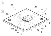
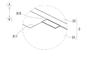
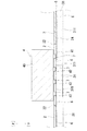
図1〜図3を参照して、実施形態1に係る回路構成体1Aを説明する。回路構成体1Aは、表側回路パターン(図示略)が形成される上面を有する回路基板2と、回路基板2の下面に固定される複数のバスバ3と、バスバ3上に配置される電子部品4とを備える。回路構成体1Aの特徴の一つは、回路基板2が、電子部品4を配置する配置用貫通孔22と、下面から配置用貫通孔22の内側に向かって突出する端子用導体箔24とを備える点にある。以下、詳細を説明する。以下の説明では、説明の便宜上、回路構成体1Aの回路基板2におけるバスバ3側を下、その反対側を上として説明する。
[Circuit structure]
With reference to FIGS. 1-3, the
[回路基板]
回路基板2は、電子部品4が実装される板状部材で、その電子部品4を配置するための配置用貫通孔22を備える(図1〜図3)。回路基板2は、絶縁基板と、絶縁基板の一面(上面)に形成される表側回路パターンとを備える。絶縁基板の他面(下面)には、後述の端子用導体箔24を備える。この下面には、必要に応じて端子用導体箔24に接続される裏側回路パターンがさらに形成されていてもよい。回路基板2は、プリント基板を用いることができる。表側回路パターンは、銅箔で形成されている。絶縁基板の他面(下面)には、バスバ3が固定される。
[Circuit board]
The
(配置用貫通孔)
配置用貫通孔22は、電子部品4をバスバ3上に配置するための孔である。配置用貫通孔22は、隣り合う2つのバスバ31,32に臨むように上下面を貫通している。配置用貫通孔22の輪郭形状は、電子部品4の外形に沿った形状が挙げられ、ここでは矩形状としている。配置用貫通孔22の大きさは、電子部品4を平面視したときの大きさよりも大きい。
(Arrangement through hole)
The placement through
(端子用導体箔)
端子用導体箔24は、電子部品4の端子と電気的かつ機械的に接続される。端子用導体箔24は、その下面から配置用貫通孔22の内側に向かって突出している。即ち、端子用導体箔24は、配置用貫通孔22の一部を覆っている。端子用導体箔24は、絶縁基板の下面のランドにハンダで接合されているのではなく、絶縁基板と絶縁基板の構成材料により一体化されている。そのため、導電材料からなる薄片(リード)を別途用意する必要がなく、薄片を回路基板2の下面のランドにハンダなどで接続する作業を不要にできる。端子用導体箔24の材質は、表側回路パターンと同様、銅が挙げられる。この端子用導体箔24の厚さは、例えば35μm以上400μm以下が挙げられる。端子用導体箔24の厚さが35μm以上であれば、電子部品4の端子を接続する程度の強度を保ち易い。端子用導体箔24の厚さが400μm以下であれば、過度に厚くなり過ぎず、回路基板2全体の厚さも過度に厚くなり過ぎない。端子用導体箔24の厚さは、更に50μm以上300μm以下が好ましく、特に70μm以上200μm以下が好ましい。
(Conductor foil for terminals)
The
[バスバ]
バスバ3は、電力回路を構成する(図1〜図3)。バスバ3は、電源や電気的負荷に接続される。バスバ3の材質は、導電性の金属が挙げられ、具体的には銅や銅合金などが挙げられる。バスバ3の数は複数であり、この複数のバスバ3(31,32)は、回路基板2の他面(下面)に互いに間隔を開けて固定されている(図2)。複数のバスバ3と回路基板2との固定には、これらの間に介在させる粘着シート6(後述)を用いることができる。バスバ31,32の形状は、矩形状である。隣り合う2つのバスバ31,32の上面は、面一である。
[Busba]
The
一方のバスバ31は、そのバスバ31の上面に、端子用導体箔24が嵌め込まれるバスバ凹部を有していてもよい。端子用導体箔24が嵌め込まれるとは、端子用導体箔24の厚み方向の全てがバスバ凹部内に収納されていてもよいし、端子用導体箔24の下面側がバスバ凹部に収納されていて、上面側がバスバ凹部に収納されていなくてもよい。このバスバ凹部は、バスバ31、32の上面(配置用貫通孔22に臨む領域)と端子用導体箔24の上面との段差を緩和する。このバスバ凹部は、回路基板2側からその反対側に窪んだ箇所を形成できればよく、切欠、打ち出し、薄肉化のいずれをも含む。ここでは、バスバ凹部はバスバ切欠部311で構成されている。
One
バスバ切欠部311の大きさは、重複する端子用導体箔24よりも大きくしている(図1〜図3)。バスバ切欠部311は、第1端子41に重複するが第2端子42に重複せず、バスバ切欠部311を形成する内周面が第1端子41と第2端子42との間に位置するように形成されている。バスバ切欠部311の上下方向の形成領域は、一方のバスバ31の上下の全域に亘っている。即ち、バスバ切欠部311は、バスバ31の厚み方向の全域を切り欠いて構成している。
The size of the
[電子部品]
電子部品4は、回路基板2の下面の裏側回路パターン(端子用導体箔24)とバスバ3との両方に実装される(図1〜図3)。電子部品4の種類は、例えば、リレーやFET(Field effect transistor)といったスイッチング素子が挙げられる。
[Electronic parts]
The
電子部品4は、バスバ3上に配置されるパッケージ40と、パッケージ40の下面に配置される端子とを有する。電子部品4がパッケージ40の下面に配置される端子を有することで、端子の長さを短くできる。それにより、端子の電気抵抗を小さくできて低損失化し易い。その上、端子とバスバ3との間の距離を短くできて放熱性を向上し易い。パッケージ40の下面に配置される端子は、下面の輪郭内に配置されていてもよし、輪郭内から輪郭外にはみ出るように配置されていてもよい。パッケージ40の下面に配置される端子の数は、複数とすることができる。パッケージ40の下面に配置される端子の数を複数とする場合、複数の端子の種類は、単一種でもよいし異なる複数種としてもよい。電子部品4は、パッケージ40の下面に配置される端子の他に、下面以外の面(側面)に配置される端子を有していてもよい。
The
ここでは、電子部品4は、パッケージ40の下面に配置される第1端子41、第2端子42、及び第3端子(図示略)の3種類の端子を有する。これら第1端子41と第2端子42と第3端子とは、同一平面上に位置している。この電子部品4は、FETを用いている。図1に示すFETの第1端子41はゲート端子で構成し、その数は1つとしている。第2端子42はソース端子で構成し、その数は3つとしている。第3端子はドレイン端子で構成し、パッケージ40の裏面パターンからなる。1つの第1端子41と3つの第2端子42とはパッケージ40の同一側でパッケージ40に一体に設けられ、第3端子は、パッケージ40の裏面の絶縁材を挟んで第1端子41及び第2端子42の反対側でパッケージ40に一体に設けられている。パッケージ40は、隣り合うバスバ31,32の間隔を跨ぐように配置されている。1つの第1端子41は、端子用導体箔24に電気的かつ機械的に接続されている(図1、図3)。3つの第2端子42は、一方のバスバ31に電気的かつ機械的に接続されている。第3端子は、第2端子42とは異なる他方のバスバ32に電気的かつ機械的に接続されている。
Here, the
これら電気的かつ機械的な接続には、接続金属材料、代表的にはハンダ7(図3)を用いることができる。このハンダ7による接続は、リフロー方式で行うことができる。即ち、電子部品4を端子用導体箔24及び各バスバ31,32に載置する前に、予め所定の位置にハンダペーストを例えば塗布しておく。そして、電子部品4をハンダペーストに載せてから加熱することで電子部品4を端子用導体箔24及び各バスバ31,32に接続する。このように、端子用導体箔24(回路基板2)及びバスバ3と電子部品4との接続をハンダ7のリフローで行えることで、端子用導体箔24及びバスバ3と電子部品4との接続作業性に優れる。この接続に際し、端子用導体箔24の上面とバスバ31,32の上面とが面一で無くても、両上面の段差が僅かであれば、ハンダ7でその段差を吸収できる。
For these electrical and mechanical connections, a connecting metal material, typically solder 7 (FIG. 3) can be used. The connection by the
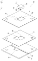
[粘着シート]
粘着シート6は、回路基板2と、複数のバスバ3とを接着する(図1〜図3)。粘着シート6は、両バスバ31,32の上面に両バスバ31,32の間を跨ぐように一連に配置されている。
[Adhesive sheet]
The
粘着シート6には、部品用開口部61が形成されている。部品用開口部61は、電子部品4に重複する箇所に形成されて、電子部品4の各端子と端子用導体箔24及び両バスバ31,32とを電気的かつ機械的に接続できるように設けられている。部品用開口部61の輪郭形状は、電子部品4の外形に沿った形状が挙げられ、ここでは矩形状である。部品用開口部61の大きさは、電子部品4を平面視したときの大きさよりも大きい。
A
粘着シート6には、導体箔用開口部62が形成されていてもよい。そうすれば、両バスバ31,32の上面における配置用貫通孔22に臨む領域と、端子用導体箔24の上面との段差を緩和し易い。特に、バスバ31がバスバ切欠部311(バスバ凹部)を有する場合には、上記段差の緩和に効果的である。導体箔用開口部62は、端子用導体箔24(バスバ切欠部311)に重複する箇所に形成されている。導体箔用開口部62の輪郭形状は、端子用導体箔24の外形に沿った形状が挙げられ、ここでは矩形状である。導体箔用開口部62の大きさは、端子用導体箔24を平面視したときの大きさよりも大きい。この導体箔用開口部62と部品用開口部61とは、互いの角部が重複するように一連に形成されている。
The
粘着シート6の厚さは、例えば、30μm以上150μm以下が挙げられる。粘着シート6の厚さを30μm以上とすれば、回路基板2と複数のバスバ3との接着性及び絶縁性を高め易い。粘着シート6の厚さを150μm以下とすれば、過度に厚くなりすぎず、バスバ31,32の上面と端子用導体箔24の上面との段差を小さくし易い。粘着シート6の厚さは、更に40μm以上100μm以下が好ましい。
As for the thickness of the
粘着シート6の構成材料は、電気絶縁性と電子部品4を実装する際のハンダリフロー温度に対する耐熱性とを有する樹脂が挙げられる。粘着シート6の構成材料は、例えば、高耐熱性アクリル系粘着剤、エポキシ樹脂などの絶縁性接着剤などが挙げられる。
Examples of the constituent material of the pressure-
〔作用効果〕
実施形態1の回路構成体1Aによれば、以下の効果を奏することができる。
[Function and effect]
According to the
(1)電子部品4の回路基板2への実装が容易である。回路基板2が、その下面に配置用貫通孔22に突出する端子用導体箔24を有することで、電子部品4の端子を回路基板2の表側回路パターンに直接接続しなくてもよい。そのため、回路基板2の厚さの分を考慮して端子に曲げ加工を施して曲げる必要がなく、曲げ加工などの作業が不要であるからである。端子を曲げる必要がないため、長さの短い端子を有する電子部品4、例えばパッケージ40の下面に端子を設けたリードレスの電子部品であっても回路基板2へ容易に実装できる。
(1) The
(2)低損失化し易い。上述のように、長さの短い端子を有する電子部品4(リードレスの電子部品)であっても回路基板2へ容易に実装できるため、端子の電気抵抗を小さくできるからである。
(2) It is easy to reduce loss. As described above, even an
(3)放熱性を向上させ易い。上述のように、長さの短い端子を有する電子部品4(リードレスの電子部品)であっても回路基板2へ容易に実装できるため、端子とバスバ3との間の距離を短くできるからである。
(3) It is easy to improve heat dissipation. As described above, even an
(4)生産性に優れる。回路基板2とバスバ3との接着を粘着シート6により行えることで、これらの部材を重ねるだけで一体に固定できるため、組み立て作業性に優れるからである。
(4) Excellent productivity. This is because the
(5)バスバ31,32の上面と端子用導体箔24の上面との段差を小さくし易い。一方のバスバ31は第1端子41が接続される端子用導体箔24を嵌め込むバスバ切欠部311を備えるからである。そのため、電子部品4の傾きを小さくして端子用導体箔24とバスバ31,32に実装できる。
(5) The level difference between the upper surfaces of the bus bars 31 and 32 and the upper surface of the
〔回路基板の製造方法〕
回路基板2の製造は、準備工程と穴あけ加工工程とを備える回路基板の製造方法I、又は準備工程と接着工程と除去工程とを備える回路基板の製造方法IIにより行える。
[Circuit board manufacturing method]
The
[製造方法I]
(準備工程)
準備工程は、導体箔が積層された上下面を有する積層板を準備する。この積層板は、絶縁基板と絶縁基板の上下面の導体箔とを有する。
[Production Method I]
(Preparation process)
The preparation step prepares a laminate having upper and lower surfaces on which conductor foils are laminated. This laminate has an insulating substrate and conductive foils on the upper and lower surfaces of the insulating substrate.
(穴あけ加工工程)
穴あけ加工工程は、積層板に穴あけ加工を施す。この穴あけ加工は、積層板の上下に貫通する貫通孔を形成すると共に、積層板の下面の導体箔の一部で構成され、下面から貫通孔の内側に向かって突出する突出部を形成する。つまり、積層板を貫通する領域と、下面側の導体箔の一部を残して上面側の導体箔と絶縁基板とを除去する領域とを形成する。この貫通孔が配置用貫通孔22を構成し、突出部が端子用導体箔24を構成する。この穴あけ加工は、例えば、機械加工やレーザー加工等が挙げられる。穴あけ加工は、機械加工とレーザー加工とを組み合わせてもよい。組み合わせる場合は、例えば、機械加工で粗加工し、レーザー加工で仕上げ加工することが挙げられる。
(Drilling process)
In the drilling process, the laminated plate is drilled. This drilling process forms a through-hole penetrating up and down the laminated board, and is formed by a part of the conductor foil on the lower surface of the laminated board, and forms a protruding portion that projects from the lower surface toward the inside of the through-hole. That is, a region penetrating the laminated plate and a region where the conductive foil on the upper surface side and the insulating substrate are removed leaving a part of the conductive foil on the lower surface side are formed. This through hole constitutes the arrangement through
[製造方法II]
(準備工程)
準備工程は、導体箔が積層された上面と、上下面に貫通する貫通孔とを有する孔付積層板を準備する。この孔付積層板は、絶縁基板と絶縁基板の上面の導体箔とを有し、絶縁基板の下面には導体箔が設けられていない。
[Production Method II]
(Preparation process)
The preparation step prepares a laminated board with holes having an upper surface on which conductor foils are laminated and through holes penetrating the upper and lower surfaces. This laminated board with holes has an insulating substrate and a conductive foil on the upper surface of the insulating substrate, and no conductive foil is provided on the lower surface of the insulating substrate.
(接着工程)
接着工程は、孔付積層板の下面にその積層板の貫通孔を覆うように導体箔を接着する。導体箔の接着には、例えば、ガラスクロス(ガラス繊維)に樹脂(例えば、エポキシ樹脂など)を含浸させた絶縁性のプリプレグなどの接着シートが利用できる。この接着シートにおける孔付積層板の貫通孔に対応する箇所には、予めその貫通孔と同形状・同サイズの貫通孔を形成しておくとよい。
(Adhesion process)
In the bonding step, the conductor foil is bonded to the lower surface of the laminated board with holes so as to cover the through holes of the laminated board. For bonding the conductor foil, for example, an adhesive sheet such as an insulating prepreg in which a glass cloth (glass fiber) is impregnated with a resin (for example, epoxy resin) can be used. A through hole having the same shape and the same size as the through hole may be formed in advance in a portion corresponding to the through hole of the laminated plate with holes in the adhesive sheet.
(除去工程)
除去工程は、貫通孔を覆う導体箔の一部を溶解して除去する。それにより、孔付積層板の下面からその貫通孔の内側に向かって突出する突出部を形成する。この突出部が、上述の端子用導体箔24を構成する。導体箔の溶解・除去は、例えばエッチングで行える。このとき、残存させたい導体箔の上下面にはマスキングを施す。このマスキングは、上記接着工程で導体箔を孔付積層板に接着する前に予め施しておいてもよい。即ち、所定の位置にマスキングを施した導体箔を孔付積層板に接着してもよい。回路基板2の下面に端子用導体箔24に加えて裏側回路パターンを形成する場合には、この除去工程により端子用導体箔24の形成と裏側回路パターンの形成とを同時に行うことができる。
(Removal process)
In the removing step, a part of the conductor foil covering the through hole is dissolved and removed. Thereby, the protrusion part which protrudes toward the inner side of the through-hole from the lower surface of a laminated board with a hole is formed. This protrusion constitutes the
〔作用効果〕
実施形態1の回路基板の製造方法I・IIによれば、絶縁基板の下面に配置用貫通孔22に突出する端子用導体箔24を有する上述の回路基板2を容易に製造できる。また、端子用導体箔24の位置精度に優れる回路基板2を製造できる。端子用導体箔24は、回路基板2のランドにリードをハンダ付けして形成したものではないため、ハンダ付けの際の位置ずれが生じないからである。
[Function and effect]
According to the circuit board manufacturing methods I and II of the first embodiment, it is possible to easily manufacture the above-described
《実施形態2》
〔回路構成体〕
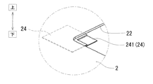
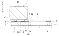
図4,図5を参照して、実施形態2に係る回路構成体を説明する。実施形態2に係る回路構成体は、端子用導体箔24が導体箔凹部241を有する点が実施形態1の回路構成体1Aと相違する。実施形態2に係る回路構成体のその他の点は、実施形態1の回路構成体と同様である。以下、相違点を中心に説明し、同様の構成及び同様の効果については説明を省略する。この点は、以下の実施形態3及び変形例1でも同様である。図4は、端子用導体箔24の拡大図であり、説明の便宜上、一方のバスバ31などのその他の部材を省略して示している。図5は、図3と同様、回路構成体を隣り合う2つのバスバの間を分断する切断線で切断した状態を示す断面図である。
<<
[Circuit structure]
With reference to FIG. 4, FIG. 5, the circuit structure based on
[回路基板]
(端子用導体箔)
端子用導体箔24の導体箔凹部241は、端子用導体箔24の上面とバスバ3(31,32)の上面との上下方向に沿った段差を緩和する。この導体箔凹部241は、端子用導体箔24の上面における電子部品4の第1端子41との接合領域がその下面側に窪むように形成される。即ち、導体箔凹部241は、配置用貫通孔22に臨む領域に形成される。導体箔凹部241の深さ(上下方向に沿った長さ)は、粘着シート6の厚さとすることが挙げられる。それにより、端子用導体箔24の上面と、バスバ3(31,32)の上面とを実質的に面一にし易い。導体箔凹部241の形成は、その上面側から下面側にパンチで打ち出すことで行える。その他、機械加工や、端子用導体箔24をその厚み方向に局所的にエッチングすることでも行える。
[Circuit board]
(Conductor foil for terminals)
The
(その他)
回路基板2の下面には、端子用導体箔24の他、裏側回路パターンを形成することができる。即ち、回路基板2の下面と粘着シート6との間に裏側回路パターンを介在させることができる。その場合、導体箔凹部241の深さを粘着シート6の厚さと裏側回路パターンを構成する導体箔の厚さとの合計厚さとすることが挙げられる。そうすれば、裏側回路パターンが回路基板2の下面と粘着シート6との間に介在されていても、端子用導体箔24の上面と両バスバ31,32の上面とを実質的に面一にすることができる。
(Other)
In addition to the
〔作用効果〕
実施形態2の回路構成体によれば、端子用導体箔24が導体箔凹部241を有することで、端子用導体箔24の上面と両バスバ31,32の上面との段差を小さくできる。特に、導体箔凹部241の深さが粘着シート6の厚さと同じであれば、上記段差を実質的に無くして両上面同士を面一にすることができる。
[Function and effect]
According to the circuit configuration body of the second embodiment, the
《実施形態3》
図6,図7を参照して実施形態3の回路構成体を説明する。実施形態3の回路構成体は、両バスバ31,32がバスバ凸部315を有する点が実施形態1の回路構成体1Aと相違する。各図では、一方のバスバ31のバスバ凸部315のみを図示し、他方のバスバ32のバスバ凸部は図示を省略している。図6は、両バスバ31,32の配置用貫通孔22に臨む箇所(電子部品4の端子が接続される箇所)の拡大図であり、説明の便宜上、端子用導体箔24などのその他の部材を省略して示している。図7は、図3及び図5と同様、回路構成体を隣り合う2つのバスバの間を分断する切断線で切断した状態を示す断面図である。
<<
A circuit configuration of the third embodiment will be described with reference to FIGS. The circuit structure of the third embodiment is different from the
[バスバ]
バスバ3(31,32)のバスバ凸部315は、バスバ3(31,32)の上面と端子用導体箔24の上面との上下方向に沿った段差を緩和する。バスバ凸部315は、バスバ31,32の上面における配置用貫通孔22に臨む領域に上面側に局所的に突出するように形成される。即ち、バスバ31,32の上面における電子部品4の第2端子42と第3端子とのそれぞれの接合領域に形成される。バスバ凸部315の高さ(上下方向に沿った長さ)は、上述の導体箔凹部241と同様、粘着シート6の厚さとすることが挙げられる。それにより、端子用導体箔24の上面と、バスバ3(31,32)の上面とを実質的に面一にし易い。バスバ凸部315の形成は、その下面側から上面側にパンチで打ち出すことや、バスバ3の上面のうち、バスバ凸部315以外の領域を研削して薄肉化することで行える。
[Busba]
The bus bar
[回路基板]
この回路構成体では、実施形態2の回路構成体と同様、回路基板2の下面には、端子用導体箔24の他に裏側回路パターンを形成することができる。その場合、バスバ凸部315の高さは、粘着シート6の厚さと端子用導体箔24の厚さとの合計厚さとすることが挙げられる。そうすれば、実施形態2と同様、裏側回路パターンが回路基板2の下面と粘着シート6との間に介在されていても、端子用導体箔24の上面と両バスバ31,32の上面とを実質的に面一にすることができる。
[Circuit board]
In this circuit configuration body, a back side circuit pattern can be formed on the lower surface of the
〔作用効果〕
実施形態3の回路構成体によれば、両バスバ31,32がバスバ凸部315を有することで、実施形態2と同様、端子用導体箔24の上面と両バスバ31,32の上面との段差を小さくできる。特に、バスバ凸部315の高さを粘着シート6の厚みと同じとすれば、上記段差を実質的に無くして両上面同士を実質的に面一にすることができる。
[Function and effect]
According to the circuit configuration body of the third embodiment, both the bus bars 31 and 32 have the bus bar
《変形例1》
変形例1に係る回路構成体は、図示は省略しているが、一方のバスバのバスバ凹部を切欠ではなく打ち出し又は薄肉化により構成する点が実施形態1の回路構成体1Aと相違する。
<<
Although not shown in the circuit configuration body according to the first modification, the configuration is different from the
[バスバ]
一方のバスバのバスバ凹部は、バスバ切欠部311(図2)と同様、端子用導体箔が嵌め込まれることで、両バスバの上面と端子用導体箔の上面との段差を緩和する。バスバ凹部の大きさは、バスバ切欠部311(図2)と同様、端子用導体箔より大きい。バスバ凹部の深さは、粘着シート6(図2)の厚さとの差以上とすることができる。このバスバ凹部は、一方のバスバを上面側から下面側にパンチで打ち出すことで形成したり、一方のバスバの上面を切削するなどして形成したりすることができる。バスバ凹部を打ち出しにより形成した場合、そのバスバ凹部の下面を構成する箇所には、周辺領域よりも下方に突出する突出部が形成される。一方、バスバ凹部を切削などで形成した場合、そのバスバ凹部の下面を構成する箇所には、周辺領域よりも厚さの薄い薄肉部が形成される。この場合、一方のバスバの下面は、フラットである。薄肉部の厚さは、上記バスバ凹部の深さが粘着シート6の厚さ以上となる程度で、薄肉部の強度が低下しない程度とすることが好ましい。
[Busba]
Similarly to the bus bar notch 311 (FIG. 2), the bus bar recess of one bus bar relaxes the step between the upper surface of both bus bars and the upper surface of the terminal conductor foil by fitting the terminal conductor foil. The size of the bus bar recess is larger than the terminal conductor foil, as is the bus bar notch 311 (FIG. 2). The depth of the bus bar recess can be greater than or equal to the thickness of the adhesive sheet 6 (FIG. 2). The bus bar recess can be formed by punching one bus bar from the upper surface side to the lower surface side, or by cutting the upper surface of one bus bar. When the bus bar recess is formed by punching, a projecting portion that protrudes downward from the peripheral region is formed at a portion constituting the lower surface of the bus bar recess. On the other hand, when the bus bar concave portion is formed by cutting or the like, a thin portion having a thickness smaller than that of the peripheral region is formed at a portion constituting the lower surface of the bus bar concave portion. In this case, the lower surface of one bus bar is flat. It is preferable that the thickness of the thin portion is such that the depth of the bus bar recess is equal to or greater than the thickness of the pressure-
本発明はこれらの例示に限定されるものではなく、特許請求の範囲によって示され、特許請求の範囲と均等の意味および範囲内でのすべての変更が含まれることが意図される。 The present invention is not limited to these exemplifications, but is defined by the scope of the claims, and is intended to include all modifications within the scope and meaning equivalent to the scope of the claims.
本発明の回路基板は、自動車用電気接続箱の内部回路を構成する回路構成体に好適に利用可能である。本発明の回路構成体は、自動車用電気接続箱に好適に利用可能である。本発明の回路構成体は、直流電圧変換装置、AC/DC変換装置、DC/ACインバータなどの大電流パワー回路用基板に好適に利用可能である。本発明の回路基板の製造方法は、上記回路基板の製造に好適に利用可能である。 The circuit board of the present invention can be suitably used for a circuit structure constituting an internal circuit of an electric junction box for automobiles. The circuit structure of the present invention can be suitably used for an electric junction box for automobiles. The circuit structure of the present invention can be suitably used for a substrate for a large current power circuit such as a DC voltage converter, an AC / DC converter, and a DC / AC inverter. The method for manufacturing a circuit board according to the present invention can be suitably used for manufacturing the circuit board.
1A 回路構成体
2 回路基板
22 配置用貫通孔
24 端子用導体箔 241 導体箔凹部
3 バスバ
31 一方のバスバ
311 バスバ切欠部 315 バスバ凸部
32 他方のバスバ
4 電子部品
40 パッケージ 41 第1端子 42 第2端子
6 粘着シート
61 部品用開口部 62 導体箔用開口部
7 ハンダ
DESCRIPTION OF
Claims (7)
前記バスバに臨むように前記上面と前記下面とを貫通して電子部品が配置される配置用貫通孔と、
前記下面から前記配置用貫通孔の内側に向かって突出して前記電子部品の端子が接続される端子用導体箔とを備える回路基板。 A circuit board having an upper surface on which a circuit pattern is formed and a lower surface to which a plurality of bus bars arranged at intervals are fixed,
A placement through hole in which an electronic component is placed through the upper surface and the lower surface so as to face the bus bar;
A circuit board comprising: a terminal conductor foil that protrudes from the lower surface toward the inside of the placement through-hole and to which a terminal of the electronic component is connected.
前記回路基板と接続され、前記回路基板の下面に互いに間隔を開けて固定される複数のバスバと、
前記バスバ上に配置される電子部品とを備え、
前記回路基板は、
前記バスバに臨むように前記上面と前記下面とを貫通して前記電子部品が配置される配置用貫通孔と、
前記下面から前記配置用貫通孔の内側に向かって突出して前記電子部品の端子が接続される端子用導体箔とを有する回路構成体。 A circuit board having an upper surface on which a circuit pattern is formed;
A plurality of bus bars connected to the circuit board and fixed to the lower surface of the circuit board at intervals,
An electronic component disposed on the bus bar,
The circuit board is
A placement through-hole in which the electronic component is placed through the upper surface and the lower surface so as to face the bus bar;
A circuit structure having a terminal conductor foil that protrudes from the lower surface toward the inside of the placement through-hole and to which a terminal of the electronic component is connected.
前記積層板に穴あけ加工を施して前記上下面に貫通する貫通孔を形成する穴あけ加工工程とを備え、
前記穴あけ加工は、前記積層板の下面の前記導体箔の一部を前記貫通孔内に残存させることで、前記下面から前記貫通孔の内側に向かって突出する突出部を形成する回路基板の製造方法。 A preparation step of preparing a laminate having upper and lower surfaces on which conductive foils are laminated;
A drilling process for forming a through hole penetrating the upper and lower surfaces by drilling the laminated plate;
In the drilling process, a part of the conductive foil on the lower surface of the laminated board is left in the through hole, whereby a circuit board is formed that protrudes from the lower surface toward the inside of the through hole. Method.
前記孔付積層板の下面に前記貫通孔を覆うように導体箔を接着する接着工程と、
前記貫通孔を覆う前記導体箔の一部を溶解して除去することで、前記下面から前記貫通孔の内側に向かって突出する突出部を形成する除去工程とを備える回路基板の製造方法。 A preparation step of preparing a laminated board with holes having a top surface on which conductor foils are laminated and through holes penetrating the top and bottom surfaces;
An adhesion step of adhering a conductive foil so as to cover the through hole on the lower surface of the laminated plate with holes;
A circuit board manufacturing method comprising: a removing step of forming a protruding portion protruding from the lower surface toward the inside of the through hole by dissolving and removing a part of the conductor foil covering the through hole.
Priority Applications (5)
| Application Number | Priority Date | Filing Date | Title |
|---|---|---|---|
| JP2016082491A JP6667105B2 (en) | 2016-04-15 | 2016-04-15 | Circuit board, circuit structure, and method of manufacturing circuit board |
| CN201780020125.2A CN108886868B (en) | 2016-04-15 | 2017-04-06 | Circuit board, circuit structure, and manufacturing method of circuit board |
| PCT/JP2017/014405 WO2017179489A1 (en) | 2016-04-15 | 2017-04-06 | Circuit board, circuit constituting member, and circuit board manufacturing method |
| DE112017002029.8T DE112017002029T5 (en) | 2016-04-15 | 2017-04-06 | Printed circuit board, circuit arrangement and production method for a printed circuit board |
| US16/088,207 US10772194B2 (en) | 2016-04-15 | 2017-04-06 | Circuit board, circuit assembly, and circuit board manufacturing method |
Applications Claiming Priority (1)
| Application Number | Priority Date | Filing Date | Title |
|---|---|---|---|
| JP2016082491A JP6667105B2 (en) | 2016-04-15 | 2016-04-15 | Circuit board, circuit structure, and method of manufacturing circuit board |
Publications (2)
| Publication Number | Publication Date |
|---|---|
| JP2017191920A true JP2017191920A (en) | 2017-10-19 |
| JP6667105B2 JP6667105B2 (en) | 2020-03-18 |
Family
ID=60041524
Family Applications (1)
| Application Number | Title | Priority Date | Filing Date |
|---|---|---|---|
| JP2016082491A Active JP6667105B2 (en) | 2016-04-15 | 2016-04-15 | Circuit board, circuit structure, and method of manufacturing circuit board |
Country Status (5)
| Country | Link |
|---|---|
| US (1) | US10772194B2 (en) |
| JP (1) | JP6667105B2 (en) |
| CN (1) | CN108886868B (en) |
| DE (1) | DE112017002029T5 (en) |
| WO (1) | WO2017179489A1 (en) |
Families Citing this family (3)
| Publication number | Priority date | Publication date | Assignee | Title |
|---|---|---|---|---|
| FR3100653B1 (en) * | 2019-09-10 | 2021-07-30 | Valeo Systemes De Controle Moteur | Component forming at least one inductor for an electric circuit |
| JP7419906B2 (en) * | 2020-03-19 | 2024-01-23 | 株式会社オートネットワーク技術研究所 | circuit construct |
| CN113286420A (en) * | 2020-10-28 | 2021-08-20 | 华为技术有限公司 | Circuit bearing plate, power distribution unit and equipment |
Citations (6)
| Publication number | Priority date | Publication date | Assignee | Title |
|---|---|---|---|---|
| JP2000151061A (en) * | 1998-11-05 | 2000-05-30 | Lintec Corp | Electronic circuit, board therefor and manufacture thereof |
| JP2003164039A (en) * | 2001-11-26 | 2003-06-06 | Auto Network Gijutsu Kenkyusho:Kk | Circuit structure and method of manufacturing the same |
| JP2005317908A (en) * | 2004-03-31 | 2005-11-10 | Alps Electric Co Ltd | Board with built-in element and its manufacturing method |
| WO2006073050A1 (en) * | 2005-01-05 | 2006-07-13 | Autonetworks Technologies, Ltd. | Circuit structure |
| JP2010110170A (en) * | 2008-10-31 | 2010-05-13 | Autonetworks Technologies Ltd | Circuit structure body and electric joint box |
| JP2015216754A (en) * | 2014-05-09 | 2015-12-03 | 株式会社オートネットワーク技術研究所 | Circuit structure and electrical connection box |
Family Cites Families (11)
| Publication number | Priority date | Publication date | Assignee | Title |
|---|---|---|---|---|
| JP3540471B2 (en) * | 1995-11-30 | 2004-07-07 | 三菱電機株式会社 | Semiconductor module |
| US6320748B1 (en) * | 2000-03-17 | 2001-11-20 | Celestica International Inc. | Power heatsink for a circuit board |
| DE10254910B4 (en) * | 2001-11-26 | 2008-12-24 | AutoNetworks Technologies, Ltd., Nagoya | Circuit forming unit and method of making the same |
| JP4002427B2 (en) | 2001-11-26 | 2007-10-31 | 株式会社オートネットワーク技術研究所 | Method for manufacturing circuit structure |
| JP4022440B2 (en) * | 2002-07-01 | 2007-12-19 | 株式会社オートネットワーク技術研究所 | Circuit unit |
| JP4148110B2 (en) * | 2003-11-26 | 2008-09-10 | 住友電装株式会社 | Circuit structure |
| JP4584600B2 (en) * | 2004-02-06 | 2010-11-24 | 株式会社オートネットワーク技術研究所 | Circuit structure |
| KR100820633B1 (en) * | 2007-02-15 | 2008-04-11 | 삼성전기주식회사 | Electronic circuit board and manufacturing method |
| WO2012061008A1 (en) * | 2010-10-25 | 2012-05-10 | Hsio Technologies, Llc | High performance electrical circuit structure |
| JP5958768B2 (en) * | 2013-09-24 | 2016-08-02 | 住友電装株式会社 | Circuit structure |
| JP2016082491A (en) | 2014-10-21 | 2016-05-16 | キヤノン株式会社 | Image distribution system and management device of the same |
-
2016
- 2016-04-15 JP JP2016082491A patent/JP6667105B2/en active Active
-
2017
- 2017-04-06 US US16/088,207 patent/US10772194B2/en active Active
- 2017-04-06 WO PCT/JP2017/014405 patent/WO2017179489A1/en not_active Ceased
- 2017-04-06 DE DE112017002029.8T patent/DE112017002029T5/en active Pending
- 2017-04-06 CN CN201780020125.2A patent/CN108886868B/en active Active
Patent Citations (6)
| Publication number | Priority date | Publication date | Assignee | Title |
|---|---|---|---|---|
| JP2000151061A (en) * | 1998-11-05 | 2000-05-30 | Lintec Corp | Electronic circuit, board therefor and manufacture thereof |
| JP2003164039A (en) * | 2001-11-26 | 2003-06-06 | Auto Network Gijutsu Kenkyusho:Kk | Circuit structure and method of manufacturing the same |
| JP2005317908A (en) * | 2004-03-31 | 2005-11-10 | Alps Electric Co Ltd | Board with built-in element and its manufacturing method |
| WO2006073050A1 (en) * | 2005-01-05 | 2006-07-13 | Autonetworks Technologies, Ltd. | Circuit structure |
| JP2010110170A (en) * | 2008-10-31 | 2010-05-13 | Autonetworks Technologies Ltd | Circuit structure body and electric joint box |
| JP2015216754A (en) * | 2014-05-09 | 2015-12-03 | 株式会社オートネットワーク技術研究所 | Circuit structure and electrical connection box |
Also Published As
| Publication number | Publication date |
|---|---|
| WO2017179489A1 (en) | 2017-10-19 |
| CN108886868B (en) | 2021-06-18 |
| US10772194B2 (en) | 2020-09-08 |
| CN108886868A (en) | 2018-11-23 |
| JP6667105B2 (en) | 2020-03-18 |
| US20190289711A1 (en) | 2019-09-19 |
| DE112017002029T5 (en) | 2019-01-24 |
Similar Documents
| Publication | Publication Date | Title |
|---|---|---|
| US9966327B2 (en) | Lead frame, semiconductor device, method for manufacturing lead frame, and method for manufacturing semiconductor device | |
| JP6004001B2 (en) | Semiconductor device | |
| CN107004649B (en) | Heat-dissipating substrates for mounting electronic components | |
| US10576912B2 (en) | Circuit assembly and electrical junction box | |
| WO2015040868A1 (en) | Lead frame, electronic control device using lead frame, and lead-frame mounting method | |
| CN107004648A (en) | Heat dissipation substrate for mounting electronic component | |
| JP2005340639A (en) | Semiconductor device and three-phase inverter device | |
| WO2018123584A1 (en) | Circuit structure and electrical connection box | |
| JP6667105B2 (en) | Circuit board, circuit structure, and method of manufacturing circuit board | |
| WO2017199837A1 (en) | Circuit structure | |
| JP6593597B2 (en) | Circuit structure | |
| JP2004147416A (en) | Circuit body forming method | |
| KR102229077B1 (en) | Connection terminal assembly and circuit board using the connection terminal assembly | |
| JP6028763B2 (en) | Circuit structure and connecting bus bar | |
| JP6065806B2 (en) | Circuit structure and method for manufacturing circuit structure | |
| JP6683018B2 (en) | Heat dissipation board for mounting electronic components | |
| JP6499735B2 (en) | Electronic control unit | |
| JP2017174848A (en) | Wiring board manufacturing method, semiconductor device manufacturing method, and solder plate | |
| JP2016115648A (en) | Bus bar unit, electronic apparatus and method of manufacturing bus bar unit | |
| JP2009253092A (en) | Electronic component | |
| JP2007012839A (en) | Electric circuit unit | |
| JP2014239262A (en) | Electronic equipment and attachment structure of electronic equipment | |
| JP2015065319A (en) | Composite wiring board and method for manufacturing composite wiring board |
Legal Events
| Date | Code | Title | Description |
|---|---|---|---|
| A621 | Written request for application examination |
Free format text: JAPANESE INTERMEDIATE CODE: A621 Effective date: 20180727 |
|
| A131 | Notification of reasons for refusal |
Free format text: JAPANESE INTERMEDIATE CODE: A131 Effective date: 20190902 |
|
| A521 | Request for written amendment filed |
Free format text: JAPANESE INTERMEDIATE CODE: A523 Effective date: 20191015 |
|
| TRDD | Decision of grant or rejection written | ||
| A01 | Written decision to grant a patent or to grant a registration (utility model) |
Free format text: JAPANESE INTERMEDIATE CODE: A01 Effective date: 20200123 |
|
| A61 | First payment of annual fees (during grant procedure) |
Free format text: JAPANESE INTERMEDIATE CODE: A61 Effective date: 20200205 |
|
| R150 | Certificate of patent or registration of utility model |
Ref document number: 6667105 Country of ref document: JP Free format text: JAPANESE INTERMEDIATE CODE: R150 |
|
| R250 | Receipt of annual fees |
Free format text: JAPANESE INTERMEDIATE CODE: R250 |
|
| R250 | Receipt of annual fees |
Free format text: JAPANESE INTERMEDIATE CODE: R250 |