JP2017170627A - Molded product manufacturing method and molded product - Google Patents
Molded product manufacturing method and molded product Download PDFInfo
- Publication number
- JP2017170627A JP2017170627A JP2016055688A JP2016055688A JP2017170627A JP 2017170627 A JP2017170627 A JP 2017170627A JP 2016055688 A JP2016055688 A JP 2016055688A JP 2016055688 A JP2016055688 A JP 2016055688A JP 2017170627 A JP2017170627 A JP 2017170627A
- Authority
- JP
- Japan
- Prior art keywords
- sealing material
- circuit board
- printed circuit
- plate
- sealing
- Prior art date
- Legal status (The legal status is an assumption and is not a legal conclusion. Google has not performed a legal analysis and makes no representation as to the accuracy of the status listed.)
- Withdrawn
Links
- 238000004519 manufacturing process Methods 0.000 title claims abstract description 33
- 239000003566 sealing material Substances 0.000 claims abstract description 89
- 238000007789 sealing Methods 0.000 claims abstract description 47
- 238000002347 injection Methods 0.000 claims abstract description 24
- 239000007924 injection Substances 0.000 claims abstract description 24
- 239000004065 semiconductor Substances 0.000 claims description 107
- 239000000758 substrate Substances 0.000 claims description 44
- 239000000463 material Substances 0.000 claims description 13
- 238000012544 monitoring process Methods 0.000 claims description 8
- 238000007711 solidification Methods 0.000 claims description 5
- 230000008023 solidification Effects 0.000 claims description 5
- 238000005452 bending Methods 0.000 claims description 3
- 239000000243 solution Substances 0.000 abstract 1
- 229920005989 resin Polymers 0.000 description 81
- 239000011347 resin Substances 0.000 description 81
- 238000000034 method Methods 0.000 description 30
- 230000008569 process Effects 0.000 description 11
- 238000000465 moulding Methods 0.000 description 10
- 238000011144 upstream manufacturing Methods 0.000 description 9
- 230000004048 modification Effects 0.000 description 8
- 238000012986 modification Methods 0.000 description 8
- 230000003247 decreasing effect Effects 0.000 description 7
- 238000010586 diagram Methods 0.000 description 7
- 229910052751 metal Inorganic materials 0.000 description 7
- 239000002184 metal Substances 0.000 description 7
- 230000002093 peripheral effect Effects 0.000 description 7
- 229910052802 copper Inorganic materials 0.000 description 5
- 239000010949 copper Substances 0.000 description 5
- 229910000679 solder Inorganic materials 0.000 description 5
- RYGMFSIKBFXOCR-UHFFFAOYSA-N Copper Chemical compound [Cu] RYGMFSIKBFXOCR-UHFFFAOYSA-N 0.000 description 4
- 229910052782 aluminium Inorganic materials 0.000 description 4
- XAGFODPZIPBFFR-UHFFFAOYSA-N aluminium Chemical compound [Al] XAGFODPZIPBFFR-UHFFFAOYSA-N 0.000 description 4
- 239000003822 epoxy resin Substances 0.000 description 4
- 229920000647 polyepoxide Polymers 0.000 description 4
- 230000005540 biological transmission Effects 0.000 description 3
- 239000011248 coating agent Substances 0.000 description 2
- 238000000576 coating method Methods 0.000 description 2
- 230000000052 comparative effect Effects 0.000 description 2
- 239000011521 glass Substances 0.000 description 2
- 229920001721 polyimide Polymers 0.000 description 2
- 230000004044 response Effects 0.000 description 2
- 238000007493 shaping process Methods 0.000 description 2
- 229920001187 thermosetting polymer Polymers 0.000 description 2
- 239000011800 void material Substances 0.000 description 2
- 239000004593 Epoxy Substances 0.000 description 1
- PEEHTFAAVSWFBL-UHFFFAOYSA-N Maleimide Chemical compound O=C1NC(=O)C=C1 PEEHTFAAVSWFBL-UHFFFAOYSA-N 0.000 description 1
- 239000004642 Polyimide Substances 0.000 description 1
- 229910052581 Si3N4 Inorganic materials 0.000 description 1
- XUIMIQQOPSSXEZ-UHFFFAOYSA-N Silicon Chemical compound [Si] XUIMIQQOPSSXEZ-UHFFFAOYSA-N 0.000 description 1
- 239000000654 additive Substances 0.000 description 1
- 230000000996 additive effect Effects 0.000 description 1
- 229920003180 amino resin Polymers 0.000 description 1
- 230000000903 blocking effect Effects 0.000 description 1
- 238000005219 brazing Methods 0.000 description 1
- 239000000919 ceramic Substances 0.000 description 1
- 230000008859 change Effects 0.000 description 1
- PMHQVHHXPFUNSP-UHFFFAOYSA-M copper(1+);methylsulfanylmethane;bromide Chemical compound Br[Cu].CSC PMHQVHHXPFUNSP-UHFFFAOYSA-M 0.000 description 1
- 230000007547 defect Effects 0.000 description 1
- 230000000694 effects Effects 0.000 description 1
- 239000008393 encapsulating agent Substances 0.000 description 1
- 230000005669 field effect Effects 0.000 description 1
- 239000011256 inorganic filler Substances 0.000 description 1
- 229910003475 inorganic filler Inorganic materials 0.000 description 1
- 239000011810 insulating material Substances 0.000 description 1
- 239000012948 isocyanate Substances 0.000 description 1
- 150000002513 isocyanates Chemical class 0.000 description 1
- 230000007246 mechanism Effects 0.000 description 1
- 239000007769 metal material Substances 0.000 description 1
- 229910044991 metal oxide Inorganic materials 0.000 description 1
- 150000004706 metal oxides Chemical class 0.000 description 1
- TWNQGVIAIRXVLR-UHFFFAOYSA-N oxo(oxoalumanyloxy)alumane Chemical compound O=[Al]O[Al]=O TWNQGVIAIRXVLR-UHFFFAOYSA-N 0.000 description 1
- 230000000149 penetrating effect Effects 0.000 description 1
- 239000005011 phenolic resin Substances 0.000 description 1
- 239000004033 plastic Substances 0.000 description 1
- 239000009719 polyimide resin Substances 0.000 description 1
- 239000010703 silicon Substances 0.000 description 1
- 229910052710 silicon Inorganic materials 0.000 description 1
- HQVNEWCFYHHQES-UHFFFAOYSA-N silicon nitride Chemical compound N12[Si]34N5[Si]62N3[Si]51N64 HQVNEWCFYHHQES-UHFFFAOYSA-N 0.000 description 1
- 238000005476 soldering Methods 0.000 description 1
- 238000001721 transfer moulding Methods 0.000 description 1
Images


Classifications
-
- H—ELECTRICITY
- H01—ELECTRIC ELEMENTS
- H01L—SEMICONDUCTOR DEVICES NOT COVERED BY CLASS H10
- H01L23/00—Details of semiconductor or other solid state devices
- H01L23/28—Encapsulations, e.g. encapsulating layers, coatings, e.g. for protection
- H01L23/31—Encapsulations, e.g. encapsulating layers, coatings, e.g. for protection characterised by the arrangement or shape
- H01L23/3107—Encapsulations, e.g. encapsulating layers, coatings, e.g. for protection characterised by the arrangement or shape the device being completely enclosed
- H01L23/3121—Encapsulations, e.g. encapsulating layers, coatings, e.g. for protection characterised by the arrangement or shape the device being completely enclosed a substrate forming part of the encapsulation
-
- B—PERFORMING OPERATIONS; TRANSPORTING
- B29—WORKING OF PLASTICS; WORKING OF SUBSTANCES IN A PLASTIC STATE IN GENERAL
- B29C—SHAPING OR JOINING OF PLASTICS; SHAPING OF MATERIAL IN A PLASTIC STATE, NOT OTHERWISE PROVIDED FOR; AFTER-TREATMENT OF THE SHAPED PRODUCTS, e.g. REPAIRING
- B29C45/00—Injection moulding, i.e. forcing the required volume of moulding material through a nozzle into a closed mould; Apparatus therefor
- B29C45/0046—Details relating to the filling pattern or flow paths or flow characteristics of moulding material in the mould cavity
-
- B—PERFORMING OPERATIONS; TRANSPORTING
- B29—WORKING OF PLASTICS; WORKING OF SUBSTANCES IN A PLASTIC STATE IN GENERAL
- B29C—SHAPING OR JOINING OF PLASTICS; SHAPING OF MATERIAL IN A PLASTIC STATE, NOT OTHERWISE PROVIDED FOR; AFTER-TREATMENT OF THE SHAPED PRODUCTS, e.g. REPAIRING
- B29C45/00—Injection moulding, i.e. forcing the required volume of moulding material through a nozzle into a closed mould; Apparatus therefor
- B29C45/14—Injection moulding, i.e. forcing the required volume of moulding material through a nozzle into a closed mould; Apparatus therefor incorporating preformed parts or layers, e.g. injection moulding around inserts or for coating articles
- B29C45/14065—Positioning or centering articles in the mould
-
- B—PERFORMING OPERATIONS; TRANSPORTING
- B29—WORKING OF PLASTICS; WORKING OF SUBSTANCES IN A PLASTIC STATE IN GENERAL
- B29C—SHAPING OR JOINING OF PLASTICS; SHAPING OF MATERIAL IN A PLASTIC STATE, NOT OTHERWISE PROVIDED FOR; AFTER-TREATMENT OF THE SHAPED PRODUCTS, e.g. REPAIRING
- B29C45/00—Injection moulding, i.e. forcing the required volume of moulding material through a nozzle into a closed mould; Apparatus therefor
- B29C45/14—Injection moulding, i.e. forcing the required volume of moulding material through a nozzle into a closed mould; Apparatus therefor incorporating preformed parts or layers, e.g. injection moulding around inserts or for coating articles
- B29C45/14639—Injection moulding, i.e. forcing the required volume of moulding material through a nozzle into a closed mould; Apparatus therefor incorporating preformed parts or layers, e.g. injection moulding around inserts or for coating articles for obtaining an insulating effect, e.g. for electrical components
- B29C45/14655—Injection moulding, i.e. forcing the required volume of moulding material through a nozzle into a closed mould; Apparatus therefor incorporating preformed parts or layers, e.g. injection moulding around inserts or for coating articles for obtaining an insulating effect, e.g. for electrical components connected to or mounted on a carrier, e.g. lead frame
-
- H—ELECTRICITY
- H01—ELECTRIC ELEMENTS
- H01L—SEMICONDUCTOR DEVICES NOT COVERED BY CLASS H10
- H01L21/00—Processes or apparatus adapted for the manufacture or treatment of semiconductor or solid state devices or of parts thereof
- H01L21/02—Manufacture or treatment of semiconductor devices or of parts thereof
- H01L21/04—Manufacture or treatment of semiconductor devices or of parts thereof the devices having at least one potential-jump barrier or surface barrier, e.g. PN junction, depletion layer or carrier concentration layer
- H01L21/50—Assembly of semiconductor devices using processes or apparatus not provided for in a single one of the subgroups H01L21/06 - H01L21/326, e.g. sealing of a cap to a base of a container
- H01L21/56—Encapsulations, e.g. encapsulation layers, coatings
- H01L21/565—Moulds
-
- H—ELECTRICITY
- H01—ELECTRIC ELEMENTS
- H01L—SEMICONDUCTOR DEVICES NOT COVERED BY CLASS H10
- H01L23/00—Details of semiconductor or other solid state devices
- H01L23/34—Arrangements for cooling, heating, ventilating or temperature compensation ; Temperature sensing arrangements
- H01L23/36—Selection of materials, or shaping, to facilitate cooling or heating, e.g. heatsinks
- H01L23/373—Cooling facilitated by selection of materials for the device or materials for thermal expansion adaptation, e.g. carbon
- H01L23/3735—Laminates or multilayers, e.g. direct bond copper ceramic substrates
-
- H—ELECTRICITY
- H01—ELECTRIC ELEMENTS
- H01L—SEMICONDUCTOR DEVICES NOT COVERED BY CLASS H10
- H01L23/00—Details of semiconductor or other solid state devices
- H01L23/48—Arrangements for conducting electric current to or from the solid state body in operation, e.g. leads, terminal arrangements ; Selection of materials therefor
- H01L23/488—Arrangements for conducting electric current to or from the solid state body in operation, e.g. leads, terminal arrangements ; Selection of materials therefor consisting of soldered or bonded constructions
- H01L23/49—Arrangements for conducting electric current to or from the solid state body in operation, e.g. leads, terminal arrangements ; Selection of materials therefor consisting of soldered or bonded constructions wire-like arrangements or pins or rods
-
- H—ELECTRICITY
- H01—ELECTRIC ELEMENTS
- H01L—SEMICONDUCTOR DEVICES NOT COVERED BY CLASS H10
- H01L23/00—Details of semiconductor or other solid state devices
- H01L23/48—Arrangements for conducting electric current to or from the solid state body in operation, e.g. leads, terminal arrangements ; Selection of materials therefor
- H01L23/488—Arrangements for conducting electric current to or from the solid state body in operation, e.g. leads, terminal arrangements ; Selection of materials therefor consisting of soldered or bonded constructions
- H01L23/498—Leads, i.e. metallisations or lead-frames on insulating substrates, e.g. chip carriers
- H01L23/49811—Additional leads joined to the metallisation on the insulating substrate, e.g. pins, bumps, wires, flat leads
-
- H—ELECTRICITY
- H01—ELECTRIC ELEMENTS
- H01L—SEMICONDUCTOR DEVICES NOT COVERED BY CLASS H10
- H01L23/00—Details of semiconductor or other solid state devices
- H01L23/52—Arrangements for conducting electric current within the device in operation from one component to another, i.e. interconnections, e.g. wires, lead frames
- H01L23/522—Arrangements for conducting electric current within the device in operation from one component to another, i.e. interconnections, e.g. wires, lead frames including external interconnections consisting of a multilayer structure of conductive and insulating layers inseparably formed on the semiconductor body
- H01L23/528—Geometry or layout of the interconnection structure
- H01L23/5283—Cross-sectional geometry
-
- H—ELECTRICITY
- H01—ELECTRIC ELEMENTS
- H01L—SEMICONDUCTOR DEVICES NOT COVERED BY CLASS H10
- H01L23/00—Details of semiconductor or other solid state devices
- H01L23/52—Arrangements for conducting electric current within the device in operation from one component to another, i.e. interconnections, e.g. wires, lead frames
- H01L23/538—Arrangements for conducting electric current within the device in operation from one component to another, i.e. interconnections, e.g. wires, lead frames the interconnection structure between a plurality of semiconductor chips being formed on, or in, insulating substrates
- H01L23/5385—Assembly of a plurality of insulating substrates
-
- B—PERFORMING OPERATIONS; TRANSPORTING
- B29—WORKING OF PLASTICS; WORKING OF SUBSTANCES IN A PLASTIC STATE IN GENERAL
- B29C—SHAPING OR JOINING OF PLASTICS; SHAPING OF MATERIAL IN A PLASTIC STATE, NOT OTHERWISE PROVIDED FOR; AFTER-TREATMENT OF THE SHAPED PRODUCTS, e.g. REPAIRING
- B29C2945/00—Indexing scheme relating to injection moulding, i.e. forcing the required volume of moulding material through a nozzle into a closed mould
- B29C2945/76—Measuring, controlling or regulating
- B29C2945/76003—Measured parameter
- B29C2945/7604—Temperature
-
- B—PERFORMING OPERATIONS; TRANSPORTING
- B29—WORKING OF PLASTICS; WORKING OF SUBSTANCES IN A PLASTIC STATE IN GENERAL
- B29C—SHAPING OR JOINING OF PLASTICS; SHAPING OF MATERIAL IN A PLASTIC STATE, NOT OTHERWISE PROVIDED FOR; AFTER-TREATMENT OF THE SHAPED PRODUCTS, e.g. REPAIRING
- B29C2945/00—Indexing scheme relating to injection moulding, i.e. forcing the required volume of moulding material through a nozzle into a closed mould
- B29C2945/76—Measuring, controlling or regulating
- B29C2945/76177—Location of measurement
- B29C2945/76254—Mould
- B29C2945/76257—Mould cavity
-
- B—PERFORMING OPERATIONS; TRANSPORTING
- B29—WORKING OF PLASTICS; WORKING OF SUBSTANCES IN A PLASTIC STATE IN GENERAL
- B29C—SHAPING OR JOINING OF PLASTICS; SHAPING OF MATERIAL IN A PLASTIC STATE, NOT OTHERWISE PROVIDED FOR; AFTER-TREATMENT OF THE SHAPED PRODUCTS, e.g. REPAIRING
- B29C2945/00—Indexing scheme relating to injection moulding, i.e. forcing the required volume of moulding material through a nozzle into a closed mould
- B29C2945/76—Measuring, controlling or regulating
- B29C2945/76177—Location of measurement
- B29C2945/76287—Moulding material
-
- B—PERFORMING OPERATIONS; TRANSPORTING
- B29—WORKING OF PLASTICS; WORKING OF SUBSTANCES IN A PLASTIC STATE IN GENERAL
- B29C—SHAPING OR JOINING OF PLASTICS; SHAPING OF MATERIAL IN A PLASTIC STATE, NOT OTHERWISE PROVIDED FOR; AFTER-TREATMENT OF THE SHAPED PRODUCTS, e.g. REPAIRING
- B29C2945/00—Indexing scheme relating to injection moulding, i.e. forcing the required volume of moulding material through a nozzle into a closed mould
- B29C2945/76—Measuring, controlling or regulating
- B29C2945/76494—Controlled parameter
- B29C2945/76545—Flow rate
-
- B—PERFORMING OPERATIONS; TRANSPORTING
- B29—WORKING OF PLASTICS; WORKING OF SUBSTANCES IN A PLASTIC STATE IN GENERAL
- B29C—SHAPING OR JOINING OF PLASTICS; SHAPING OF MATERIAL IN A PLASTIC STATE, NOT OTHERWISE PROVIDED FOR; AFTER-TREATMENT OF THE SHAPED PRODUCTS, e.g. REPAIRING
- B29C2945/00—Indexing scheme relating to injection moulding, i.e. forcing the required volume of moulding material through a nozzle into a closed mould
- B29C2945/76—Measuring, controlling or regulating
- B29C2945/76655—Location of control
- B29C2945/76732—Mould
- B29C2945/76735—Mould cavity
-
- B—PERFORMING OPERATIONS; TRANSPORTING
- B29—WORKING OF PLASTICS; WORKING OF SUBSTANCES IN A PLASTIC STATE IN GENERAL
- B29C—SHAPING OR JOINING OF PLASTICS; SHAPING OF MATERIAL IN A PLASTIC STATE, NOT OTHERWISE PROVIDED FOR; AFTER-TREATMENT OF THE SHAPED PRODUCTS, e.g. REPAIRING
- B29C2945/00—Indexing scheme relating to injection moulding, i.e. forcing the required volume of moulding material through a nozzle into a closed mould
- B29C2945/76—Measuring, controlling or regulating
- B29C2945/76655—Location of control
- B29C2945/76765—Moulding material
-
- B—PERFORMING OPERATIONS; TRANSPORTING
- B29—WORKING OF PLASTICS; WORKING OF SUBSTANCES IN A PLASTIC STATE IN GENERAL
- B29K—INDEXING SCHEME ASSOCIATED WITH SUBCLASSES B29B, B29C OR B29D, RELATING TO MOULDING MATERIALS OR TO MATERIALS FOR MOULDS, REINFORCEMENTS, FILLERS OR PREFORMED PARTS, e.g. INSERTS
- B29K2995/00—Properties of moulding materials, reinforcements, fillers, preformed parts or moulds
- B29K2995/0003—Properties of moulding materials, reinforcements, fillers, preformed parts or moulds having particular electrical or magnetic properties, e.g. piezoelectric
- B29K2995/0005—Conductive
-
- B—PERFORMING OPERATIONS; TRANSPORTING
- B29—WORKING OF PLASTICS; WORKING OF SUBSTANCES IN A PLASTIC STATE IN GENERAL
- B29L—INDEXING SCHEME ASSOCIATED WITH SUBCLASS B29C, RELATING TO PARTICULAR ARTICLES
- B29L2031/00—Other particular articles
- B29L2031/34—Electrical apparatus, e.g. sparking plugs or parts thereof
- B29L2031/3406—Components, e.g. resistors
-
- H—ELECTRICITY
- H01—ELECTRIC ELEMENTS
- H01L—SEMICONDUCTOR DEVICES NOT COVERED BY CLASS H10
- H01L2224/00—Indexing scheme for arrangements for connecting or disconnecting semiconductor or solid-state bodies and methods related thereto as covered by H01L24/00
- H01L2224/01—Means for bonding being attached to, or being formed on, the surface to be connected, e.g. chip-to-package, die-attach, "first-level" interconnects; Manufacturing methods related thereto
- H01L2224/10—Bump connectors; Manufacturing methods related thereto
- H01L2224/12—Structure, shape, material or disposition of the bump connectors prior to the connecting process
- H01L2224/13—Structure, shape, material or disposition of the bump connectors prior to the connecting process of an individual bump connector
- H01L2224/13001—Core members of the bump connector
- H01L2224/13075—Plural core members
- H01L2224/1308—Plural core members being stacked
- H01L2224/13083—Three-layer arrangements
-
- H—ELECTRICITY
- H01—ELECTRIC ELEMENTS
- H01L—SEMICONDUCTOR DEVICES NOT COVERED BY CLASS H10
- H01L2224/00—Indexing scheme for arrangements for connecting or disconnecting semiconductor or solid-state bodies and methods related thereto as covered by H01L24/00
- H01L2224/01—Means for bonding being attached to, or being formed on, the surface to be connected, e.g. chip-to-package, die-attach, "first-level" interconnects; Manufacturing methods related thereto
- H01L2224/10—Bump connectors; Manufacturing methods related thereto
- H01L2224/12—Structure, shape, material or disposition of the bump connectors prior to the connecting process
- H01L2224/13—Structure, shape, material or disposition of the bump connectors prior to the connecting process of an individual bump connector
- H01L2224/13001—Core members of the bump connector
- H01L2224/13099—Material
- H01L2224/131—Material with a principal constituent of the material being a metal or a metalloid, e.g. boron [B], silicon [Si], germanium [Ge], arsenic [As], antimony [Sb], tellurium [Te] and polonium [Po], and alloys thereof
-
- H—ELECTRICITY
- H01—ELECTRIC ELEMENTS
- H01L—SEMICONDUCTOR DEVICES NOT COVERED BY CLASS H10
- H01L2224/00—Indexing scheme for arrangements for connecting or disconnecting semiconductor or solid-state bodies and methods related thereto as covered by H01L24/00
- H01L2224/01—Means for bonding being attached to, or being formed on, the surface to be connected, e.g. chip-to-package, die-attach, "first-level" interconnects; Manufacturing methods related thereto
- H01L2224/10—Bump connectors; Manufacturing methods related thereto
- H01L2224/15—Structure, shape, material or disposition of the bump connectors after the connecting process
- H01L2224/16—Structure, shape, material or disposition of the bump connectors after the connecting process of an individual bump connector
- H01L2224/161—Disposition
- H01L2224/16151—Disposition the bump connector connecting between a semiconductor or solid-state body and an item not being a semiconductor or solid-state body, e.g. chip-to-substrate, chip-to-passive
- H01L2224/16221—Disposition the bump connector connecting between a semiconductor or solid-state body and an item not being a semiconductor or solid-state body, e.g. chip-to-substrate, chip-to-passive the body and the item being stacked
- H01L2224/16225—Disposition the bump connector connecting between a semiconductor or solid-state body and an item not being a semiconductor or solid-state body, e.g. chip-to-substrate, chip-to-passive the body and the item being stacked the item being non-metallic, e.g. insulating substrate with or without metallisation
- H01L2224/16227—Disposition the bump connector connecting between a semiconductor or solid-state body and an item not being a semiconductor or solid-state body, e.g. chip-to-substrate, chip-to-passive the body and the item being stacked the item being non-metallic, e.g. insulating substrate with or without metallisation the bump connector connecting to a bond pad of the item
-
- H—ELECTRICITY
- H01—ELECTRIC ELEMENTS
- H01L—SEMICONDUCTOR DEVICES NOT COVERED BY CLASS H10
- H01L2224/00—Indexing scheme for arrangements for connecting or disconnecting semiconductor or solid-state bodies and methods related thereto as covered by H01L24/00
- H01L2224/01—Means for bonding being attached to, or being formed on, the surface to be connected, e.g. chip-to-package, die-attach, "first-level" interconnects; Manufacturing methods related thereto
- H01L2224/26—Layer connectors, e.g. plate connectors, solder or adhesive layers; Manufacturing methods related thereto
- H01L2224/28—Structure, shape, material or disposition of the layer connectors prior to the connecting process
- H01L2224/29—Structure, shape, material or disposition of the layer connectors prior to the connecting process of an individual layer connector
- H01L2224/29001—Core members of the layer connector
- H01L2224/29099—Material
- H01L2224/291—Material with a principal constituent of the material being a metal or a metalloid, e.g. boron [B], silicon [Si], germanium [Ge], arsenic [As], antimony [Sb], tellurium [Te] and polonium [Po], and alloys thereof
-
- H—ELECTRICITY
- H01—ELECTRIC ELEMENTS
- H01L—SEMICONDUCTOR DEVICES NOT COVERED BY CLASS H10
- H01L2224/00—Indexing scheme for arrangements for connecting or disconnecting semiconductor or solid-state bodies and methods related thereto as covered by H01L24/00
- H01L2224/01—Means for bonding being attached to, or being formed on, the surface to be connected, e.g. chip-to-package, die-attach, "first-level" interconnects; Manufacturing methods related thereto
- H01L2224/26—Layer connectors, e.g. plate connectors, solder or adhesive layers; Manufacturing methods related thereto
- H01L2224/31—Structure, shape, material or disposition of the layer connectors after the connecting process
- H01L2224/32—Structure, shape, material or disposition of the layer connectors after the connecting process of an individual layer connector
- H01L2224/321—Disposition
- H01L2224/32151—Disposition the layer connector connecting between a semiconductor or solid-state body and an item not being a semiconductor or solid-state body, e.g. chip-to-substrate, chip-to-passive
- H01L2224/32221—Disposition the layer connector connecting between a semiconductor or solid-state body and an item not being a semiconductor or solid-state body, e.g. chip-to-substrate, chip-to-passive the body and the item being stacked
- H01L2224/32225—Disposition the layer connector connecting between a semiconductor or solid-state body and an item not being a semiconductor or solid-state body, e.g. chip-to-substrate, chip-to-passive the body and the item being stacked the item being non-metallic, e.g. insulating substrate with or without metallisation
- H01L2224/32227—Disposition the layer connector connecting between a semiconductor or solid-state body and an item not being a semiconductor or solid-state body, e.g. chip-to-substrate, chip-to-passive the body and the item being stacked the item being non-metallic, e.g. insulating substrate with or without metallisation the layer connector connecting to a bond pad of the item
-
- H—ELECTRICITY
- H01—ELECTRIC ELEMENTS
- H01L—SEMICONDUCTOR DEVICES NOT COVERED BY CLASS H10
- H01L2224/00—Indexing scheme for arrangements for connecting or disconnecting semiconductor or solid-state bodies and methods related thereto as covered by H01L24/00
- H01L2224/73—Means for bonding being of different types provided for in two or more of groups H01L2224/10, H01L2224/18, H01L2224/26, H01L2224/34, H01L2224/42, H01L2224/50, H01L2224/63, H01L2224/71
- H01L2224/732—Location after the connecting process
- H01L2224/73251—Location after the connecting process on different surfaces
- H01L2224/73253—Bump and layer connectors
-
- H—ELECTRICITY
- H01—ELECTRIC ELEMENTS
- H01L—SEMICONDUCTOR DEVICES NOT COVERED BY CLASS H10
- H01L24/00—Arrangements for connecting or disconnecting semiconductor or solid-state bodies; Methods or apparatus related thereto
- H01L24/01—Means for bonding being attached to, or being formed on, the surface to be connected, e.g. chip-to-package, die-attach, "first-level" interconnects; Manufacturing methods related thereto
- H01L24/10—Bump connectors ; Manufacturing methods related thereto
- H01L24/12—Structure, shape, material or disposition of the bump connectors prior to the connecting process
- H01L24/13—Structure, shape, material or disposition of the bump connectors prior to the connecting process of an individual bump connector
-
- H—ELECTRICITY
- H01—ELECTRIC ELEMENTS
- H01L—SEMICONDUCTOR DEVICES NOT COVERED BY CLASS H10
- H01L24/00—Arrangements for connecting or disconnecting semiconductor or solid-state bodies; Methods or apparatus related thereto
- H01L24/01—Means for bonding being attached to, or being formed on, the surface to be connected, e.g. chip-to-package, die-attach, "first-level" interconnects; Manufacturing methods related thereto
- H01L24/10—Bump connectors ; Manufacturing methods related thereto
- H01L24/15—Structure, shape, material or disposition of the bump connectors after the connecting process
- H01L24/16—Structure, shape, material or disposition of the bump connectors after the connecting process of an individual bump connector
-
- H—ELECTRICITY
- H01—ELECTRIC ELEMENTS
- H01L—SEMICONDUCTOR DEVICES NOT COVERED BY CLASS H10
- H01L24/00—Arrangements for connecting or disconnecting semiconductor or solid-state bodies; Methods or apparatus related thereto
- H01L24/01—Means for bonding being attached to, or being formed on, the surface to be connected, e.g. chip-to-package, die-attach, "first-level" interconnects; Manufacturing methods related thereto
- H01L24/26—Layer connectors, e.g. plate connectors, solder or adhesive layers; Manufacturing methods related thereto
- H01L24/28—Structure, shape, material or disposition of the layer connectors prior to the connecting process
- H01L24/29—Structure, shape, material or disposition of the layer connectors prior to the connecting process of an individual layer connector
-
- H—ELECTRICITY
- H01—ELECTRIC ELEMENTS
- H01L—SEMICONDUCTOR DEVICES NOT COVERED BY CLASS H10
- H01L24/00—Arrangements for connecting or disconnecting semiconductor or solid-state bodies; Methods or apparatus related thereto
- H01L24/01—Means for bonding being attached to, or being formed on, the surface to be connected, e.g. chip-to-package, die-attach, "first-level" interconnects; Manufacturing methods related thereto
- H01L24/26—Layer connectors, e.g. plate connectors, solder or adhesive layers; Manufacturing methods related thereto
- H01L24/31—Structure, shape, material or disposition of the layer connectors after the connecting process
- H01L24/32—Structure, shape, material or disposition of the layer connectors after the connecting process of an individual layer connector
-
- H—ELECTRICITY
- H01—ELECTRIC ELEMENTS
- H01L—SEMICONDUCTOR DEVICES NOT COVERED BY CLASS H10
- H01L2924/00—Indexing scheme for arrangements or methods for connecting or disconnecting semiconductor or solid-state bodies as covered by H01L24/00
- H01L2924/15—Details of package parts other than the semiconductor or other solid state devices to be connected
- H01L2924/181—Encapsulation
Abstract
Description
本発明は、モールド製品の製造方法およびモールド製品に関する。 The present invention relates to a molded product manufacturing method and a molded product.
半導体素子を導電パターン又は導電パターン付きの絶縁基板に搭載して樹脂封止した半導体装置のモールド製品が知られている(特許文献1〜2参照)。また、モールド製品内にボイドが生じてしまうのを防ぐべく、樹脂の流動性を決める部材を、封止される部材に固定する技術(特許文献3〜6参照)、または金型を変形させて樹脂の流動性を変える技術が知られている(特許文献4〜13参照)。
[特許文献1]国際公開第2011−83737号
[特許文献2]特開2014−57005号公報
[特許文献3]特開2008−311558号公報
[特許文献4]特許第3006285号明細書
[特許文献5]特許第5217039号明細書
[特許文献6]特許第5613100号公報
[特許文献7]特開2000−3923号公報
[特許文献8]特開2005−310831号公報
[特許文献9]特開2010−149423号公報
[特許文献10]特開2012−139821号公報
[特許文献11]特開2014−175336号公報
[特許文献12]特開2014−218038号公報
[特許文献13]特許第3784684号明細書
2. Description of the Related Art A mold product of a semiconductor device in which a semiconductor element is mounted on a conductive pattern or an insulating substrate with a conductive pattern and sealed with a resin is known (see
[Patent Document 1] International Publication No. 2011-83737 [Patent Document 2] Japanese Unexamined Patent Application Publication No. 2014-57005 [Patent Document 3] Japanese Unexamined Patent Application Publication No. 2008-31558 [Patent Document 4] Japanese Patent Application Publication No. 30000625 [Patent Document 1] 5] Japanese Patent No. 5217039 [Patent Literature 6] Japanese Patent No. 5613100 [Patent Literature 7] Japanese Patent Laid-Open No. 2000-3923 [Patent Literature 8] Japanese Patent Laid-Open No. 2005-310831 [Patent Literature 9] Japanese Patent Laid-Open No. 2010. [Patent Document 10] JP 2012-139721 [Patent Document 11] JP 2014-175336 [Patent Document 12] JP 2014-218038 [Patent Document 13] Japanese Patent No. 3784684 book
しかし、簡易な構成によって確実にボイドの発生を防止する技術が望まれている。 However, a technique that reliably prevents the generation of voids with a simple configuration is desired.
本発明の第1の態様においては、モールド製品の製造方法であって、モールド製品において封止部分の内部から延伸して外部に露出するべき部分露出部材を、モールド製品における封止部分の内部に封止されるべき封止対象部材に取り付ける取付段階と、部分露出部材が取り付けられた封止対象部材を型に入れて封止材を注入する注入段階と、封止材の注入中における第1期間において、部分露出部材をモールド製品における最終の位置とは異なる位置に保持して部分露出部材に取り付けられた調整部材により封止材の流れを調整する調整段階と、第1期間の後に、封止材を固化させる段階と、を備える製造方法を提供する。 According to a first aspect of the present invention, there is provided a method of manufacturing a molded product, wherein a partially exposed member that is to be exposed from the inside of the sealed portion in the molded product is exposed inside the sealed portion of the molded product. An attachment stage for attaching to a member to be sealed to be sealed, an injection stage for injecting a sealing material by putting the sealing object member to which a partially exposed member is attached into a mold, and a first during injection of the sealing material In the period, an adjustment stage in which the partially exposed member is held at a position different from the final position in the molded product and the flow of the sealing material is adjusted by the adjusting member attached to the partially exposed member; And a step of solidifying the stop material.
本発明の第2の態様においては、封止材と、封止材の内部に封止される封止対象部材と、封止材の内部において封止対象部材に取り付けられ、封止材の内部から延伸して外部に露出する部分露出部材と、を備え、封止対象部材は、部分露出部材に取り付けられた、固化前の封止材の流れを調整するための調整部材を有するモールド製品を提供する。 In the second aspect of the present invention, a sealing material, a sealing target member sealed inside the sealing material, and attached to the sealing target member inside the sealing material, the inside of the sealing material A partially exposed member that is exposed to the outside by extending from the mold, and the sealing target member is a molded product having an adjusting member attached to the partially exposed member for adjusting the flow of the sealing material before solidification. provide.
なお、上記の発明の概要は、本発明の特徴の全てを列挙したものではない。また、これらの特徴群のサブコンビネーションもまた、発明となりうる。 The summary of the invention does not enumerate all the features of the present invention. In addition, a sub-combination of these feature groups can also be an invention.
以下、発明の実施の形態を通じて本発明を説明するが、以下の実施形態は特許請求の範囲にかかる発明を限定するものではない。また、実施形態の中で説明されている特徴の組み合わせの全てが発明の解決手段に必須であるとは限らない。 Hereinafter, the present invention will be described through embodiments of the invention, but the following embodiments do not limit the invention according to the claims. In addition, not all the combinations of features described in the embodiments are essential for the solving means of the invention.
[1.第1実施形態]
[1−1.半導体モジュールの概要]
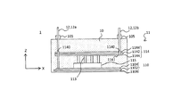
図1Aは、本実施形態に係る半導体モジュール1を示す斜視図である。図1Bは、図1Aの基準線AAに関する半導体モジュール1の断面構成を示す図である。なお、本明細書において、X方向とY方向とは互いに垂直な方向であり、Z方向はX‐Y平面に垂直な方向である。本実施形態の半導体モジュール1は、+Z方向に上面を有し、−Z方向に下面を有する。つまり、「上」および「上方」とは、+Z方向を意味する。これに対して、「下」および「下方」とは、−Z方向を意味する。
[1. First Embodiment]
[1-1. Overview of semiconductor modules]
FIG. 1A is a perspective view showing a
本実施形態においては、モールド製品の一例としての半導体モジュールにおける封止部分の内部から延伸して外部に露出する部分露出部材を、成形中の少なくとも一部の期間に最終位置とは異なる位置に保持することによって封止材の流れを調整し、ボイドの発生を防止する。 In the present embodiment, the partially exposed member that extends from the inside of the sealing portion of the semiconductor module as an example of the molded product and is exposed to the outside is held at a position different from the final position at least during a part of the molding. By adjusting the flow of the sealing material, the generation of voids is prevented.
半導体モジュール1は、モールド製品の一例であり、封止材10、封止材10の内部に封止される1または複数の封止対象部材11、および、外部と電気的に接続するための1または複数のピン12を備える。例えば、本実施形態に係る半導体モジュール1は、制御端子に対する制御入力に応じて主端子間の導通/非導通を切り替えるスイッチング装置である。
The
ここで、スイッチング装置は、固有の閾値電圧を有し、閾値電圧以上のスイッチング電圧を受けて2つのピン12間を通電し、閾値電圧未満のスイッチング電圧を受けて通電を止める。逆に、スイッチング装置は、閾値電圧未満のスイッチング電圧を受けて2つのピン12間を通電し、閾値電圧以上のスイッチング電圧を受けて通電を止めてもよい。スイッチング装置は複数個が並列に接続されて使用されてよい。
Here, the switching device has a unique threshold voltage, energizes between the two
[1−1−1.封止材]
封止材10は、固化した樹脂であってよく、後述の封止対象部材11を封止する。封止材10は、半導体モジュール1の本体部分をなしてよい。例えば、封止材10は、エポキシ樹脂またはマレイミド樹脂等のような絶縁性の熱硬化性樹脂を用いてモールド成形、好ましくはトランスファー成形することで、Y方向を長手とする略直方体状に成形される。封止材10としては、ポリイミド樹脂、イソシアネート樹脂、アミノ樹脂、フェノール樹脂、シリコン系樹脂、又はその他の熱硬化性樹脂を用いてもよい。封止材10は、無機フィラー等の添加物を更に含有してもよい。
[1-1-1. Encapsulant]
The sealing
封止材10のY方向の両端には、上面視において略半円形状の段部101と、段部101をZ方向に貫通する孔部102とが形成されている。孔部102に上方からボルト等の固定具を差し入れることで、半導体モジュール1を外部装置等に固定することができる。
At both ends of the
封止材10の上面の中央には、Y方向に延びる凹部103が形成されてよく、凹部103を挟んでX方向の一側及び他側のそれぞれには、柱状の凸部105がY方向に並設されてよい。凸部105の上面からは、後述のピン12がそれぞれ上方に突出してよい。なお、封止材10の上面に凸部105が設けられずに、当該上面からピン12が上方に突出してもよいし、封止材10の上面に凹部が設けられて、当該凹部からピン12が上方に突出してもよい。
A
[1―1―2.封止対象部材]
本実施形態における1または複数の封止対象部材11は、一例として、1または複数の絶縁基板110と、1または複数の半導体素子115と、1または複数の導通ポスト113と、1または複数のプリント基板114とを有する。
[1-1-2. Member to be sealed]
As an example, the one or more
[1−1−2(1).絶縁基板]
各絶縁基板110は、例えば封止対象部材11の底部に配置されている。一例として、各絶縁基板110はZ方向に対して垂直に配置される。また、本実施形態においては、一例として、複数の絶縁基板110がY方向に並んで設けられている。
[1-1-2 (1). Insulating substrate]
Each insulating
絶縁基板110は、例えばDCB(Direct Copper Bonding)基板、AMB(Active Metal Blazing)基板等である。絶縁基板110には、後述の1または複数のピン12が立設されてよい。各絶縁基板110は、絶縁板1102と、絶縁板1102の上面に形成された1または複数の導電層1104とを有する。各絶縁基板110は、絶縁板1102の下面に形成された伝熱層1108をさらに有してもよい。
The insulating
絶縁板1102は、絶縁性の板状部材であり、例えば窒化アルミニウム、窒化珪素、酸化アルミニウム等の絶縁性セラミックスから構成される板状部材である。絶縁板1102は、樹脂絶縁材料またはガラス材料等から構成される板状部材でもよい。絶縁板1102は、導電層1104および伝熱層1108の間を電気的に絶縁している。
The insulating
導電層1104及び伝熱層1108は、例えば銅、アルミニウム等の導電性金属を用いてそれぞれ形成されている。このうち導電層1104は、半導体素子115に接続する配線パターンを含む。伝熱層1108は、上面の絶縁板1102側からの熱を下面側に逃がす。伝熱層1108の下面は封止材10の底面から露出してよい。
The
[1−1−2(2).半導体素子]
各半導体素子115は、導電層1104上に搭載されている。各半導体素子115は、例えば、パワーMOSFET(金属酸化物半導体電界効果トランジスタ)またはIGBT(絶縁ゲートバイポーラトランジスタ)であってもよいし、FWD(フリーホイールダイオード)であってもよい。また、半導体素子115は、これらが1つのチップ内で縦方向に形成されて表面及び裏面のそれぞれに電極を有するRB−IGBT(逆阻止IGBT)またはRC−IGBT(逆導通IGBT)であってもよい。
[1-1-2 (2). Semiconductor element]
Each
一例として、各半導体素子115は、Si、SiC、GaN等の半導体からなる縦型のスイッチング素子であってよく、表裏面にそれぞれ電極を有してよい。半導体素子115が裏面側に電極を有する場合には、裏面側の電極を半田等の接合材により導電層1104に接続することで半導体素子115が絶縁基板110上に固着されてよい。半導体素子115が表面側に電極を有する場合には、当該表面側の電極には、後述の導通ポスト113が電気的に接続されてよい。
As an example, each
なお、本実施形態に係る半導体モジュール1は3つの半導体素子115を備えているが、1つまたは2つの半導体素子115が備えられてもよいし、4つ以上の半導体素子115が備えられてもよい。複数の半導体素子115は、互いに直列に接続されてもよいし、並列に接続されてもよい。同種の複数の半導体素子115を並列に接続することで、半導体モジュール1において処理可能な定格出力を増やすことができる。また、複数の半導体素子115は、それぞれ別種の素子であってもよい。一例として、複数の115は、互いに並列接続されたIGBTの半導体素子115と、FWDの半導体素子115とを有してもよい。
Although the
[1−1−2(3).導通ポスト]
各導通ポスト113は、それぞれ、半導体素子115と後述のプリント基板114との間に設けられている。導通ポスト113は、半導体素子115およびプリント基板114を熱的および電気的に接続するための部材であり、一例として銅、アルミニウム等、電気抵抗が低く熱伝導率が高い金属を用いて円柱状に成形されている。なお、導通ポスト113は、その下端を半田等の接合材により半導体素子115に接続することで半導体素子115の上に立設され、上端を半田、ロウ付け、又はカシメによりプリント基板114に電気的に接続される。なお、円柱状の導通ポスト113に代えて/加えて、板状のリードフレームやブロック状の導電端子等、他の形状の任意の内部接続部を用いてもよい。
[1-1-2 (3). Continuity post]
Each
[1−1−2(4).プリント基板]
各プリント基板114は、絶縁基板110の上方に絶縁基板110と対向して設けられ、半導体素子115に電気的に接続される。例えば、プリント基板114は、Z方向に対して垂直でよい。また、封止材10による封止部分の上面と、プリント基板114の上面との間の距離は、プリント基板114の下面と絶縁基板110の上面との間の距離よりも大きくてよい。一例として、プリント基板114は、封止材10の上面と、絶縁基板110の上面との間において、絶縁基板110により近い側に配置されてよい。このプリント基板114は、半導体素子115の電極を後述の1または複数のピン12に接続する。
[1-1-2 (4). Printed board]
Each printed circuit board 114 is provided above the insulating
各プリント基板114は、絶縁板1142と、絶縁板1142の表裏面に形成された導電層1144とを有する。絶縁板1142は、例えばガラスエポキシ材等から構成されるリジッド基板又はポリイミド材等から構成されるフレキシブル基板を採用することができる。本実施形態における絶縁板1142は、可撓性を有するフレキシブル基板であってよい。
Each printed board 114 includes an insulating plate 1142 and a
絶縁板1142には、後述のピン12を圧入して通すための孔部1140が設けられている。導電層1144は、銅、アルミニウム等の導電性金属を用いて形成された配線パターンを含む。この配線パターンは、半導体素子115の表面の電極に接続する各導通ポスト113を、対応するピン12に電気的に接続する。
The insulating plate 1142 is provided with a
なお、プリント基板114は、固化前の封止材10の流れを調整するための調整部材として機能する可撓性の板状部材の一例である。例えば、プリント基板114は、プリント基板114の絶縁基板110とは反対側(例えば上面側)における封止材10の流れを調整するように機能してよい。このような機能については、詳細を後述する。
[1−1−3.ピン]
各ピン12は、半導体素子115および/またはプリント基板114と外部との間を電気的に接続するための端子であり、封止材10の内部において封止対象部材11に取り付けられ、封止材10の内部から延伸して外部に露出する。一例として、各ピン12はZ方向と平行に配置されて、X方向における両側部に並列に設けられている。各ピン12は、例えば銅、アルミニウム等の導電性金属を用いて円柱状又は四角柱状に成形されてよい。各ピン12は、板状、ブロック状など、他の形状に形成されてもよい。
The printed circuit board 114 is an example of a flexible plate member that functions as an adjusting member for adjusting the flow of the sealing
[1-1-3. pin]
Each
本実施の形態においては、一例として、複数のピン12は、絶縁基板110の導電層1104に立設された1または複数のピン12aと、プリント基板114に立設された1または複数のピン12bとを有する。
In the present embodiment, as an example, the plurality of
各ピン12aは、絶縁基板110の導電層1104上に立設されて上方に延び、プリント基板114の孔部1140に圧入されて、封止材10の上面の凸部105から突出する。ピン12の下端部は、半田によって導電層1104と熱的および電気的に接続されてよい。一例として、ピン12の下端部は、導電層1104に形成された凹部(図示せず)に圧入されていてもよい。
Each pin 12 a is erected on the
各ピン12aは、導電層1104を介して半導体素子115の電極(例えば裏面側の電極)に接続され、および/または、プリント基板114の導電層1144及び導通ポスト113を介して半導体素子115の表面側の電極に接続されてよい。
Each pin 12a is connected to an electrode (for example, an electrode on the back surface side) of the
各ピン12bは、プリント基板114に立設されて上方に延び、封止材10の上面の凸部105から突出する。ピン12の下面は、半田によって導電層1144と熱的および電気的に接続されてよい。一例として、ピン12bの下端部は、プリント基板114の孔部1140に圧入されてもよいし、導電層1144に形成された凹部(図示せず)に圧入されてもよい。各ピン12bは、プリント基板114の導電層1144及び導通ポスト113を介して半導体素子115の表面側の電極に接続されてよい。
Each pin 12 b is erected on the printed circuit board 114 and extends upward, and protrudes from the
ピン12bの下端部と、孔部1140との接触部分は、例えばエポキシ樹脂などで接着されてもよい。これにより、半導体モジュール1から封止材10が取り除かれた状態でピン12bに対して力が加えられる場合に、絶縁板1142からピン12bが抜けてしまうのを防止することができる。ピン12aの下端部と、孔部1140との接触部分も同様に接着されてよい。
The contact portion between the lower end portion of the pin 12b and the
これらのピン12a、12bを含む複数のピン12は、スイッチング装置としての半導体モジュール1の出力端子、ソース(エミッタ)端子、ドレイン(コレクタ)端子およびゲート(ベース)端子の何れかとして機能してよい。複数のピン12のうちの1または複数には、図示しないインターフェース部材が電気的に接続されてよい。
A plurality of
インターフェース部材は、外部出力端子と、信号配線用のプリント基板と、電力供給配線用のプリント基板とを有してよい。外部出力端子は、出力端子として機能する1または複数のピン12に接続されてよく、半導体モジュール1におけるX方向の側面部に設けられてよい。信号配線用のプリント基板は、ゲート(ベース)端子として機能する1または複数のピン12に電気的に接続されてよい。
The interface member may include an external output terminal, a printed circuit board for signal wiring, and a printed circuit board for power supply wiring. The external output terminal may be connected to one or a plurality of
電力供給配線用のプリント基板は、ドレイン(コレクタ)端子として機能する1または複数のピン12と電源の正電極とを電気的に接続するP側導電板、および、ソース(エミッタ)端子として機能する1または複数のピン12と電源の負電極とを電気的に接続するN側導電板が互いに絶縁されて対向するように積層されたプリント基板を備えてよい。P側導電板およびN側導電板はそれぞれY方向に延伸して半導体モジュール1における全てのピン12を覆ってよく、自身と接続しない1または複数のピン12との対向位置に、当該ピン12を通すための切り欠きを有してよい。
The printed circuit board for power supply wiring functions as a P-side conductive plate that electrically connects one or
ここで、プリント基板114の導電層1144上に立設されてプリント基板114と外部機器とを電気的に接続する1または複数のピン12bは、部分露出部材の一例である。このピン12bは、半導体モジュール1から封止材10が取り除かれた状態で力を加えることにより、プリント基板114を面方向に曲げることができる位置においてプリント基板114に取り付けられている。
Here, the one or more pins 12b that are erected on the
例えば、ピン12bは、成形時にプリント基板114における各位置のうち、封止材10が流れる方向の下流側および/または上流側により近い位置に取り付けられてよい。一例として、ピン12bは、プリント基板114の各位置のうち、成形型内で最も下流側の半導体素子115に対向する位置よりも1cm程度下流側の位置に取り付けられてよい。または、プリント基板114の各位置のうち、導電層1144の配線パターン内で、ピン12bに対する接続部を除き最も下流側の位置よりも1cm程度下流側の位置に取り付けられてよい。
For example, the pin 12b may be attached to a position closer to the downstream side and / or the upstream side in the direction in which the sealing
好ましくは、ピン12bは、プリント基板114の端部1141に取り付けられている。これにより、半導体モジュール1から封止材10が取り除かれた状態、例えば成形前の状態では、ピン12bに対してZ方向に力を加えることでプリント基板114がその法線方向(例えばZ方向)に曲がり、端部1141がZ方向に移動可能となっている。これにより、プリント基板114は固化前の封止材10の流れを調整するための調整部材として機能する。
Preferably, the pin 12b is attached to the
以上の半導体モジュール1によれば、封止対象部材11に含まれるプリント基板114がピン12bに取り付けられ、未硬化の封止材10の流れを調整する。従って、半導体モジュール1を成形する場合に、封止材10の未硬化樹脂の注入中における第1期間で、ピン12bを最終位置とは異なる位置に保持し、プリント基板114により未硬化樹脂の流れを調整することができる。よって、型内の各位置での未硬化樹脂の流速および流入状態を調整することができる。そして、このプリント基板114は、封止後の実動作においては、ピン12bとの間で電気信号を伝送する電気回路として機能する。このようにして、簡易な構成によって確実にボイドの発生を防止することができる。なお、ピン12bの最終位置とは半導体モジュール1内でのピン12bの位置である。ピン12bを最終位置とは異なる位置に保持するとは、例えば、ピン12bを当該位置に固定することであってもよいし、当該位置で揺動させることであってもよい。
According to the
[1−2.半導体モジュールの製造方法]
図2は、本実施形態に係る半導体モジュール1の製造方法を示すフローチャートである。なお、本実施形態においては、一例として、樹脂の注入方向は図1BのX方向であり、注入側に近い側(−X側)が上流側、遠い側(+X側)が下流側である。また、一例として、半導体モジュール1におけるプリント基板114の上部側の断面積よりも、下部側の断面積の方が小さい。但し、上部側の断面積が下部側の断面積よりも小さくてもよい。
[1-2. Manufacturing method of semiconductor module]
FIG. 2 is a flowchart showing a method for manufacturing the
半導体モジュール1を製造するには、まず、封止対象部材11に1または複数のピン12を取り付ける(S102)。例えば、プリント基板114に立設される1または複数のピン12bを、プリント基板114において下流側により近い位置に取り付けてよい。一例として、ピン12bをプリント基板114の孔部1140に圧入して端部1141に取り付けてよい。これにより封止材10が取り除かれた状態の半導体モジュール1が形成されてよい。なお、ピン12bはプリント基板114の上流側の端部、または、上流側および下流側の両方の端部に取り付けてもよい。
To manufacture the
次に、1または複数のピン12が取り付けられた封止対象部材11を型に入れて封止材10の未硬化樹脂の注入を開始する(S104)。例えば、封止材10が取り除かれた状態の半導体モジュール1を成形型に入れてよい。成形型としては、トランスファー成形用の型を用いてよい。
Next, the sealing
封止対象部材11を型内に入れるときには、プリント基板114の上面と型との間の距離がプリント基板114の下面と絶縁基板110の上面との間の距離よりも大きくなるように封止対象部材11を配置してよい。例えば、プリント基板114の上部空間での未硬化樹脂の流路の断面積がプリント基板114の下部空間、つまりプリント基板114と絶縁基板110との間の空間での流路の断面積よりも大きくなるように封止対象部材11を配置してよい。
When the sealing
また、成形型内の各位置のうち、封止材10が流れる方向の下流側により近い位置に、1または複数のピン12bと、プリント基板114の端部1141とを配置してよい。また、成形型から1または複数のピン12bが外部に延伸するように封止対象部材11を配置してよい。また、封止対象部材11が全体として型内で固定されるように、封止対象部材11を配置してよい。
Moreover, you may arrange | position the 1 or several pin 12b and the
封止材10を型内に注入するときには、成形型の各位置のうち、1または複数のピン12bと、プリント基板114とに対してより遠い位置から、封止材10の未硬化樹脂を注入してよい。例えば、注入された未硬化の封止材10が型内を下流側に流れつつ1分程度で固化するように、未硬化樹脂および成形型の温度を設定してよい。一例として、エポキシ樹脂を用いる場合には、成形プロセス中でエポキシ樹脂の硬化反応が進まない約100から180℃の金型に対し、粘度約20Pa・s以下で温度約30から50℃の未硬化樹脂を型内に注入してよい。好ましくは、180℃の金型に、粘度約20Pa・sの未硬化樹脂を型内に注入する。
When the sealing
次に、封止材10の注入中における第1期間において、1または複数のピン12bを半導体モジュール1における最終位置とは異なる1または複数の位置に保持することで、当該ピン12bに取り付けられたプリント基板114によって封止材10の流れを調整する(S106)。
Next, in the first period during the injection of the sealing
ここで、第1期間とは、上述のS104の処理から後述のS108の処理までの間で予め設定されてよい。また、ピン12bの最終位置とは、半導体モジュール1内でのピン12bの位置であり、例えば、プリント基板114が面方向に曲がっていない状態でのピン12bの位置である。なお、半導体モジュール1の特性が許容範囲内である限りにおいて、プリント基板114が曲がった状態でのピン12bの位置を最終位置としてもよい。
Here, the first period may be set in advance from the process of S104 described above to the process of S108 described later. The final position of the pin 12b is the position of the pin 12b in the
このS106では、例えば、ピン12bに力を加えてプリント基板114を面方向に曲げることによりプリント基板114を、未硬化樹脂の流れの調整部材として機能させてよい。また、複数のピン12bに力を加えてプリント基板114をひねることによりプリント基板114を調整部材として機能させてもよい。一例として、ピン12bには、当該ピン12bを押し引きするように正負のZ方向に力を加えてよい。また、ピン12bを倒すように他の方向に力を加えてもよい。 In S <b> 106, for example, the printed circuit board 114 may function as an uncured resin flow adjusting member by bending the printed circuit board 114 in the surface direction by applying a force to the pins 12 b. Alternatively, the printed circuit board 114 may function as an adjustment member by twisting the printed circuit board 114 by applying a force to the plurality of pins 12b. As an example, a force may be applied to the pin 12b in the positive and negative Z directions so as to push and pull the pin 12b. Moreover, you may apply force to another direction so that pin 12b may be fallen.
また、例えば、プリント基板114の上面側における封止材10の流速を調整してよい。一例として、プリント基板114の上部空間での未硬化樹脂の流路の断面積が大きくなる、または、小さくなるようにしてよい。好ましくは、プリント基板114の上面側における未硬化樹脂の流速を制限してよい。例えば、プリント基板114の上流側の端部にピン12bが取り付けられている場合には、ピン12bを上方向に動かすことで、プリント基板114の上面側における未硬化樹脂の流速を制限し、プリント基板114の下部空間に流入する未硬化樹脂の量を増やすことができる。プリント基板114の下流側の端部にピン12bが取り付けられている場合においても、ピン12bを上方向に動かすことで、同様の効果が得られる。
For example, the flow rate of the sealing
ピン12bの保持位置および第1期間の長さとしては、注入開始後の各タイミングで各ピン12bの位置を様々に設定して複数の半導体モジュール1を試作し、ボイドが無い半導体モジュール1が製造された場合での位置および長さを用いてよい。
As the holding position of the pin 12b and the length of the first period, a plurality of
また、例えば、型内における少なくとも1箇所での未硬化樹脂の流速および流入状態の少なくとも一方をモニタリングし、その結果に応じて、1または複数のピン12bの位置を、最終位置とは異なる別の位置にさらに変更してもよい。また、モニタリングの結果に応じて、第1期間を終了してもよい。 Further, for example, at least one of the flow rate and the inflow state of the uncured resin in at least one place in the mold is monitored, and depending on the result, the position of the one or more pins 12b is different from the final position. The position may be further changed. Moreover, you may complete | finish a 1st period according to the result of monitoring.
モニタリングの手法としては、型の1または複数の箇所に1または複数の温度センサ(図示せず)を設けておき、各温度センサが出力する出力信号をモニタリングする手法が挙げられる。温度センサは型の内面から露出して型内の樹脂の温度を直接的に検出してもよいし、型の内部に設けられて型の温度から型内の樹脂の温度を間接的に検出してもよい。この温度センサの出力信号によれば、型内の複数の位置のうち、温度が低下した位置を検出することで、注入された樹脂の到達位置をモニタリングすることができる。また、温度が低下した位置の移動速度を検出することで、未硬化樹脂の流速をモニタリングすることができる。 As a monitoring technique, one or a plurality of temperature sensors (not shown) are provided at one or a plurality of locations on the mold, and an output signal output from each temperature sensor is monitored. The temperature sensor may be exposed from the inner surface of the mold and directly detect the temperature of the resin in the mold, or it is provided inside the mold and indirectly detects the temperature of the resin in the mold from the temperature of the mold. May be. According to the output signal of this temperature sensor, the arrival position of the injected resin can be monitored by detecting the position where the temperature has decreased among the plurality of positions in the mold. Further, the flow rate of the uncured resin can be monitored by detecting the moving speed of the position where the temperature has decreased.
モニタリングの結果に応じて1または複数のピン12bの位置を変更する手法としては、未硬化樹脂の注入口からの距離が同じ温度センサ間で温度差がある場合には、温度が低い方の温度センサの位置で未硬化樹脂の流速を下げるように1または複数のピン12bの位置を変更する手法が挙げられる。また、複数の温度センサの位置に対し、注入開始後の各タイミングにおける温度の目標値を予め設定しておき、目標値より高温の位置では流速を上げ、目標値より低温の位置では流速を下げるように1または複数のピン12bの位置を変更する手法が挙げられる。複数の温度センサの位置での温度の目標値としては、注入開始後の各タイミングで各ピン12bの位置を様々に設定して複数の半導体モジュール1を試作し、ボイドが無い半導体モジュール1が製造された場合での温度プロファイルを用いてよい。
As a method of changing the position of one or a plurality of pins 12b according to the result of monitoring, when there is a temperature difference between temperature sensors having the same distance from the injection port of uncured resin, the lower temperature is used. There is a method of changing the position of one or a plurality of pins 12b so as to reduce the flow rate of the uncured resin at the sensor position. In addition, a target temperature value at each timing after the start of injection is set in advance for a plurality of temperature sensor positions, and the flow rate is increased at a position higher than the target value and decreased at a position lower than the target value. In this way, a method of changing the position of one or a plurality of pins 12b can be mentioned. As a target temperature value at the positions of a plurality of temperature sensors, a plurality of
モニタリングの結果に応じて第1期間を終了する手法としては、未硬化樹脂の注入口からの距離が同じ下流側の温度センサ間で温度の変化タイミングに差がない場合、つまり未硬化樹脂の到達タイミングが同じであると推定される場合に第1期間を終了する手法が挙げられる。 As a method of ending the first period according to the result of monitoring, there is no difference in temperature change timing between temperature sensors on the downstream side having the same distance from the injection port of the uncured resin, that is, the arrival of the uncured resin. A method of ending the first period when the timing is estimated to be the same is given.
次に、1または複数のピン12bを半導体モジュール1における最終位置に配置する(S108)。例えば、プリント基板114を曲がっていない状態に戻す。ピン12bに力を加えてピン12bを最終位置に配置してもよい。このS108の処理は、未硬化樹脂の注入完了の直前に行ってもよい。なお、S108の処理を行わずに、S106でのピン12bに対する保持を解除して、樹脂の圧力によってピン12bおよびプリント基板114を最終位置に配置させてもよい。 Next, one or more pins 12b are arranged at the final position in the semiconductor module 1 (S108). For example, the printed circuit board 114 is returned to an unbent state. A force may be applied to the pin 12b to place the pin 12b in the final position. The process of S108 may be performed immediately before the completion of the injection of the uncured resin. Instead of performing the process of S108, the holding of the pin 12b in S106 may be released, and the pin 12b and the printed board 114 may be arranged at the final position by the pressure of the resin.
そして、注入を完了して型内の未硬化樹脂を固化させる(S110)。これにより、半導体モジュール1が製造される。
Then, the injection is completed and the uncured resin in the mold is solidified (S110). Thereby, the
以上の製造方法によれば、封止材10の未硬化樹脂の注入中における第1期間で、ピン12bを最終位置とは異なる位置に保持してプリント基板114により未硬化樹脂の流れを調整した後に、ピン12bを最終位置に配置するので、型内の各位置での未硬化樹脂の流速および流入状態を調整することができる。従って、金型への可動機構の追加等なく、簡易な構成によって確実にボイドの発生を防止することができる。
According to the above manufacturing method, in the first period during the injection of the uncured resin of the sealing
[1−3.ピンの位置と未硬化樹脂の流速との関係]
図3A〜図3Cは、封止材10の未硬化樹脂が型1000に注入されているときの、ピン12bの位置と未硬化樹脂の流速との関係を示す図である。より具体的には、図3Aは、第1期間においてピン12bを最終位置に保持したとき(例えばピン12bに力を加えないとき)の未硬化樹脂の流速を示す図である。図3Bは、第1期間においてピン12bを最終位置よりも上の位置に保持したときの未硬化樹脂の流速を示す図である。図3Cは、第1期間においてピン12bを最終位置よりも上の位置に保持したときの未硬化樹脂の流速を示す図である。なお、図3A〜図3Cでは、段部101、孔部102、凹部103および凸部105を成形するための型部分の図示を省略している。
[1-3. Relationship between pin position and uncured resin flow velocity]
3A to 3C are diagrams showing the relationship between the position of the pin 12b and the flow rate of the uncured resin when the uncured resin of the sealing
図3Aに示すように、第1期間においてピン12bを最終位置に保持したときには、プリント基板114の上部空間での未硬化樹脂の流速の方が、プリント基板114の下部空間での未硬化樹脂の流速よりも大きくなる(網掛けの矢印参照)。そのため、下部空間を流れる未硬化樹脂と、上部空間を流れて型1000の下流側の端部から下部空間に回り込む未硬化樹脂とが、下部空間に位置する下流側の半導体素子115の近傍で合流してウェルドラインを形成する。ウェルドラインには、ボイドなどの欠点が含まれやすい。
As shown in FIG. 3A, when the pin 12b is held at the final position in the first period, the flow rate of the uncured resin in the upper space of the printed circuit board 114 is higher than that of the uncured resin in the lower space of the printed circuit board 114. It is larger than the flow rate (see shaded arrows). Therefore, the uncured resin that flows in the lower space and the uncured resin that flows in the upper space and flows into the lower space from the downstream end of the
このようにして製造された半導体モジュールは本実施形態に係る半導体モジュール1の比較例である。この半導体モジュールでは、エックス線透過観察法によって観察を行うと、半導体素子115の周囲にボイドが約50%発生していた。
The semiconductor module manufactured in this way is a comparative example of the
また、図3Bに示すように、第1期間においてピン12bを最終位置よりも上の位置に保持したときには、プリント基板114の上部空間での未硬化樹脂の流速と、プリント基板114の下部空間での未硬化樹脂の流速とが同程度となる(網掛けの矢印参照)。そのため、下部空間を流れる未硬化樹脂と、上部空間を流れる未硬化樹脂とが、封止対象部材11よりも型1000の下流側で合流してウェルドラインを形成する。
3B, when the pin 12b is held at a position higher than the final position in the first period, the flow rate of the uncured resin in the upper space of the printed circuit board 114 and the lower space of the printed circuit board 114 The flow rate of the uncured resin is approximately the same (see shaded arrows). Therefore, the uncured resin flowing in the lower space and the uncured resin flowing in the upper space merge on the downstream side of the
このようにして製造された半導体モジュールは、本実施形態に係る半導体モジュール1の実施例である。この半導体モジュール1では、エックス線透過観察法によって観察を行うと、半導体モジュール1内にボイドが0%発生していた。
The semiconductor module manufactured in this way is an example of the
また、図3Cに示すように、第1期間においてピン12bを最終位置よりも下の位置に保持したときには、プリント基板114の上部空間での未硬化樹脂の流速の方が、プリント基板114の下部空間での未硬化樹脂の流速よりも著しく大きくなる(網掛けの矢印参照)。そのため、下部空間を流れる未硬化樹脂と、上部空間を流れて型1000の下流側の端部から下部空間に回り込む未硬化樹脂とが、下部空間に位置する半導体素子115等の近傍で合流してウェルドラインを形成する。
Further, as shown in FIG. 3C, when the pin 12b is held at a position lower than the final position in the first period, the flow rate of the uncured resin in the upper space of the printed circuit board 114 is lower than the printed circuit board 114. Significantly greater than the flow rate of uncured resin in space (see shaded arrows). Therefore, the uncured resin that flows in the lower space and the uncured resin that flows in the upper space and flows from the downstream end of the
このようにして製造された半導体モジュールは、本実施形態に係る半導体モジュール1の比較例としてもよい。この半導体モジュールでは、エックス線透過観察法によって観察を行うと、プリント基板114の下部および半導体素子115の周囲にボイドが100%発生していた。
The semiconductor module manufactured as described above may be a comparative example of the
[2.第2実施形態]
[2−1.半導体モジュールの概要]
図4は、図1Aの基準線BBに関する半導体モジュール1Aの断面構成を示す図である。この図に示すように、本実施形態に係る半導体モジュール1Aは、ピン12の少なくとも一部として1または複数のピン12cを、封止対象部材11の代わりに1または複数の封止対象部材11Aを備えている。半導体モジュール1Aは、第1実施形態における1または複数のピン12bと、1または複数のピン12cとを備えてもよい。
[2. Second Embodiment]
[2-1. Overview of semiconductor modules]
FIG. 4 is a diagram illustrating a cross-sectional configuration of the
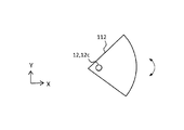
1または複数のピン12cは、棒状部材の一例である。このピン12cは、円柱状となっており、封止材10が取り除かれた状態で、板状部材の一例としての絶縁基板110および/またはプリント基板114に対し、電気的に接続され、かつ回転可能に取り付けられる。
The one or more pins 12c are an example of a rod-shaped member. The pin 12c has a cylindrical shape, and is electrically connected to an insulating
例えば、ピン12cの下端部は、絶縁基板110の導電層1104に形成された凹部(図示せず)またはプリント基板114の孔部1140に圧入されている。また、ピン12cの側周面のうち、少なくとも絶縁板1142との当接領域と、孔部1140の内周面とのうち少なくとも一方には、絶縁板1142よりも靱性に優れた材料によってコーディングが行われてよい。これにより、半導体モジュール1から封止材10が取り除かれた状態でピン12cが絶縁板1142に対して回転する場合に、絶縁板1142が破損してしまうのを防止することができる。
For example, the lower end of the pin 12 c is press-fitted into a recess (not shown) formed in the
例えば、ピン12cの側周面にコーティングが行われる場合には、導電性で、かつ、熱伝導率が高い材料でコーティングされてよい。一例として、ピン12cの側周面には、ピン12cと同種の金属によりメッキが施されてよいし、ピン12cとは異なる金属(例えば半田)によるメッキが施されてもよい。 For example, when the coating is performed on the side peripheral surface of the pin 12c, the pin 12c may be coated with a material that is conductive and has high thermal conductivity. As an example, the side peripheral surface of the pin 12c may be plated with the same type of metal as the pin 12c, or may be plated with a metal (for example, solder) different from the pin 12c.
また、孔部1140の内周面にコーティングが行われる場合には、絶縁性で、かつ、熱伝導率が高い材料でコーティングされてよい。一例として、孔部1140の内周面には、樹脂によってコーティングが施されてよい。
Further, when coating is performed on the inner peripheral surface of the
1または複数の封止対象部材11Aは、1または複数のピン12cに取り付けられた、固化前の封止材10の流れを調整するための1または複数の調整部材112を有する。調整部材112は、半導体モジュール1から封止材10が取り除かれた状態において、ピン12cの軸回転に応じて回転可能であってよい。調整部材112は、プリント基板114の絶縁基板110とは反対側(例えば上面側)における封止材10の流れを調整するように機能してよい。一例として、調整部材112は、プリント基板114よりも上方に位置してよく、プリント基板114の近くに位置することが好ましい。
One or more
なお、各ピン12cに対して1つの調整部材112が取り付けられてもよいし、複数の調整部材112が取り付けられてもよい。また、複数のピン12cのうち、何れかのピン12cのみに調整部材112が取り付けられてもよい。
One
図5は、調整部材112を示す斜視図である。調整部材112は、ピン12cの回転に伴って向きが変わる板状であってよい。例えば、調整部材112は、Z方向と垂直な断面形状が、回転中心を通る直線の方向によって長さが異なる形状であってよく、一例として、端部に回転中心が設けられた楕円形状となっている。なお、封止材10の未硬化樹脂が固化した後の応力集中を避ける観点からは、調整部材112は、角部が面取りされていることが好ましい。
FIG. 5 is a perspective view showing the
また、調整部材112は、成形時に封止材10の未硬化樹脂を一部通すための少なくとも1つの開孔1120を側周面に有してよい。例えば、開孔1120は、調整部材112が未硬化樹脂の流れ方向に対して直交または略直交するときに未硬化樹脂を通してよい。この場合には、調整部材112に対して下流側に隣接する領域に樹脂を流すことができるため、ボイドの発生を防止することができる。
Further, the
また、調整部材112は、ピン12cと一体に形成されてよい。例えば、調整部材112は、ピン12cの金属材料によってピン12cと一体成形されてよい。
The
また、調整部材112は、封止材10と同一材料により形成されてもよい。例えば、調整部材112は、ピン12cを型内に配置して封止材10と同一材料で調整部材112を成形するインサート成形法を用いて形成されてもよい。
The
[2−2.半導体モジュールの製造方法]
半導体モジュール1Aは、図2に関連して示した上述の半導体モジュール1と同様の製造方法によって製造される。
[2-2. Manufacturing method of semiconductor module]
The
但し、半導体モジュール1Aを製造するには、S102の処理において、封止対象部材11Aにおける絶縁基板110および/またはプリント基板114に対して1または複数のピン12cを回転可能に取り付ける。ピン12cは未硬化樹脂の流れに対する下流側に設けられてもよいし、上流側に設けられてもよいし、上流側および下流側にそれぞれ設けられてもよい。絶縁基板110および/またはプリント基板114に対して、回転不能な1または複数のピン12をさらに取り付けてもよい。
However, in order to manufacture the
また、封止部分において調整部材112が位置する深さが複数のピン12cの間で互いに異なるように、各調整部材112を配置してよい。例えば、封止材10の未硬化樹脂が流れる方向の上流側ほど調整部材112の位置を高くし、下流側ほど調整部材112の位置を低くしてプリント基板114の近くに配置してよい。逆に、上流側ほど調整部材112の位置を低くしてプリント基板114の近くに配置し、下流側ほど調整部材112の位置を高くしてもよい。
Moreover, you may arrange | position each
所望の深さに配置される調整部材112が設けられたピン12cを用意するには、例えば、予め同形状の複数のピン12cの異なる位置にそれぞれ調整部材112を設けておき、所望の位置に調整部材112が設けられたピン12cを選択してもよい。また、長尺なピン12cの中途部に調整部材112を設けておき、ピン12cの両端をカットすることで、所望の位置に調整部材112が設けられたピン12cを形成してもよい。また、ピン12cに対して調整部材112を摺動可能に設けておき、調整部材112を所望の位置に移動させてもよい。
In order to prepare the pin 12c provided with the
また、S106の処理では、封止材10の注入中における第1期間において、各ピン12cを回転方向における最終回転位置とは異なる回転位置で保持してよい。これにより、調整部材112が最終回転位置とは異なる回転位置で保持される結果、封止材10の流れが調整される。
In the process of S106, each pin 12c may be held at a rotation position different from the final rotation position in the rotation direction in the first period during the injection of the sealing
ここで、ピン12cの最終の回転位置とは、例えば半導体モジュール1内でのピン12cの回転位置であり、一例として、調整部材112が未硬化樹脂の流れ方向に沿った状態でのピン12cの回転位置である。ピン12cを最終の回転位置とは異なる回転位置に保持するとは、例えば、ピン12cを当該回転位置に固定することであってもよいし、当該回転位置で揺動させることであってもよい。
Here, the final rotational position of the pin 12c is, for example, the rotational position of the pin 12c in the
このS106では、例えば、プリント基板114の上面側における封止材10の流速を調整してよい。一例として、プリント基板114の上部空間での未硬化樹脂の流路の断面積が大きくなる、または、小さくなるようにしてよい。好ましくは、プリント基板114の上面側における未硬化樹脂の流速を制限してよい。
In S106, for example, the flow rate of the sealing
ピン12cの保持される回転位置および第1期間の長さとしては、注入開始後の各タイミングで各ピン12cの回転位置を様々に設定して複数の半導体モジュール1を試作し、ボイドが無い半導体モジュール1が製造された場合での回転位置および長さを用いてよい。
As the rotational position where the pin 12c is held and the length of the first period, a plurality of
また、例えば、型内における少なくとも1箇所での未硬化樹脂の流速および流入状態の少なくとも一方を第1実施形態と同様にモニタリングし、その結果に応じて、1または複数のピン12cの回転位置を、最終回転位置とは異なる別の位置にさらに変更してもよい。また、モニタリングの結果に応じて、第1期間を終了してもよい。 Further, for example, at least one of the flow rate and the inflow state of the uncured resin in at least one place in the mold is monitored in the same manner as in the first embodiment, and the rotational position of one or a plurality of pins 12c is determined according to the result. The position may be further changed to a position different from the final rotation position. Moreover, you may complete | finish a 1st period according to the result of monitoring.
モニタリングの結果に応じて1または複数のピン12cの回転位置を変更する手法としては、未硬化樹脂の注入口からの距離が同じ温度センサ間で温度差がある場合に、温度が低い方の温度センサの位置で未硬化樹脂の流速を下げるように1または複数のピン12cの回転位置を変更する手法が挙げられる。また、複数の温度センサの位置に対し、注入開始後の各タイミングにおける温度の目標値を予め設定しておき、目標値より高温の位置では流速を上げ、目標値より低温の位置では流速を下げるように1または複数のピン12cの回転位置を変更する手法が挙げられる。複数の温度センサの位置での温度の目標値としては、注入開始後の各タイミングで各ピン12cの回転位置を様々に設定して複数の半導体モジュール1を試作し、ボイドが無い半導体モジュール1が製造された場合での温度プロファイルを用いてよい。
As a method of changing the rotational position of one or a plurality of pins 12c according to the result of monitoring, when there is a temperature difference between temperature sensors having the same distance from the uncured resin injection port, the lower temperature There is a method of changing the rotational position of one or a plurality of pins 12c so as to reduce the flow rate of the uncured resin at the sensor position. In addition, a target temperature value at each timing after the start of injection is set in advance for a plurality of temperature sensor positions, and the flow rate is increased at a position higher than the target value and decreased at a position lower than the target value. As described above, there is a method of changing the rotational position of one or a plurality of pins 12c. As a target temperature value at the positions of the plurality of temperature sensors, a plurality of
また、S108の処理では、ピン12cを最終の回転位置に回転させてよい。ピン12cに力を加えてピン12cを最終の回転位置に配置してもよいし、S106でのピン12cに対する保持を解除することでピン12cを最終の回転位置に配置してもよい。 In the process of S108, the pin 12c may be rotated to the final rotation position. A force may be applied to the pin 12c to place the pin 12c in the final rotational position, or the pin 12c may be placed in the final rotational position by releasing the holding of the pin 12c in S106.
以上の製造方法によっても、型内の各位置での未硬化樹脂の流速および流入状態を調整することができるため、簡易な構成によって確実にボイドの発生を防止することができる。 Also by the above manufacturing method, since the flow rate and inflow state of the uncured resin at each position in the mold can be adjusted, generation of voids can be reliably prevented with a simple configuration.
[2−3.調整部材の変形例]
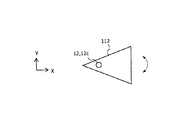
図6A〜図6Dは、変形例における調整部材112の断面形状を示す図である。この図に示すように、調整部材112のZ方向と垂直な断面形状は、回転中心を通る直線の方向によって長さが異なる限りにおいて、多様な形状とすることができる。
[2-3. Modification of adjustment member]
6A to 6D are diagrams illustrating a cross-sectional shape of the
例えば、調整部材112のZ方向と垂直な断面形状は、図6Aに示すように、部分円状であってもよいし、図6B、図6Cに示すように、3角形などの多角形状であってもよい。ここで、調整部材112の回転中心は、図6A、図6Bに示すように、中心から外れた位置にあってもよいし、図6Cに示すように、断面形状の中心位置にあってもよい。回転中心が断面形状の中心から外れた位置にある場合には、未硬化樹脂の流れの調整度合いが大きくなる。
For example, the cross-sectional shape perpendicular to the Z direction of the
また、調整部材112の断面形状は、図6A、図6Bに示すように、回転中心から離れるに従って幅が広くなってよい。この場合には、調整部材112の側面のうち、長尺な側面を未硬化樹脂の流れに対向させて流れを制限するときに、当該側面よりも下流側の空間が調整部材112自体で充填された状態となる。例えば、回転中心からの距離によらず幅が一定の板状の調整部材112では、その長尺な側面を流れに対向させると、調整部材112よりも下流側に、樹脂が流れ込みにくい領域が生じる。これに対し、例えば図6Bに示す調整部材112では、このように樹脂が流れ込みにくい領域が、調整部材112自体によって満たされる。そのため、調整部材112の下流側にボイドが生じるのが防止される。
Further, as shown in FIGS. 6A and 6B, the cross-sectional shape of the
また、調整部材112のZ方向と垂直な断面形状は、図6Dに示すように、部分円状および多角形とは異なる任意の形状としてもよい。また、調整部材112の断面形状は、回転中心を通る如何なる直線に対しても非対称であってよい。
Further, the cross-sectional shape perpendicular to the Z direction of the
[3.第1、第2実施形態の変形例]
上記第1、第2の実施形態では、モールド製品を半導体モジュール1として説明したが、例えば半導体素子を含まないモールド製品、電気回路を含まないモールド製品、端子等がインサート成形された製品(樹脂ケース等)、プラモデル製品など、任意のモールド製品としてよい。
[3. Modification of First and Second Embodiments]
In the first and second embodiments, the molded product has been described as the
また、封止対象部材11に取り付けられ外部に露出する部分露出部材を、半導体素子115および/またはプリント基板114と外部機器とを電気的に接続するピン12bとして説明したが、他の機能を有する部材としてもよい。
Further, the partially exposed member that is attached to the sealing
また、上記第1の実施形態では、調整部材をプリント基板114として説明したが、これに加えて/代えて、封止材10が取り除かれた状態でピン12に力を加えることで上下に曲がる可撓性の板状部材を調整部材としてもよい。このような板状部材は、絶縁基板110であってもよいし、プリント基板114に貼り付けられてピン12が立設された他の板状部材としてもよい。
In the first embodiment, the adjustment member has been described as the printed circuit board 114. In addition, instead of this, the bending member is bent up and down by applying a force to the
以上、本発明を実施の形態を用いて説明したが、本発明の技術的範囲は上記実施の形態に記載の範囲には限定されない。上記実施の形態に、多様な変更または改良を加えることが可能であることが当業者に明らかである。その様な変更または改良を加えた形態も本発明の技術的範囲に含まれ得ることが、特許請求の範囲の記載から明らかである。 As mentioned above, although this invention was demonstrated using embodiment, the technical scope of this invention is not limited to the range as described in the said embodiment. It will be apparent to those skilled in the art that various modifications or improvements can be added to the above-described embodiment. It is apparent from the scope of the claims that the embodiments added with such changes or improvements can be included in the technical scope of the present invention.
特許請求の範囲、明細書、および図面中において示した装置、システム、プログラム、および方法における動作、手順、ステップ、および段階等の各処理の実行順序は、特段「より前に」、「先立って」等と明示しておらず、また、前の処理の出力を後の処理で用いるのでない限り、任意の順序で実現しうることに留意すべきである。特許請求の範囲、明細書、および図面中の動作フローに関して、便宜上「まず、」、「次に、」等を用いて説明したとしても、この順で実施することが必須であることを意味するものではない。 The order of execution of each process such as operations, procedures, steps, and stages in the apparatus, system, program, and method shown in the claims, the description, and the drawings is particularly “before” or “prior to”. It should be noted that the output can be realized in any order unless the output of the previous process is used in the subsequent process. Regarding the operation flow in the claims, the description, and the drawings, even if it is described using “first”, “next”, etc. for convenience, it means that it is essential to carry out in this order. It is not a thing.
1 半導体モジュール、1A 半導体モジュール、10 封止材、11 封止対象部材、11A 封止対象部材、12 ピン、12a ピン、12b ピン、12c ピン、101 段部、102 孔部、103 凹部、105 凸部、110 絶縁基板、112 調整部材、113 導通ポスト、114 プリント基板、115 半導体素子、1000 型、1102 絶縁板、1104 導電層、1108 伝熱層、1120 開孔、1140 孔部、1141 端部、1142 絶縁板、1144 導電層
DESCRIPTION OF
Claims (28)
前記モールド製品において封止部分の内部から延伸して外部に露出するべき部分露出部材を、前記モールド製品における封止部分の内部に封止されるべき封止対象部材に取り付ける取付段階と、
前記部分露出部材が取り付けられた前記封止対象部材を型に入れて封止材を注入する注入段階と、
前記封止材の注入中における第1期間において、前記部分露出部材を前記モールド製品における最終の位置とは異なる位置に保持して前記部分露出部材に取り付けられた調整部材により前記封止材の流れを調整する調整段階と、
前記第1期間の後に、前記封止材を固化させる段階と、
を備える製造方法。 A method for producing a molded product, comprising:
An attachment step of attaching a partially exposed member to be exposed to the outside by extending from the inside of the sealing portion in the mold product to a member to be sealed to be sealed inside the sealing portion in the mold product;
An injection step of injecting a sealing material by putting the sealing object member to which the partially exposed member is attached into a mold, and
In the first period during the injection of the sealing material, the flow of the sealing material is maintained by the adjustment member attached to the partially exposed member while holding the partially exposed member at a position different from the final position in the mold product. An adjustment stage for adjusting
Solidifying the sealing material after the first period;
A manufacturing method comprising:
前記取付段階は、前記板状部材に前記部分露出部材を取り付け、
前記調整段階は、前記部分露出部材に力を加えて前記板状部材を面方向に曲げることにより前記板状部材を前記調整部材として機能させる、
請求項1に記載の製造方法。 The sealing target member has a plate-like member having flexibility,
The attaching step attaches the partially exposed member to the plate-like member,
The adjusting step causes the plate-like member to function as the adjusting member by applying a force to the partially exposed member and bending the plate-like member in a surface direction.
The manufacturing method according to claim 1.
前記調整段階は、複数の前記部分露出部材に力を加えて前記板状部材をひねることにより前記板状部材を前記調整部材として機能させる
請求項2に記載の製造方法。 The attaching step attaches a plurality of the partially exposed members to the plate-like member,
The manufacturing method according to claim 2, wherein the adjusting step causes the plate-like member to function as the adjusting member by applying a force to the plurality of partially exposed members and twisting the plate-like member.
前記部分露出部材は、前記プリント基板と前記モールド製品の外部機器とを電気的に接続するためのピンである
請求項2から4のいずれか一項に記載の製造方法。 The plate-like member is a printed circuit board,
The manufacturing method according to claim 2, wherein the partially exposed member is a pin for electrically connecting the printed circuit board and an external device of the molded product.
前記封止対象部材は、前記棒状部材に取り付けられて前記棒状部材の軸回転に応じて回転する前記調整部材を有し、
前記調整段階は、前記棒状部材を回転方向における最終の回転位置とは異なる回転位置で保持する、
請求項1に記載の製造方法。 The partially exposed member includes a rod-shaped member, and the sealing target member includes the adjustment member that is attached to the rod-shaped member and rotates according to the shaft rotation of the rod-shaped member,
The adjusting step holds the rod-shaped member at a rotation position different from the final rotation position in the rotation direction.
The manufacturing method according to claim 1.
前記複数の棒状部材は、前記封止部分において前記調整部材が位置する深さが互いに異なる請求項6から11のいずれか一項に記載の製造方法。 The attaching step attaches the plurality of rod-shaped members to the sealing target member,
The manufacturing method according to any one of claims 6 to 11, wherein the plurality of rod-shaped members have different depths at which the adjustment member is located in the sealing portion.
前記取付段階は、前記板状部材に対して前記棒状部材を回転可能に取り付ける
請求項6から12のいずれか一項に記載の製造方法。 The sealing target member has a plate-like member,
The manufacturing method according to any one of claims 6 to 12, wherein, in the mounting step, the rod-shaped member is rotatably mounted on the plate-shaped member.
前記棒状部材は、前記プリント基板と外部機器とを電気的に接続するためのピンである
請求項13に記載の製造方法。 The plate-like member is a printed circuit board,
The manufacturing method according to claim 13, wherein the rod-shaped member is a pin for electrically connecting the printed circuit board and an external device.
前記プリント基板は、前記絶縁基板の上方に前記絶縁基板と対向して設けられ、前記半導体素子に電気的に接続され、
前記調整段階は、前記プリント基板の前記絶縁基板とは反対側における前記封止材の流速を調整する
請求項5または14に記載の製造方法。 The sealing target member further includes an insulating substrate having an insulating plate having a conductive layer formed on the upper surface, and a semiconductor element mounted on the conductive layer,
The printed circuit board is provided above the insulating substrate so as to face the insulating substrate, and is electrically connected to the semiconductor element,
The manufacturing method according to claim 5, wherein the adjusting step adjusts a flow rate of the sealing material on a side of the printed board opposite to the insulating substrate.
前記調整段階は、前記プリント基板の前記上面側における前記封止材の流速を制限する
請求項15に記載の製造方法。 The distance between the upper surface of the printed circuit board and the mold is larger than the distance between the lower surface of the printed circuit board and the upper surface of the insulating substrate,
The manufacturing method according to claim 15, wherein the adjusting step limits a flow rate of the sealing material on the upper surface side of the printed circuit board.
前記型内における少なくとも1箇所における前記封止材の流速および流入状態の少なくとも一方をモニタリングし、
前記モニタリングの結果に応じて、前記部分露出部材の位置を変更する
請求項1から16のいずれか一項に記載の製造方法。 The adjustment step includes
Monitoring at least one of a flow rate and an inflow state of the sealing material in at least one place in the mold;
The manufacturing method according to any one of claims 1 to 16, wherein a position of the partially exposed member is changed according to a result of the monitoring.
前記封止材の内部に封止される封止対象部材と、
前記封止材の内部において前記封止対象部材に取り付けられ、前記封止材の内部から延伸して外部に露出する部分露出部材と、
を備え、
前記封止対象部材は、前記部分露出部材に取り付けられた、固化前の前記封止材の流れを調整するための調整部材を有する
モールド製品。 A sealing material;
A sealing target member sealed inside the sealing material;
A partially exposed member that is attached to the member to be sealed inside the sealing material, extends from the inside of the sealing material, and is exposed to the outside.
With
The sealing target member has an adjustment member attached to the partially exposed member for adjusting the flow of the sealing material before solidification.
前記部分露出部材は、前記封止材が取り除かれた状態で力を加えることにより、前記板状部材を面方向に曲げることができる位置において前記板状部材に取り付けられる請求項20に記載のモールド製品。 The sealing target member has a flexible plate-like member that functions as the adjustment member,
The mold according to claim 20, wherein the partially exposed member is attached to the plate-like member at a position where the plate-like member can be bent in a plane direction by applying a force in a state where the sealing material is removed. Product.
前記部分露出部材は、前記プリント基板と外部機器とを電気的に接続するためのピンである
請求項21に記載のモールド製品。 The plate-like member is a printed circuit board,
The molded product according to claim 21, wherein the partially exposed member is a pin for electrically connecting the printed circuit board and an external device.
前記封止対象部材は、前記棒状部材に取り付けられて、前記封止材が取り除かれた状態で前記棒状部材の軸回転に応じて回転可能な前記調整部材を有する
請求項20に記載のモールド製品。 The partially exposed member has a rod-shaped member,
The molded product according to claim 20, wherein the sealing target member includes the adjustment member that is attached to the rod-shaped member and is rotatable in accordance with an axial rotation of the rod-shaped member with the sealing material removed. .
前記部分露出部材は、前記封止材が取り除かれた状態で前記板状部材に対して回転可能に前記板状部材に取り付けられる
請求項23に記載のモールド製品。 The sealing target member further includes a plate-shaped member,
The mold product according to claim 23, wherein the partially exposed member is attached to the plate member so as to be rotatable with respect to the plate member in a state where the sealing material is removed.
前記棒状部材は、前記プリント基板と外部機器とを電気的に接続するためのピンである
請求項24に記載のモールド製品。 The plate-like member is a printed circuit board,
The molded product according to claim 24, wherein the rod-shaped member is a pin for electrically connecting the printed circuit board and an external device.
前記プリント基板は、前記絶縁基板の上方に前記絶縁基板と対向して設けられ、前記半導体素子に電気的に接続され、
前記調整部材は、前記プリント基板の前記絶縁基板とは反対側における前記封止材の流れを調整するためのものである
請求項22または25に記載のモールド製品。 The sealing target member further includes an insulating substrate having an insulating plate having a conductive layer formed on the upper surface, and a semiconductor element mounted on the conductive layer,
The printed circuit board is provided above the insulating substrate so as to face the insulating substrate, and is electrically connected to the semiconductor element,
The mold product according to claim 22 or 25, wherein the adjustment member is for adjusting a flow of the sealing material on a side of the printed board opposite to the insulating board.
前記調整部材は、前記プリント基板の前記上面側における前記封止材の流速を制限するものである
請求項26に記載のモールド製品。 The distance between the upper surface of the sealing portion by the sealing material in the mold product and the upper surface of the printed circuit board is larger than the distance between the lower surface of the printed circuit board and the upper surface of the insulating substrate,
The mold product according to claim 26, wherein the adjusting member limits a flow rate of the sealing material on the upper surface side of the printed circuit board.
Priority Applications (4)
| Application Number | Priority Date | Filing Date | Title |
|---|---|---|---|
| JP2016055688A JP2017170627A (en) | 2016-03-18 | 2016-03-18 | Molded product manufacturing method and molded product |
| CN201710107358.8A CN107204296A (en) | 2016-03-18 | 2017-02-27 | Mould the manufacture method and molding product of product |
| DE102017203361.4A DE102017203361A1 (en) | 2016-03-18 | 2017-03-01 | METHOD FOR PRODUCING A FORM PRODUCT AND FORM PRODUCT |
| US15/445,996 US20170271230A1 (en) | 2016-03-18 | 2017-03-01 | Manufacturing method of molded product and molded product |
Applications Claiming Priority (1)
| Application Number | Priority Date | Filing Date | Title |
|---|---|---|---|
| JP2016055688A JP2017170627A (en) | 2016-03-18 | 2016-03-18 | Molded product manufacturing method and molded product |
Publications (1)
| Publication Number | Publication Date |
|---|---|
| JP2017170627A true JP2017170627A (en) | 2017-09-28 |
Family
ID=59751779
Family Applications (1)
| Application Number | Title | Priority Date | Filing Date |
|---|---|---|---|
| JP2016055688A Withdrawn JP2017170627A (en) | 2016-03-18 | 2016-03-18 | Molded product manufacturing method and molded product |
Country Status (4)
| Country | Link |
|---|---|
| US (1) | US20170271230A1 (en) |
| JP (1) | JP2017170627A (en) |
| CN (1) | CN107204296A (en) |
| DE (1) | DE102017203361A1 (en) |
Cited By (1)
| Publication number | Priority date | Publication date | Assignee | Title |
|---|---|---|---|---|
| JP2020047658A (en) * | 2018-09-14 | 2020-03-26 | 富士電機株式会社 | Semiconductor module |
Families Citing this family (6)
| Publication number | Priority date | Publication date | Assignee | Title |
|---|---|---|---|---|
| JP6989824B2 (en) * | 2018-03-29 | 2022-01-12 | 株式会社アテックス | Terminals, injection molded products for power modules equipped with terminals, and their manufacturing methods |
| JP6738968B1 (en) * | 2018-12-19 | 2020-08-12 | 新電元工業株式会社 | SEMICONDUCTOR DEVICE AND SEMICONDUCTOR DEVICE MANUFACTURING METHOD |
| DE102018010352B4 (en) * | 2018-12-21 | 2021-05-12 | Rogers Germany Gmbh | Method for encapsulating at least one carrier substrate, electronics module and tool for encapsulating a carrier substrate |
| DE102018133434B4 (en) * | 2018-12-21 | 2021-03-25 | Rogers Germany Gmbh | Method for encapsulating at least one carrier substrate |
| WO2020208741A1 (en) * | 2019-04-10 | 2020-10-15 | 新電元工業株式会社 | Semiconductor device, and lead frame material |
| CN114274555A (en) * | 2021-12-14 | 2022-04-05 | 江苏澳盛复合材料科技有限公司 | Pultrusion mould capable of detecting curing condition |
Citations (5)
| Publication number | Priority date | Publication date | Assignee | Title |
|---|---|---|---|---|
| JPH03109817U (en) * | 1990-02-27 | 1991-11-12 | ||
| JPH11177011A (en) * | 1997-12-12 | 1999-07-02 | Toshiba Corp | Semiconductor device and manufacture of semiconductor device and lead frame |
| JPH11340403A (en) * | 1998-05-28 | 1999-12-10 | Sony Corp | Lead frame |
| JP2008114393A (en) * | 2006-11-01 | 2008-05-22 | Toyota Motor Corp | Resin sealing method and motor |
| WO2011083737A1 (en) * | 2010-01-05 | 2011-07-14 | 富士電機システムズ株式会社 | Unit for semiconductor device, and semiconductor device |
Family Cites Families (21)
| Publication number | Priority date | Publication date | Assignee | Title |
|---|---|---|---|---|
| JPS5217039B2 (en) | 1973-07-21 | 1977-05-12 | ||
| JPS51101828A (en) | 1975-03-04 | 1976-09-08 | Mitsubishi Electric Corp | Inbaatano kosokujidodokikairo |
| JP3006285B2 (en) | 1991-05-27 | 2000-02-07 | 株式会社日立製作所 | Semiconductor device |
| KR100195513B1 (en) * | 1996-10-04 | 1999-06-15 | 윤종용 | Semiconductor chip package |
| US5926695A (en) * | 1997-06-10 | 1999-07-20 | National Semiconductor Corporation | Lead frame incorporating material flow diverters |
| JP2000003923A (en) | 1998-06-16 | 2000-01-07 | Hitachi Ltd | Resin sealing of semiconductor device and resin-sealing device for that |
| JP3690171B2 (en) * | 1999-03-16 | 2005-08-31 | 株式会社日立製作所 | Composite material and its production method and application |
| JP3784684B2 (en) | 2001-10-04 | 2006-06-14 | 三菱電機株式会社 | Manufacturing method of resin package type semiconductor device |
| JP2005310831A (en) | 2004-04-16 | 2005-11-04 | Nec Electronics Corp | Resin sealing apparatus |
| JP4151658B2 (en) * | 2005-02-18 | 2008-09-17 | ヤマハ株式会社 | Physical quantity sensor and lead frame used therefor |
| JP2008140788A (en) * | 2006-11-29 | 2008-06-19 | Sanken Electric Co Ltd | Semiconductor device |
| JP2008311558A (en) | 2007-06-18 | 2008-12-25 | Toshiba Corp | Method for manufacturing semiconductor device |
| JP5245485B2 (en) * | 2008-03-25 | 2013-07-24 | 富士電機株式会社 | Manufacturing method of semiconductor device |
| JP2010149423A (en) | 2008-12-25 | 2010-07-08 | Sanken Electric Co Ltd | Transfer molding mold and method for manufacturing semiconductor device |
| US20120024195A1 (en) * | 2009-04-17 | 2012-02-02 | Hoya Corporation | Calcium phosphate cement composition and its kit for bone prosthesis |
| JP2012139821A (en) | 2010-12-28 | 2012-07-26 | Apic Yamada Corp | Compression molding die and compression molding method |
| JP5962365B2 (en) | 2012-09-13 | 2016-08-03 | 富士電機株式会社 | Power semiconductor module |
| JP6021695B2 (en) | 2013-03-06 | 2016-11-09 | 三菱電機株式会社 | Semiconductor device manufacturing method and semiconductor device manufacturing apparatus |
| JP6111459B2 (en) | 2013-05-09 | 2017-04-12 | アピックヤマダ株式会社 | Resin molding method and resin molding apparatus |
| JP6162643B2 (en) * | 2014-05-21 | 2017-07-12 | 三菱電機株式会社 | Semiconductor device |
| US9387613B2 (en) * | 2014-05-23 | 2016-07-12 | Infineon Technologies Ag | Semiconductor formation arrangement |
-
2016
- 2016-03-18 JP JP2016055688A patent/JP2017170627A/en not_active Withdrawn
-
2017
- 2017-02-27 CN CN201710107358.8A patent/CN107204296A/en active Pending
- 2017-03-01 US US15/445,996 patent/US20170271230A1/en not_active Abandoned
- 2017-03-01 DE DE102017203361.4A patent/DE102017203361A1/en not_active Withdrawn
Patent Citations (5)
| Publication number | Priority date | Publication date | Assignee | Title |
|---|---|---|---|---|
| JPH03109817U (en) * | 1990-02-27 | 1991-11-12 | ||
| JPH11177011A (en) * | 1997-12-12 | 1999-07-02 | Toshiba Corp | Semiconductor device and manufacture of semiconductor device and lead frame |
| JPH11340403A (en) * | 1998-05-28 | 1999-12-10 | Sony Corp | Lead frame |
| JP2008114393A (en) * | 2006-11-01 | 2008-05-22 | Toyota Motor Corp | Resin sealing method and motor |
| WO2011083737A1 (en) * | 2010-01-05 | 2011-07-14 | 富士電機システムズ株式会社 | Unit for semiconductor device, and semiconductor device |
Cited By (3)
| Publication number | Priority date | Publication date | Assignee | Title |
|---|---|---|---|---|
| JP2020047658A (en) * | 2018-09-14 | 2020-03-26 | 富士電機株式会社 | Semiconductor module |
| US11056475B2 (en) | 2018-09-14 | 2021-07-06 | Fuji Electric Co., Ltd. | Semiconductor module |
| JP7279324B2 (en) | 2018-09-14 | 2023-05-23 | 富士電機株式会社 | semiconductor module |
Also Published As
| Publication number | Publication date |
|---|---|
| CN107204296A (en) | 2017-09-26 |
| US20170271230A1 (en) | 2017-09-21 |
| DE102017203361A1 (en) | 2017-09-21 |
Similar Documents
| Publication | Publication Date | Title |
|---|---|---|
| JP2017170627A (en) | Molded product manufacturing method and molded product | |
| US9917031B2 (en) | Semiconductor device, and method for assembling semiconductor device | |
| CN105612613B (en) | Semiconductor device | |
| US8674492B2 (en) | Power module | |
| US9837338B2 (en) | Semiconductor module with mounting case and method for manufacturing the same | |
| KR101928681B1 (en) | Power semiconductor device and method for manufacturing same | |
| JP5098440B2 (en) | Method for manufacturing power semiconductor device | |
| US10204871B2 (en) | Semiconductor device and semiconductor device manufacturing method | |
| JP6444537B2 (en) | Semiconductor device and manufacturing method thereof | |
| JP5818102B2 (en) | Manufacturing method of semiconductor device | |
| JP2015176871A (en) | Semiconductor device and method of manufacturing the same | |
| JP2009070934A (en) | Power semiconductor module, and manufacturing method thereof | |
| KR20180083789A (en) | Method for manufacturing circuit component and circuit component | |
| JP5699006B2 (en) | Transmission control device and electronic circuit device | |
| JP2012248907A (en) | Power semiconductor device | |
| US8471370B2 (en) | Semiconductor element with semiconductor die and lead frames | |
| CN108538728B (en) | Method for manufacturing semiconductor device | |
| JP2012209444A (en) | Method of manufacturing semiconductor device and semiconductor device | |
| CN111354703A (en) | Packaged electronic component and manufacturing method thereof | |
| JP2004039700A (en) | Semiconductor power module | |
| JP5565372B2 (en) | Manufacturing method of electronic device | |
| JP2009277959A (en) | Semiconductor device and method of manufacturing the same | |
| JP2014116366A (en) | Semiconductor device and manufacturing method of the same | |
| JP5817370B2 (en) | Semiconductor device and manufacturing method thereof | |
| JP2023157585A (en) | Semiconductor device |
Legal Events
| Date | Code | Title | Description |
|---|---|---|---|
| A621 | Written request for application examination |
Free format text: JAPANESE INTERMEDIATE CODE: A621 Effective date: 20190214 |
|
| A977 | Report on retrieval |
Free format text: JAPANESE INTERMEDIATE CODE: A971007 Effective date: 20191115 |
|
| A131 | Notification of reasons for refusal |
Free format text: JAPANESE INTERMEDIATE CODE: A131 Effective date: 20191217 |
|
| A761 | Written withdrawal of application |
Free format text: JAPANESE INTERMEDIATE CODE: A761 Effective date: 20200220 |