JP2017157363A - Plasma reactor - Google Patents

Plasma reactor Download PDF

Info

Publication number
JP2017157363A
JP2017157363A JP2016038750A JP2016038750A JP2017157363A JP 2017157363 A JP2017157363 A JP 2017157363A JP 2016038750 A JP2016038750 A JP 2016038750A JP 2016038750 A JP2016038750 A JP 2016038750A JP 2017157363 A JP2017157363 A JP 2017157363A
Authority
JP
Japan
Prior art keywords
mat
clamp
plasma
case
clamps
Prior art date
Legal status (The legal status is an assumption and is not a legal conclusion. Google has not performed a legal analysis and makes no representation as to the accuracy of the status listed.)
Pending
Application number
JP2016038750A
Other languages
Japanese (ja)
Inventor
伸介 伊藤
Shinsuke Ito
伸介 伊藤
灘浪 紀彦
Norihiko Nadanami
紀彦 灘浪
佑 江原
Yu EBARA
佑 江原
Current Assignee (The listed assignees may be inaccurate. Google has not performed a legal analysis and makes no representation or warranty as to the accuracy of the list.)
Tokyo Roki Co Ltd
Niterra Co Ltd
Original Assignee
NGK Spark Plug Co Ltd
Tokyo Roki Co Ltd
Priority date (The priority date is an assumption and is not a legal conclusion. Google has not performed a legal analysis and makes no representation as to the accuracy of the date listed.)
Filing date
Publication date
Application filed by NGK Spark Plug Co Ltd, Tokyo Roki Co Ltd filed Critical NGK Spark Plug Co Ltd
Priority to JP2016038750A priority Critical patent/JP2017157363A/en
Publication of JP2017157363A publication Critical patent/JP2017157363A/en
Pending legal-status Critical Current

Links

Images

Abstract

PROBLEM TO BE SOLVED: To provide a plasma reactor which can improve its reliability by preventing the deformation or breakage of its components.SOLUTION: A plasma reactor according to the present invention comprises a plasma panel laminate 20, clamps 50 to 55, and a mat 71. The plasma panel laminate 20 has a structure in which electrode panels 30 are laminated on top of each other, and generates plasma by applying a voltage between the adjacent electrode panels 30. The clamps 50 to 55 clamp the plurality of electrode panels 30 from the outside so as to fix them. The mat 71 is interposed between a case and the plasma panel laminate 20 so as to hold the plasma panel laminate 20. The plasma reactor has gaps S1 to S4 at least in one of the portions between the mat 71 and the clamps 50 to 55, or between the case and the clamps 50 to 55.SELECTED DRAWING: Figure 5

Description

本発明は、プラズマリアクタに関するものであり、特には、内燃機関(エンジン)の排ガスを浄化するための装置に好適なプラズマリアクタに関するものである。   The present invention relates to a plasma reactor, and more particularly to a plasma reactor suitable for an apparatus for purifying exhaust gas from an internal combustion engine (engine).

従来、エンジンや焼却炉の排ガスをプラズマ場に通すことにより、排ガス中に含まれているCO(一酸化炭素)、HC(炭化水素)、NOx(窒素酸化物)及びPM(Particulate Matter:粒子状物質)などの有害物質を処理するプラズマリアクタが提案されている。   Conventionally, exhaust gas from an engine or incinerator is passed through a plasma field, so that CO (carbon monoxide), HC (hydrocarbon), NOx (nitrogen oxide), and PM (particulate matter) contained in the exhaust gas are in particulate form. Plasma reactors for treating harmful substances such as substances have been proposed.

例えば、放電電極が形成された複数の電極パネルを積層し、隣接する電極パネル間に電圧を印加して誘電体バリア放電による低温プラズマ(非平衡プラズマ)を発生させることにより、電極パネル間を流れる排ガス中のPMを酸化して除去するプラズマリアクタが種々提案されている(特許文献1〜3参照)。なお、特許文献1〜3に記載のプラズマリアクタは、電極パネルを積層してなるプラズマパネル積層体を収容するためのケースや、ケース及びプラズマパネル積層体の間に介在されるマットなどを備えている。また、プラズマリアクタには、別部品が設けられている。例えば、特許文献1に記載のプラズマリアクタには、リードライン部材が設けられており、リードライン部材は、マットを介してハウジング(ケース)に接触している。また、特許文献3に記載のプラズマリアクタでは、枠体とケース体(ケース)との間に固定マット(マット)が介在されており、枠体は、固定マットを介してケース体に接触している。   For example, by laminating a plurality of electrode panels on which discharge electrodes are formed and applying a voltage between adjacent electrode panels to generate low temperature plasma (non-equilibrium plasma) due to dielectric barrier discharge, the electrodes flow between the electrode panels. Various plasma reactors that oxidize and remove PM in exhaust gas have been proposed (see Patent Documents 1 to 3). The plasma reactors described in Patent Documents 1 to 3 include a case for accommodating a plasma panel laminate formed by laminating electrode panels, a mat interposed between the case and the plasma panel laminate, and the like. Yes. Further, another component is provided in the plasma reactor. For example, a lead line member is provided in the plasma reactor described in Patent Document 1, and the lead line member is in contact with a housing (case) via a mat. Further, in the plasma reactor described in Patent Document 3, a fixed mat (mat) is interposed between the frame body and the case body (case), and the frame body contacts the case body via the fixed mat. Yes.

特許第3832654号公報(図4等)Japanese Patent No. 3832654 (FIG. 4 etc.) 米国特許第6464945号明細書(図8等)US Pat. No. 6,464,945 (FIG. 8 etc.) 特許第4448097号公報(段落[0068]〜[0070]、図9等)Japanese Patent No. 4448097 (paragraphs [0068] to [0070], FIG. 9 etc.)

ところで、プラズマリアクタを車両等に搭載して使用する際には、プラズマリアクタに高温の排気ガスが流れるため、プラズマリアクタの内部は排気ガスによって加熱される。一方、プラズマリアクタの外部は、走行風によって冷却されるため、プラズマリアクタの内部のように温度が高くなる訳ではない。よって、プラズマリアクタの内部にあるプラズマパネル積層体は、温度上昇に伴って膨張するが、プラズマリアクタの外部に露出するケースは、温度があまり上昇しないため、プラズマパネル積層体のようには膨張しなくなる。その結果、ケースとプラズマパネル積層体(電極パネル)との熱膨張差に起因する応力により、ケースからマットを介して上記した別部品に大きな力が作用するため、別部品の変形や破壊が生じる虞がある。   By the way, when the plasma reactor is mounted on a vehicle or the like and used, high-temperature exhaust gas flows through the plasma reactor, so that the inside of the plasma reactor is heated by the exhaust gas. On the other hand, since the outside of the plasma reactor is cooled by the traveling wind, the temperature does not increase as in the inside of the plasma reactor. Therefore, the plasma panel stack inside the plasma reactor expands as the temperature rises, but the case exposed outside the plasma reactor does not rise so much in temperature, so it expands like a plasma panel stack. Disappear. As a result, a large force acts on the above-described separate part through the mat from the case due to the stress caused by the difference in thermal expansion between the case and the plasma panel laminate (electrode panel), resulting in deformation or breakage of the separate part. There is a fear.

本発明は上記の課題に鑑みてなされたものであり、その目的は、部品の変形や破壊の発生を抑制することにより、信頼性を向上させることが可能なプラズマリアクタを提供することにある。   The present invention has been made in view of the above problems, and an object of the present invention is to provide a plasma reactor capable of improving reliability by suppressing the occurrence of deformation and destruction of parts.

上記課題を解決するための手段(手段1)としては、放電電極を有する複数の電極パネルを積層した構造を有し、隣接する前記電極パネル間に電圧を印加することによってプラズマを発生させるプラズマパネル積層体と、前記複数の電極パネルを外側から挟み込んで固定するクランプと、前記プラズマパネル積層体が収容されるケースと、前記ケース及び前記プラズマパネル積層体の間に介在され、前記プラズマパネル積層体を保持するマットとを備えるプラズマリアクタであって、前記マットと前記クランプとの間、及び、前記ケースと前記クランプとの間の少なくとも一方に隙間を有していることを特徴とするプラズマリアクタがある。   As means (means 1) for solving the above-mentioned problems, a plasma panel has a structure in which a plurality of electrode panels having discharge electrodes are laminated, and plasma is generated by applying a voltage between the adjacent electrode panels. A laminated body, a clamp that sandwiches and fixes the plurality of electrode panels from the outside, a case in which the plasma panel laminated body is accommodated, and the plasma panel laminated body interposed between the case and the plasma panel laminated body A plasma reactor comprising a mat for holding a gap between at least one of the mat and the clamp and between the case and the clamp. is there.

従って、上記手段1に記載の発明では、マットとクランプとの間、及び、ケースとクランプとの間の少なくとも一方に隙間を有している。このため、ケースとプラズマパネル積層体との熱膨張差に起因する応力が生じたとしても、マット及びケースの少なくとも一方からクランプ(部品)に対して応力が作用しにくくなるため、クランプの変形や破壊が抑制される。ゆえに、プラズマリアクタの信頼性を向上させることができる。   Therefore, in the invention described in the above means 1, there is a gap between at least one of the mat and the clamp and between the case and the clamp. For this reason, even if a stress due to the difference in thermal expansion between the case and the plasma panel laminate occurs, it is difficult for the stress to act on the clamp (component) from at least one of the mat and the case. Destruction is suppressed. Therefore, the reliability of the plasma reactor can be improved.

上記プラズマリアクタを構成するプラズマパネル積層体は、放電電極を有する複数の電極パネルを積層した構造を有する。放電電極の形成材料としては、例えば、タングステン(W)、モリブデン(Mo)、酸化ルテニウム(RuO)、銀(Ag)、銅(Cu)、白金(Pt)などを挙げることができる。 The plasma panel laminate constituting the plasma reactor has a structure in which a plurality of electrode panels having discharge electrodes are laminated. Examples of the material for forming the discharge electrode include tungsten (W), molybdenum (Mo), ruthenium oxide (RuO 2 ), silver (Ag), copper (Cu), platinum (Pt), and the like.

なお、クランプは、マットとの間に隙間を有していることがよい。このようにすれば、ケースとプラズマパネル積層体との熱膨張差に起因する応力が生じたとしても、マットからクランプに対して応力が作用しにくくなるため、クランプの変形や破壊が抑制される。ゆえに、プラズマリアクタの信頼性を向上させることができる。なお、マットとクランプとの間に生じる隙間の大きさは、例えば、0.5mm以上30mm以下であることがよい。組付時のバラツキの影響を考慮すると、隙間の大きさは0.5mm以上であることが好ましい。一方、隙間の大きさが30mmよりも大きくなると、ケースとマットとの接触面積、及び、マットとプラズマパネル積層体との接触面積が小さくなるため、マットを介してプラズマパネル積層体を確実にケースに固定できない可能性がある。   The clamp preferably has a gap between it and the mat. In this way, even if a stress due to the difference in thermal expansion between the case and the plasma panel laminate occurs, the stress is less likely to act on the clamp from the mat, so that deformation and breakage of the clamp are suppressed. . Therefore, the reliability of the plasma reactor can be improved. The size of the gap generated between the mat and the clamp is preferably, for example, not less than 0.5 mm and not more than 30 mm. Considering the influence of variation at the time of assembly, the size of the gap is preferably 0.5 mm or more. On the other hand, if the size of the gap is larger than 30 mm, the contact area between the case and the mat and the contact area between the mat and the plasma panel laminate are reduced, so that the plasma panel laminate can be securely attached to the case via the mat. There is a possibility that it cannot be fixed.

また、マットとクランプとの間に隙間を有する構造は、特に限定される訳ではなく、例えば、マットに、同マットを厚さ方向に貫通する切欠部を配置し、切欠部の内側領域にクランプを位置させることにより、マットとクランプとの間に隙間を設けたものなどが挙げられる。このようにすれば、隙間を設けるために例えば複数のマットを用いなくても済むため、部品点数を減らすことができるとともに、マットの組付作業が容易になる。   In addition, the structure having a gap between the mat and the clamp is not particularly limited. For example, a notch that penetrates the mat in the thickness direction is arranged on the mat, and the clamp is clamped in the inner region of the notch. For example, there may be provided a gap between the mat and the clamp. In this way, for example, it is not necessary to use a plurality of mats in order to provide a gap, so that the number of parts can be reduced and the mat assembly work is facilitated.

さらに、ケースとクランプとの間に隙間を有する構造も、特に限定される訳ではなく、例えば、ケースの内面に、マットにおいてクランプと接触する領域との間に隙間を生じさせるための逃げ凹部を設けたものや、マットにおいてクランプに対応する領域を、他の領域よりも薄く形成することにより、ケースとの間に隙間を設けたものなどが挙げられる。なお、これらの構造を採用すれば、ケースとプラズマパネル積層体との熱膨張差に起因する応力が生じたとしても、ケースからマットを介してクランプに応力が作用しにくくなるため、クランプの変形や破壊が抑制される。ゆえに、プラズマリアクタの信頼性が向上する。   Further, the structure having a gap between the case and the clamp is not particularly limited. For example, a relief recess for generating a gap between the inner surface of the case and the region in contact with the clamp in the mat is provided. Examples include those provided, and those in which a gap is formed between the case and the case by forming the area corresponding to the clamp in the mat thinner than other areas. If these structures are adopted, even if a stress due to the difference in thermal expansion between the case and the plasma panel laminate occurs, it becomes difficult for the stress to act on the clamp from the case through the mat. And destruction is suppressed. Therefore, the reliability of the plasma reactor is improved.

本実施形態におけるプラズマリアクタを示す概略断面図。1 is a schematic cross-sectional view showing a plasma reactor in the present embodiment. プラズマリアクタを示す平面図。The top view which shows a plasma reactor. プラズマパネル積層体がケースに収容されている状態を示す斜視図。The perspective view which shows the state in which the plasma panel laminated body is accommodated in the case. プラズマパネル積層体がケースに収容されている状態を示す側面図。The side view which shows the state in which the plasma panel laminated body is accommodated in the case. プラズマパネル積層体、クランプ、外部端子及びマットを示す平面図。The top view which shows a plasma panel laminated body, a clamp, an external terminal, and a mat | matte. プラズマパネル積層体、クランプ、外部端子及びマットを示す斜視図。The perspective view which shows a plasma panel laminated body, a clamp, an external terminal, and a mat | matte. プラズマパネル積層体、クランプ及び外部端子を示す平面図。The top view which shows a plasma panel laminated body, a clamp, and an external terminal. プラズマパネル積層体、クランプ及び外部端子を示す斜視図。The perspective view which shows a plasma panel laminated body, a clamp, and an external terminal. 電極パネルを示す斜視図。The perspective view which shows an electrode panel. 他の実施形態において、プラズマパネル積層体、クランプ、外部端子及びマットを示す平面図。The top view which shows a plasma panel laminated body, a clamp, an external terminal, and a mat | matte in other embodiment. 他の実施形態において、プラズマパネル積層体、クランプ、外部端子及びマットを示す斜視図。The perspective view which shows a plasma panel laminated body, a clamp, an external terminal, and a mat | matte in other embodiment. 他の実施形態において、プラズマパネル積層体、クランプ、外部端子及びマットを示す斜視図。The perspective view which shows a plasma panel laminated body, a clamp, an external terminal, and a mat | matte in other embodiment. 他の実施形態において、プラズマパネル積層体がケースに収容されている状態を示す部分断面図。In other embodiment, the fragmentary sectional view which shows the state in which the plasma panel laminated body is accommodated in the case. 他の実施形態において、プラズマパネル積層体、クランプ、外部端子及びマットを示す部分断面図。In other embodiment, the fragmentary sectional view which shows a plasma panel laminated body, a clamp, an external terminal, and a mat | matte.

以下、本発明のプラズマリアクタ1を具体化した一実施形態を図面に基づき詳細に説明する。   Hereinafter, an embodiment of the plasma reactor 1 of the present invention will be described in detail with reference to the drawings.

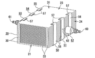
図1〜図4に示されるように、本実施形態のプラズマリアクタ1は、自動車のエンジン(図示略)の排ガスに含まれているPMを除去する装置であり、排気管2に取り付けられている。プラズマリアクタ1は、パルス発生電源3、ケース10及びプラズマパネル積層体20を備えている。   As shown in FIGS. 1 to 4, the plasma reactor 1 of the present embodiment is a device that removes PM contained in exhaust gas of an automobile engine (not shown), and is attached to an exhaust pipe 2. . The plasma reactor 1 includes a pulse generation power source 3, a case 10, and a plasma panel laminate 20.

ケース10は、例えばステンレス鋼を用いて矩形筒状に形成されている。ケース10の熱膨張係数は、10〜18ppm/℃程度となっている。なお、ケース10の熱膨張係数は、常温〜300℃間の測定値の平均値をいう。ケース10の第1端部(図1では左端部)には第1コーン部11が接続され、ケース10の第2端部(図1では右端部)には第2コーン部12が接続されている。さらに、第1コーン部11は、排気管2の上流側部分4(エンジン側の部分)に接続され、第2コーン部12は、排気管2の下流側部分5(エンジン側とは反対側の部分)に接続されている。なお、エンジンからの排ガスは、排気管2の上流側部分4から第1コーン部11を介してケース10内に流入し、ケース10内を通過した後、第2コーン部12を介して排気管2の下流側部分5に流出する。   The case 10 is formed in a rectangular cylinder shape using, for example, stainless steel. The thermal expansion coefficient of the case 10 is about 10 to 18 ppm / ° C. In addition, the thermal expansion coefficient of case 10 says the average value of the measured value between normal temperature and 300 degreeC. A first cone portion 11 is connected to a first end portion (left end portion in FIG. 1) of the case 10, and a second cone portion 12 is connected to a second end portion (right end portion in FIG. 1) of the case 10. Yes. Further, the first cone portion 11 is connected to the upstream portion 4 (engine portion) of the exhaust pipe 2, and the second cone portion 12 is connected to the downstream portion 5 (opposite side of the engine side) of the exhaust pipe 2. Part). The exhaust gas from the engine flows into the case 10 from the upstream portion 4 of the exhaust pipe 2 through the first cone portion 11, passes through the case 10, and then passes through the second cone portion 12 to the exhaust pipe. 2 flows out to the downstream part 5.

図1,図3〜図8に示されるように、プラズマパネル積層体20は、ケース10内に収容されており、一対のガス通過面21,22と、4つのガス非通過面23,24,25,26とを有する略直方体状を成している。両ガス通過面21,22は、プラズマパネル積層体20において互いに反対側に位置している。一方、各ガス非通過面23〜26は、一対のガス通過面21,22の間に位置している。   As shown in FIGS. 1 and 3 to 8, the plasma panel laminate 20 is housed in the case 10, and includes a pair of gas passage surfaces 21 and 22 and four gas non-passage surfaces 23, 24, 25 and 26 and has a substantially rectangular parallelepiped shape. Both gas passage surfaces 21 and 22 are located on opposite sides of the plasma panel laminate 20. On the other hand, the gas non-passing surfaces 23 to 26 are located between the pair of gas passing surfaces 21 and 22.

また、プラズマパネル積層体20は、複数の電極パネル30を積層した構造を有している。各電極パネル30は、ケース10内における排ガスの通過方向(排ガス流入口11から排ガス流出口12に向かう方向)と平行に配置されており、互いに隙間(本実施形態では、0.5mmの隙間)を有するように配置されている。   The plasma panel laminate 20 has a structure in which a plurality of electrode panels 30 are laminated. Each electrode panel 30 is arranged in parallel with the passage direction of the exhaust gas in the case 10 (the direction from the exhaust gas inlet 11 toward the exhaust gas outlet 12), and is spaced from each other (in this embodiment, a gap of 0.5 mm). It is arranged to have.

図1に示されるように、各電極パネル30には、プラズマパネル積層体20の厚さ方向に沿って第1の配線6及び第2の配線7が交互に電気的に接続されている。第1の配線6は、パルス発生電源3の第1の端子に電気的に接続され、第2の配線7は、パルス発生電源3の第2の端子に電気的に接続されている。   As shown in FIG. 1, the first wiring 6 and the second wiring 7 are alternately and electrically connected to each electrode panel 30 along the thickness direction of the plasma panel laminate 20. The first wiring 6 is electrically connected to the first terminal of the pulse generating power supply 3, and the second wiring 7 is electrically connected to the second terminal of the pulse generating power supply 3.

図1,図9に示されるように、本実施形態の電極パネル30は、第1主面31及び第2主面32を有し、縦100mm×横200mmの略矩形板状を成している。第1主面31及び第2主面32は、電極パネル30の厚さ方向において互いに反対側に位置している。さらに、電極パネル30は、矩形板状の誘電体33に放電電極34(厚さ10μm)を内蔵してなる構造を有している。本実施形態において、誘電体33はアルミナ(Al)等のセラミックからなり、放電電極34はタングステン(W)からなる。また、誘電体33の熱膨張係数は、2〜8ppm/℃程度であり、誘電体33がアルミナからなる本実施形態においては、7ppm/℃程度となっている。なお、誘電体33の熱膨張係数は、常温〜400℃間の測定値の平均値をいう。また、誘電体33は、第2主面32にて開口する凹部35を有している。凹部35は、電極パネル30の横方向に延びており、電極パネル30の両端面にて開口している。本実施形態のプラズマパネル積層体20では、凹部35と下層側に隣接する電極パネル30の第1主面31とによって、排ガスの流路が構成される。なお、プラズマパネル積層体20を構成する最下層の電極パネル30には、下層側に電極パネル30が存在しないため、凹部35が形成されていない。 As shown in FIG. 1 and FIG. 9, the electrode panel 30 of the present embodiment has a first main surface 31 and a second main surface 32 and has a substantially rectangular plate shape of 100 mm long × 200 mm wide. . The first main surface 31 and the second main surface 32 are located on opposite sides in the thickness direction of the electrode panel 30. Further, the electrode panel 30 has a structure in which a discharge electrode 34 (thickness 10 μm) is built in a rectangular plate-like dielectric 33. In the present embodiment, the dielectric 33 is made of ceramic such as alumina (Al 2 O 3 ), and the discharge electrode 34 is made of tungsten (W). In addition, the thermal expansion coefficient of the dielectric 33 is about 2 to 8 ppm / ° C., and in the present embodiment in which the dielectric 33 is made of alumina, it is about 7 ppm / ° C. The thermal expansion coefficient of the dielectric 33 is an average value of measured values between room temperature and 400 ° C. In addition, the dielectric 33 has a recess 35 that opens at the second main surface 32. The recess 35 extends in the lateral direction of the electrode panel 30 and opens at both end faces of the electrode panel 30. In the plasma panel laminate 20 of the present embodiment, the exhaust gas flow path is constituted by the recess 35 and the first main surface 31 of the electrode panel 30 adjacent to the lower layer side. The lowermost electrode panel 30 constituting the plasma panel laminate 20 is not formed with the recess 35 because the electrode panel 30 does not exist on the lower layer side.

図9に示されるように、電極パネル30における凹部35の両側部分には、第1主面31側と第2主面32側とを導通させる導通構造40がそれぞれ設けられている。各導通構造40は、スルーホール導体41、第1パッド42及び第2パッド43を備えている。スルーホール導体41は、第1主面31及び第2主面32を貫通している。そして、一方の導通構造40に設けられたスルーホール導体41は、第1主面31及び第2主面32に加えて、放電電極34から外周側に延出する延出部36を貫通している。また、第1パッド42は、第1主面31に形成されており、スルーホール導体41の第1主面31側端部に電気的に接続されている。一方、第2パッド43は、第2主面32に形成されており、スルーホール導体41の第2主面32側端部に電気的に接続されている。なお、第1パッド42及び第2パッド43は、それぞれ長方形状を成しており、表面にNi等のめっきが施されている。   As shown in FIG. 9, conductive structures 40 that connect the first main surface 31 side and the second main surface 32 side are respectively provided on both side portions of the recess 35 in the electrode panel 30. Each conduction structure 40 includes a through-hole conductor 41, a first pad 42, and a second pad 43. The through-hole conductor 41 passes through the first main surface 31 and the second main surface 32. And the through-hole conductor 41 provided in one conduction | electrical_connection structure 40 penetrates the extension part 36 extended in the outer peripheral side from the discharge electrode 34 in addition to the 1st main surface 31 and the 2nd main surface 32. Yes. The first pad 42 is formed on the first main surface 31 and is electrically connected to the end of the through-hole conductor 41 on the first main surface 31 side. On the other hand, the second pad 43 is formed on the second main surface 32 and is electrically connected to the end of the through-hole conductor 41 on the second main surface 32 side. The first pad 42 and the second pad 43 each have a rectangular shape, and the surface thereof is plated with Ni or the like.

図7,図8に示されるように、プラズマリアクタ1は、各電極パネル30(プラズマパネル積層体20)を外側(具体的には、ガス非通過面24側)から挟み込んで固定する3つの第1クランプ50,51,52と、各電極パネル30を外側(具体的には、ガス非通過面26側)から挟み込んで固定する3つの第2クランプ53,54,55とを備えている。各クランプ50〜55は、金属板(例えばステンレス板)を折り曲げることによって形成されている。また、各第1クランプ50〜52は、ガス非通過面24において、プラズマパネル積層体20の横方向(電極パネル30の積層方向に対して垂直な方向)に沿って等間隔に配置され、各第2クランプ53〜55は、ガス非通過面26において、プラズマパネル積層体20の横方向に沿って等間隔に配置されている。なお、第1クランプ50〜52のうちガス非通過面24の中央部分に配置された第1クランプ51、及び、第2クランプ53〜55のうちガス非通過面26の中央部分に配置された第2クランプ54は、各電極パネル30を積層方向に挟み込む機能に加えて、放電電極34に電気的に接続される電気導通部材としての機能を有している。一方、第1クランプ50〜52のうちガス非通過面24の両側部分に配置された第1クランプ50,52、及び、第2クランプ53〜55のうちガス非通過面26の両側部分に配置された第2クランプ53,55は、各電極パネル30を積層方向に挟み込む機能のみを有している。   As shown in FIG. 7 and FIG. 8, the plasma reactor 1 includes three third electrodes that sandwich and fix each electrode panel 30 (plasma panel laminate 20) from the outside (specifically, the gas non-passing surface 24 side). 1 clamp 50, 51, 52 and three 2nd clamps 53, 54, 55 which clamp and fix each electrode panel 30 from the outside (specifically, the gas non-passing surface 26 side). Each clamp 50-55 is formed by bending a metal plate (for example, stainless steel plate). The first clamps 50 to 52 are arranged at equal intervals along the horizontal direction of the plasma panel stack 20 (direction perpendicular to the stacking direction of the electrode panel 30) on the gas non-passing surface 24. The second clamps 53 to 55 are arranged at equal intervals along the horizontal direction of the plasma panel stack 20 on the gas non-passing surface 26. In addition, the 1st clamp 51 arrange | positioned in the center part of the gas non-passing surface 24 among the 1st clamps 50-52 and the 1st clamp arrange | positioned in the center part of the gas non-passing surface 26 among the 2nd clamps 53-55. The two clamps 54 have a function as an electrically conductive member that is electrically connected to the discharge electrode 34 in addition to the function of sandwiching each electrode panel 30 in the stacking direction. On the other hand, among the first clamps 50 to 52, the first clamps 50 and 52 disposed on both sides of the gas non-passing surface 24 and the second clamps 53 to 55 are disposed on both sides of the gas non-passing surface 26. The second clamps 53 and 55 have only a function of sandwiching each electrode panel 30 in the stacking direction.

また、図7,図8に示されるように、各クランプ50〜55は、クランプ本体56及び押さえ板57を備えている。クランプ本体56は、電極パネル30の積層方向に延びている。押さえ板57は、クランプ本体56と一体に形成され、クランプ本体56の両端部に配置されている。各押さえ板57は、弾性を有しており、折り返し構造を有する板ばねである。なお、各クランプ50〜55を構成する両押さえ板57は、プラズマパネル積層体20のガス非通過面23とガス非通過面25とにそれぞれ圧接している。そして、クランプ51,54を構成する両押さえ板57は、ガス非通過面23(最上層の電極パネル30の第1主面31)に形成された第1パッド42と、ガス非通過面25(最下層の電極パネル30の第2主面32)に形成された第2パッド43とに圧接している。   As shown in FIGS. 7 and 8, each of the clamps 50 to 55 includes a clamp body 56 and a pressing plate 57. The clamp body 56 extends in the stacking direction of the electrode panels 30. The holding plate 57 is formed integrally with the clamp body 56 and is disposed at both ends of the clamp body 56. Each pressing plate 57 is a leaf spring having elasticity and a folded structure. Note that the pressing plates 57 constituting the clamps 50 to 55 are in pressure contact with the gas non-passing surface 23 and the gas non-passing surface 25 of the plasma panel laminate 20, respectively. The pressing plates 57 constituting the clamps 51 and 54 are provided with a first pad 42 formed on the gas non-passing surface 23 (the first main surface 31 of the uppermost electrode panel 30) and the gas non-passing surface 25 ( It is in pressure contact with the second pad 43 formed on the second main surface 32) of the lowermost electrode panel 30.

図2〜図8に示されるように、プラズマリアクタ1は、一対の外部端子60,61を備えている。本実施形態の外部端子60,61は、スパークプラグと同様の構造を有している。詳述すると、外部端子60,61は、外部接続部、金属粉末を含む導電性シール、絶縁体、主体金具、滑石、パッキン類等を備えている。外部接続部は、導電性シールを介して中軸62に接続されている。なお、外部端子は、本実施形態のものに限定される訳ではなく、絶縁体によって外部接続部とケース10との間が絶縁されている構造であれば、他の構造であってもよい。   As shown in FIGS. 2 to 8, the plasma reactor 1 includes a pair of external terminals 60 and 61. The external terminals 60 and 61 of this embodiment have the same structure as a spark plug. More specifically, the external terminals 60 and 61 include an external connection portion, a conductive seal containing metal powder, an insulator, a metal shell, talc, packing, and the like. The external connection portion is connected to the middle shaft 62 via a conductive seal. The external terminal is not limited to the one in the present embodiment, and may have another structure as long as the external connection portion and the case 10 are insulated by an insulator.

また、外部端子60は、基端部が第1クランプ51のクランプ本体56に電気的に接続され、先端部がケース10から露出している(図2〜図4参照)。同様に、外部端子61は、基端部が第2クランプ54のクランプ本体56に電気的に接続され、先端部がケース10から露出している。即ち、外部端子60は、プラズマパネル積層体20のガス非通過面24に配置され、外部端子61は、ガス非通過面24とは反対側に位置するガス非通過面26に配置されている。そして、各外部端子60,61は、互いに反対方向に突出している。なお、本実施形態では、外部端子60の先端部が第1の配線6(図1参照)に接続されるとともに、外部端子61の先端部が第2の配線7(図1参照)に接続されるようになっている。   In addition, the external terminal 60 is electrically connected to the clamp main body 56 of the first clamp 51 at the proximal end portion, and the distal end portion is exposed from the case 10 (see FIGS. 2 to 4). Similarly, the external terminal 61 is electrically connected to the clamp main body 56 of the second clamp 54 at the proximal end portion, and the distal end portion is exposed from the case 10. That is, the external terminal 60 is disposed on the gas non-passing surface 24 of the plasma panel laminate 20, and the external terminal 61 is disposed on the gas non-passing surface 26 located on the opposite side of the gas non-passing surface 24. The external terminals 60 and 61 protrude in opposite directions. In the present embodiment, the tip of the external terminal 60 is connected to the first wiring 6 (see FIG. 1), and the tip of the external terminal 61 is connected to the second wiring 7 (see FIG. 1). It has become so.

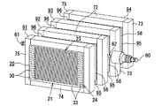
図3〜図6に示されるように、ケース10とプラズマパネル積層体20との間には、側面視で矩形環状をなすマット71が介在されている。マット71は、プラズマパネル積層体20をケース10に固定する機能を有している。また、マット71は、プラズマパネル積層体20の外表面を覆っている。詳述すると、マット71は、ガス非通過面23を覆う略矩形板状の第1マット片72と、ガス非通過面24を覆う略矩形板状の第2マット片73と、ガス非通過面25を覆う略矩形板状の第3マット片74と、ガス非通過面26を覆う略矩形板状の第4マット片75とによって構成されている。マット71は、各マット片72〜75を、必要に応じて、接着テープ等を用いて互いに接合することにより構成される。ここで、マット71を構成する材料としては、例えば、セラミック繊維、金属繊維、発泡金属等の絶縁材料を用いることができる。   As shown in FIGS. 3 to 6, a mat 71 having a rectangular ring shape when viewed from the side is interposed between the case 10 and the plasma panel laminate 20. The mat 71 has a function of fixing the plasma panel laminate 20 to the case 10. Further, the mat 71 covers the outer surface of the plasma panel laminate 20. Specifically, the mat 71 includes a substantially rectangular plate-shaped first mat piece 72 covering the gas non-passing surface 23, a substantially rectangular plate-shaped second mat piece 73 covering the gas non-passing surface 24, and a gas non-passing surface. 25, a third mat piece 74 having a substantially rectangular plate shape covering 25, and a fourth mat piece 75 having a substantially rectangular plate shape covering the gas non-passing surface 26. The mat 71 is configured by bonding the mat pieces 72 to 75 to each other using an adhesive tape or the like as necessary. Here, as a material constituting the mat 71, for example, an insulating material such as ceramic fiber, metal fiber, and foam metal can be used.

また、図5,図6に示されるように、本実施形態のプラズマリアクタ1は、マット71とクランプ50〜55との間に隙間を有している。本実施形態のマット71には、同マット71を厚さ方向に貫通する3つの第1切欠部81が形成されるとともに、マット71を厚さ方向に貫通する3つの第2切欠部82が形成されている。そして、各第1切欠部81の内側領域にそれぞれ第1クランプ50,51,52が位置するとともに、各第2切欠部82の内側領域にそれぞれ第2クランプ53,54,55が位置するようになっている。   As shown in FIGS. 5 and 6, the plasma reactor 1 of the present embodiment has a gap between the mat 71 and the clamps 50 to 55. In the mat 71 of the present embodiment, three first notches 81 penetrating the mat 71 in the thickness direction are formed, and three second notches 82 penetrating the mat 71 in the thickness direction are formed. Has been. The first clamps 50, 51, 52 are located in the inner regions of the first notches 81, and the second clamps 53, 54, 55 are located in the inner regions of the second notches 82, respectively. It has become.

詳述すると、第1切欠部81は、第2マット片73を厚方向に貫通する第1溝部83と、マット片72,74をそれぞれ厚さ方向に貫通する一対の第1凹部84とからなっている。第1溝部83は、電極パネル30の積層方向に沿って延びており、第2マット片73を分断している。一方、第1凹部84は、マット片72,74の外周部の一部のみに形成されており、マット片72,74を分断しないようになっている。なお、第1溝部83内には、第1クランプ50〜52のクランプ本体56と外部端子60の基端部に接続される中軸62とが配置され、第1凹部84内には、第1クランプ50〜52の押さえ板57が配置されている。   More specifically, the first notch 81 includes a first groove 83 that penetrates the second mat piece 73 in the thickness direction and a pair of first recesses 84 that respectively penetrate the mat pieces 72 and 74 in the thickness direction. ing. The first groove 83 extends along the stacking direction of the electrode panel 30 and divides the second mat piece 73. On the other hand, the 1st recessed part 84 is formed only in a part of outer peripheral part of the mat pieces 72 and 74, and the mat pieces 72 and 74 are not divided. In the first groove 83, the clamp body 56 of the first clamps 50 to 52 and the center shaft 62 connected to the proximal end portion of the external terminal 60 are disposed, and in the first recess 84, the first clamp 50 to 52 pressing plates 57 are arranged.

そして、図5に示されるように、本実施形態のプラズマリアクタ1では、マット71と第1クランプ50〜52との間(具体的に言うと、第1溝部83の内壁面とクランプ本体56の側縁との間、及び、第1凹部84の内側面と押さえ板57の外周縁との間)に、第1の隙間S1を有している。第1の隙間S1の大きさは、0.5mm以上30mm以下(本実施形態では、最小で5mm)に設定されている。   As shown in FIG. 5, in the plasma reactor 1 of the present embodiment, between the mat 71 and the first clamps 50 to 52 (specifically, the inner wall surface of the first groove 83 and the clamp body 56). A first gap S <b> 1 is provided between the side edges and between the inner side surface of the first recess 84 and the outer peripheral edge of the pressing plate 57. The magnitude | size of 1st clearance gap S1 is set to 0.5 mm or more and 30 mm or less (5 mm in this embodiment at the minimum).

図5,図6に示されるように、第2切欠部82は、第4マット片75を厚さ方向に貫通する第2溝部85と、マット片72,74をそれぞれ厚さ方向に貫通する一対の第2凹部86とからなっている。第2溝部85は、電極パネル30の積層方向に沿って延びており、第4マット片75を分断している。一方、第2凹部86は、マット片72,74の外周部の一部のみに形成されており、マット片72,74を分断しないようになっている。なお、第2溝部85内には、第2クランプ53〜55のクランプ本体56と外部端子61の基端部に接続される中軸62とが配置され、第2凹部86内には、第2クランプ53〜55の押さえ板57が配置されている。   As shown in FIGS. 5 and 6, the second notch portion 82 includes a second groove portion 85 that penetrates the fourth mat piece 75 in the thickness direction, and a pair that penetrates the mat pieces 72 and 74 in the thickness direction. The second recess 86. The second groove 85 extends along the stacking direction of the electrode panel 30 and divides the fourth mat piece 75. On the other hand, the second recess 86 is formed only in a part of the outer peripheral portion of the mat pieces 72 and 74 so that the mat pieces 72 and 74 are not divided. A clamp body 56 of the second clamps 53 to 55 and a middle shaft 62 connected to the proximal end portion of the external terminal 61 are disposed in the second groove 85, and the second clamp 86 has a second clamp 86. 53 to 55 pressing plates 57 are arranged.

そして、本実施形態のプラズマリアクタ1では、マット71と第2クランプ53〜55との間(具体的に言うと、第2溝部85の内壁面とクランプ本体56の側縁との間、及び、第2凹部86の内側面と押さえ板57の外周縁との間)に、第2の隙間S2を有している。第2の隙間S2の大きさは、第1の隙間S1の大きさと等しくなっており、0.5mm以上30mm以下(本実施形態では、最小で5mm)に設定されている。   In the plasma reactor 1 of the present embodiment, between the mat 71 and the second clamps 53 to 55 (specifically, between the inner wall surface of the second groove 85 and the side edge of the clamp body 56, and A second gap S <b> 2 is provided between the inner side surface of the second recess 86 and the outer peripheral edge of the pressing plate 57. The size of the second gap S2 is equal to the size of the first gap S1, and is set to 0.5 mm or more and 30 mm or less (in this embodiment, 5 mm at the minimum).

さらに、図4,図5に示されるように、本実施形態のプラズマリアクタ1は、マット71とクランプ50〜55との間に加えて、ケース10とクランプ50〜55との間にも隙間を有している。詳述すると、マット71の厚さは8mmであり、クランプ50〜55の厚さは0.5mmである。このため、ケース10と第1クランプ50〜52との間(具体的に言うと、ケース10の内面と第1クランプ50〜52のクランプ本体56表面との間、及び、ケース10の内面と第1クランプ50〜52の押さえ板57表面との間)には、第1の隙間S3が設けられるようになる。さらに、ケース10と第2クランプ53〜55との間(具体的に言うと、ケース10の内面と第2クランプ53〜55のクランプ本体56表面との間、及び、ケース10の内面と第2クランプ53〜55の押さえ板57表面との間)には、第2の隙間S4が設けられるようになる。なお、本実施形態の隙間S3,S4の大きさは、7.5mm程度となっている。   Furthermore, as shown in FIGS. 4 and 5, the plasma reactor 1 of the present embodiment has a gap between the case 10 and the clamps 50 to 55 in addition to the gap between the mat 71 and the clamps 50 to 55. Have. More specifically, the mat 71 has a thickness of 8 mm, and the clamps 50 to 55 have a thickness of 0.5 mm. Therefore, between the case 10 and the first clamps 50 to 52 (specifically, between the inner surface of the case 10 and the surface of the clamp body 56 of the first clamps 50 to 52, and between the inner surface of the case 10 and the first clamp 50-52). A first gap S3 is provided between the surface of the pressing plate 57 of each clamp 50-52. Furthermore, between the case 10 and the second clamps 53 to 55 (specifically, between the inner surface of the case 10 and the surface of the clamp body 56 of the second clamps 53 to 55, and between the inner surface of the case 10 and the second clamp A second gap S4 is provided between the surfaces of the clamp plates 53 to 55 and the pressing plate 57. In addition, the size of the gaps S3 and S4 in this embodiment is about 7.5 mm.

図1に示されるように、本実施形態のプラズマリアクタ1は、例えば、排ガスに含まれているPMを除去するために用いられる。この場合、パルス発生電源3から互いに隣接する電極パネル30間にパルス電圧(例えば、ピーク電圧:5kV(5000V)、パルス繰返し周波数:100Hz)が印加されると、誘電体バリア放電が生じ、放電電極34間に誘電体バリア放電によるプラズマが発生する。そして、プラズマの発生により、放電電極34間を流通する排ガスに含まれるPMが酸化(燃焼)されて除去される。   As shown in FIG. 1, the plasma reactor 1 of the present embodiment is used, for example, to remove PM contained in exhaust gas. In this case, when a pulse voltage (for example, peak voltage: 5 kV (5000 V), pulse repetition frequency: 100 Hz) is applied between the electrode panels 30 adjacent to each other from the pulse generating power supply 3, dielectric barrier discharge occurs, and the discharge electrode 34 generates plasma due to dielectric barrier discharge. Due to the generation of plasma, PM contained in the exhaust gas flowing between the discharge electrodes 34 is oxidized (burned) and removed.

次に、プラズマリアクタ1の製造方法を説明する。   Next, a method for manufacturing the plasma reactor 1 will be described.

まず、アルミナ粉末を主成分とするセラミック材料を用いて、誘電体33となる第1〜第3のセラミックグリーンシートを形成する。なお、セラミックグリーンシートの形成方法としては、テープ成形や押出成形などの周知の成形法を用いることができる。そして、各セラミックグリーンシートに対してレーザ加工を行い、所定の位置に貫通孔を形成する。なお、貫通孔の形成は、パンチング加工、ドリル加工等によって行ってもよい。   First, the 1st-3rd ceramic green sheet used as the dielectric material 33 is formed using the ceramic material which has an alumina powder as a main component. In addition, as a formation method of a ceramic green sheet, well-known shaping | molding methods, such as tape shaping | molding and extrusion molding, can be used. And each ceramic green sheet is laser-processed and a through-hole is formed in a predetermined position. The through hole may be formed by punching, drilling, or the like.

次に、従来周知のペースト印刷装置(図示略)を用いて、各セラミックグリーンシートの貫通孔に導電性ペースト(本実施形態では、タングステンペースト)を充填し、スルーホール導体41となる未焼成のスルーホール導体部を形成する。   Next, using a conventionally known paste printing apparatus (not shown), the through holes of each ceramic green sheet are filled with a conductive paste (in this embodiment, a tungsten paste), and an unfired portion that becomes the through-hole conductor 41 is obtained. A through-hole conductor is formed.

次に、第1のセラミックグリーンシートを支持台(図示略)に載置する。さらに、ペースト印刷装置を用いて、第1のセラミックグリーンシートの裏面上に導電性ペーストを印刷する。その結果、第1のセラミックグリーンシートの裏面上に、放電電極34となる厚さ10μmの未焼成電極が形成される。なお、第1のセラミックグリーンシートに対する未焼成電極の印刷方法としては、スクリーン印刷などの周知の印刷法を使用することができる。   Next, the first ceramic green sheet is placed on a support base (not shown). Furthermore, a conductive paste is printed on the back surface of the first ceramic green sheet using a paste printing apparatus. As a result, an unsintered electrode having a thickness of 10 μm to be the discharge electrode 34 is formed on the back surface of the first ceramic green sheet. In addition, as a printing method of the unsintered electrode with respect to the 1st ceramic green sheet, well-known printing methods, such as screen printing, can be used.

そして、導電性ペーストを乾燥後、未焼成電極が印刷された第1のセラミックグリーンシートの裏面上に、第2のセラミックグリーンシート及び第3のセラミックグリーンシートを順番に積層し、シート積層方向に押圧力を付与する。その結果、各セラミックグリーンシートが一体化され、セラミック積層体が形成される。さらに、ペースト印刷装置を用いて、第1のセラミックグリーンシートの主面上に導電性ペーストを印刷し、未焼成の第1パッド42を形成するとともに、第3のセラミックグリーンシートの裏面上に導電性ペーストを印刷し、未焼成の第2パッド43を形成する。なお、第3のセラミックグリーンシートは、凹部35の形状に合わせた打抜加工を施した後に積層される。   Then, after drying the conductive paste, the second ceramic green sheet and the third ceramic green sheet are sequentially laminated on the back surface of the first ceramic green sheet on which the unfired electrodes are printed, and in the sheet lamination direction. Apply pressing force. As a result, the ceramic green sheets are integrated to form a ceramic laminate. Further, using a paste printing device, a conductive paste is printed on the main surface of the first ceramic green sheet to form the unfired first pad 42 and conductive on the back surface of the third ceramic green sheet. The non-sintered second pad 43 is formed by printing the conductive paste. The third ceramic green sheet is laminated after being subjected to a punching process that matches the shape of the recess 35.

次に、周知の手法に従って乾燥工程や脱脂工程などを行った後、セラミック積層体(セラミックグリーンシート及び未焼成電極)をアルミナ及びタングステンが焼結しうる所定の温度(例えば1400℃〜1600℃程度)に加熱する同時焼成を行う。その結果、セラミックグリーンシート中のアルミナ、及び、導電性ペースト中のタングステンが同時焼結し、誘電体33、放電電極34、スルーホール導体41、第1パッド42及び第2パッド43が同時焼成によって形成され、セラミック積層体が電極パネル30となる。   Next, after performing a drying process, a degreasing process, and the like according to a well-known method, a predetermined temperature (for example, about 1400 ° C. to 1600 ° C.) at which the ceramic laminate (ceramic green sheet and green electrode) can be sintered by alumina and tungsten. ) Is simultaneously fired. As a result, alumina in the ceramic green sheet and tungsten in the conductive paste are simultaneously sintered, and the dielectric 33, the discharge electrode 34, the through-hole conductor 41, the first pad 42, and the second pad 43 are simultaneously fired. The formed ceramic laminate becomes the electrode panel 30.

その後、得られた電極パネル30を複数枚積層し、プラズマパネル積層体20を形成する。次に、クランプ50〜55を用いて、複数の電極パネル30を積層方向に挟み込んで固定する。このとき、クランプ51,54を構成する一対の押さえ板57が、第1パッド42と第2パッド43とに圧接する。さらに、溶接等を行うことにより、第1クランプ51を構成するクランプ本体56に中軸62を介して外部端子60の基端部を接続するとともに、第2クランプ54を構成するクランプ本体56に中軸62を介して外部端子61の基端部を接続する。次に、プラズマパネル積層体20の外表面を覆うようにマット71を取り付けた後、マット71の外表面を覆うようにケース10を取り付ける。その後、外部端子60の先端部に第1の配線6を接続するとともに、外部端子61の先端部に第2の配線7を接続する。以上のプロセスを経て、プラズマリアクタ1が完成する。   Thereafter, a plurality of obtained electrode panels 30 are laminated to form a plasma panel laminate 20. Next, the clamps 50 to 55 are used to sandwich and fix the plurality of electrode panels 30 in the stacking direction. At this time, the pair of pressing plates 57 constituting the clamps 51 and 54 are in pressure contact with the first pad 42 and the second pad 43. Further, by performing welding or the like, the proximal end portion of the external terminal 60 is connected to the clamp body 56 constituting the first clamp 51 via the middle shaft 62, and the middle shaft 62 is connected to the clamp body 56 constituting the second clamp 54. The base end of the external terminal 61 is connected via Next, after attaching the mat 71 so as to cover the outer surface of the plasma panel laminate 20, the case 10 is attached so as to cover the outer surface of the mat 71. Thereafter, the first wiring 6 is connected to the distal end portion of the external terminal 60, and the second wiring 7 is connected to the distal end portion of the external terminal 61. The plasma reactor 1 is completed through the above processes.

従って、本実施形態によれば以下の効果を得ることができる。   Therefore, according to the present embodiment, the following effects can be obtained.

(1)本実施形態のプラズマリアクタ1では、マット71とクランプ50〜55との間に隙間S1,S2を有するとともに、ケース10とクランプ50〜55との間に隙間S3,S4を有している。このため、高温の排気ガスの流入時において、ケース10とプラズマパネル積層体20との熱膨張差に起因する応力が生じたとしても、マット71及びケース10からクランプ50〜55に対して応力が作用しにくくなるため、クランプ50〜55の変形や破壊が抑制される。ゆえに、プラズマリアクタ1の信頼性を向上させることができる。   (1) In the plasma reactor 1 of the present embodiment, the gaps S1 and S2 are provided between the mat 71 and the clamps 50 to 55, and the gaps S3 and S4 are provided between the case 10 and the clamps 50 to 55. Yes. For this reason, even when a stress caused by a difference in thermal expansion between the case 10 and the plasma panel laminate 20 occurs when high-temperature exhaust gas flows in, stress is applied from the mat 71 and the case 10 to the clamps 50 to 55. Since it becomes difficult to act, the deformation | transformation and destruction of the clamps 50-55 are suppressed. Therefore, the reliability of the plasma reactor 1 can be improved.

(2)本実施形態では、マット71に対してクランプ50〜55を避けるように切欠部81,82を形成することにより、マット71とクランプ50〜55との間に隙間S1,S2を設けている。このため、例えば、複数のマット間にクランプを配置するなどして、マットとクランプとの間に隙間を設ける場合よりも、プラズマリアクタ1の部品点数を減らすることができる。   (2) In the present embodiment, the notches 81 and 82 are formed on the mat 71 so as to avoid the clamps 50 to 55, thereby providing the gaps S1 and S2 between the mat 71 and the clamps 50 to 55. Yes. For this reason, for example, the number of parts of the plasma reactor 1 can be reduced as compared with the case where a gap is provided between the mat and the clamp by arranging clamps between the plurality of mats.

(3)本実施形態のプラズマリアクタ1は、第1コーン部11及び第2コーン部12を介して排気管2に取り付けられている。その結果、排気管2の上流側部分4→第1コーン部11→プラズマリアクタ1→第2コーン部12→排気管2の下流側部分5の順番に排ガスが流れる排ガス流路内の抵抗が低減されるため、排ガス流路内における圧力損失を抑えることができる。ひいては、圧力損失に伴うエンジンの出力低下も防止することができる。   (3) The plasma reactor 1 of this embodiment is attached to the exhaust pipe 2 via the first cone portion 11 and the second cone portion 12. As a result, the resistance in the exhaust gas flow path in which the exhaust gas flows in the order of the upstream portion 4 of the exhaust pipe 2 → the first cone portion 11 → the plasma reactor 1 → the second cone portion 12 → the downstream portion 5 of the exhaust pipe 2 is reduced. Therefore, the pressure loss in the exhaust gas passage can be suppressed. As a result, it is possible to prevent the engine output from decreasing due to pressure loss.

なお、上記実施形態を以下のように変更してもよい。   In addition, you may change the said embodiment as follows.

・上記実施形態では、マット71に切欠部81,82を形成し、切欠部81,82の内側領域にクランプ50〜55を位置させることにより、マット71とクランプ50〜55との間に隙間S1,S2を設けていたが、他の構造によって隙間を設けてもよい。例えば、図10,図11に示されるように、4つのマット91,92,93,94を互いに離間して配置することにより、各マット91〜94を完全に分断し、隣接するマット91〜94間にクランプ95,96を配置することにより、マット91〜94とクランプ95,96との間に隙間S5を設けるようにしてもよい。また、マットの内面に、クランプと接触する領域との間にクランプ逃げ部(図示略)を設け、マットとクランプとの間に隙間を生じさせるようにしてもよい。   In the above embodiment, the notches 81 and 82 are formed in the mat 71, and the clamps 50 to 55 are positioned in the inner region of the notches 81 and 82, whereby the gap S1 is provided between the mat 71 and the clamps 50 to 55. , S2 is provided, but a gap may be provided by another structure. For example, as shown in FIGS. 10 and 11, the four mats 91, 92, 93, 94 are arranged apart from each other, thereby completely dividing each mat 91-94, and adjacent mats 91-94. You may make it provide the clearance gap S5 between the mats 91-94 and the clamps 95 and 96 by arrange | positioning the clamps 95 and 96 between them. Further, a clamp relief portion (not shown) may be provided on the inner surface of the mat between the area in contact with the clamp and a gap may be generated between the mat and the clamp.

・上記実施形態のプラズマリアクタ1では、切欠部81,82の内側面とクランプ50〜55の外周縁との間に隙間S1,S2を有していたが、隙間S1,S2を省略し、切欠部81,82の内側面とクランプ50〜55の外周縁とを互いに接触させてもよい。   In the plasma reactor 1 of the above embodiment, the gaps S1 and S2 are provided between the inner side surfaces of the notches 81 and 82 and the outer peripheral edges of the clamps 50 to 55. However, the gaps S1 and S2 are omitted, and the notches The inner side surfaces of the portions 81 and 82 and the outer peripheral edges of the clamps 50 to 55 may be brought into contact with each other.

・上記実施形態のマット71は、複数のマット片72〜75を、必要に応じて、接着テープ等を用いて互いに接合することにより構成されていたが、他の手法を用いてマットを構成してもよい。例えば、図12に示されるように、マット片101の外周部に設けた凸部102を、隣接するマット片103の外周部に形成した凹部104に嵌合させることにより、マット100を構成してもよい。   The mat 71 of the above embodiment is configured by joining a plurality of mat pieces 72 to 75 to each other using an adhesive tape or the like, if necessary. However, the mat 71 is configured by using other methods. May be. For example, as shown in FIG. 12, the mat 100 is configured by fitting the convex portion 102 provided on the outer peripheral portion of the mat piece 101 into the concave portion 104 formed on the outer peripheral portion of the adjacent mat piece 103. Also good.

・上記実施形態のプラズマリアクタ1は、マット71とクランプ50〜55との間に隙間S1,S2を有するとともに、ケース10とクランプ50〜55との間に隙間S3,S4を有していた。しかし、プラズマリアクタは、ケース10とクランプ50〜55との間のみに隙間を有するものであってもよい。具体的に言うと、例えば、図13に示されるように、ケース111の内面に逃げ凹部112を設け、ケース111とマット113においてクランプ114と接触する領域との間、即ち、ケース111とクランプ114との間に隙間S6を生じさせるようにしてもよい。また、図14に示されるように、マット121においてクランプ122に対応する領域A1を、他の領域よりも薄く形成することにより、ケースとマット121との間、即ち、ケースとクランプ122との間に隙間を設けるようにしてもよい。   The plasma reactor 1 of the above embodiment has the gaps S1 and S2 between the mat 71 and the clamps 50 to 55, and the gaps S3 and S4 between the case 10 and the clamps 50 to 55. However, the plasma reactor may have a gap only between the case 10 and the clamps 50 to 55. More specifically, for example, as shown in FIG. 13, a relief recess 112 is provided on the inner surface of the case 111, and between the case 111 and the area where the mat 113 contacts the clamp 114, that is, the case 111 and the clamp 114. You may make it produce gap S6 between. Further, as shown in FIG. 14, the area A1 corresponding to the clamp 122 in the mat 121 is formed thinner than the other areas, so that the area between the case and the mat 121, that is, between the case and the clamp 122. You may make it provide a clearance gap in.

・上記実施形態の電極パネル30は、誘電体33に放電電極34を内蔵することによって構成されていた。しかし、誘電体33の表面に放電電極34を形成することによって電極パネルを構成してもよい。   -The electrode panel 30 of the said embodiment was comprised by incorporating the discharge electrode 34 in the dielectric material 33. FIG. However, the electrode panel may be configured by forming the discharge electrode 34 on the surface of the dielectric 33.

・上記実施形態のプラズマリアクタ1は、自動車のエンジンの排ガス浄化に用いられていたが、例えば、船舶等の排ガス浄化に用いてもよい。また、プラズマリアクタ1は、プラズマ処理を行うものであればよく、排ガスの処理を行うものでなくてもよいし、浄化に用いるものでなくてもよい。   -Although the plasma reactor 1 of the said embodiment was used for the exhaust gas purification of the engine of a motor vehicle, you may use it for exhaust gas purification, such as a ship, for example. Moreover, the plasma reactor 1 should just perform a plasma process, and does not need to perform the process of waste gas, and does not need to be used for purification | cleaning.

次に、特許請求の範囲に記載された技術的思想のほかに、前述した実施形態によって把握される技術的思想を以下に列挙する。   Next, in addition to the technical ideas described in the claims, the technical ideas grasped by the embodiment described above are listed below.

(1)上記手段1において、前記マットに、同マットを厚さ方向に貫通する切欠部が配置され、前記切欠部の内側領域に前記クランプが位置しており、前記切欠部が、前記複数の電極パネルの積層方向に沿って延びていることを特徴とするプラズマリアクタ。   (1) In the above means 1, the mat has a notch that penetrates the mat in the thickness direction, the clamp is located in an inner region of the notch, and the notch has the plurality of notches A plasma reactor, wherein the plasma reactor extends along a direction in which the electrode panels are stacked.

(2)上記手段1において、複数の前記マットが互いに離間して配置されており、隣接する前記マット間に前記クランプが位置していることを特徴とするプラズマリアクタ。   (2) In the above means 1, a plurality of the mats are arranged apart from each other, and the clamp is located between the adjacent mats.

(3)上記手段1において、前記マットは、前記プラズマパネル積層体の外表面を覆っていることを特徴とするプラズマリアクタ。   (3) In the above means 1, the plasma reactor is characterized in that the mat covers the outer surface of the plasma panel laminate.

(4)上記手段1において、前記電極パネルは、第1主面及び第2主面を有しており、前記電極パネルに、前記第1主面側と前記第2主面側とを導通させる導通構造が設けられ、前記導通構造は、前記第1主面及び前記第2主面を貫通するスルーホール導体と、前記第1主面に形成され、前記スルーホール導体の前記第1主面側端部に電気的に接続される第1パッドと、前記第2主面に形成され、前記スルーホール導体の前記第2主面側端部に電気的に接続される第2パッドとを備えることを特徴とするプラズマリアクタ。   (4) In the above means 1, the electrode panel has a first main surface and a second main surface, and the first main surface side and the second main surface side are electrically connected to the electrode panel. A conduction structure is provided, and the conduction structure is formed in the first main surface and the through hole conductor penetrating the first main surface and the second main surface, and the first main surface side of the through hole conductor. A first pad that is electrically connected to the end, and a second pad that is formed on the second main surface and is electrically connected to the end of the through-hole conductor on the second main surface. A plasma reactor characterized by.

1…プラズマリアクタ
10,111…ケース
20…プラズマパネル積層体
30…電極パネル
34…放電電極
50,51,52…クランプとしての第1クランプ
53,54,55…クランプとしての第2クランプ
71,91,92,93,94,100,113,121…マット
81…切欠部としての第1切欠部
82…切欠部としての第2切欠部
95,96,114,122…クランプ
112…逃げ凹部
A1…マットにおいてクランプに対応する領域
S1,S3…隙間としての第1の隙間
S2,S4…隙間としての第2の隙間
S5,S6…隙間
DESCRIPTION OF SYMBOLS 1 ... Plasma reactor 10, 111 ... Case 20 ... Plasma panel laminated body 30 ... Electrode panel 34 ... Discharge electrode 50, 51, 52 ... 1st clamp 53, 54, 55 as a clamp ... 2nd clamp 71, 91 as a clamp , 92, 93, 94, 100, 113, 121... Mat 81... First notch 82 as a notch. Second notch 95, 96, 114, 122... Clamp 112. Region S1, S3 corresponding to the clamp in the first gap S2, S4 as the gap second gaps S5, S6 as the gap

Claims (5)

放電電極を有する複数の電極パネルを積層した構造を有し、隣接する前記電極パネル間に電圧を印加することによってプラズマを発生させるプラズマパネル積層体と、
前記複数の電極パネルを外側から挟み込んで固定するクランプと、
前記プラズマパネル積層体が収容されるケースと、
前記ケース及び前記プラズマパネル積層体の間に介在され、前記プラズマパネル積層体を保持するマットと
を備えるプラズマリアクタであって、
前記マットと前記クランプとの間、及び、前記ケースと前記クランプとの間の少なくとも一方に隙間を有している
ことを特徴とするプラズマリアクタ。
A plasma panel laminate having a structure in which a plurality of electrode panels having discharge electrodes are laminated, and generating plasma by applying a voltage between the adjacent electrode panels;
A clamp that sandwiches and fixes the plurality of electrode panels from the outside;
A case for accommodating the plasma panel laminate;
A plasma reactor comprising a mat interposed between the case and the plasma panel laminate and holding the plasma panel laminate,
A plasma reactor comprising a gap in at least one of the mat and the clamp and between the case and the clamp.
前記クランプは、前記マットとの間に前記隙間を有していることを特徴とする請求項1に記載のプラズマリアクタ。   The plasma reactor according to claim 1, wherein the clamp has the gap between the clamp and the mat. 前記マットに、同マットを厚さ方向に貫通する切欠部が配置され、前記切欠部の内側領域に前記クランプが位置していることを特徴とする請求項1または2に記載のプラズマリアクタ。   3. The plasma reactor according to claim 1, wherein the mat has a notch that passes through the mat in the thickness direction, and the clamp is located in an inner region of the notch. 前記ケースの内面には、前記マットにおいて前記クランプと接触する領域との間に前記隙間を生じさせるための逃げ凹部が設けられていることを特徴とする請求項1または2に記載のプラズマリアクタ。   3. The plasma reactor according to claim 1, wherein an escape recess for generating the gap is provided on an inner surface of the case between the mat and a region in contact with the clamp. 4. 前記マットにおいて前記クランプに対応する領域は、他の領域よりも薄く形成されることにより、前記ケースとの間に前記隙間を有していることを特徴とする請求項1または2に記載のプラズマリアクタ。   3. The plasma according to claim 1, wherein a region corresponding to the clamp in the mat is formed to be thinner than other regions, thereby having the gap between the case and the case. Reactor.
JP2016038750A 2016-03-01 2016-03-01 Plasma reactor Pending JP2017157363A (en)

Priority Applications (1)

Application Number Priority Date Filing Date Title
JP2016038750A JP2017157363A (en) 2016-03-01 2016-03-01 Plasma reactor

Applications Claiming Priority (1)

Application Number Priority Date Filing Date Title
JP2016038750A JP2017157363A (en) 2016-03-01 2016-03-01 Plasma reactor

Publications (1)

Publication Number Publication Date
JP2017157363A true JP2017157363A (en) 2017-09-07

Family

ID=59809895

Family Applications (1)

Application Number Title Priority Date Filing Date
JP2016038750A Pending JP2017157363A (en) 2016-03-01 2016-03-01 Plasma reactor

Country Status (1)

Country Link
JP (1) JP2017157363A (en)

Cited By (1)

* Cited by examiner, † Cited by third party
Publication number Priority date Publication date Assignee Title
JP7044485B2 (en) 2017-06-07 2022-03-30 日本特殊陶業株式会社 Plasma reactor

Citations (5)

* Cited by examiner, † Cited by third party
Publication number Priority date Publication date Assignee Title
US5746051A (en) * 1994-05-11 1998-05-05 Siemens Aktiengesellschaft Device for detoxifying exhaust fumes from mobile equipment
WO2005005798A1 (en) * 2003-07-10 2005-01-20 Ngk Insulators, Ltd. Plasma generating electrode and plasma reactor
JP2006029212A (en) * 2004-07-15 2006-02-02 Toyota Motor Corp Exhaust emission control device
JP2006510187A (en) * 2002-12-13 2006-03-23 ブルー プラネット カンパニー リミテッド Plasma reactor and electrode plate used therefor
JP2009043805A (en) * 2007-08-07 2009-02-26 Sekisui Chem Co Ltd Plasma treatment device

Patent Citations (5)

* Cited by examiner, † Cited by third party
Publication number Priority date Publication date Assignee Title
US5746051A (en) * 1994-05-11 1998-05-05 Siemens Aktiengesellschaft Device for detoxifying exhaust fumes from mobile equipment
JP2006510187A (en) * 2002-12-13 2006-03-23 ブルー プラネット カンパニー リミテッド Plasma reactor and electrode plate used therefor
WO2005005798A1 (en) * 2003-07-10 2005-01-20 Ngk Insulators, Ltd. Plasma generating electrode and plasma reactor
JP2006029212A (en) * 2004-07-15 2006-02-02 Toyota Motor Corp Exhaust emission control device
JP2009043805A (en) * 2007-08-07 2009-02-26 Sekisui Chem Co Ltd Plasma treatment device

Cited By (1)

* Cited by examiner, † Cited by third party
Publication number Priority date Publication date Assignee Title
JP7044485B2 (en) 2017-06-07 2022-03-30 日本特殊陶業株式会社 Plasma reactor

Similar Documents

Publication Publication Date Title
JP2009110752A (en) Plasma generating body, plasma generating apparatus, ozone generating apparatus, and exhaust gas treatment apparatus
WO2017099011A1 (en) Plasma reactor and plasma electrode plate
JP6491749B2 (en) Plasma reactor
WO2017099175A1 (en) Plasma reactor
EP1835789B1 (en) Plasma generating electrode and plasma reactor
WO2017098987A1 (en) Plasma reactor and clamp for laminated body
JP2017157363A (en) Plasma reactor
JP6656008B2 (en) Plasma reactor
JP6738175B2 (en) Plasma reactor
JP2017140575A (en) Plasma reactor
JP7044485B2 (en) Plasma reactor
JP7146439B2 (en) plasma reactor
JP7101521B2 (en) Plasma reactor and its control method
JP6886349B2 (en) Plasma reactor
JP7049777B2 (en) Plasma reactor
JP2017174620A (en) Plasma reactor
JP2019046555A (en) Plasma reactor
JP6867178B2 (en) Plasma reactor
JP6890045B2 (en) Plasma reactor
JPWO2009001961A1 (en) Plasma generator and plasma generator using the same
JP2006181458A (en) Plasma generation electrode and plasma reactor
KR20220019054A (en) Electric Heated Catalytic Converter
JP2008272615A (en) Wiring structure, apparatus and fluid treating apparatus, and vehicle
JP2018123748A (en) Plasma reactor

Legal Events

Date Code Title Description
A621 Written request for application examination

Free format text: JAPANESE INTERMEDIATE CODE: A621

Effective date: 20190226

A977 Report on retrieval

Free format text: JAPANESE INTERMEDIATE CODE: A971007

Effective date: 20191223

A131 Notification of reasons for refusal

Free format text: JAPANESE INTERMEDIATE CODE: A131

Effective date: 20200114

A02 Decision of refusal

Free format text: JAPANESE INTERMEDIATE CODE: A02

Effective date: 20200707