JP2017139403A - Multilayer penetration capacitor and electronic component device - Google Patents
Multilayer penetration capacitor and electronic component device Download PDFInfo
- Publication number
- JP2017139403A JP2017139403A JP2016020649A JP2016020649A JP2017139403A JP 2017139403 A JP2017139403 A JP 2017139403A JP 2016020649 A JP2016020649 A JP 2016020649A JP 2016020649 A JP2016020649 A JP 2016020649A JP 2017139403 A JP2017139403 A JP 2017139403A
- Authority
- JP
- Japan
- Prior art keywords
- grounding
- pair
- electrodes
- mounting
- length
- Prior art date
- Legal status (The legal status is an assumption and is not a legal conclusion. Google has not performed a legal analysis and makes no representation as to the accuracy of the status listed.)
- Pending
Links
Images


Abstract
Description
本発明は、積層貫通コンデンサ及び電子部品装置に関する。 The present invention relates to a multilayer feedthrough capacitor and an electronic component device.
積層貫通コンデンサとして、素体と、素体の外表面に配置された一対の信号用端子電極及び一対の接地用端子電極と、素体内に交互に配置された、それぞれ複数の信号用内部電極及び接地用内部電極と、を備えたものが知られている(たとえば特許文献1参照)。 As a multilayer feedthrough capacitor, an element body, a pair of signal terminal electrodes and a pair of ground terminal electrodes arranged on the outer surface of the element body, and a plurality of signal internal electrodes arranged alternately in the element body and A device including a grounding internal electrode is known (see, for example, Patent Document 1).
本発明は、低ESL(等価直列インダクタンス)化が図られている積層貫通コンデンサ及び電子部品装置を提供することを目的とする。 SUMMARY OF THE INVENTION An object of the present invention is to provide a multilayer feedthrough capacitor and an electronic component device that have a low ESL (equivalent series inductance).
本発明に係る積層貫通コンデンサは、互いに対向する長方形状の第一及び第二主面と、第一及び第二主面間を連結するように第一及び第二主面の短辺方向に延び、かつ、互いに対向する第一及び第二側面と、第一及び第二主面間を連結するように第一及び第二主面の長辺方向に延び、かつ、互いに対向する第三及び第四側面と、を有する素体と、素体の第一及び第二側面側に配置された一対の信号用端子電極と、素体の第三及び第四側面側に配置された一対の接地用端子電極と、素体内に第一及び第二主面の対向方向に交互に配置された、それぞれ複数の信号用内部電極及び接地用内部電極と、を備え、各信号用内部電極は、一対の信号用端子電極に接続され、各接地用内部電極は、一対の接地用端子電極に接続され、素体の長辺方向での長さをL、接地用内部電極の接地用端子電極に接続される接続部の長辺方向での長さをA、接地用端子電極の長辺方向での長さをCとしたとき、
L≦1.6mm
C/L≧0.40
A/L≧0.20
を満たしている。
The multilayer feedthrough capacitor according to the present invention extends in the short side direction of the first and second main surfaces so as to connect the rectangular first and second main surfaces facing each other and the first and second main surfaces. And the first and second side surfaces facing each other and the third and second surfaces extending in the long side direction of the first and second main surfaces so as to connect the first and second main surfaces and facing each other. An element body having four side surfaces, a pair of signal terminal electrodes disposed on the first and second side surfaces of the element body, and a pair of grounding elements disposed on the third and fourth side surfaces of the element body. A plurality of signal internal electrodes and grounding internal electrodes, which are alternately arranged in the element body in the opposing direction of the first and second main surfaces, and each signal internal electrode comprises a pair of Connected to the signal terminal electrode, each grounding internal electrode is connected to a pair of grounding terminal electrodes, and is long in the long side direction of the element body. L, and the when the length in the long side direction of the connection portion to be connected to the grounding terminal electrodes ground internal electrodes A, the length of the long side direction of the ground terminal electrode is C,
L ≦ 1.6mm
C / L ≧ 0.40
A / L ≧ 0.20
Meet.
本発明に係る積層貫通コンデンサでは、素体の長辺方向での長さが1.6mm以下であるとともに、接地用端子電極の長辺方向での長さが、素体の長辺方向での長さに対して0.40以上、かつ、接続部の長辺方向での長さが、素体の長辺方向での長さに対して0.20以上である。これにより、低ESL化が図られている。 In the multilayer feedthrough capacitor according to the present invention, the length in the long side direction of the element body is 1.6 mm or less, and the length in the long side direction of the ground terminal electrode is in the long side direction of the element body. The length in the long side direction of the connection portion is 0.40 or more with respect to the length, and is 0.20 or more with respect to the length in the long side direction of the element body. Thereby, low ESL is achieved.
本発明に係る電子部品装置は、上記積層貫通コンデンサと、積層貫通コンデンサが実装された実装基板と、を備え、実装基板は、積層貫通コンデンサと対向する実装面を含む基板本体と、実装面に配置され、かつ、一対の信号用端子電極に電気的に接続された一対の信号用実装電極と、互いに離間して実装面に配置され、かつ、一対の接地用端子電極に電気的に接続された一対の接地用実装電極と、基板本体の少なくとも一部を挟んで各接地用実装電極と対向する導体部と、各接地用実装電極と導体部とに接続された複数のビア導体と、を有する。 An electronic component device according to the present invention includes the multilayer feedthrough capacitor and a mounting substrate on which the multilayer feedthrough capacitor is mounted. The mounting substrate includes a substrate body including a mounting surface facing the multilayer feedthrough capacitor, and a mounting surface. A pair of signal mounting electrodes that are disposed and electrically connected to the pair of signal terminal electrodes, disposed on the mounting surface apart from each other, and electrically connected to the pair of ground terminal electrodes A pair of grounding mounting electrodes, a conductor portion facing each grounding mounting electrode across at least a portion of the substrate body, and a plurality of via conductors connected to each grounding mounting electrode and the conductor portion, Have.
本発明に係る電子部品装置は、上記積層貫通コンデンサを備えている。これにより、低ESL化が図られている。 An electronic component device according to the present invention includes the multilayer feedthrough capacitor. Thereby, low ESL is achieved.
本発明によれば、低ESL化が図られている積層貫通コンデンサ及び電子部品装置を提供することができる。 According to the present invention, it is possible to provide a multilayer feedthrough capacitor and an electronic component device in which low ESL is achieved.
以下、添付図面を参照して、本発明の実施形態について詳細に説明する。なお、説明において、同一要素又は同一機能を有する要素には、同一符号を用いることとし、重複する説明は省略する。 Hereinafter, embodiments of the present invention will be described in detail with reference to the accompanying drawings. In the description, the same reference numerals are used for the same elements or elements having the same function, and redundant description is omitted.
(積層貫通コンデンサ)
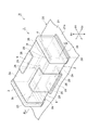
図1は、実施形態に係る積層貫通コンデンサを示す斜視図である。図2は、図1におけるII-II線に沿う断面図である。図1及び図2に示されるように、積層貫通コンデンサ1は、素体2と、一対の信号用端子電極3,4と、一対の接地用端子電極5,6と、複数の信号用内部電極11と、複数の接地用内部電極12と、を備えている。
(Multilayer feedthrough capacitor)
FIG. 1 is a perspective view illustrating the multilayer feedthrough capacitor according to the embodiment. FIG. 2 is a cross-sectional view taken along the line II-II in FIG. As shown in FIGS. 1 and 2, the
素体2は、直方体形状を呈している。直方体形状には、角部及び稜線部が面取りされている直方体の形状、及び、角部及び稜線部が丸められている直方体の形状が含まれる。素体2は、その外表面として、第一及び第二主面2a,2bと、第一〜第四側面2c〜2fとを有している。
The
第一及び第二主面2a,2bは、長方形状を呈し、互いに対向している。本実施形態では、第一及び第二主面2a,2bの対向方向を第一方向D1とし、第一及び第二主面2a,2bの長辺方向を第二方向D2とし、第一及び第二主面2a,2bの短辺方向を第三方向D3として説明を行う。第一〜第三方向D1〜D3は、互いに直交している。
The first and second
第一及び第二側面2c,2dは、矩形状を呈し、第二方向D2で互いに対向している。第一及び第二側面2c,2dは、第一及び第二主面2a,2b間を連結するように第三方向D3に延びている。第三及び第四側面2e,2fは、矩形状を呈し、第三方向D3で互いに対向している。第三及び第四側面2e,2fは、第一及び第二主面2a,2b間を連結するように第二方向D2に延びている。
The first and
素体2の第一方向D1での長さ(高さ)は、たとえば0.3mmである。素体2の第二方向D2での長さ(長さ)は、1.6mm以下であり、たとえば1.3mmである。素体2の第三方向D3での長さ(幅)は、たとえば0.5mmである。素体2の第二方向D2での長さは、第一及び第二主面2a,2bの長辺の長さに対応している。素体2の第三方向D3での長さは、第一及び第二主面2a,2bの短辺の長さに対応している。
The length (height) of the
素体2は、第一方向D1に複数の誘電体層が積層されて構成されている。各誘電体層は、たとえばBaTiO3、CaTiO3、SrTiO3、CaZrO3などの誘電体セラミックを含むセラミックグリーンシートの焼結体から構成されている。実際の素体2では、各誘電体層は、各誘電体層の間の境界が視認できない程度に一体化されている。
The
一対の信号用端子電極3,4は、互いに第二方向D2に離間している。信号用端子電極3は、素体2の第一側面2c側に配置されている。信号用端子電極3は、第一側面2cの全面を覆うように、第一及び第二主面2a,2b並びに第三及び第四側面2e,2fの端部(第一側面2c側の端部)にわたって配置されている。
The pair of
信号用端子電極4は、素体2の第二側面2d側に配置されている。信号用端子電極4は、第二側面2dの全面を覆うように、第一及び第二主面2a,2b並びに第三及び第四側面2e,2fの端部(第二側面2d側の端部)にわたって配置されている。
The
一対の接地用端子電極5,6は、互いに第三方向D3に離間している。接地用端子電極5は、素体2の第三側面2e側に配置されている。接地用端子電極5は、第三側面2eの第二方向D2の略中央を、第一方向D1に沿って横断するように覆っている。接地用端子電極5は、さらに第一及び第二主面2a,2bの第三側面2e側の端部の一部も覆っている。
The pair of
接地用端子電極6は、素体2の第四側面2f側に配置されている。接地用端子電極6は、第四側面2fの第二方向D2の略中央を、第一方向D1に沿って横断するように覆っている。接地用端子電極6は、さらに第一及び第二主面2a,2bの第四側面2f側の端部の一部も覆っている。
The
信号用内部電極11及び接地用内部電極12は、積層型の電気素子の内部電極として通常用いられる導電性材料(たとえばNi又はCuなど)からなる。信号用内部電極11及び接地用内部電極12は、上記導電性材料を含む導電性ペーストの焼結体として構成される。信号用内部電極11及び接地用内部電極12は、第一方向D1において異なる位置(層)に配置されている。すなわち、信号用内部電極11及び接地用内部電極12は、素体2内において、第一方向D1に間隔を有して対向するように交互に配置されている。
The signal
図3は、図2におけるIII-III線に沿う断面図である。図3に示されるように、信号用内部電極11は、第二方向D2を長辺方向とする長方形状を呈している。信号用内部電極11は、第一側面2cから第二側面2dまで延びている。信号用内部電極11は、一対の信号用端子電極3,4に接続されている。具体的には、信号用内部電極11の第一側面2c側の端部は、第一側面2cに露出し、信号用端子電極3に接続されている。信号用内部電極11の第二側面2d側の端部は、第二側面2dに露出し、信号用端子電極4に接続されている。信号用内部電極11は、第一及び第二主面2a,2b並びに第三及び第四側面2e,2fには露出していない。
3 is a cross-sectional view taken along line III-III in FIG. As shown in FIG. 3, the signal
図4は、図2におけるIV-IV線に沿う断面図である。図4に示されるように、接地用内部電極12は、主電極部12aと、一対の接続部12b,12cと、を有している。主電極部12aと、一対の接続部12b,12cとは、一体的に形成されている。主電極部12aは、第二方向D2を長辺方向とする長方形状を呈している。一対の接続部12b,12cは、例えば、互いに同じ矩形状を呈している。一対の接続部12b,12cは、主電極部12aを介して第三方向D3で互いに対向している。
4 is a cross-sectional view taken along line IV-IV in FIG. As shown in FIG. 4, the grounding
接続部12bは、主電極部12aの第三側面2e側の端部、かつ、第二方向D2の中央部から第三側面2eまで延びている。接続部12cは、主電極部12aの第四側面2f側の端部、かつ、第二方向D2の中央部から第四側面2fまで延びている。接地用内部電極12は、一対の接地用端子電極5,6に接続されている。具体的には、接続部12bの第三側面2e側の端部は、第三側面2eに露出し、接地用端子電極5に接続されている。接続部12cの第四側面2f側の端部は、第四側面2fに露出し、接地用端子電極6に接続されている。接地用内部電極12は、第一及び第二主面2a,2b並びに第一及び第二側面2c,2dには露出していない。
The
ここで、素体2の第二方向D2での長さをL、接地用内部電極12の接地用端子電極5,6に接続される接続部12b,12cの第二方向D2での長さをA、接地用端子電極5,6の第二方向D2での長さをCとしたとき、
L≦1.6mm
C/L≧0.40
A/L≧0.20
を満たしている。
Here, the length in the second direction D2 of the
L ≦ 1.6mm
C / L ≧ 0.40
A / L ≧ 0.20
Meet.
なお、接続部12b,12cが互いに同じ矩形状を呈し、接続部12b,12cの第二方向D2での長さが一つの値に決まる場合は、その値をAとすることができる。接続部12b,12cが互いに異なる形状を呈している場合、接続部12b,12cが矩形状以外の形状を呈している場合などのように、接続部12b,12cの第二方向D2での長さが一つの値に決まらない場合は、最小値をAとすることができる。
In addition, when the
続いて、実施例と比較例とによって、本実施形態では、低ESL化が図られていることを具体的に示す。実施例1〜5に係る積層貫通コンデンサとして、積層貫通コンデンサ1に対応するものを用いた。比較例1,2に係る積層貫通コンデンサとして、A/Lが0.20よりも小さく、C/Lが0.40よりも小さい点で、積層貫通コンデンサ1と異なるものを用いた。実施例1〜5及び比較例1,2に係る積層貫通コンデンサのL,A,A/L,C、及びC/Lの各値と、ESL測定結果と、判定結果とを表1に示す。
Subsequently, the embodiment and the comparative example specifically show that the ESL is reduced in this embodiment. As the multilayer feedthrough capacitor according to Examples 1 to 5, the one corresponding to the

判定結果は、比較例1に係る積層貫通コンデンサのESL値を基準値とし、ESL値が基準値の半分以下であれば「A」、ESL値が基準値の半分よりも大きければ「B」で示されている。表1に示されるように、実施例1〜5の判定結果はいずれも「A」である。すなわち、実施例1〜5では、ESLが基準値の半分以下となっている。 The determination result is “A” if the ESL value of the multilayer feedthrough capacitor according to Comparative Example 1 is a reference value, and “B” if the ESL value is greater than half the reference value. It is shown. As shown in Table 1, the determination results of Examples 1 to 5 are all “A”. That is, in Examples 1 to 5, ESL is less than half of the reference value.
以上説明したように、素体2の第二方向D2での長さが1.6mm以下であるとともに、接地用端子電極5,6の第二方向D2での長さが、素体2の第二方向D2での長さに対して0.40以上、かつ、接続部12b,12cの第二方向D2での長さが、素体2の第二方向D2での長さに対して0.20以上である。このように、積層貫通コンデンサ1では、素体2の第二方向D2の長さに対して、接地用端子電極5,6及び接続部12b,12cの第二方向D2での長さが、それぞれ所定値以上とされている。これにより、本実施形態では、素体2の第二方向D2での長さに対して、接地用端子電極5,6及び接続部12b,12cの第二方向D2での長さが、それぞれ所定値未満とされている場合に比べて、低ESL化が図られている。
As described above, the length of the
(電子部品装置)
図5は、実施形態に係る電子部品装置を示す斜視図である。図6は、図5におけるVI-VI線に沿う断面図である。図5及び図6に示されるように、電子部品装置10は、積層貫通コンデンサ1と、積層貫通コンデンサ1が実装された実装基板20と、を備えている。実装基板20は、基板本体21と、一対の信号用実装電極23,24と、一対の接地用実装電極25,26と、導体層27と、複数のビア導体28と、を有している。
(Electronic component equipment)
FIG. 5 is a perspective view showing the electronic component device according to the embodiment. 6 is a cross-sectional view taken along line VI-VI in FIG. As shown in FIGS. 5 and 6, the
基板本体21は、積層貫通コンデンサ1と対向する実装面21aを含んでいる。基板本体21は、たとえば、樹脂基板により構成されてもよいし、ガラスエポキシ基板などのフィラーを含む樹脂基板により構成されていてもよい。基板本体21の種類は特に限定されない。基板本体21は、導体層27を介して第一方向D1で互いに対向する第一及び第二絶縁体層31,32を含んでいる。第二絶縁体層32の一方の主面は、実装面21aである。第二絶縁体層32には、複数のビアホール29が形成されている。ビアホール29は、第二絶縁体層32を第一方向D1に貫通している。
The
一対の信号用実装電極23,24は、第二方向D2に離間して、実装面21aに配置されている。一対の信号用実装電極23,24は、第一方向D1から見て、矩形状を呈している。一対の信号用実装電極23,24の第二方向D2での長さは、たとえば0.3mmである。一対の信号用実装電極23,24の第三方向D3での長さは、0.5mm〜0.8mmであり、たとえば0.5mmである。
The pair of
信号用実装電極23は、信号用端子電極3に電気的に接続されている。信号用実装電極24は、信号用端子電極4に電気的に接続されている。一対の信号用実装電極23,24は、たとえば、はんだ、導電性樹脂などにより一対の信号用端子電極3,4に電気的に接続されている。
The
一対の接地用実装電極25,26は、第三方向D3に離間して、実装面21aに配置されている。一対の接地用実装電極25,26は、第一方向D1から見て、矩形状を呈している。一対の接地用実装電極25,26の第二方向D2での長さは、たとえば0.5mmであり、一対の接地用実装電極25,26の第三方向D3での長さは、たとえば0.3mmである。
The pair of
接地用実装電極25は、接地用端子電極5に電気的に接続されている。接地用実装電極26は、接地用端子電極6に電気的に接続されている。一対の接地用実装電極25,26は、たとえば、はんだ、導電性樹脂などにより一対の接地用端子電極5,6に電気的に接続されている。
The
導体層27は、第一絶縁体層31と第二絶縁体層32との間に配置されている。導体層27は、第二絶縁体層32を挟んで接地用実装電極25,26のそれぞれと第一方向D1で対向している。導体層27は、導電性材料(たとえばNi又はCuなど)からなる。導体層27は、たとえば、上記導電性材料を含む導電性ペーストの焼結体として構成される。
The
ビア導体28は、ビアホール29内に設けられている。ビア導体28は、たとえば、ビアホール29に導電性金属(たとえばCuなど)を無電界めっきにより成長させることによって形成される。ビア導体28は、接地用実装電極25,26と導体層27とに接続されている。本実施形態では、接地用実装電極25には2つのビア導体28が接続されており、当該2つのビア導体28は第二方向D2に並んでいる。また、接地用実装電極26には2つのビア導体28が接続されており、当該2つのビア導体28は第二方向D2に並んでいる。
The via
以上説明したように、電子部品装置10は、積層貫通コンデンサ1を備えている。これにより、低ESL化が図られている。
As described above, the
図7(a)は、実施形態に係る電子部品装置の平面図である。積層貫通コンデンサ1は、破線で示されている。図7(a)に示されるように、電子部品装置10では、ビア導体28が接地用実装電極25,26のそれぞれに2つずつ接続されており、ビア導体28の合計数が4つである。
FIG. 7A is a plan view of the electronic component device according to the embodiment. The
図7(b)は、比較形態に係る電子部品装置の平面図である。図7(b)では、比較形態に係る電子部品装置10Aを第二方向D2に2つ並べて配置した状態が示されている。図7(b)に示されるように、比較形態に係る電子部品装置10Aは、積層貫通コンデンサ1Aと、実装基板20Aとを備えている。ここでは、2つの電子部品装置10Aが1つの実装基板20Aを共有している。
FIG.7 (b) is a top view of the electronic component apparatus which concerns on a comparison form. FIG. 7B shows a state in which two
積層貫通コンデンサ1Aは、破線で示されている。積層貫通コンデンサ1Aは、主に、A/Lが0.20よりも小さく、C/Lが0.40よりも小さい点で、積層貫通コンデンサ1と相違している。実装基板20Aは、主に、接地用実装電極25,26の寸法の点で実装基板20と相違している。電子部品装置10Aでは、ビア導体28が接地用実装電極25,26のそれぞれに1つずつ接続されており、ビア導体28の合計数が2つである。
The
積層貫通コンデンサ1の第二方向D2での長さは、積層貫通コンデンサ1Aの第二方向D2での長さよりも長く、積層貫通コンデンサ1の容量は、積層貫通コンデンサ1Aの容量よりも大きい。仮に、積層貫通コンデンサ1の容量が、積層貫通コンデンサ1Aの容量の2倍であるとすると、積層貫通コンデンサ1を用いた場合は、積層貫通コンデンサ1Aを2つ用いた場合よりも、実装面積を削減させながら、積層貫通コンデンサ1Aを2つ用いた場合と同じ容量を維持することができる。
The length of the
実施例と比較例とによって、本実施形態の実装面積の削減効果を具体的に示す。実施例1,4〜6に係る電子部品装置として、それぞれ上述の実施例1,4〜6に係る積層貫通コンデンサを備え、電子部品装置10に対応するものを用いた。比較例1に係る電子部品装置として、上述の比較例1に係る積層貫通コンデンサを備え、電子部品装置10Aに対応するものを用いた。
The effect of reducing the mounting area of the present embodiment will be specifically shown by examples and comparative examples. As the electronic component devices according to Examples 1 and 4 to 6, devices corresponding to the
実施例1,4〜6及び比較例1に係る電子部品装置のビア導体の合計数と、実装面積削減率とを表2に示す。実装面積削減率は、比較例1に係る積層貫通コンデンサを2つ用いた場合の実装面積を基準として算出されている。2つの積層貫通コンデンサ間に所定の間隔を設ける必要があることから、基準となる実装面積は、比較例1に係る積層貫通コンデンサの実装面積を2倍したものよりも大きい。 Table 2 shows the total number of via conductors and the mounting area reduction rate of the electronic component devices according to Examples 1 and 4 to 6 and Comparative Example 1. The mounting area reduction rate is calculated on the basis of the mounting area when two multilayer feedthrough capacitors according to Comparative Example 1 are used. Since it is necessary to provide a predetermined interval between the two multilayer feedthrough capacitors, the reference mounting area is larger than twice the mounting area of the multilayer feedthrough capacitor according to Comparative Example 1.
表2に示されるように、実施例1,4〜6に係る電子部品装置では、実装面積が40%以上削減された。このように、本実施形態では、低ESL化が図られていることに加えて、実装面積が削減されている。 As shown in Table 2, in the electronic component devices according to Examples 1 and 4 to 6, the mounting area was reduced by 40% or more. Thus, in this embodiment, in addition to the reduction in ESL, the mounting area is reduced.
以上、本発明の実施形態について説明してきたが、本発明は必ずしも上述した実施形態に限定されるものではなく、その要旨を逸脱しない範囲で様々な変更が可能である。 As mentioned above, although embodiment of this invention has been described, this invention is not necessarily limited to embodiment mentioned above, A various change is possible in the range which does not deviate from the summary.
1…積層貫通コンデンサ、2…素体、2a…第一主面、2b…第二主面、2c…第一側面、2d…第二側面、2e…第三側面、2f…第四側面、3,4…信号用端子電極、5,6…接地用端子電極、11…信号用内部電極、12…接地用内部電極、12b,12c…接続部、20…実装基板、21…基板本体、21a…実装面、23,24…信号用実装電極、24,25…接地用実装電極、27…導体層、28…ビア導体、32…第二絶縁体層。
DESCRIPTION OF
Claims (2)
前記素体の前記第一及び第二側面側に配置された一対の信号用端子電極と、
前記素体の前記第三及び第四側面側に配置された一対の接地用端子電極と、
前記素体内に前記第一及び第二主面の対向方向に交互に配置された、それぞれ複数の信号用内部電極及び接地用内部電極と、を備え、
各前記信号用内部電極は、前記一対の信号用端子電極に接続され、
各前記接地用内部電極は、前記一対の接地用端子電極に接続され、
前記素体の前記長辺方向での長さをL、前記接地用内部電極の前記接地用端子電極に接続される接続部の前記長辺方向での長さをA、前記接地用端子電極の前記長辺方向での長さをCとしたとき、
L≦1.6mm
C/L≧0.40
A/L≧0.20
を満たしている、積層貫通コンデンサ。 A rectangular first and second main surfaces that face each other, and a first side that extends in the short side direction of the first and second main surfaces so as to connect the first and second main surfaces and that face each other. One and second side surfaces, and third and fourth side surfaces extending in the long side direction of the first and second main surfaces so as to connect the first and second main surfaces and facing each other. An element body,
A pair of signal terminal electrodes disposed on the first and second side surfaces of the element body;
A pair of grounding terminal electrodes disposed on the third and fourth side surfaces of the element body;
A plurality of signal internal electrodes and ground internal electrodes, which are alternately arranged in the element body in the opposing direction of the first and second main surfaces,
Each of the signal internal electrodes is connected to the pair of signal terminal electrodes,
Each of the grounding internal electrodes is connected to the pair of grounding terminal electrodes,
The length of the element body in the long side direction is L, the length of the connecting portion connected to the grounding terminal electrode of the grounding internal electrode is A, and the length of the grounding terminal electrode is When the length in the long side direction is C,
L ≦ 1.6mm
C / L ≧ 0.40
A / L ≧ 0.20
Meets the multilayer feedthrough capacitor.
前記積層貫通コンデンサが実装された実装基板と、を備え、
前記実装基板は、
前記積層貫通コンデンサと対向する実装面を含む基板本体と、
前記実装面に配置され、かつ、前記一対の信号用端子電極に電気的に接続された一対の信号用実装電極と、
互いに離間して前記実装面に配置され、かつ、前記一対の接地用端子電極に電気的に接続された一対の接地用実装電極と、
前記基板本体の少なくとも一部を挟んで各前記接地用実装電極と対向する導体部と、
各前記接地用実装電極と前記導体部とに接続された複数のビア導体と、を有する、電子部品装置。
A multilayer feedthrough capacitor according to claim 1;
A mounting substrate on which the multilayer feedthrough capacitor is mounted,
The mounting substrate is
A substrate body including a mounting surface facing the multilayer feedthrough capacitor;
A pair of signal mounting electrodes disposed on the mounting surface and electrically connected to the pair of signal terminal electrodes;
A pair of grounding mounting electrodes disposed on the mounting surface apart from each other and electrically connected to the pair of grounding terminal electrodes;
A conductor portion facing each grounding mounting electrode across at least a portion of the substrate body;
An electronic component device comprising: a plurality of via conductors connected to each of the grounding mounting electrodes and the conductor portion.
Priority Applications (1)
| Application Number | Priority Date | Filing Date | Title |
|---|---|---|---|
| JP2016020649A JP2017139403A (en) | 2016-02-05 | 2016-02-05 | Multilayer penetration capacitor and electronic component device |
Applications Claiming Priority (1)
| Application Number | Priority Date | Filing Date | Title |
|---|---|---|---|
| JP2016020649A JP2017139403A (en) | 2016-02-05 | 2016-02-05 | Multilayer penetration capacitor and electronic component device |
Publications (1)
| Publication Number | Publication Date |
|---|---|
| JP2017139403A true JP2017139403A (en) | 2017-08-10 |
Family
ID=59566911
Family Applications (1)
| Application Number | Title | Priority Date | Filing Date |
|---|---|---|---|
| JP2016020649A Pending JP2017139403A (en) | 2016-02-05 | 2016-02-05 | Multilayer penetration capacitor and electronic component device |
Country Status (1)
| Country | Link |
|---|---|
| JP (1) | JP2017139403A (en) |
Cited By (2)
| Publication number | Priority date | Publication date | Assignee | Title |
|---|---|---|---|---|
| JP2019062023A (en) * | 2017-09-25 | 2019-04-18 | Tdk株式会社 | Electronic component device |
| JP7342802B2 (en) | 2020-06-11 | 2023-09-12 | Tdk株式会社 | Mounting structure of semiconductor ceramic electronic components |
Citations (3)
| Publication number | Priority date | Publication date | Assignee | Title |
|---|---|---|---|---|
| JP2011097091A (en) * | 2007-02-05 | 2011-05-12 | Samsung Electro-Mechanics Co Ltd | Laminated chip capacitor |
| JP2015019084A (en) * | 2014-08-13 | 2015-01-29 | 株式会社村田製作所 | Capacitor and mounting structure of capacitor |
| JP2017117865A (en) * | 2015-12-22 | 2017-06-29 | 株式会社村田製作所 | Capacitor and capacitor built-in substrate |
-
2016
- 2016-02-05 JP JP2016020649A patent/JP2017139403A/en active Pending
Patent Citations (3)
| Publication number | Priority date | Publication date | Assignee | Title |
|---|---|---|---|---|
| JP2011097091A (en) * | 2007-02-05 | 2011-05-12 | Samsung Electro-Mechanics Co Ltd | Laminated chip capacitor |
| JP2015019084A (en) * | 2014-08-13 | 2015-01-29 | 株式会社村田製作所 | Capacitor and mounting structure of capacitor |
| JP2017117865A (en) * | 2015-12-22 | 2017-06-29 | 株式会社村田製作所 | Capacitor and capacitor built-in substrate |
Non-Patent Citations (1)
| Title |
|---|
| "EMIFIL(Capacitor type) Single Circuit Type for Large Current NFM15PC Series(0402 Size)", [ONLINE], JPN6019028426, 8 September 2014 (2014-09-08), ISSN: 0004226102 * |
Cited By (2)
| Publication number | Priority date | Publication date | Assignee | Title |
|---|---|---|---|---|
| JP2019062023A (en) * | 2017-09-25 | 2019-04-18 | Tdk株式会社 | Electronic component device |
| JP7342802B2 (en) | 2020-06-11 | 2023-09-12 | Tdk株式会社 | Mounting structure of semiconductor ceramic electronic components |
Similar Documents
| Publication | Publication Date | Title |
|---|---|---|
| US9892855B2 (en) | Electronic component | |
| JP2017073434A (en) | Electronic component | |
| US8526162B2 (en) | Feedthrough multilayer capacitor | |
| KR101020528B1 (en) | Multilayer condenser | |
| KR20080008979A (en) | Feedthrough multilayer capacitor | |
| KR101051620B1 (en) | Multilayer capacitor | |
| US8395881B2 (en) | Multilayer feedthrough capacitor and mounted structure of multilayer feedthrough capacitor | |
| US10650972B2 (en) | Electronic component | |
| US7535694B2 (en) | Feedthrough multilayer capacitor | |
| US10755861B2 (en) | Electronic component | |
| KR20170113280A (en) | Multilayer capacitor | |
| US10395844B2 (en) | Capacitor component | |
| JP2014183241A (en) | Penetration type capacitor | |
| JP2017139403A (en) | Multilayer penetration capacitor and electronic component device | |
| JP5042892B2 (en) | Feedthrough capacitor | |
| JP6459717B2 (en) | Multilayer ceramic capacitor | |
| JP5741416B2 (en) | Electronic component mounting structure | |
| JP6662229B2 (en) | Multilayer feedthrough capacitors and electronic component devices | |
| JP2016149425A (en) | Stack penetration capacitor | |
| JP5929524B2 (en) | Multilayer capacitor | |
| CN111261366B (en) | Laminated coil component | |
| US11373807B2 (en) | Electronic component device | |
| JP6919455B2 (en) | Electronic component equipment | |
| JP2016136562A (en) | Multilayer capacitor | |
| JP2010124010A (en) | Feedthrough capacitor |
Legal Events
| Date | Code | Title | Description |
|---|---|---|---|
| A621 | Written request for application examination |
Free format text: JAPANESE INTERMEDIATE CODE: A621 Effective date: 20181012 |
|
| A977 | Report on retrieval |
Free format text: JAPANESE INTERMEDIATE CODE: A971007 Effective date: 20190717 |
|
| A131 | Notification of reasons for refusal |
Free format text: JAPANESE INTERMEDIATE CODE: A131 Effective date: 20190730 |
|
| A02 | Decision of refusal |
Free format text: JAPANESE INTERMEDIATE CODE: A02 Effective date: 20200310 |