JP2017123732A - Driving circuit of semiconductor device - Google Patents
Driving circuit of semiconductor device Download PDFInfo
- Publication number
- JP2017123732A JP2017123732A JP2016001772A JP2016001772A JP2017123732A JP 2017123732 A JP2017123732 A JP 2017123732A JP 2016001772 A JP2016001772 A JP 2016001772A JP 2016001772 A JP2016001772 A JP 2016001772A JP 2017123732 A JP2017123732 A JP 2017123732A
- Authority
- JP
- Japan
- Prior art keywords
- gate
- semiconductor element
- circuit
- resistor
- delay circuit
- Prior art date
- Legal status (The legal status is an assumption and is not a legal conclusion. Google has not performed a legal analysis and makes no representation as to the accuracy of the status listed.)
- Pending
Links
- 239000004065 semiconductor Substances 0.000 title claims abstract description 137
- 230000003111 delayed effect Effects 0.000 claims abstract description 13
- 239000003990 capacitor Substances 0.000 claims description 22
- 238000010586 diagram Methods 0.000 description 10
- XUIMIQQOPSSXEZ-UHFFFAOYSA-N Silicon Chemical compound [Si] XUIMIQQOPSSXEZ-UHFFFAOYSA-N 0.000 description 4
- 238000006243 chemical reaction Methods 0.000 description 4
- 239000000463 material Substances 0.000 description 4
- 230000004048 modification Effects 0.000 description 4
- 238000012986 modification Methods 0.000 description 4
- 238000010248 power generation Methods 0.000 description 4
- 229910052710 silicon Inorganic materials 0.000 description 4
- 239000010703 silicon Substances 0.000 description 4
- 230000001133 acceleration Effects 0.000 description 3
- 238000007599 discharging Methods 0.000 description 3
- 229910002601 GaN Inorganic materials 0.000 description 2
- JMASRVWKEDWRBT-UHFFFAOYSA-N Gallium nitride Chemical compound [Ga]#N JMASRVWKEDWRBT-UHFFFAOYSA-N 0.000 description 2
- 230000001934 delay Effects 0.000 description 2
- 238000001514 detection method Methods 0.000 description 2
- HBMJWWWQQXIZIP-UHFFFAOYSA-N silicon carbide Chemical compound [Si+]#[C-] HBMJWWWQQXIZIP-UHFFFAOYSA-N 0.000 description 2
- 229910010271 silicon carbide Inorganic materials 0.000 description 2
- 239000000758 substrate Substances 0.000 description 2
- 229910003460 diamond Inorganic materials 0.000 description 1
- 239000010432 diamond Substances 0.000 description 1
- AJNVQOSZGJRYEI-UHFFFAOYSA-N digallium;oxygen(2-) Chemical compound [O-2].[O-2].[O-2].[Ga+3].[Ga+3] AJNVQOSZGJRYEI-UHFFFAOYSA-N 0.000 description 1
- 230000000694 effects Effects 0.000 description 1
- 230000005669 field effect Effects 0.000 description 1
- 229910044991 metal oxide Inorganic materials 0.000 description 1
- 150000004706 metal oxides Chemical class 0.000 description 1
- 238000012544 monitoring process Methods 0.000 description 1
Images
Landscapes
- Power Conversion In General (AREA)
Abstract
Description
本発明は、半導体素子の駆動回路に関する。 The present invention relates to a drive circuit for a semiconductor element.
モータ駆動装置、発電装置、電動コンプレッサ、電力変換装置(コンバータ、インバータ)等の装置では、電力制御を行うために半導体素子が用いられている。例えば、MOSFET(Metal Oxide Semiconductor Field Effect Transistor:電界効果トランジスタ)、IGBT(Insulated Gate Bipolar Transistor:絶縁ゲートバイポーラトランジスタ)等の電圧駆動型の電力用半導体素子が用いられている。 In devices such as a motor drive device, a power generation device, an electric compressor, and a power conversion device (converter, inverter), a semiconductor element is used for power control. For example, voltage-driven power semiconductor elements such as MOSFETs (Metal Oxide Semiconductor Field Effect Transistors) and IGBTs (Insulated Gate Bipolar Transistors) are used.
このような半導体素子では、ターンオン動作時に生ずる急激な電流変化が原因で、サージ電圧やノイズが発生することがある。このサージ電圧やノイズを抑制するには、半導体素子のスイッチング速度を遅くして、ターンオン動作中に半導体素子を流れる電流の時間変化率を小さくすることが有効である。しかしながら、半導体素子のスイッチング速度を遅くすると、ターンオン動作中のスイッチング損失が増えてしまう。このように、「サージ電圧やノイズを抑制すること」と「スイッチング損失を抑制すること」とはトレードオフの関係にある。 In such a semiconductor element, a surge voltage or noise may occur due to a rapid current change that occurs during the turn-on operation. In order to suppress the surge voltage and noise, it is effective to reduce the time change rate of the current flowing through the semiconductor element during the turn-on operation by reducing the switching speed of the semiconductor element. However, when the switching speed of the semiconductor element is slowed, the switching loss during the turn-on operation increases. Thus, “suppressing surge voltage and noise” and “suppressing switching loss” are in a trade-off relationship.
以下の特許文献1〜5には、従来の半導体素子の駆動回路の一例が開示されている。例えば、以下の特許文献1には、IGBTのターンオン動作中に、ゲート電圧を低い電位から高い電位に切り替えることで、サージ電圧やノイズを抑制しつつスイッチング損失を抑制する駆動回路が開示されている。また、以下の特許文献5には、ターンオン動作中にMOSFETのゲート抵抗値を小さくすることで、ターンオン特性を改善する駆動回路が開示されている。
ところで、上述した特許文献1に開示された駆動回路は、ゲート電圧の切り替えを行うことでサージ電圧やノイズを抑制しつつスイッチング損失を抑制しているが、ゲート電圧の切り替えは、サージ電流が収まってから行う必要がある。このため、上述した特許文献1では、IGBTの入力電圧(コレクタ電圧)をモニタするモニタ回路、入力電圧の時間変化率から急峻な電流変化を検出する検出回路等が必要となり、駆動回路の回路規模が大きくなってしまうという問題がある。
By the way, the drive circuit disclosed in
また、上述した特許文献5に開示された駆動回路は、ターンオン動作中にMOSFETのゲート抵抗値を小さくすることによって、ターンオン特性を改善することが可能であるものの、更なる安定性の向上を図ることができる余地があると考えられる。半導体素子を安定して駆動することができれば、上述したモータ駆動装置、発電装置、電動コンプレッサ、電力変換装置(コンバータ、インバータ)等の装置の安定動作に繋がることになるため、安定性の向上は極めて重要である。 Further, although the drive circuit disclosed in Patent Document 5 described above can improve the turn-on characteristics by reducing the gate resistance value of the MOSFET during the turn-on operation, it further improves the stability. There seems to be room for it. If the semiconductor element can be driven stably, it will lead to stable operation of devices such as the motor drive device, power generation device, electric compressor, and power conversion device (converter, inverter) described above. Very important.
本発明は、上記事情に鑑みてなされたものであり、簡易な回路構成によって半導体素子を安定して駆動することが可能な半導体素子の駆動回路を提供することを目的とする。 The present invention has been made in view of the above circumstances, and an object of the present invention is to provide a semiconductor element driving circuit capable of stably driving a semiconductor element with a simple circuit configuration.
上記課題を解決するために、本発明の半導体素子の駆動回路は、半導体素子(Q1)の制御電極(G)に一端が接続された第1抵抗部(Rg1)と、半導体素子のオン状態を指令する指令信号に基づいてオン状態になり、電源(Vcc)と前記第1抵抗部の他端とを接続する第1スイッチ素子(Q2)とを備える半導体素子の駆動回路(1、2)において、前記指令信号を予め規定された時間だけ遅延させる遅延回路(13、23)と、前記遅延回路で遅延された前記指令信号に基づいて、前記電源と前記制御電極とを接続する第2スイッチ素子(Q4、Q5)と、を備える。
本発明の第1の態様による半導体素子の駆動回路は、前記第2スイッチ素子が、前記遅延回路で遅延された前記指令信号がゲートに入力されるpチャネルMOSFETであり、前記指令信号の論理を反転させて前記遅延回路に出力する反転回路(12)を備える。
また、本発明の第1の態様による半導体素子の駆動回路は、前記遅延回路が、前記反転回路と前記pチャネルMOSFETのゲートとの間に直列接続された抵抗(R1)と、前記pチャネルMOSFETのゲートとソースとの間に接続されたコンデンサ(C1)と、を備える。
本発明の第2の態様による半導体素子の駆動回路は、前記第2スイッチ素子が、前記遅延回路で遅延された前記指令信号がゲートに入力されるnチャネルMOSFETである。
本発明の第2の態様による半導体素子の駆動回路は、前記遅延回路が、一端が前記nチャネルMOSFETのゲートに接続され、他端に前記指令信号が入力される抵抗(R2)と、一端が前記nチャネルMOSFETのゲートに接続され、他端が接地されたコンデンサ(C2)と、を備える。
また、本発明の半導体素子の駆動回路は、前記第2スイッチ素子と前記制御電極との間に直列接続された第2抵抗部(Rg3、Rg4)を備える。
In order to solve the above-described problems, a semiconductor element driving circuit according to the present invention includes a first resistance portion (Rg1) having one end connected to a control electrode (G) of a semiconductor element (Q1), and an on-state of the semiconductor element. In a drive circuit (1, 2) for a semiconductor element that is turned on based on a command signal to be commanded and includes a power switch (Vcc) and a first switch element (Q2) that connects the other end of the first resistor section. A delay circuit (13, 23) for delaying the command signal by a predetermined time, and a second switch element for connecting the power source and the control electrode based on the command signal delayed by the delay circuit (Q4, Q5).
In the semiconductor element driving circuit according to the first aspect of the present invention, the second switch element is a p-channel MOSFET in which the command signal delayed by the delay circuit is input to a gate, and the logic of the command signal is determined. An inverting circuit (12) for inverting and outputting to the delay circuit is provided.
In the semiconductor element drive circuit according to the first aspect of the present invention, the delay circuit includes a resistor (R1) connected in series between the inverting circuit and the gate of the p-channel MOSFET, and the p-channel MOSFET. And a capacitor (C1) connected between the gate and the source.
In the semiconductor element driving circuit according to the second aspect of the present invention, the second switch element is an n-channel MOSFET in which the command signal delayed by the delay circuit is input to a gate.
In the semiconductor element driving circuit according to the second aspect of the present invention, the delay circuit includes a resistor (R2) having one end connected to the gate of the n-channel MOSFET and the other end receiving the command signal, and one end A capacitor (C2) connected to the gate of the n-channel MOSFET and grounded at the other end.
In addition, the semiconductor element drive circuit of the present invention includes a second resistance portion (Rg3, Rg4) connected in series between the second switch element and the control electrode.
本発明によれば、半導体素子のオン状態を指令する指令信号を遅延回路で予め規定された時間だけ遅延させ、遅延回路で遅延された指令信号に基づいて、電源と制御電極とを第2スイッチ素子によって接続するようにしているため、簡易な回路構成によって半導体素子を安定して駆動することが可能であるという効果がある。 According to the present invention, the command signal for commanding the ON state of the semiconductor element is delayed by a predetermined time by the delay circuit, and the power source and the control electrode are connected to the second switch based on the command signal delayed by the delay circuit. Since the connection is made by the elements, there is an effect that the semiconductor elements can be stably driven by a simple circuit configuration.
以下、図面を参照して本発明の実施形態による半導体素子の駆動回路について詳細に説明する。 Hereinafter, a driving circuit of a semiconductor device according to an embodiment of the present invention will be described in detail with reference to the drawings.
〔第1実施形態〕
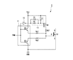
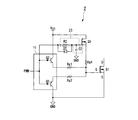
図1は、本発明の第1実施形態による半導体素子の駆動回路の構成を示す回路図である。図1に示す通り、本実施形態の駆動回路1は、増幅部11、ゲート抵抗Rg1(第1抵抗部)、ゲート抵抗Rg2、ゲート抵抗Rg3(第2抵抗部)、スイッチング用MOSFETQ4(第2スイッチ素子)、反転回路12、遅延回路13、及びダイオードD1を備えており、外部から入力されるPWM(Pulse Width Modulation:パルス幅変調)信号に基づいて半導体素子Q1を駆動する回路である。
[First Embodiment]
FIG. 1 is a circuit diagram showing a configuration of a drive circuit for a semiconductor device according to a first embodiment of the present invention. As shown in FIG. 1, the
ここで、駆動対象である半導体素子Q1は、電圧駆動型の電力用半導体素子であり、例えばシリコンよりもバンドギャップが大きい半導体材料を基板に含むワイドバンドギャップのパワーMOSFETである。シリコンよりもバンドギャップが大きい半導体材料としては、例えばSiC(シリコンカーバイド)、GaN(窒化ガリウム)、酸化ガリウム(Ga2O3)、ダイヤモンド半導体等が挙げられる。 Here, the semiconductor element Q1 to be driven is a voltage-driven power semiconductor element, for example, a wide-bandgap power MOSFET including a semiconductor material having a larger bandgap than silicon in a substrate. Examples of the semiconductor material having a band gap larger than that of silicon include SiC (silicon carbide), GaN (gallium nitride), gallium oxide (Ga 2 O 3 ), diamond semiconductor, and the like.
増幅部11は、NPNトランジスタQ2(第1スイッチ素子)とPNPトランジスタQ3とを備えており、半導体素子Q1のターンオン及びターンオフを制御するために、外部から入力されるPWM信号(指令信号)を増幅する。尚、以下では、説明を簡単にするために、NPNトランジスタQ2を「トランジスタQ2」と略記し、PNPトランジスタQ3を「トランジスタQ3」と略記する。
The amplifying
トランジスタQ2,Q3のベースは共通接続されており、各々のベースには外部からのPWM信号が入力される。トランジスタQ2のコレクタは電源Vccに接続されており、エミッタはゲート抵抗Rg1に接続されている。トランジスタQ3のコレクタは接地されており、エミッタはゲート抵抗Rg2に接続されている。トランジスタQ2は、半導体素子Q1のターンオンに対応するPWM信号のオン期間中に導通し(オン状態になり)、トランジスタQ3は、半導体素子Q1のターンオフに対応するPWM信号のオフ期間中に導通する(オン状態になる)。 The bases of the transistors Q2 and Q3 are connected in common, and an external PWM signal is input to each base. The collector of the transistor Q2 is connected to the power supply Vcc, and the emitter is connected to the gate resistor Rg1. The collector of the transistor Q3 is grounded, and the emitter is connected to the gate resistor Rg2. The transistor Q2 becomes conductive during the ON period of the PWM signal corresponding to the turn-on of the semiconductor element Q1 (becomes on), and the transistor Q3 becomes conductive during the OFF period of the PWM signal corresponding to the turn-off of the semiconductor element Q1 ( Will be on).
ゲート抵抗Rg1は、一端が半導体素子Q1のゲートG(制御電極)に接続されており、他端がトランジスタQ2のエミッタに接続されている。従って、トランジスタQ2の導通時には、ゲート抵抗Rg1を流れる電源Vccからのゲート電流によって、半導体素子Q1のゲートGが充電される。トランジスタQ2の導通時におけるゲート電流は、ゲート抵抗Rg1の抵抗値に応じた大きさである。 One end of the gate resistor Rg1 is connected to the gate G (control electrode) of the semiconductor element Q1, and the other end is connected to the emitter of the transistor Q2. Therefore, when the transistor Q2 is turned on, the gate G of the semiconductor element Q1 is charged by the gate current from the power source Vcc flowing through the gate resistor Rg1. The gate current when the transistor Q2 is conductive has a magnitude corresponding to the resistance value of the gate resistor Rg1.
ゲート抵抗Rg2は、一端が半導体素子Q1のゲートGに接続されており、他端がトランジスタQ3のエミッタに接続されている。従って、トランジスタQ3の導通時には、半導体素子Q1のゲートGに充電された電荷が、ゲート抵抗Rg2を介して放電される。電荷の放電に要する時間(放電速度)は、ゲート抵抗Rg2の抵抗値に応じて調整可能である。 One end of the gate resistor Rg2 is connected to the gate G of the semiconductor element Q1, and the other end is connected to the emitter of the transistor Q3. Therefore, when the transistor Q3 is turned on, the charge charged in the gate G of the semiconductor element Q1 is discharged through the gate resistor Rg2. The time required for discharging the charge (discharge rate) can be adjusted according to the resistance value of the gate resistor Rg2.
ゲート抵抗Rg3は、一端が半導体素子Q1のゲートGに接続されており、他端がスイッチング用MOSFETQ4のドレインに接続されている。ゲート抵抗Rg3の抵抗値は、ゲート抵抗Rg1との合成抵抗(ゲート抵抗Rg1,Rg3が並列接続された状態の合成抵抗)が、ゲート抵抗Rg1の抵抗値よりも十分に小さくなるように設定される。これは、半導体素子Q1のターンオン特性を改善するためである。 One end of the gate resistor Rg3 is connected to the gate G of the semiconductor element Q1, and the other end is connected to the drain of the switching MOSFET Q4. The resistance value of the gate resistance Rg3 is set so that the combined resistance with the gate resistance Rg1 (the combined resistance in a state where the gate resistances Rg1 and Rg3 are connected in parallel) is sufficiently smaller than the resistance value of the gate resistance Rg1. . This is to improve the turn-on characteristics of the semiconductor element Q1.
スイッチング用MOSFETQ4は、pチャネルMOSFETであり、ゲートが遅延回路13の出力端に接続されており、ドレインがゲート抵抗Rg3の他端に接続されており、ソースが電源Vccに接続されている。従って、スイッチング用MOSFETQ4の導通時には、ゲート抵抗Rg3を流れる電源Vccからのゲート電流によって、半導体素子Q1のゲートGが充電される。スイッチング用MOSFETQ4の導通時におけるゲート電流は、ゲート抵抗Rg3の抵抗値に応じた大きさである。
The switching MOSFET Q4 is a p-channel MOSFET, the gate is connected to the output terminal of the
反転回路12は、外部から入力されるPWM信号の論理を反転する回路である。具体的に、反転回路12は、PWM信号がHighレベル(Q1オン指令)の期間中は、Lowレベルとなる信号を出力し、PWM信号がLowレベル(Q1オフ指令)の期間中は、Highレベルとなる信号を出力する。この反転回路12は、入力端がトランジスタQ2,Q3のベースに接続されており、出力端が遅延回路13の入力端に接続されている。このため、反転回路12から出力される信号(PWM信号の論理を反転した信号)は、遅延回路13の入力端に入力される。
The inverting
遅延回路13は、抵抗R1及びコンデンサC1を備えており、反転回路12から出力される信号(PWM信号の論理を反転した信号)を、予め規定された時間だけ遅延させる。抵抗R1は、反転回路12の出力端と、スイッチング用MOSFETQ4のゲートとの間に直列接続されている。コンデンサC1は、スイッチング用MOSFETQ4のゲートとソースとの間に接続されている。
The
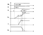
遅延回路13のコンデンサC1は、PWM信号がHighレベル(Q1オン指令)である場合(反転回路12から出力される信号がLowレベルである場合)に、電源Vccからの電流によって充電される。このコンデンサC1は、コンデンサC1及び抵抗R1で定まる遅延回路13の時定数に応じた遅延時間(t2−t1)をかけて充電される(図2参照)。コンデンサC1の充電電圧(ゲート電圧)が閾値を超えると、スイッチング用MOSFETQ4がオン状態になる。このように、スイッチング用MOSFETQ4は、PWM信号がオンになった時点から、遅延回路13の時定数に応じた遅延時間(t2−t1)だけ遅延したタイミングでオン状態になる。
The capacitor C1 of the
ここで、遅延回路13の時定数は、半導体素子Q1のターンオン動作中における急峻なドレイン電流Idの変化が、遅延回路13による遅延時間(t2−t1)内において生ずるように設定される。つまり、遅延回路13の時定数は、半導体素子Q1のターンオン指令が入力されてから(時刻t1)、半導体素子Q1のターンオン動作中における急峻なドレイン電流Idの変化が生じた後に、遅延回路13の遅延が終了する時刻t2が到来するように設定される。
Here, the time constant of the
ダイオードD1は、半導体素子Q1のターンオフ動作中に、コンデンサC1に充電された電荷を素早く放電するためのものであり、遅延回路13に設けられた抵抗R1に対して並列に接続されている。具体的に、ダイオードD1のアノードは、抵抗R1と反転回路12の出力端との接続点に接続され、カソードは、抵抗R1とコンデンサC1との接続点に接続されている。
The diode D1 is for quickly discharging the charge charged in the capacitor C1 during the turn-off operation of the semiconductor element Q1, and is connected in parallel to the resistor R1 provided in the
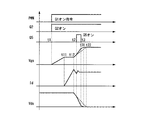
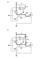
次に、上記構成における駆動回路1の動作について説明する。図2は、本発明の第1実施形態による半導体素子の駆動回路の動作を説明するためのタイミングチャートである。また、図3は、本発明の第1実施形態におけるゲート電流の経路を示す図である。図2に示す通り、時刻t1においてPWM信号がHighレベルになって半導体素子Q1のターンオン指令が駆動回路1に入力されるものとする。
Next, the operation of the
半導体素子Q1のターンオン指令が入力されると、増幅部11に設けられたトランジスタQ2がオン状態になる。すると、図3(a)に示す電流経路CP1を介してゲート電流が流れ、このゲート電流によって半導体素子Q1のゲートGが充電される。これにより、図2に示す通り、半導体素子Q1のゲート電圧Vgs(ゲートGとソースSとの間の電位差)が上昇する。尚、図3(a)に示す電流経路CP1は、電源VccからトランジスタQ2及びゲート抵抗Rg1を順に介して半導体素子Q1のゲートGに至る経路である。
When a turn-on command for the semiconductor element Q1 is input, the transistor Q2 provided in the amplifying
ゲート電圧Vgsが徐々に上昇していくと、半導体素子Q1のゲートGにチャネルが形成され始め、チャネルの厚みがある程度の厚みになると、半導体素子Q1のソースSとドレインDとの間にドレイン電流Idが流れ始める(図2中の時刻t11)。そして、図2に示す通り、ドレイン電流Idは、時刻t12になるまで時間の経過とともに上昇する。尚、図2に示す通り、半導体素子Q1のドレイン電圧Vds(ソースSとドレインDとの間の電位差)は、時刻t12までは一定の値である。 When the gate voltage Vgs gradually increases, a channel starts to be formed in the gate G of the semiconductor element Q1, and when the channel thickness reaches a certain thickness, the drain current flows between the source S and the drain D of the semiconductor element Q1. Id starts to flow (time t11 in FIG. 2). Then, as shown in FIG. 2, the drain current Id increases with time until time t12 is reached. As shown in FIG. 2, the drain voltage Vds (potential difference between the source S and the drain D) of the semiconductor element Q1 is a constant value until time t12.
また、半導体素子Q1のターンオン指令が入力されると(時刻t1)、反転回路12から遅延回路13に出力される信号はLowレベルとなる。すると、電源Vccからの電流によって、遅延回路13のコンデンサC1の充電が開始され、スイッチング用MOSFETQ4のゲート電圧が低下する。尚、コンデンサC1は、コンデンサC1及び抵抗R1によって定まる遅延回路13の時定数に応じた遅延時間(t2−t1)をかけて充電される。
When a turn-on command for the semiconductor element Q1 is input (time t1), the signal output from the inverting
PWM信号がHighレベル(Q1オン指令)になった時点から上記の遅延時間(t2−t1)が経過すると(時刻t2になると)、図2に示す通り、スイッチング用MOSFETQ4のゲート電圧が閾値を超えてオン状態になる。スイッチング用MOSFETQ4がオン状態になると、ゲート抵抗Rg3がゲート抵抗Rg1と並列接続された状態になる。これにより、半導体素子Q1のゲート抵抗の抵抗値は、ゲート抵抗Rg1の抵抗値から、ゲート抵抗Rg1とゲート抵抗Rg3とが並列接続された抵抗値(ゲート抵抗Rg1の抵抗値よりも小さな抵抗値)に切り替わる。 When the above delay time (t2-t1) elapses from the time when the PWM signal becomes High level (Q1 ON command) (at time t2), the gate voltage of the switching MOSFET Q4 exceeds the threshold value as shown in FIG. Turn on. When the switching MOSFET Q4 is turned on, the gate resistor Rg3 is connected in parallel with the gate resistor Rg1. Thereby, the resistance value of the gate resistance of the semiconductor element Q1 is the resistance value in which the gate resistance Rg1 and the gate resistance Rg3 are connected in parallel from the resistance value of the gate resistance Rg1 (resistance value smaller than the resistance value of the gate resistance Rg1). Switch to
すると、図3(b)に示す通り、電流経路CP1に加えて電流経路CP2を介してゲート電流が流れ、これら電流経路CP1,CP2を介するゲート電流によって半導体素子Q1のゲートGが充電される。尚、図3(b)に示す電流経路CP2は、電源Vccからスイッチング用MOSFETQ4及びゲート抵抗Rg3を順に介して半導体素子Q1のゲートGに至る経路である。 Then, as shown in FIG. 3B, a gate current flows through the current path CP2 in addition to the current path CP1, and the gate G of the semiconductor element Q1 is charged by the gate current through the current paths CP1 and CP2. A current path CP2 shown in FIG. 3B is a path from the power source Vcc to the gate G of the semiconductor element Q1 through the switching MOSFET Q4 and the gate resistor Rg3 in this order.
これにより、図2に示す通り、半導体素子Q1のゲート電圧Vgsの時間変化率が、ゲート抵抗の抵抗値が切り替わらない場合(点線で示す場合)に比べて高くなる。その結果、ゲート電圧Vgsがピーク値に達するタイミングが、ゲート抵抗の抵抗値が切り替わらない場合の時刻t22よりも早い時刻t21になる。つまり、時刻t2以降は、半導体素子Q1のターンオン動作が加速される。 As a result, as shown in FIG. 2, the time change rate of the gate voltage Vgs of the semiconductor element Q1 becomes higher than when the resistance value of the gate resistance is not switched (indicated by a dotted line). As a result, the timing at which the gate voltage Vgs reaches the peak value is a time t21 that is earlier than the time t22 when the resistance value of the gate resistance is not switched. That is, after time t2, the turn-on operation of the semiconductor element Q1 is accelerated.
尚、図2に示す通り、半導体素子Q1のドレイン電圧Vdsの時間変化率も、半導体素子Q1のゲート電圧Vgsと同様に、ゲート抵抗の抵抗値が切り替わらない場合(点線で示す場合)に比べて高くなる。その結果、ドレイン電圧Vdsがゼロに達するタイミングが、ゲート抵抗の抵抗値が切り替わらない場合の時刻t22よりも早い時刻t21になる。つまり、時刻t2以降は、半導体素子Q1のターンオン動作が加速される。 Note that, as shown in FIG. 2, the time change rate of the drain voltage Vds of the semiconductor element Q1 is also similar to that of the case where the resistance value of the gate resistance is not switched (indicated by a dotted line), similarly to the gate voltage Vgs of the semiconductor element Q1. Get higher. As a result, the timing at which the drain voltage Vds reaches zero is a time t21 that is earlier than the time t22 when the resistance value of the gate resistance is not switched. That is, after time t2, the turn-on operation of the semiconductor element Q1 is accelerated.
以上の通り、本実施形態では、半導体素子Q1のターンオン動作中における急峻なドレイン電流Idの変化が、遅延回路13による遅延時間(t2−t1)内において生ずるように遅延回路13の時定数を設定している。そして、半導体素子Q1のターンオン指令が入力される時刻t1から遅延回路13の遅延が終了する時刻t2までは、ゲート抵抗Rg1を介するゲート電流によって半導体素子Q1のゲートGを充電し、時刻t2以降は、ゲート抵抗Rg1,Rg2を介するゲート電流によって半導体素子Q1のゲートGを充電するようにしている。
As described above, in the present embodiment, the time constant of the
これにより、半導体素子Q1のターンオン動作時における急峻なドレイン電流Idの変化が生ずる期間が含まれる時刻t1〜t2の間は、半導体素子Q1のターンオン動作を遅くすることができるため、サージ電圧やノイズを抑制することができる。また、時刻t2以降は、半導体素子Q1のターンオン動作を速くすることができるため、半導体素子Q1のスイッチング損失を低く抑えることができる。 As a result, the turn-on operation of the semiconductor element Q1 can be delayed between the times t1 and t2 including the period in which the steep drain current Id changes during the turn-on operation of the semiconductor element Q1. Can be suppressed. Further, after time t2, the turn-on operation of the semiconductor element Q1 can be accelerated, so that the switching loss of the semiconductor element Q1 can be kept low.
また、本実施形態では、反転回路12によって論理が反転されたPWM信号を遅延回路13に入力し、遅延回路13によって遅延された信号によってスイッチング用MOSFETQ4を制御するようにしている。これにより、従来よりも安定して半導体素子Q1を駆動することができ、半導体素子Q1が設けられる各種装置(モータ駆動装置、発電装置、電動コンプレッサ、電力変換装置等)の安定動作に資することができる。
In this embodiment, the PWM signal whose logic is inverted by the inverting
しかも、本実施形態では、半導体素子Q1のドレイン電圧やゲート電圧をモニタするモニタ回路、入力電圧の時間変化率から急峻な電流変化を検出する検出回路等を設ける必要がなく、反転回路12と、コンデンサC1及び抵抗R1により時定数(遅延時間)が定まる遅延回路13とを設けるだけで良い。これにより、簡易な回路構成を実現することができる。
In addition, in the present embodiment, there is no need to provide a monitor circuit for monitoring the drain voltage and gate voltage of the semiconductor element Q1, a detection circuit for detecting a steep current change from the time change rate of the input voltage, and the like. It is only necessary to provide the
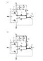
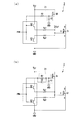
図4は、本発明の第1実施形態の変形例に係る半導体素子の駆動回路の構成を示す回路図である。図4(a)に示す通り、駆動回路1に設けられるダイオードD1(遅延回路13の抵抗R1に並列に接続されているダイオード)は、半導体素子Q1のターンオフ特性の悪化が引き起こされなければ省略することが可能である。また、図4(b)に示す通り、ゲート抵抗Rg3を省略することも可能である。ゲート抵抗Rg3を省略することで、スイッチング用MOSFETQ4がオン状態になった場合の半導体素子Q1のゲート抵抗の抵抗値をより小さくすることができ、半導体素子Q1のターンオン動作が加速度をより高めることができる。
FIG. 4 is a circuit diagram showing a configuration of a semiconductor element drive circuit according to a modification of the first embodiment of the present invention. As shown in FIG. 4A, the diode D1 (diode connected in parallel to the resistor R1 of the delay circuit 13) provided in the
〔第2実施形態〕
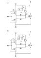
図5は、本発明の第2実施形態による半導体素子の駆動回路の構成を示す回路図である。図5に示す通り、本実施形態の駆動回路2は、図1に示す駆動回路1の反転回路12を省略し、ゲート抵抗Rg3、スイッチング用MOSFETQ4、遅延回路13、及びダイオードD1を、それぞれゲート抵抗Rg4(第2抵抗部)、スイッチング用MOSFETQ5(第2スイッチ素子)、遅延回路23、及びダイオードD3に代えた構成である。
[Second Embodiment]
FIG. 5 is a circuit diagram showing a configuration of a drive circuit for a semiconductor device according to the second embodiment of the present invention. As shown in FIG. 5, the
ゲート抵抗Rg4は、一端が半導体素子Q1のゲートGに接続されており、他端がスイッチング用MOSFETQ5のソースに接続されている。ゲート抵抗Rg4の抵抗値は、第1実施形態と同様に、ゲート抵抗Rg1との合成抵抗(ゲート抵抗Rg1,Rg4が並列接続された状態の合成抵抗)が、ゲート抵抗Rg1の抵抗値よりも十分に小さくなるように設定される。 One end of the gate resistor Rg4 is connected to the gate G of the semiconductor element Q1, and the other end is connected to the source of the switching MOSFET Q5. As in the first embodiment, the resistance value of the gate resistance Rg4 is sufficiently higher than the resistance value of the gate resistance Rg1 when the combined resistance with the gate resistance Rg1 (the combined resistance when the gate resistances Rg1 and Rg4 are connected in parallel) is sufficient. Is set to be smaller.
スイッチング用MOSFETQ5は、nチャネルMOSFETであり、ゲートが遅延回路23の出力端に接続されており、ドレインが電源Vccに接続されており、ソースがゲート抵抗Rg4の他端に接続されている。従って、スイッチング用MOSFETQ5の導通時には、ゲート抵抗Rg4を流れる電源Vccからのゲート電流によって、半導体素子Q1のゲートGが充電される。スイッチング用MOSFETQ4の導通時におけるゲート電流は、ゲート抵抗Rg4の抵抗値に応じた大きさである。
The switching MOSFET Q5 is an n-channel MOSFET, the gate is connected to the output terminal of the
遅延回路23は、抵抗R2及びコンデンサC2を備えており、PWM信号を予め規定された時間だけ遅延させる。抵抗R2は、一端がスイッチング用MOSFETQ5のゲートに接続され、他端がトランジスタQ2,Q3のベースに接続されている。つまり、抵抗R2の他端には、PWM信号が入力される。コンデンサC2は、一端がスイッチング用MOSFETQ5のゲートに接続され、他端が接地されている。
The
尚、遅延回路23の遅延時間は、コンデンサC2及び抵抗R2で定まる遅延回路23の時定数に応じた時間である。ここでは、第1実施形態と同様の遅延時間(t2−t1)であるとする。ダイオードD2は、図1に示すダイオードD1と同様に、半導体素子Q1のターンオフ動作中に、コンデンサC2に充電された電荷を素早く放電するためのものである。
The delay time of the
次に、上記構成における駆動回路2の動作について説明する。図6は、本発明の第2実施形態による半導体素子の駆動回路の動作を説明するためのタイミングチャートである。また、図7は、本発明の第2実施形態におけるゲート電流の経路を示す図である。尚、本実施形態においても、第1実施形態と同様に、時刻t1においてPWM信号がHighレベルになって半導体素子Q1のターンオン指令が駆動回路1に入力されるものとする。
Next, the operation of the
半導体素子Q1のターンオン指令が入力されると、増幅部11に設けられたトランジスタQ2がオン状態になり、図7(a)に示す電流経路CP1を介してゲート電流が流れ、このゲート電流によって半導体素子Q1のゲートGが充電される。これにより、図6に示す通り、半導体素子Q1のゲート電圧Vgsが上昇する。ゲート電圧Vgsが徐々に上昇していくと、第1実施形態と同様に、半導体素子Q1にドレイン電流Idが流れ始める(図6中の時刻t11)。そして、図6に示す通り、ドレイン電流Idは、時刻t12になるまで時間の経過とともに上昇する。尚、半導体素子Q1のドレイン電圧Vdsは、時刻t12までは一定の値である。
When a turn-on command for the semiconductor element Q1 is input, the transistor Q2 provided in the amplifying
また、半導体素子Q1のターンオン指令が入力されると(時刻t1)、遅延回路23のコンデンサC2の充電が開始され、スイッチング用MOSFETQ5のゲート電圧が上昇する。PWM信号がHighレベルになった時点から上記の遅延時間(t2−t1)が経過すると(時刻t2になると)、図6に示す通り、スイッチング用MOSFETQ5のゲート電圧が閾値を超えてオン状態になり、ゲート抵抗Rg4がゲート抵抗Rg1と並列接続された状態になる。これにより、半導体素子Q1のゲート抵抗の抵抗値は、ゲート抵抗Rg1の抵抗値から、ゲート抵抗Rg1とゲート抵抗Rg4とが並列接続された抵抗値(ゲート抵抗Rg1の抵抗値よりも小さな抵抗値)に切り替わる。
When a turn-on command for the semiconductor element Q1 is input (time t1), charging of the capacitor C2 of the
すると、図7(b)に示す通り、電流経路CP1に加えて電流経路CP3を介してゲート電流が流れ、これら電流経路CP1,CP3を介するゲート電流によって半導体素子Q1のゲートGが充電される。尚、図7(b)に示す電流経路CP3は、電源Vccからスイッチング用MOSFETQ5及びゲート抵抗Rg4を順に介して半導体素子Q1のゲートGに至る経路である。 Then, as shown in FIG. 7B, a gate current flows through the current path CP3 in addition to the current path CP1, and the gate G of the semiconductor element Q1 is charged by the gate currents through the current paths CP1 and CP3. A current path CP3 shown in FIG. 7B is a path from the power supply Vcc to the gate G of the semiconductor element Q1 through the switching MOSFET Q5 and the gate resistor Rg4 in this order.
これにより、図6に示す通り、半導体素子Q1のゲート電圧Vgsの時間変化率が、ゲート抵抗の抵抗値が切り替わらない場合(点線で示す場合)に比べて高くなり、半導体素子Q1のターンオン動作が加速される。しかしながら、本実施形態では、スイッチング用MOSFETQ5としてnチャネルMOSFETを用いているため、半導体素子Q1のゲート電圧Vgsが電源Vccの電圧になると、スイッチング用MOSFETQ5がオフ状態になってしまう(時刻t3)。これにより、半導体素子Q1のゲート抵抗の抵抗値が、ゲート抵抗Rg1とゲート抵抗Rg4とが並列接続された抵抗値から、ゲート抵抗Rg1の抵抗値に切り替わり、半導体素子Q1のターンオン動作の加速が停止されてしまう。 As a result, as shown in FIG. 6, the time change rate of the gate voltage Vgs of the semiconductor element Q1 is higher than when the resistance value of the gate resistance is not switched (indicated by the dotted line), and the turn-on operation of the semiconductor element Q1 is performed. Accelerated. However, in this embodiment, since an n-channel MOSFET is used as the switching MOSFET Q5, the switching MOSFET Q5 is turned off when the gate voltage Vgs of the semiconductor element Q1 becomes the voltage of the power supply Vcc (time t3). Thereby, the resistance value of the gate resistance of the semiconductor element Q1 is switched from the resistance value in which the gate resistance Rg1 and the gate resistance Rg4 are connected in parallel to the resistance value of the gate resistance Rg1, and the acceleration of the turn-on operation of the semiconductor element Q1 is stopped. Will be.
但し、半導体素子Q1のターンオン動作の加速が停止されたとしても、時刻t2〜t3の間は間違いなく半導体素子Q1のターンオン動作が加速されている。このため、ゲート電圧Vgsがピーク値に達するタイミング(ドレイン電圧Vdsがゼロに達するタイミング)は、ゲート抵抗の抵抗値が切り替わらない場合の時刻t22よりも早い時刻t31になる。 However, even if the acceleration of the turn-on operation of the semiconductor element Q1 is stopped, the turn-on operation of the semiconductor element Q1 is definitely accelerated between the times t2 and t3. For this reason, the timing at which the gate voltage Vgs reaches the peak value (the timing at which the drain voltage Vds reaches zero) is the time t31 earlier than the time t22 when the resistance value of the gate resistance is not switched.
以上の通り、本実施形態においても、半導体素子Q1のターンオン動作中における急峻なドレイン電流Idの変化が、遅延回路23による遅延時間(t2−t1)内において生ずるように遅延回路23の時定数を設定している。そして、半導体素子Q1のターンオン指令が入力される時刻t1から遅延回路23の遅延が終了する時刻t2までは、ゲート抵抗Rg1を介するゲート電流によって半導体素子Q1のゲートGを充電し、時刻t2〜t3の間は、ゲート抵抗Rg1,Rg2を介するゲート電流によって半導体素子Q1のゲートGを充電するようにしている。
As described above, also in the present embodiment, the time constant of the
これにより、半導体素子Q1のターンオン動作時における急峻なドレイン電流Idの変化が生ずる期間が含まれる時刻t1〜t2の間は、半導体素子Q1のターンオン動作を遅くすることができるため、サージ電圧やノイズを抑制することができる。また、時刻t2〜t3の間は、半導体素子Q1のターンオン動作を速くすることができるため、半導体素子Q1のスイッチング損失を低く抑えることができる。 As a result, the turn-on operation of the semiconductor element Q1 can be delayed between the times t1 and t2 including the period in which the steep drain current Id changes during the turn-on operation of the semiconductor element Q1. Can be suppressed. Further, since the turn-on operation of the semiconductor element Q1 can be accelerated between the times t2 and t3, the switching loss of the semiconductor element Q1 can be suppressed to a low level.
また、本実施形態では、図1に示す反転回路12を省略することができるため、第1実施形態よりも簡易な回路構成を実現することができる。尚、本実施形態と第1実施形態とは、PWM信号の論理反転を行っているか否かの違いがあるものの、基本的にはPWM信号を遅延させた信号によってスイッチング用MOSFETQ4,Q5を制御している点は共通する。このため、本実施形態においても、安定して半導体素子Q1を駆動することができ、半導体素子Q1が設けられる各種装置(モータ駆動装置、発電装置、電動コンプレッサ、電力変換装置等)の安定動作に資することができる。
Further, in this embodiment, since the inverting
図8は、本発明の第2実施形態の変形例に係る半導体素子の駆動回路の構成を示す回路図である。図8(a)に示す通り、駆動回路2に設けられるダイオードD2(遅延回路23の抵抗R2に並列に接続されているダイオード)は、第1実施形態のダイオードD1と同様に省略することが可能である。また、図8(b)に示す通り、第1実施形態のゲート抵抗Rg3と同様に、ゲート抵抗Rg4を省略することも可能である。
FIG. 8 is a circuit diagram showing a configuration of a semiconductor element drive circuit according to a modification of the second embodiment of the present invention. As shown in FIG. 8A, the diode D2 (diode connected in parallel to the resistor R2 of the delay circuit 23) provided in the
以上、本発明の実施形態による半導体素子の駆動回路について説明したが、本発明は上記実施形態に制限されず、本発明の範囲内で自由に変更が可能である。例えば、上記実施形態では、駆動対象である半導体素子Q1が、例えばシリコンよりもバンドギャップが大きい半導体材料を基板に含むワイドバンドギャップのパワーMOSFETである場合を例に挙げて説明したが、半導体素子Q1は、ワイドバンドギャップのIGBTであっても良い。尚、半導体素子Q1は、シリコンを基板材料とするMOSFETやIGBT等であっても良い。 Although the semiconductor element driving circuit according to the embodiment of the present invention has been described above, the present invention is not limited to the above-described embodiment, and can be freely changed within the scope of the present invention. For example, in the above-described embodiment, the semiconductor element Q1 to be driven is described as an example of the case where the semiconductor element Q1 is a wide band gap power MOSFET including a semiconductor material having a larger band gap than silicon, for example. Q1 may be a wide band gap IGBT. The semiconductor element Q1 may be a MOSFET, IGBT or the like using silicon as a substrate material.
また、上述した第1,第2実施形態における増幅部11に設けられたトランジスタQ2はnチャネルMOSFETでも良く、トランジスタQ3はpチャネルMOSFETでも良い。また、第1実施形態におけるスイッチング用MOSFETQ4は、PNPトランジスタであっても良く、第2実施形態におけるスイッチング用MOSFETQ5は、NPNトランジスタであっても良い。
Further, the transistor Q2 provided in the amplifying
1,2…駆動回路、12…反転回路、13,23…遅延回路、C1,C2…コンデンサ、G…ゲート、Q1…半導体素子、Q2…NPNトランジスタ、Q4,Q5…スイッチング用MOSFET、R1,R2…抵抗、Rg1〜Rg4…ゲート抵抗、Vcc…電源
DESCRIPTION OF
Claims (6)
前記指令信号を予め規定された時間だけ遅延させる遅延回路と、
前記遅延回路で遅延された前記指令信号に基づいて、前記電源と前記制御電極とを接続する第2スイッチ素子と、
を備える半導体素子の駆動回路。 A first resistor having one end connected to the control electrode of the semiconductor element and a first resistor that is turned on based on a command signal that commands the on-state of the semiconductor element and connects the power source and the other end of the first resistor. In a drive circuit for a semiconductor element comprising one switch element,
A delay circuit for delaying the command signal by a predetermined time;
A second switch element for connecting the power source and the control electrode based on the command signal delayed by the delay circuit;
A drive circuit for a semiconductor device comprising:
前記指令信号の論理を反転させて前記遅延回路に出力する反転回路を備える、
請求項1記載の半導体素子の駆動回路。 The second switch element is a p-channel MOSFET in which the command signal delayed by the delay circuit is input to a gate,
An inverting circuit that inverts the logic of the command signal and outputs the inverted signal to the delay circuit;
A drive circuit for a semiconductor device according to claim 1.
前記pチャネルMOSFETのゲートとソースとの間に接続されたコンデンサと、
を備える請求項2記載の半導体素子の駆動回路。 The delay circuit includes a resistor connected in series between the inverting circuit and the gate of the p-channel MOSFET;
A capacitor connected between the gate and source of the p-channel MOSFET;
The drive circuit of the semiconductor element of Claim 2 provided with.
一端が前記nチャネルMOSFETのゲートに接続され、他端が接地されたコンデンサと、
を備える請求項4記載の半導体素子の駆動回路。 The delay circuit has one end connected to the gate of the n-channel MOSFET and the other end connected to the command signal.
A capacitor having one end connected to the gate of the n-channel MOSFET and the other end grounded;
A drive circuit for a semiconductor device according to claim 4.
Priority Applications (1)
| Application Number | Priority Date | Filing Date | Title |
|---|---|---|---|
| JP2016001772A JP2017123732A (en) | 2016-01-07 | 2016-01-07 | Driving circuit of semiconductor device |
Applications Claiming Priority (1)
| Application Number | Priority Date | Filing Date | Title |
|---|---|---|---|
| JP2016001772A JP2017123732A (en) | 2016-01-07 | 2016-01-07 | Driving circuit of semiconductor device |
Publications (1)
| Publication Number | Publication Date |
|---|---|
| JP2017123732A true JP2017123732A (en) | 2017-07-13 |
Family
ID=59305869
Family Applications (1)
| Application Number | Title | Priority Date | Filing Date |
|---|---|---|---|
| JP2016001772A Pending JP2017123732A (en) | 2016-01-07 | 2016-01-07 | Driving circuit of semiconductor device |
Country Status (1)
| Country | Link |
|---|---|
| JP (1) | JP2017123732A (en) |
Cited By (1)
| Publication number | Priority date | Publication date | Assignee | Title |
|---|---|---|---|---|
| CN112714988A (en) * | 2018-09-19 | 2021-04-27 | 松下知识产权经营株式会社 | Surge current suppression device and motor drive device |
Citations (3)
| Publication number | Priority date | Publication date | Assignee | Title |
|---|---|---|---|---|
| JP2004088892A (en) * | 2002-08-26 | 2004-03-18 | Toshiba Corp | Gate circuit of insulated gate semiconductor device |
| JP2006340579A (en) * | 2005-06-06 | 2006-12-14 | Toshiba Mitsubishi-Electric Industrial System Corp | Gate circuit of insulating gate semiconductor element |
| JP2015177694A (en) * | 2014-03-17 | 2015-10-05 | 株式会社Ihi | Drive circuit for voltage driven power semiconductor device |
-
2016
- 2016-01-07 JP JP2016001772A patent/JP2017123732A/en active Pending
Patent Citations (3)
| Publication number | Priority date | Publication date | Assignee | Title |
|---|---|---|---|---|
| JP2004088892A (en) * | 2002-08-26 | 2004-03-18 | Toshiba Corp | Gate circuit of insulated gate semiconductor device |
| JP2006340579A (en) * | 2005-06-06 | 2006-12-14 | Toshiba Mitsubishi-Electric Industrial System Corp | Gate circuit of insulating gate semiconductor element |
| JP2015177694A (en) * | 2014-03-17 | 2015-10-05 | 株式会社Ihi | Drive circuit for voltage driven power semiconductor device |
Cited By (2)
| Publication number | Priority date | Publication date | Assignee | Title |
|---|---|---|---|---|
| CN112714988A (en) * | 2018-09-19 | 2021-04-27 | 松下知识产权经营株式会社 | Surge current suppression device and motor drive device |
| CN112714988B (en) * | 2018-09-19 | 2023-07-25 | 松下知识产权经营株式会社 | Inrush Current Suppressors and Motor Drives |
Similar Documents
| Publication | Publication Date | Title |
|---|---|---|
| US9083343B1 (en) | Cascode switching circuit | |
| JP5629386B2 (en) | Semiconductor drive circuit and power converter using the same | |
| CN107615664B (en) | Power transistor driving device | |
| US8773177B2 (en) | Drive circuit | |
| JP4512671B1 (en) | Power conversion circuit | |
| JP5993749B2 (en) | Gate drive circuit of semiconductor device and power conversion device using the same | |
| CN102208864A (en) | Switching device driving unit and semiconductor apparatus | |
| CN105471417B (en) | The control circuit of IGBT for reverse-conducting | |
| JP6303663B2 (en) | Voltage-driven power semiconductor element drive circuit | |
| JP6458552B2 (en) | Switching type step-down DC-DC converter and power conversion circuit | |
| CN105099417A (en) | Arrangement and method for a power semiconductor switch | |
| JP2013081137A (en) | Semiconductor device | |
| KR102026929B1 (en) | Gate driving circuit for power switch | |
| JP2018098849A (en) | Power module | |
| JP6456524B2 (en) | Buffer circuit and semiconductor device | |
| JP2017123732A (en) | Driving circuit of semiconductor device | |
| JP2009017723A (en) | Drive circuit of current amplification semiconductor element | |
| CN116683752A (en) | Drive control circuit and control method | |
| Bayerer et al. | Low impedance gate drive for full control of voltage controlled power devices | |
| JP5780489B2 (en) | Gate drive circuit | |
| CN114362729A (en) | Gate drive circuit adaptive to high junction temperature environment and switching-on method and switching-off method thereof | |
| WO2016192799A1 (en) | Parallel-coupled switching devices and switch-mode power converter | |
| JP5791758B1 (en) | Gate drive circuit | |
| JP6312946B1 (en) | Power semiconductor element drive circuit and motor drive device | |
| JP5950961B2 (en) | Gate drive circuit |
Legal Events
| Date | Code | Title | Description |
|---|---|---|---|
| A521 | Request for written amendment filed |
Free format text: JAPANESE INTERMEDIATE CODE: A821 Effective date: 20160108 |
|
| RD03 | Notification of appointment of power of attorney |
Free format text: JAPANESE INTERMEDIATE CODE: A7423 Effective date: 20181109 |
|
| A621 | Written request for application examination |
Free format text: JAPANESE INTERMEDIATE CODE: A621 Effective date: 20181127 |
|
| A131 | Notification of reasons for refusal |
Free format text: JAPANESE INTERMEDIATE CODE: A131 Effective date: 20190924 |
|
| A977 | Report on retrieval |
Free format text: JAPANESE INTERMEDIATE CODE: A971007 Effective date: 20190925 |
|
| A521 | Request for written amendment filed |
Free format text: JAPANESE INTERMEDIATE CODE: A523 Effective date: 20191009 |
|
| A02 | Decision of refusal |
Free format text: JAPANESE INTERMEDIATE CODE: A02 Effective date: 20200107 |
|
| A521 | Request for written amendment filed |
Free format text: JAPANESE INTERMEDIATE CODE: A523 Effective date: 20200406 |
|
| C60 | Trial request (containing other claim documents, opposition documents) |
Free format text: JAPANESE INTERMEDIATE CODE: C60 Effective date: 20200406 |
|
| A911 | Transfer to examiner for re-examination before appeal (zenchi) |
Free format text: JAPANESE INTERMEDIATE CODE: A911 Effective date: 20200414 |
|
| C21 | Notice of transfer of a case for reconsideration by examiners before appeal proceedings |
Free format text: JAPANESE INTERMEDIATE CODE: C21 Effective date: 20200421 |
|
| A912 | Re-examination (zenchi) completed and case transferred to appeal board |
Free format text: JAPANESE INTERMEDIATE CODE: A912 Effective date: 20200619 |
|
| C211 | Notice of termination of reconsideration by examiners before appeal proceedings |
Free format text: JAPANESE INTERMEDIATE CODE: C211 Effective date: 20200623 |
|
| C22 | Notice of designation (change) of administrative judge |
Free format text: JAPANESE INTERMEDIATE CODE: C22 Effective date: 20201006 |
|
| C23 | Notice of termination of proceedings |
Free format text: JAPANESE INTERMEDIATE CODE: C23 Effective date: 20201124 |
|
| C03 | Trial/appeal decision taken |
Free format text: JAPANESE INTERMEDIATE CODE: C03 Effective date: 20210105 |
|
| C30A | Notification sent |
Free format text: JAPANESE INTERMEDIATE CODE: C3012 Effective date: 20210105 |