JP2017117845A - Semiconductor light emitting element and manufacturing method of the same - Google Patents
Semiconductor light emitting element and manufacturing method of the same Download PDFInfo
- Publication number
- JP2017117845A JP2017117845A JP2015248898A JP2015248898A JP2017117845A JP 2017117845 A JP2017117845 A JP 2017117845A JP 2015248898 A JP2015248898 A JP 2015248898A JP 2015248898 A JP2015248898 A JP 2015248898A JP 2017117845 A JP2017117845 A JP 2017117845A
- Authority
- JP
- Japan
- Prior art keywords
- layer
- barrier layer
- light emitting
- semiconductor light
- growth
- Prior art date
- Legal status (The legal status is an assumption and is not a legal conclusion. Google has not performed a legal analysis and makes no representation as to the accuracy of the status listed.)
- Granted
Links
Images


Abstract
Description
本発明は、半導体発光素子およびその製造方法に関し、特に多重量子井戸構造と電子ブロック層を備える半導体発光素子およびその製造方法に関する。 The present invention relates to a semiconductor light emitting device and a method for manufacturing the same, and more particularly to a semiconductor light emitting device including a multiple quantum well structure and an electron block layer and a method for manufacturing the same.
従来から、発光ダイオードなどの半導体発光素子の発光効率を高めるために、活性層として障壁層と井戸層を交互に積層した多重量子井戸(MQW:Multi Quantum Well)構造が採用されている。また、MQW活性層を構成する最上層の障壁層であるラストバリア層上に、障壁層よりも電子障壁が高い材料で電子ブロック層を形成し、p型半導体層側にキャリアがオーバーフローすることを防止して、MQW活性層へのキャリアの閉じ込めを高めるものも提案されている(例えば特許文献1,2等)。
Conventionally, in order to increase the light emission efficiency of a semiconductor light emitting device such as a light emitting diode, a multiple quantum well (MQW) structure in which barrier layers and well layers are alternately stacked as an active layer has been adopted. Further, an electron block layer is formed of a material having an electron barrier higher than that of the barrier layer on the last barrier layer which is the uppermost barrier layer constituting the MQW active layer, and carriers overflow to the p-type semiconductor layer side. Some have been proposed to prevent the trapping of carriers in the MQW active layer (for example,
図6は従来技術における半導体発光素子のラストバリア層と電子ブロック層の成長方法を示すタイミングチャートである。窒化物系材料を用いた半導体発光素子では、ラストバリア層であるGaN層を成長させた後に、電子ブロック層としてAlGaN層を成長させ、その後にp型GaN層を成長させている。 FIG. 6 is a timing chart showing a growth method of the last barrier layer and the electron block layer of the semiconductor light emitting device in the prior art. In a semiconductor light emitting device using a nitride material, after a GaN layer as a last barrier layer is grown, an AlGaN layer is grown as an electron blocking layer, and then a p-type GaN layer is grown.
図6に示すように、ラストバリア層の成長工程では成長温度を800℃に維持して、窒素原料となるアンモニアとガリウム原料となるTEG(Triethylgallium)を流してGaN層を成長させる。次に、アンモニアの流量は維持してTEGの供給を停止し、温度を800℃から900℃まで昇温する。この昇温工程では、ガリウム原料であるTEGの供給が停止しているのでGaN層の成長は中断している。 As shown in FIG. 6, in the growth process of the last barrier layer, the growth temperature is maintained at 800 ° C., and ammonia as a nitrogen material and TEG (Triethylgallium) as a gallium material are flown to grow a GaN layer. Next, the supply of TEG is stopped while maintaining the flow rate of ammonia, and the temperature is raised from 800 ° C. to 900 ° C. In this temperature raising step, the growth of the GaN layer is interrupted because the supply of TEG, which is a gallium raw material, is stopped.
次に、成長温度900℃でアンモニアとTMG(Trimethylgallium)とTMA(Trimethylaluminium)とCp2Mg(Bis(cyclopentadienyl)magnesium)を供給しp型不純物としてMgを含んだAlGaN電子ブロック層を成長する。次に成長温度を900℃に維持したままTMAの供給を停止してp型GaN層を成長する。 Next, an AlGaN electron block layer containing Mg as a p-type impurity is grown by supplying ammonia, TMG (Trimethylgallium), TMA (Trimethylaluminum), and Cp 2 Mg (Bis (cyclopentadienyl) magnesium) at a growth temperature of 900 ° C. Next, the supply of TMA is stopped while maintaining the growth temperature at 900 ° C., and a p-type GaN layer is grown.
引用文献1,2の従来技術では、MQW活性層を成長させる温度よりも高い温度で電子ブロック層を成長させるため、ラストバリア層を成長させた後にキャリアガスとアンモニアガスのみを流して成長を中断し、成長中断の間に電子ブロック層の成長温度まで昇温し、昇温後に原料ガスを流して電子ブロック層を成長させていた。
In the prior arts of the cited
しかし、昇温中に成長中断している間にも、ラストバリア層の表面は高温状態で成長装置内に曝されることになり、表面状態が悪化して結晶品質が低下してしまい、結果として半導体発光素子の発光効率が低下するという問題があった。 However, even while the growth is interrupted during the temperature rise, the surface of the last barrier layer will be exposed to the inside of the growth apparatus at a high temperature state, the surface state will deteriorate and the crystal quality will deteriorate. As a problem, the luminous efficiency of the semiconductor light emitting device is reduced.
そこで本発明は、上記従来の問題点に鑑みなされたものであり、ラストバリア層の表面状態を良好にして結晶品質を維持し、発光効率を向上させることが可能な半導体発光素子およびその製造方法を提供することを目的とする。 Accordingly, the present invention has been made in view of the above-described conventional problems, and a semiconductor light emitting device capable of maintaining the crystal quality by improving the surface state of the last barrier layer and improving the light emission efficiency, and a method for manufacturing the same. The purpose is to provide.
上記課題を解決するために、本発明の半導体発光素子は、障壁層と井戸層を交互に積層した多重量子井戸活性層と、前記多重量子井戸活性層の上に形成された電子ブロック層とを備える半導体発光素子であって、前記障壁層のうち最上層であるラストバリア層は、他の前記障壁層よりも厚く、前記電子ブロック層からの不純物が拡散されている拡散領域と、前記電子ブロック層からの不純物が到達していない非拡散領域とを備えていることを特徴とする。 In order to solve the above problems, a semiconductor light emitting device of the present invention comprises a multiple quantum well active layer in which barrier layers and well layers are alternately stacked, and an electron block layer formed on the multiple quantum well active layer. A last barrier layer, which is the uppermost layer of the barrier layers, is thicker than the other barrier layers, a diffusion region in which impurities from the electron block layer are diffused, and the electron block And a non-diffusion region to which impurities from the layer do not reach.
このような本発明の半導体発光素子では、ラストバリア層が障壁層よりも厚く形成されてラストバリア層の表面状態が良好であり、電子ブロック層から拡散した不純物がラストバリア層の内部で止まるため、多重量子井戸活性層への不純物拡散の影響を防止して発光効率を向上させることができる。 In such a semiconductor light emitting device of the present invention, the last barrier layer is formed thicker than the barrier layer, the surface state of the last barrier layer is good, and impurities diffused from the electron block layer stop inside the last barrier layer. Therefore, it is possible to improve the luminous efficiency by preventing the influence of impurity diffusion to the multiple quantum well active layer.
また、前記ラストバリア層の膜厚は、前記他の障壁層の膜厚の1.5〜3倍としてもよい。 The film thickness of the last barrier layer may be 1.5 to 3 times the film thickness of the other barrier layer.
また、前記ラストバリア層の膜厚は、20nm以上30nm以下の範囲としてもよい。 The film thickness of the last barrier layer may be in the range of 20 nm to 30 nm.
上記課題を解決するために、本発明の半導体発光素子の製造方法は、障壁層と井戸層を交互に積層した多重量子井戸活性層を成長させ、前記多重量子井戸活性層の上に電子ブロック層を成長させる半導体発光素子の製造方法であって、前記障壁層のうち最上層であるラストバリア層を成長させる工程は、他の前記障壁層と同じ温度条件で結晶成長させる定温成長工程と、前記定温成長工程の後に成長温度を上昇させながら結晶成長を継続する昇温成長工程とを備えることを特徴とする。 In order to solve the above-described problems, a method of manufacturing a semiconductor light emitting device according to the present invention includes growing a multiple quantum well active layer in which barrier layers and well layers are alternately stacked, and forming an electron block layer on the multiple quantum well active layer. A step of growing a last barrier layer, which is the uppermost layer of the barrier layers, includes a constant temperature growth step of crystal growth under the same temperature conditions as the other barrier layers, And a temperature rising growth step of continuing crystal growth while raising the growth temperature after the constant temperature growth step.
このような本発明の半導体発光素子の製造方法では、ラストバリア層の成長工程として定温成長工程の後に昇温成長工程を備えることで、ラストバリア層の表面状態が良好になり、発光効率を向上させることができる。 In such a method of manufacturing a semiconductor light emitting device of the present invention, the surface condition of the last barrier layer is improved and the luminous efficiency is improved by providing the temperature rising growth step after the constant temperature growth step as the last barrier layer growth step. Can be made.
また、前記ラストバリア層の膜厚は、前記他の障壁層の膜厚よりも厚くしてもよい。 The film thickness of the last barrier layer may be larger than the film thickness of the other barrier layer.
また、前記定温成長工程で成長させる前記ラストバリア層の膜厚は、前記他の障壁層の膜厚以上でもよい。 The film thickness of the last barrier layer grown in the constant temperature growth step may be equal to or greater than the film thickness of the other barrier layer.
また、前記電子ブロック層の成長時および成長後に、前記電子ブロック層から前記ラストバリア層に不純物の拡散が生じ、前記ラストバリア層に前記電子ブロック層からの不純物が拡散されている拡散領域と、前記電子ブロック層からの不純物が到達していない非拡散領域とが形成されるとしてもよい。 Further, during and after the growth of the electron blocking layer, diffusion of impurities occurs from the electron blocking layer to the last barrier layer, and a diffusion region in which impurities from the electron blocking layer are diffused to the last barrier layer; A non-diffusion region to which impurities from the electron blocking layer have not reached may be formed.
本発明では、ラストバリア層の表面状態を良好にして結晶品質を維持し、発光効率を向上させることが可能な半導体発光素子およびその製造方法を提供することができる。 In the present invention, it is possible to provide a semiconductor light emitting device capable of improving the light emission efficiency by improving the surface state of the last barrier layer, maintaining the crystal quality, and the manufacturing method thereof.
(第1実施形態)
以下、本発明の実施の形態について、図面を参照して詳細に説明する。各図面に示される同一または同等の構成要素、部材、処理には、同一の符号を付すものとし、適宜重複した説明は省略する。
(First embodiment)
Hereinafter, embodiments of the present invention will be described in detail with reference to the drawings. The same or equivalent components, members, and processes shown in the drawings are denoted by the same reference numerals, and repeated descriptions are omitted as appropriate.
図1は、本実施形態における半導体発光素子1の層構造を示す模式図である。半導体発光素子1は、サファイア基板10上に、GaNバッファ層11と、GaN下地層12と、n型GaN下地層13と、発光層14と、電子ブロック層15と、p型GaNコンタクト層16とを備えている。
FIG. 1 is a schematic view showing a layer structure of a semiconductor
サファイア基板10は、サファイア単結晶のc面を主面として切り出した基板である。ここではc面を主面とするサファイア基板10を示したが、c面から所定の結晶軸方向に傾斜させたオフ基板としてもよく、c面以外のa面やm面、r面やその他の高次数な面方位を主面としてもよい。
The
GaNバッファ層11は、サファイア基板10の主面に形成したGaNからなる緩衝層であり、例えば500℃程度の比較的低温で成長される。GaN下地層12は、意図的に不純物を含まないノンドープとして成長されたGaNの単結晶からなる層である。GaN下地層12の膜厚としては例えば3000nm程度であるが、必要に応じて適宜調整してもよい。n型GaN下地層13は、n型不純物としてSiをドープされたGaNの単結晶からなる層である。n型GaN下地層13の膜厚としては例えば3000nm程度であり、不純物濃度としては例えば1×1019cm-3程度であるが、必要に応じて適宜調整してもよい。
The GaN
発光層14は、井戸層と障壁層(バリア層)を交互に積層した多重量子井戸活性層である。電子ブロック層15は、発光層14上に形成されてキャリアのオーバーフローを防止するための半導体層であり、障壁層よりも電子に対する障壁が大きな材料で構成されている。p型GaNコンタクト層16は、p型不純物としてMgをドープされたGaNの単結晶からなる層である。
The
p型GaNコンタクト層16の不純物濃度としては例えば1×1019cm-3程度であるが、1×1018cm-3〜5×1020cm-3程度の範囲であればよい。p型GaNコンタクト層16の好ましい膜厚の範囲としては50〜150nmであり、より好ましくは80〜100nmである。
The impurity concentration of the p-type
図1では半導体発光素子1に電極を示していないが、半導体発光素子として公知の電極構造を採用しても良く、例えばn型GaN下地層13が露出するまで半導体層の一部領域をエッチングしてn側電極を形成し、p型GaNコンタクト層16上にp側電極を形成する。発光層14、電子ブロック層15、p型GaNコンタクト層16の構造についての詳細は後述する。
Although no electrode is shown in the semiconductor
ここでバッファ層、GaN下地層、p型コンタクト層を構成する材料として、GaNバッファ層11、GaN下地層12、n型GaN下地層13、p型GaNコンタクト層16のようにGaN層を例として挙げたが、AlGaNやInGaN、InAlGaNなどの他の材料を用いてもよい。また、必要に応じてクラッド層や電流狭窄層、電流拡散層など、半導体発光素子に用いられる従来公知の構造を適用してもよい。また、n型の下地層としてGaNの例を示したが、n型のAlGaNからなる層を下地層としてもよい。
Here, as a material constituting the buffer layer, the GaN underlayer, and the p-type contact layer, GaN layers such as the
図2は、図1に示した発光層14の構造を詳細に説明する模式図である。図2に示すように本実施形態の発光層14は、バリア層14aと井戸層14bを交互に5周期繰り返して形成し、最後の井戸層14b上にラストバリア層14cが形成された構造である。バリア層14aとしては例えば膜厚が12nmのGaN層が挙げられ、井戸層14bとしては例えば膜厚が3nmのInGaN層が挙げられる。
FIG. 2 is a schematic diagram for explaining in detail the structure of the
バリア層14aの好ましい膜厚の範囲としては5〜15nmであり、より好ましくは8〜12nmである。井戸層14bの好ましい膜厚の範囲としては2〜4nmであり、より好ましくは2.5〜3.5nmである。ラストバリア層14cは、バリア層14aと同じ材料であるGaNにより構成され、その膜厚はバリア層14aよりも厚く形成され、好ましい膜厚の範囲はバリア層14aの1.5〜3倍程度の膜厚の15〜30nmであり、より好ましくは20〜30nmである。
The preferable film thickness range of the
電子ブロック層15は、ラストバリア層14cの上に形成されており、ラストバリア層14cよりも電子に対する障壁が大きい材料で構成されて、多重量子井戸構造の発光層14からp型GaNコンタクト層16へのキャリアのオーバーフローを防止する。電子ブロック層15としては、例えばp型不純物としてMgが1×1018cm-3〜5×1020cm-3程度ドープされたp型AlGaN層であり、好ましい膜厚の範囲は10〜40nmであり、より好ましくは20〜30nmである。
The
ここではバリア層14a及びラストバリア層14cを構成する材料としてGaNを挙げ、井戸層14bを構成する材料としてInGaNを挙げ、電子ブロック層15を構成する材料としてAlGaNを挙げたが、他の材料であってもよい。また、図2では発光層14として5周期の多重量子井戸構造を示したが、周期数は適宜調整してもよい。
Here, GaN is given as a material constituting the
次に、本実施形態の半導体発光素子1の製造方法を説明する。半導体発光素子1は、従来から用いられている有機金属気相成長法(MOCVD: Metal Organic Chemical Vapor Deposition)により各層を成長することで製造される。本実施形態の半導体発光素子1の製造方法の一部として、ラストバリア層14cからp型GaNコンタクト層16までの成長工程を示すタイミングチャートを図3に示す。
Next, a method for manufacturing the semiconductor
はじめに、MOCVD装置の反応炉にサファイア基板10を設置し、基板温度を500℃まで上昇させ、キャリアガスとして水素を流しながら、原料ガスとしてTMGおよびアンモニアを供給する。これにより、サファイア基板10の主面上に低温バッファ層であるGaNバッファ層11を数百nmの膜厚で形成する。
First, the
次に、基板温度を1000℃まで上昇させて、キャリアガスとして水素を流しながら、原料ガスとしてTMGおよびアンモニアを供給する。これによりGaNバッファ層11上にGaN下地層12を3000nmの膜厚で形成する。
Next, the substrate temperature is raised to 1000 ° C., and TMG and ammonia are supplied as source gases while flowing hydrogen as a carrier gas. As a result, the
次に、基板温度を1000℃に維持してキャリアガスとして水素を流し、原料ガスであるTMGとアンモニアと、ドーパントガスであるシラン(SiH4)を供給する。これにより、GaN下地層12上にn型不純物であるSiがドープされたn型GaN下地層13を3000nmの膜厚で形成する。
Next, hydrogen is supplied as a carrier gas while maintaining the substrate temperature at 1000 ° C., and TMG and ammonia as source gases and silane (SiH 4 ) as a dopant gas are supplied. As a result, the n-
次に、基板温度を800℃まで下げ、キャリアガスとして窒素を流しながら、原料ガスであるTEGおよびアンモニアを供給する。これによりn型GaN下地層13上にバリア層(障壁層)14aとしてGaN層を12nmの膜厚で形成する。
Next, the substrate temperature is lowered to 800 ° C., and TEG and ammonia which are raw material gases are supplied while flowing nitrogen as a carrier gas. As a result, a GaN layer having a thickness of 12 nm is formed on the n-type
次に、基板温度を800℃に維持してキャリアガスとして窒素を流し、原料ガスであるTEGとアンモニアとTMI(Trimethylindium)を供給する。これによりバリア層14a上に井戸層14bとしてInGaN層を3nmの膜厚で形成する。
Next, the substrate temperature is maintained at 800 ° C., nitrogen is supplied as a carrier gas, and TEG, ammonia, and TMI (Trimethyllinium) as source gases are supplied. As a result, an InGaN layer having a thickness of 3 nm is formed as a
このバリア層14aと井戸層14bを交互に5周期繰り返して成長させた後に、基板温度を800℃に維持してキャリアガスとして窒素を流し、原料ガスであるTEGおよびアンモニアを供給する。これによりラストバリア層14cの一部としてGaN層を12nmの膜厚で形成する。この工程は、他のバリア層14aと同じ温度条件を維持しながらラストバリア層14cを成長させており、本発明の定温成長工程に相当している。
After the
次に、基板温度を800℃から900℃まで昇温しながら、キャリアガスとして窒素を流し、原料ガスであるTEGおよびアンモニアを供給する。これにより定温成長工程で成長したラストバリア層14cの成長が継続し、ラストバリア層14cの膜厚は20〜30nmにまで厚膜化される。この工程は、他のバリア層14aの成長温度から電子ブロック層15の成長温度まで昇温させながらラストバリア層14cの成長を継続させており、本発明の昇温成長工程に相当している。
Next, while raising the substrate temperature from 800 ° C. to 900 ° C., nitrogen is supplied as a carrier gas to supply TEG and ammonia as raw material gases. Thereby, the growth of the
上述したように、バリア層14aと井戸層14bの5周期とラストバリア層14cを成長させることにより、多重量子井戸構造の発光層14が形成される。ここで、ラストバリア層14cは定温成長工程で他のバリア層14aと同じ膜厚形成された後に昇温成長工程でも成長が継続されるため、他のバリア層14aよりも膜厚が厚く形成される。また、昇温しながら結晶成長が継続しているため、ラストバリア層14cの表面状態が劣化して結晶品質が低下することを防止できる。
As described above, the
次に、基板温度を900℃に維持してキャリアガスとして水素を流し、原料ガスであるTMGとアンモニアとTMAと、ドーパントガスであるCp2Mgを供給する。これにより、ラストバリア層14c上にp型不純物であるMgがドープされたAlGaN層を電子ブロック層15として30nm形成する。
Next, hydrogen is supplied as a carrier gas while maintaining the substrate temperature at 900 ° C., and TMG, ammonia, and TMA as source gases and Cp 2 Mg as a dopant gas are supplied. As a result, an AlGaN layer doped with Mg, which is a p-type impurity, is formed as the
次に、基板温度を900℃に維持してキャリアガスとして水素を流し、原料ガスであるTMGとアンモニアと、ドーパントガスであるCp2Mgを供給する。これにより、電子ブロック層15上にp型GaNコンタクト層16を100nm形成する。半導体発光素子1の最上層を成長させた後、キャリアガスとして窒素を反応炉内に流した状態で基板温度を室温まで冷却する。
Next, hydrogen is supplied as a carrier gas while maintaining the substrate temperature at 900 ° C., and TMG and ammonia as source gases and Cp 2 Mg as a dopant gas are supplied. Thereby, the p-type
半導体発光素子1の各層の成長が終わったら、MOCVD装置から結晶成長させた基板を取り出し、p型GaNコンタクト層16上にマスクをパターニングして形成して、エッチングによりn型GaN下地層13を一部露出させる。その後、露出させたn型GaN下地層13の表面にn側コンタクト電極とパッド電極を形成し、p型GaNコンタクト層16上に透明電極とパッド電極を形成する。さらにサファイア基板10の裏面を研磨した後にダイシングしてチップ状に素子分割をして半導体発光素子1を得る。
After the growth of each layer of the semiconductor
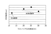
図4は、本実施形態の実施例と従来例のラストバリア層14c膜厚と相対発光強度を示すグラフである。ラストバリア層14cの成長後に成長を中断して昇温をした従来例をグラフ中に▲でプロットし、昇温成長工程で昇温中にラストバリア層14cの成長を継続した実施例をグラフ中に◆でプロットしている。
FIG. 4 is a graph showing the film thickness and relative light emission intensity of the
従来例のラストバリア層14cの膜厚は12nmであり、各実施例では定温成長工程で従来例と同様に12nm成長させた後に昇温成長工程でラストバリア層14cの成長を継続し、最終的に得られたラストバリア層14cの膜厚がそれぞれ20nm、25nm、30nmであった。図4に示したように、実施例では平均して従来例の1.37倍の発光強度となっており、発光効率が向上していることがわかる。
The film thickness of the
半導体発光素子1では、ラストバリア層14c上にMgがドープされた電子ブロック層15が形成されており、後工程での加熱等により電子ブロック層15中の不純物であるMgが発光層14側に拡散してくる。このMgが発光層14の内部まで拡散して井戸層14bに到達してしまうと、多重量子井戸構造が乱されて結晶品質が低下し、発光効率が低下してしまう。
In the semiconductor
しかし、本実施形態ではラストバリア層14cを他のバリア層14aよりも厚くしていることで、電子ブロック層15のMgが拡散してもラストバリア層14cの内部でMgの拡散を止めることができる。つまり、ラストバリア層14cの電子ブロック層15側にはMgが拡散されている拡散領域が形成され、井戸層14b側はMgが到達していない非拡散領域となっている。これにより、電子ブロック層15の不純物が井戸層14bまで到達して発光効率が低下することを防止することができる。
However, in the present embodiment, since the
本実施形態では、ラストバリア層14cを他のバリア層14aと同程度の厚さ定温成長工程で成長させた例を示したが、他のバリア層14aの膜厚以上を定温成長工程で成長させてさらに昇温成長工程でラストバリア層14cの成長を継続して厚膜化するとしてもよい。
In the present embodiment, the
本実施形態では、昇温成長工程で昇温中にもラストバリア層14cの成長を継続するため、ラストバリア層14cと電子ブロック層15の界面が劣化せず、結晶品質を維持して発光効率を向上させることができる。また、ラストバリア層14cの膜厚は他のバリア層14aよりも厚く、バリア層14aの1.5〜3倍程度の膜厚に形成される。これにより、電子ブロック層15にドープされたp型不純物であるMgが後工程で熱拡散しても、ラストバリア層14cの内部で拡散を止めることができ、発光層14の多重量子井戸構造への不純物拡散の影響を抑制して発光効率を向上することができる。
In the present embodiment, since the growth of the
(第2実施形態)
次に、本発明の第2実施形態について図5を用いて説明する。本実施形態では、昇温成長工程の後にもラストバリア層14cの成長を継続する点が第1実施形態と異なっており、重複する説明は省略する。図5は、本実施形態におけるラストバリア層14cからp型GaNコンタクト層16までの成長工程を示すタイミングチャートである。
(Second Embodiment)
Next, a second embodiment of the present invention will be described with reference to FIG. This embodiment is different from the first embodiment in that the growth of the
第1実施形態と同様に、GaNバッファ層11、GaN下地層12、n型GaN下地層13、バリア層14aと井戸層14bの5周期を成長させ、定温成長工程でラストバリア層14cの一部としてGaN層を12nmの膜厚で形成する。
As in the first embodiment, five periods of the
次に、昇温成長工程で基板温度を800℃から900℃まで昇温しながら、ラストバリア層14cの成長を継続させ。また、基板温度が900℃に達してもキャリアガスと原料ガスの供給を継続し、後工程である電子ブロック層15の成長と同じ温度の定温でラストバリア層14cの成長を継続し、さらにラストバリア層14cを厚膜化する。
Next, the growth of the
その後は、第1実施形態と同様に電子ブロック層15およびp型GaNコンタクト層16を成長させ、n型GaN下地層13までのエッチング、n側電極形成、p側電極形成、およびダイシングの各工程を経て半導体発光素子1を得る。
Thereafter, the
本実施形態でも、昇温成長工程で昇温中にもラストバリア層14cの成長を継続するため、ラストバリア層14cと電子ブロック層15の界面が劣化せず、結晶品質を維持して発光効率を向上させることができる。また、昇温成長工程の後にもラストバリア層14cの成長を継続することによりラストバリア層14cを厚く形成することで、バリア層14aの1.5〜3倍程度の膜厚にラストバリア層14cを形成する。これにより、電子ブロック層15にドープされたp型不純物であるMgが後工程で熱拡散しても、ラストバリア層14cの内部で拡散を止めることができ、発光層14の多重量子井戸構造への不純物拡散の影響を抑制して発光効率を向上することができる。
Also in this embodiment, since the growth of the
(第3実施形態)
第1実施形態および第2実施形態では、ラストバリア層14cをGaNとし電子ブロック層15をAlGaNとしたが、両者をAl組成が異なるAlGaNとして、電子ブロック層15のバンドギャップがラストバリア層14cよりも大きい構成としてもよい。また、他の材料系としてAl、In、B、Gaを含めた多元系材料であってもよい。
(Third embodiment)
In the first and second embodiments, the
さらに、本発明は窒化物系半導体材料に限定されず、他の半導体材料系であっても適用可能であり、例えばZnOなどの酸化物系半導体材料であっても適用可能である。酸化物系半導体材料の場合には、井戸層としてZnOを用い、バリア層および電子ブロック層としてMgZnOを用いることができる。 Furthermore, the present invention is not limited to the nitride-based semiconductor material, and can be applied to other semiconductor material systems, for example, an oxide-based semiconductor material such as ZnO. In the case of an oxide-based semiconductor material, ZnO can be used as the well layer, and MgZnO can be used as the barrier layer and the electron block layer.
いずれの材料系であっても、昇温成長工程で昇温中にもラストバリア層14cの成長を継続するため、ラストバリア層14cと電子ブロック層15の界面が劣化せず、結晶品質を維持して発光効率を向上させることができる。また、昇温成長工程の後にもラストバリア層14cの成長を継続することによりラストバリア層14cを厚く形成することで、バリア層14aの1.5〜3倍程度の膜厚にラストバリア層14cを形成する。これにより、電子ブロック層15にドープされたp型不純物であるMgが後工程で熱拡散しても、ラストバリア層14cの内部で拡散を止めることができ、発光層14の多重量子井戸構造への不純物拡散の影響を抑制して発光効率を向上させることができる。
Regardless of the material system, the growth of the
本発明は上述した各実施形態に限定されるものではなく、請求項に示した範囲で種々の変更が可能であり、異なる実施形態にそれぞれ開示された技術的手段を適宜組み合わせて得られる実施形態についても本発明の技術的範囲に含まれる。 The present invention is not limited to the above-described embodiments, and various modifications are possible within the scope shown in the claims, and embodiments obtained by appropriately combining technical means disclosed in different embodiments. Is also included in the technical scope of the present invention.
1…半導体発光素子
10…サファイア基板
11…GaNバッファ層
12…GaN下地層
13…n型GaN下地層
14…発光層
14a…バリア層
14b…井戸層
14c…ラストバリア層
15…電子ブロック層
16…p型GaNコンタクト層
DESCRIPTION OF
Claims (7)
前記障壁層のうち最上層であるラストバリア層は、他の前記障壁層よりも厚く、前記電子ブロック層からの不純物が拡散されている拡散領域と、前記電子ブロック層からの不純物が到達していない非拡散領域とを備えていることを特徴とする半導体発光素子。 A semiconductor light emitting device comprising a multi-quantum well active layer in which barrier layers and well layers are alternately stacked, and an electron block layer formed on the multi-quantum well active layer,
The last barrier layer, which is the uppermost layer among the barrier layers, is thicker than the other barrier layers, and has a diffusion region in which impurities from the electron blocking layer are diffused and impurities from the electron blocking layer reach. And a non-diffusing region.
前記ラストバリア層の膜厚は、前記他の障壁層の膜厚の1.5〜3倍であることを特徴とする半導体発光素子。 The semiconductor light emitting device according to claim 1,
The thickness of the last barrier layer is 1.5 to 3 times the thickness of the other barrier layer.
前記ラストバリア層の膜厚は、20nm以上30nm以下の範囲であることを特徴とする半導体発光素子。 The semiconductor light-emitting device according to claim 1 or 2,
A film thickness of the last barrier layer ranges from 20 nm to 30 nm.
前記障壁層のうち最上層であるラストバリア層を成長させる工程は、他の前記障壁層と同じ温度条件で結晶成長させる定温成長工程と、前記定温成長工程の後に成長温度を上昇させながら結晶成長を継続する昇温成長工程とを備えることを特徴とする半導体発光素子の製造方法。 A method of manufacturing a semiconductor light emitting device, comprising: growing a multiple quantum well active layer in which barrier layers and well layers are alternately stacked; and growing an electron block layer on the multiple quantum well active layer,
The step of growing the last barrier layer, the uppermost layer among the barrier layers, includes a constant temperature growth step of growing crystals under the same temperature conditions as the other barrier layers, and a crystal growth while increasing the growth temperature after the constant temperature growth step. And a temperature rising growth process for continuing the process.
前記ラストバリア層の膜厚は、前記他の障壁層の膜厚よりも厚いことを特徴とする半導体発光素子の製造方法。 It is a manufacturing method of the semiconductor light emitting element according to claim 4,
The method of manufacturing a semiconductor light emitting device, wherein the film thickness of the last barrier layer is larger than the film thickness of the other barrier layer.
前記定温成長工程で成長させる前記ラストバリア層の膜厚は、前記他の障壁層の膜厚以上であることを特徴とする半導体発光素子の製造方法。 It is a manufacturing method of the semiconductor light emitting element according to claim 4 or 5,
The method of manufacturing a semiconductor light emitting element, wherein the film thickness of the last barrier layer grown in the constant temperature growth step is equal to or greater than the film thickness of the other barrier layer.
前記電子ブロック層の成長時および成長後に、前記電子ブロック層から前記ラストバリア層に不純物の拡散が生じ、前記ラストバリア層に前記電子ブロック層からの不純物が拡散されている拡散領域と、前記電子ブロック層からの不純物が到達していない非拡散領域とを形成することを特徴とする半導体発光素子の製造方法。 A method of manufacturing a semiconductor light emitting device according to any one of claims 4 to 6,
During and after the growth of the electron blocking layer, diffusion of impurities from the electron blocking layer to the last barrier layer occurs, and a diffusion region in which impurities from the electron blocking layer are diffused into the last barrier layer, and the electrons A method of manufacturing a semiconductor light emitting element, comprising forming a non-diffusion region to which impurities from a block layer have not reached.
Priority Applications (1)
| Application Number | Priority Date | Filing Date | Title |
|---|---|---|---|
| JP2015248898A JP6884505B2 (en) | 2015-12-21 | 2015-12-21 | Semiconductor light emitting device and its manufacturing method |
Applications Claiming Priority (1)
| Application Number | Priority Date | Filing Date | Title |
|---|---|---|---|
| JP2015248898A JP6884505B2 (en) | 2015-12-21 | 2015-12-21 | Semiconductor light emitting device and its manufacturing method |
Publications (2)
| Publication Number | Publication Date |
|---|---|
| JP2017117845A true JP2017117845A (en) | 2017-06-29 |
| JP6884505B2 JP6884505B2 (en) | 2021-06-09 |
Family
ID=59232018
Family Applications (1)
| Application Number | Title | Priority Date | Filing Date |
|---|---|---|---|
| JP2015248898A Active JP6884505B2 (en) | 2015-12-21 | 2015-12-21 | Semiconductor light emitting device and its manufacturing method |
Country Status (1)
| Country | Link |
|---|---|
| JP (1) | JP6884505B2 (en) |
Cited By (1)
| Publication number | Priority date | Publication date | Assignee | Title |
|---|---|---|---|---|
| WO2022262315A1 (en) * | 2021-06-15 | 2022-12-22 | 厦门士兰明镓化合物半导体有限公司 | Semiconductor light-emitting element |
Citations (7)
| Publication number | Priority date | Publication date | Assignee | Title |
|---|---|---|---|---|
| WO2008153065A1 (en) * | 2007-06-15 | 2008-12-18 | Rohm Co., Ltd. | Semiconductor light emitting element and method for manufacturing the same |
| JP2010141242A (en) * | 2008-12-15 | 2010-06-24 | Opnext Japan Inc | Nitride semiconductor optical element and manufacturing method thereof |
| JP2012114328A (en) * | 2010-11-26 | 2012-06-14 | Toshiba Corp | Optical semiconductor element |
| JP2012119515A (en) * | 2010-12-01 | 2012-06-21 | Toshiba Corp | Semiconductor light-emitting element |
| KR20130008141A (en) * | 2011-07-12 | 2013-01-22 | 엘지이노텍 주식회사 | Light emitting device |
| JP2013038394A (en) * | 2011-07-14 | 2013-02-21 | Rohm Co Ltd | Semiconductor laser element |
| JP2015115433A (en) * | 2013-12-11 | 2015-06-22 | 学校法人 名城大学 | Group iii nitride semiconductor element |
-
2015
- 2015-12-21 JP JP2015248898A patent/JP6884505B2/en active Active
Patent Citations (7)
| Publication number | Priority date | Publication date | Assignee | Title |
|---|---|---|---|---|
| WO2008153065A1 (en) * | 2007-06-15 | 2008-12-18 | Rohm Co., Ltd. | Semiconductor light emitting element and method for manufacturing the same |
| JP2010141242A (en) * | 2008-12-15 | 2010-06-24 | Opnext Japan Inc | Nitride semiconductor optical element and manufacturing method thereof |
| JP2012114328A (en) * | 2010-11-26 | 2012-06-14 | Toshiba Corp | Optical semiconductor element |
| JP2012119515A (en) * | 2010-12-01 | 2012-06-21 | Toshiba Corp | Semiconductor light-emitting element |
| KR20130008141A (en) * | 2011-07-12 | 2013-01-22 | 엘지이노텍 주식회사 | Light emitting device |
| JP2013038394A (en) * | 2011-07-14 | 2013-02-21 | Rohm Co Ltd | Semiconductor laser element |
| JP2015115433A (en) * | 2013-12-11 | 2015-06-22 | 学校法人 名城大学 | Group iii nitride semiconductor element |
Cited By (1)
| Publication number | Priority date | Publication date | Assignee | Title |
|---|---|---|---|---|
| WO2022262315A1 (en) * | 2021-06-15 | 2022-12-22 | 厦门士兰明镓化合物半导体有限公司 | Semiconductor light-emitting element |
Also Published As
| Publication number | Publication date |
|---|---|
| JP6884505B2 (en) | 2021-06-09 |
Similar Documents
| Publication | Publication Date | Title |
|---|---|---|
| US10283671B2 (en) | Method of producing III nitride semiconductor light-emitting device | |
| JP5048236B2 (en) | Semiconductor light emitting device and method for manufacturing semiconductor light emitting device | |
| KR20180082424A (en) | Nitride semiconductor light emitting element | |
| JPWO2008153130A1 (en) | Nitride semiconductor light emitting device and method for manufacturing nitride semiconductor | |
| JP2006108585A (en) | Group iii nitride compound semiconductor light emitting element | |
| JP5279006B2 (en) | Nitride semiconductor light emitting device | |
| JPH10126006A (en) | Nitride semiconductor device | |
| JP2015149342A (en) | Semiconductor light-emitting element and method of manufacturing the same | |
| JP6001627B2 (en) | Group III nitride semiconductor light emitting device manufacturing method | |
| JP2006210692A (en) | Group iii nitride compound semiconductor light emitting device | |
| JP6725242B2 (en) | Semiconductor light emitting device and manufacturing method thereof | |
| JP3773713B2 (en) | Method for forming quantum box | |
| JP2008288532A (en) | Nitride semiconductor device | |
| JP5858246B2 (en) | Nitride semiconductor light emitting device and manufacturing method thereof | |
| JP2012204540A (en) | Semiconductor device and method of manufacturing the same | |
| TW201607076A (en) | Led element | |
| JP2010199236A (en) | Light emitting element producing method and light emitting element | |
| JP2007200933A (en) | Method of manufacturing nitride-based semiconductor element | |
| JP6884505B2 (en) | Semiconductor light emitting device and its manufacturing method | |
| JP2008118048A (en) | GaN-BASED SEMICONDUCTOR LIGHT EMITTING DEVICE | |
| JP2007214378A (en) | Nitride-based semiconductor element | |
| JP2006128653A (en) | Group iii-v compound semiconductor, its manufacturing method and its use | |
| JP2008227103A (en) | GaN-BASED SEMICONDUCTOR LIGHT EMITTING ELEMENT | |
| JP2007214251A (en) | Manufacturing method of nitride-based semiconductor element | |
| JP2005328093A (en) | Manufacturing method for compound semiconductor equipment |
Legal Events
| Date | Code | Title | Description |
|---|---|---|---|
| A621 | Written request for application examination |
Free format text: JAPANESE INTERMEDIATE CODE: A621 Effective date: 20181106 |
|
| A977 | Report on retrieval |
Free format text: JAPANESE INTERMEDIATE CODE: A971007 Effective date: 20190930 |
|
| A131 | Notification of reasons for refusal |
Free format text: JAPANESE INTERMEDIATE CODE: A131 Effective date: 20191015 |
|
| A521 | Request for written amendment filed |
Free format text: JAPANESE INTERMEDIATE CODE: A523 Effective date: 20191212 |
|
| A131 | Notification of reasons for refusal |
Free format text: JAPANESE INTERMEDIATE CODE: A131 Effective date: 20200324 |
|
| A521 | Request for written amendment filed |
Free format text: JAPANESE INTERMEDIATE CODE: A523 Effective date: 20200518 |
|
| A131 | Notification of reasons for refusal |
Free format text: JAPANESE INTERMEDIATE CODE: A131 Effective date: 20201013 |
|
| A521 | Request for written amendment filed |
Free format text: JAPANESE INTERMEDIATE CODE: A523 Effective date: 20201130 |
|
| TRDD | Decision of grant or rejection written | ||
| A01 | Written decision to grant a patent or to grant a registration (utility model) |
Free format text: JAPANESE INTERMEDIATE CODE: A01 Effective date: 20210420 |
|
| A61 | First payment of annual fees (during grant procedure) |
Free format text: JAPANESE INTERMEDIATE CODE: A61 Effective date: 20210512 |
|
| R150 | Certificate of patent or registration of utility model |
Ref document number: 6884505 Country of ref document: JP Free format text: JAPANESE INTERMEDIATE CODE: R150 |